JP6710627B2 - Semiconductor device and manufacturing method thereof - Google Patents
Semiconductor device and manufacturing method thereof Download PDFInfo
- Publication number
- JP6710627B2 JP6710627B2 JP2016246521A JP2016246521A JP6710627B2 JP 6710627 B2 JP6710627 B2 JP 6710627B2 JP 2016246521 A JP2016246521 A JP 2016246521A JP 2016246521 A JP2016246521 A JP 2016246521A JP 6710627 B2 JP6710627 B2 JP 6710627B2
- Authority
- JP
- Japan
- Prior art keywords
- region
- recess
- semiconductor device
- insulating film
- main surface
- Prior art date
- Legal status (The legal status is an assumption and is not a legal conclusion. Google has not performed a legal analysis and makes no representation as to the accuracy of the status listed.)
- Active
Links
- 239000004065 semiconductor Substances 0.000 title claims description 100
- 238000004519 manufacturing process Methods 0.000 title claims description 32
- 239000012535 impurity Substances 0.000 claims description 125
- 238000002955 isolation Methods 0.000 claims description 68
- 239000000758 substrate Substances 0.000 claims description 44
- 238000000926 separation method Methods 0.000 claims description 15
- 239000011248 coating agent Substances 0.000 claims 1
- 238000000576 coating method Methods 0.000 claims 1
- 230000000149 penetrating effect Effects 0.000 claims 1
- 239000010410 layer Substances 0.000 description 31
- 230000000052 comparative effect Effects 0.000 description 29
- 238000000034 method Methods 0.000 description 25
- 230000015556 catabolic process Effects 0.000 description 21
- 230000000694 effects Effects 0.000 description 19
- 101100260895 Mus musculus Tnnc2 gene Proteins 0.000 description 17
- 239000000969 carrier Substances 0.000 description 16
- 230000005684 electric field Effects 0.000 description 16
- 238000002347 injection Methods 0.000 description 16
- 239000007924 injection Substances 0.000 description 16
- 238000005530 etching Methods 0.000 description 14
- 229920002120 photoresistant polymer Polymers 0.000 description 9
- 238000009826 distribution Methods 0.000 description 8
- 239000011229 interlayer Substances 0.000 description 8
- 238000010586 diagram Methods 0.000 description 6
- 238000005468 ion implantation Methods 0.000 description 6
- 229910021420 polycrystalline silicon Inorganic materials 0.000 description 6
- VYPSYNLAJGMNEJ-UHFFFAOYSA-N Silicium dioxide Chemical compound O=[Si]=O VYPSYNLAJGMNEJ-UHFFFAOYSA-N 0.000 description 5
- 230000015572 biosynthetic process Effects 0.000 description 5
- 238000012986 modification Methods 0.000 description 5
- 230000004048 modification Effects 0.000 description 5
- 229920005591 polysilicon Polymers 0.000 description 5
- 229910052814 silicon oxide Inorganic materials 0.000 description 5
- 238000002513 implantation Methods 0.000 description 4
- 229910044991 metal oxide Inorganic materials 0.000 description 3
- 150000004706 metal oxides Chemical class 0.000 description 3
- 238000004380 ashing Methods 0.000 description 2
- 230000000295 complement effect Effects 0.000 description 2
- 230000007423 decrease Effects 0.000 description 2
- 239000000463 material Substances 0.000 description 2
- 238000004088 simulation Methods 0.000 description 2
- 229910052581 Si3N4 Inorganic materials 0.000 description 1
- XUIMIQQOPSSXEZ-UHFFFAOYSA-N Silicon Chemical compound [Si] XUIMIQQOPSSXEZ-UHFFFAOYSA-N 0.000 description 1
- 239000012141 concentrate Substances 0.000 description 1
- 239000012212 insulator Substances 0.000 description 1
- 150000002500 ions Chemical class 0.000 description 1
- 238000005259 measurement Methods 0.000 description 1
- 239000002184 metal Substances 0.000 description 1
- 230000003647 oxidation Effects 0.000 description 1
- 238000007254 oxidation reaction Methods 0.000 description 1
- 238000000206 photolithography Methods 0.000 description 1
- 238000005498 polishing Methods 0.000 description 1
- 230000002250 progressing effect Effects 0.000 description 1
- 239000011347 resin Substances 0.000 description 1
- 229920005989 resin Polymers 0.000 description 1
- 238000007789 sealing Methods 0.000 description 1
- 229910052710 silicon Inorganic materials 0.000 description 1
- 239000010703 silicon Substances 0.000 description 1
- HQVNEWCFYHHQES-UHFFFAOYSA-N silicon nitride Chemical compound N12[Si]34N5[Si]62N3[Si]51N64 HQVNEWCFYHHQES-UHFFFAOYSA-N 0.000 description 1
- 239000000126 substance Substances 0.000 description 1
Images


Classifications
-
- H—ELECTRICITY
- H01—ELECTRIC ELEMENTS
- H01L—SEMICONDUCTOR DEVICES NOT COVERED BY CLASS H10
- H01L29/00—Semiconductor devices adapted for rectifying, amplifying, oscillating or switching, or capacitors or resistors with at least one potential-jump barrier or surface barrier, e.g. PN junction depletion layer or carrier concentration layer; Details of semiconductor bodies or of electrodes thereof ; Multistep manufacturing processes therefor
- H01L29/66—Types of semiconductor device ; Multistep manufacturing processes therefor
- H01L29/68—Types of semiconductor device ; Multistep manufacturing processes therefor controllable by only the electric current supplied, or only the electric potential applied, to an electrode which does not carry the current to be rectified, amplified or switched
- H01L29/76—Unipolar devices, e.g. field effect transistors
- H01L29/772—Field effect transistors
- H01L29/78—Field effect transistors with field effect produced by an insulated gate
- H01L29/7801—DMOS transistors, i.e. MISFETs with a channel accommodating body or base region adjoining a drain drift region
- H01L29/7816—Lateral DMOS transistors, i.e. LDMOS transistors
-
- H—ELECTRICITY
- H01—ELECTRIC ELEMENTS
- H01L—SEMICONDUCTOR DEVICES NOT COVERED BY CLASS H10
- H01L21/00—Processes or apparatus adapted for the manufacture or treatment of semiconductor or solid state devices or of parts thereof
- H01L21/70—Manufacture or treatment of devices consisting of a plurality of solid state components formed in or on a common substrate or of parts thereof; Manufacture of integrated circuit devices or of parts thereof
- H01L21/71—Manufacture of specific parts of devices defined in group H01L21/70
- H01L21/76—Making of isolation regions between components
- H01L21/762—Dielectric regions, e.g. EPIC dielectric isolation, LOCOS; Trench refilling techniques, SOI technology, use of channel stoppers
- H01L21/76224—Dielectric regions, e.g. EPIC dielectric isolation, LOCOS; Trench refilling techniques, SOI technology, use of channel stoppers using trench refilling with dielectric materials
-
- H—ELECTRICITY
- H01—ELECTRIC ELEMENTS
- H01L—SEMICONDUCTOR DEVICES NOT COVERED BY CLASS H10
- H01L21/00—Processes or apparatus adapted for the manufacture or treatment of semiconductor or solid state devices or of parts thereof
- H01L21/70—Manufacture or treatment of devices consisting of a plurality of solid state components formed in or on a common substrate or of parts thereof; Manufacture of integrated circuit devices or of parts thereof
- H01L21/71—Manufacture of specific parts of devices defined in group H01L21/70
- H01L21/76—Making of isolation regions between components
- H01L21/762—Dielectric regions, e.g. EPIC dielectric isolation, LOCOS; Trench refilling techniques, SOI technology, use of channel stoppers
-
- H—ELECTRICITY
- H01—ELECTRIC ELEMENTS
- H01L—SEMICONDUCTOR DEVICES NOT COVERED BY CLASS H10
- H01L29/00—Semiconductor devices adapted for rectifying, amplifying, oscillating or switching, or capacitors or resistors with at least one potential-jump barrier or surface barrier, e.g. PN junction depletion layer or carrier concentration layer; Details of semiconductor bodies or of electrodes thereof ; Multistep manufacturing processes therefor
- H01L29/02—Semiconductor bodies ; Multistep manufacturing processes therefor
- H01L29/06—Semiconductor bodies ; Multistep manufacturing processes therefor characterised by their shape; characterised by the shapes, relative sizes, or dispositions of the semiconductor regions ; characterised by the concentration or distribution of impurities within semiconductor regions
- H01L29/0603—Semiconductor bodies ; Multistep manufacturing processes therefor characterised by their shape; characterised by the shapes, relative sizes, or dispositions of the semiconductor regions ; characterised by the concentration or distribution of impurities within semiconductor regions characterised by particular constructional design considerations, e.g. for preventing surface leakage, for controlling electric field concentration or for internal isolations regions
- H01L29/0607—Semiconductor bodies ; Multistep manufacturing processes therefor characterised by their shape; characterised by the shapes, relative sizes, or dispositions of the semiconductor regions ; characterised by the concentration or distribution of impurities within semiconductor regions characterised by particular constructional design considerations, e.g. for preventing surface leakage, for controlling electric field concentration or for internal isolations regions for preventing surface leakage or controlling electric field concentration
- H01L29/0611—Semiconductor bodies ; Multistep manufacturing processes therefor characterised by their shape; characterised by the shapes, relative sizes, or dispositions of the semiconductor regions ; characterised by the concentration or distribution of impurities within semiconductor regions characterised by particular constructional design considerations, e.g. for preventing surface leakage, for controlling electric field concentration or for internal isolations regions for preventing surface leakage or controlling electric field concentration for increasing or controlling the breakdown voltage of reverse biased devices
- H01L29/0615—Semiconductor bodies ; Multistep manufacturing processes therefor characterised by their shape; characterised by the shapes, relative sizes, or dispositions of the semiconductor regions ; characterised by the concentration or distribution of impurities within semiconductor regions characterised by particular constructional design considerations, e.g. for preventing surface leakage, for controlling electric field concentration or for internal isolations regions for preventing surface leakage or controlling electric field concentration for increasing or controlling the breakdown voltage of reverse biased devices by the doping profile or the shape or the arrangement of the PN junction, or with supplementary regions, e.g. junction termination extension [JTE]
- H01L29/063—Reduced surface field [RESURF] pn-junction structures
-
- H—ELECTRICITY
- H01—ELECTRIC ELEMENTS
- H01L—SEMICONDUCTOR DEVICES NOT COVERED BY CLASS H10
- H01L29/00—Semiconductor devices adapted for rectifying, amplifying, oscillating or switching, or capacitors or resistors with at least one potential-jump barrier or surface barrier, e.g. PN junction depletion layer or carrier concentration layer; Details of semiconductor bodies or of electrodes thereof ; Multistep manufacturing processes therefor
- H01L29/02—Semiconductor bodies ; Multistep manufacturing processes therefor
- H01L29/06—Semiconductor bodies ; Multistep manufacturing processes therefor characterised by their shape; characterised by the shapes, relative sizes, or dispositions of the semiconductor regions ; characterised by the concentration or distribution of impurities within semiconductor regions
- H01L29/0603—Semiconductor bodies ; Multistep manufacturing processes therefor characterised by their shape; characterised by the shapes, relative sizes, or dispositions of the semiconductor regions ; characterised by the concentration or distribution of impurities within semiconductor regions characterised by particular constructional design considerations, e.g. for preventing surface leakage, for controlling electric field concentration or for internal isolations regions
- H01L29/0642—Isolation within the component, i.e. internal isolation
- H01L29/0649—Dielectric regions, e.g. SiO2 regions, air gaps
- H01L29/0653—Dielectric regions, e.g. SiO2 regions, air gaps adjoining the input or output region of a field-effect device, e.g. the source or drain region
-
- H—ELECTRICITY
- H01—ELECTRIC ELEMENTS
- H01L—SEMICONDUCTOR DEVICES NOT COVERED BY CLASS H10
- H01L29/00—Semiconductor devices adapted for rectifying, amplifying, oscillating or switching, or capacitors or resistors with at least one potential-jump barrier or surface barrier, e.g. PN junction depletion layer or carrier concentration layer; Details of semiconductor bodies or of electrodes thereof ; Multistep manufacturing processes therefor
- H01L29/02—Semiconductor bodies ; Multistep manufacturing processes therefor
- H01L29/06—Semiconductor bodies ; Multistep manufacturing processes therefor characterised by their shape; characterised by the shapes, relative sizes, or dispositions of the semiconductor regions ; characterised by the concentration or distribution of impurities within semiconductor regions
- H01L29/08—Semiconductor bodies ; Multistep manufacturing processes therefor characterised by their shape; characterised by the shapes, relative sizes, or dispositions of the semiconductor regions ; characterised by the concentration or distribution of impurities within semiconductor regions with semiconductor regions connected to an electrode carrying current to be rectified, amplified or switched and such electrode being part of a semiconductor device which comprises three or more electrodes
- H01L29/0843—Source or drain regions of field-effect devices
- H01L29/0847—Source or drain regions of field-effect devices of field-effect transistors with insulated gate
- H01L29/0852—Source or drain regions of field-effect devices of field-effect transistors with insulated gate of DMOS transistors
- H01L29/0856—Source regions
- H01L29/0865—Disposition
-
- H—ELECTRICITY
- H01—ELECTRIC ELEMENTS
- H01L—SEMICONDUCTOR DEVICES NOT COVERED BY CLASS H10
- H01L29/00—Semiconductor devices adapted for rectifying, amplifying, oscillating or switching, or capacitors or resistors with at least one potential-jump barrier or surface barrier, e.g. PN junction depletion layer or carrier concentration layer; Details of semiconductor bodies or of electrodes thereof ; Multistep manufacturing processes therefor
- H01L29/02—Semiconductor bodies ; Multistep manufacturing processes therefor
- H01L29/06—Semiconductor bodies ; Multistep manufacturing processes therefor characterised by their shape; characterised by the shapes, relative sizes, or dispositions of the semiconductor regions ; characterised by the concentration or distribution of impurities within semiconductor regions
- H01L29/08—Semiconductor bodies ; Multistep manufacturing processes therefor characterised by their shape; characterised by the shapes, relative sizes, or dispositions of the semiconductor regions ; characterised by the concentration or distribution of impurities within semiconductor regions with semiconductor regions connected to an electrode carrying current to be rectified, amplified or switched and such electrode being part of a semiconductor device which comprises three or more electrodes
- H01L29/0843—Source or drain regions of field-effect devices
- H01L29/0847—Source or drain regions of field-effect devices of field-effect transistors with insulated gate
- H01L29/0852—Source or drain regions of field-effect devices of field-effect transistors with insulated gate of DMOS transistors
- H01L29/0873—Drain regions
- H01L29/0882—Disposition
-
- H—ELECTRICITY
- H01—ELECTRIC ELEMENTS
- H01L—SEMICONDUCTOR DEVICES NOT COVERED BY CLASS H10
- H01L29/00—Semiconductor devices adapted for rectifying, amplifying, oscillating or switching, or capacitors or resistors with at least one potential-jump barrier or surface barrier, e.g. PN junction depletion layer or carrier concentration layer; Details of semiconductor bodies or of electrodes thereof ; Multistep manufacturing processes therefor
- H01L29/02—Semiconductor bodies ; Multistep manufacturing processes therefor
- H01L29/06—Semiconductor bodies ; Multistep manufacturing processes therefor characterised by their shape; characterised by the shapes, relative sizes, or dispositions of the semiconductor regions ; characterised by the concentration or distribution of impurities within semiconductor regions
- H01L29/10—Semiconductor bodies ; Multistep manufacturing processes therefor characterised by their shape; characterised by the shapes, relative sizes, or dispositions of the semiconductor regions ; characterised by the concentration or distribution of impurities within semiconductor regions with semiconductor regions connected to an electrode not carrying current to be rectified, amplified or switched and such electrode being part of a semiconductor device which comprises three or more electrodes
- H01L29/1095—Body region, i.e. base region, of DMOS transistors or IGBTs
-
- H—ELECTRICITY
- H01—ELECTRIC ELEMENTS
- H01L—SEMICONDUCTOR DEVICES NOT COVERED BY CLASS H10
- H01L29/00—Semiconductor devices adapted for rectifying, amplifying, oscillating or switching, or capacitors or resistors with at least one potential-jump barrier or surface barrier, e.g. PN junction depletion layer or carrier concentration layer; Details of semiconductor bodies or of electrodes thereof ; Multistep manufacturing processes therefor
- H01L29/40—Electrodes ; Multistep manufacturing processes therefor
- H01L29/41—Electrodes ; Multistep manufacturing processes therefor characterised by their shape, relative sizes or dispositions
- H01L29/423—Electrodes ; Multistep manufacturing processes therefor characterised by their shape, relative sizes or dispositions not carrying the current to be rectified, amplified or switched
- H01L29/42312—Gate electrodes for field effect devices
- H01L29/42316—Gate electrodes for field effect devices for field-effect transistors
- H01L29/4232—Gate electrodes for field effect devices for field-effect transistors with insulated gate
- H01L29/42356—Disposition, e.g. buried gate electrode
- H01L29/4236—Disposition, e.g. buried gate electrode within a trench, e.g. trench gate electrode, groove gate electrode
-
- H—ELECTRICITY
- H01—ELECTRIC ELEMENTS
- H01L—SEMICONDUCTOR DEVICES NOT COVERED BY CLASS H10
- H01L29/00—Semiconductor devices adapted for rectifying, amplifying, oscillating or switching, or capacitors or resistors with at least one potential-jump barrier or surface barrier, e.g. PN junction depletion layer or carrier concentration layer; Details of semiconductor bodies or of electrodes thereof ; Multistep manufacturing processes therefor
- H01L29/40—Electrodes ; Multistep manufacturing processes therefor
- H01L29/41—Electrodes ; Multistep manufacturing processes therefor characterised by their shape, relative sizes or dispositions
- H01L29/423—Electrodes ; Multistep manufacturing processes therefor characterised by their shape, relative sizes or dispositions not carrying the current to be rectified, amplified or switched
- H01L29/42312—Gate electrodes for field effect devices
- H01L29/42316—Gate electrodes for field effect devices for field-effect transistors
- H01L29/4232—Gate electrodes for field effect devices for field-effect transistors with insulated gate
- H01L29/42364—Gate electrodes for field effect devices for field-effect transistors with insulated gate characterised by the insulating layer, e.g. thickness or uniformity
- H01L29/42368—Gate electrodes for field effect devices for field-effect transistors with insulated gate characterised by the insulating layer, e.g. thickness or uniformity the thickness being non-uniform
-
- H—ELECTRICITY
- H01—ELECTRIC ELEMENTS
- H01L—SEMICONDUCTOR DEVICES NOT COVERED BY CLASS H10
- H01L29/00—Semiconductor devices adapted for rectifying, amplifying, oscillating or switching, or capacitors or resistors with at least one potential-jump barrier or surface barrier, e.g. PN junction depletion layer or carrier concentration layer; Details of semiconductor bodies or of electrodes thereof ; Multistep manufacturing processes therefor
- H01L29/66—Types of semiconductor device ; Multistep manufacturing processes therefor
- H01L29/66007—Multistep manufacturing processes
- H01L29/66075—Multistep manufacturing processes of devices having semiconductor bodies comprising group 14 or group 13/15 materials
- H01L29/66227—Multistep manufacturing processes of devices having semiconductor bodies comprising group 14 or group 13/15 materials the devices being controllable only by the electric current supplied or the electric potential applied, to an electrode which does not carry the current to be rectified, amplified or switched, e.g. three-terminal devices
- H01L29/66409—Unipolar field-effect transistors
- H01L29/66477—Unipolar field-effect transistors with an insulated gate, i.e. MISFET
- H01L29/66568—Lateral single gate silicon transistors
- H01L29/66659—Lateral single gate silicon transistors with asymmetry in the channel direction, e.g. lateral high-voltage MISFETs with drain offset region, extended drain MISFETs
-
- H—ELECTRICITY
- H01—ELECTRIC ELEMENTS
- H01L—SEMICONDUCTOR DEVICES NOT COVERED BY CLASS H10
- H01L29/00—Semiconductor devices adapted for rectifying, amplifying, oscillating or switching, or capacitors or resistors with at least one potential-jump barrier or surface barrier, e.g. PN junction depletion layer or carrier concentration layer; Details of semiconductor bodies or of electrodes thereof ; Multistep manufacturing processes therefor
- H01L29/66—Types of semiconductor device ; Multistep manufacturing processes therefor
- H01L29/66007—Multistep manufacturing processes
- H01L29/66075—Multistep manufacturing processes of devices having semiconductor bodies comprising group 14 or group 13/15 materials
- H01L29/66227—Multistep manufacturing processes of devices having semiconductor bodies comprising group 14 or group 13/15 materials the devices being controllable only by the electric current supplied or the electric potential applied, to an electrode which does not carry the current to be rectified, amplified or switched, e.g. three-terminal devices
- H01L29/66409—Unipolar field-effect transistors
- H01L29/66477—Unipolar field-effect transistors with an insulated gate, i.e. MISFET
- H01L29/66674—DMOS transistors, i.e. MISFETs with a channel accommodating body or base region adjoining a drain drift region
- H01L29/66681—Lateral DMOS transistors, i.e. LDMOS transistors
-
- H—ELECTRICITY
- H01—ELECTRIC ELEMENTS
- H01L—SEMICONDUCTOR DEVICES NOT COVERED BY CLASS H10
- H01L29/00—Semiconductor devices adapted for rectifying, amplifying, oscillating or switching, or capacitors or resistors with at least one potential-jump barrier or surface barrier, e.g. PN junction depletion layer or carrier concentration layer; Details of semiconductor bodies or of electrodes thereof ; Multistep manufacturing processes therefor
- H01L29/66—Types of semiconductor device ; Multistep manufacturing processes therefor
- H01L29/68—Types of semiconductor device ; Multistep manufacturing processes therefor controllable by only the electric current supplied, or only the electric potential applied, to an electrode which does not carry the current to be rectified, amplified or switched
- H01L29/76—Unipolar devices, e.g. field effect transistors
- H01L29/772—Field effect transistors
- H01L29/78—Field effect transistors with field effect produced by an insulated gate
- H01L29/7833—Field effect transistors with field effect produced by an insulated gate with lightly doped drain or source extension, e.g. LDD MOSFET's; DDD MOSFET's
- H01L29/7835—Field effect transistors with field effect produced by an insulated gate with lightly doped drain or source extension, e.g. LDD MOSFET's; DDD MOSFET's with asymmetrical source and drain regions, e.g. lateral high-voltage MISFETs with drain offset region, extended drain MISFETs
-
- H—ELECTRICITY
- H01—ELECTRIC ELEMENTS
- H01L—SEMICONDUCTOR DEVICES NOT COVERED BY CLASS H10
- H01L21/00—Processes or apparatus adapted for the manufacture or treatment of semiconductor or solid state devices or of parts thereof
- H01L21/02—Manufacture or treatment of semiconductor devices or of parts thereof
- H01L21/04—Manufacture or treatment of semiconductor devices or of parts thereof the devices having at least one potential-jump barrier or surface barrier, e.g. PN junction, depletion layer or carrier concentration layer
- H01L21/18—Manufacture or treatment of semiconductor devices or of parts thereof the devices having at least one potential-jump barrier or surface barrier, e.g. PN junction, depletion layer or carrier concentration layer the devices having semiconductor bodies comprising elements of Group IV of the Periodic System or AIIIBV compounds with or without impurities, e.g. doping materials
- H01L21/30—Treatment of semiconductor bodies using processes or apparatus not provided for in groups H01L21/20 - H01L21/26
- H01L21/31—Treatment of semiconductor bodies using processes or apparatus not provided for in groups H01L21/20 - H01L21/26 to form insulating layers thereon, e.g. for masking or by using photolithographic techniques; After treatment of these layers; Selection of materials for these layers
- H01L21/3105—After-treatment
- H01L21/31051—Planarisation of the insulating layers
- H01L21/31053—Planarisation of the insulating layers involving a dielectric removal step
-
- H—ELECTRICITY
- H01—ELECTRIC ELEMENTS
- H01L—SEMICONDUCTOR DEVICES NOT COVERED BY CLASS H10
- H01L21/00—Processes or apparatus adapted for the manufacture or treatment of semiconductor or solid state devices or of parts thereof
- H01L21/70—Manufacture or treatment of devices consisting of a plurality of solid state components formed in or on a common substrate or of parts thereof; Manufacture of integrated circuit devices or of parts thereof
- H01L21/77—Manufacture or treatment of devices consisting of a plurality of solid state components or integrated circuits formed in, or on, a common substrate
- H01L21/78—Manufacture or treatment of devices consisting of a plurality of solid state components or integrated circuits formed in, or on, a common substrate with subsequent division of the substrate into plural individual devices
- H01L21/82—Manufacture or treatment of devices consisting of a plurality of solid state components or integrated circuits formed in, or on, a common substrate with subsequent division of the substrate into plural individual devices to produce devices, e.g. integrated circuits, each consisting of a plurality of components
- H01L21/822—Manufacture or treatment of devices consisting of a plurality of solid state components or integrated circuits formed in, or on, a common substrate with subsequent division of the substrate into plural individual devices to produce devices, e.g. integrated circuits, each consisting of a plurality of components the substrate being a semiconductor, using silicon technology
- H01L21/8232—Field-effect technology
- H01L21/8234—MIS technology, i.e. integration processes of field effect transistors of the conductor-insulator-semiconductor type
- H01L21/8238—Complementary field-effect transistors, e.g. CMOS
- H01L21/823814—Complementary field-effect transistors, e.g. CMOS with a particular manufacturing method of the source or drain structures, e.g. specific source or drain implants or silicided source or drain structures or raised source or drain structures
-
- H—ELECTRICITY
- H01—ELECTRIC ELEMENTS
- H01L—SEMICONDUCTOR DEVICES NOT COVERED BY CLASS H10
- H01L27/00—Devices consisting of a plurality of semiconductor or other solid-state components formed in or on a common substrate
- H01L27/02—Devices consisting of a plurality of semiconductor or other solid-state components formed in or on a common substrate including semiconductor components specially adapted for rectifying, oscillating, amplifying or switching and having at least one potential-jump barrier or surface barrier; including integrated passive circuit elements with at least one potential-jump barrier or surface barrier
- H01L27/04—Devices consisting of a plurality of semiconductor or other solid-state components formed in or on a common substrate including semiconductor components specially adapted for rectifying, oscillating, amplifying or switching and having at least one potential-jump barrier or surface barrier; including integrated passive circuit elements with at least one potential-jump barrier or surface barrier the substrate being a semiconductor body
- H01L27/06—Devices consisting of a plurality of semiconductor or other solid-state components formed in or on a common substrate including semiconductor components specially adapted for rectifying, oscillating, amplifying or switching and having at least one potential-jump barrier or surface barrier; including integrated passive circuit elements with at least one potential-jump barrier or surface barrier the substrate being a semiconductor body including a plurality of individual components in a non-repetitive configuration
- H01L27/0611—Devices consisting of a plurality of semiconductor or other solid-state components formed in or on a common substrate including semiconductor components specially adapted for rectifying, oscillating, amplifying or switching and having at least one potential-jump barrier or surface barrier; including integrated passive circuit elements with at least one potential-jump barrier or surface barrier the substrate being a semiconductor body including a plurality of individual components in a non-repetitive configuration integrated circuits having a two-dimensional layout of components without a common active region
- H01L27/0617—Devices consisting of a plurality of semiconductor or other solid-state components formed in or on a common substrate including semiconductor components specially adapted for rectifying, oscillating, amplifying or switching and having at least one potential-jump barrier or surface barrier; including integrated passive circuit elements with at least one potential-jump barrier or surface barrier the substrate being a semiconductor body including a plurality of individual components in a non-repetitive configuration integrated circuits having a two-dimensional layout of components without a common active region comprising components of the field-effect type
- H01L27/0623—Devices consisting of a plurality of semiconductor or other solid-state components formed in or on a common substrate including semiconductor components specially adapted for rectifying, oscillating, amplifying or switching and having at least one potential-jump barrier or surface barrier; including integrated passive circuit elements with at least one potential-jump barrier or surface barrier the substrate being a semiconductor body including a plurality of individual components in a non-repetitive configuration integrated circuits having a two-dimensional layout of components without a common active region comprising components of the field-effect type in combination with bipolar transistors
-
- H—ELECTRICITY
- H01—ELECTRIC ELEMENTS
- H01L—SEMICONDUCTOR DEVICES NOT COVERED BY CLASS H10
- H01L27/00—Devices consisting of a plurality of semiconductor or other solid-state components formed in or on a common substrate
- H01L27/02—Devices consisting of a plurality of semiconductor or other solid-state components formed in or on a common substrate including semiconductor components specially adapted for rectifying, oscillating, amplifying or switching and having at least one potential-jump barrier or surface barrier; including integrated passive circuit elements with at least one potential-jump barrier or surface barrier
- H01L27/04—Devices consisting of a plurality of semiconductor or other solid-state components formed in or on a common substrate including semiconductor components specially adapted for rectifying, oscillating, amplifying or switching and having at least one potential-jump barrier or surface barrier; including integrated passive circuit elements with at least one potential-jump barrier or surface barrier the substrate being a semiconductor body
- H01L27/08—Devices consisting of a plurality of semiconductor or other solid-state components formed in or on a common substrate including semiconductor components specially adapted for rectifying, oscillating, amplifying or switching and having at least one potential-jump barrier or surface barrier; including integrated passive circuit elements with at least one potential-jump barrier or surface barrier the substrate being a semiconductor body including only semiconductor components of a single kind
- H01L27/085—Devices consisting of a plurality of semiconductor or other solid-state components formed in or on a common substrate including semiconductor components specially adapted for rectifying, oscillating, amplifying or switching and having at least one potential-jump barrier or surface barrier; including integrated passive circuit elements with at least one potential-jump barrier or surface barrier the substrate being a semiconductor body including only semiconductor components of a single kind including field-effect components only
- H01L27/088—Devices consisting of a plurality of semiconductor or other solid-state components formed in or on a common substrate including semiconductor components specially adapted for rectifying, oscillating, amplifying or switching and having at least one potential-jump barrier or surface barrier; including integrated passive circuit elements with at least one potential-jump barrier or surface barrier the substrate being a semiconductor body including only semiconductor components of a single kind including field-effect components only the components being field-effect transistors with insulated gate
- H01L27/092—Devices consisting of a plurality of semiconductor or other solid-state components formed in or on a common substrate including semiconductor components specially adapted for rectifying, oscillating, amplifying or switching and having at least one potential-jump barrier or surface barrier; including integrated passive circuit elements with at least one potential-jump barrier or surface barrier the substrate being a semiconductor body including only semiconductor components of a single kind including field-effect components only the components being field-effect transistors with insulated gate complementary MIS field-effect transistors
-
- H—ELECTRICITY
- H01—ELECTRIC ELEMENTS
- H01L—SEMICONDUCTOR DEVICES NOT COVERED BY CLASS H10
- H01L29/00—Semiconductor devices adapted for rectifying, amplifying, oscillating or switching, or capacitors or resistors with at least one potential-jump barrier or surface barrier, e.g. PN junction depletion layer or carrier concentration layer; Details of semiconductor bodies or of electrodes thereof ; Multistep manufacturing processes therefor
- H01L29/02—Semiconductor bodies ; Multistep manufacturing processes therefor
- H01L29/06—Semiconductor bodies ; Multistep manufacturing processes therefor characterised by their shape; characterised by the shapes, relative sizes, or dispositions of the semiconductor regions ; characterised by the concentration or distribution of impurities within semiconductor regions
- H01L29/10—Semiconductor bodies ; Multistep manufacturing processes therefor characterised by their shape; characterised by the shapes, relative sizes, or dispositions of the semiconductor regions ; characterised by the concentration or distribution of impurities within semiconductor regions with semiconductor regions connected to an electrode not carrying current to be rectified, amplified or switched and such electrode being part of a semiconductor device which comprises three or more electrodes
- H01L29/107—Substrate region of field-effect devices
- H01L29/1075—Substrate region of field-effect devices of field-effect transistors
- H01L29/1079—Substrate region of field-effect devices of field-effect transistors with insulated gate
- H01L29/1083—Substrate region of field-effect devices of field-effect transistors with insulated gate with an inactive supplementary region, e.g. for preventing punch-through, improving capacity effect or leakage current
Description
本発明は、半導体装置およびその製造方法に関するものである。 The present invention relates to a semiconductor device and its manufacturing method.
高耐圧化のために、高耐圧LDMOS(Laterally Diffused Metal Oxide Semiconductor)トランジスタのゲートとドレインとの間にSTI(Shallow Trench Isolation)構造を用いることが知られている。このような構造は、たとえば特開2015−162581号公報、特開2009−278100号公報などに開示されている。 It is known to use a STI (Shallow Trench Isolation) structure between a gate and a drain of a high breakdown voltage LDMOS (Laterally Diffused Metal Oxide Semiconductor) transistor for high breakdown voltage. Such a structure is disclosed in, for example, JP-A-2015-162581 and JP-A-2009-278100.
上記2つの公報には、分離溝内を埋め込む分離絶縁膜の上面に溝を形成し、その溝内にゲート電極の一部が埋め込まれた構成が開示されている。 The above two publications disclose a structure in which a groove is formed on the upper surface of an isolation insulating film filling the isolation groove, and a part of the gate electrode is embedded in the groove.
上記2つの公報に記載の構成では、ホットキャリア注入(HCI:Hot Carrier Injection)と呼ばれる現象を改善することが可能である。ここでホットキャリア注入とは、LDMOSトランジスタのドレイン電界によって加速され高いエネルギーを持ったキャリア(ホットキャリア)がゲート絶縁膜に注入されてトランジスタの特性(Ids、Vth)が変動する現象である。 With the configurations described in the above two publications, it is possible to improve a phenomenon called hot carrier injection (HCI). Here, hot carrier injection is a phenomenon in which carriers having high energy (hot carriers) accelerated by the drain electric field of the LDMOS transistor are injected into the gate insulating film and the characteristics (Ids, Vth) of the transistor change.
しかしながら、上記2つの公報に記載の技術では、ゲート絶縁膜へのホットキャリアの注入を抑制する効果が十分でない場合がある。 However, in the techniques described in the above two publications, the effect of suppressing the injection of hot carriers into the gate insulating film may not be sufficient.
その他の課題と新規な特徴は、本明細書の記述および添付図面から明らかになるであろう。 Other problems and novel features will be apparent from the description of the present specification and the accompanying drawings.
一実施の形態の半導体装置によれば、第1導電型のソース領域とドレイン領域との間の分離溝内を埋め込む分離絶縁膜の上面に凹部が形成されている。第1導電型のドリフト領域は、分離溝の下側に位置し、かつドレイン領域に接続されている。ゲート電極は、凹部内を埋め込んでいる。ドリフト領域の下側であって凹部の真下には、第2導電型の第1不純物領域が位置している。 According to the semiconductor device of the embodiment, the recess is formed in the upper surface of the isolation insulating film filling the isolation trench between the first conductivity type source region and the drain region. The drift region of the first conductivity type is located below the isolation trench and connected to the drain region. The gate electrode fills the inside of the recess. The first impurity region of the second conductivity type is located below the drift region and directly below the recess.
一実施の形態の半導体装置の製造方法によれば、分離溝内を埋め込み、かつ上面に凹部を有する分離絶縁膜が形成される。ドリフト領域の下側であって凹部の真下に位置する第2導電型の第1不純物領域が形成される。ソース領域とドリフト領域とに挟まれる主表面の上にゲート絶縁膜を挟んで対向し、かつ凹部内を埋め込むゲート電極が形成される。 According to the method of manufacturing the semiconductor device of the one embodiment, the isolation insulating film which fills the isolation trench and has the recessed portion on the upper surface is formed. A first impurity region of the second conductivity type located below the drift region and directly below the recess is formed. A gate electrode is formed on the main surface sandwiched between the source region and the drift region so as to face the gate insulating film and to fill the recess.
前記一実施の形態によれば、ゲート絶縁膜へのホットキャリアの注入をさらに抑制することが可能な半導体装置およびその製造方法を実現することができる。 According to the one embodiment, it is possible to realize a semiconductor device capable of further suppressing injection of hot carriers into the gate insulating film and a manufacturing method thereof.
以下、実施の形態について図に基づいて説明する。
(実施の形態1)
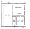
図1に示されるように、本実施の形態の半導体装置CHは、たとえばチップ状態であり、半導体基板を有している。半導体基板の表面には、ドライバ回路DRI、プリドライバ回路PDR、アナログ回路ANA、電源回路PC、ロジック回路LC、入出力回路IOCなどの各形成領域が配置されている。
Hereinafter, embodiments will be described with reference to the drawings.
(Embodiment 1)
As shown in FIG. 1, the semiconductor device CH of the present embodiment is, for example, in a chip state and has a semiconductor substrate. Formed on the surface of the semiconductor substrate are driver circuits DRI, pre-driver circuits PDR, analog circuits ANA, power supply circuits PC, logic circuits LC, and input/output circuits IOC.
なお本実施の形態の半導体装置は、半導体チップに限定されず、ウエハ状態であってもよく、また封止樹脂で封止されたパッケージ状態であってもよい。 Note that the semiconductor device of this embodiment is not limited to a semiconductor chip and may be in a wafer state or a package state sealed with a sealing resin.
図2に示されるように、本実施の形態の半導体装置は、高耐圧CMOS(Complementary Metal Oxide Semiconductor)トランジスタと、ロジックCMOSトランジスタと、バイポーラトランジスタとを含んでいる。 As shown in FIG. 2, the semiconductor device of the present embodiment includes a high breakdown voltage CMOS (Complementary Metal Oxide Semiconductor) transistor, a logic CMOS transistor, and a bipolar transistor.
高耐圧CMOSトランジスタは、nチャネル型LD(Laterally Diffused)MOSトランジスタLNTと、pチャネル型LDMOSトランジスタLPTとを有している。またロジックCMOSトランジスタは、nチャネル型MOSトランジスタNTRと、pチャネル型MOSトランジスタPTRとを有している。 The high breakdown voltage CMOS transistor has an n-channel LD (Laterally Diffused) MOS transistor LNT and a p-channel LDMOS transistor LPT. The logic CMOS transistor has an n-channel MOS transistor NTR and a p-channel MOS transistor PTR.
以下において、nチャネル型LDMOSトランジスタをnLDMOSトランジスタと記載し、pチャネル型LDMOSトランジスタをpLDMOSトランジスタと記載する。またnチャネル型MOSトランジスタをnMOSトランジスタと記載し、pチャネル型MOSトランジスタをpMOSトランジスタと記載する。 Hereinafter, an n-channel LDMOS transistor will be referred to as an nLDMOS transistor, and a p-channel LDMOS transistor will be referred to as a pLDMOS transistor. Also, an n-channel type MOS transistor is referred to as an nMOS transistor, and a p-channel type MOS transistor is referred to as a pMOS transistor.
各トランジスタは、半導体基板SUBの主表面MSに形成されている。各トランジスタの形成領域は、DTI(Deep Trench Isolation)により電気的に分離されている。DTIは、半導体基板SUBの主表面MSに形成された溝DTRと、その溝DTR内を埋め込む絶縁膜BILとを有している。 Each transistor is formed on main surface MS of semiconductor substrate SUB. The formation region of each transistor is electrically isolated by DTI (Deep Trench Isolation). The DTI has a trench DTR formed in the main surface MS of the semiconductor substrate SUB and an insulating film BIL filling the trench DTR.
ロジックCMOSトランジスタの形成領域には、半導体基板SUBの基板領域SB上に、p型ウエル領域PWLと、n型ウエル領域NWLとが並んで配置されている。p型ウエル領域PWLにはnMOSトランジスタNTRが配置されており、n型ウエル領域NWLにはpMOSトランジスタPTRが配置されている。 In the formation region of the logic CMOS transistor, the p-type well region PWL and the n-type well region NWL are arranged side by side on the substrate region SB of the semiconductor substrate SUB. An nMOS transistor NTR is arranged in the p-type well region PWL, and a pMOS transistor PTR is arranged in the n-type well region NWL.
nMOSトランジスタNTRの形成領域とpMOSトランジスタPTRの形成領域とは、STI(Shallow Trench Isolation)により電気的に分離されている。STIは、半導体基板SUBの主表面MSに形成された分離溝TNCと、その分離溝TNC内を埋め込む分離絶縁膜SISとを有している。 The formation region of the nMOS transistor NTR and the formation region of the pMOS transistor PTR are electrically isolated by STI (Shallow Trench Isolation). The STI has an isolation trench TNC formed in the main surface MS of the semiconductor substrate SUB and an isolation insulating film SIS filling the isolation trench TNC.
STIの分離溝TNCは、DTIの溝DTRよりも主表面MSから浅く配置されている。STIの分離溝TNCは、p型ウエル領域PWLおよびn型ウエル領域NWLよりも浅く配置されている。 The isolation trench TNC of STI is arranged shallower from the main surface MS than the trench DTR of DTI. The isolation trench TNC of STI is arranged shallower than the p-type well region PWL and the n-type well region NWL.
上記nMOSトランジスタNTRは、n+ソース領域SCと、n+ドレイン領域DCと、ゲート絶縁膜GIと、ゲート電極GEとを有している。n+ソース領域SCとn+ドレイン領域DCとは、互いに間隔をあけて半導体基板SUBの主表面MSに配置されている。ゲート電極GEは、n+ソース領域SCとn+ドレイン領域DCとに挟まれる半導体基板SUBの主表面MS上にゲート絶縁膜GIを介在して配置されている。 The nMOS transistor NTR has an n + source region SC, an n + drain region DC, a gate insulating film GI, and a gate electrode GE. N + source region SC and n + drain region DC are arranged on main surface MS of semiconductor substrate SUB with a space therebetween. Gate electrode GE is arranged on main surface MS of semiconductor substrate SUB sandwiched between n + source region SC and n + drain region DC with gate insulating film GI interposed.
上記pMOSトランジスタPTRは、p+ソース領域SCと、p+ドレイン領域DCと、ゲート絶縁膜GIと、ゲート電極GEとを有している。p+ソース領域SCとp+ドレイン領域DCとは、互いに間隔をあけて半導体基板SUBの主表面MSに配置されている。ゲート電極GEは、p+ソース領域SCとp+ドレイン領域DCとに挟まれる半導体基板SUBの主表面MS上にゲート絶縁膜GIを介在して配置されている。 The pMOS transistor PTR has ap + source region SC, ap + drain region DC, a gate insulating film GI, and a gate electrode GE. P + source region SC and p + drain region DC are arranged on main surface MS of semiconductor substrate SUB with a space therebetween. Gate electrode GE is arranged on main surface MS of semiconductor substrate SUB sandwiched between p + source region SC and p + drain region DC with gate insulating film GI interposed.
バイポーラトランジスタの配置領域には、半導体基板SUBの基板領域SB上に、n+埋め込み領域BLが配置されている。そのn+埋め込み領域BL上には、n-ウエル領域HWLが配置されている。そのn-ウエル領域HWL上には、p型ウエル領域PWLとn型ウエル領域NWLとが配置されている。p型ウエル領域PWLとn型ウエル領域NWLとは、n-ウエル領域HWLの一部を間に挟んで互いに隣り合っている。 In the arrangement region of the bipolar transistor, the n + buried region BL is arranged on the substrate region SB of the semiconductor substrate SUB. An n − well region HWL is arranged on the n + buried region BL. A p-type well region PWL and an n-type well region NWL are arranged on the n − well region HWL. The p-type well region PWL and the n-type well region NWL are adjacent to each other with a part of the n − well region HWL interposed therebetween.
p型ウエル領域PWLにはp+ベース領域BCとn+エミッタ領域ECとが配置されている。n型ウエル領域NWLにはn+コレクタ領域CCが配置されている。p+ベース領域BC、n+エミッタ領域ECおよびn+コレクタ領域CCによりバイポーラトランジスタBTRが構成されている。 A p + base region BC and an n + emitter region EC are arranged in the p-type well region PWL. An n + collector region CC is arranged in the n-type well region NWL. The p + base region BC, n + emitter region EC and n + collector region CC form a bipolar transistor BTR.
p+ベース領域BCとn+エミッタ領域ECとの間、n+エミッタ領域ECとn+コレクタ領域CCとの間にはSTIが配置されている。これにより、p+ベース領域BC、n+エミッタ領域ECおよびn+コレクタ領域CCの各々は、互いに電気的に分離されている。 The STI is arranged between the p + base region BC and the n + emitter region EC, and between the n + emitter region EC and the n + collector region CC. As a result, each of p + base region BC, n + emitter region EC and n + collector region CC is electrically isolated from each other.
各不純物領域(n+ソース領域SC、n+ドレイン領域DC、p+ベース領域BC、n+エミッタ領域EC、n+コレクタ領域CC)には、配線層INCが電気的に接続されている。 A wiring layer INC is electrically connected to each of the impurity regions (n + source region SC, n + drain region DC, p + base region BC, n + emitter region EC, n + collector region CC).
具体的には、半導体基板SUBの主表面MS上を覆うように層間絶縁膜(図示せず)が配置されている。この層間絶縁膜には、各不純物領域に達するコンタクトホールCNが配置されている。このコンタクトホールCN内には、プラグ導電層PLが埋め込まれている。層間絶縁膜上には、プラグ導電層PLに接するように配線層INCが配置されている。これにより配線層INCは、プラグ導電層PLを介在して各不純物領に電気的に接続されている。 Specifically, an interlayer insulating film (not shown) is arranged so as to cover main surface MS of semiconductor substrate SUB. Contact holes CN reaching the respective impurity regions are arranged in the interlayer insulating film. A plug conductive layer PL is embedded in the contact hole CN. A wiring layer INC is arranged on the interlayer insulating film so as to be in contact with the plug conductive layer PL. Thereby, the wiring layer INC is electrically connected to each impurity region through the plug conductive layer PL.
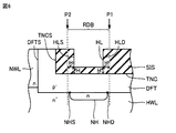
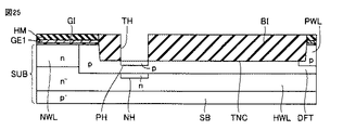
高耐圧CMOSトランジスタのpLDMOSトランジスタについては、図3および図4を用いて以下に説明する。 The pLDMOS transistor of the high breakdown voltage CMOS transistor will be described below with reference to FIGS. 3 and 4.
図3および図4に示されるように、pLDMOSトランジスタの配置領域には、半導体基板SUBの基板領域SB上に、n+埋め込み領域BLが配置されている。そのn+埋め込み領域BL上には、n-ウエル領域HWL(第1ウエル領域)が配置されている。そのn-ウエル領域HWL上には、p-ドリフト領域DFTとn型ウエル領域NWL(第2ウエル領域)とが配置されている。n-ウエル領域HWLは、n型ウエル領域NWLのn型不純物濃度よりも低いn型不純物濃度を有している。 As shown in FIGS. 3 and 4, the n + buried region BL is arranged on the substrate region SB of the semiconductor substrate SUB in the region where the pLDMOS transistor is arranged. An n − well region HWL (first well region) is arranged on the n + buried region BL. A p − drift region DFT and an n-type well region NWL (second well region) are arranged on the n − well region HWL. The n − well region HWL has an n-type impurity concentration lower than that of the n-type well region NWL.
p-ドリフト領域DFTとn型ウエル領域NWLとは、pn接合を構成するように互いに隣り合っている。p-ドリフト領域DFTとn型ウエル領域NWLとにより構成されるpn接合は半導体基板SUBの主表面MSから深さ方向に沿って延びている。 The p − drift region DFT and the n-type well region NWL are adjacent to each other so as to form a pn junction. A pn junction formed by p − drift region DFT and n type well region NWL extends from main surface MS of semiconductor substrate SUB along the depth direction.
半導体基板SUBの主表面MSにはSTIが配置されている。このSTIは、分離溝TNCと、分離絶縁膜SISとを有している。分離溝TNCは、p-ドリフト領域DFTに配置されている。つまりp-ドリフト領域DFTは、分離溝TNCの周囲を取り囲むとともに、分離溝TNCの下側に位置している。分離絶縁膜SISは、分離溝TNCを埋め込んでいる。分離絶縁膜SISの上面には、凹部HLが配置されている。この凹部HLの底面は分離絶縁膜SIS内に位置している。つまり凹部HLの底部はp-ドリフト領域DFTに達していない。 STI is arranged on main surface MS of semiconductor substrate SUB. This STI has a separation trench TNC and a separation insulating film SIS. Isolation trench TNC is arranged in p − drift region DFT. That is, the p − drift region DFT surrounds the periphery of the isolation trench TNC and is located below the isolation trench TNC. The isolation insulating film SIS fills the isolation trench TNC. The recess HL is arranged on the upper surface of the isolation insulating film SIS. The bottom surface of the recess HL is located in the isolation insulating film SIS. That is, the bottom of the recess HL does not reach the p − drift region DFT.
n型ウエル領域NWL内の主表面MSには、p+ソース領域SCと、n+コンタクト領域WCとが配置されている。p+ソース領域SCとn+コンタクト領域WCとは、互いに隣接している。p+ソース領域SCは、n型ウエル領域NWLおよびn+コンタクト領域WCの各々とpn接合を構成している。n+コンタクト領域WCは、n型ウエル領域NWLのn型不純物濃度よりも高いn型不純物濃度を有している。 P + source region SC and n + contact region WC are arranged on main surface MS in n type well region NWL. The p + source region SC and the n + contact region WC are adjacent to each other. The p + source region SC forms a pn junction with each of the n-type well region NWL and the n + contact region WC. The n + contact region WC has an n-type impurity concentration higher than that of the n-type well region NWL.
p-ドリフト領域DFT内の主表面MSには、p+ドレイン領域DCが配置されている。p+ドレイン領域DCは、分離溝TNCに隣接している。p+ドレイン領域DCは、p-ドリフト領域DFTのp型不純物濃度よりも高いp型不純物濃度を有している。p+ドレイン領域DCは、p+ソース領域SCとの間で分離溝TNCを挟んでいる。 P + drain region DC is arranged on main surface MS in p − drift region DFT. The p + drain region DC is adjacent to the isolation trench TNC. The p + drain region DC has a p-type impurity concentration higher than that of the p − drift region DFT. The p + drain region DC and the p + source region SC sandwich the isolation trench TNC.
p+ソース領域SCとp-ドリフト領域DFTとに挟まれる主表面MSの上にゲート絶縁膜GIを介在してゲート電極GEが配置されている。ゲート電極GEは、p+ソース領域SCとp-ドリフト領域DFTとに挟まれる主表面MSと絶縁されながら対向している。 Gate electrode GE is arranged on main surface MS sandwiched between p + source region SC and p − drift region DFT with gate insulating film GI interposed. The gate electrode GE is opposed to the main surface MS sandwiched between the p + source region SC and the p − drift region DFT while being insulated from the main surface MS.
ゲート電極GEは、STIの分離絶縁膜SIS上に乗り上げており、かつ分離絶縁膜SISの凹部HL内を埋め込んでいる。ゲート電極GEは、凹部HL内を埋め込む部分からさらにドレイン領域DC側に延在している。このゲート電極GEは、分離絶縁膜SISを介在してp-ドリフト領域DFTおよびn-ウエル領域HWLの各々と対向している。 The gate electrode GE rides on the isolation insulating film SIS of STI and fills the recess HL of the isolation insulating film SIS. The gate electrode GE further extends to the drain region DC side from the portion that fills the recess HL. This gate electrode GE faces each of p − drift region DFT and n − well region HWL with isolation insulating film SIS interposed.
p-ドリフト領域DFTの下側には、凹部HLの真下に位置する部分を有するようにn型不純物領域NH(第1不純物領域)が配置されている。n型不純物領域NHは、p-ドリフト領域DFTに接していてもよいが、p-ドリフト領域DFTに接していなくてもよい。 Below the p − drift region DFT, an n-type impurity region NH (first impurity region) is arranged so as to have a portion located directly below the recess HL. n-type impurity regions NH is, p - may be in contact with the drift region DFT is, p - may not be in contact with the drift region DFT.
図5に示されるように、n型不純物領域NHは、たとえば1×1017cm-3〜6×1017cm-3のn型不純物濃度CAを有している。一方、n - ウエル領域HWLは、たとえば5×1015cm-3のn型不純物濃度CBを有している。n型不純物領域NHとn - ウエル領域HWLとの境界は、たとえば1×1016cm-3のn型不純物濃度を有する部分である。 As shown in FIG. 5, the n-type impurity region NH has an n-type impurity concentration CA of, for example, 1×10 17 cm −3 to 6×10 17 cm −3 . On the other hand, the n - well region HWL has an n-type impurity concentration CB of, for example, 5×10 15 cm -3 . The boundary between n type impurity region NH and n − well region HWL is a portion having an n type impurity concentration of, for example, 1×10 16 cm −3 .
図6に示されるように、本開示において凹部HLの真下とは、凹部HLの底面から分離溝TNCの底面までの距離Hと同じ寸法Hだけ凹部HLを平面視で拡大した領域RDB(図3の破線で示す領域)内の真下領域を意味する。 As shown in FIG. 6, in the present disclosure, “underneath the recess HL” means an area RDB in which the recess HL is enlarged in plan view by the same dimension H as the distance H from the bottom surface of the recess HL to the bottom surface of the separation groove TNC (FIG. Area indicated by the broken line).
ここで、凹部HLのドレイン領域DC側の端部HLDから上記寸法H分だけドレイン領域DC側の位置を位置P1とする。このとき、n型不純物領域NHのドレイン領域DC側の端部NHDは、位置P1よりもソース領域SC側に位置している。 Here, the position on the drain region DC side by the above dimension H from the end HLD on the drain region DC side of the recess HL is defined as position P1. At this time, the end portion NHD of the n-type impurity region NH on the drain region DC side is located closer to the source region SC than the position P1.
また、凹部HLのソース領域SC側の端部HLSから上記寸法H分だけソース領域SC側の位置を位置P2とする。このとき、n型不純物領域NHのソース領域SC側の端部NHSは、位置P2よりもドレイン領域DC側に位置していることが好ましい。 Further, the position on the source region SC side by the above dimension H from the end HLS on the source region SC side of the concave portion HL is set to the position P2. At this time, the end portion NHS of the n-type impurity region NH on the source region SC side is preferably located closer to the drain region DC than the position P2.
またn型不純物領域NHは凹部HLの真下にのみ位置していることが好ましい。具体的には、n型不純物領域NHは、上記領域RDB内に配置されており、平面視においてこの領域RDBからはみださないことが好ましい。なお平面視とは、たとえば図3に示されるように半導体基板SUBの主表面MSに対して直交する方向から見た視点を意味する。 Further, it is preferable that the n-type impurity region NH is located only directly below the recess HL. Specifically, the n-type impurity region NH is arranged in the region RDB and preferably does not protrude from the region RDB in a plan view. The plan view means a viewpoint as seen from a direction orthogonal to the main surface MS of the semiconductor substrate SUB as shown in FIG. 3, for example.
また、n型不純物領域NHのソース領域SC側の端部NHSは、分離溝TNCのソース領域SC側の端部TNCSよりもドレイン領域DC側に位置している。またn型不純物領域NHのソース領域SC側の端部NHSは、p-ドリフト領域DFTのソース領域SC側の端部DFTSよりもドレイン領域DC側に位置している。 Further, the end portion NHS of the n-type impurity region NH on the source region SC side is located on the drain region DC side of the end portion TNCS of the isolation trench TNC on the source region SC side. The end portion NHS of the n-type impurity region NH on the source region SC side is located on the drain region DC side of the end portion DFTS of the p − drift region DFT on the source region SC side.
しかし図7に示されるように、n型不純物領域NHのソース側端部NHSは、分離溝TNCのソース領域SC側の端部TNCSよりもソース領域SC側に位置していてもよい。またn型不純物領域NHのソース側端部NHSは、p-ドリフト領域DFTのソース領域SC側の端部DFTSよりもソース領域SC側に位置していてもよい。 However, as shown in FIG. 7, the source-side end NHS of the n-type impurity region NH may be located closer to the source region SC than the end TNCS of the isolation trench TNC on the source region SC side. The source-side end NHS of the n-type impurity region NH may be located closer to the source region SC than the end DFTS of the p − drift region DFT on the source region SC side.
図4に示されるように、ソース領域SCからドレイン領域DCへ向かう方向(ソース−ドレイン方向)における分離溝TNCの長さはLdである。凹部HLは、分離溝TNCのソース領域SC側の端部TNCSから、上記長さLdの3分の1の寸法の範囲内に位置している。 As shown in FIG. 4, the length of the isolation trench TNC in the direction from the source region SC to the drain region DC (source-drain direction) is Ld. The recess HL is located within a range of a size of one third of the length Ld from the end TNCS of the isolation trench TNC on the source region SC side.
具体的には、凹部HLのドレイン領域DC側の端部HLDと分離溝TNCのソース領域SC側の端部TNCSとの間の寸法Lhは、上記長さLdの3分の1以下である。 Specifically, the dimension Lh between the end portion HLD of the recess HL on the drain region DC side and the end portion TNCS of the isolation trench TNC on the source region SC side is one third or less of the length Ld.
またn型不純物領域NHも、分離溝TNCのソース領域SC側の端部TNCSから、分離溝TNCの長さLdの3分の1の寸法の範囲内に位置している。 Further, the n-type impurity region NH is also located within a range of one third of the length Ld of the separation trench TNC from the end portion TNCS of the separation trench TNC on the source region SC side.
具体的には、n型不純物領域NHのドレイン領域DC側の端部NHDと分離溝TNCのソース領域SC側の端部TNCSとの間の上記ソース−ドレイン方向の寸法は、上記長さLdの3分の1以下である。 Specifically, the dimension in the source-drain direction between the end portion NHD of the n-type impurity region NH on the drain region DC side and the end portion TNCS of the isolation trench TNC on the source region SC side is equal to the length Ld. It is one third or less.
またn型不純物領域NHのソース領域SC側の端部NHSと分離溝TNCのソース領域SC側の端部TNCSとの間の上記ソース−ドレイン方向の寸法は、上記長さLdの3分の1以下である。 The dimension in the source-drain direction between the end portion NHS of the n-type impurity region NH on the source region SC side and the end portion TNCS of the isolation trench TNC on the source region SC side is one third of the length Ld. It is below.
また凹部HLのソース領域SC側の端部HLSと分離溝TNCのソース領域SC側の端部TNCSとの間の寸法Lsは、ゲート絶縁膜GIの膜厚以上である。 The dimension Ls between the end portion HLS of the recess HL on the source region SC side and the end portion TNCS of the isolation trench TNC on the source region SC side is equal to or larger than the film thickness of the gate insulating film GI.
半導体基板SUBの主表面MS上には、層間絶縁膜ISが配置されている。層間絶縁膜ISには、複数のコンタクトホールCN1、CN2、CN3が配置されている。コンタクトホールCN1は、p+ソース領域SCおよびn+コンタクト領域WCの双方に達している。コンタクトホールCN2は、ゲート電極GEに達している。コンタクトホールCN3は、p+ドレイン領域DCに達している。 Interlayer insulating film IS is arranged on main surface MS of semiconductor substrate SUB. A plurality of contact holes CN1, CN2, CN3 are arranged in the interlayer insulating film IS. Contact hole CN1 reaches both p + source region SC and n + contact region WC. The contact hole CN2 reaches the gate electrode GE. The contact hole CN3 reaches the p + drain region DC.
各コンタクトホールCN1、CN2、CN3の各々には、プラグ導電層PLが埋め込まれている。層間絶縁膜IS上には複数の配線層INCが配置されている。複数の配線層の各々はプラグ導電層PLに接している。 A plug conductive layer PL is embedded in each of the contact holes CN1, CN2, CN3. A plurality of wiring layers INC are arranged on the interlayer insulating film IS. Each of the plurality of wiring layers is in contact with the plug conductive layer PL.
これにより一の配線層INCは、プラグ導電層PLを介在してp+ソース領域SCおよびn+コンタクト領域WCの双方に電気的に接続されている。他の配線層INCは、プラグ導電層PLを介在してゲート電極GEに電気的に接続されている。さらに他の配線層INCは、プラグ導電層PLを介在してp+ドレイン領域DCに電気的に接続されている。 Thus, one wiring layer INC is electrically connected to both p + source region SC and n + contact region WC with plug conductive layer PL interposed. The other wiring layer INC is electrically connected to the gate electrode GE via the plug conductive layer PL. Still another wiring layer INC is electrically connected to p + drain region DC via a plug conductive layer PL.
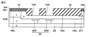
次に、本実施の形態の製造方法について図8〜図15を用いて説明する。
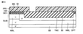
図8に示されるように、p-基板領域SB上にn-ウエル領域HWLが形成される。n-ウエル領域HWL上にn型ウエル領域NWLとp型ドリフト領域DFTとが形成される。これにより、p-基板領域SB、n-ウエル領域HWL、n型ウエル領域NWLおよびp型ドリフト領域DFTを内部に有する半導体基板SUBが準備される。
Next, the manufacturing method according to the present embodiment will be described with reference to FIGS.
As shown in FIG. 8, n − well region HWL is formed on p − substrate region SB. N type well region NWL and p type drift region DFT are formed on n − well region HWL. Thus, the semiconductor substrate SUB having the p − substrate region SB, the n − well region HWL, the n type well region NWL and the p type drift region DFT inside is prepared.
図9に示されるように、半導体基板SUBの主表面上に、たとえばシリコン酸化膜よりなるゲート絶縁膜GIが形成される。ゲート絶縁膜GIは、たとえば数μm〜数十μmの膜厚で形成される。このゲート絶縁膜GI上に、たとえば不純物が導入された多結晶シリコン(ドープドポリシリコン)よりなる導電膜GE1が形成される。この導電膜GE1上に、たとえばシリコン窒化膜よりなるハードマスク層HMが形成される。導電膜GE1およびハードマスク層HMの各々は、たとえば数十nmの膜厚で形成される。 As shown in FIG. 9, a gate insulating film GI made of, for example, a silicon oxide film is formed on the main surface of semiconductor substrate SUB. The gate insulating film GI is formed with a film thickness of, for example, several μm to several tens of μm. On this gate insulating film GI, a conductive film GE1 made of, for example, impurity-doped polycrystalline silicon (doped polysilicon) is formed. A hard mask layer HM made of, for example, a silicon nitride film is formed on this conductive film GE1. Each of the conductive film GE1 and the hard mask layer HM is formed to have a film thickness of several tens nm, for example.
この後、通常の写真製版技術およびエッチング技術によりハードマスク層HMがパターニングされる。このパターニングされたハードマスク層HMをマスクとして、導電膜GE1、ゲート絶縁膜GIおよび半導体基板SUBがエッチングされる。このエッチングにより、半導体基板SUBの主表面MSに分離溝TNCが形成される。 After that, the hard mask layer HM is patterned by the usual photoengraving technique and etching technique. Using the patterned hard mask layer HM as a mask, the conductive film GE1, the gate insulating film GI and the semiconductor substrate SUB are etched. By this etching, isolation trench TNC is formed in main surface MS of semiconductor substrate SUB.
図10に示されるように、分離溝TNC内を埋め込むように、たとえばシリコン酸化膜よりなる絶縁膜BI(埋込絶縁膜)が形成される。この絶縁膜BIの形成においては、たとえば分離溝TNC内を埋め込むように半導体基板SUBの主表面全体上に絶縁膜BIが形成される。この後、たとえばCMP(Chemical Mechanical Polishing)でハードマスク層HMの表面が露出するまで絶縁膜BIが研磨される。これにより、絶縁膜BIが分離溝TNC内のみに残存される。 As shown in FIG. 10, an insulating film BI (buried insulating film) made of, for example, a silicon oxide film is formed so as to fill the inside of the isolation trench TNC. In the formation of insulating film BI, for example, insulating film BI is formed over the entire main surface of semiconductor substrate SUB so as to fill isolation trench TNC. After that, the insulating film BI is polished by, for example, CMP (Chemical Mechanical Polishing) until the surface of the hard mask layer HM is exposed. As a result, the insulating film BI remains only in the isolation trench TNC.
この後、通常の写真製版技術により、フォトレジストパターンPR1が形成される。このフォトレジストパターンPR1は、絶縁膜BIの一部表面を露出する開口を有する。このフォトレジストパターンPR1をマスクとして絶縁膜BIがエッチングされる。このエッチングの後、フォトレジストパターンPR1がたとえばアッシングなどにより除去される。 After that, the photoresist pattern PR1 is formed by a normal photoengraving technique. The photoresist pattern PR1 has an opening that exposes a part of the surface of the insulating film BI. The insulating film BI is etched using the photoresist pattern PR1 as a mask. After this etching, photoresist pattern PR1 is removed by, for example, ashing.
図11に示されるように、上記のエッチングにより絶縁膜BIを貫通してp型ドリフト領域DFTに達する貫通孔THが絶縁膜BIに形成される。この貫通孔THを通じて半導体基板SUBにn型の不純物が注入される。n型不純物のイオン注入の条件は、たとえば注入エネルギーが数百keV〜数MeVで、ドーズ量が1012〜1013cm-2である。このn型不純物の注入により、p型ドリフト領域DFTの下側であって貫通孔THの真下領域にn型不純物領域NHが形成される。 As shown in FIG. 11, a through hole TH that penetrates the insulating film BI and reaches the p-type drift region DFT is formed in the insulating film BI by the above etching. An n-type impurity is injected into the semiconductor substrate SUB through this through hole TH. The conditions for ion implantation of n-type impurities are, for example, an implantation energy of several hundred keV to several MeV and a dose amount of 10 12 to 10 13 cm -2 . By the implantation of the n-type impurity, the n-type impurity region NH is formed in the region below the p-type drift region DFT and directly below the through hole TH.
図12に示されるように、貫通孔THの内壁面を覆い、かつハードマスク層HMおよび絶縁膜BIの各上面を覆うように、たとえばシリコン酸化膜よりなる絶縁膜IL(被覆絶縁膜)が形成される。絶縁膜ILは、たとえば貫通孔THの深さの1/3程度の膜厚で形成される。貫通孔THの内壁面を覆う絶縁膜ILの上面により凹部HLの内壁面が構成される。 As shown in FIG. 12, an insulating film IL (covering insulating film) made of, for example, a silicon oxide film is formed so as to cover the inner wall surface of the through hole TH and the upper surfaces of the hard mask layer HM and the insulating film BI. To be done. The insulating film IL is formed to have a film thickness of about 1/3 of the depth of the through hole TH, for example. The inner wall surface of the recess HL is formed by the upper surface of the insulating film IL that covers the inner wall surface of the through hole TH.
この後、ドープドポリシリコンよりなる導電膜GE2が、凹部HL内を埋め込むように、かつ絶縁膜ILの上面上を覆うように形成される。導電膜GE2は、たとえば数百nmの膜厚で形成される。この後、たとえばCMPで絶縁膜ILの表面が露出するまで導電膜GE2が研磨される。 Then, a conductive film GE2 made of doped polysilicon is formed so as to fill the recess HL and cover the upper surface of the insulating film IL. The conductive film GE2 is formed to have a film thickness of several hundreds nm, for example. After that, the conductive film GE2 is polished by, for example, CMP until the surface of the insulating film IL is exposed.
図13に示されるように、上記のCMPにより凹部HLの内部にのみ導電膜GE2が残存される。この後、絶縁膜ILの一部およびハードマスク層HMがたとえばエッチングにより除去される。 As shown in FIG. 13, the conductive film GE2 remains only inside the recess HL by the above CMP. Then, part of the insulating film IL and the hard mask layer HM are removed by, for example, etching.
図14に示されるように、上記エッチング除去により導電膜GE1の表面が露出する。また上記エッチング除去により絶縁膜ILは貫通孔TH内にのみ残存される。この貫通孔TH内に残存する絶縁膜ILと絶縁膜BIとにより分離絶縁膜SISが形成される。 As shown in FIG. 14, the surface of the conductive film GE1 is exposed by the etching removal. Further, the insulating film IL remains only in the through hole TH by the etching removal. The isolation insulating film SIS is formed by the insulating film IL and the insulating film BI remaining in the through hole TH .
半導体基板SUBの主表面MS上の全面に、たとえばドープドポリシリコンよりなる導電膜GE3が形成される。導電膜GE3は、たとえば数十nmの膜厚で形成される。この後、通常の写真製版技術およびエッチング技術により導電膜GE3、GE1がパターニングされる。これにより、導電膜GE1、GE2、GE3よりなるゲート電極GEが形成される。 A conductive film GE3 made of, for example, doped polysilicon is formed on the entire main surface MS of semiconductor substrate SUB. The conductive film GE3 is formed to have a film thickness of several tens nm, for example. After that, the conductive films GE3 and GE1 are patterned by the usual photoengraving technique and etching technique. As a result, the gate electrode GE made of the conductive films GE1, GE2, and GE3 is formed.
図15に示されるように、ゲート電極GEの側壁に側壁絶縁膜SWが形成される。この後、イオン注入などにより半導体基板SUBの主表面MSにn型不純物およびp型不純物が注入される。これにより半導体基板SUBの主表面MSにp+ソース領域SC、p+ドレイン領域DCおよびn+コンタクト領域WCが形成される。 As shown in FIG. 15, the side wall insulating films SW are formed on the sidewalls of the gate electrode GE. Thereafter, n type impurities and p type impurities are implanted into main surface MS of semiconductor substrate SUB by ion implantation or the like. Thereby, p + source region SC, p + drain region DC and n + contact region WC are formed on main surface MS of semiconductor substrate SUB.
図4に示されるように、層間絶縁膜IS、プラグ導電層PL、配線層INCなどが形成されることにより、本実施の形態の半導体装置が製造される。 As shown in FIG. 4, the semiconductor device of the present embodiment is manufactured by forming the interlayer insulating film IS, the plug conductive layer PL, the wiring layer INC, and the like.
なお、図15における導電膜GE1、GE2、GE3は、図4において1つのゲート電極GEとして示されている。また図15における絶縁膜IL、BIは、図4において1つの分離絶縁膜SISとして示されている。また、図15における側壁絶縁膜SWは図4において省略されている。 Note that the conductive films GE1, GE2, and GE3 in FIG. 15 are shown as one gate electrode GE in FIG. Further, the insulating films IL and BI in FIG. 15 are shown as one isolation insulating film SIS in FIG. Further, the sidewall insulating film SW in FIG. 15 is omitted in FIG.
また図2におけるnLDMOSトランジスタLNTは、上記pLDMOSトランジスタLPTとは逆導電型の構成を有している。具体的には、n+埋め込み領域BL上に、p-ウエル領域HWL(第1ウエル領域)が配置されている。そのp-ウエル領域HWL上には、n-ドリフト領域DFTとp型ウエル領域PWL(第2ウエル領域)とが配置されている。p型ウエル領域PWL内の主表面MSには、n+ソース領域SCと、p+コンタクト領域WCとが形成されている。n-ドリフト領域DFT内の主表面MSには、n+ドレイン領域DCが形成されている。n-ドリフト領域DFTの下側には、凹部HLの真下に位置する部分を有するようにp型不純物領域PH(第1不純物領域)が配置されている。 Further, the nLDMOS transistor LNT in FIG. 2 has a configuration of the opposite conductivity type to the p LD MOS transistor LPT. Specifically, the p − well region HWL (first well region) is arranged on the n + buried region BL. An n − drift region DFT and a p-type well region P WL (second well region) are arranged on the p − well region HWL. N + source region SC and p + contact region WC are formed on main surface MS in p type well region P WL. An n + drain region DC is formed on the main surface MS in the n − drift region DFT. Below the n − drift region DFT, the p-type impurity region PH (first impurity region) is arranged so as to have a portion located directly below the recess HL.
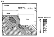
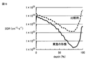
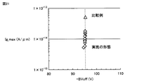
次に、本実施の形態の作用効果について、図4におけるn型不純物領域NHを有しない比較例と対比して説明する。 Next, the function and effect of the present embodiment will be described in comparison with a comparative example having no n-type impurity region NH in FIG.
BiC−DMOS(Bipolar Complementary Metal Oxide Semiconductor)分野においては、図2に示されるように、LDMOSトランジスタ、CMOSトランジスタおよびバイポーラトランジスタが混載される。このような分野においても、デザインスケーリングが進んできている。これにより従来のLOCOS(LoCal Oxidation of Silicon)に代えてSTIが用いられるようになってきている。 In the BiC-DMOS (Bipolar Complementary Metal Oxide Semiconductor) field, as shown in FIG. 2, LDMOS transistors, CMOS transistors and bipolar transistors are mounted together. Even in such fields, design scaling is progressing. As a result, STI has come to be used in place of conventional LOCOS (LoCal Oxidation of Silicon).
この場合、LDMOSトランジスタのドリフト領域にもSTIが用いられることになる。STIにおいては、分離溝のコーナー部の形状がシャープである。このため、ドレインに高電圧が印加された場合に電界が分離溝のコーナー部に集中しやすい。この電界集中により、STIの端部でインパクトイオン化が発生しやすい。インパクトイオン化により発生した電子・ホール対は、界面準位を生成したり、散乱により酸化膜に注入される。これによりホットキャリア変動が大きくなるという問題が顕著になる。特にpLDMOSトランジスタにおいては、ゲート絶縁膜に電子が注入されることによりゲート絶縁膜が絶縁破壊を生じる。 In this case, the STI is also used in the drift region of the LDMOS transistor. In STI, the shape of the corner portion of the separation groove is sharp. Therefore, when a high voltage is applied to the drain, the electric field tends to concentrate on the corner portion of the separation groove. Due to this electric field concentration, impact ionization is likely to occur at the end of the STI. The electron-hole pairs generated by impact ionization generate an interface state or are injected into the oxide film by scattering. As a result, the problem of large hot carrier fluctuation becomes significant. Particularly in a pLDMOS transistor, the gate insulating film causes dielectric breakdown due to injection of electrons into the gate insulating film.
そこで本発明者は、図4における本実施の形態の構成と、図4におけるn型不純物領域NHを有しない比較例の構成とについて、デバイス・シミュレーションによってインパクトイオン化の抑制効果について調べた。その結果を図16および図17に示す。 Therefore, the present inventor investigated the effect of suppressing impact ionization by device simulation for the configuration of the present embodiment in FIG. 4 and the configuration of the comparative example having no n-type impurity region NH in FIG. The results are shown in FIGS. 16 and 17.
図16は比較例における半導体装置のインパクトイオン化率分布を示しており、図17は本実施の形態における半導体装置のインパクトイオン化率分布を示している。この結果から、比較例においては、図16に示すようにSTIのソース領域側の下端においてインパクトイオン化率が高くなっていることがわかる。これに対して本実施の形態においては、図17に示すようにSTIのソース領域側の下端においてインパクトイオン化率が比較例よりも低くなっていることがわかる。 FIG. 16 shows the impact ionization rate distribution of the semiconductor device in the comparative example, and FIG. 17 shows the impact ionization rate distribution of the semiconductor device in the present embodiment. From this result, it can be seen that in the comparative example, as shown in FIG. 16, the impact ionization rate is high at the lower end of the STI on the source region side. On the other hand, in the present embodiment, as shown in FIG. 17, it can be seen that the impact ionization rate at the lower end of the STI on the source region side is lower than that in the comparative example.
また本発明者は、図16および図17の各々のA−A線に沿う電界強度と、インパクトイオン化発生率とを調べた。その結果を図18および図19に示す。 Further, the present inventor examined the electric field intensity along the line AA in FIGS. 16 and 17 and the impact ionization occurrence rate. The results are shown in FIGS. 18 and 19.
図18は図16および図17のA−A線に沿う電界強度を示し、図19は図16および図17のA−A線に沿うインパクトイオン化発生率を示している。図18および図19の結果から、本実施の形態においては比較例よりも電界強度およびインパクトイオン化発生率の双方が低くなっていることがわかる。特にSTIのソース領域側の下端付近において、本実施の形態の電界強度およびインパクトイオン化発生率が、比較例よりも低くなっていることがわかる。 18 shows the electric field strength along the line AA in FIGS. 16 and 17, and FIG. 19 shows the impact ionization occurrence rate along the line AA in FIGS. 16 and 17. From the results of FIGS. 18 and 19, it can be seen that both the electric field strength and the impact ionization occurrence rate are lower in the present embodiment than in the comparative example. In particular, it is understood that the electric field strength and the impact ionization occurrence rate of the present embodiment are lower than those of the comparative example near the lower end of the STI on the source region side.
さらに本発明者は、本実施の形態と比較例との各々におけるオン抵抗Rspとゲート電流Igとの関係と、オフ耐圧BVoffとゲート電流Igとの関係とについて調べた。その結果を図20および図21に示す。 Further, the present inventor investigated the relationship between the on-resistance Rsp and the gate current Ig and the relationship between the off breakdown voltage BVoff and the gate current Ig in each of the present embodiment and the comparative example. The results are shown in FIGS. 20 and 21.
図20は本実施の形態と比較例との各々におけるオン抵抗Rspとゲート電流Igとの関係を示し、図21は本実施の形態と比較例との各々におけるオフ耐圧BVoffとゲート電流Igとの関係を示している。図20および図21の結果から、本実施の形態においては比較例に比べて、オン抵抗Rspが1〜2%増加しているものの、オフ耐圧BVoffを維持したままゲート電流Igを低下できることがわかる。 20 shows the relationship between the on-resistance Rsp and the gate current Ig in each of the present embodiment and the comparative example, and FIG. 21 shows the off breakdown voltage BVoff and the gate current Ig in each of the present embodiment and the comparative example. Shows the relationship. From the results of FIGS. 20 and 21 , it can be seen that in the present embodiment, the on-resistance Rsp is increased by 1 to 2% as compared with the comparative example, but the gate current Ig can be reduced while maintaining the off breakdown voltage BVoff. ..
ここでゲート電流Igとは、半導体基板SUBとゲート電極GEとの間にゲート絶縁膜GIなどを介在して流れる電流のことである。このため、ゲート電流Igが小さいとは、ゲート電極GEに半導体基板SUBから注入されるキャリアの量が少ないことを意味する。よって、ゲート電流Igが低減されるとの上記結果から、本実施の形態では比較例よりもゲート電極GE内へのホットキャリアの注入が抑制できていることがわかる。 Here, the gate current Ig is a current that flows through the gate insulating film GI and the like between the semiconductor substrate SUB and the gate electrode GE. Therefore, the small gate current Ig means that the amount of carriers injected from the semiconductor substrate SUB into the gate electrode GE is small. Therefore, from the above result that the gate current Ig is reduced, it is understood that the injection of hot carriers into the gate electrode GE can be suppressed more in the present embodiment than in the comparative example.
加えて本発明者は、本実施の形態と比較例との各々において、測定素子に対し一定のストレスを与えたときの半導体基板内の電位分布について調べた。その結果を図22および図23に示す。 In addition, the present inventor examined the potential distribution in the semiconductor substrate when a constant stress was applied to the measurement element in each of the present embodiment and the comparative example. The results are shown in FIGS. 22 and 23.
図22は比較例における半導体装置の等電位線を示し、図23は本実施の形態における半導体装置の等電位線を示している。このシミュレーションにおいては、オン耐圧80Vの素子に対し、ゲート電圧Vgを−1.3Vとし、かつドレイン電圧Vdを−80Vとして電位分布を観察した。 22 shows the equipotential lines of the semiconductor device in the comparative example, and FIG. 23 shows the equipotential lines of the semiconductor device in the present embodiment. In this simulation, the potential distribution was observed for an element having an on-breakdown voltage of 80 V, a gate voltage Vg of −1.3 V, and a drain voltage Vd of −80 V.
図22および図23の結果から、比較例においてはSTIのソース領域側の下端において−10Vとなっているのに対し、本実施の形態においてはSTIのソース領域側の下端において−8Vとなっている。また本実施の形態においては、比較例よりもSTIのソース領域側の端部近傍において等電位線の間隔が広がっており、電界が緩和されていることがわかる。 From the results of FIGS. 22 and 23, in the comparative example, the lower end of the STI source region side is −10 V, whereas in the present embodiment, the lower end of the STI source region side is −8 V. There is. Further, in the present embodiment, it can be seen that the electric potential is relaxed because the interval between equipotential lines is wider near the end of the STI on the source region side than in the comparative example.
これらの結果から、本実施の形態においては、n型不純物領域NH(図4)が配置されたことによって、STI端部における電界が緩和され、それによりインパクトイオン化が抑えられたことでホットキャリアのゲート電極GEへの注入がさらに抑制されたと考えられる。 From these results, in the present embodiment, the n-type impurity region NH (FIG. 4) is arranged, so that the electric field at the end of the STI is relaxed, and thereby impact ionization is suppressed, so that hot carrier of the hot carrier is suppressed. It is considered that the injection into the gate electrode GE was further suppressed.
以上より、本実施の形態においては図4に示すようにp型ドリフト領域DFTの下側であって凹部HLの真下領域にn型不純物領域NHが配置されている。このため、上記のとおりオフ耐圧BVoffを維持したままゲート電極GEへのホットキャリアの注入がさらに抑制でき、その結果、ゲート電流Igを抑制することができる。 As described above, in the present embodiment, as shown in FIG. 4, the n-type impurity region NH is arranged below the p-type drift region DFT and directly below the recess HL. Therefore, it is possible to further suppress the injection of hot carriers into the gate electrode GE while maintaining the off breakdown voltage BVoff as described above, and as a result, it is possible to suppress the gate current Ig.
また本実施の形態において凹部HLの真下領域にのみn型不純物領域NHが配置されている場合には、ゲート電極GEへのホットキャリアの注入を抑制しつつ、RESURF(REduced SURface Field)効果により高耐圧を得ることもできる。以下、そのことを説明する。 Further, in the present embodiment, when the n-type impurity region NH is arranged only in the region right below the recess HL, the injection of hot carriers into the gate electrode GE is suppressed and the high effect due to the RESURF (REduced SURface Field) effect. Withstand voltage can also be obtained. This will be described below.
図4の構成において、仮に凹部HLが分離絶縁膜SISに設けられておらず、かつn型不純物領域NHが分離溝TNCの真下領域の全体に配置されている場合について想定する。この場合、n型不純物領域NHが分離溝TNCの真下領域の全体に配置されているため、p-ドリフト領域DFTとn-ウエル領域HWLとの横方向の接合により得られるRESURF効果が得られなくなる。この結果、電界集中が生じやすくなり、耐圧が低下する。 In the configuration of FIG. 4, it is assumed that the recess HL is not provided in the isolation insulating film SIS and the n-type impurity region NH is disposed in the entire region directly below the isolation trench TNC. In this case, since the n-type impurity region NH is arranged in the entire region right below the isolation trench TNC, the RESURF effect obtained by the lateral junction between the p − drift region DFT and the n − well region HWL cannot be obtained. . As a result, electric field concentration is likely to occur and the breakdown voltage decreases.
係る耐圧の低下を抑えるためには、p-ドリフト領域DFTのp型不純物濃度を高くする必要がある。しかしp-ドリフト領域DFTのp型不純物濃度を高くすると、STIの端部近傍での電界集中が促進される。これによりゲート電極GEへのホットキャリアの注入が促進される。 In order to suppress the decrease in breakdown voltage, it is necessary to increase the p-type impurity concentration of the p − drift region DFT. However, if the p-type impurity concentration of the p − drift region DFT is increased, the electric field concentration near the end of the STI is promoted. This accelerates the injection of hot carriers into the gate electrode GE.
これに対して本実施の形態では、凹部HLの真下領域にのみn型不純物領域NHが配置されている。このためp-ドリフト領域DFTとn-ウエル領域HWLとの横方向の接合長さを十分に確保することができる。これにより、RESURF効果によって高耐圧を得ることができる。 On the other hand, in the present embodiment, the n-type impurity region NH is arranged only in the region directly below the recess HL. Therefore, it is possible to secure a sufficient lateral junction length between the p − drift region DFT and the n − well region HWL. As a result, a high breakdown voltage can be obtained by the RESURF effect.
つまり、空乏層がp-ドリフト領域DFTとn-ウエル領域HWLとのpn接合部から上下に拡がり、これにより電界分布が均一化され電界集中が緩和される結果、耐圧が向上する。 That is, the depletion layer spreads vertically from the pn junction between the p − drift region DFT and the n − well region HWL, which makes the electric field distribution uniform and relaxes the electric field concentration, and as a result, the breakdown voltage improves.
また高耐圧を得るためにp-ドリフト領域DFTのp型不純物濃度を高くする必要がない。このためp-ドリフト領域DFTのp型不純物濃度を高くした場合に生じるホットキャリア注入促進も生じない。 Further, it is not necessary to increase the p-type impurity concentration of the p − drift region DFT to obtain a high breakdown voltage. Therefore, promotion of hot carrier injection that occurs when the p-type impurity concentration of the p − drift region DFT is increased does not occur.
以上より、ゲート電極GEへのホットキャリアの注入を抑制しつつ、RESURF効果により高耐圧を得ることもできる。 From the above, it is possible to obtain a high breakdown voltage by the RESURF effect while suppressing the injection of hot carriers into the gate electrode GE.
また本実施の形態においては、n型不純物領域NHは、分離溝TNCのソース領域SC側の端部TNCSから、分離溝TNCの長さLdの3分の1の寸法の範囲内に位置している。このような範囲内にn型不純物領域NHが位置していることにより、上述したRESURF効果による高耐圧を維持することができる。 Further, in the present embodiment, the n-type impurity region NH is located within the range of the dimension of one third of the length Ld of the separation trench TNC from the end portion TNCS of the separation trench TNC on the source region SC side. There is. By positioning the n-type impurity region NH within such a range, it is possible to maintain the high breakdown voltage due to the above-mentioned RESURF effect.
また仮に凹部HLのソース領域SC側の端部HLSと分離溝TNCのソース領域SC側の端部TNCSとの間の寸法Lsがゲート絶縁膜GIの膜厚未満である場合、その薄い分離絶縁膜SISの部分を通過してホットキャリアがゲート電極GEに注入されやすくなる。このため上記寸法Lsがゲート絶縁膜GIの膜厚以上であることにより、その薄い分離絶縁膜SISの部分を通じてゲート電極GEにホットキャリアが注入されることが抑制される。 If the dimension Ls between the end portion HLS of the concave portion HL on the source region SC side and the end portion TNCS of the isolation trench TNC on the source region SC side is less than the film thickness of the gate insulating film GI, the thin isolation insulating film is formed. Hot carriers are easily injected into the gate electrode GE through the SIS portion. Therefore, since the dimension Ls is equal to or larger than the film thickness of the gate insulating film GI, hot carriers are suppressed from being injected into the gate electrode GE through the thin isolation insulating film SIS.
またn型不純物領域NHのソース領域SC側の端部NHSと分離溝TNCのソース領域SC側の端部TNCSとの間の上記ソース−ドレイン方向の寸法が上記分離溝TNCの長さLdの3分の1以下である。これにより、n型不純物領域NHによって、ゲート電極GEへのホットキャリアの注入を十分に抑制することができる。 Further, the dimension in the source-drain direction between the end portion NHS of the n-type impurity region NH on the source region SC side and the end portion TNCS of the isolation trench TNC on the source region SC side is 3 of the length Ld of the isolation trench TNC. It is less than one-third. Thereby, the n-type impurity region NH can sufficiently suppress the injection of hot carriers into the gate electrode GE.
また図6に示されるように、n型不純物領域NHのドレイン領域DC側の端部NHDは、上記位置P1よりもソース領域SC側に位置している。これによりゲート電極GEへのホットキャリアの注入が抑制されるとともに、上記のRESURF効果を得ることができる。 Further, as shown in FIG. 6, the end portion NHD of the n-type impurity region NH on the drain region DC side is located closer to the source region SC than the position P1. As a result, injection of hot carriers into the gate electrode GE is suppressed, and the above RESURF effect can be obtained.
また図4に示されるように、n型ウエル領域NWLよりもn型不純物濃度の低いn+ウエル領域がp+ドリフト領域DFTと横方向に沿って接続されてpn接合を構成している。これにより上記のRESURF効果を得ることができる。 Further, as shown in FIG. 4, an n + well region having a lower n-type impurity concentration than the n-type well region NWL is laterally connected to the p + drift region DFT to form a pn junction. As a result, the above-mentioned RESURF effect can be obtained.
(実施の形態2)
図24に示されるように、本実施の形態の構成は実施の形態1の構成と比較してp型不純物領域PH(第2不純物領域)が追加されている点において異なる。p型不純物領域PHは、p-ドリフト領域DFTよりも高いp型不純物濃度を有している。このp型不純物領域PHは、n型不純物領域NHの濃度ピークよりも低い濃度ピークを有していることが好ましい。
(Embodiment 2)
As shown in FIG. 24, the configuration of the present embodiment is different from that of the first embodiment in that a p-type impurity region PH (second impurity region) is added. The p-type impurity region PH has a p-type impurity concentration higher than that of the p − drift region DFT. The p-type impurity region PH preferably has a concentration peak lower than that of the n-type impurity region NH.
p型不純物領域PHは、凹部HLの真下領域に配置されている。p型不純物領域PHは、p-ドリフト領域DFT内に配置されていれば、分離絶縁膜SISに接していてもよく、また接していなくてもよい。p型不純物領域PHは、n型不純物領域NHと深さ方向に間隔をあけて配置されていることが好ましい。 The p-type impurity region PH is arranged in the region right below the recess HL. The p-type impurity region PH may or may not be in contact with the isolation insulating film SIS as long as it is arranged in the p − drift region DFT. It is preferable that the p-type impurity region PH is arranged at a distance from the n-type impurity region NH in the depth direction.
p型不純物領域PHのドレイン領域DC側の端部PHDは、図6で説明した位置P1よりもソース領域SC側に位置している。p型不純物領域PHのソース領域SC側の端部PHSは、図6で説明した位置P2よりもドレイン領域DC側に位置していることが好ましい。 The end portion PHD of the p-type impurity region PH on the drain region DC side is located closer to the source region SC than the position P1 described in FIG. The end portion PHS of the p-type impurity region PH on the source region SC side is preferably located on the drain region DC side with respect to the position P2 described in FIG.
またp型不純物領域PHは、凹部HLの真下領域のみに配置されていることが好ましい。具体的にはp型不純物領域PHは、平面視において図3で説明した領域RDB内に配置されており、この領域RDBからはみださないことが好ましい。 Further, it is preferable that the p-type impurity region PH is arranged only in the region directly below the recess HL. Specifically, the p-type impurity region PH is arranged in the region RDB described in FIG. 3 in a plan view, and it is preferable that the p-type impurity region PH does not protrude from the region RDB.
またp型不純物領域PHのソース領域SC側の端部PHSは、分離溝TNCのソース領域SC側の端部TNCSよりもドレイン領域DC側に位置している。またp型不純物領域PHのソース領域SC側の端部PHSは、p-ドリフト領域DFTのソース側端部DFTSよりもドレイン領域DC側に位置している。 Further, the end portion PHS of the p-type impurity region PH on the source region SC side is located on the drain region DC side of the end portion TNCS of the isolation trench TNC on the source region SC side. The end portion PHS of the p-type impurity region PH on the source region SC side is located on the drain region DC side of the source-side end portion DFTS of the p − drift region DFT.
しかし図7に示すn型不純物領域NHと同様に、p型不純物領域PHのソース側端部PHSは、分離溝TNCのソース領域SC側の端部TNCSよりもソース領域SC側に位置していてもよい。またp型不純物領域PHのソース側端部PHSは、p-ドリフト領域DFTのソース領域SC側の端部DFTSよりもソース領域SC側に位置していてもよい。 However, like the n-type impurity region NH shown in FIG. 7, the source-side end portion PHS of the p-type impurity region PH is located closer to the source region SC side than the end portion TNCS of the isolation trench TNC on the source region SC side. Good. The source-side end PHS of the p-type impurity region PH may be located closer to the source region SC than the end DFTS of the p − drift region DFT on the source region SC side.
またp型不純物領域PHは、分離溝TNCのソース領域SC側の端部TNCSから、ドリフト領域DFTの長さLdの3分の1の寸法の範囲内に位置している。 Further, the p-type impurity region PH is located within the range of the dimension of one third of the length Ld of the drift region DFT from the end portion TNCS of the isolation trench TNC on the source region SC side.
具体的には、p型不純物領域PHのドレイン領域DC側の端部PHDと分離溝TNCのソース領域SC側の端部TNCSとの間の上記ソース−ドレイン方向の寸法は、上記ドリフト領域DFTの長さLdの3分の1以下である。 Specifically, the dimension in the source-drain direction between the end portion PHD of the p-type impurity region PH on the drain region DC side and the end portion TNCS of the isolation trench TNC on the source region SC side is equal to that of the drift region DFT. It is 1/3 or less of the length Ld.
またp型不純物領域PHのソース領域SC側の端部PHSと分離溝TNCのソース領域SC側の端部TNCSとの間の上記ソース−ドレイン方向の寸法は、上記ドリフト領域DFTの長さLdの3分の1以下である。 The dimension in the source-drain direction between the end portion PHS of the p-type impurity region PH on the source region SC side and the end portion TNCS of the isolation trench TNC on the source region SC side is equal to the length Ld of the drift region DFT. It is one third or less.
なお本実施の形態の上記以外の構成は、上述した実施の形態1の構成をほぼ同じであるため同一の要素については同一の符号を付し、その説明を繰り返さない。 Since the configuration of the present embodiment other than the above is substantially the same as that of the above-described first embodiment, the same elements are designated by the same reference numerals, and the description thereof will not be repeated.
次に、本実施の形態の半導体装置の製造方法について図25を用いて説明する。
本実施の形態の製造方法は、まず図8〜図10に示す実施の形態1の工程と同様の工程を経る。この後、本実施の形態においては図25に示されるように、絶縁膜BIの貫通孔THを通じてn型不純物およびp型不純物が半導体基板SUBに注入される。これにより、n型不純物領域NHとp型不純物領域PHとが半導体基板SUBに形成される。
Next, a method for manufacturing the semiconductor device of this embodiment will be described with reference to FIG.
The manufacturing method of the present embodiment first undergoes the same steps as the steps of the first embodiment shown in FIGS. Then, in the present embodiment, as shown in FIG. 25, n-type impurities and p-type impurities are implanted into semiconductor substrate SUB through through hole TH of insulating film BI. As a result, the n-type impurity region NH and the p-type impurity region PH are formed in the semiconductor substrate SUB.
p型不純物領域PHを形成するためのp型不純物のイオン注入条件は、たとえばエネルギーが数十keVで、ドーズ量が1011〜1012cm-2である。このp型不純物のイオン注入は、注入イオンのノックオンを防ぐため、n型不純物領域NHを形成するためのn型不純物のイオン注入よりも先に行われることが好ましい。 The p-type impurity ion implantation conditions for forming the p-type impurity region PH are, for example, an energy of several tens keV and a dose amount of 10 11 to 10 12 cm −2 . This p-type impurity ion implantation is preferably performed before the n-type impurity ion implantation for forming the n-type impurity region NH in order to prevent knock-on of implanted ions.
この後、本実施の形態の製造方法は、図12〜図15に示す実施の形態1の工程と同様の工程を経る。これにより、図24に示される本実施の形態の半導体装置が製造される。 Thereafter, the manufacturing method of the present embodiment goes through the same steps as the steps of the first embodiment shown in FIGS. As a result, the semiconductor device of this embodiment shown in FIG. 24 is manufactured.
次に、本実施の形態の作用効果について説明する。
本発明者は、本実施の形態におけるオン抵抗Rspおよびゲート電流Igの関係と、オフ耐圧BVoffおよびゲート電流Igの関係とについて調べた。その結果を図26および図27に示す。
Next, the function and effect of this embodiment will be described.
The present inventor investigated the relationship between the on-resistance Rsp and the gate current Ig and the relationship between the off breakdown voltage BVoff and the gate current Ig in the present embodiment. The results are shown in FIGS. 26 and 27.
図26は本実施の形態と実施の形態1と比較例との各々におけるオン抵抗Rspとゲート電流Igとの関係を示している。また図27は本実施の形態と実施の形態1と比較例との各々におけるオフ耐圧BVoffとゲート電流Igとの関係を示している。図26および図27の結果から、本実施の形態においては比較例に比べてゲート電流Igを低減できるとともに、実施の形態1に比べて、オン抵抗Rspをさらに低減できることがわかる。 FIG. 26 shows the relationship between the on-resistance Rsp and the gate current Ig in each of the present embodiment, the first embodiment, and the comparative example. Further, FIG. 27 shows the relationship between the off breakdown voltage BVoff and the gate current Ig in each of the present embodiment, the first embodiment, and the comparative example. From the results of FIGS. 26 and 27, it can be seen that in the present embodiment, the gate current Ig can be reduced as compared with the comparative example, and the on-resistance Rsp can be further reduced as compared with the first embodiment.
以上より、本実施の形態によれば、凹部HLの真下にp型不純物領域PHが追加されたことにより、ゲート電流Igを低減できるとともに、オン抵抗Rspをさらに低減することができる。 As described above, according to the present embodiment, since the p-type impurity region PH is added just below the recess HL, the gate current Ig can be reduced and the on-resistance Rsp can be further reduced.
また仮にp型不純物領域PHがn型不純物領域NHの濃度ピークよりも高い濃度ピークを有する場合、n型不純物領域NHによる電界緩和の効果がp型不純物領域PHにより相殺されるおそれがある。 If the p-type impurity region PH has a concentration peak higher than that of the n-type impurity region NH, the electric field relaxation effect of the n-type impurity region NH may be offset by the p-type impurity region PH.
本実施の形態においては、p型不純物領域PHは、n型不純物領域NHの濃度ピークよりも低い濃度ピークを有している。これによりn型不純物領域NHによる電界緩和の効果がp型不純物領域PHにより相殺されることが抑制される。 In the present embodiment, p-type impurity region PH has a concentration peak lower than that of n-type impurity region NH. This suppresses the effect of the electric field relaxation due to the n-type impurity region NH from being canceled by the p-type impurity region PH.
またp型不純物領域PHのドレイン領域DC側の端部PHDは、凹部HLの底部から分離溝TNCの底部までの深さ方向の寸法H分だけ、凹部HLからドレイン領域DC側へ離れた位置よりもソース領域SC側に位置している。これにより、ゲート電極GEへのホットキャリアの注入が抑制されるとともに、上記のRESURF効果を得ることができる。 Further, the end portion PHD of the p-type impurity region PH on the drain region DC side is located at a position separated from the recess region HL toward the drain region DC side by a dimension H in the depth direction from the bottom of the recess region HL to the bottom of the isolation trench TNC. Is also located on the source region SC side. As a result, injection of hot carriers into the gate electrode GE is suppressed, and the RESURF effect described above can be obtained.
(実施の形態3)
図28に示されるように、本実施の形態の半導体装置は、実施の形態1の構成と比較して、凹部HLが複数個の凹部分HLPを有している点と、n型不純物領域NHが複数個のn型領域部分(第1領域部分)NHPを有している点とにおいて異なっている。
(Embodiment 3)
As shown in FIG. 28, the semiconductor device according to the present embodiment is different from the structure according to the first embodiment in that the recess HL has a plurality of recesses HLP, and the n-type impurity region NH. Has a plurality of n-type region portions (first region portions) NHPs.
複数個の凹部分HLPは、平面視において互いに間隔を隔てて並走するように配置されている。つまり、平面視において複数個の凹部分HLPはいわゆる短冊状に形成されている。複数個の凹部分HLPの各々の幅WAは、複数個の凹部分HLPのうち互いに隣り合う凹部分HLP間の距離WBよりも大きい。 The plurality of recessed portions HLP are arranged so as to run in parallel with each other with a space therebetween in a plan view. That is, the plurality of recessed portions HLP are formed in a so-called strip shape in a plan view. Each width WA of the plurality of recessed portions HLP is larger than the distance WB between the recessed portions HLP adjacent to each other among the plurality of recessed portions HLP.
また複数個のn型領域部分NHPの各々は、互いに間隔を隔てて配置されている。複数個のn型領域部分NHPの各々は、複数個の凹部分HLPの各々の真下領域に配置されている。 In addition, each of the plurality of n-type region portions NHP is arranged at a distance from each other. Each of the plurality of n-type region portions NHP is arranged directly below each of the plurality of recessed portions HLP.
本実施の形態の上記以外の構成は、実施の形態1の構成とほぼ同じであるため、同一の要素については同一の符号を付し、その説明を繰り返さない。 Since the configuration of the present embodiment other than the above is substantially the same as the configuration of the first embodiment, the same elements are designated by the same reference numerals, and the description thereof will not be repeated.
次に、本実施の形態の半導体装置の製造方法について図29〜図33を用いて説明する。なお図29〜図33においては2つの凹部分HLPと2つのn型領域部分が示されているが、図24に示されるように3つの凹部分HLPと3つのn型領域部分が設けられてもよい。 Next, a method of manufacturing the semiconductor device of the present embodiment will be described with reference to FIGS. Although FIGS. 29 to 33 show two recessed portions HLP and two n-type region portions, three recessed portion HLPs and three n-type region portions are provided as shown in FIG. Good.
本実施の形態の製造方法は、まず図8、図9に示す実施の形態1の工程と同様の工程を経る。この後、本実施の形態においては図29に示されるように、通常の写真製版技術により、フォトレジストパターンPR2が形成される。このフォトレジストパターンPR2は、絶縁膜BIの一部表面を露出する開口を有する。このフォトレジストパターンPR2をマスクとして絶縁膜BIがエッチングされる。このエッチングの後、フォトレジストパターンPR2がたとえばアッシングなどにより除去される。 The manufacturing method of the present embodiment first undergoes the same steps as the steps of the first embodiment shown in FIGS. Thereafter, in the present embodiment, as shown in FIG. 29, a photoresist pattern PR2 is formed by a normal photolithography technique. The photoresist pattern PR2 has an opening that exposes a part of the surface of the insulating film BI. The insulating film BI is etched by using the photoresist pattern PR2 as a mask. After this etching, photoresist pattern PR2 is removed by, for example, ashing.
図30に示されるように、上記のエッチングにより絶縁膜BIを貫通してp型ドリフト領域DFTに達する複数の貫通孔部THPが絶縁膜BIに形成される。この複数の貫通孔部THPを通じて半導体基板SUBにn型の不純物が注入される。n型不純物のイオン注入の条件は、たとえば注入エネルギーが数百keV〜数MeVで、ドーズ量が1012〜1013cm-2である。このn型不純物の注入により、複数の貫通孔部THPの各々の真下領域であってp型ドリフト領域DFTの下側に複数のn型領域部分NHPが形成される。複数のn型領域部分NHPによりn型不純物領域NHが構成される。 As shown in FIG. 30, a plurality of through hole portions THP that penetrate the insulating film BI and reach the p-type drift region DFT are formed in the insulating film BI by the above etching. An n-type impurity is injected into the semiconductor substrate SUB through the plurality of through holes THP. The conditions for ion implantation of n-type impurities are, for example, an implantation energy of several hundred keV to several MeV and a dose amount of 10 12 to 10 13 cm -2 . By the implantation of the n-type impurities, a plurality of n-type region portions NHP are formed below the p-type drift region DFT, which are regions directly below the plurality of through-hole portions THP. An n-type impurity region NH is formed by the plurality of n-type region portions NHP.
図31に示されるように、複数の貫通孔部THPの各々の内壁面を覆い、かつハードマスク層HMおよび絶縁膜BIの各上面を覆うように、たとえばシリコン酸化膜よりなる絶縁膜ILが形成される。絶縁膜ILは、たとえば貫通孔部THPの深さの1/3程度の膜厚で形成される。貫通孔部THPの内壁面を覆う絶縁膜ILの上面により凹部分HLPの内壁面が構成される。 As shown in FIG. 31, an insulating film IL made of, for example, a silicon oxide film is formed so as to cover the inner wall surfaces of the plurality of through-hole portions THP and the upper surfaces of the hard mask layer HM and the insulating film BI. To be done. The insulating film IL is formed to have a film thickness of about 1/3 of the depth of the through hole portion THP, for example. The upper surface of the insulating film IL that covers the inner wall surface of the through hole portion THP constitutes the inner wall surface of the recess portion HLP.
この後、ドープドポリシリコンよりなる導電膜GE2が、複数の凹部分HLP内を埋め込むように、かつ絶縁膜ILの上面上を覆うように形成される。導電膜GE2は、たとえば数百nmの膜厚で形成される。この後、たとえばCMPで絶縁膜ILの表面が露出するまで導電膜GE2が研磨される。 Then, a conductive film GE2 made of doped polysilicon is formed so as to fill the insides of the plurality of recesses HLP and cover the upper surface of the insulating film IL. The conductive film GE2 is formed to have a film thickness of several hundreds nm, for example. After that, the conductive film GE2 is polished by, for example, CMP until the surface of the insulating film IL is exposed.
図32に示されるように、上記のCMPにより複数の凹部分HLPの各々の内部にのみ導電膜GE2が残存される。この後、絶縁膜ILの一部およびハードマスク層HMがたとえばエッチングにより除去される。 As shown in FIG. 32, the conductive film GE2 is left only inside each of the plurality of recessed portions HLP by the above CMP. Then, part of the insulating film IL and the hard mask layer HM are removed by, for example, etching.
図33に示されるように、上記エッチング除去により導電膜GE1の表面が露出する。また上記エッチング除去により絶縁膜ILは貫通孔TH内にのみ残存される。この貫通孔IL内に残存する絶縁膜ILと絶縁膜BIとにより分離絶縁膜SISが形成される。 As shown in FIG. 33, the surface of the conductive film GE1 is exposed by the etching removal. Further, the insulating film IL remains only in the through hole TH by the etching removal. The isolation insulating film SIS is formed by the insulating film IL and the insulating film BI remaining in the through hole IL.
半導体基板SUBの主表面MS上の全面に、たとえばドープドポリシリコンよりなる導電膜GE3が形成される。導電膜GE3は、たとえば数十nmの膜厚で形成される。この後、通常の写真製版技術およびエッチング技術により導電膜GE3、GE1がパターニングされる。これにより、導電膜GE1、GE2、GE3よりなるゲート電極GEが形成される。 A conductive film GE3 made of, for example, doped polysilicon is formed on the entire main surface MS of semiconductor substrate SUB. The conductive film GE3 is formed to have a film thickness of several tens nm, for example. After that, the conductive films GE3 and GE1 are patterned by the usual photoengraving technique and etching technique. As a result, the gate electrode GE made of the conductive films GE1, GE2, and GE3 is formed.
この後、本実施の形態の製造方法は、図15に示す実施の形態1の工程と同様の工程を経る。これにより、図28に示されるのと同等の構成を有する本実施の形態の半導体装置が製造される。 Thereafter, the manufacturing method of the present embodiment goes through the same steps as the steps of the first embodiment shown in FIG. As a result, the semiconductor device of the present embodiment having the same structure as that shown in FIG. 28 is manufactured.
次に、本実施の形態の作用効果について図34〜図35に示す比較例と対比して説明する。 Next, the operation and effect of the present embodiment will be described in comparison with the comparative example shown in FIGS. 34 to 35.
比較例においては、図34に示されるように、幅の広い1つの凹部HLが形成される。この場合、導電膜GE2が形成され、図35に示されるように導電膜GE2がエッチバックされると、導電膜GE2は凹部HLを埋め込むことができない。この場合、導電膜GE2は、凹部HLの側壁にのみ、サイドウォール形状で残る。 In the comparative example, as shown in FIG. 34, one wide recess HL is formed. In this case, when the conductive film GE2 is formed and the conductive film GE2 is etched back as shown in FIG. 35, the conductive film GE2 cannot fill the recess HL. In this case, the conductive film GE2 remains in the sidewall shape only on the sidewall of the recess HL.
これに対して本実施の形態においては、図28に示されるように凹部HLが複数の凹部分HLPを有している。このため、1つの凹部分HLPの幅WAを小さくしつつも、複数の凹部分HLP全体の幅(たとえば3×WA+2×WB)を大きく確保することができる。 On the other hand, in this embodiment, as shown in FIG. 28, the recess HL has a plurality of recesses HLP. Therefore, it is possible to secure a large overall width (for example, 3×WA+2×WB) of the plurality of recessed portions HLP while reducing the width WA of one recessed portion HLP.
このためゲート電極GEへのホットキャリアの注入を抑制できながら、各凹部分HLPを導電膜GE2で埋め込むことが可能となる。 Therefore, it is possible to suppress the injection of hot carriers into the gate electrode GE and fill each recess HLP with the conductive film GE2.
また本実施の形態の製造方法においては、実施の形態1と比較して、フォトマスクを追加することなく複数の凹部分HLPを形成することができる。 Further, in the manufacturing method of the present embodiment, a plurality of recessed portions HLP can be formed without adding a photomask, as compared with the first embodiment.
また凹部HLの幅Lt(図1参照)が大きくなると、電界が緩和されて寿命(ΔTTF)が向上する(以下の論文参照)。このため寿命向上の観点からは凹部HLの幅が大きいことが好ましい。 Further, when the width Lt (see FIG. 1) of the recess HL is increased, the electric field is relaxed and the life (ΔTTF) is improved (see the following paper). Therefore, it is preferable that the width of the recess HL is large from the viewpoint of improving the life.
論文:H. Fujii et al., "A Recessed Gate LDMOSFET for Alleviating HCI Effects", Proceedings of the 2016 28th ISPSD, June 12-16, 2016, Prague, Czech Republic, pp.167-170
そこで本実施の形態では、複数の凹部分HLPの各々の幅WAは、複数の凹部分HLPのうちの互いに隣り合う凹部分HLP間の距離WBよりも大きく設定されている。これにより、複数の凹部分HLPの幅WAの合計を可能な限り大きく確保することが可能となり、寿命が向上する。
Paper: H. Fujii et al., "A Recessed Gate LDMOSFET for Alleviating HCI Effects", Proceedings of the 2016 28th ISPSD, June 12-16, 2016, Prague, Czech Republic, pp.167-170
Therefore, in the present embodiment, the width WA of each of the plurality of recessed portions HLP is set to be larger than the distance WB between the mutually adjacent recessed portions HLP of the plurality of recessed portions HLP. As a result, the total width WA of the plurality of recessed portions HLP can be secured as large as possible, and the life is improved.
なお、図36に示されるように、実施の形態3の構成に、p型不純物領域PHが追加されてもよい。p型不純物領域PHは、複数のp型領域部分PHPを有している。複数のp型領域部分PHPの各々は、複数の凹部分HLPの各々の真下領域に配置されている。 As shown in FIG. 36, p-type impurity region PH may be added to the configuration of the third embodiment. The p-type impurity region PH has a plurality of p-type region portions PHP. Each of the plurality of p-type region portions PHP is arranged in a region directly below each of the plurality of recessed portions HLP.
この変形例は、図30に示す実施の形態3の製造工程に代えて、図37に示すようにn型不純物だけでなく、p型不純物も注入することにより製造される。これ以外の上記変形例の製造方法は、実施の形態3とほぼ同じであるため、その説明は繰り返さない。 This modification is manufactured by implanting not only n-type impurities but also p-type impurities as shown in FIG. 37 instead of the manufacturing process of the third embodiment shown in FIG. The manufacturing method of the above modification other than this is almost the same as that of the third embodiment, and therefore the description thereof will not be repeated.
この変形例においては、複数のp型領域部分PHPを有するp型不純物領域PHが追加されることにより、実施の形態2と同様の作用効果を得ることができる。 In this modification, by adding the p-type impurity region PH having a plurality of p-type region portions PHP, it is possible to obtain the same effect as that of the second embodiment.
なお上記の実施の形態1〜3においては、pLDMOSトランジスタについて説明したが、本開示は図38に示すようなnLDMOSトランジスタにも適用することができる。この場合においても上記と同様の作用効果を得ることができる。 Note that, although the pLDMOS transistor is described in the above first to third embodiments, the present disclosure can be applied to the nLDMOS transistor as shown in FIG. 38. Even in this case, the same effect as the above can be obtained.
また上記においてはpLDMOSトランジスタおよびnLDMOSトランジスタについて説明した。しかし、本開示はpLDMIS(Laterally Diffused Metal Insulator Semiconductor)トランジスタまたはnLDMISトランジスタのようにゲート絶縁膜GIがシリコン酸化膜以外の材質のものにも同様に適用することができる。 Further, the pLDMOS transistor and the nLDMOS transistor have been described above. However, the present disclosure can be similarly applied to a material such as a pLDMIS (Laterally Diffused Metal Insulator Semiconductor) transistor or an nLDMIS transistor whose gate insulating film GI is a material other than a silicon oxide film.
以上、本発明者によってなされた発明を実施の形態に基づき具体的に説明したが、本発明は前記実施の形態に限定されるものではなく、その要旨を逸脱しない範囲で種々変更可能であることはいうまでもない。 Although the invention made by the inventor has been specifically described based on the embodiment, the invention is not limited to the embodiment, and various modifications can be made without departing from the scope of the invention. Needless to say.
ANA アナログ回路、BC ベース領域、BIL,IL 絶縁膜、BL n+埋め込み領域、BTR バイポーラトランジスタ、CH 半導体装置、CN,CN1,CN2,CN3 コンタクトホール、DC ドレイン領域、DFT p型ドリフト領域、DFTS,NHS,PHS,TNCS ソース側端部、HLD,NHD,PHD ドレイン側端部、DRI ドライバ回路、DTR 溝、EC エミッタ領域、GE ゲート電極、GE1,GE2,GE3 導電膜、GI ゲート絶縁膜、HL 凹部、HLP 凹部分、HM ハードマスク層、HWL ウエル領域、INC 配線層、IOC 入出力回路、IS 層間絶縁膜、LC ロジック回路、LNT nLDMOSトランジスタ、LPT pLDMOSトランジスタ、MS 主表面、NH n型不純物領域、NHP n型領域部分、NTR nMOSトランジスタ、NWL n型ウエル領域、P1,P2 位置、PC 電源回路、PDR プリドライバ回路、PH p型不純物領域、PHP p型領域部分、PL プラグ導電層、PR1,PR2 フォトレジスト、PTR pMOSトランジスタ、PWL p型ウエル領域、SB 基板領域、SC ソース領域、SIS 分離絶縁膜、SUB 半導体基板、SW 側壁絶縁膜、TH 貫通孔、THP 貫通孔部、TNC 分離溝、WC コンタクト領域。 ANA analog circuit, BC base region, BIL, IL insulating film, BL n + buried region, BTR bipolar transistor, CH semiconductor device, CN, CN1, CN2, CN3 contact hole, DC drain region, DFT p-type drift region, DFTS, NHS, PHS, TNCS source side end, HLD, NHD, PHD drain side end, DRI driver circuit, DTR groove, EC emitter region, GE gate electrode, GE1, GE2, GE3 conductive film, GI gate insulating film, HL recess , HLP concave portion, HM hard mask layer, HWL well region, INC wiring layer, IOC input/output circuit, IS interlayer insulating film, LC logic circuit, LNT nLDMOS transistor, LPT pLDMOS transistor, MS main surface, NH n type impurity region, NHP n-type region portion, NTR nMOS transistor, NWL n-type well region, P1 and P2 positions, PC power supply circuit, PDR pre-driver circuit, PH p-type impurity region, PHP p-type region portion, PL plug conductive layer, PR1 and PR2 Photoresist, PTR pMOS transistor, PWL p-type well region, SB substrate region, SC source region, SIS isolation insulating film, SUB semiconductor substrate, SW sidewall insulating film, TH through hole, THP through hole part, TNC isolation groove, WC contact region.
Claims (11)
前記半導体基板の前記主表面に配置された、第1導電型のソース領域と、
前記ソース領域との間で前記分離溝を挟むように前記主表面に配置された、第1導電型のドレイン領域と、
前記分離溝の下側に位置し、かつ前記ドレイン領域に接続された、第1導電型のドリフト領域と、
前記分離溝内を埋め込み、かつ上面に凹部を有する分離絶縁膜と、
前記ソース領域と前記ドリフト領域とに挟まれる前記主表面に絶縁しながら対向し、かつ前記凹部内を埋め込むゲート電極と、
前記ドリフト領域の下側であって前記凹部の真下に位置する部分を有する、第2導電型の第1不純物領域とを備え、
前記第1不純物領域は前記凹部の真下にのみ位置する、半導体装置。 A semiconductor substrate having a main surface and having a separation groove on the main surface;
A source region of the first conductivity type disposed on the main surface of the semiconductor substrate;
A drain region of the first conductivity type, which is arranged on the main surface so as to sandwich the separation groove between the drain region and the source region;
A drift region of the first conductivity type, which is located below the isolation trench and connected to the drain region;
An isolation insulating film that fills the isolation trench and has a recess on the upper surface;
A gate electrode facing the main surface sandwiched between the source region and the drift region while insulating, and filling the recess.
A first impurity region of a second conductivity type, which has a portion located below the drift region and directly below the recess ,
The semiconductor device according to claim 1, wherein the first impurity region is located just below the recess .
前記第1不純物領域は、前記分離溝の前記ソース領域側の端部から前記長さLdの3分の1の寸法の範囲内に位置している、請求項1に記載の半導体装置。 The length of the drift region in the direction from the source region to the drain region is Ld,
The semiconductor device according to claim 1, wherein the first impurity region is located within a range of a dimension of one-third of the length Ld from an end of the isolation trench on the source region side.
前記ソース領域と前記ドリフト領域との間の前記主表面に位置する第2導電型の第2ウエル領域とをさらに備え、
前記第1ウエル領域は、前記第2ウエル領域よりも低い不純物濃度を有する、請求項1に記載の半導体装置。 A first well region of a second conductivity type located below the drift region,
A second well region of the second conductivity type located on the main surface between the source region and the drift region,
The semiconductor device according to claim 1, wherein the first well region has an impurity concentration lower than that of the second well region.
前記第2不純物領域は、前記複数の凹部分のそれぞれの真下領域に位置する複数の第2領域部分を有している、請求項5に記載の半導体装置。 The recess has a plurality of recesses,
The semiconductor device according to claim 5 , wherein the second impurity region has a plurality of second region portions located directly under regions of the plurality of recesses.
前記第1不純物領域は、前記複数の凹部分のそれぞれの真下領域に位置する複数の第1領域部分を有している、請求項1に記載の半導体装置。 The recess has a plurality of recesses,
The semiconductor device according to claim 1, wherein the first impurity region has a plurality of first region portions located directly under regions of the plurality of recesses.
前記分離溝内を埋め込み、かつ上面に凹部を有する分離絶縁膜を形成する工程と、
前記ドリフト領域の下側であって前記凹部の真下に位置する第2導電型の第1不純物領域を形成する工程と、
前記ソース領域と前記ドリフト領域とに挟まれる前記主表面の上にゲート絶縁膜を挟んで対向し、かつ前記凹部内を埋め込むゲート電極を形成する工程とを備え、
前記上面に前記凹部を有する前記分離絶縁膜を形成する工程は、
前記分離溝内を埋め込む埋込絶縁膜を形成する工程と、
前記埋込絶縁膜を貫通する貫通孔を形成する工程と、
前記貫通孔の内壁を覆う被覆絶縁膜を形成する工程とを有し、
前記第1不純物領域を形成する工程は、前記貫通孔を通じて第2導電型の不純物を前記半導体基板に導入する工程を有する、半導体装置の製造方法。 A separation groove having a main surface and located on the main surface, a first conductivity type source region located on the main surface, and positioned on the main surface so as to sandwich the separation groove between the source region. Forming a semiconductor substrate having a first-conductivity-type drain region and a first-conductivity-type drift region located below the isolation trench and connected to the drain region.
A step of filling the separation groove and forming a separation insulating film having a recess on the upper surface;
Forming a second impurity region of the first impurity region located below the drift region and directly below the recess;
Forming a gate electrode on the main surface sandwiched between the source region and the drift region, the gate electrode being opposed to the main surface with a gate insulating film sandwiched therebetween and filling the recess .
The step of forming the isolation insulating film having the recess on the upper surface,
Forming a buried insulating film filling the isolation trench;
A step of forming a through hole penetrating the embedded insulating film,
And a step of forming a coating insulating film covering the inner wall of the through hole,
The method of manufacturing a semiconductor device , wherein the step of forming the first impurity region includes the step of introducing an impurity of the second conductivity type into the semiconductor substrate through the through hole .
Priority Applications (3)
| Application Number | Priority Date | Filing Date | Title |
|---|---|---|---|
| JP2016246521A JP6710627B2 (en) | 2016-12-20 | 2016-12-20 | Semiconductor device and manufacturing method thereof |
| US15/847,342 US10468523B2 (en) | 2016-12-20 | 2017-12-19 | Semiconductor device and method for manufacturing the same |
| CN201711381037.3A CN108321203B (en) | 2016-12-20 | 2017-12-20 | Semiconductor device and method for manufacturing the same |
Applications Claiming Priority (1)
| Application Number | Priority Date | Filing Date | Title |
|---|---|---|---|
| JP2016246521A JP6710627B2 (en) | 2016-12-20 | 2016-12-20 | Semiconductor device and manufacturing method thereof |
Publications (3)
| Publication Number | Publication Date |
|---|---|
| JP2018101683A JP2018101683A (en) | 2018-06-28 |
| JP2018101683A5 JP2018101683A5 (en) | 2019-05-30 |
| JP6710627B2 true JP6710627B2 (en) | 2020-06-17 |
Family
ID=62556332
Family Applications (1)
| Application Number | Title | Priority Date | Filing Date |
|---|---|---|---|
| JP2016246521A Active JP6710627B2 (en) | 2016-12-20 | 2016-12-20 | Semiconductor device and manufacturing method thereof |
Country Status (3)
| Country | Link |
|---|---|
| US (1) | US10468523B2 (en) |
| JP (1) | JP6710627B2 (en) |
| CN (1) | CN108321203B (en) |
Families Citing this family (8)
| Publication number | Priority date | Publication date | Assignee | Title |
|---|---|---|---|---|
| JP6837384B2 (en) * | 2017-05-23 | 2021-03-03 | ルネサスエレクトロニクス株式会社 | Semiconductor devices and their manufacturing methods |
| US10424647B2 (en) | 2017-10-19 | 2019-09-24 | Texas Instruments Incorporated | Transistors having gates with a lift-up region |
| JP7195167B2 (en) * | 2019-02-08 | 2022-12-23 | ルネサスエレクトロニクス株式会社 | Semiconductor device and method for manufacturing semiconductor device |
| US11195915B2 (en) * | 2019-04-15 | 2021-12-07 | Texas Instruments Incorporated | Semiconductor devices with a sloped surface |
| US11222955B2 (en) * | 2020-04-22 | 2022-01-11 | Wolfspeed, Inc. | Semiconductor power devices having gate dielectric layers with improved breakdown characteristics and methods of forming such devices |
| US11469307B2 (en) * | 2020-09-29 | 2022-10-11 | Taiwan Semiconductor Manufacturing Company, Ltd. | Thicker corner of a gate dielectric structure around a recessed gate electrode for an MV device |
| US20220293729A1 (en) * | 2021-03-11 | 2022-09-15 | Taiwan Semiconductor Manufacturing Company Limited | Field effect transistor including a downward-protruding gate electrode and methods for forming the same |
| TWI828536B (en) * | 2023-02-08 | 2024-01-01 | 力晶積成電子製造股份有限公司 | Transistor structure and manufacturing method thereof |
Family Cites Families (5)
| Publication number | Priority date | Publication date | Assignee | Title |
|---|---|---|---|---|
| JP2003501837A (en) * | 1999-06-03 | 2003-01-14 | コーニンクレッカ フィリップス エレクトロニクス エヌ ヴィ | Semiconductor device including high-voltage circuit element |
| JP2005183633A (en) * | 2003-12-18 | 2005-07-07 | Toyota Central Res & Dev Lab Inc | Semiconductor device and method for manufacturing the same |
| JP5385679B2 (en) * | 2008-05-16 | 2014-01-08 | 旭化成エレクトロニクス株式会社 | Lateral semiconductor device and manufacturing method thereof |
| US9299831B2 (en) * | 2012-10-16 | 2016-03-29 | Asahi Kasei Microdevices Corporation | Field effect transistor and semiconductor device |
| JP6279346B2 (en) * | 2014-02-27 | 2018-02-14 | ルネサスエレクトロニクス株式会社 | Semiconductor device |
-
2016
- 2016-12-20 JP JP2016246521A patent/JP6710627B2/en active Active
-
2017
- 2017-12-19 US US15/847,342 patent/US10468523B2/en active Active
- 2017-12-20 CN CN201711381037.3A patent/CN108321203B/en active Active
Also Published As
| Publication number | Publication date |
|---|---|
| US10468523B2 (en) | 2019-11-05 |
| JP2018101683A (en) | 2018-06-28 |
| US20180175192A1 (en) | 2018-06-21 |
| CN108321203A (en) | 2018-07-24 |
| CN108321203B (en) | 2023-06-30 |
Similar Documents
| Publication | Publication Date | Title |
|---|---|---|
| JP6710627B2 (en) | Semiconductor device and manufacturing method thereof | |
| US8168494B2 (en) | Trench MOS transistor and method of manufacturing the same | |
| US11374124B2 (en) | Protection of drain extended transistor field oxide | |
| KR101531882B1 (en) | Semiconductor device and method for manufacturing the same | |
| US11152505B2 (en) | Drain extended transistor | |
| US9583616B2 (en) | Semiconductor structure including backgate regions and method for the formation thereof | |
| US10910492B2 (en) | Semiconductor device and method for manufacturing the same | |
| JP2006013450A (en) | Semiconductor device and manufacturing method for the same | |
| KR20110078621A (en) | Semiconductor device, and fabricating method thereof | |
| US9054185B2 (en) | Semiconductor device | |
| JP4477309B2 (en) | High breakdown voltage semiconductor device and manufacturing method thereof | |
| JP2013012577A (en) | Semiconductor device | |
| JP2012079742A (en) | Method of manufacturing semiconductor device | |
| JP2014192361A (en) | Semiconductor device and manufacturing method of the same | |
| KR100922557B1 (en) | Method of manufacturing a CMOS transistor and the CMOS transistor | |
| US20180342577A1 (en) | Semiconductor device and method of manufacturing the same | |
| US10950600B2 (en) | Semiconductor device and method of manufacturing the same | |
| US9112013B2 (en) | Semiconductor device and method for producing the same | |
| KR20110079021A (en) | Semiconductor device method for manufacturing the same | |
| JP7201473B2 (en) | Semiconductor device and its manufacturing method | |
| US10672903B2 (en) | Semiconductor device with drain active area | |
| CN114823904A (en) | Semiconductor structure and forming method thereof | |
| KR20100111021A (en) | Semiconductor device and method for manufacturing the same |
Legal Events
| Date | Code | Title | Description |
|---|---|---|---|
| A521 | Request for written amendment filed |
Free format text: JAPANESE INTERMEDIATE CODE: A523 Effective date: 20190419 |
|
| A621 | Written request for application examination |
Free format text: JAPANESE INTERMEDIATE CODE: A621 Effective date: 20190419 |
|
| A131 | Notification of reasons for refusal |
Free format text: JAPANESE INTERMEDIATE CODE: A131 Effective date: 20200128 |
|
| A977 | Report on retrieval |
Free format text: JAPANESE INTERMEDIATE CODE: A971007 Effective date: 20200131 |
|
| A521 | Request for written amendment filed |
Free format text: JAPANESE INTERMEDIATE CODE: A523 Effective date: 20200318 |
|
| TRDD | Decision of grant or rejection written | ||
| A01 | Written decision to grant a patent or to grant a registration (utility model) |
Free format text: JAPANESE INTERMEDIATE CODE: A01 Effective date: 20200519 |
|
| A61 | First payment of annual fees (during grant procedure) |
Free format text: JAPANESE INTERMEDIATE CODE: A61 Effective date: 20200527 |
|
| R150 | Certificate of patent or registration of utility model |
Ref document number: 6710627 Country of ref document: JP Free format text: JAPANESE INTERMEDIATE CODE: R150 |