JP6696552B2 - Wiring capacity canceling method and wiring capacity canceling device - Google Patents
Wiring capacity canceling method and wiring capacity canceling device Download PDFInfo
- Publication number
- JP6696552B2 JP6696552B2 JP2018206982A JP2018206982A JP6696552B2 JP 6696552 B2 JP6696552 B2 JP 6696552B2 JP 2018206982 A JP2018206982 A JP 2018206982A JP 2018206982 A JP2018206982 A JP 2018206982A JP 6696552 B2 JP6696552 B2 JP 6696552B2
- Authority
- JP
- Japan
- Prior art keywords
- sensor
- wiring
- capacitance
- total
- capacitance value
- Prior art date
- Legal status (The legal status is an assumption and is not a legal conclusion. Google has not performed a legal analysis and makes no representation as to the accuracy of the status listed.)
- Active
Links
- 238000000034 method Methods 0.000 title claims description 44
- 230000000295 complement effect Effects 0.000 claims description 159
- 230000008859 change Effects 0.000 claims description 53
- 238000005259 measurement Methods 0.000 claims description 22
- 239000012778 molding material Substances 0.000 claims description 20
- 230000010354 integration Effects 0.000 claims description 8
- 230000000153 supplemental effect Effects 0.000 claims description 3
- 238000010586 diagram Methods 0.000 description 12
- 230000008569 process Effects 0.000 description 12
- 238000000465 moulding Methods 0.000 description 9
- 238000002474 experimental method Methods 0.000 description 8
- 230000007613 environmental effect Effects 0.000 description 7
- 239000000499 gel Substances 0.000 description 6
- FAPWRFPIFSIZLT-UHFFFAOYSA-M Sodium chloride Chemical compound [Na+].[Cl-] FAPWRFPIFSIZLT-UHFFFAOYSA-M 0.000 description 5
- 238000006243 chemical reaction Methods 0.000 description 5
- 239000000463 material Substances 0.000 description 5
- 239000000126 substance Substances 0.000 description 5
- 101100119135 Mus musculus Esrrb gene Proteins 0.000 description 4
- 238000009530 blood pressure measurement Methods 0.000 description 4
- 239000004065 semiconductor Substances 0.000 description 4
- XUIMIQQOPSSXEZ-UHFFFAOYSA-N Silicon Chemical compound [Si] XUIMIQQOPSSXEZ-UHFFFAOYSA-N 0.000 description 3
- 239000003990 capacitor Substances 0.000 description 3
- 238000007667 floating Methods 0.000 description 3
- 239000000047 product Substances 0.000 description 3
- 229910052710 silicon Inorganic materials 0.000 description 3
- 239000010703 silicon Substances 0.000 description 3
- 239000011780 sodium chloride Substances 0.000 description 3
- 229910000679 solder Inorganic materials 0.000 description 3
- 238000004364 calculation method Methods 0.000 description 2
- 239000000919 ceramic Substances 0.000 description 2
- 230000000694 effects Effects 0.000 description 2
- 238000005516 engineering process Methods 0.000 description 2
- 239000000945 filler Substances 0.000 description 2
- 229920001296 polysiloxane Polymers 0.000 description 2
- 238000010521 absorption reaction Methods 0.000 description 1
- 230000009471 action Effects 0.000 description 1
- 239000000853 adhesive Substances 0.000 description 1
- 230000001070 adhesive effect Effects 0.000 description 1
- 230000000712 assembly Effects 0.000 description 1
- 238000000429 assembly Methods 0.000 description 1
- 230000008901 benefit Effects 0.000 description 1
- 230000036772 blood pressure Effects 0.000 description 1
- 210000001124 body fluid Anatomy 0.000 description 1
- 239000010839 body fluid Substances 0.000 description 1
- 238000003169 complementation method Methods 0.000 description 1
- 239000002131 composite material Substances 0.000 description 1
- 239000004020 conductor Substances 0.000 description 1
- 230000003247 decreasing effect Effects 0.000 description 1
- 230000001419 dependent effect Effects 0.000 description 1
- 238000001514 detection method Methods 0.000 description 1
- 229910003460 diamond Inorganic materials 0.000 description 1
- 239000010432 diamond Substances 0.000 description 1
- 239000003989 dielectric material Substances 0.000 description 1
- 239000012530 fluid Substances 0.000 description 1
- 239000004615 ingredient Substances 0.000 description 1
- 239000012212 insulator Substances 0.000 description 1
- 238000004519 manufacturing process Methods 0.000 description 1
- 238000012536 packaging technology Methods 0.000 description 1
- 238000012545 processing Methods 0.000 description 1
- 230000001681 protective effect Effects 0.000 description 1
- 239000012266 salt solution Substances 0.000 description 1
- 239000002210 silicon-based material Substances 0.000 description 1
- 238000005476 soldering Methods 0.000 description 1
- 239000000758 substrate Substances 0.000 description 1
- 239000013589 supplement Substances 0.000 description 1
- 230000001502 supplementing effect Effects 0.000 description 1
- 238000012360 testing method Methods 0.000 description 1
- XLYOFNOQVPJJNP-UHFFFAOYSA-N water Substances O XLYOFNOQVPJJNP-UHFFFAOYSA-N 0.000 description 1
Images


Classifications
-
- G—PHYSICS
- G01—MEASURING; TESTING
- G01D—MEASURING NOT SPECIALLY ADAPTED FOR A SPECIFIC VARIABLE; ARRANGEMENTS FOR MEASURING TWO OR MORE VARIABLES NOT COVERED IN A SINGLE OTHER SUBCLASS; TARIFF METERING APPARATUS; MEASURING OR TESTING NOT OTHERWISE PROVIDED FOR
- G01D18/00—Testing or calibrating apparatus or arrangements provided for in groups G01D1/00 - G01D15/00
-
- G—PHYSICS
- G01—MEASURING; TESTING
- G01D—MEASURING NOT SPECIALLY ADAPTED FOR A SPECIFIC VARIABLE; ARRANGEMENTS FOR MEASURING TWO OR MORE VARIABLES NOT COVERED IN A SINGLE OTHER SUBCLASS; TARIFF METERING APPARATUS; MEASURING OR TESTING NOT OTHERWISE PROVIDED FOR
- G01D5/00—Mechanical means for transferring the output of a sensing member; Means for converting the output of a sensing member to another variable where the form or nature of the sensing member does not constrain the means for converting; Transducers not specially adapted for a specific variable
- G01D5/12—Mechanical means for transferring the output of a sensing member; Means for converting the output of a sensing member to another variable where the form or nature of the sensing member does not constrain the means for converting; Transducers not specially adapted for a specific variable using electric or magnetic means
- G01D5/14—Mechanical means for transferring the output of a sensing member; Means for converting the output of a sensing member to another variable where the form or nature of the sensing member does not constrain the means for converting; Transducers not specially adapted for a specific variable using electric or magnetic means influencing the magnitude of a current or voltage
- G01D5/24—Mechanical means for transferring the output of a sensing member; Means for converting the output of a sensing member to another variable where the form or nature of the sensing member does not constrain the means for converting; Transducers not specially adapted for a specific variable using electric or magnetic means influencing the magnitude of a current or voltage by varying capacitance
-
- G—PHYSICS
- G01—MEASURING; TESTING
- G01L—MEASURING FORCE, STRESS, TORQUE, WORK, MECHANICAL POWER, MECHANICAL EFFICIENCY, OR FLUID PRESSURE
- G01L27/00—Testing or calibrating of apparatus for measuring fluid pressure
- G01L27/002—Calibrating, i.e. establishing true relation between transducer output value and value to be measured, zeroing, linearising or span error determination
- G01L27/005—Apparatus for calibrating pressure sensors
-
- G—PHYSICS
- G01—MEASURING; TESTING
- G01L—MEASURING FORCE, STRESS, TORQUE, WORK, MECHANICAL POWER, MECHANICAL EFFICIENCY, OR FLUID PRESSURE
- G01L9/00—Measuring steady of quasi-steady pressure of fluid or fluent solid material by electric or magnetic pressure-sensitive elements; Transmitting or indicating the displacement of mechanical pressure-sensitive elements, used to measure the steady or quasi-steady pressure of a fluid or fluent solid material, by electric or magnetic means
- G01L9/02—Measuring steady of quasi-steady pressure of fluid or fluent solid material by electric or magnetic pressure-sensitive elements; Transmitting or indicating the displacement of mechanical pressure-sensitive elements, used to measure the steady or quasi-steady pressure of a fluid or fluent solid material, by electric or magnetic means by making use of variations in ohmic resistance, e.g. of potentiometers, electric circuits therefor, e.g. bridges, amplifiers or signal conditioning
- G01L9/04—Measuring steady of quasi-steady pressure of fluid or fluent solid material by electric or magnetic pressure-sensitive elements; Transmitting or indicating the displacement of mechanical pressure-sensitive elements, used to measure the steady or quasi-steady pressure of a fluid or fluent solid material, by electric or magnetic means by making use of variations in ohmic resistance, e.g. of potentiometers, electric circuits therefor, e.g. bridges, amplifiers or signal conditioning of resistance-strain gauges
-
- G—PHYSICS
- G01—MEASURING; TESTING
- G01L—MEASURING FORCE, STRESS, TORQUE, WORK, MECHANICAL POWER, MECHANICAL EFFICIENCY, OR FLUID PRESSURE
- G01L9/00—Measuring steady of quasi-steady pressure of fluid or fluent solid material by electric or magnetic pressure-sensitive elements; Transmitting or indicating the displacement of mechanical pressure-sensitive elements, used to measure the steady or quasi-steady pressure of a fluid or fluent solid material, by electric or magnetic means
- G01L9/12—Measuring steady of quasi-steady pressure of fluid or fluent solid material by electric or magnetic pressure-sensitive elements; Transmitting or indicating the displacement of mechanical pressure-sensitive elements, used to measure the steady or quasi-steady pressure of a fluid or fluent solid material, by electric or magnetic means by making use of variations in capacitance, i.e. electric circuits therefor
-
- G—PHYSICS
- G01—MEASURING; TESTING
- G01N—INVESTIGATING OR ANALYSING MATERIALS BY DETERMINING THEIR CHEMICAL OR PHYSICAL PROPERTIES
- G01N27/00—Investigating or analysing materials by the use of electric, electrochemical, or magnetic means
- G01N27/02—Investigating or analysing materials by the use of electric, electrochemical, or magnetic means by investigating impedance
- G01N27/22—Investigating or analysing materials by the use of electric, electrochemical, or magnetic means by investigating impedance by investigating capacitance
- G01N27/228—Circuits therefor
-
- G—PHYSICS
- G01—MEASURING; TESTING
- G01N—INVESTIGATING OR ANALYSING MATERIALS BY DETERMINING THEIR CHEMICAL OR PHYSICAL PROPERTIES
- G01N27/00—Investigating or analysing materials by the use of electric, electrochemical, or magnetic means
- G01N27/02—Investigating or analysing materials by the use of electric, electrochemical, or magnetic means by investigating impedance
- G01N27/22—Investigating or analysing materials by the use of electric, electrochemical, or magnetic means by investigating impedance by investigating capacitance
- G01N27/223—Investigating or analysing materials by the use of electric, electrochemical, or magnetic means by investigating impedance by investigating capacitance for determining moisture content, e.g. humidity
Landscapes
- Physics & Mathematics (AREA)
- General Physics & Mathematics (AREA)
- Chemical & Material Sciences (AREA)
- Analytical Chemistry (AREA)
- Health & Medical Sciences (AREA)
- Electrochemistry (AREA)
- Chemical Kinetics & Catalysis (AREA)
- Life Sciences & Earth Sciences (AREA)
- Biochemistry (AREA)
- General Health & Medical Sciences (AREA)
- Immunology (AREA)
- Pathology (AREA)
- Measuring Fluid Pressure (AREA)
Description
本発明は、容量センサに関連した方法に関する。具体的には、本発明は、環境状況に起因する容量センサの配線容量を打ち消す方法、および、このような方法を行うように構成された装置に関する。 The present invention relates to methods associated with capacitive sensors. Specifically, the present invention relates to a method of canceling the wiring capacitance of a capacitance sensor due to environmental conditions, and a device configured to perform such a method.
容量センサとは、様々な物理量を検出するように構成されたセンサのことを指す。測定物理量によってセンサの静電容量に変化が生じ、この容量変化を、電子回路で検出して、例えばデジタルデータに変換することが可能である。容量センサの例として、容量性の圧力センサ、加速度計、湿度センサ、化学センサなどがある。 Capacitive sensor refers to a sensor configured to detect various physical quantities. The capacitance of the sensor changes due to the measured physical quantity, and this capacitance change can be detected by an electronic circuit and converted into, for example, digital data. Examples of capacitive sensors include capacitive pressure sensors, accelerometers, humidity sensors, chemical sensors and the like.
容量センサデバイスでは、センサ回路が出力する容量値の解析を行う回路からの配線によって、さらなる平行容量が取り込まれることが多く、この平行容量は、温度や湿度などの環境状況に左右される可能性がある。この配線容量は、検出した容量値に重大な誤差を引き起こす可能性があるので、容量センサによって測定される物理量の検出にも誤差が生じる。一般的に用いられる多くの誘電体は、環境状況の変化に対して非常に不安定である。例えば、環境中の流体からの保護に優れているシリコンゲルは、非常に多くの水分を吸収する。それにより、シリコンゲルの比誘電率は変わるであろう。物質の比誘電率は、その誘電率で表される。そのため、比誘電率の変化は、誘電率の変化で示される。例示したシリコンゲルのような、いくつかの物質では、吸湿の影響およびそれによって引き起こされる誘電率の変化がかなり急速であり、数分から数時間までさまざまである。他の物質では、誘電率の変化がずっと遅いかもしれない。環境状況の変化によって、見かけの全センサ容量は変化し、この変化は、気圧または血圧など、センサが測定することになっている物理量の変化と区別することができない。 In capacitive sensor devices, additional parallel capacitance is often captured by wiring from the circuit that analyzes the capacitance value output by the sensor circuit, and this parallel capacitance may be affected by environmental conditions such as temperature and humidity. There is. Since the wiring capacitance may cause a significant error in the detected capacitance value, an error also occurs in the detection of the physical quantity measured by the capacitance sensor. Many commonly used dielectrics are very unstable with respect to changing environmental conditions. For example, silicone gels, which offer excellent protection from environmental fluids, absorb very much water. This will change the relative permittivity of the silicon gel. The relative permittivity of a substance is represented by its permittivity. Therefore, the change in the relative dielectric constant is indicated by the change in the dielectric constant. For some materials, such as the exemplified silicone gels, the effect of moisture absorption and the resulting change in dielectric constant is fairly rapid, varying from minutes to hours. For other materials, the change in dielectric constant may be much slower. Changes in environmental conditions change the apparent total sensor capacity, which is indistinguishable from changes in physical quantities that the sensor is supposed to measure, such as barometric pressure or blood pressure.
配線容量を別々に測定できれば、配線容量を全センサ容量から差し引き、センサ測定値の精度を維持することができるのは明らかである。しかしながら、センサを配線から切り離して再び接続することをせずに、構造体内部に配置された特定の配線の正確な値を測定することは不可能であり、これは、実際問題としてあまりにも面倒で、配線容量をさらに変化させる可能性もある。 Obviously, if the wiring capacitance can be measured separately, the wiring capacitance can be subtracted from the total sensor capacitance and the accuracy of the sensor measurement value can be maintained. However, it is impossible to measure the exact value of a particular wire placed inside the structure without disconnecting the sensor from the wire and reconnecting it, which is too much of a practical problem. Therefore, the wiring capacitance may be further changed.
[関連技術]
関連技術分野では、特別な遮蔽配置によって配線容量を最小限にすることが多い。
[Related technology]
In the related art, wiring capacitance is often minimized by special shielding arrangements.
特許文献1では、基板上の接続配線跡も遮蔽するのに用いることができる遮蔽方法について開示している。この方法では、導体および絶縁体の多層膜が遮蔽に必要であり、この多層膜は、非常に薄くて非常に高い柔軟性が要求される組立品には適用できないかもしれない。 Patent Document 1 discloses a shielding method that can be used to shield traces of connection wiring on a substrate. This method requires a multilayer film of conductors and insulators for shielding, which may not be applicable to assemblies that are very thin and require very high flexibility.
本発明の目的は、比誘電率の変化による容量センサとインターフェース回路との間の配線容量の変化を、特別な遮蔽層を用いずに打ち消すという課題を解決するような方法および装置を提供することである。 An object of the present invention is to provide a method and apparatus for solving the problem of canceling the change in the wiring capacitance between the capacitance sensor and the interface circuit due to the change in the relative dielectric constant without using a special shielding layer. Is.
本発明の目的は、請求項1の特徴部分に係る方法によって実現される。さらに、本発明の目的は、請求項11の特徴部分に係る装置によっても実現される。
The object of the invention is realized by a method according to the characterizing part of claim 1. Furthermore, the object of the invention is also realized by a device according to the characterizing part of
本発明の好適な実施の形態は、従属請求項において開示される。 Preferred embodiments of the invention are disclosed in the dependent claims.
本発明は、センサ配線の周囲における比誘電率の変化による、センサ配線における配線容量の変化量を十分に補完できるようにする補完配線を導入するという考えに基づく。補完配線容量値を取得し、重み係数を決定する。この重み係数を用いて補完配線容量値と掛け合わせた後、取得した全センサ容量値から乗算後の補完配線容量値を差し引いて、補完済センサ容量値を得る。 The present invention is based on the idea of introducing a complementary wiring that can sufficiently complement the amount of change in the wiring capacitance in the sensor wiring due to the change in the relative dielectric constant around the sensor wiring. The complementary wiring capacitance value is acquired and the weighting coefficient is determined. After using this weighting factor to multiply the complementary wiring capacitance value, the multiplied complementary wiring capacitance value is subtracted from the acquired total sensor capacitance values to obtain the supplemented sensor capacitance value.
本発明の利点は、センサ配線容量に起因するいかなる誤差も、容量センサの出力信号から実質的に取り除くことが可能になることである。これにより、容量センサを用いてなされたセンサ結果は、精度が向上する。 An advantage of the present invention is that any error due to sensor wire capacitance can be substantially removed from the output signal of the capacitance sensor. This improves the accuracy of the sensor results made using the capacitive sensor.
第1の態様によれば、容量センサが出力する容量センサ測定値上の配線容量変化の影響を打ち消す方法を提供する。前記容量センサは、センサ配線と補完配線とを含む少なくとも2つの配線を有するインターフェース回路に接続されている。 According to the first aspect, there is provided a method of canceling the influence of the change in wiring capacitance on the capacitance sensor measurement value output by the capacitance sensor. The capacitance sensor is connected to an interface circuit having at least two wirings including a sensor wiring and a complementary wiring.
当該方法は、前記容量センサから全センサ容量値を取得し、前記補完配線から全補完配線容量値を取得し、取得した前記全センサ容量値から、取得した前記全補完配線容量値であって、重み係数をかけあわせた前記全補完配線容量値を差し引くことによって、補完済センサ容量値を算出し、前記インターフェース回路の出力端子において前記補完済センサ容量値に対応する電気信号を出力する。前記補完済センサ容量値は、前記容量センサと前記インターフェース回路とその配線との周囲環境における比誘電率の変化に依存しない。 The method obtains all sensor capacitance values from the capacitance sensor, obtains all complementary wiring capacitance values from the complementary wiring, from the obtained all sensor capacitance value, the obtained all complementary wiring capacitance value, The complemented sensor capacitance value is calculated by subtracting the total complemented wiring capacitance value multiplied by the weighting coefficient, and an electric signal corresponding to the complemented sensor capacitance value is output at the output terminal of the interface circuit. The complemented sensor capacitance value does not depend on changes in the relative permittivity in the surrounding environment of the capacitance sensor, the interface circuit and the wiring thereof.
第2の態様によれば、前記方法は、さらに、前記全補完配線容量値を取得するために前記センサ配線のすぐそばに配置された前記補完配線に前記インターフェース回路を接続し、前記補完配線は前記インターフェース回路にのみ電気接続される。 According to a second aspect, the method further comprises connecting the interface circuit to the complementary wiring arranged in the immediate vicinity of the sensor wiring to obtain the total complementary wiring capacitance value, and the complementary wiring is It is electrically connected only to the interface circuit.
第3の態様によれば、前記方法は、さらに、前記インターフェース回路の第1入力端子において前記センサ配線が接合され、前記インターフェース回路の第2入力端子において共通配線が接合される場合、前記インターフェース回路によって前記全センサ容量値を取得し、前記インターフェース回路の第1入力端子において前記補完配線が接合され、前記インターフェース回路の第2入力端子において前記共通配線が接合される場合、前記インターフェース回路によって前記全補完配線容量値を取得する。 According to a third aspect, the method further comprises the interface circuit when the sensor wire is joined at a first input terminal of the interface circuit and a common wire is joined at a second input terminal of the interface circuit. When the total sensor capacitance value is obtained by the above, and the complementary wiring is joined at the first input terminal of the interface circuit and the common wiring is joined at the second input terminal of the interface circuit, Get complementary wiring capacitance value.
第4の態様によれば、前記方法は、さらに、前記全センサ配線容量値を取得するための前記センサ配線と、前記全補完配線容量値を取得するための前記補完配線とのうちのいずれか一つに接続されるように前記インターフェース回路の第1入力端子を多重化する。前記多重化は、10ミリ秒から10分の範囲における頻度で発生する。 According to a fourth aspect, the method further includes any one of the sensor wiring for obtaining the total sensor wiring capacitance value and the complementary wiring for obtaining the total complementary wiring capacitance value. The first input terminals of the interface circuit are multiplexed so that they are connected together. The multiplexing occurs with a frequency in the range of 10 ms to 10 minutes.
第5の態様によれば、前記方法は、さらに、前記インターフェース回路の第1入力端子において積分ベース容量のみが接合され、前記インターフェース回路の第2入力端子において共通配線が接合される場合、前記インターフェース回路によって積分ベース容量値を取得し、前記インターフェース回路の第1入力端子において前記センサ配線が接合され、前記インターフェース回路の第2入力端子において前記共通配線が接合される場合、前記インターフェース回路によって、前記積分ベース容量値を含む前記全センサ容量値を取得し、前記インターフェース回路の第1入力端子において前記補完配線が接合され、前記インターフェース回路の第2入力端子において前記共通配線が接合される場合、前記インターフェース回路によって、前記積分ベース容量値を含む前記全補完配線容量値を取得する。前記方法は、さらに、前記補完済センサ容量値を算出する前に、前記積分ベース容量値を前記全センサ配線容量値と前記全補完配線容量値の両方から差し引く。 According to a fifth aspect, the method further comprises: if only the integration base capacitance is joined at the first input terminal of the interface circuit and the common line is joined at the second input terminal of the interface circuit. When the integrated base capacitance value is obtained by a circuit, the sensor wiring is joined at the first input terminal of the interface circuit, and the common wiring is joined at the second input terminal of the interface circuit, the interface circuit When all the sensor capacitance values including an integrated base capacitance value are acquired, the complementary wiring is joined at the first input terminal of the interface circuit, and the common wiring is joined at the second input terminal of the interface circuit, By the interface circuit, Comprising said partial base capacitance value to obtain the total complement wiring capacitance. The method further subtracts the integrated base capacitance value from both the total sensor wiring capacitance value and the total complementary wiring capacitance value before calculating the supplemented sensor capacitance value.
第6の態様によれば、前記方法は、さらに、前記全センサ配線容量値を取得するための前記センサ配線と、前記全補完配線容量値を取得するための前記補完配線と、前記積分ベース容量値を取得するための前記積分ベース容量とのうちのいずれか一つに接続されるように前記インターフェース回路の第1入力端子を多重化する。前記多重化は、10ミリ秒から10分の範囲における頻度で発生する。 According to a sixth aspect, the method further comprises the sensor wiring for obtaining the total sensor wiring capacitance value, the complementary wiring for obtaining the total complementary wiring capacitance value, and the integral base capacitance. The first input terminal of the interface circuit is multiplexed so as to be connected to any one of the integration base capacitance for obtaining a value. The multiplexing occurs with a frequency in the range of 10 ms to 10 minutes.
第7の態様によれば、前記方法は、さらに、前記補完配線と前記共通配線との間の容量が前記センサ配線と前記共通配線との間の容量と実質的に等しくなるように、前記補完配線を配置する。 According to a seventh aspect, the method further comprises the supplementing such that the capacitance between the complementary wiring and the common wiring is substantially equal to the capacitance between the sensor wiring and the common wiring. Place the wiring.
第8の態様によれば、前記方法は、さらに、前記重み係数を、第1測定において、第1全センサ容量値と第1全補完配線容量値とを測定するステップと、前記容量センサと前記容量センサの配線とを、それらの周囲環境における比誘電率の変化にさらすステップと、前記容量センサと前記容量センサの配線とを、それらの周囲環境における前記比誘電率の変化にさらした後、第2測定において、第2全センサ容量値と第2全補完配線容量値とを測定するステップと、前記第1全センサ容量値と前記第2全センサ容量値との間の変化に基づいて、測定した全センサ容量の変化を算出し、前記第1全補完配線容量値と前記第2全補完配線容量値との間の変化に基づいて、測定した全補完配線容量の変化を算出するステップと、前記測定した全センサ容量の変化を前記測定した全補完配線容量の変化で割ることにより前記重み係数を算出するステップとによって取得する。 According to an eighth aspect, the method further comprises: measuring the weighting factor in the first measurement with a first total sensor capacitance value and a first total complementary wiring capacitance value; Exposing the capacitance sensor wiring to changes in the relative permittivity in their ambient environment, and exposing the capacitance sensor and the capacitance sensor wiring to the change in the relative permittivity in their ambient environment, In the second measurement, the step of measuring the second total sensor capacitance value and the second total complementary wiring capacitance value, and the change between the first total sensor capacitance value and the second total sensor capacitance value, Calculating a change in the measured total sensor capacitance and calculating a change in the measured total complementary wiring capacitance based on the change between the first total complementary wiring capacitance value and the second total complementary wiring capacitance value; , All the measured sensor Be obtained by calculating the weight coefficient divided by the change in the total complement wiring capacitance that the measured change in capacitance.
第9の態様によれば、前記方法は、さらに、前記重み係数を、校正関数を定義するステップと、第1全センサ容量値と、第1全補完容量値と、第1基準圧力値とを測定するステップと、ダミー重み係数を用いて、前記第1全センサ容量値と前記第1全補完容量値とに基づいて、第1補完済センサ容量値を算出するステップと、前記校正関数を用いて、前記第1補完済センサ容量値に対応する第1圧力値を算出するステップと、前記容量センサと前記容量センサの配線とを、それらの周囲環境における比誘電率の変化にさらすステップと、前記容量センサと前記容量センサの配線とをそれらの周囲環境における前記比誘電率の変化にさらした後、第2全センサ容量値と、第2全補完容量値と、第2基準圧力値とを測定するステップと、前記第2全センサ容量値と前記第2全補完容量値とに基づいて、第2補完済センサ容量値を算出するステップと、前記校正関数を用いて、前記第2補完済センサ容量値に基づいて第2圧力値を算出するステップと、調節後の前記重み係数を用いて算出される第1圧力誤差が、同じ調節後の前記重み係数を用いて算出される第2圧力誤差と等しくなるように、前記第1補完済センサ容量値と前記第2補完済センサ容量値と前記第1圧力値と前記第2圧力値とを算出するのに用いられる前記重み係数を調節することにより前記重み係数を取得するステップとによって取得し、前記第1圧力誤差は、調節後の前記重み係数を用いて算出される前記第1圧力値と前記第1基準圧力値との差に等しく、前記第2圧力誤差は、調節後の前記重み係数を用いて算出される前記第2圧力値と前記第2基準圧力値との差に等しい。 According to a ninth aspect, the method further comprises defining a calibration function for the weighting factor, a first total sensor capacitance value, a first total complementary capacitance value, and a first reference pressure value. Measuring, using a dummy weighting factor, calculating a first complemented sensor capacitance value based on the first total sensor capacitance value and the first total complementary capacitance value; and using the calibration function. Calculating a first pressure value corresponding to the first complemented sensor capacitance value, and exposing the capacitance sensor and the wiring of the capacitance sensor to changes in the relative dielectric constant in their ambient environment, After exposing the capacitance sensor and the wiring of the capacitance sensor to the change in the relative dielectric constant in their surrounding environment, the second total sensor capacitance value, the second total complementary capacitance value, and the second reference pressure value are Measuring step, and the second Calculating a second supplemented sensor capacitance value based on the sensor capacitance value and the second total supplemental capacitance value; and using the calibration function, a second pressure based on the second supplemented sensor capacitance value. A step of calculating a value, and the first pressure error calculated using the adjusted weighting coefficient is equal to the second pressure error calculated using the same adjusted weighting coefficient. 1 obtaining the weighting factor by adjusting the weighting factor used to calculate the complemented sensor capacitance value, the second supplemented sensor capacitance value, the first pressure value and the second pressure value. And the first pressure error is equal to the difference between the first pressure value calculated using the adjusted weighting factor and the first reference pressure value, and the second pressure error is adjusted by Calculated using the weighting factor That is equal to the difference between the second pressure value and the second reference pressure value.
第1の装置態様によれば、容量センサ測定値上の配線容量変化の影響を打ち消すように構成された装置を提供する。当該装置は、少なくとも容量センサとインターフェース回路とを備える。前記容量センサは、センサ配線と補完配線とを含む少なくとも2つの配線を有する前記インターフェース回路に接続されている。当該装置は、前記容量センサから全センサ容量値を取得し、前記補完配線から全補完配線容量値を取得し、取得した前記全センサ容量値から、重み係数をかけ合わせた取得した前記全補完配線容量値を差し引くことによって、補完済センサ容量値を算出し、前記インターフェース回路の出力端子において前記補完済センサ容量値に対応する電気信号を出力するように構成される。前記補完済センサ容量値は、前記容量センサと前記インターフェース回路とその配線との周囲環境における比誘電率の変化に依存しない。 According to a first device aspect, there is provided a device configured to counteract the effects of wiring capacitance changes on capacitance sensor measurements. The device includes at least a capacitance sensor and an interface circuit. The capacitance sensor is connected to the interface circuit having at least two wirings including a sensor wiring and a complementary wiring. The apparatus obtains all sensor capacitance values from the capacitance sensor, obtains all complementary wiring capacitance values from the complementary wiring, and obtains all complementary wiring obtained by multiplying a weighting factor from the obtained all sensor capacitance values. The complemented sensor capacitance value is calculated by subtracting the capacitance value, and an electric signal corresponding to the complemented sensor capacitance value is output at the output terminal of the interface circuit. The complemented sensor capacitance value does not depend on changes in the relative permittivity in the surrounding environment of the capacitance sensor, the interface circuit, and the wiring thereof.
第2の装置態様によれば、前記補完配線は、前記センサ配線のすぐそばに配置され、前記インターフェース回路は、前記全補完配線容量値を取得するために前記補完配線に接続されるように構成される。前記補完配線は、前記インターフェース回路にのみ電気接続される。 According to a second device aspect, the complementary wiring is arranged in the immediate vicinity of the sensor wiring, and the interface circuit is connected to the complementary wiring to obtain the total complementary wiring capacitance value. To be done. The complementary wiring is electrically connected only to the interface circuit.
第3の装置態様によれば、前記インターフェース回路の第2入力端子において共通配線が接合される。さらに、当該装置は、前記全センサ配線容量値を取得するための前記センサ配線と、前記全補完配線容量値を取得するための前記補完配線とのうちのいずれか一つに接続されるように前記インターフェース回路の第1入力端子を多重化するよう構成されたスイッチを備える。前記多重化は、10ミリ秒から10分の範囲における頻度で発生する。 According to the third device aspect, the common wiring is joined at the second input terminal of the interface circuit. Further, the device is connected to any one of the sensor wiring for obtaining the total sensor wiring capacitance value and the complementary wiring for obtaining the total complementary wiring capacitance value. A switch configured to multiplex a first input terminal of the interface circuit. The multiplexing occurs with a frequency in the range of 10 ms to 10 minutes.
第4の装置態様によれば、前記インターフェース回路の第2入力端子において共通配線が接合される。さらに、当該装置は、積分ベース容量値を取得するための積分ベース容量のみと、前記積分ベース容量値を含む前記全センサ配線容量値を取得するための前記センサ配線と、前記積分ベース容量値を含む前記全補完配線容量値を取得するための前記補完配線とのうちのいずれか一つに接続されるように前記インターフェース回路の第1入力端子を多重化するよう構成されたスイッチを備える。前記多重化は、10ミリ秒から10分の範囲における頻度で発生する。さらに、当該装置は、前記補完済センサ容量値を算出する前に、前記積分ベース容量値を前記全センサ配線容量値と前記全補完配線容量値の両方から差し引くように構成される。 According to the fourth device aspect, the common wiring is joined at the second input terminal of the interface circuit. Further, the apparatus includes only an integration base capacitance for obtaining an integration base capacitance value, the sensor wiring for obtaining the total sensor wiring capacitance value including the integration base capacitance value, and the integration base capacitance value. A switch configured to multiplex a first input terminal of the interface circuit to be connected to any one of the complementary wirings for obtaining the total complementary wiring capacitance value including the switch. The multiplexing occurs with a frequency in the range of 10 ms to 10 minutes. Further, the apparatus is configured to subtract the integrated base capacitance value from both the total sensor wiring capacitance value and the total complementary wiring capacitance value before calculating the supplemented sensor capacitance value.
第5の装置態様によれば、前記補完配線と前記共通配線との間の容量が前記センサ配線と前記共通配線との間の容量と実質的に等しくなるように、前記補完配線は配置される。 According to the fifth device aspect, the complementary wiring is arranged such that the capacitance between the complementary wiring and the common wiring is substantially equal to the capacitance between the sensor wiring and the common wiring. ..
第6の装置態様によれば、さらに、当該装置は、第1測定において、第1全センサ容量値と第1全補完配線容量値とを測定し、前記容量センサと前記容量センサの配線とをそれらの周囲環境における比誘電率の変化にさらした後、第2測定において、第2全センサ容量値と第2全補完配線容量値とを測定し、前記第1全センサ容量値と前記第2全センサ容量値との間の変化に基づいて、測定した全センサ容量の変化を算出し、前記第1全補完配線容量値と前記第2全補完配線容量値との間の変化に基づいて、測定した全補完配線容量の変化を算出し、前記測定した全センサ容量の変化を前記測定した全補完配線容量の変化で割ることにより前記重み係数を算出するように構成される。 According to the sixth device aspect, the device further measures the first total sensor capacitance value and the first total complementary wiring capacitance value in the first measurement, and connects the capacitance sensor and the wiring of the capacitance sensor. After being exposed to changes in the relative permittivity in their surrounding environment, in the second measurement, the second total sensor capacitance value and the second total complementary wiring capacitance value are measured, and the first total sensor capacitance value and the second total sensor capacitance value are measured. A change in the measured total sensor capacitance is calculated based on the change between the total sensor capacitance value, and based on the change between the first total complementary wiring capacitance value and the second total complementary wiring capacitance value, The weighting coefficient is calculated by calculating the change in the measured total complementary wiring capacitance and dividing the measured change in the total sensor capacitance by the change in the measured total complementary wiring capacitance.
第7の装置態様によれば、さらに、当該装置は、校正関数を定義し、第1全センサ容量値と、第1全補完容量値と、第1基準圧力値とを測定し、ダミー重み係数を用いて、前記第1全センサ容量値と前記第1全補完容量値とに基づいて、第1補完済センサ容量値を算出し、前記校正関数を用いて、前記第1補完済センサ容量値に対応する第1圧力値を算出し、前記容量センサと前記容量センサの配線とをそれらの周囲環境における比誘電率の変化にさらした後、第2全センサ容量値と、第2全補完容量値と、第2基準圧力値とを測定し、前記第2全センサ容量値と前記第2全補完容量値とに基づいて、第2補完済センサ容量値を算出し、前記校正関数を用いて、前記第2補完済センサ容量値に基づいて第2圧力値を算出し、調節後の前記重み係数を用いて算出される第1圧力誤差が、同じ調節後の前記重み係数を用いて算出される第2圧力誤差と等しくなるように、前記第1補完済センサ容量値と前記第2補完済センサ容量値と前記第1圧力値と前記第2圧力値とを算出するのに用いられる前記重み係数を調節することにより前記重み係数を取得するように構成され、前記第1圧力誤差は、調節後の前記重み係数を用いて算出される前記第1圧力値と前記第1基準圧力値との差に等しく、前記第2圧力誤差は、調節後の前記重み係数を用いて算出される前記第2圧力値と前記第2基準圧力値との差に等しい。 According to a seventh apparatus aspect, the apparatus further defines a calibration function, measures a first total sensor capacitance value, a first total complementary capacitance value, and a first reference pressure value, and uses a dummy weighting factor. Is used to calculate a first complemented sensor capacitance value based on the first total sensor capacitance value and the first total complementary capacitance value, and the calibration function is used to calculate the first supplemented sensor capacitance value. After calculating the first pressure value corresponding to, and exposing the capacitance sensor and the wiring of the capacitance sensor to changes in the relative dielectric constant in their surrounding environment, the second total sensor capacitance value and the second total complementary capacitance Value and a second reference pressure value are measured, a second complementary sensor capacity value is calculated based on the second total sensor capacity value and the second total complementary capacity value, and the calibration function is used. , A second pressure value is calculated based on the second complementary sensor capacitance value, and the weight after adjustment is calculated. The first complemented sensor capacitance value and the second complemented value so that the first pressure error calculated using a number is equal to the second pressure error calculated using the same adjusted weighting coefficient. The weighting coefficient is obtained by adjusting the weighting coefficient used to calculate the sensor capacitance value, the first pressure value and the second pressure value, and the first pressure error is adjusted. The second pressure error is equal to the difference between the first pressure value calculated using the subsequent weighting coefficient and the first reference pressure value, and the second pressure error is calculated using the adjusted weighting coefficient. It is equal to the difference between the two pressure values and the second reference pressure value.
以下、本発明について、付随の図面を参照しながら、好適な実施の形態に関してより詳細に説明する。
回路とは、電気信号を受信、生成、または、処理できる電子デバイスのことを指す。 Circuits refer to electronic devices that can receive, generate, or process electrical signals.
センサ配線は、センサを電子回路につなげる。電子回路は、少なくとも、センサから受信したセンサ測定値としても知られるセンサ信号を処理するように構成されてもよい。本発明では、多重化入力端子を有する電子回路においてセンサ配線と入れ替え可能な追加的補完配線があるものとする。また、補完配線は、実際にはどの電子回路も相互接続しないため、ダミー配線と呼ばれてもよい。この補完配線の他端は、何にも接続されておらず、補完配線は、できるだけセンサ配線と類似の大きさで、できるだけセンサ配線と類似の位置に配置すべきである。入力端子を多重化することにより、補完配線の容量値を測定することが可能になる。しかしながら、この補完配線容量は、検出された全センサ容量値から、補完配線容量として差し引くことができない。なぜなら、製品のばらつきを考慮に入れる実際の設計および実装では、補完配線を完全に複製することは決してできないからである。 The sensor wiring connects the sensor to an electronic circuit. The electronic circuitry may at least be configured to process sensor signals, also known as sensor measurements, received from the sensors. In the present invention, it is assumed that there is an additional complementary wiring that can replace the sensor wiring in an electronic circuit having a multiplexed input terminal. Further, since the complementary wiring does not actually interconnect any electronic circuit, it may be called a dummy wiring. The other end of the complementary wiring is not connected to anything, and the complementary wiring should be as large as the sensor wiring and as close to the sensor wiring as possible. By multiplexing the input terminals, the capacitance value of the complementary wiring can be measured. However, this complementary wiring capacitance cannot be subtracted as the complementary wiring capacitance from all the detected sensor capacitance values. This is because, in actual designs and implementations that take product variations into account, complementary wiring can never be completely duplicated.
本発明によれば、検出された全センサ容量から補完配線容量を差し引く前に、補完配線容量に掛け合わせる一定の重み係数を見つけることができる。本発明は、センサ、回路、および、配線付近の中身のない面およびスペースを埋めるのにモールド材を用いることを基本とする。モールド材は、充填材と呼ばれてもよい。モールド材は、空気の誘電率である1より大きい誘電率εrを有することが好ましい。モールドするとセンサ配線容量は変化するので、検出された全センサ容量CStotと検出された補完配線容量CCtotとが変化する。検出された全センサ容量の変化がΔCSで、補完配線容量の変化がΔCCであれば、用いられる適正重み係数は以下のとおりである。 According to the present invention, it is possible to find a constant weighting coefficient to be multiplied by the complementary wiring capacitance before subtracting the complementary wiring capacitance from the total detected sensor capacitance. The invention is based on the use of a molding material to fill empty surfaces and spaces near the sensors, circuits and wires. The molding material may be called a filler. The molding material preferably has a dielectric constant ε r greater than 1, which is the dielectric constant of air. Since the sensor wiring capacitance changes when molded, the total detected sensor capacitance C Stot and the detected complementary wiring capacitance C Ctot change. If the change in the detected total sensor capacitance is ΔC S and the change in the complementary wiring capacitance is ΔC C , the appropriate weighting factors used are as follows.
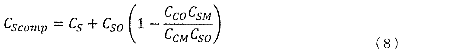
また、補完済センサ容量CScompは以下のとおりである。 Further, the complemented sensor capacitance C Scomp is as follows.
![]()
![]()
このように取得される補完済センサ容量CScompは、基本的に、モールド材の誘電率εrの影響を受けず、配線が適切に設計されていれば、モールド材に起因しない他の配線容量成分も打ち消される。適正重み係数を取得する等価な代替方法で最も簡単な方法は、まず、ダミーの重み係数値k=0もしくはk=1、または、kに対する任意の推測値を用いてセンサを校正し、そして、モールドした前後でセンサが現行圧力に対して同じ圧力誤差を示すように新たなkを選択することである。 The complemented sensor capacitance C Scomp thus obtained is basically not affected by the dielectric constant ε r of the molding material, and if the wiring is properly designed, other wiring capacitance not caused by the molding material. The ingredients are also canceled. The simplest equivalent alternative method of obtaining the proper weighting factor is to first calibrate the sensor with dummy weighting factor values k = 0 or k = 1, or any guess for k, and Choosing a new k so that the sensor shows the same pressure error for the current pressure before and after molding.
以下、配線容量を打ち消す方法について数学的に示す。 Hereinafter, a method of canceling the wiring capacitance will be mathematically shown.
全センサ容量CStotは、センサ容量CSと、モールドキャビティに起因する配線容量CSMと、他の物質に起因する配線容量CSOとの3つの成分の組み合わせとして定義することができる。それに対して、補完配線容量CCtotは、モールドキャビティに起因する配線容量CCMと、他の物質に起因する配線容量CCOとの2つの成分の組み合わせとして定義されてもよい。 The total sensor capacitance C Stot can be defined as a combination of three components: the sensor capacitance C S , the wiring capacitance C SM due to the mold cavity, and the wiring capacitance C SO due to another substance. On the other hand, the complementary wiring capacitance C Ctot may be defined as a combination of two components, that is, the wiring capacitance C CM caused by the mold cavity and the wiring capacitance C CO caused by another substance.
![]()
![]()
![]()
![]()
ここで、εrは、モールドキャビティ内の物質の誘電率である。モールドする前は、モールドキャビティ内の空気の誘電率はεr=1であり、モールドした後に誘電率εrはモールド材の値となる。例えば、シリコン材料の場合、誘電率は約2.5である。モールドしたことによるセンサ容量Csおよび配線容量CCの変化は、以下のとおりである。 Here, ε r is the dielectric constant of the substance in the mold cavity. Before molding, the dielectric constant of air in the mold cavity is ε r = 1. After molding, the dielectric constant ε r is the value of the molding material. For example, for silicon materials, the dielectric constant is about 2.5. The changes in the sensor capacitance C s and the wiring capacitance C C due to the molding are as follows.
![]()
![]()
![]()
![]()
式(5)および(6)を組み合わせると、式(1)の重み係数kの物理的意味になる。 Combining equations (5) and (6) gives the physical meaning of the weighting factor k in equation (1).
よって、補完済センサ容量(2)の式は、以下のように表される。 Therefore, the formula of the supplemented sensor capacity (2) is expressed as follows.
これは、モールド材の誘電率εrと全く関係がない。 This has nothing to do with the dielectric constant ε r of the molding material.
補完配線をセンサ配線とほぼ同じように設計すれば、以下となる。 If the complementary wiring is designed almost the same as the sensor wiring, the following is obtained.
補完済センサ容量は、式(8)から以下のように算出できる。 The complemented sensor capacity can be calculated from equation (8) as follows.
![]()
![]()
これは、センサ配線容量を完全に打ち消したことを意味する。センサ配線とほぼ同じように設計するとは、補完配線の面積および距離はセンサ配線のものと多少異なっていてもよいが、配線の比率は同様に保たれていることを指す。配線の比率を同様に維持するのに極めて重要なことは、基準配線とセンサ配線との間の容量、および、同じ基準配線と補完配線との間の容量が実質的に等しいことである。容量が実質的に等しいとは、実際問題としてできるだけ等しく容量が設計されることを意味する。 This means that the sensor wiring capacitance has been completely canceled. Designing almost the same as the sensor wiring means that the area and distance of the complementary wiring may be slightly different from those of the sensor wiring, but the proportion of the wiring is kept the same. Of great importance in maintaining the same proportion of wires is that the capacitance between the reference wire and the sensor wire and the capacitance between the same reference wire and the complementary wire are substantially equal. Substantially equal capacities means that the capacities are designed to be as equal as possible in practice.
図1は、重み係数kを定義する、例示的な第1処理のフロー図である。フェーズ10において、全センサ容量が測定され、フェーズ11において、全補完配線容量が測定される。当業者には当然のことながら、フェーズ10および11は、発明の範囲を逸脱することなく、いかなる順序で実行されてもよい。全センサ配線容量と全補完配線容量との初期値を取得した後、フェーズ12において、誘電率εrが空気よりも大きいモールドで配線を覆う。モールドしたことによって、センサおよびその配線は、比誘電率の変化を受けるので、それらの周囲環境における誘電率の変化も受けることになる。当該技術分野において周知のことではあるが、コンデンサ板の間にある物質の比誘電率の変化によって、容量の変化が生じる。
FIG. 1 is a flow diagram of an exemplary first process of defining a weighting factor k. In
フェーズ12においてモールド材を塗布した後、フェーズ14において、全センサ容量を再度測定し、フェーズ15において、全補完配線容量を再度測定する。フェーズ10および11と同様に、フェーズ14および15は、発明の範囲を逸脱することなく、いかなる順序で実行されてもよい。圧力センサに対する大気圧など、センサに関する環境状況は、モールドする前の初期測定とモールドした後の測定の両方で同等に維持されなければならない。あるいは、圧力など環境状況を記録し、センサ校正を用いてセンサ容量を初期値に正規化しなければならない。 最後に、フェーズ16において、フェーズ10、11、14、および、15で取得した測定結果に基づいて重み係数kを算出する。
After applying the mold material in
図2は、重み係数kを定義する、例示的な第2処理のフロー図である。第2処理では、重み係数kを定義する数学的根拠は、例示的な第1処理と同じであるが、この方法によって定義処理中の周囲圧力変化が可能になるので、商品の製造および校正工程で用いるのにより適している。 FIG. 2 is a flow diagram of an exemplary second process of defining a weighting factor k. In the second process, the mathematical basis for defining the weighting factor k is the same as in the exemplary first process, but this method allows for ambient pressure changes during the definition process, so that the product manufacturing and calibration process Is more suitable for use in.
フェーズ20において、圧力センサを校正する校正関数Pを定義する。校正関数を定義するために、全センサ容量と全配線容量とを複数の圧力点で測定し、容量値および圧力値を記録する。複数の圧力点における圧力値は、第2の校正された圧力センサで記録されてもよい。補完済センサ容量値から出力圧力値を算出するための数学的校正関数Pが定義される。校正関数Pは、所望の圧力範囲にわたって最も小さい平均圧力誤差を与える関数である。この関数は、容量値または容量値の逆数の多項式でもよいし、容量値の双曲線関数(つまり、容量値の多項式の逆数と定数との和)でもよいし、表形式の値の間に補間値を有する検索テーブルに基づくものでもよい。この関数の定数の値または表形式の値は、校正係数と呼ばれる。校正関数Pは、補完済センサ容量CScompと重み係数kとの関数であり、校正関数Pの計算結果は、圧力値pである。校正フェーズ20では、ダミー重み係数k0を用いる。例えば、ダミー重み係数k0は、k0=0、k0=1、または、例えば、先行する名目上の類似デバイスの経験に基づいた別の値でもよい。校正関数は、例えば、コンピュータ、プロセッサ、マイクロプロセッサ、特定用途向け集積回路(ASIC)などの周知の任意処理デバイスによって実行されてもよい。
In
フェーズ21において、全センサ容量CStotと全補完配線容量CCtotとを測定する。好ましくは、フロー図の点線四角で示されたフェーズ21´において、基準圧力センサで第1基準圧力値を測定するのと同時に、全センサ容量値を測定する。
In
フェーズ21において取得した容量値に基づき、フェーズ22において、校正フェーズ20中に用いたダミー重み係数k0での式(2)を用いて第1補完済センサ容量CScomp1を算出する。
Based on the capacitance value obtained in
フェーズ23において、第1補完済センサ容量CScomp1とダミー重み係数k0とを用いて校正関数Pにより第1検出圧力値pを算出する。したがって、第1測定後の第1圧力値pは、以下の式で表される。
In
p = P(CScomp1, k0) (11) p = P (C Scomp1 , k 0 ) (11)
校正フェーズ20において、校正係数が最適に選択されていれば、第1圧力誤差Perr1の式(12)は、少なくともおおよそ真である。
In the
![]()
![]()
図2には図示されていないが、第1圧力誤差は、例えば校正関数を検証するための第1基準圧力値と第1圧力値とを取得した後であれば、どのフェーズで算出してもよい。フェーズ21および21´の圧力および容量の測定は、基本的に同時に行われるのが好ましく、基準圧力センサは、周囲圧力が両方のセンサに対して基本的に同じになるように、校正中のセンサ付近に配置されるべきである。また、第1圧力誤差Perr1は、フェーズ29のみで算出してもよい。
Although not shown in FIG. 2, the first pressure error may be calculated in any phase, for example, after obtaining the first reference pressure value and the first pressure value for verifying the calibration function. Good. The pressure and volume measurements of
フェーズ24において、センサはモールドされて保護充填材で覆われるので、センサおよびその配線は、比誘電率の変化と、それらの周囲環境における誘電率の変化とを受けることになる。フェーズ24においてモールドした後、フェーズ25において、全センサ容量CStotと全補完容量CCtotとを再度測定し、フェーズ26において、式(2)を用いて第2補完済センサ容量CScomp2を算出する。
In
周囲圧力はp2に変更されてもよい。なぜなら、校正に用いられた第1圧力の測定から時間が過ぎており、また、周囲圧力を画一化するのは経済的に適していないかもしれないからである。周囲圧力p2は、フロー図の点線四角で示されたフェーズ25において全センサ容量と全補完容量とを測定するのと好ましくは基本的に同時に、フェーズ25´において基準圧力センサで測定される。基準圧力センサで基準圧力値を測定するのと同時に、全センサ容量値を測定するのが好ましい。図2には図示されていないが、第1圧力誤差は、例えば校正関数を検証するための第2基準圧力値と第2圧力値とを取得した後であれば、どのフェーズで算出してもよい。
The ambient pressure may be changed to p2. This is because it is too late to measure the first pressure used for calibration, and it may not be economically feasible to standardize the ambient pressure. The ambient pressure p2 is measured with the reference pressure sensor in phase 25 ', preferably essentially simultaneously with measuring the total sensor capacity and the total complementary capacity in
よって、充填材の誘電率は全センサ容量を変えてしまい、ダミー重み係数k0を用いても、容量の完全補完は生じないであろう。したがって、ここで式(12)を用いて算出された第2圧力誤差はゼロではない。 Thus, the dielectric constant of the fill material will change the total sensor capacitance, and using the dummy weighting factor k 0 will not result in a full complement of capacitance. Therefore, the second pressure error calculated here using the equation (12) is not zero.
Perr2=P(CScomp2, k0)-p2 ≠0 (12´) P err2 = P (C Scomp2 , k 0 ) -p2 ≠ 0 (12 ')
モールド材の影響を打ち消すためには、モールド材で埋める前と後で圧力誤差を等しくすることが望ましい。よって、圧力センサが出力する圧力測定値が圧力測定誤差の条件を満たすように、フェーズ27において、校正関数Pを用いて調節重み係数kを定義してもよい。
In order to cancel the influence of the molding material, it is desirable to make the pressure error equal before and after filling with the molding material. Therefore, the adjustment weight coefficient k may be defined using the calibration function P in the
Perr1= P(CScomp1, k)-p1 = Perr2=P(CScomp2, k) - p2 ≠ 0 (13) P err1 = P (C Scomp1 , k) -p1 = P err2 = P (C Scomp2 , k) -p2 ≠ 0 (13)
つまり、重み係数kは、調節重み係数kで両方とも算出される、新たに算出された第1圧力誤差Perr1が第2圧力誤差Perr2と等しくなるように調節される。 That is, the weighting factor k is adjusted so that the newly calculated first pressure error P err1 that is both calculated with the adjustment weighting factor k becomes equal to the second pressure error P err2 .
調節係数kを用いると、式(12)はもはや無効であり、式(13)のゼロではない圧力誤差Perr1=Perr2の意味が大きくなるかもしれない。しかしながら、さらなるモールド材の誘電率による補完済センサ容量の変化が確実にゼロであることのほうが、より重要である。これは、補完済センサ容量を算出する校正関数Pで用いられる重み係数kの正確な値を定義することによって実現できる。 With the adjustment factor k, equation (12) is no longer valid and the non-zero pressure error P err1 = P err2 in equation (13) may be significant. However, it is more important to ensure that the change in the supplemented sensor capacitance due to the further dielectric constant of the molding material is zero. This can be achieved by defining the exact value of the weighting factor k used in the calibration function P that calculates the complemented sensor capacitance.
オプションのフェーズ28において、フェーズ27で定義された調節重み係数kと共にフェーズ20からの最初に記録された校正データ点を用い、校正関数をさらに更新してもよい。更新校正関数Pupdは、調節重み係数kを用いた場合に所望の圧力範囲にわたって最も小さい平均圧力誤差を与える関数である。更新校正関数Pupdの正確さは、必要な条件でチェックしてもよい。
In
![]()
![]()
つまり、更新校正関数Pupdが正しく定義されれば、更新校正関数Pupdと重み係数kとを用いて第1および第2補完済センサ容量から算出された第1および第2取得圧力値と、第1および第2周囲圧力p1およびp2との差はそれぞれほぼゼロになる。よって、更新校正関数Pupdは、正確な調節重み係数kと、正確な圧力測定値を取得するために必要な別の校正パラメータとに関する両方の情報を含んでいる。更新校正関数Pupdおよび調節重み係数kを適用して、圧力センサから入力された全配線容量値および全センサ容量値ならびにダミー配線に基づき、補完かつ校正された圧力値を取得してもよい。 That is, if the update calibration function P upd is correctly defined, the first and second acquired pressure values calculated from the first and second supplemented sensor capacitances using the update calibration function P upd and the weighting factor k, The difference between the first and second ambient pressures p1 and p2 is approximately zero. Thus, the updated calibration function P upd contains both information about the exact adjustment weighting factor k and the other calibration parameters needed to obtain an accurate pressure measurement. The updated calibration function P upd and the adjustment weighting factor k may be applied to obtain the complemented and calibrated pressure value based on the total wiring capacitance value and the total sensor capacitance value input from the pressure sensor and the dummy wiring.
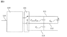
図3は、上述した補完方法を実行するのに用いられる回路の包括概略図である。インターフェース回路100は、少なくとも、接続されたコンデンサの容量値をアナログまたはデジタル出力信号110に変換するように構成された容量変換部を備える。出力信号110は、物理量の値を表す電気信号として特徴付けられてもよい。容量センサの場合、出力信号は、取得容量値に対応する、または、取得容量値を表すアナログまたはデジタル信号でもよい。切替部101は、全センサ容量CStot、または、全補完配線容量CCtotを容量変換部の入力端子に接続することを可能にする。多重化、つまり、2つの容量の切り替えは、それらの環境における誘電率の変化の速度に十分応じた頻度でなされるべきである。その頻度は、ある場合は10分間に1度かもしれないし、他の場合はミリ秒ごとかもしれない。
FIG. 3 is a general schematic diagram of the circuits used to implement the above-described complement method. The
この構成では、3タイプの配線が存在する。センサ配線111は、切替部101の一方の多重化入力端子と接合され、切替部101を介してセンサをインターフェース回路100の容量変換部に接続する。補完配線113は、切替部101の他方の多重化入力端子と接合される。共通配線112は、インターフェース回路100の容量変換部の入力端子と直接接合されることが好ましい。
In this configuration, there are three types of wiring. The
図3の回路の代わりに、別の回路を用いて図1および図2の機能を実装してもよい。 Instead of the circuit of FIG. 3, another circuit may be used to implement the functions of FIGS.
図4は、複合変換部と切替部とを備えた回路の実装例の概略図である。この実装は積分型コンバータからなり、定電流Iが電流源210から増幅器220の反転入力端子に供給され、積分ベース容量が反転入力端子(−)と増幅器220の出力端子との間に発生する。図4の回路において、出力端子110に出力される出力電圧は、積分ベース容量に比例する一定の傾きで上昇する。この傾きは、2つの閾値電圧レベル検出器とパルスカウンタとで測定してもよい(図示せず)。積分ベース容量は、ベース容量225と、スイッチ101の位置に応じた全センサ容量CStotまたは全補完配線容量CCtotとの和である。全補完配線容量CCtotの値は非常に小さくてもよく、出力電圧の傾きは、2つの出力電圧閾値レベル間の時間を非実際的な短時間にするかなりの急勾配でもよいため、ベース容量225が必要である。式(2)を適用する前に、ベース容量225の既知の値を、全センサ容量CStotおよび全補完配線容量CCtotから差し引く。これは、ベース容量225のみがコンバータに切り替わった、スイッチ101の第3位置を有することによって容易に実装される。
FIG. 4 is a schematic diagram of an implementation example of a circuit including a composite conversion unit and a switching unit. This implementation consists of an integrating converter, a constant current I is supplied from the
図5は、補完済センサ容量を算出する処理のフロー図である。 FIG. 5 is a flowchart of the process of calculating the supplemented sensor capacity.
フェーズ41において、切替回路を、ベース容量に向かう配線と接合するように変更し、ベース容量を測定する。このフェーズは、図4に示したようにベース容量を用いる場合にのみ必要である。測定すべきベース容量がなければ、フェーズ41は省略してもよい。フェーズ42において、切替回路を、センサ配線と接合するように変更し、全センサ容量を測定する。フェーズ43において、切替回路を、補完配線と接合するように変更し、全補完配線容量を測定する。フェーズ41においてベース容量を測定した場合は、まずベース容量値を全センサ配線容量値と全補完配線容量値の両方から差し引き、そして、算出フェーズ44において式(2)を用いて補完済センサ容量を算出する。ベース容量を測定しなかった場合は、測定した全センサ容量および全補完配線容量に基づいて、補完済センサ容量を直接算出してもよい。ステップ42、43、および、44は、第1連続ループとして繰り返してもよい。ベース容量が利用可能な場合は、代わりに、フェーズ41、42、43、および、44を通るループを選択することによって測定を定期的に校正してもよい。当業者には当然のことながら、フェーズ42および43は、発明の範囲を逸脱することなく、入れ替えてもよい。
In
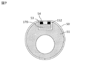
図5、6、および、7は、本発明の例示的な実施の形態1を示している。本実施の形態では、インターフェース回路100と容量センサ70とが、フレキシブル回路基板50にフリップチップ接合された半導体チップによって実装された医療用カテーテルデバイスの構造を開示している。当業者には当然のことながら、フリップチップ接合とは、半田バンプまたは他の同等突起部材が半導体チップのチップパッドに設けられた半導体ベアチップを、リフロー半田付けや導電性接着剤などによって外部回路に直接接合する半導体実装技術のことを指す。
5, 6, and 7 show an exemplary embodiment 1 of the present invention. In the present embodiment, the structure of the medical catheter device in which the
図5および6は、医療用カテーテルデバイスの断面図である。この断面では、容量センサチップ70かインターフェース回路100のどちらかを同じように表すことができる。フリップチップ型インターフェース回路100およびフリップチップ型容量センサ170は共に、半田バンプ53によって、フレキシブル回路基板50の面上に露出しているワイヤ54と接合される。フレキシブル回路基板50は、中空のカテーテル本体51の側壁内に生成された凹部52にインターフェース回路100および容量センサ170が共に配置されるように、医療用カテーテル本体51に巻き付けられる。
5 and 6 are cross-sectional views of medical catheter devices. In this cross section, either the
校正係数kを定義するために、図6で示した最初は空気で満たされている取付凹部52を、図7で図示するようにモールド材152で埋める。モールド材152は、例えば、シリコンゲルでもよい。取付凹部52は、回路およびその配線の周囲環境を表す。
To define the calibration factor k, the initially air-filled mounting
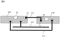
図8は、隣接するセンサチップ170の端とインターフェース回路チップ100の端との間の配線である。チップパッド70は、半田バンプ53によってフレキシブル回路基板上のワイヤと接合される。センサ170とインターフェース回路100とを互いに電気接続させる配線トラック111、112は、フレキシブル回路基板50上に配置される。補完配線トラック113は、インターフェース回路100の入力端子にのみ接続され、センサ170と配線回路100との間に配置されたセンサ配線トラック111を、センサ配線トラック111のすぐそばでできる限り近接して倣う。トラック配置の目的は、センサ配線トラック111と補完配線トラック113の両方から共通配線トラック112まで等しい容量を有することである。容量が等しければ、正確な重み係数kの取得が容易になる。
FIG. 8 shows wiring between the ends of the
図9、10、11、および、12は、本発明の例示的な実施の形態2を示している。実施の形態2は、特に、補完方法の妥当性を検証するのに有用である。 9, 10, 11, and 12 show an exemplary embodiment 2 of the present invention. The second embodiment is particularly useful for verifying the validity of the complement method.
図9は、実施の形態2に係る、インターフェース回路チップ100と、容量センサチップ170と、その配線との上面図である。ここで、チップパッド70は、ボンドワイヤで相互接続される。補完配線ボンドワイヤ113の配置を可能にするフローティングボンドパッド80を設ける。フローティングボンドパッドとは、ボンディングの機械的作用を可能にするパッドのことを指すが、電気接続を提供するものではない。センサ配線ボンドワイヤ111および共通配線ボンドワイヤ112に加えて、さらなるボンドワイヤを配置してもよい。この例では、グランド配線ボンドワイヤ114がある。補完配線ボンドワイヤ113は、補完配線ボンドワイヤ113と共通配線ボンドワイヤ112との間の容量が、センサ配線ボンドワイヤ111と共通配線ボンドワイヤ112との間の容量にできるだけ近づくように、配置される。
FIG. 9 is a top view of the
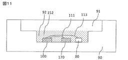
図10、11、および、12は、セラミック筺体90に回路を配置した実施の形態2の断面図である。セラミック筺体は、インターフェース回路100と、センサ170と、配線ボンドワイヤ111、112、113、114と、フローティングボンドパッド80とが配置される下部キャビティ92を有する。この断面図では、センサ配線ボンドワイヤ111と補完配線ボンドワイヤ113のみを示している。本実施の形態は、オプションの上部キャビティ91も有する。上部キャビティ91を用いて補完方法の有効性を試してもよいが、商品に必要なものではない。下部キャビティ92、または、下部キャビティ92と上部キャビティ91の組み合わせは、キャビティに配置された回路およびその配線の周囲環境を表す。
10, 11, and 12 are cross-sectional views of the second embodiment in which a circuit is arranged in the
図10において、ベアチップ100、170は、下部キャビティ92に配置され、ボンドワイヤ111、113で接合される。キャビティはそれ以外中身がなく、誘電率εr=1の空気で通常満たされている。様々な配線の容量を測定して、正確な圧力測定値に向けてセンサ170を校正してもよい。
In FIG. 10, the
図11は、下部キャビティ92がモールド材152で埋められた、実験の第2段階である。このモールド材は、例えば、誘電率が空気とは異なるシリコンゲルでもよい。ゲルモールドしたことによる容量変化を測定し、ここで、容量測定結果に基づいて重み係数kの値を算出してもよい。
FIG. 11 shows the second stage of the experiment in which the
行った実験において、算出された重み係数は、値k=0.835であった。予想どおり、重み係数値は1より小さい。なぜなら、補完配線ボンドワイヤ113は、センサ配線ボンドワイヤ111より長く、共通配線ボンドワイヤにより近いので、補完配線ボンドワイヤの配線容量が、センサ配線ボンドワイヤによるセンサ配線容量より大きくなるからである。
In the experiments carried out, the calculated weighting factor was the value k = 0.835. As expected, the weighting factor value is less than one. This is because the complementary
図12は、上部キャビティ91が食塩水溶液93で満たされた、実験の第3段階である。本実験は、実施の形態1のカテーテルを利用する模倣環境を意図したものであるが、体液をまねるために1%の食塩水溶液を用いた。しばらくしてから、配線間の容量を再度測定した。
FIG. 12 is the third stage of the experiment, where the
図13は、図9、10、および、11の実験段階の結果である。センサから受信した測定値における圧力誤差の結果を2組示す。実線で結ばれたひし形でマークされている1組目の結果は、補完なし、つまり、重み係数がk=0の場合の圧力誤差を示している。この組の結果を非補完結果と呼ぶ。点線で結ばれた四角でマークされている2組目の結果は、補完あり、つまり、取得した重み係数k=0.835を用いた圧力誤差を示している。この組の結果を補完結果と呼ぶ。 FIG. 13 is the result of the experimental stage of FIGS. 9, 10 and 11. Two sets of pressure error results in the measurements received from the sensors are shown. The result of the first set, which is marked by a diamond connected by a solid line, shows the pressure error when there is no complement, that is, when the weighting factor is k = 0. The result of this set is called the non-complementary result. The result of the second set, which is marked by a square connected by a dotted line, indicates complementation, that is, the pressure error using the obtained weighting coefficient k = 0.835. The result of this set is called the complement result.
図10で示された初期段階において、圧力誤差は、非補完結果と補完結果とで大きな差はない。モールド材152を塗布した後、配線容量の変化による非補完圧力誤差は2200Paになり、モールドした回路を食塩水にさらした後では、非補完圧力誤差は1500Paのレベルになるが、補完測定値では、充填材があるかどうか食塩水があるかどうかに関係なく、圧力誤差は基本的に同じままである。圧力誤差が減少した理由、そのために食塩水を加えたまま第3段階で容量を測定した理由は、モールド材の上にある電気伝導性を有する食塩水が、配線周りにシールドグランド電位を付加して配線容量を低減させたからである。図13における初期圧力誤差および全補完圧力誤差は、全て約+200Paである。独立校正係数が3つの1次双曲線関数である選択校正関数Pを用いて大気圧周辺で取得されるこの誤差は、最小である。
In the initial stage shown in FIG. 10, the pressure error does not significantly differ between the non-complementary result and the complementary result. After applying the
図9〜13に示された実験により、発明した補完方法の有効性が証明された。 The experiments shown in FIGS. 9 to 13 proved the effectiveness of the invented complementation method.
技術が進歩するにつれて本発明の基本概念を様々な方法で実装できることは、当業者にとって自明である。したがって、本発明およびその実施の形態は、上記の例に限定されず、請求項の範囲内で異なっていてもよい。 It will be obvious to a person skilled in the art that as the technology advances, the basic idea of the invention can be implemented in various ways. Therefore, the invention and its embodiments are not limited to the examples described above, but may vary within the scope of the claims.
Claims (13)
前記センサ配線から全センサ容量値を取得し、
前記補完配線から全補完配線容量値を取得し、
取得した前記全センサ容量値から、取得した前記全補完配線容量値であって、重み係数をかけあわせた前記全補完配線容量値を差し引くことによって、補完済センサ容量値を算出し、
前記インターフェース回路の出力端子において前記補完済センサ容量値に対応する電気信号を出力し、
前記補完配線は、前記インターフェース回路にのみ電気接続され、
前記重み係数を、
第1測定において、第1全センサ容量値と第1全補完配線容量値とを測定するステップと、
前記容量センサと前記容量センサの配線とを、空気より大きい誘電率を有するモールド材で覆うことによるそれらの周囲環境における比誘電率の変化にさらすステップと、
前記容量センサと前記容量センサの配線とを、前記モールド材に起因するそれらの周囲環境における前記比誘電率の変化にさらした後、第2測定において、第2全センサ容量値と第2全補完配線容量値とを測定するステップと、
前記第1全センサ容量値と前記第2全センサ容量値との間の変化に基づいて、測定した全センサ容量の変化を算出し、前記第1全補完配線容量値と前記第2全補完配線容量値との間の変化に基づいて、測定した全補完配線容量の変化を算出するステップと、
前記測定した全センサ容量の変化を前記測定した全補完配線容量の変化で割ることにより前記重み係数を算出するステップとによって取得することにより、
前記重み係数を用いて算出された前記補完済センサ容量値は、前記容量センサと前記インターフェース回路とその配線との周囲環境における比誘電率の変化に依存しない
方法。 A method of canceling the influence of a change in wiring capacitance on a capacitance sensor measurement value output by a capacitance sensor connected to an interface circuit having at least two wirings including a sensor wiring and a complementary wiring arranged in the immediate vicinity of the sensor wiring. There
Obtain all sensor capacitance values from the sensor wiring,
Obtaining all complementary wiring capacitance values from the complementary wiring,
From the obtained total sensor capacitance value, the obtained total complementary wiring capacitance value, by subtracting the total complementary wiring capacitance value multiplied by a weighting factor, to calculate the complementary sensor capacitance value,
An electric signal corresponding to the complemented sensor capacitance value is output at the output terminal of the interface circuit,
The complementary wiring is electrically connected only to the interface circuit,
The weighting factor is
Measuring the first total sensor capacitance value and the first total complementary wiring capacitance value in the first measurement;
Exposing the capacitance sensor and the wiring of the capacitance sensor to changes in the relative permittivity in their ambient environment by covering with a molding material having a permittivity greater than air;
After exposing the capacitance sensor and the wiring of the capacitance sensor to the change in the relative dielectric constant in the ambient environment caused by the molding material, in the second measurement, the second total sensor capacitance value and the second total complement. Measuring the wiring capacitance value and
A change in the measured total sensor capacitance is calculated based on a change between the first total sensor capacitance value and the second total sensor capacitance value, and the first total complementary wiring capacitance value and the second total complementary wiring capacitance are calculated. Calculating a change in the measured total complementary wiring capacitance based on the change between the capacitance value and
By calculating the weighting factor by dividing the change in the measured total sensor capacitance by the change in the measured total complementary wiring capacitance,
The complementary sensor capacitance value calculated using the weighting factor does not depend on a change in relative permittivity in the surrounding environment of the capacitance sensor, the interface circuit and its wiring.
前記インターフェース回路の第1入力端子において前記センサ配線が接合され、前記インターフェース回路の第2入力端子において共通配線が接合される場合、前記インターフェース回路によって前記全センサ容量値を取得し、
前記インターフェース回路の第1入力端子において前記補完配線が接合され、前記インターフェース回路の第2入力端子において前記共通配線が接合される場合、前記インターフェース回路によって前記全補完配線容量値を取得する
請求項1に記載の方法。 further,
When the sensor wiring is joined at the first input terminal of the interface circuit and the common wiring is joined at the second input terminal of the interface circuit, the total capacitance value of the sensor is acquired by the interface circuit,
The total complementary wiring capacitance value is acquired by the interface circuit when the complementary wiring is joined at a first input terminal of the interface circuit and the common wiring is joined at a second input terminal of the interface circuit. The method described in.
前記全センサ容量値を取得するための前記センサ配線と、前記全補完配線容量値を取得するための前記補完配線とのうちのいずれか一つに接続されるように前記インターフェース回路の第1入力端子を多重化し、
前記多重化は、10ミリ秒から10分の範囲における頻度で発生する
請求項2に記載の方法。 further,
The first input of the interface circuit is connected to one of the sensor wiring for obtaining the total sensor capacitance value and the complementary wiring for obtaining the total complementary wiring capacitance value. Multiplex the terminals,
The method of claim 2, wherein the multiplexing occurs with a frequency in the range of 10 milliseconds to 10 minutes.
前記インターフェース回路の第1入力端子において積分ベース容量のみが接合され、前記インターフェース回路の第2入力端子において共通配線が接合される場合、前記インターフェース回路によって積分ベース容量値を取得し、
前記インターフェース回路の第1入力端子において前記センサ配線が接合され、前記インターフェース回路の第2入力端子において前記共通配線が接合される場合、前記インターフェース回路によって、前記積分ベース容量値を含む前記全センサ容量値を取得し、
前記インターフェース回路の第1入力端子において前記補完配線が接合され、前記インターフェース回路の第2入力端子において前記共通配線が接合される場合、前記インターフェース回路によって、前記積分ベース容量値を含む前記全補完配線容量値を取得し、
前記補完済センサ容量値を算出する前に、前記積分ベース容量値を前記全センサ容量値と前記全補完配線容量値の両方から差し引く
請求項1に記載の方法。 further,
When only the integral base capacitance is joined at the first input terminal of the interface circuit and the common wiring is joined at the second input terminal of the interface circuit, the integral base capacitance value is acquired by the interface circuit,
When the sensor wiring is joined at the first input terminal of the interface circuit and the common wiring is joined at the second input terminal of the interface circuit, the total sensor capacitance including the integrated base capacitance value is generated by the interface circuit. Get the value,
When the complementary wiring is joined at the first input terminal of the interface circuit and the common wiring is joined at the second input terminal of the interface circuit, the entire complementary wiring including the integrated base capacitance value is provided by the interface circuit. Get the capacity value,
The method of claim 1, wherein the integrated base capacitance value is subtracted from both the total sensor capacitance value and the total complementary wiring capacitance value before calculating the supplemented sensor capacitance value.
前記全センサ容量値を取得するための前記センサ配線と、前記全補完配線容量値を取得するための前記補完配線と、前記積分ベース容量値を取得するための前記積分ベース容量とのうちのいずれか一つに接続されるように前記インターフェース回路の第1入力端子を多重化し、
前記多重化は、10ミリ秒から10分の範囲における頻度で発生する
請求項4に記載の方法。 further,
Any of the sensor wiring for obtaining the total sensor capacitance value, the complementary wiring for obtaining the total complementary wiring capacitance value, and the integral base capacitance for obtaining the integral base capacitance value Multiplex the first input terminal of the interface circuit so that it is connected to one
The method of claim 4, wherein the multiplexing occurs with a frequency in the range of 10 milliseconds to 10 minutes.
前記補完配線と前記共通配線との間の容量が前記センサ配線と前記共通配線との間の容量と実質的に等しくなるように、前記補完配線を配置する
請求項2から5のいずれか1項に記載の方法。 further,
The complementary wiring is arranged so that the capacitance between the complementary wiring and the common wiring is substantially equal to the capacitance between the sensor wiring and the common wiring.
The method according to any one of 5 請 Motomeko 2.
校正関数を定義するステップと、
第1全センサ容量値と、第1全補完容量値と、第1基準圧力値とを測定するステップと、
ダミー重み係数を用いて、前記第1全センサ容量値と前記第1全補完容量値とに基づいて、第1補完済センサ容量値を算出するステップと、
前記校正関数を用いて、前記第1補完済センサ容量値に対応する第1圧力値を算出する
ステップと、
前記容量センサと前記容量センサの配線とを、それらの周囲環境における比誘電率の変化にさらすステップと、
前記容量センサと前記容量センサの配線とをそれらの周囲環境における前記比誘電率の変化にさらした後、第2全センサ容量値と、第2全補完容量値と、第2基準圧力値とを測定するステップと、
前記第2全センサ容量値と前記第2全補完容量値とに基づいて、第2補完済センサ容量値を算出するステップと、
前記校正関数を用いて、前記第2補完済センサ容量値に基づいて第2圧力値を算出するステップと、
調節後の前記重み係数を用いて算出される第1圧力誤差が、同じ調節後の前記重み係数を用いて算出される第2圧力誤差と等しくなるように、前記第1補完済センサ容量値と前記第2補完済センサ容量値と前記第1圧力値と前記第2圧力値とを算出するのに用いられる前記重み係数を調節することにより前記重み係数を取得するステップとによって取得し、前記第1圧力誤差は、調節後の前記重み係数を用いて算出される前記第1圧力値と前記第1基準圧力値との差に等しく、前記第2圧力誤差は、調節後の前記重み係数を用いて算出される前記第2圧力値と前記第2基準圧力値との差に等しい
請求項1から6のいずれか1項に記載の方法。 The weighting factor is
Defining a calibration function,
Measuring a first total sensor capacitance value, a first total complementary capacitance value, and a first reference pressure value,
Calculating a first complemented sensor capacitance value based on the first total sensor capacitance value and the first total complementary capacitance value using a dummy weighting factor;
Calculating a first pressure value corresponding to the first complemented sensor capacitance value using the calibration function;
Exposing the capacitance sensor and the wiring of the capacitance sensor to changes in the relative permittivity in their ambient environment;
After exposing the capacitance sensor and the wiring of the capacitance sensor to the change in the relative dielectric constant in their surrounding environment, the second total sensor capacitance value, the second total complementary capacitance value, and the second reference pressure value are Measuring step,
Calculating a second supplemented sensor capacitance value based on the second total sensor capacitance value and the second total supplemental capacitance value;
Calculating a second pressure value based on the second complemented sensor capacitance value using the calibration function;
With the first supplemented sensor capacitance value, the first pressure error calculated using the adjusted weighting coefficient is equal to the second pressure error calculated using the same adjusted weighting coefficient. Acquiring the weighting factor by adjusting the weighting factor used to calculate the second complemented sensor capacitance value, the first pressure value, and the second pressure value. 1 pressure error is equal to the difference between the first pressure value and the first reference pressure value calculated using the adjusted weighting factor, and the second pressure error uses the adjusted weighting factor. 7. The method according to any one of claims 1 to 6, which is equal to a difference between the second calculated pressure value and the second reference pressure value.
前記センサ配線から前記容量センサの全センサ容量値を取得し、
前記補完配線から全補完配線容量値を取得し、
取得した前記全センサ容量値から、重み係数をかけ合わせた取得した前記全補完配線容量値を差し引くことによって、補完済センサ容量値を算出し、
前記インターフェース回路の出力端子において前記補完済センサ容量値に対応する電気信号を出力するように構成され、
前記補完配線は、前記インターフェース回路にのみ電気接続され、
前記容量センサと前記インターフェース回路とそれらの配線とは、空気より大きい誘電率を有するモールド材で覆われ、前記重み係数を、前記モールド材をつける前と後とに行われる容量値測定に基づいて定義するように構成することにより、
前記重み係数を用いて算出された前記補完済センサ容量値は、前記容量センサと前記インターフェース回路とその配線との周囲環境における比誘電率の変化に依存しない
装置。 A capacitance sensor and an interface circuit are provided, and the capacitance sensor is connected to the interface circuit having at least two wirings including a sensor wiring and a complementary wiring arranged in the immediate vicinity of the sensor wiring. A device configured to cancel the influence of the change in wiring capacitance of
Obtaining the total sensor capacitance value of the capacitance sensor from the sensor wiring,
Obtaining all complementary wiring capacitance values from the complementary wiring,
From the obtained total sensor capacitance value, by subtracting the obtained all complementary wiring capacitance value multiplied by a weighting factor, to calculate the complementary sensor capacitance value,
The output terminal of the interface circuit is configured to output an electrical signal corresponding to the complemented sensor capacitance value,
The complementary wiring is electrically connected only to the interface circuit,
The capacitance sensor, the interface circuit, and their wiring are covered with a molding material having a dielectric constant larger than that of air, and the weighting factor is determined based on capacitance value measurement performed before and after the molding material is attached. By configuring to define,
The complemented sensor capacitance value calculated using the weighting factor does not depend on a change in relative permittivity in a surrounding environment of the capacitance sensor, the interface circuit, and its wiring.
前記全センサ容量値を取得するための前記センサ配線と、
前記全補完配線容量値を取得するための前記補完配線とのうちの
いずれか一つに接続されるように前記インターフェース回路の第1入力端子を多重化するよう構成されたスイッチを備え、
前記多重化は、10ミリ秒から10分の範囲における頻度で発生する
請求項8に記載の装置。 Common wiring is joined at the second input terminal of the interface circuit,
The sensor wiring for obtaining the total sensor capacitance value,
A switch configured to multiplex a first input terminal of the interface circuit so as to be connected to any one of the complementary wirings for obtaining the total complementary wiring capacitance value,
The apparatus of claim 8, wherein the multiplexing occurs with a frequency in the range of 10 milliseconds to 10 minutes.
積分ベース容量値を取得するための積分ベース容量のみと、
前記積分ベース容量値を含む前記全センサ容量値を取得するための前記センサ配線と、
前記積分ベース容量値を含む前記全補完配線容量値を取得するための前記補完配線とのうちの
いずれか一つに接続されるように前記インターフェース回路の第1入力端子を多重化するよう構成されたスイッチを備え、
前記多重化は、10ミリ秒から10分の範囲における頻度で発生し、さらに、前記補完済センサ容量値を算出する前に、前記積分ベース容量値を前記全センサ容量値と前記全補完配線容量値の両方から差し引くように構成された
請求項8に記載の装置。 Common wiring is joined at the second input terminal of the interface circuit,
Only the integration base capacity to get the integration base capacity value,
The sensor wiring for obtaining the total sensor capacitance value including the integrated base capacitance value,
It is configured to multiplex the first input terminal of the interface circuit so as to be connected to any one of the complementary wiring for obtaining the total complementary wiring capacitance value including the integrated base capacitance value. Equipped with a switch
The multiplexing occurs with a frequency in the range of 10 milliseconds to 10 minutes, and further, the integrated base capacitance value is set to the total sensor capacitance value and the total complementary wiring capacitance before calculating the supplemented sensor capacitance value. 9. The device of claim 8 configured to subtract from both values.
請求項9又は10に記載の装置。 The device according to claim 9 or 10, wherein the complementary wiring is arranged such that the capacitance between the complementary wiring and the common wiring is substantially equal to the capacitance between the sensor wiring and the common wiring. .
第1測定において、第1全センサ容量値と第1全補完配線容量値とを測定し、
前記容量センサと前記容量センサの配線とをそれらの周囲環境における比誘電率の変化にさらした後、第2測定において、第2全センサ容量値と第2全補完配線容量値とを測定し、
前記第1全センサ容量値と前記第2全センサ容量値との間の変化に基づいて、測定した全センサ容量の変化を算出し、前記第1全補完配線容量値と前記第2全補完配線容量値との間の変化に基づいて、測定した全補完配線容量の変化を算出し、
前記測定した全センサ容量の変化を前記測定した全補完配線容量の変化で割ることにより前記重み係数を算出するように構成された
請求項9から11のいずれか1項に記載の装置。 further,
In the first measurement, the first total sensor capacitance value and the first total complementary wiring capacitance value are measured,
After exposing the capacitance sensor and the wiring of the capacitance sensor to changes in the relative dielectric constant in their surrounding environment, in the second measurement, the second total sensor capacitance value and the second total complementary wiring capacitance value are measured,
A change in the measured total sensor capacitance is calculated based on the change between the first total sensor capacitance value and the second total sensor capacitance value, and the first total complementary wiring capacitance value and the second total complementary wiring capacitance are calculated. Calculate the change in the measured total complementary wiring capacitance based on the change between the capacitance value and
12. The apparatus according to any one of claims 9 to 11, configured to calculate the weighting factor by dividing the measured change in total sensor capacitance by the measured change in total complementary wiring capacitance.
校正関数を定義し、
第1全センサ容量値と、第1全補完容量値と、第1基準圧力値とを測定し、
ダミー重み係数を用いて、前記第1全センサ容量値と前記第1全補完容量値とに基づいて、第1補完済センサ容量値を算出し、
前記校正関数を用いて、前記第1補完済センサ容量値に対応する第1圧力値を算出し、
前記容量センサと前記容量センサの配線とをそれらの周囲環境における比誘電率の変化にさらした後、第2全センサ容量値と、第2全補完容量値と、第2基準圧力値とを測定し、
前記第2全センサ容量値と前記第2全補完容量値とに基づいて、第2補完済センサ容量値を算出し、
前記校正関数を用いて、前記第2補完済センサ容量値に基づいて第2圧力値を算出し、
調節後の前記重み係数を用いて算出される第1圧力誤差が、同じ調節後の前記重み係数を用いて算出される第2圧力誤差と等しくなるように、前記第1補完済センサ容量値と前記第2補完済センサ容量値と前記第1圧力値と前記第2圧力値とを算出するのに用いられる前記重み係数を調節することにより前記重み係数を取得するように構成され、前記第1圧力誤差は、調節後の前記重み係数を用いて算出される前記第1圧力値と前記第1基準圧力値との差に等しく、前記第2圧力誤差は、調節後の前記重み係数を用いて算出される前記第2圧力値と前記第2基準圧力値との差に等しい
請求項9から12のいずれか1項に記載の装置。 further,
Define a calibration function,
Measuring a first total sensor capacitance value, a first total complementary capacitance value, and a first reference pressure value,
Calculating a first supplemented sensor capacitance value based on the first total sensor capacitance value and the first total supplemental capacitance value using a dummy weighting factor;
Calculating a first pressure value corresponding to the first supplemented sensor capacitance value using the calibration function,
The second total sensor capacitance value, the second total complementary capacitance value, and the second reference pressure value are measured after exposing the capacitance sensor and the wiring of the capacitance sensor to changes in the relative permittivity in their surrounding environment. Then
Calculating a second complemented sensor capacitance value based on the second total sensor capacitance value and the second total complementary capacitance value,
Calculating a second pressure value based on the second complemented sensor capacitance value using the calibration function,
With the first supplemented sensor capacitance value, the first pressure error calculated using the adjusted weighting coefficient is equal to the second pressure error calculated using the same adjusted weighting coefficient. The weighting factor is configured to be obtained by adjusting the weighting factor used to calculate the second complemented sensor capacitance value, the first pressure value, and the second pressure value. The pressure error is equal to the difference between the first pressure value and the first reference pressure value calculated using the adjusted weighting factor, and the second pressure error is calculated using the adjusted weighting factor. 13. The device according to any one of claims 9 to 12, which is equal to a difference between the calculated second pressure value and the second reference pressure value.
Applications Claiming Priority (2)
| Application Number | Priority Date | Filing Date | Title |
|---|---|---|---|
| FI20176012 | 2017-11-13 | ||
| FI20176012 | 2017-11-13 |
Publications (2)
| Publication Number | Publication Date |
|---|---|
| JP2019105626A JP2019105626A (en) | 2019-06-27 |
| JP6696552B2 true JP6696552B2 (en) | 2020-05-20 |
Family
ID=64267580
Family Applications (1)
| Application Number | Title | Priority Date | Filing Date |
|---|---|---|---|
| JP2018206982A Active JP6696552B2 (en) | 2017-11-13 | 2018-11-02 | Wiring capacity canceling method and wiring capacity canceling device |
Country Status (3)
| Country | Link |
|---|---|
| US (1) | US11248977B2 (en) |
| EP (1) | EP3483564B1 (en) |
| JP (1) | JP6696552B2 (en) |
Family Cites Families (12)
| Publication number | Priority date | Publication date | Assignee | Title |
|---|---|---|---|---|
| BE551788A (en) | 1955-10-19 | |||
| GB2071852A (en) | 1980-03-12 | 1981-09-23 | Rolls Royce | Capacitance frequency modulation probe for blade tip clearance measurement |
| US5431057A (en) * | 1990-02-12 | 1995-07-11 | Fraunhofer-Gesellschaft Zur Forderung Der Angewandten Forschung E.V. | Integratable capacitative pressure sensor |
| DE4004179A1 (en) * | 1990-02-12 | 1991-08-14 | Fraunhofer Ges Forschung | INTEGRATABLE, CAPACITIVE PRESSURE SENSOR AND METHOD FOR PRODUCING THE SAME |
| JP3567089B2 (en) * | 1998-10-12 | 2004-09-15 | 株式会社日立製作所 | Capacitive pressure sensor |
| JP2009257916A (en) * | 2008-04-16 | 2009-11-05 | Oki Semiconductor Co Ltd | Capacitive pressure sensor and method of providing capacitance compensation signal |
| JP2013024808A (en) * | 2011-07-25 | 2013-02-04 | Japan Aerospace Exploration Agency | Measuring apparatus and measuring method |
| US20140026642A1 (en) * | 2012-07-25 | 2014-01-30 | John O. O'Connell | Capacitive sensor comprising differing unit cell structures |
| FI125447B (en) | 2013-06-04 | 2015-10-15 | Murata Manufacturing Co | Improved pressure gauge structure |
| US9285404B2 (en) * | 2013-08-15 | 2016-03-15 | Freescale Semiconductor, Inc. | Test structure and methodology for estimating sensitivity of pressure sensors |
| EP2988122B1 (en) | 2014-08-20 | 2019-04-24 | ams international AG | Capacitive sensor |
| CN106403922A (en) | 2015-07-31 | 2017-02-15 | 立锜科技股份有限公司 | Micro-electromechanical element with electric compensation and reading circuit thereof |
-
2018
- 2018-11-02 JP JP2018206982A patent/JP6696552B2/en active Active
- 2018-11-07 EP EP18204798.5A patent/EP3483564B1/en active Active
- 2018-11-12 US US16/186,966 patent/US11248977B2/en active Active
Also Published As
| Publication number | Publication date |
|---|---|
| JP2019105626A (en) | 2019-06-27 |
| EP3483564A1 (en) | 2019-05-15 |
| US20190145843A1 (en) | 2019-05-16 |
| US11248977B2 (en) | 2022-02-15 |
| EP3483564B1 (en) | 2021-07-14 |
Similar Documents
| Publication | Publication Date | Title |
|---|---|---|
| US11768122B2 (en) | Liquid detection in a sensor environment and remedial action thereof | |
| US10398343B2 (en) | Perspiration sensor | |
| CN106298746B (en) | Vertical Magnetic Barriers for Integrated Electronic Modules | |
| US8330236B2 (en) | Isolation channel improving measurement accuracy of MEMS devices | |
| US9709446B2 (en) | Module for integration into a mobile terminal to measure the ambient temperature | |
| RU2015116636A (en) | DOSING DEVICE FOR THE INTRODUCTION OF MEDICINES | |
| CN106053915A (en) | Current sensor | |
| US7019540B2 (en) | Electrostatic capacitance detection circuit and microphone device | |
| JP6533536B2 (en) | Compensation of target object binding to feed lines in capacitive sensing systems | |
| US7005865B2 (en) | Circuit and method for impedance detection | |
| US7034551B2 (en) | Electrostatic capacitance detection circuit and microphone device | |
| JP6696552B2 (en) | Wiring capacity canceling method and wiring capacity canceling device | |
| TWI466599B (en) | Circuit board and method for testing component built in the circuit board | |
| EP3372969A1 (en) | Temperature measurement integrated circuit with flexible cable and sensing element | |
| KR101559154B1 (en) | Pressure sensor package and manufacturing method thereof | |
| JP6522740B2 (en) | Load measuring device | |
| US20260036441A1 (en) | In-situ capacitance detection for integrated circuits and mems sensors | |
| US10690706B2 (en) | Device for measuring an electrical quantity of one phase of an AC electric current of an overhead electrical network | |
| WO2006113325A2 (en) | Integrated tilt sensor | |
| CN109416291A (en) | Pressure difference transducer | |
| Dogan et al. | Miniaturized Multi Sensor Implant for Monitoring of Hemodynamic Parameters | |
| CN121323753A (en) | Trimmable fluid level sensor strip | |
| CN121740968A (en) | Packaged MEMS devices with humidity sensors | |
| Belavic et al. | Thick Film Interconnections for Sensor Applications | |
| TH124034A (en) | Infrared sensor |
Legal Events
| Date | Code | Title | Description |
|---|---|---|---|
| A621 | Written request for application examination |
Free format text: JAPANESE INTERMEDIATE CODE: A621 Effective date: 20190304 |
|
| A131 | Notification of reasons for refusal |
Free format text: JAPANESE INTERMEDIATE CODE: A131 Effective date: 20191210 |
|
| A977 | Report on retrieval |
Free format text: JAPANESE INTERMEDIATE CODE: A971007 Effective date: 20191211 |
|
| A601 | Written request for extension of time |
Free format text: JAPANESE INTERMEDIATE CODE: A601 Effective date: 20200207 |
|
| A521 | Request for written amendment filed |
Free format text: JAPANESE INTERMEDIATE CODE: A523 Effective date: 20200217 |
|
| A131 | Notification of reasons for refusal |
Free format text: JAPANESE INTERMEDIATE CODE: A131 Effective date: 20200303 |
|
| A521 | Request for written amendment filed |
Free format text: JAPANESE INTERMEDIATE CODE: A523 Effective date: 20200309 |
|
| TRDD | Decision of grant or rejection written | ||
| A01 | Written decision to grant a patent or to grant a registration (utility model) |
Free format text: JAPANESE INTERMEDIATE CODE: A01 Effective date: 20200324 |
|
| A61 | First payment of annual fees (during grant procedure) |
Free format text: JAPANESE INTERMEDIATE CODE: A61 Effective date: 20200406 |
|
| R150 | Certificate of patent or registration of utility model |
Ref document number: 6696552 Country of ref document: JP Free format text: JAPANESE INTERMEDIATE CODE: R150 |