JP6689691B2 - Wiring board and manufacturing method thereof - Google Patents
Wiring board and manufacturing method thereof Download PDFInfo
- Publication number
- JP6689691B2 JP6689691B2 JP2016137740A JP2016137740A JP6689691B2 JP 6689691 B2 JP6689691 B2 JP 6689691B2 JP 2016137740 A JP2016137740 A JP 2016137740A JP 2016137740 A JP2016137740 A JP 2016137740A JP 6689691 B2 JP6689691 B2 JP 6689691B2
- Authority
- JP
- Japan
- Prior art keywords
- layer
- wiring
- wiring board
- insulating layer
- pad
- Prior art date
- Legal status (The legal status is an assumption and is not a legal conclusion. Google has not performed a legal analysis and makes no representation as to the accuracy of the status listed.)
- Active
Links
Images


Classifications
-
- H—ELECTRICITY
- H01—ELECTRIC ELEMENTS
- H01L—SEMICONDUCTOR DEVICES NOT COVERED BY CLASS H10
- H01L23/00—Details of semiconductor or other solid state devices
- H01L23/48—Arrangements for conducting electric current to or from the solid state body in operation, e.g. leads, terminal arrangements ; Selection of materials therefor
- H01L23/488—Arrangements for conducting electric current to or from the solid state body in operation, e.g. leads, terminal arrangements ; Selection of materials therefor consisting of soldered or bonded constructions
- H01L23/498—Leads, i.e. metallisations or lead-frames on insulating substrates, e.g. chip carriers
- H01L23/49827—Via connections through the substrates, e.g. pins going through the substrate, coaxial cables
-
- H—ELECTRICITY
- H01—ELECTRIC ELEMENTS
- H01L—SEMICONDUCTOR DEVICES NOT COVERED BY CLASS H10
- H01L21/00—Processes or apparatus adapted for the manufacture or treatment of semiconductor or solid state devices or of parts thereof
- H01L21/67—Apparatus specially adapted for handling semiconductor or electric solid state devices during manufacture or treatment thereof; Apparatus specially adapted for handling wafers during manufacture or treatment of semiconductor or electric solid state devices or components ; Apparatus not specifically provided for elsewhere
- H01L21/683—Apparatus specially adapted for handling semiconductor or electric solid state devices during manufacture or treatment thereof; Apparatus specially adapted for handling wafers during manufacture or treatment of semiconductor or electric solid state devices or components ; Apparatus not specifically provided for elsewhere for supporting or gripping
- H01L21/6835—Apparatus specially adapted for handling semiconductor or electric solid state devices during manufacture or treatment thereof; Apparatus specially adapted for handling wafers during manufacture or treatment of semiconductor or electric solid state devices or components ; Apparatus not specifically provided for elsewhere for supporting or gripping using temporarily an auxiliary support
-
- H—ELECTRICITY
- H01—ELECTRIC ELEMENTS
- H01L—SEMICONDUCTOR DEVICES NOT COVERED BY CLASS H10
- H01L23/00—Details of semiconductor or other solid state devices
- H01L23/12—Mountings, e.g. non-detachable insulating substrates
- H01L23/13—Mountings, e.g. non-detachable insulating substrates characterised by the shape
-
- H—ELECTRICITY
- H01—ELECTRIC ELEMENTS
- H01L—SEMICONDUCTOR DEVICES NOT COVERED BY CLASS H10
- H01L23/00—Details of semiconductor or other solid state devices
- H01L23/48—Arrangements for conducting electric current to or from the solid state body in operation, e.g. leads, terminal arrangements ; Selection of materials therefor
- H01L23/488—Arrangements for conducting electric current to or from the solid state body in operation, e.g. leads, terminal arrangements ; Selection of materials therefor consisting of soldered or bonded constructions
- H01L23/498—Leads, i.e. metallisations or lead-frames on insulating substrates, e.g. chip carriers
-
- H—ELECTRICITY
- H01—ELECTRIC ELEMENTS
- H01L—SEMICONDUCTOR DEVICES NOT COVERED BY CLASS H10
- H01L24/00—Arrangements for connecting or disconnecting semiconductor or solid-state bodies; Methods or apparatus related thereto
- H01L24/80—Methods for connecting semiconductor or other solid state bodies using means for bonding being attached to, or being formed on, the surface to be connected
- H01L24/81—Methods for connecting semiconductor or other solid state bodies using means for bonding being attached to, or being formed on, the surface to be connected using a bump connector
-
- H—ELECTRICITY
- H01—ELECTRIC ELEMENTS
- H01L—SEMICONDUCTOR DEVICES NOT COVERED BY CLASS H10
- H01L24/00—Arrangements for connecting or disconnecting semiconductor or solid-state bodies; Methods or apparatus related thereto
- H01L24/91—Methods for connecting semiconductor or solid state bodies including different methods provided for in two or more of groups H01L24/80 - H01L24/90
- H01L24/92—Specific sequence of method steps
-
- H—ELECTRICITY
- H01—ELECTRIC ELEMENTS
- H01L—SEMICONDUCTOR DEVICES NOT COVERED BY CLASS H10
- H01L24/00—Arrangements for connecting or disconnecting semiconductor or solid-state bodies; Methods or apparatus related thereto
- H01L24/93—Batch processes
- H01L24/95—Batch processes at chip-level, i.e. with connecting carried out on a plurality of singulated devices, i.e. on diced chips
- H01L24/97—Batch processes at chip-level, i.e. with connecting carried out on a plurality of singulated devices, i.e. on diced chips the devices being connected to a common substrate, e.g. interposer, said common substrate being separable into individual assemblies after connecting
-
- H—ELECTRICITY
- H01—ELECTRIC ELEMENTS
- H01L—SEMICONDUCTOR DEVICES NOT COVERED BY CLASS H10
- H01L25/00—Assemblies consisting of a plurality of individual semiconductor or other solid state devices ; Multistep manufacturing processes thereof
- H01L25/03—Assemblies consisting of a plurality of individual semiconductor or other solid state devices ; Multistep manufacturing processes thereof all the devices being of a type provided for in the same subgroup of groups H01L27/00 - H01L33/00, or in a single subclass of H10K, H10N, e.g. assemblies of rectifier diodes
- H01L25/10—Assemblies consisting of a plurality of individual semiconductor or other solid state devices ; Multistep manufacturing processes thereof all the devices being of a type provided for in the same subgroup of groups H01L27/00 - H01L33/00, or in a single subclass of H10K, H10N, e.g. assemblies of rectifier diodes the devices having separate containers
- H01L25/105—Assemblies consisting of a plurality of individual semiconductor or other solid state devices ; Multistep manufacturing processes thereof all the devices being of a type provided for in the same subgroup of groups H01L27/00 - H01L33/00, or in a single subclass of H10K, H10N, e.g. assemblies of rectifier diodes the devices having separate containers the devices being of a type provided for in group H01L27/00
-
- H—ELECTRICITY
- H05—ELECTRIC TECHNIQUES NOT OTHERWISE PROVIDED FOR
- H05K—PRINTED CIRCUITS; CASINGS OR CONSTRUCTIONAL DETAILS OF ELECTRIC APPARATUS; MANUFACTURE OF ASSEMBLAGES OF ELECTRICAL COMPONENTS
- H05K1/00—Printed circuits
- H05K1/02—Details
- H05K1/11—Printed elements for providing electric connections to or between printed circuits
- H05K1/111—Pads for surface mounting, e.g. lay-out
- H05K1/112—Pads for surface mounting, e.g. lay-out directly combined with via connections
-
- H—ELECTRICITY
- H05—ELECTRIC TECHNIQUES NOT OTHERWISE PROVIDED FOR
- H05K—PRINTED CIRCUITS; CASINGS OR CONSTRUCTIONAL DETAILS OF ELECTRIC APPARATUS; MANUFACTURE OF ASSEMBLAGES OF ELECTRICAL COMPONENTS
- H05K1/00—Printed circuits
- H05K1/02—Details
- H05K1/11—Printed elements for providing electric connections to or between printed circuits
- H05K1/115—Via connections; Lands around holes or via connections
- H05K1/116—Lands, clearance holes or other lay-out details concerning the surrounding of a via
-
- H—ELECTRICITY
- H05—ELECTRIC TECHNIQUES NOT OTHERWISE PROVIDED FOR
- H05K—PRINTED CIRCUITS; CASINGS OR CONSTRUCTIONAL DETAILS OF ELECTRIC APPARATUS; MANUFACTURE OF ASSEMBLAGES OF ELECTRICAL COMPONENTS
- H05K3/00—Apparatus or processes for manufacturing printed circuits
- H05K3/007—Manufacture or processing of a substrate for a printed circuit board supported by a temporary or sacrificial carrier
-
- H—ELECTRICITY
- H05—ELECTRIC TECHNIQUES NOT OTHERWISE PROVIDED FOR
- H05K—PRINTED CIRCUITS; CASINGS OR CONSTRUCTIONAL DETAILS OF ELECTRIC APPARATUS; MANUFACTURE OF ASSEMBLAGES OF ELECTRICAL COMPONENTS
- H05K3/00—Apparatus or processes for manufacturing printed circuits
- H05K3/46—Manufacturing multilayer circuits
- H05K3/4611—Manufacturing multilayer circuits by laminating two or more circuit boards
- H05K3/4614—Manufacturing multilayer circuits by laminating two or more circuit boards the electrical connections between the circuit boards being made during lamination
- H05K3/4617—Manufacturing multilayer circuits by laminating two or more circuit boards the electrical connections between the circuit boards being made during lamination characterized by laminating only or mainly similar single-sided circuit boards
-
- H—ELECTRICITY
- H01—ELECTRIC ELEMENTS
- H01L—SEMICONDUCTOR DEVICES NOT COVERED BY CLASS H10
- H01L2221/00—Processes or apparatus adapted for the manufacture or treatment of semiconductor or solid state devices or of parts thereof covered by H01L21/00
- H01L2221/67—Apparatus for handling semiconductor or electric solid state devices during manufacture or treatment thereof; Apparatus for handling wafers during manufacture or treatment of semiconductor or electric solid state devices or components; Apparatus not specifically provided for elsewhere
- H01L2221/683—Apparatus for handling semiconductor or electric solid state devices during manufacture or treatment thereof; Apparatus for handling wafers during manufacture or treatment of semiconductor or electric solid state devices or components; Apparatus not specifically provided for elsewhere for supporting or gripping
- H01L2221/68304—Apparatus for handling semiconductor or electric solid state devices during manufacture or treatment thereof; Apparatus for handling wafers during manufacture or treatment of semiconductor or electric solid state devices or components; Apparatus not specifically provided for elsewhere for supporting or gripping using temporarily an auxiliary support
- H01L2221/68345—Apparatus for handling semiconductor or electric solid state devices during manufacture or treatment thereof; Apparatus for handling wafers during manufacture or treatment of semiconductor or electric solid state devices or components; Apparatus not specifically provided for elsewhere for supporting or gripping using temporarily an auxiliary support used as a support during the manufacture of self supporting substrates
-
- H—ELECTRICITY
- H01—ELECTRIC ELEMENTS
- H01L—SEMICONDUCTOR DEVICES NOT COVERED BY CLASS H10
- H01L2221/00—Processes or apparatus adapted for the manufacture or treatment of semiconductor or solid state devices or of parts thereof covered by H01L21/00
- H01L2221/67—Apparatus for handling semiconductor or electric solid state devices during manufacture or treatment thereof; Apparatus for handling wafers during manufacture or treatment of semiconductor or electric solid state devices or components; Apparatus not specifically provided for elsewhere
- H01L2221/683—Apparatus for handling semiconductor or electric solid state devices during manufacture or treatment thereof; Apparatus for handling wafers during manufacture or treatment of semiconductor or electric solid state devices or components; Apparatus not specifically provided for elsewhere for supporting or gripping
- H01L2221/68304—Apparatus for handling semiconductor or electric solid state devices during manufacture or treatment thereof; Apparatus for handling wafers during manufacture or treatment of semiconductor or electric solid state devices or components; Apparatus not specifically provided for elsewhere for supporting or gripping using temporarily an auxiliary support
- H01L2221/68359—Apparatus for handling semiconductor or electric solid state devices during manufacture or treatment thereof; Apparatus for handling wafers during manufacture or treatment of semiconductor or electric solid state devices or components; Apparatus not specifically provided for elsewhere for supporting or gripping using temporarily an auxiliary support used as a support during manufacture of interconnect decals or build up layers
-
- H—ELECTRICITY
- H01—ELECTRIC ELEMENTS
- H01L—SEMICONDUCTOR DEVICES NOT COVERED BY CLASS H10
- H01L2224/00—Indexing scheme for arrangements for connecting or disconnecting semiconductor or solid-state bodies and methods related thereto as covered by H01L24/00
- H01L2224/01—Means for bonding being attached to, or being formed on, the surface to be connected, e.g. chip-to-package, die-attach, "first-level" interconnects; Manufacturing methods related thereto
- H01L2224/10—Bump connectors; Manufacturing methods related thereto
- H01L2224/12—Structure, shape, material or disposition of the bump connectors prior to the connecting process
- H01L2224/13—Structure, shape, material or disposition of the bump connectors prior to the connecting process of an individual bump connector
- H01L2224/13001—Core members of the bump connector
- H01L2224/13099—Material
- H01L2224/131—Material with a principal constituent of the material being a metal or a metalloid, e.g. boron [B], silicon [Si], germanium [Ge], arsenic [As], antimony [Sb], tellurium [Te] and polonium [Po], and alloys thereof
- H01L2224/13101—Material with a principal constituent of the material being a metal or a metalloid, e.g. boron [B], silicon [Si], germanium [Ge], arsenic [As], antimony [Sb], tellurium [Te] and polonium [Po], and alloys thereof the principal constituent melting at a temperature of less than 400°C
- H01L2224/13111—Tin [Sn] as principal constituent
-
- H—ELECTRICITY
- H01—ELECTRIC ELEMENTS
- H01L—SEMICONDUCTOR DEVICES NOT COVERED BY CLASS H10
- H01L2224/00—Indexing scheme for arrangements for connecting or disconnecting semiconductor or solid-state bodies and methods related thereto as covered by H01L24/00
- H01L2224/01—Means for bonding being attached to, or being formed on, the surface to be connected, e.g. chip-to-package, die-attach, "first-level" interconnects; Manufacturing methods related thereto
- H01L2224/10—Bump connectors; Manufacturing methods related thereto
- H01L2224/12—Structure, shape, material or disposition of the bump connectors prior to the connecting process
- H01L2224/13—Structure, shape, material or disposition of the bump connectors prior to the connecting process of an individual bump connector
- H01L2224/13001—Core members of the bump connector
- H01L2224/13099—Material
- H01L2224/131—Material with a principal constituent of the material being a metal or a metalloid, e.g. boron [B], silicon [Si], germanium [Ge], arsenic [As], antimony [Sb], tellurium [Te] and polonium [Po], and alloys thereof
- H01L2224/13101—Material with a principal constituent of the material being a metal or a metalloid, e.g. boron [B], silicon [Si], germanium [Ge], arsenic [As], antimony [Sb], tellurium [Te] and polonium [Po], and alloys thereof the principal constituent melting at a temperature of less than 400°C
- H01L2224/13116—Lead [Pb] as principal constituent
-
- H—ELECTRICITY
- H01—ELECTRIC ELEMENTS
- H01L—SEMICONDUCTOR DEVICES NOT COVERED BY CLASS H10
- H01L2224/00—Indexing scheme for arrangements for connecting or disconnecting semiconductor or solid-state bodies and methods related thereto as covered by H01L24/00
- H01L2224/01—Means for bonding being attached to, or being formed on, the surface to be connected, e.g. chip-to-package, die-attach, "first-level" interconnects; Manufacturing methods related thereto
- H01L2224/10—Bump connectors; Manufacturing methods related thereto
- H01L2224/12—Structure, shape, material or disposition of the bump connectors prior to the connecting process
- H01L2224/13—Structure, shape, material or disposition of the bump connectors prior to the connecting process of an individual bump connector
- H01L2224/13001—Core members of the bump connector
- H01L2224/13099—Material
- H01L2224/13198—Material with a principal constituent of the material being a combination of two or more materials in the form of a matrix with a filler, i.e. being a hybrid material, e.g. segmented structures, foams
- H01L2224/13199—Material of the matrix
- H01L2224/13294—Material of the matrix with a principal constituent of the material being a liquid not provided for in groups H01L2224/132 - H01L2224/13291
-
- H—ELECTRICITY
- H01—ELECTRIC ELEMENTS
- H01L—SEMICONDUCTOR DEVICES NOT COVERED BY CLASS H10
- H01L2224/00—Indexing scheme for arrangements for connecting or disconnecting semiconductor or solid-state bodies and methods related thereto as covered by H01L24/00
- H01L2224/01—Means for bonding being attached to, or being formed on, the surface to be connected, e.g. chip-to-package, die-attach, "first-level" interconnects; Manufacturing methods related thereto
- H01L2224/10—Bump connectors; Manufacturing methods related thereto
- H01L2224/12—Structure, shape, material or disposition of the bump connectors prior to the connecting process
- H01L2224/13—Structure, shape, material or disposition of the bump connectors prior to the connecting process of an individual bump connector
- H01L2224/13001—Core members of the bump connector
- H01L2224/13099—Material
- H01L2224/13198—Material with a principal constituent of the material being a combination of two or more materials in the form of a matrix with a filler, i.e. being a hybrid material, e.g. segmented structures, foams
- H01L2224/13298—Fillers
- H01L2224/13299—Base material
- H01L2224/133—Base material with a principal constituent of the material being a metal or a metalloid, e.g. boron [B], silicon [Si], germanium [Ge], arsenic [As], antimony [Sb], tellurium [Te] and polonium [Po], and alloys thereof
- H01L2224/13301—Base material with a principal constituent of the material being a metal or a metalloid, e.g. boron [B], silicon [Si], germanium [Ge], arsenic [As], antimony [Sb], tellurium [Te] and polonium [Po], and alloys thereof the principal constituent melting at a temperature of less than 400°C
- H01L2224/13311—Tin [Sn] as principal constituent
-
- H—ELECTRICITY
- H01—ELECTRIC ELEMENTS
- H01L—SEMICONDUCTOR DEVICES NOT COVERED BY CLASS H10
- H01L2224/00—Indexing scheme for arrangements for connecting or disconnecting semiconductor or solid-state bodies and methods related thereto as covered by H01L24/00
- H01L2224/01—Means for bonding being attached to, or being formed on, the surface to be connected, e.g. chip-to-package, die-attach, "first-level" interconnects; Manufacturing methods related thereto
- H01L2224/10—Bump connectors; Manufacturing methods related thereto
- H01L2224/12—Structure, shape, material or disposition of the bump connectors prior to the connecting process
- H01L2224/13—Structure, shape, material or disposition of the bump connectors prior to the connecting process of an individual bump connector
- H01L2224/13001—Core members of the bump connector
- H01L2224/13099—Material
- H01L2224/13198—Material with a principal constituent of the material being a combination of two or more materials in the form of a matrix with a filler, i.e. being a hybrid material, e.g. segmented structures, foams
- H01L2224/13298—Fillers
- H01L2224/13299—Base material
- H01L2224/133—Base material with a principal constituent of the material being a metal or a metalloid, e.g. boron [B], silicon [Si], germanium [Ge], arsenic [As], antimony [Sb], tellurium [Te] and polonium [Po], and alloys thereof
- H01L2224/13301—Base material with a principal constituent of the material being a metal or a metalloid, e.g. boron [B], silicon [Si], germanium [Ge], arsenic [As], antimony [Sb], tellurium [Te] and polonium [Po], and alloys thereof the principal constituent melting at a temperature of less than 400°C
- H01L2224/13316—Lead [Pb] as principal constituent
-
- H—ELECTRICITY
- H01—ELECTRIC ELEMENTS
- H01L—SEMICONDUCTOR DEVICES NOT COVERED BY CLASS H10
- H01L2224/00—Indexing scheme for arrangements for connecting or disconnecting semiconductor or solid-state bodies and methods related thereto as covered by H01L24/00
- H01L2224/01—Means for bonding being attached to, or being formed on, the surface to be connected, e.g. chip-to-package, die-attach, "first-level" interconnects; Manufacturing methods related thereto
- H01L2224/10—Bump connectors; Manufacturing methods related thereto
- H01L2224/15—Structure, shape, material or disposition of the bump connectors after the connecting process
- H01L2224/16—Structure, shape, material or disposition of the bump connectors after the connecting process of an individual bump connector
- H01L2224/161—Disposition
- H01L2224/16151—Disposition the bump connector connecting between a semiconductor or solid-state body and an item not being a semiconductor or solid-state body, e.g. chip-to-substrate, chip-to-passive
- H01L2224/16221—Disposition the bump connector connecting between a semiconductor or solid-state body and an item not being a semiconductor or solid-state body, e.g. chip-to-substrate, chip-to-passive the body and the item being stacked
- H01L2224/16225—Disposition the bump connector connecting between a semiconductor or solid-state body and an item not being a semiconductor or solid-state body, e.g. chip-to-substrate, chip-to-passive the body and the item being stacked the item being non-metallic, e.g. insulating substrate with or without metallisation
- H01L2224/16227—Disposition the bump connector connecting between a semiconductor or solid-state body and an item not being a semiconductor or solid-state body, e.g. chip-to-substrate, chip-to-passive the body and the item being stacked the item being non-metallic, e.g. insulating substrate with or without metallisation the bump connector connecting to a bond pad of the item
-
- H—ELECTRICITY
- H01—ELECTRIC ELEMENTS
- H01L—SEMICONDUCTOR DEVICES NOT COVERED BY CLASS H10
- H01L2224/00—Indexing scheme for arrangements for connecting or disconnecting semiconductor or solid-state bodies and methods related thereto as covered by H01L24/00
- H01L2224/01—Means for bonding being attached to, or being formed on, the surface to be connected, e.g. chip-to-package, die-attach, "first-level" interconnects; Manufacturing methods related thereto
- H01L2224/26—Layer connectors, e.g. plate connectors, solder or adhesive layers; Manufacturing methods related thereto
- H01L2224/28—Structure, shape, material or disposition of the layer connectors prior to the connecting process
- H01L2224/29—Structure, shape, material or disposition of the layer connectors prior to the connecting process of an individual layer connector
- H01L2224/29001—Core members of the layer connector
- H01L2224/29099—Material
- H01L2224/2919—Material with a principal constituent of the material being a polymer, e.g. polyester, phenolic based polymer, epoxy
-
- H—ELECTRICITY
- H01—ELECTRIC ELEMENTS
- H01L—SEMICONDUCTOR DEVICES NOT COVERED BY CLASS H10
- H01L2224/00—Indexing scheme for arrangements for connecting or disconnecting semiconductor or solid-state bodies and methods related thereto as covered by H01L24/00
- H01L2224/01—Means for bonding being attached to, or being formed on, the surface to be connected, e.g. chip-to-package, die-attach, "first-level" interconnects; Manufacturing methods related thereto
- H01L2224/26—Layer connectors, e.g. plate connectors, solder or adhesive layers; Manufacturing methods related thereto
- H01L2224/28—Structure, shape, material or disposition of the layer connectors prior to the connecting process
- H01L2224/29—Structure, shape, material or disposition of the layer connectors prior to the connecting process of an individual layer connector
- H01L2224/29001—Core members of the layer connector
- H01L2224/29099—Material
- H01L2224/29198—Material with a principal constituent of the material being a combination of two or more materials in the form of a matrix with a filler, i.e. being a hybrid material, e.g. segmented structures, foams
- H01L2224/29199—Material of the matrix
- H01L2224/2929—Material of the matrix with a principal constituent of the material being a polymer, e.g. polyester, phenolic based polymer, epoxy
-
- H—ELECTRICITY
- H01—ELECTRIC ELEMENTS
- H01L—SEMICONDUCTOR DEVICES NOT COVERED BY CLASS H10
- H01L2224/00—Indexing scheme for arrangements for connecting or disconnecting semiconductor or solid-state bodies and methods related thereto as covered by H01L24/00
- H01L2224/01—Means for bonding being attached to, or being formed on, the surface to be connected, e.g. chip-to-package, die-attach, "first-level" interconnects; Manufacturing methods related thereto
- H01L2224/26—Layer connectors, e.g. plate connectors, solder or adhesive layers; Manufacturing methods related thereto
- H01L2224/31—Structure, shape, material or disposition of the layer connectors after the connecting process
- H01L2224/32—Structure, shape, material or disposition of the layer connectors after the connecting process of an individual layer connector
- H01L2224/321—Disposition
- H01L2224/32151—Disposition the layer connector connecting between a semiconductor or solid-state body and an item not being a semiconductor or solid-state body, e.g. chip-to-substrate, chip-to-passive
- H01L2224/32221—Disposition the layer connector connecting between a semiconductor or solid-state body and an item not being a semiconductor or solid-state body, e.g. chip-to-substrate, chip-to-passive the body and the item being stacked
- H01L2224/32225—Disposition the layer connector connecting between a semiconductor or solid-state body and an item not being a semiconductor or solid-state body, e.g. chip-to-substrate, chip-to-passive the body and the item being stacked the item being non-metallic, e.g. insulating substrate with or without metallisation
-
- H—ELECTRICITY
- H01—ELECTRIC ELEMENTS
- H01L—SEMICONDUCTOR DEVICES NOT COVERED BY CLASS H10
- H01L2224/00—Indexing scheme for arrangements for connecting or disconnecting semiconductor or solid-state bodies and methods related thereto as covered by H01L24/00
- H01L2224/73—Means for bonding being of different types provided for in two or more of groups H01L2224/10, H01L2224/18, H01L2224/26, H01L2224/34, H01L2224/42, H01L2224/50, H01L2224/63, H01L2224/71
- H01L2224/732—Location after the connecting process
- H01L2224/73201—Location after the connecting process on the same surface
- H01L2224/73203—Bump and layer connectors
- H01L2224/73204—Bump and layer connectors the bump connector being embedded into the layer connector
-
- H—ELECTRICITY
- H01—ELECTRIC ELEMENTS
- H01L—SEMICONDUCTOR DEVICES NOT COVERED BY CLASS H10
- H01L2224/00—Indexing scheme for arrangements for connecting or disconnecting semiconductor or solid-state bodies and methods related thereto as covered by H01L24/00
- H01L2224/80—Methods for connecting semiconductor or other solid state bodies using means for bonding being attached to, or being formed on, the surface to be connected
- H01L2224/81—Methods for connecting semiconductor or other solid state bodies using means for bonding being attached to, or being formed on, the surface to be connected using a bump connector
- H01L2224/81001—Methods for connecting semiconductor or other solid state bodies using means for bonding being attached to, or being formed on, the surface to be connected using a bump connector involving a temporary auxiliary member not forming part of the bonding apparatus
- H01L2224/81005—Methods for connecting semiconductor or other solid state bodies using means for bonding being attached to, or being formed on, the surface to be connected using a bump connector involving a temporary auxiliary member not forming part of the bonding apparatus being a temporary or sacrificial substrate
-
- H—ELECTRICITY
- H01—ELECTRIC ELEMENTS
- H01L—SEMICONDUCTOR DEVICES NOT COVERED BY CLASS H10
- H01L2224/00—Indexing scheme for arrangements for connecting or disconnecting semiconductor or solid-state bodies and methods related thereto as covered by H01L24/00
- H01L2224/80—Methods for connecting semiconductor or other solid state bodies using means for bonding being attached to, or being formed on, the surface to be connected
- H01L2224/81—Methods for connecting semiconductor or other solid state bodies using means for bonding being attached to, or being formed on, the surface to be connected using a bump connector
- H01L2224/818—Bonding techniques
- H01L2224/81801—Soldering or alloying
- H01L2224/81815—Reflow soldering
-
- H—ELECTRICITY
- H01—ELECTRIC ELEMENTS
- H01L—SEMICONDUCTOR DEVICES NOT COVERED BY CLASS H10
- H01L2224/00—Indexing scheme for arrangements for connecting or disconnecting semiconductor or solid-state bodies and methods related thereto as covered by H01L24/00
- H01L2224/80—Methods for connecting semiconductor or other solid state bodies using means for bonding being attached to, or being formed on, the surface to be connected
- H01L2224/83—Methods for connecting semiconductor or other solid state bodies using means for bonding being attached to, or being formed on, the surface to be connected using a layer connector
- H01L2224/83001—Methods for connecting semiconductor or other solid state bodies using means for bonding being attached to, or being formed on, the surface to be connected using a layer connector involving a temporary auxiliary member not forming part of the bonding apparatus
- H01L2224/83005—Methods for connecting semiconductor or other solid state bodies using means for bonding being attached to, or being formed on, the surface to be connected using a layer connector involving a temporary auxiliary member not forming part of the bonding apparatus being a temporary or sacrificial substrate
-
- H—ELECTRICITY
- H01—ELECTRIC ELEMENTS
- H01L—SEMICONDUCTOR DEVICES NOT COVERED BY CLASS H10
- H01L2224/00—Indexing scheme for arrangements for connecting or disconnecting semiconductor or solid-state bodies and methods related thereto as covered by H01L24/00
- H01L2224/80—Methods for connecting semiconductor or other solid state bodies using means for bonding being attached to, or being formed on, the surface to be connected
- H01L2224/83—Methods for connecting semiconductor or other solid state bodies using means for bonding being attached to, or being formed on, the surface to be connected using a layer connector
- H01L2224/831—Methods for connecting semiconductor or other solid state bodies using means for bonding being attached to, or being formed on, the surface to be connected using a layer connector the layer connector being supplied to the parts to be connected in the bonding apparatus
- H01L2224/83104—Methods for connecting semiconductor or other solid state bodies using means for bonding being attached to, or being formed on, the surface to be connected using a layer connector the layer connector being supplied to the parts to be connected in the bonding apparatus by applying pressure, e.g. by injection
-
- H—ELECTRICITY
- H01—ELECTRIC ELEMENTS
- H01L—SEMICONDUCTOR DEVICES NOT COVERED BY CLASS H10
- H01L2224/00—Indexing scheme for arrangements for connecting or disconnecting semiconductor or solid-state bodies and methods related thereto as covered by H01L24/00
- H01L2224/91—Methods for connecting semiconductor or solid state bodies including different methods provided for in two or more of groups H01L2224/80 - H01L2224/90
- H01L2224/92—Specific sequence of method steps
- H01L2224/921—Connecting a surface with connectors of different types
- H01L2224/9212—Sequential connecting processes
- H01L2224/92122—Sequential connecting processes the first connecting process involving a bump connector
- H01L2224/92125—Sequential connecting processes the first connecting process involving a bump connector the second connecting process involving a layer connector
-
- H—ELECTRICITY
- H01—ELECTRIC ELEMENTS
- H01L—SEMICONDUCTOR DEVICES NOT COVERED BY CLASS H10
- H01L2224/00—Indexing scheme for arrangements for connecting or disconnecting semiconductor or solid-state bodies and methods related thereto as covered by H01L24/00
- H01L2224/93—Batch processes
- H01L2224/95—Batch processes at chip-level, i.e. with connecting carried out on a plurality of singulated devices, i.e. on diced chips
- H01L2224/97—Batch processes at chip-level, i.e. with connecting carried out on a plurality of singulated devices, i.e. on diced chips the devices being connected to a common substrate, e.g. interposer, said common substrate being separable into individual assemblies after connecting
-
- H—ELECTRICITY
- H01—ELECTRIC ELEMENTS
- H01L—SEMICONDUCTOR DEVICES NOT COVERED BY CLASS H10
- H01L23/00—Details of semiconductor or other solid state devices
- H01L23/48—Arrangements for conducting electric current to or from the solid state body in operation, e.g. leads, terminal arrangements ; Selection of materials therefor
- H01L23/488—Arrangements for conducting electric current to or from the solid state body in operation, e.g. leads, terminal arrangements ; Selection of materials therefor consisting of soldered or bonded constructions
- H01L23/498—Leads, i.e. metallisations or lead-frames on insulating substrates, e.g. chip carriers
- H01L23/49811—Additional leads joined to the metallisation on the insulating substrate, e.g. pins, bumps, wires, flat leads
- H01L23/49816—Spherical bumps on the substrate for external connection, e.g. ball grid arrays [BGA]
-
- H—ELECTRICITY
- H01—ELECTRIC ELEMENTS
- H01L—SEMICONDUCTOR DEVICES NOT COVERED BY CLASS H10
- H01L24/00—Arrangements for connecting or disconnecting semiconductor or solid-state bodies; Methods or apparatus related thereto
- H01L24/01—Means for bonding being attached to, or being formed on, the surface to be connected, e.g. chip-to-package, die-attach, "first-level" interconnects; Manufacturing methods related thereto
- H01L24/10—Bump connectors ; Manufacturing methods related thereto
- H01L24/12—Structure, shape, material or disposition of the bump connectors prior to the connecting process
- H01L24/13—Structure, shape, material or disposition of the bump connectors prior to the connecting process of an individual bump connector
-
- H—ELECTRICITY
- H01—ELECTRIC ELEMENTS
- H01L—SEMICONDUCTOR DEVICES NOT COVERED BY CLASS H10
- H01L24/00—Arrangements for connecting or disconnecting semiconductor or solid-state bodies; Methods or apparatus related thereto
- H01L24/01—Means for bonding being attached to, or being formed on, the surface to be connected, e.g. chip-to-package, die-attach, "first-level" interconnects; Manufacturing methods related thereto
- H01L24/10—Bump connectors ; Manufacturing methods related thereto
- H01L24/15—Structure, shape, material or disposition of the bump connectors after the connecting process
- H01L24/16—Structure, shape, material or disposition of the bump connectors after the connecting process of an individual bump connector
-
- H—ELECTRICITY
- H01—ELECTRIC ELEMENTS
- H01L—SEMICONDUCTOR DEVICES NOT COVERED BY CLASS H10
- H01L24/00—Arrangements for connecting or disconnecting semiconductor or solid-state bodies; Methods or apparatus related thereto
- H01L24/01—Means for bonding being attached to, or being formed on, the surface to be connected, e.g. chip-to-package, die-attach, "first-level" interconnects; Manufacturing methods related thereto
- H01L24/26—Layer connectors, e.g. plate connectors, solder or adhesive layers; Manufacturing methods related thereto
- H01L24/31—Structure, shape, material or disposition of the layer connectors after the connecting process
- H01L24/32—Structure, shape, material or disposition of the layer connectors after the connecting process of an individual layer connector
-
- H—ELECTRICITY
- H01—ELECTRIC ELEMENTS
- H01L—SEMICONDUCTOR DEVICES NOT COVERED BY CLASS H10
- H01L24/00—Arrangements for connecting or disconnecting semiconductor or solid-state bodies; Methods or apparatus related thereto
- H01L24/80—Methods for connecting semiconductor or other solid state bodies using means for bonding being attached to, or being formed on, the surface to be connected
- H01L24/83—Methods for connecting semiconductor or other solid state bodies using means for bonding being attached to, or being formed on, the surface to be connected using a layer connector
-
- H—ELECTRICITY
- H01—ELECTRIC ELEMENTS
- H01L—SEMICONDUCTOR DEVICES NOT COVERED BY CLASS H10
- H01L2924/00—Indexing scheme for arrangements or methods for connecting or disconnecting semiconductor or solid-state bodies as covered by H01L24/00
- H01L2924/15—Details of package parts other than the semiconductor or other solid state devices to be connected
- H01L2924/151—Die mounting substrate
- H01L2924/153—Connection portion
- H01L2924/1531—Connection portion the connection portion being formed only on the surface of the substrate opposite to the die mounting surface
- H01L2924/15311—Connection portion the connection portion being formed only on the surface of the substrate opposite to the die mounting surface being a ball array, e.g. BGA
-
- H—ELECTRICITY
- H01—ELECTRIC ELEMENTS
- H01L—SEMICONDUCTOR DEVICES NOT COVERED BY CLASS H10
- H01L2924/00—Indexing scheme for arrangements or methods for connecting or disconnecting semiconductor or solid-state bodies as covered by H01L24/00
- H01L2924/15—Details of package parts other than the semiconductor or other solid state devices to be connected
- H01L2924/181—Encapsulation
-
- H—ELECTRICITY
- H05—ELECTRIC TECHNIQUES NOT OTHERWISE PROVIDED FOR
- H05K—PRINTED CIRCUITS; CASINGS OR CONSTRUCTIONAL DETAILS OF ELECTRIC APPARATUS; MANUFACTURE OF ASSEMBLAGES OF ELECTRICAL COMPONENTS
- H05K1/00—Printed circuits
- H05K1/18—Printed circuits structurally associated with non-printed electric components
- H05K1/182—Printed circuits structurally associated with non-printed electric components associated with components mounted in the printed circuit board, e.g. insert mounted components [IMC]
- H05K1/185—Components encapsulated in the insulating substrate of the printed circuit or incorporated in internal layers of a multilayer circuit
- H05K1/186—Components encapsulated in the insulating substrate of the printed circuit or incorporated in internal layers of a multilayer circuit manufactured by mounting on or connecting to patterned circuits before or during embedding
-
- H—ELECTRICITY
- H05—ELECTRIC TECHNIQUES NOT OTHERWISE PROVIDED FOR
- H05K—PRINTED CIRCUITS; CASINGS OR CONSTRUCTIONAL DETAILS OF ELECTRIC APPARATUS; MANUFACTURE OF ASSEMBLAGES OF ELECTRICAL COMPONENTS
- H05K2201/00—Indexing scheme relating to printed circuits covered by H05K1/00
- H05K2201/03—Conductive materials
- H05K2201/0332—Structure of the conductor
- H05K2201/0364—Conductor shape
- H05K2201/0376—Flush conductors, i.e. flush with the surface of the printed circuit
-
- H—ELECTRICITY
- H05—ELECTRIC TECHNIQUES NOT OTHERWISE PROVIDED FOR
- H05K—PRINTED CIRCUITS; CASINGS OR CONSTRUCTIONAL DETAILS OF ELECTRIC APPARATUS; MANUFACTURE OF ASSEMBLAGES OF ELECTRICAL COMPONENTS
- H05K2201/00—Indexing scheme relating to printed circuits covered by H05K1/00
- H05K2201/09—Shape and layout
- H05K2201/09209—Shape and layout details of conductors
- H05K2201/09654—Shape and layout details of conductors covering at least two types of conductors provided for in H05K2201/09218 - H05K2201/095
- H05K2201/09736—Varying thickness of a single conductor; Conductors in the same plane having different thicknesses
-
- H—ELECTRICITY
- H05—ELECTRIC TECHNIQUES NOT OTHERWISE PROVIDED FOR
- H05K—PRINTED CIRCUITS; CASINGS OR CONSTRUCTIONAL DETAILS OF ELECTRIC APPARATUS; MANUFACTURE OF ASSEMBLAGES OF ELECTRICAL COMPONENTS
- H05K2201/00—Indexing scheme relating to printed circuits covered by H05K1/00
- H05K2201/09—Shape and layout
- H05K2201/09209—Shape and layout details of conductors
- H05K2201/09654—Shape and layout details of conductors covering at least two types of conductors provided for in H05K2201/09218 - H05K2201/095
- H05K2201/09745—Recess in conductor, e.g. in pad or in metallic substrate
-
- H—ELECTRICITY
- H05—ELECTRIC TECHNIQUES NOT OTHERWISE PROVIDED FOR
- H05K—PRINTED CIRCUITS; CASINGS OR CONSTRUCTIONAL DETAILS OF ELECTRIC APPARATUS; MANUFACTURE OF ASSEMBLAGES OF ELECTRICAL COMPONENTS
- H05K2201/00—Indexing scheme relating to printed circuits covered by H05K1/00
- H05K2201/09—Shape and layout
- H05K2201/09818—Shape or layout details not covered by a single group of H05K2201/09009 - H05K2201/09809
- H05K2201/09854—Hole or via having special cross-section, e.g. elliptical
-
- H—ELECTRICITY
- H05—ELECTRIC TECHNIQUES NOT OTHERWISE PROVIDED FOR
- H05K—PRINTED CIRCUITS; CASINGS OR CONSTRUCTIONAL DETAILS OF ELECTRIC APPARATUS; MANUFACTURE OF ASSEMBLAGES OF ELECTRICAL COMPONENTS
- H05K2201/00—Indexing scheme relating to printed circuits covered by H05K1/00
- H05K2201/09—Shape and layout
- H05K2201/09818—Shape or layout details not covered by a single group of H05K2201/09009 - H05K2201/09809
- H05K2201/09863—Concave hole or via
-
- H—ELECTRICITY
- H05—ELECTRIC TECHNIQUES NOT OTHERWISE PROVIDED FOR
- H05K—PRINTED CIRCUITS; CASINGS OR CONSTRUCTIONAL DETAILS OF ELECTRIC APPARATUS; MANUFACTURE OF ASSEMBLAGES OF ELECTRICAL COMPONENTS
- H05K2201/00—Indexing scheme relating to printed circuits covered by H05K1/00
- H05K2201/20—Details of printed circuits not provided for in H05K2201/01 - H05K2201/10
- H05K2201/2072—Anchoring, i.e. one structure gripping into another
-
- H—ELECTRICITY
- H05—ELECTRIC TECHNIQUES NOT OTHERWISE PROVIDED FOR
- H05K—PRINTED CIRCUITS; CASINGS OR CONSTRUCTIONAL DETAILS OF ELECTRIC APPARATUS; MANUFACTURE OF ASSEMBLAGES OF ELECTRICAL COMPONENTS
- H05K3/00—Apparatus or processes for manufacturing printed circuits
- H05K3/40—Forming printed elements for providing electric connections to or between printed circuits
- H05K3/4038—Through-connections; Vertical interconnect access [VIA] connections
- H05K3/4053—Through-connections; Vertical interconnect access [VIA] connections by thick-film techniques
- H05K3/4069—Through-connections; Vertical interconnect access [VIA] connections by thick-film techniques for via connections in organic insulating substrates
Description
本発明は、配線基板及びその製造方法に関する。 The present invention relates to a wiring board and a method for manufacturing the same.
従来、薄型化するために、1層の絶縁層と1層の配線層を備えた配線基板が知られている。この配線層の一方の面は絶縁層の一方の側から露出し、他方の面は絶縁層の他方の側に設けられた開口部内に露出している。 Conventionally, a wiring board including one insulating layer and one wiring layer for reducing the thickness is known. One surface of this wiring layer is exposed from one side of the insulating layer, and the other surface is exposed in an opening provided on the other side of the insulating layer.
このような配線基板において、配線層は、例えば、開口部を備えたレジスト層を形成し、レジスト層の開口部内に電解めっき法等により一定のめっき厚の金属を析出させた後、レジスト層を剥離して形成される(例えば、特許文献1参照)。 In such a wiring board, for the wiring layer, for example, a resist layer having an opening is formed, and a metal having a certain plating thickness is deposited in the opening of the resist layer by electrolytic plating or the like, and then the resist layer is formed. It is formed by peeling (see, for example, Patent Document 1).
しかしながら、配線層において、所望の厚さにめっき厚を形成した場合、ファインパターン部でのレジスト層のアスペクト比はラフパターン部と比較すると相対的に大きくなる。めっき工程の後レジスト層を剥離するが、レジスト層の剥離は、ラフパターン部では容易であるが、アスペクト比が大きなファインパターン部では剥離不良が発生し易くなる。又、ファインパターン部での剥離不良は、めっき厚が厚くなればなるほど発生し易い。ここで、ファインパターン部とはライン/スペースが20μm/20μm以下の部分、ラフパターン部とはライン/スペースが20μm/20μmより大きい部分であるとする。 However, when the plating thickness is formed to a desired thickness in the wiring layer, the aspect ratio of the resist layer in the fine pattern portion becomes relatively larger than that in the rough pattern portion. Although the resist layer is peeled off after the plating step, peeling of the resist layer is easy in the rough pattern portion, but peeling failure is likely to occur in the fine pattern portion having a large aspect ratio. Further, the peeling failure in the fine pattern portion is more likely to occur as the plating thickness increases. Here, the fine pattern portion is a portion where the line / space is 20 μm / 20 μm or less, and the rough pattern portion is a portion where the line / space is larger than 20 μm / 20 μm.
本発明は、上記の点に鑑みてなされたものであり、レジスト層の剥離不良が発生し難い構造の配線基板を提供することを課題とする。 The present invention has been made in view of the above points, and an object of the present invention is to provide a wiring board having a structure in which peeling failure of a resist layer is unlikely to occur.
本配線基板は、絶縁層と、前記絶縁層の一方の面側に埋め込まれた銅からなる配線層と、を有し、前記配線層は、第1の部分と、前記第1の部分よりも幅及び間隔が広い第2の部分と、を備え、前記第1の部分は、前記第2の部分よりも層厚が1.0μm以上薄く形成されており、前記第1の部分の一方の面及び前記第2の部分の一方の面は、前記絶縁層の一方の面から露出し、前記第2の部分の他方の面の一部は、前記絶縁層の他方の面側に開口する開口部内に露出していることを要件とする。 The wiring board has an insulating layer and a wiring layer made of copper embedded on one surface side of the insulating layer, and the wiring layer has a first portion and a portion more than the first portion. A second portion having a wide width and a wide interval , the first portion having a layer thickness of 1.0 μm or more thinner than the second portion, and one surface of the first portion. And one surface of the second portion is exposed from one surface of the insulating layer, and a part of the other surface of the second portion is in an opening that opens to the other surface side of the insulating layer. It is required to be exposed to.
開示の技術によれば、レジスト層の剥離不良が発生し難い構造の配線基板を提供できる。 According to the disclosed technology, it is possible to provide a wiring board having a structure in which peeling failure of the resist layer is unlikely to occur.
以下、図面を参照して発明を実施するための形態について説明する。なお、各図面において、同一構成部分には同一符号を付し、重複した説明を省略する場合がある。 Hereinafter, embodiments for carrying out the invention will be described with reference to the drawings. In addition, in each drawing, the same components may be denoted by the same reference numerals, and redundant description may be omitted.
〈第1の実施の形態〉
[第1の実施の形態に係る配線基板の構造]
まず、第1の実施の形態に係る配線基板の構造について説明する。図1は、第1の実施の形態に係る配線基板を例示する図であり、図1(a)は部分平面図、図1(b)は図1(a)のA−A線に沿う断面図である。なお、図1(a)では、便宜上、配線層10を梨地模様で示している。
<First Embodiment>
[Structure of Wiring Board According to First Embodiment]
First, the structure of the wiring board according to the first embodiment will be described. FIG. 1 is a diagram illustrating a wiring board according to a first embodiment, FIG. 1A is a partial plan view, and FIG. 1B is a cross section taken along line AA of FIG. 1A. It is a figure. Note that, in FIG. 1A, the
図1を参照するに、配線基板1は、1層の配線層10と、1層の絶縁層20とを有するコアレスの配線基板である。
Referring to FIG. 1,
なお、本実施の形態では、便宜上、配線基板1において、絶縁層20の配線層10が露出する側を上側又は一方の側、絶縁層20の開口部20xが開口する側を下側又は他方の側とする。又、各部位の絶縁層20の配線層10が露出する側の面を一方の面又は上面、絶縁層20の開口部20xが開口する側の面を他方の面又は下面とする。但し、配線基板1は天地逆の状態で用いることができ、又は任意の角度で配置することができる。又、平面視とは対象物を絶縁層20の一方の面の法線方向から視ることを指し、平面形状とは対象物を絶縁層20の一方の面の法線方向から視た形状を指すものとする。
In the present embodiment, for convenience, in the
配線基板1において、配線層10は絶縁層20の一方の面側(上面側)に埋め込まれている。配線層10の上面は絶縁層20の上面から露出し、配線層10の下面及び側面は絶縁層20に被覆されている。配線層10の上面は、例えば、絶縁層20の上面と面一とすることができる。配線層10は単一の金属層からなり、配線層10の材料としては、例えば、銅(Cu)等を用いることができる。
In the
配線層10は、パッド11と、パッド12と、配線パターン13とを有している。パッド11は、配線パターン13を介して、パッド12と接続することができる。配線基板1において、絶縁層20の上面側が半導体チップが搭載されるチップ搭載面となり、絶縁層20の上面側に露出するパッド11は半導体チップ接続用のパッドである。
The
本実施の形態では、配線層10は、幅が狭い部分(第1の部分)と幅が広い部分(第2の部分)とを備えており、幅が狭い部分は幅が広い部分よりも層厚が薄く形成されている。幅が狭いか広いかの判断基準は、配線基板の仕様に応じて適宜決定できるが、ここでは一例として、幅が15μm以下である部分を幅が狭い部分、幅が15μmより大きい部分を幅が広い部分とする。ここでいう幅とは、対象部分の平面形状が円形であれば直径、楕円形であれば短径、細長状であれば短手方向の長さを指す。
In the present embodiment, the
パッド11及び12は幅が広い部分であり、配線パターン13は幅が狭い部分である。パッド11の幅W11は、例えば、25μm程度とすることができる。パッド11の間隔は、例えば、パッド11の幅W11と同程度とすることができる。パッド12の幅W12は、例えば、80μm程度とすることができる。パッド12の間隔は、例えば、パッド12の幅W12と同程度とすることができる。又、パッド11及び12の夫々の層厚は、例えば、15μm程度とすることができる。
The
配線パターン13の幅W13は、例えば、10μm程度とすることができる。配線パターン13の間隔は、例えば、配線パターン13の幅W13と同程度とすることができる。又、配線パターン13の層厚は、例えば、12μm程度とすることができる。
The width W 13 of the
配線パターン13の中で、図1(a)及び図1(b)の中央部分Nに配された配線パターン13は、配線パターン13同士が狭ピッチで隣接し、特にライン/スペースの狭い部分として形成される。本実施の形態において、特にライン/スペースの狭い部分とは、ライン/スペース=8μm/8μm以下の部分である。特にライン/スペースの狭い部分として、ライン/スペース=1μm/1μm〜3μm/3μm程度の配線パターンを形成することも可能である。ここで、ライン/スペースにおけるラインとは配線幅を表し、スペースとは隣り合う配線同士の間隔(配線間隔)を表す。例えば、ライン/スペース=8μm/8μmと記載されていた場合、配線幅が8μmで隣り合う配線同士の間隔が8μmであることを表す。
Of the
なお、パッド11の上面、パッド12の上面、及び配線パターン13の上面は、同一平面上にある。すなわち、パッド11及び12と配線パターン13とは層厚が異なるが、絶縁層20から露出している面側は面一であり、絶縁層20の内部側に段差を有している。
The upper surface of the
絶縁層20は、配線層10が形成される層である。絶縁層20の材料としては、例えば、エポキシ系樹脂、イミド系樹脂、フェノール系樹脂、シアネート系樹脂等を主成分とする熱硬化性の非感光性樹脂を用いることができる。絶縁層20の材料として、例えば、エポキシ系樹脂、フェノール系樹脂、合成ゴム等を主成分とする熱硬化性の感光性樹脂を用いてもよい。
The insulating
又、絶縁層20は、ガラス繊維やアラミド繊維等の織布や不織布からなる補強部材を有しても構わない。又、絶縁層20は、シリカやアルミナ等のフィラーを含有しても構わない。絶縁層20の厚さは、例えば10〜50μm程度とすることができる。なお、絶縁層20の厚さとは、パッド12の下面から絶縁層20の下面までの距離である。
The insulating
絶縁層20は、他方の面側(下面側)に開口する開口部20xを有し、開口部20x内には配線層10のパッド12の下面の一部が露出している。配線基板1において、絶縁層20の下面側が外部接続端子が形成される外部接続端子面となり、開口部20x内に露出するパッド12は外部接続用のパッドである。必要に応じ、開口部20x内に露出するパッド12の下面に、はんだボール等の外部接続端子を設けてもよい。なお、開口部20xは、例えば、パッド12側の径より開口側の径が大きい円錐台形状に形成される。
The insulating
又、必要に応じ、配線層10の上面、開口部20x内に露出する配線層10のパッド12の下面に金属層を形成してもよい。金属層の例としては、Au層や、Ni/Au層(Ni層とAu層をこの順番で積層した金属層)、Ni/Pd/Au層(Ni層とPd層とAu層をこの順番で積層した金属層)等を挙げることができる。又、金属層の形成に代えて、OSP(Organic Solderability Preservative)処理等の酸化防止処理を施してもよい。なお、OSP処理により形成される表面処理層は、アゾール化合物やイミダゾール化合物等からなる有機被膜である。
If necessary, a metal layer may be formed on the upper surface of the
[第1の実施の形態に係る配線基板の製造方法]
次に、第1の実施の形態に係る配線基板の製造方法について説明する。図2〜図5は、第1の実施の形態に係る配線基板の製造工程を例示する図である。本実施の形態では、支持体上に複数の配線基板となる部分を作製し支持体を除去後個片化して各配線基板とする工程の例を示すが、支持体上に1個ずつ配線基板を作製し支持体を除去する工程としてもよい。
[Method for Manufacturing Wiring Board According to First Embodiment]
Next, a method of manufacturing the wiring board according to the first embodiment will be described. 2 to 5 are views exemplifying the manufacturing steps of the wiring board according to the first embodiment. In this embodiment mode, an example of a step in which a plurality of wiring board portions are formed over a supporting body, the supporting body is removed, and then the individual wiring board is divided into individual wiring boards, one wiring board is formed on each supporting body. May be prepared and the support may be removed.
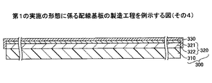
まず、図2(a)に示す工程では、上面が平坦面である支持体300を準備する。支持体300としては、例えば、プリプレグ310上にキャリア付き金属箔320が積層されたものを用いることができる。支持体300の厚さは、例えば18〜100μm程度とすることができる。
First, in the step shown in FIG. 2A, the
プリプレグ310は、例えば、ガラス繊維やアラミド繊維等の織布や不織布(図示せず)にエポキシ系樹脂等の絶縁樹脂を含侵させたものである。キャリア付き金属箔320は、銅からなる厚さ10〜50μm程度の厚箔(キャリア箔)322上に、剥離層(図示せず)を介して、銅からなる厚さ1.5〜5μm程度の薄箔321が剥離可能な状態で貼着されたものである。厚箔322は、薄箔321の取り扱いを容易にするための支持材として設けられている。厚箔322の下面は、プリプレグ310の上面に接着されている。
The
次に、図2(b)に示す工程では、支持体300を構成する薄箔321の上面に、例えば、キャリア付き金属箔320をめっき給電層に利用する電解めっき法等により、バリア層330を形成する。バリア層330は、後工程で薄箔321をエッチングで除去する際のエッチングストップ層となるものである。バリア層330の材料としては、銅からなる薄箔321のエッチング液で除去されない金属、例えば、ニッケル(Ni)等を用いることができる。バリア層330の厚さは、例えば、数μm程度とすることができる。
Next, in the step shown in FIG. 2B, the
次に、図2(c)に示す工程では、バリア層330の上面に、配線層10を形成する部分に開口部340xを備えたレジスト層340を形成する。具体的には、例えば、バリア層330の上面に、レジスト層340として感光性樹脂からなるドライフィルムレジストをラミネートする。そして、ドライフィルムレジストを露光及び現像によりパターニングし、配線層10を形成する部分にバリア層330の上面を露出する開口部340xを形成する。
Next, in a step shown in FIG. 2C, a resist
次に、図2(d)に示す工程では、キャリア付き金属箔320及びバリア層330をめっき給電層に利用する電解めっき法により、レジスト層340の開口部340x内に露出するバリア層330の上面に配線層10を形成する。配線層10は、一方の面がバリア層330の上面に接し、他方の面が開口部340x内に露出する。
Next, in the step shown in FIG. 2D, the upper surface of the
例えば、硫酸銅と硫酸を所定の濃度比で建浴した電解銅めっき液を用い、支持体300上に銅めっきを析出する。これにより、幅が広い部分であるパッド11及び12の層厚を厚く、幅が狭い部分である配線パターン13の層厚を薄く形成できる。この際、硫酸銅と硫酸の濃度比(硫酸銅/硫酸)を1以上とすることが好ましいが、硫酸銅と硫酸の濃度比(硫酸銅/硫酸)を5程度とすると、幅が狭い配線パターン13の部分の層厚を特に薄くできる点で好適である(後述の図14参照)。なお、パッド11、パッド12、及び配線パターン13の夫々の幅や層厚の数値例は、図1を参照して説明した通りである。
For example, copper plating is deposited on the
次に、図3(a)に示す工程では、図2(d)に示すレジスト層340を剥離する。レジスト層340は、例えば、水酸化ナトリウム等を含有する剥離液を用いて剥離できる。この際、幅の狭い配線パターン13の厚さが厚いと、狭ピッチ、高アスペクト比の配線パターンに挟まれ、狭ピッチ、高アスペクト比のレジストパターンが存在することになる。よって、前述のように、レジストパターンの剥離不良が発生し易くなる。
Next, in the step shown in FIG. 3A, the resist
しかし、本実施の形態では、図2(d)に示す工程において、めっき条件を調整することにより、配線パターン13の厚さを薄くしている。そのため、狭ピッチの配線パターン13に挟まれた狭ピッチ、高アスペクト比のレジストパターンにおいて、レジストパターン側面の、隣接する配線パターン13に挟み込まれる部分の面積を減少できる。
However, in the present embodiment, in the step shown in FIG. 2D, the thickness of the
その結果、レジストパターン側面と配線パターン13との接触面積が減少しているため、容易にレジストパターンを剥離できる。よって、剥離不良の発生を抑制できる。この効果は、ライン/スペース=8μm/8μm以下の、特にライン/スペースの狭い配線パターン13として形成される部分(例えば、図1(a)及び図1(b)の中央部分N)で顕著である。
As a result, since the contact area between the side surface of the resist pattern and the
なお、図3(a)に示す工程で、配線層10の他方の面及び側面に粗化処理を施してもよい。粗化処理は、例えば、蟻酸系水溶液、過酸化水素/硫酸系水溶液、過硫酸ナトリウム水溶液、過硫酸アンモニウム水溶液等への浸漬や、これら水溶液のスプレー処理により行うことができる。粗化処理により、配線層10の他方の面及び側面の表面粗さが、Ra=100nm〜500nm程度の範囲、例えばRa=300nmに粗化される。粗化処理により、配線層10と、後工程で形成される絶縁層20との密着性が向上する。又、配線層10の一方の面の粗度より、配線層10の他方の面及び側面の粗度が大きくなる。
In the step shown in FIG. 3A, the other surface and side surface of the
次に、図3(b)に示す工程では、バリア層330の上面に配線層10の他方の面及び側面を被覆する絶縁層20を形成する。具体的には、バリア層330の上面に配線層10を被覆するように、例えば熱硬化性を有するフィルム状のエポキシ系絶縁樹脂等をラミネートする。或いは、バリア層330の上面に配線層10を被覆するように、例えば熱硬化性を有する液状又はペースト状のエポキシ系絶縁樹脂等をスクリーン印刷、スピンコート法等により塗布する。そして、ラミネート又は塗布した絶縁樹脂を押圧しつつ、硬化温度以上に加熱して硬化させ、絶縁層20を作製する。必要に応じて、加圧しながら加熱してもよい。
Next, in a step shown in FIG. 3B, the insulating
次に、図3(c)に示す工程では、絶縁層20に、絶縁層20を貫通しパッド12の他方の面を露出させる開口部20xを形成する。開口部20xは、例えば、CO2レーザ等を用いたレーザ加工法により形成できる。絶縁層20を感光性樹脂により形成した場合には、感光性樹脂を露光及び現像することで絶縁層20に開口部20xを形成してもよい(フォトリソグラフィ法)。
Next, in the step shown in FIG. 3C, an
開口部20xをレーザ加工法により形成した場合には、デスミア処理を行い、開口部20x内に露出するパッド12の他方の面に付着した絶縁層20の樹脂残渣を除去することが好ましい。なお、レーザ光が照射される部分であるパッド12は厚く形成されているため、レーザ光がパッド12を貫通するおそれを低減できる。
When the
なお、樹脂残渣除去のため、デスミア処理に加え、ソフトエッチング処理により図3(c)の構造体の開口部20xに露出するパッド12の他方の面を除去し、凹部を形成してもよい。この処理を施して凹部が設けられても、パッド12は厚く形成されているため、パッド12が貫通するおそれがない。
In order to remove the resin residue, in addition to the desmear process, the other surface of the
次に、図3(d)に示す工程では、図3(c)に示す構造体から支持体300の一部を除去する。具体的には、支持体300に機械的な力を加え、キャリア付き金属箔320の薄箔321と厚箔322との界面を剥離する。前述のように、キャリア付き金属箔320は、薄箔321上に剥離層(図示せず)を介して厚箔322が貼着された構造を有するため、厚箔322は、剥離層(図示せず)とともに薄箔321から容易に剥離する。
Next, in the step shown in FIG. 3D, a part of the
これにより、薄箔321のみがバリア層330側に残り、支持体300を構成する他の部材(プリプレグ310及び厚箔322)が除去される。但し、剥離層とともに薄箔321から厚箔322が剥離する場合の他に、剥離層内で凝集破壊が起こり、薄箔321から厚箔322が剥離する場合もある。又、剥離層から厚箔322が剥離することで、薄箔321から厚箔322を剥離する場合もある。
As a result, only the
次に、図4(a)に示す工程では、エッチングにより銅からなる薄箔321(図3(d)参照)を除去する。銅からなる薄箔321は、例えば、過酸化水素/硫酸系水溶液や、過硫酸ナトリウム水溶液、過硫酸アンモニウム水溶液等を用いたウェットエッチングにより除去できる。なお、バリア層330がニッケル(Ni)からなる場合には、銅の上記エッチング液では除去されず、エッチングストップ層として機能するため、配線層10はエッチングされない。
Next, in the step shown in FIG. 4A, the
次に、図4(b)に示す工程では、バリア層330(図4(a)参照)を除去する。バリア層330がニッケル(Ni)からなる場合には、銅を除去せずにニッケル(Ni)を除去するエッチング液を選択することで、配線層10はエッチングせずにバリア層330のみをエッチングすることができる。これにより、絶縁層20の一方の面に配線層10の一方の面が露出する。配線層10の一方の面は、例えば、絶縁層20の一方の面と面一とすることができる。
Next, in the step shown in FIG. 4B, the barrier layer 330 (see FIG. 4A) is removed. When the
なお、必要に応じ、配線層10の一方の面、開口部20xから露出する配線層10のパッド12の他方の面に、例えば無電解めっき法等により金属層を形成してもよい。金属層の例としては、前述の通りである。又、金属層の形成に代えて、OSP処理等の酸化防止処理を施してもよい。
If necessary, a metal layer may be formed on one surface of the
図4(b)に示す工程の後、図4(b)に示す構造体をスライサー等により切断位置Cで切断して個片化することにより、複数の配線基板1(図1参照)が完成する。必要に応じ、パッド11上や、開口部20x内に露出するパッド12上に、はんだボール等の外部接続端子を設けてもよい。
After the step shown in FIG. 4B, the plurality of wiring boards 1 (see FIG. 1) are completed by cutting the structure shown in FIG. 4B at a cutting position C with a slicer or the like to divide it into individual pieces. To do. If necessary, an external connection terminal such as a solder ball may be provided on the
又、必要に応じ、図4(c)に示すように、配線基板1のチップ搭載面側に開口部40xを備えたソルダーレジスト層40を形成してもよい。ソルダーレジスト層40は、図4(b)に示す構造体をスライサー等により切断位置Cで切断する前に形成してもよいし、後に形成してもよい。
If necessary, as shown in FIG. 4C, a solder resist
ソルダーレジスト層40は、例えば、液状又はペースト状の絶縁樹脂を、スクリーン印刷法、ロールコート法、又は、スピンコート法等により、配線層10を被覆するように絶縁層20上に塗布することで形成できる。或いは、フィルム状の絶縁樹脂を、配線層10を被覆するように絶縁層20上にラミネートしてもよい。絶縁樹脂としては、例えば、感光性のエポキシ系絶縁樹脂やアクリル系絶縁樹脂等を用いることができる。
The solder resist
そして、塗布又はラミネートした絶縁樹脂を露光及び現像することでソルダーレジスト層40に配線層10のパッド11及び配線パターン13の一部を露出する開口部40xを形成することができる(フォトリソグラフィ法)。エポキシ系樹脂やポリイミド系樹脂を主成分とする非感光性の絶縁樹脂(熱硬化性樹脂)をソルダーレジスト層40の材料として用いた場合には、開口部40xをレーザ加工法やブラスト処理等により形成してもよい。
Then, by exposing and developing the applied or laminated insulating resin, the
なお、図3(a)に示す工程において配線層10の他方の面及び側面に粗化処理を施し、図3(c)に示す工程において開口部20xに露出するパッド12の他方の面にソフトエッチング処理を施した場合には、パッド12の近傍は、図4(d)のようになる。すなわち、パッド12を含む配線層10の他方の面及び側面は粗化面となり、開口部20xに露出するパッド12の他方の面には凹部12xが形成される。又、凹部12xの外縁部に、開口部20xの内壁よりも絶縁層20側に食い込んだアンダーカット12yが形成される。
In the step shown in FIG. 3A, the other surface and side surface of the
又、図2(b)に示す工程において、図5に示すように、支持体300を構成する薄箔321の上面と、キャリア付き金属箔320の側面(薄箔321の側面及び厚箔322の側面)とを連続的に被覆するように、バリア層330を形成してもよい。この構造は、配線基板1の製造工程中での不意のキャリア付き金属箔320の剥離を防止できる点で好適である。図5以降の工程は、図2(c)〜図4(b)と同様である。
Further, in the step shown in FIG. 2B, as shown in FIG. 5, the upper surface of the
このように、本実施の形態では、配線層10を、例えば、硫酸銅と硫酸を所定の濃度比で建浴した電解銅めっき液を用い、支持体300上に銅めっきを析出して形成する。これにより、配線層10のうち、幅が狭い配線パターン13の部分を薄く形成し、幅が広いパッド11及び12の部分を厚く形成することができる。
As described above, in the present embodiment, the
そのため、狭ピッチの配線パターン13に挟まれた狭ピッチ、高アスペクト比のレジストパターンにおいて、レジストパターン側面の、隣接する配線パターン13に挟み込まれる部分の面積を減少できる。その結果、レジストパターン側面と配線パターン13との接触面積が減少しているため、容易にレジストパターンを剥離できる。よって、剥離不良の発生を抑制できる。
Therefore, in a narrow-pitch, high-aspect-ratio resist pattern sandwiched between narrow-
特に、硫酸銅と硫酸の濃度比(硫酸銅/硫酸)を5程度とすると、幅が狭い配線パターン13の部分の層厚を特に薄くできる点で好適である。この場合、レジスト層340の剥離不良をいっそう低減できる。
In particular, it is preferable to set the concentration ratio of copper sulfate to sulfuric acid to about 5 (copper sulfate / sulfuric acid) because the layer thickness of the
又、パッド11及び12にはんだが形成される場合があるが、この場合、パッドとはんだとの界面に合金層が形成され、実質的にパッドの厚さが薄くなってパッドが脆くなる問題がある。配線基板1では、パッド11及び12を配線パターン13に比べて厚く形成しているため、合金層が形成されたとしても、合金層が形成されていない部分が多く残るため、合金層による影響を低減できる。
Further, solder may be formed on the
又、パッド11及び12を配線パターン13に比べて厚く形成しているため、例えば、パッド11又は12に対して無電解めっきの前処理で酸洗浄等を行った場合でも、パッドが過剰に薄くなることを防止できる。
Further, since the
〈第1の実施の形態の変形例1〉
第1の実施の形態の変形例1では、配線層10の一方の面と絶縁層20の一方の面との位置関係が第1の実施の形態とは異なる例を示す。なお、第1の実施の形態の変形例1において、既に説明した実施の形態と同一構成部についての説明は省略する場合がある。
<
図6は、第1の実施の形態の変形例1に係る配線基板を例示する断面図であり、図1(b)に対応する断面を示している。
FIG. 6 is a cross-sectional view illustrating a wiring board according to
図6を参照するに、配線基板2は、絶縁層20に凹部20yが形成され、配線層10の一方の面が凹部20y内において絶縁層20の一方の面よりも窪んだ位置に露出している点が、配線基板1(図1参照)と相違する。配線基板2は、例えば、以下に示す工程により製造できる。
Referring to FIG. 6, in
図7は、第1の実施の形態の変形例1に係る配線基板の製造工程を例示する図である。第1の実施の形態の変形例1では、支持体300上にバリア層330を形成しない。
FIG. 7 is a diagram illustrating a manufacturing process of the wiring board according to the first modification of the first embodiment. In the modified example 1 of the first embodiment, the
まず、図7(a)に示す工程では、図2(a)に示す工程の後、図2(c)〜図3(c)と同様の工程を実行し、支持体300上に、直接、配線層10及び絶縁層20を積層する。次に、図7(b)に示す工程では、図3(d)に示す工程と同様にして、図7(a)に示す構造体から支持体300を構成するプリプレグ310及び厚箔322を剥離する。これにより、薄箔321のみが絶縁層20側に残り、支持体300を構成する他の部材(プリプレグ310及び厚箔322)が除去される。
First, in the step shown in FIG. 7A, after the step shown in FIG. 2A, the same steps as those in FIGS. 2C to 3C are performed to directly and directly on the
次に、図7(c)に示す工程では、図4(a)に示す工程と同様にして、エッチングにより銅からなる薄箔321(図7(b)参照)を除去する。本実施の形態では、エッチングストップ層となるバリア層330が存在しないため、銅からなる配線層10の一方の面側もエッチングされ、絶縁層20の一方の面に凹部20yが形成される。そして、配線層10の一方の面が凹部20y内において絶縁層20の一方の面よりも窪んだ位置に露出する。
Next, in the step shown in FIG. 7C, similar to the step shown in FIG. 4A, the
図7(c)に示す工程の後、図7(c)に示す構造体をスライサー等により切断位置Cで切断して個片化することにより、複数の配線基板2が完成する。
After the step shown in FIG. 7C, the structure shown in FIG. 7C is cut into individual pieces by cutting at a cutting position C with a slicer or the like, whereby a plurality of
必要に応じ、配線層10の一方の面、開口部20xから露出する配線層10のパッド12の他方の面に、金属層等を形成してもよい。又、必要に応じ、パッド11上や、開口部20x内に露出するパッド12上に、はんだボール等の外部接続端子を設けてもよい。又、必要に応じ、配線基板2のチップ搭載面側に開口部40xを備えたソルダーレジスト層40を形成してもよい。
If necessary, a metal layer or the like may be formed on one surface of the
〈第1の実施の形態の変形例2〉
第1の実施の形態の変形例2では、配線基板1の製造方法の他の例を示す。なお、第1の実施の形態の変形例2において、既に説明した実施の形態と同一構成部についての説明は省略する場合がある。
<
The second modification of the first embodiment shows another example of the method for manufacturing the
図8は、第1の実施の形態の変形例2に係る配線基板の製造工程を例示する図である。第1の実施の形態の変形例2では、プリプレグ310上にキャリア付き金属箔320Aが積層された支持体300Aを用いる。キャリア付き金属箔320Aは、銅からなる厚さ10〜50μm程度の厚箔(キャリア箔)322上に、剥離層(図示せず)を介して、ニッケルからなる厚さ1.5〜5μm程度の薄箔321Aが剥離可能な状態で貼着されたものである。なお、薄箔321Aがエッチングストップ層となるため、支持体300Aにバリア層330を形成しない。
FIG. 8 is a diagram illustrating a manufacturing process of the wiring board according to the second modification of the first embodiment. In the second modification of the first embodiment, the
まず、図8(a)に示す工程では、図2(a)に示す工程と同様にして支持体300Aを作製後、図2(c)〜図3(c)と同様の工程を実行し、支持体300A上に、直接、配線層10及び絶縁層20を積層する。次に、図8(b)に示す工程では、図3(d)に示す工程と同様にして、図8(a)に示す構造体から支持体300Aを構成するプリプレグ310及び厚箔322を剥離する。これにより、薄箔321Aのみが絶縁層20側に残り、支持体300Aを構成する他の部材(プリプレグ310及び厚箔322)が除去される。
First, in the step shown in FIG. 8A, after the
次に、図8(c)に示す工程では、エッチングによりニッケルからなる薄箔321A(図8(b)参照)を除去する。銅を除去せずにニッケル(Ni)を除去するエッチング液を選択することで、配線層10はエッチングせずに薄箔321Aのみをエッチングすることができる。これにより、絶縁層20の一方の面に配線層10の一方の面が露出する。配線層10の一方の面は、例えば、絶縁層20の一方の面と面一とすることができる。
Next, in the step shown in FIG. 8C, the
図8(c)に示す工程の後、図8(c)に示す構造体をスライサー等により切断位置Cで切断して個片化することにより、複数の配線基板1(図1参照)が完成する。 After the step shown in FIG. 8C, the plurality of wiring boards 1 (see FIG. 1) are completed by cutting the structure shown in FIG. To do.
必要に応じ、配線層10の一方の面、開口部20xから露出する配線層10のパッド12の他方の面に、金属層等を形成してもよい。又、必要に応じ、パッド11上や、開口部20x内に露出するパッド12上に、はんだボール等の外部接続端子を設けてもよい。又、必要に応じ、配線基板1のチップ搭載面側に開口部40xを備えたソルダーレジスト層40を形成してもよい。
If necessary, a metal layer or the like may be formed on one surface of the
〈第1の実施の形態の変形例3〉
第1の実施の形態の変形例3では、絶縁層20の他方の面に支持体(キャリア)を設けた例を示す。なお、第1の実施の形態の変形例3において、既に説明した実施の形態と同一構成部についての説明は省略する場合がある。
<
図9は、第1の実施の形態の変形例3に係る配線基板を例示する断面図であり、図1(b)に対応する断面を示している。
FIG. 9 is a cross-sectional view illustrating a wiring board according to
図9を参照するに、配線基板3は、絶縁層20の他方の面に粘着層50を介して支持体60が設けられている点が、配線基板1(図1参照)と相違する。配線基板3は、例えば、以下に示す工程により製造できる。
Referring to FIG. 9,
図10は、第1の実施の形態の変形例3に係る配線基板の製造工程を例示する図である。 FIG. 10 is a diagram illustrating a manufacturing process of the wiring board according to the modified example 3 of the first embodiment.
まず、図10(a)に示す工程では、図2(a)〜図3(c)と同様の工程を実行し、図3(c)の構造体の絶縁層20の他方の面に粘着層50を介して支持体60を設ける。粘着層50としては、例えば、アクリル系、シリコーン系、エポキシ系等の樹脂を用いることができる。支持体60としては、例えば、金属箔(例えば、銅箔)、樹脂フィルム(例えば、ポリイミドフィルム)、樹脂基板(例えば、ガラスエポキシ基板)等を用いることができる。
First, in the step illustrated in FIG. 10A, the same steps as those in FIGS. 2A to 3C are performed, and the adhesive layer is formed on the other surface of the insulating
なお、後述のように、粘着層50及び支持体60を備えた配線基板3に半導体チップを実装する場合があるため、粘着層50及び支持体60は、リフロー等の実装工程における加熱に耐える耐熱性を有している必要がある。
As will be described later, since the semiconductor chip may be mounted on the
次に、図10(b)に示す工程では、図3(d)に示す工程と同様にして、図10(a)に示す構造体から支持体300を構成するプリプレグ310及び厚箔322を剥離する。これにより、薄箔321のみがバリア層330側に残り、支持体300を構成する他の部材(プリプレグ310及び厚箔322)が除去される。
Next, in the step shown in FIG. 10B, similar to the step shown in FIG. 3D, the
次に、図10(c)に示す工程では、図4(a)に示す工程と同様にして、エッチングにより銅からなる薄箔321(図10(b)参照)を除去する。次に、図10(d)に示す工程では、図4(b)に示す工程と同様にして、バリア層330(図10(c)参照)を除去する。これにより、絶縁層20の一方の面に配線層10の一方の面が露出する。配線層10の一方の面は、例えば、絶縁層20の一方の面と面一とすることができる。
Next, in the step shown in FIG. 10C, similar to the step shown in FIG. 4A, the
図10(d)に示す工程の後、図10(d)に示す構造体をスライサー等により切断位置Cで切断して個片化することにより、複数の配線基板3が完成する。
After the step illustrated in FIG. 10D, the plurality of
必要に応じ、図10(a)に示す工程よりも前に、配線層10の一方の面、開口部20xから露出する配線層10のパッド12の他方の面に、金属層等を形成してもよい。又、必要に応じ、図10(d)に示す工程よりも後に、配線基板3のチップ搭載面側に開口部40xを備えたソルダーレジスト層40を形成してもよい。又、図2(a)に示す工程で用いる支持体に代えて、図5に示す支持体を用いてもよい。
If necessary, a metal layer or the like is formed on one surface of the
又、必要に応じ、図3(c)の構造体に支持体60を設けて図10(a)の構造体とする前に、図3(c)の構造体の開口部20xに露出するパッド12の他方の面に、無電解めっき法等により金属層を形成したり、OSP処理等の酸化防止処理を施してもよい。又、必要に応じ、図10(d)の構造体において、配線層10の一方の面に、無電解めっき法等により金属層を形成したり、OSP処理等の酸化防止処理を施してもよい。
If necessary, before the
又、図10(c)に示す構造体、すなわち、バリア層330が設けられた状態の支持体60付き配線基板を製品出荷形態としてもよい。又、図10(c)に示す構造体又は図10(d)に示す構造体は、個片化前の状態を製品出荷形態としてもよいし、個片化後の状態を製品出荷形態としてもよい。
Further, the structure shown in FIG. 10C, that is, the wiring board with the
配線基板3は、絶縁層20の他方の面に支持体60が設けられているため、配線基板3全体の剛性を高めることができる。そのため、例えば、後述の図12に示すように、配線基板3の出荷後に半導体チップを実装する際の取り扱いが容易となる。
Since the
なお、図6に示す配線基板2に支持体60を設けてもよい。又、配線基板2の製造途中の構造体を用い、図10の工程を行ってもよい。
The
〈配線基板の応用例1〉
配線基板の応用例1では、第1の実施の形態に係る配線基板に半導体チップが搭載(フリップチップ実装)された半導体パッケージの例を示す。なお、配線基板の応用例1において、既に説明した実施の形態と同一構成部についての説明は省略する場合がある。
<Application example 1 of wiring board>
Application Example 1 of the wiring board shows an example of a semiconductor package in which a semiconductor chip is mounted (flip-chip mounted) on the wiring board according to the first embodiment. In the application example 1 of the wiring board, the description of the same components as those in the above-described embodiments may be omitted.
図11は、応用例1に係る半導体パッケージを例示する断面図である。図11を参照するに、半導体パッケージ4は、図1に示す配線基板1と、半導体チップ100と、バンプ110と、アンダーフィル樹脂120と、封止樹脂130とを有する。
FIG. 11 is a cross-sectional view illustrating a semiconductor package according to Application Example 1. Referring to FIG. 11, the
半導体チップ100は、例えば、シリコン等からなる薄板化された半導体基板(図示せず)上に半導体集積回路(図示せず)等が形成されたものである。半導体基板(図示せず)には、半導体集積回路(図示せず)と電気的に接続された電極パッド(図示せず)が形成されている。
The
バンプ110は、半導体チップ100の電極パッド(図示せず)と、配線基板1のパッド11とを電気的に接続している。バンプ110は、例えば、はんだバンプである。はんだバンプの材料としては、例えばPbを含む合金、SnとCuの合金、SnとAgの合金、SnとAgとCuの合金等を用いることができる。
The
アンダーフィル樹脂120は、半導体チップ100と配線基板1(絶縁層20)との間に充填されている。アンダーフィル樹脂120としては、例えば、フィラーを含有していない熱硬化性のエポキシ系樹脂等の絶縁樹脂を用いることができる。
The
封止樹脂130は、半導体チップ100とアンダーフィル樹脂120を被覆するように配線基板1上に形成されている。但し、封止樹脂130の上面に半導体チップ100の上面(背面)を露出させてもよい。封止樹脂130としては、例えば、フィラーを含有した熱硬化性のエポキシ系樹脂等の絶縁樹脂(所謂モールド樹脂)を用いることができる。
The sealing
但し、アンダーフィル樹脂120は、必要に応じて設ければよい。又、封止樹脂130は設けずに、アンダーフィル樹脂120のみを設けてもよい。
However, the
半導体パッケージ4を作製するには、例えば、配線基板1のチップ搭載面に、ペースト状のバンプ110を介して半導体チップ100をフェースダウンで搭載する。そして、リフロー等により、バンプ110を溶融後凝固させ、半導体チップ100の電極パッド(図示せず)と、配線基板1のパッド11とを電気的に接続する。
To manufacture the
その後、半導体チップ100と配線基板1(絶縁層20)との間に必要に応じてアンダーフィル樹脂120を充填後、半導体チップ100とアンダーフィル樹脂120を被覆するように配線基板1上に封止樹脂130を形成する。封止樹脂130は、例えば、封止金型を用いたトランスファーモールド法等により形成することができる。必要に応じ、開口部20x内に露出するパッド12上に、はんだボール等の外部接続端子を設けてもよい。
Thereafter, an
なお、半導体パッケージ4において、配線基板1に代えて配線基板2又は3を用いてもよい。配線基板3を用いる場合には、図12(a)に示すように、図10(d)の工程を経た配線基板3を個片化せずに、配線基板3となる各領域のチップ搭載面に、ペースト状のバンプ110を介して半導体チップ100をフェースダウンで搭載する。そして、リフロー等により、バンプ110を溶融後凝固させ、半導体チップ100の電極パッド(図示せず)と、配線基板3となる各領域のパッド11とを電気的に接続する。そして、半導体チップ100と絶縁層20との間に必要に応じてアンダーフィル樹脂120を充填する。なお、図10と図12とは、配線基板の上下が反転した状態で描かれている。
In the
次に、図12(b)に示すように、図12(a)に示す支持体60に機械的な力を加え、粘着層50及び支持体60を絶縁層20の下面から剥離する。
Next, as shown in FIG. 12B, a mechanical force is applied to the
次に、図12(c)に示すように、半導体チップ100とアンダーフィル樹脂120を被覆するように配線基板3となる各領域上にトランスファーモールド法等により封止樹脂130を形成する。
Next, as shown in FIG. 12C, a sealing
図12(c)に示す工程の後、図12(c)に示す構造体をスライサー等により切断位置Cで切断して個片化することにより、複数の半導体パッケージ4(図11参照)が完成する。必要に応じ、開口部20x内に露出するパッド12上に、はんだボール等の外部接続端子を設けてもよい。
After the step shown in FIG. 12C, the structure shown in FIG. 12C is cut into individual pieces by cutting at a cutting position C with a slicer or the like to complete a plurality of semiconductor packages 4 (see FIG. 11). To do. If necessary, an external connection terminal such as a solder ball may be provided on the
なお、支持体60を設けた状態で封止樹脂130を形成し、その後、支持体60を除去し、個片化を行い、複数の半導体パッケージ4を形成してもよい。つまり、図12(a)の状態で封止樹脂130を形成して図12(d)の状態とし、その後、支持体60の除去を行って図12(c)の状態とし、個片化を行い、複数の半導体パッケージ4を形成してもよい。この場合は、封止樹脂130を形成後に支持体60を除去するため、配線基板の剛性が低い場合でも配線基板の変形を防止できる。
Note that the plurality of
このように、配線基板1〜3に半導体チップ100を搭載することにより、半導体パッケージ4を実現できる。
In this way, the
ところで、パッド11が、幅の異なる複数種類のパッドを含んでいる場合がある。この場合、幅が異なるパッドは厚さも異なるが(幅が広い方が厚くなる)、パッド11の半導体チップ100を搭載する側の面は同一平面にある。そのため、パッド11の厚さが異なっても、各パッド11と半導体チップ100の各電極パッドとのギャップは一定となり、各パッド11と半導体チップ100の各電極パッドとを容易に接続することができる。
By the way, the
〈配線基板の応用例2〉
配線基板の応用例2では、半導体パッケージ上に更に他の半導体パッケージが搭載された所謂POP(Package on package)構造の半導体パッケージの例を示す。なお、配線基板の応用例2において、既に説明した実施の形態と同一構成部についての説明は省略する場合がある。
<Wiring board application example 2>
Application example 2 of the wiring board shows an example of a semiconductor package having a so-called POP (Package on package) structure in which another semiconductor package is mounted on the semiconductor package. In application example 2 of the wiring board, description of the same components as those in the above-described embodiments may be omitted.
図13は、応用例2に係る半導体パッケージを例示する断面図である。図13を参照するに、半導体パッケージ5は、半導体チップ100を実装した配線基板1上に、更に半導体チップ100を実装した配線基板1がバンプ90を介して搭載された、所謂POP構造の半導体パッケージである。バンプ90としては、例えば、銅コアボールの周囲をはんだで覆った構造のはんだボールを用いることができる。なお、半導体パッケージ5において、配線基板1に代えて配線基板2又は3を用いてもよい。
FIG. 13 is a cross-sectional view illustrating a semiconductor package according to Application Example 2. Referring to FIG. 13, the
半導体パッケージ5を作製するには、例えば、図12(b)に示す構造体を2個作製する。そして、一方の図12(b)に示す構造体上に、銅コアボールの周囲をはんだで覆った構造のはんだボールを搭載し、更に他方の図12(b)に示す構造体を搭載する。この際、一方の図12(b)に示す構造体のパッド12の上面と他方の図12(b)に示す構造体の開口部20x内のパッド12の下面とが、はんだボールを介して対向するように配置する。
To manufacture the
次に、他方の図12(b)に示す構造体を一方の図12(b)に示す構造体に対して押圧しながらリフローを行い、銅コアボールの周囲のはんだを溶融後凝固させて、銅コアボールを介して上下のパッド12同士を接合する。この際、銅コアボールが上下のパッド12と接した状態ではんだが凝固するため、銅コアボールがスペーサ部材として機能し、他方の図12(b)に示す構造体と一方の図12(b)に示す構造体との間隔が所定値に維持される。
Next, reflow is performed while pressing the other structure shown in FIG. 12 (b) against one structure shown in FIG. 12 (b), and the solder around the copper core balls is melted and solidified, The upper and
その後、一方の図12(b)に示す構造体及び他方の図12(b)に示す構造体の各半導体チップ100と各アンダーフィル樹脂120を被覆するようにトランスファーモールド法等により封止樹脂130を形成する。その後、スライサー等により個片化することにより、複数の半導体パッケージ5(図13参照)が完成する。必要に応じ、一方の図12(b)に示す構造体の開口部20x内に露出するパッド12上に、はんだボール等の外部接続端子を設けてもよい。
Thereafter, the sealing
このように、第1の実施の形態に係る配線基板1〜3を用いて、POP構造の半導体パッケージ5を実現できる。
In this way, the
[実施例1]
配線幅が狭い部分(ここではファインライン部と称する)と、配線幅が広い部分(ここではラフライン部と称する)について、電解銅めっきの条件を変更して、形成された配線のめっき厚の検討を行った。
[Example 1]
Examination of the plating thickness of the formed wiring by changing the conditions of electrolytic copper plating for a portion with a narrow wiring width (herein referred to as a fine line portion) and a portion with a wide wiring width (herein referred to as a rough line portion) I went.
ここでは、ファインライン部のライン/スペースを10μm/10μm、ラフライン部のライン/スペースを25μm/25μmとした。 Here, the line / space of the fine line portion was 10 μm / 10 μm, and the line / space of the rough line portion was 25 μm / 25 μm.
まず、導体層を設けた基板上に、ライン/スペース=10μm/10μmのファインライン部と、ライン/スペース=25μm/25μmのラフライン部とを形成するための開口部を備えたレジスト層を作製した。 First, a resist layer having an opening for forming a fine line portion of line / space = 10 μm / 10 μm and a rough line portion of line / space = 25 μm / 25 μm was produced on a substrate provided with a conductor layer. .
次に、硫酸銅と硫酸を濃度比1で建浴した電解銅めっき液と、濃度比5で建浴した電解銅めっき液とを用意した。そして、夫々の電解銅めっき液を用い、電流密度を1.0ASD(A/dm2)、めっき時間を60分として電解めっきを行い、ファインライン部及びラフライン部に対応するレジスト層の開口部内に電解銅めっき膜を析出した。 Next, an electrolytic copper plating solution prepared by bathing copper sulfate and sulfuric acid at a concentration ratio of 1 and an electrolytic copper plating solution prepared by bathing at a concentration ratio of 5 were prepared. Then, using each of the electrolytic copper plating solutions, electrolytic plating was performed at a current density of 1.0 ASD (A / dm 2 ) and a plating time of 60 minutes, and the electrolytic plating was performed in the openings of the resist layer corresponding to the fine line portion and the rough line portion. An electrolytic copper plating film was deposited.
又、比較例1として、硫酸銅と硫酸を濃度比0.2で建浴した電解銅めっき液と、濃度比5.5で建浴した電解銅めっき液とを用意した。そして、実施例1と同様に、夫々の電解銅めっき液を用い、電流密度を1.0ASD、めっき時間を60分として電解めっきを行い、ファインライン部及びラフライン部に対応するレジスト層の開口部内に電解銅めっき膜を析出した。 In addition, as Comparative Example 1, an electrolytic copper plating solution in which copper sulfate and sulfuric acid were bathed at a concentration ratio of 0.2 and an electrolytic copper plating solution in which a bath was concentrated at a concentration ratio of 5.5 were prepared. Then, in the same manner as in Example 1, electrolytic plating was performed using each electrolytic copper plating solution with a current density of 1.0 ASD and a plating time of 60 minutes, and inside the openings of the resist layer corresponding to the fine line portion and the rough line portion. An electrolytic copper plating film was deposited on.
結果を図14に示す。図14よりわかるように、硫酸銅と硫酸との濃度比を1とした場合には、ファインライン部のめっき厚は平均値で13μm程度、ラフライン部のめっき厚は平均値で15μm程度となり、両者の差異は2μm程度であった。又、硫酸銅と硫酸との濃度比を5とした場合には、ファインライン部のめっき厚は平均値で12μm程度、ラフライン部のめっき厚は平均値で15.5μm程度となり、両者の差異は3.5μm程度であった。つまり、何れの濃度比でも、ファインライン部とラフライン部で、平均値で1μm以上の十分なめっき厚差が得られた。 The results are shown in Fig. 14. As can be seen from FIG. 14, when the concentration ratio of copper sulfate to sulfuric acid is 1, the average plating thickness of the fine line portion is about 13 μm and the average plating thickness of the rough line portion is about 15 μm. Was about 2 μm. When the concentration ratio of copper sulfate to sulfuric acid is 5, the average thickness of the fine line is 12 μm and the average thickness of the rough line is 15.5 μm. It was about 3.5 μm. That is, at any of the concentration ratios, a sufficient plating thickness difference of 1 μm or more was obtained between the fine line portion and the rough line portion on average.
これに対して、比較例1で硫酸銅と硫酸との濃度比を0.2とした場合には、ファインライン部のめっき厚は平均値で14μm程度、ラフライン部のめっき厚は平均値で14.5μm程度となり、両者の差異は0.5μm程度であった。又、比較例1で硫酸銅と硫酸との濃度比を0.2とした場合には、銅イオンの供給不足のため、電解銅めっきの異常析出が生じていた。なお、比較例1で硫酸銅と硫酸との濃度比を5.5とした場合には、銅イオンの供給過剰のため、電解銅めっきの異常析出が生じ、めっき厚を計測することができず、図14に結果を示すことができなかった。 On the other hand, when the concentration ratio of copper sulfate to sulfuric acid is 0.2 in Comparative Example 1, the fine line portion has an average plating thickness of about 14 μm, and the rough line portion has an average plating thickness of 14 μm. It was about 0.5 μm, and the difference between the two was about 0.5 μm. Further, when the concentration ratio of copper sulfate to sulfuric acid was set to 0.2 in Comparative Example 1, abnormal deposition of electrolytic copper plating occurred due to insufficient supply of copper ions. When the concentration ratio of copper sulfate to sulfuric acid was set to 5.5 in Comparative Example 1, abnormal deposition of electrolytic copper plating occurred due to excessive supply of copper ions, and the plating thickness could not be measured. The results could not be shown in FIG.
このように、硫酸銅と硫酸との濃度比が0.2以下、又は5.5以上では電解銅めっき膜の品質を確保できないため、硫酸銅と硫酸との濃度比は0.2よりも大きく5以下であることが好ましい。又、ファインライン部とラフライン部で平均値で1μm以上の顕著なめっき厚差が得られる、硫酸銅と硫酸との濃度比が1以上5以下の範囲が特に好ましい。 Thus, if the concentration ratio of copper sulfate to sulfuric acid is 0.2 or less, or 5.5 or more, the quality of the electrolytic copper plating film cannot be ensured, so the concentration ratio of copper sulfate to sulfuric acid is larger than 0.2. It is preferably 5 or less. Further, it is particularly preferable that the concentration ratio of copper sulfate to sulfuric acid is 1 or more and 5 or less so that a remarkable difference in plating thickness of 1 μm or more can be obtained on the average between the fine line portion and the rough line portion.
[実施例2]
レジスト層のアスペクト比を1〜4まで0.5置きに変えたサンプルを作製した。そして、硫酸銅と硫酸を濃度比5で建浴した電解銅めっき液を用い、電流密度を1.0ASD、めっき時間を60分として、アスペクト比の異なるレジスト層を用いて電解めっきを行った。その後、レジスト層を剥離し、レジスト剥離の不良率を測定した。
[Example 2]
Samples were prepared in which the aspect ratio of the resist layer was changed from 1 to 4 at intervals of 0.5. Then, electrolytic plating was carried out using a resist layer having different aspect ratios, using an electrolytic copper plating solution prepared by bathing copper sulfate and sulfuric acid at a concentration ratio of 5 with a current density of 1.0 ASD and a plating time of 60 minutes. Then, the resist layer was peeled off, and the defect rate of resist peeling was measured.
又、比較例2として、硫酸銅と硫酸を濃度比0.2未満で建浴した電解銅めっき液を用い、電流密度を1.0ASD、めっき時間を60分として、アスペクト比の異なるレジスト層を用いて電解めっきを行った。その後、レジスト層を剥離し、レジスト剥離の不良率を測定した。 Further, as Comparative Example 2, using an electrolytic copper plating solution in which copper sulfate and sulfuric acid were formed in a concentration ratio of less than 0.2, the current density was 1.0 ASD, and the plating time was 60 minutes to form resist layers having different aspect ratios. It was used for electrolytic plating. Then, the resist layer was peeled off, and the defect rate of resist peeling was measured.
結果を図15に示す。図15よりわかるように、実施例2では、レジスト層のアスペクト比が3.5までは不良率が0%であり、レジスト層のアスペクト比が4では不良率が約10%であった。これに対して、比較例2では、レジスト層のアスペクト比が3.5では不良率が約5%であり、レジスト層のアスペクト比が4では不良率が約50%であった。 The results are shown in Fig. 15. As can be seen from FIG. 15, in Example 2, the defect rate was 0% until the aspect ratio of the resist layer was 3.5, and when the aspect ratio of the resist layer was 4, the defect rate was about 10%. On the other hand, in Comparative Example 2, when the aspect ratio of the resist layer was 3.5, the defective rate was about 5%, and when the aspect ratio of the resist layer was 4, the defective rate was about 50%.
このように、レジスト層のアスペクト比が高い部分(すなわち、ファインライン部)におけるめっき厚を薄くすることにより、レジスト剥離の不良率を大幅に低減できることが確認された。 As described above, it was confirmed that the defective rate of resist peeling can be significantly reduced by reducing the plating thickness in the portion having a high aspect ratio of the resist layer (that is, the fine line portion).
以上、好ましい実施の形態等について詳説したが、上述した実施の形態等に制限されることはなく、特許請求の範囲に記載された範囲を逸脱することなく、上述した実施の形態等に種々の変形及び置換を加えることができる。 Although the preferred embodiments and the like have been described in detail above, the present invention is not limited to the above-described embodiments and the like, and various embodiments and the like described above are possible without departing from the scope described in the claims. Modifications and substitutions can be added.
例えば、上記実施の形態では、配線層の幅が狭い部分の例として配線パターンを、幅が広い部分の例としてパッドを挙げたが、これには限定されない。例えば、幅が広い部分の例として、電源やグラウンドのプレーン層を挙げることができる。又、配線パターンの中に、幅が狭い配線パターンと、幅が広い配線パターンとが混在してもよい。 For example, in the above-described embodiment, the wiring pattern is given as an example of the portion where the width of the wiring layer is narrow, and the pad is given as an example of the portion where the width is wide. However, the present invention is not limited to this. For example, a plane layer of a power supply or a ground can be given as an example of the wide portion. Further, a wiring pattern having a narrow width and a wiring pattern having a wide width may be mixed in the wiring pattern.
又、配線基板の製造方法において、プリプレグ310の両面にキャリア付き金属箔320や320Aを積層して支持体とし、支持体の両面上に配線基板を形成してもよい。
In the method for manufacturing a wiring board, the metal foils 320 and 320A with a carrier may be laminated on both surfaces of the
1、2、3 配線基板
4、5 半導体パッケージ
10 配線層
11、12 パッド
12x、20y 凹部
12y アンダーカット
13 配線パターン
20 絶縁層
20x、40x、340x 開口部
40 ソルダーレジスト層
50 粘着層
60、300、300A 支持体
90、110 バンプ
100 半導体チップ
120 アンダーフィル樹脂
130 封止樹脂
310 プリプレグ
320、320A キャリア付き金属箔
321、321A 薄箔
322 厚箔
330 バリア層
340 レジスト層
1, 2 and 3
Claims (10)
前記絶縁層の一方の面側に埋め込まれた銅からなる配線層と、を有し、
前記配線層は、第1の部分と、前記第1の部分よりも幅及び間隔が広い第2の部分と、を備え、
前記第1の部分は、前記第2の部分よりも層厚が1.0μm以上薄く形成されており、
前記第1の部分の一方の面及び前記第2の部分の一方の面は、前記絶縁層の一方の面から露出し、
前記第2の部分の他方の面の一部は、前記絶縁層の他方の面側に開口する開口部内に露出している配線基板。 An insulating layer,
A wiring layer made of copper embedded on one surface side of the insulating layer,
The wiring layer includes a first portion and a second portion having a width and a spacing wider than that of the first portion,
The first portion has a layer thickness of 1.0 μm or more smaller than that of the second portion,
One surface of the first portion and one surface of the second portion are exposed from one surface of the insulating layer,
A wiring board in which a part of the other surface of the second portion is exposed in an opening opening to the other surface of the insulating layer.
前記第2の部分の側面及び他方の面は前記絶縁層に被覆され、
前記第2の部分の他方の面の一部が前記開口部内に露出している請求項1又は2に記載の配線基板。 The side surface and the other surface of the first portion are covered with the insulating layer,
The side surface and the other surface of the second portion are covered with the insulating layer,
The wiring board according to claim 1, wherein a part of the other surface of the second portion is exposed in the opening.
前記開口部内に露出する部分に設けられた外部接続用のパッドと、
該外部接続用のパッドと異なる部分に設けられた半導体チップ接続用のパッドと、を含む請求項4に記載の配線基板。 The pad is
A pad for external connection provided in a portion exposed in the opening,
The wiring board according to claim 4, further comprising a pad for connecting a semiconductor chip, which is provided in a portion different from the pad for external connection.
前記支持体上に、前記第1の部分及び前記第2の部分を被覆するように、一方の面が前記支持体と接する絶縁層を形成する工程と、
前記絶縁層に、前記絶縁層の他方の面側に開口し前記第2の部分の他方の面の一部を露出する開口部を形成する工程と、
前記支持体を除去する工程と、を有し、
前記配線層を形成する工程では、前記第1の部分は、前記第2の部分よりも層厚が1.0μm以上薄く形成される配線基板の製造方法。 A plating is deposited on a support, and a first portion and a second portion having a width and a spacing larger than that of the first portion are provided, and one of the first portion and the second portion is provided. Forming a wiring layer made of copper, the surface of which is in contact with the support,
Forming an insulating layer on the support, one surface of which is in contact with the support, so as to cover the first portion and the second portion;
Forming an opening in the insulating layer on the other surface side of the insulating layer and exposing a part of the other surface of the second portion;
A step of removing the support,
The method of manufacturing a wiring board, wherein in the step of forming the wiring layer, the first portion has a layer thickness thinner than that of the second portion by 1.0 μm or more .
硫酸銅と硫酸を所定の濃度比で建浴した電解銅めっき液を用いた電解めっき法により、前記第1の部分及び前記第2の部分を銅めっきで形成し、
前記所定の濃度比を予め調整することで、前記第1の部分の層厚を前記第2の部分の層厚よりも薄く形成する請求項8又は9に記載の配線基板の製造方法。 In the step of forming the wiring layer,
The first portion and the second portion are formed by copper plating by an electrolytic plating method using an electrolytic copper plating solution in which copper sulfate and sulfuric acid are bathed at a predetermined concentration ratio,
The method for manufacturing a wiring board according to claim 8, wherein the layer thickness of the first portion is formed thinner than the layer thickness of the second portion by adjusting the predetermined concentration ratio in advance.
Priority Applications (2)
| Application Number | Priority Date | Filing Date | Title |
|---|---|---|---|
| JP2016137740A JP6689691B2 (en) | 2016-07-12 | 2016-07-12 | Wiring board and manufacturing method thereof |
| US15/645,017 US10170405B2 (en) | 2016-07-12 | 2017-07-10 | Wiring substrate and semiconductor package |
Applications Claiming Priority (1)
| Application Number | Priority Date | Filing Date | Title |
|---|---|---|---|
| JP2016137740A JP6689691B2 (en) | 2016-07-12 | 2016-07-12 | Wiring board and manufacturing method thereof |
Publications (3)
| Publication Number | Publication Date |
|---|---|
| JP2018010931A JP2018010931A (en) | 2018-01-18 |
| JP2018010931A5 JP2018010931A5 (en) | 2019-04-04 |
| JP6689691B2 true JP6689691B2 (en) | 2020-04-28 |
Family
ID=60940698
Family Applications (1)
| Application Number | Title | Priority Date | Filing Date |
|---|---|---|---|
| JP2016137740A Active JP6689691B2 (en) | 2016-07-12 | 2016-07-12 | Wiring board and manufacturing method thereof |
Country Status (2)
| Country | Link |
|---|---|
| US (1) | US10170405B2 (en) |
| JP (1) | JP6689691B2 (en) |
Families Citing this family (2)
| Publication number | Priority date | Publication date | Assignee | Title |
|---|---|---|---|---|
| JP7384820B2 (en) * | 2018-11-15 | 2023-11-21 | ローム株式会社 | semiconductor equipment |
| KR20200073051A (en) | 2018-12-13 | 2020-06-23 | 엘지이노텍 주식회사 | Printed circuit board |
Family Cites Families (11)
| Publication number | Priority date | Publication date | Assignee | Title |
|---|---|---|---|---|
| US4811081A (en) * | 1987-03-23 | 1989-03-07 | Motorola, Inc. | Semiconductor die bonding with conductive adhesive |
| JP2641869B2 (en) * | 1987-07-24 | 1997-08-20 | 三菱電機株式会社 | Method for manufacturing semiconductor device |
| KR920702545A (en) * | 1990-06-26 | 1992-09-04 | 아이자와 스스무 | Semiconductor device and manufacturing method thereof |
| US5678301A (en) * | 1991-06-04 | 1997-10-21 | Micron Technology, Inc. | Method for forming an interconnect for testing unpackaged semiconductor dice |
| KR0153387B1 (en) * | 1993-12-16 | 1998-12-01 | 가네꼬 히사시 | Chip carrier semiconductor device assembly and its manufacture |
| JPH08236586A (en) * | 1994-12-29 | 1996-09-13 | Nitto Denko Corp | Semiconductor device and manufacturing method thereof |
| JPH08288424A (en) * | 1995-04-18 | 1996-11-01 | Nec Corp | Semiconductor device |
| US6114763A (en) * | 1997-05-30 | 2000-09-05 | Tessera, Inc. | Semiconductor package with translator for connection to an external substrate |
| US6140707A (en) * | 1998-05-07 | 2000-10-31 | 3M Innovative Properties Co. | Laminated integrated circuit package |
| US6100112A (en) * | 1998-05-28 | 2000-08-08 | The Furukawa Electric Co., Ltd. | Method of manufacturing a tape carrier with bump |
| JP5003812B2 (en) | 2009-12-10 | 2012-08-15 | イビデン株式会社 | Printed wiring board and printed wiring board manufacturing method |
-
2016
- 2016-07-12 JP JP2016137740A patent/JP6689691B2/en active Active
-
2017
- 2017-07-10 US US15/645,017 patent/US10170405B2/en active Active
Also Published As
| Publication number | Publication date |
|---|---|
| JP2018010931A (en) | 2018-01-18 |
| US20180019196A1 (en) | 2018-01-18 |
| US10170405B2 (en) | 2019-01-01 |
Similar Documents
| Publication | Publication Date | Title |
|---|---|---|
| US9515018B2 (en) | Wiring substrate and method for manufacturing wiring substrate | |
| US10892216B2 (en) | Wiring substrate and semiconductor device | |
| US9997441B2 (en) | Support member, wiring substrate, method for manufacturing wiring substrate, and method for manufacturing semiconductor package | |
| KR101968957B1 (en) | Wiring substrate, method for manufacturing the wiring substrate, and semiconductor package | |
| JP6691451B2 (en) | Wiring board, manufacturing method thereof, and electronic component device | |
| JP6223909B2 (en) | Wiring board and manufacturing method thereof | |
| JP2015079795A (en) | Wiring board, semiconductor device and wiring board manufacturing method | |
| US9334576B2 (en) | Wiring substrate and method of manufacturing wiring substrate | |
| JP2017073520A (en) | Wiring board, semiconductor device, and manufacturing method of wiring board | |
| JP6510897B2 (en) | Wiring board, method of manufacturing the same and electronic component device | |
| JP2018026437A (en) | Wiring board and manufacturing method of the same | |
| JP6632302B2 (en) | Wiring board and manufacturing method thereof | |
| JP4170266B2 (en) | Wiring board manufacturing method | |
| JP6689691B2 (en) | Wiring board and manufacturing method thereof | |
| US10811348B2 (en) | Method of manufacturing wiring substrate | |
| JP6457881B2 (en) | Wiring board and manufacturing method thereof | |
| KR100925669B1 (en) | Method of fabricating a solder on pad for coreless package substrate technology | |
| JP2005243986A (en) | Method for manufacturing wiring board | |
| JP2005243990A (en) | Method for manufacturing wiring board | |
| KR101314712B1 (en) | Thin PCB substrate having via layer and method of manufacturing the same | |
| JP2012248891A (en) | Wiring board and manufacturing method of the same | |
| JP2019016683A (en) | Wiring board and manufacturing method of the same, and semiconductor package | |
| JP2017112199A (en) | Wiring board and semiconductor device |
Legal Events
| Date | Code | Title | Description |
|---|---|---|---|
| A521 | Request for written amendment filed |
Free format text: JAPANESE INTERMEDIATE CODE: A523 Effective date: 20190221 |
|
| A621 | Written request for application examination |
Free format text: JAPANESE INTERMEDIATE CODE: A621 Effective date: 20190221 |
|
| A977 | Report on retrieval |
Free format text: JAPANESE INTERMEDIATE CODE: A971007 Effective date: 20191121 |
|
| A131 | Notification of reasons for refusal |
Free format text: JAPANESE INTERMEDIATE CODE: A131 Effective date: 20191126 |
|
| A521 | Request for written amendment filed |
Free format text: JAPANESE INTERMEDIATE CODE: A523 Effective date: 20200115 |
|
| TRDD | Decision of grant or rejection written | ||
| A01 | Written decision to grant a patent or to grant a registration (utility model) |
Free format text: JAPANESE INTERMEDIATE CODE: A01 Effective date: 20200324 |
|
| A61 | First payment of annual fees (during grant procedure) |
Free format text: JAPANESE INTERMEDIATE CODE: A61 Effective date: 20200408 |
|
| R150 | Certificate of patent or registration of utility model |
Ref document number: 6689691 Country of ref document: JP Free format text: JAPANESE INTERMEDIATE CODE: R150 |