JP6664278B2 - Display device - Google Patents
Display device Download PDFInfo
- Publication number
- JP6664278B2 JP6664278B2 JP2016108187A JP2016108187A JP6664278B2 JP 6664278 B2 JP6664278 B2 JP 6664278B2 JP 2016108187 A JP2016108187 A JP 2016108187A JP 2016108187 A JP2016108187 A JP 2016108187A JP 6664278 B2 JP6664278 B2 JP 6664278B2
- Authority
- JP
- Japan
- Prior art keywords
- touch
- base film
- display device
- region
- unit
- Prior art date
- Legal status (The legal status is an assumption and is not a legal conclusion. Google has not performed a legal analysis and makes no representation as to the accuracy of the status listed.)
- Active
Links
- 238000000034 method Methods 0.000 claims description 42
- 239000000758 substrate Substances 0.000 claims description 41
- 238000004519 manufacturing process Methods 0.000 claims description 27
- 230000000149 penetrating effect Effects 0.000 claims 1
- 239000002585 base Substances 0.000 description 74
- 239000010410 layer Substances 0.000 description 72
- 239000011229 interlayer Substances 0.000 description 28
- 239000004065 semiconductor Substances 0.000 description 22
- 229910052751 metal Inorganic materials 0.000 description 15
- 239000002184 metal Substances 0.000 description 15
- 239000012790 adhesive layer Substances 0.000 description 10
- 238000005192 partition Methods 0.000 description 10
- 238000002161 passivation Methods 0.000 description 9
- 239000012212 insulator Substances 0.000 description 7
- 238000004544 sputter deposition Methods 0.000 description 7
- 229910052581 Si3N4 Inorganic materials 0.000 description 6
- HQVNEWCFYHHQES-UHFFFAOYSA-N silicon nitride Chemical compound N12[Si]34N5[Si]62N3[Si]51N64 HQVNEWCFYHHQES-UHFFFAOYSA-N 0.000 description 6
- XUIMIQQOPSSXEZ-UHFFFAOYSA-N Silicon Chemical compound [Si] XUIMIQQOPSSXEZ-UHFFFAOYSA-N 0.000 description 5
- 238000005229 chemical vapour deposition Methods 0.000 description 5
- 239000000463 material Substances 0.000 description 5
- 230000001681 protective effect Effects 0.000 description 5
- 229910052710 silicon Inorganic materials 0.000 description 5
- 239000010703 silicon Substances 0.000 description 5
- 239000002356 single layer Substances 0.000 description 5
- 229910052782 aluminium Inorganic materials 0.000 description 4
- XAGFODPZIPBFFR-UHFFFAOYSA-N aluminium Chemical compound [Al] XAGFODPZIPBFFR-UHFFFAOYSA-N 0.000 description 4
- 230000015572 biosynthetic process Effects 0.000 description 4
- 239000012535 impurity Substances 0.000 description 4
- 239000002861 polymer material Substances 0.000 description 4
- 239000011347 resin Substances 0.000 description 4
- 229920005989 resin Polymers 0.000 description 4
- VYPSYNLAJGMNEJ-UHFFFAOYSA-N silicon dioxide Inorganic materials O=[Si]=O VYPSYNLAJGMNEJ-UHFFFAOYSA-N 0.000 description 4
- 239000004925 Acrylic resin Substances 0.000 description 3
- 229920000178 Acrylic resin Polymers 0.000 description 3
- GYHNNYVSQQEPJS-UHFFFAOYSA-N Gallium Chemical compound [Ga] GYHNNYVSQQEPJS-UHFFFAOYSA-N 0.000 description 3
- 239000004642 Polyimide Substances 0.000 description 3
- 239000000956 alloy Substances 0.000 description 3
- 229910045601 alloy Inorganic materials 0.000 description 3
- 239000004020 conductor Substances 0.000 description 3
- 238000001312 dry etching Methods 0.000 description 3
- 229910052733 gallium Inorganic materials 0.000 description 3
- 229910052738 indium Inorganic materials 0.000 description 3
- APFVFJFRJDLVQX-UHFFFAOYSA-N indium atom Chemical compound [In] APFVFJFRJDLVQX-UHFFFAOYSA-N 0.000 description 3
- 229910010272 inorganic material Inorganic materials 0.000 description 3
- 239000011147 inorganic material Substances 0.000 description 3
- 239000004973 liquid crystal related substance Substances 0.000 description 3
- 239000003550 marker Substances 0.000 description 3
- -1 polycrystal Substances 0.000 description 3
- 229920000728 polyester Polymers 0.000 description 3
- 229920001721 polyimide Polymers 0.000 description 3
- 229910052814 silicon oxide Inorganic materials 0.000 description 3
- 229910052709 silver Inorganic materials 0.000 description 3
- 239000004332 silver Substances 0.000 description 3
- RYGMFSIKBFXOCR-UHFFFAOYSA-N Copper Chemical compound [Cu] RYGMFSIKBFXOCR-UHFFFAOYSA-N 0.000 description 2
- ZOKXTWBITQBERF-UHFFFAOYSA-N Molybdenum Chemical compound [Mo] ZOKXTWBITQBERF-UHFFFAOYSA-N 0.000 description 2
- 239000004952 Polyamide Substances 0.000 description 2
- RTAQQCXQSZGOHL-UHFFFAOYSA-N Titanium Chemical compound [Ti] RTAQQCXQSZGOHL-UHFFFAOYSA-N 0.000 description 2
- 230000000903 blocking effect Effects 0.000 description 2
- 229910052802 copper Inorganic materials 0.000 description 2
- 239000010949 copper Substances 0.000 description 2
- 230000000694 effects Effects 0.000 description 2
- 239000003822 epoxy resin Substances 0.000 description 2
- 238000005530 etching Methods 0.000 description 2
- 239000011521 glass Substances 0.000 description 2
- 229910052750 molybdenum Inorganic materials 0.000 description 2
- 239000011733 molybdenum Substances 0.000 description 2
- 238000001020 plasma etching Methods 0.000 description 2
- 229920002647 polyamide Polymers 0.000 description 2
- 229920000515 polycarbonate Polymers 0.000 description 2
- 239000004417 polycarbonate Substances 0.000 description 2
- 229920000647 polyepoxide Polymers 0.000 description 2
- 229920001296 polysiloxane Polymers 0.000 description 2
- 239000002994 raw material Substances 0.000 description 2
- 238000000926 separation method Methods 0.000 description 2
- 239000000126 substance Substances 0.000 description 2
- 229910052719 titanium Inorganic materials 0.000 description 2
- 239000010936 titanium Substances 0.000 description 2
- WFKWXMTUELFFGS-UHFFFAOYSA-N tungsten Chemical compound [W] WFKWXMTUELFFGS-UHFFFAOYSA-N 0.000 description 2
- 229910052721 tungsten Inorganic materials 0.000 description 2
- 239000010937 tungsten Substances 0.000 description 2
- 239000004215 Carbon black (E152) Substances 0.000 description 1
- YCKRFDGAMUMZLT-UHFFFAOYSA-N Fluorine atom Chemical compound [F] YCKRFDGAMUMZLT-UHFFFAOYSA-N 0.000 description 1
- FYYHWMGAXLPEAU-UHFFFAOYSA-N Magnesium Chemical compound [Mg] FYYHWMGAXLPEAU-UHFFFAOYSA-N 0.000 description 1
- BLRPTPMANUNPDV-UHFFFAOYSA-N Silane Chemical compound [SiH4] BLRPTPMANUNPDV-UHFFFAOYSA-N 0.000 description 1
- HCHKCACWOHOZIP-UHFFFAOYSA-N Zinc Chemical compound [Zn] HCHKCACWOHOZIP-UHFFFAOYSA-N 0.000 description 1
- 229910052783 alkali metal Inorganic materials 0.000 description 1
- 150000001340 alkali metals Chemical class 0.000 description 1
- 150000004703 alkoxides Chemical class 0.000 description 1
- 230000004888 barrier function Effects 0.000 description 1
- 229910052795 boron group element Inorganic materials 0.000 description 1
- 239000003990 capacitor Substances 0.000 description 1
- 229910052800 carbon group element Inorganic materials 0.000 description 1
- 239000000919 ceramic Substances 0.000 description 1
- 230000008878 coupling Effects 0.000 description 1
- 238000010168 coupling process Methods 0.000 description 1
- 238000005859 coupling reaction Methods 0.000 description 1
- 239000013078 crystal Substances 0.000 description 1
- 238000001514 detection method Methods 0.000 description 1
- 238000010586 diagram Methods 0.000 description 1
- 238000003618 dip coating Methods 0.000 description 1
- 230000005674 electromagnetic induction Effects 0.000 description 1
- 239000011737 fluorine Substances 0.000 description 1
- 229910052731 fluorine Inorganic materials 0.000 description 1
- 229910001849 group 12 element Inorganic materials 0.000 description 1
- 238000010438 heat treatment Methods 0.000 description 1
- 229930195733 hydrocarbon Natural products 0.000 description 1
- 150000002430 hydrocarbons Chemical class 0.000 description 1
- AMGQUBHHOARCQH-UHFFFAOYSA-N indium;oxotin Chemical compound [In].[Sn]=O AMGQUBHHOARCQH-UHFFFAOYSA-N 0.000 description 1
- 238000002347 injection Methods 0.000 description 1
- 239000007924 injection Substances 0.000 description 1
- 238000010030 laminating Methods 0.000 description 1
- 229910052749 magnesium Inorganic materials 0.000 description 1
- 239000011777 magnesium Substances 0.000 description 1
- 239000011159 matrix material Substances 0.000 description 1
- 230000008018 melting Effects 0.000 description 1
- 238000002844 melting Methods 0.000 description 1
- 150000002739 metals Chemical class 0.000 description 1
- 239000013081 microcrystal Substances 0.000 description 1
- 239000003595 mist Substances 0.000 description 1
- 230000007935 neutral effect Effects 0.000 description 1
- 239000011368 organic material Substances 0.000 description 1
- 230000001151 other effect Effects 0.000 description 1
- 239000004033 plastic Substances 0.000 description 1
- 230000000379 polymerizing effect Effects 0.000 description 1
- 239000010453 quartz Substances 0.000 description 1
- 238000007789 sealing Methods 0.000 description 1
- 229910000077 silane Inorganic materials 0.000 description 1
- 125000000123 silicon containing inorganic group Chemical group 0.000 description 1
- 238000003980 solgel method Methods 0.000 description 1
- 238000004528 spin coating Methods 0.000 description 1
- 229910052715 tantalum Inorganic materials 0.000 description 1
- GUVRBAGPIYLISA-UHFFFAOYSA-N tantalum atom Chemical compound [Ta] GUVRBAGPIYLISA-UHFFFAOYSA-N 0.000 description 1
- 229920001187 thermosetting polymer Polymers 0.000 description 1
- 229910052725 zinc Inorganic materials 0.000 description 1
- 239000011701 zinc Substances 0.000 description 1
- YVTHLONGBIQYBO-UHFFFAOYSA-N zinc indium(3+) oxygen(2-) Chemical compound [O--].[Zn++].[In+3] YVTHLONGBIQYBO-UHFFFAOYSA-N 0.000 description 1
Images


Classifications
-
- H—ELECTRICITY
- H10—SEMICONDUCTOR DEVICES; ELECTRIC SOLID-STATE DEVICES NOT OTHERWISE PROVIDED FOR
- H10K—ORGANIC ELECTRIC SOLID-STATE DEVICES
- H10K59/00—Integrated devices, or assemblies of multiple devices, comprising at least one organic light-emitting element covered by group H10K50/00
- H10K59/40—OLEDs integrated with touch screens
-
- G—PHYSICS
- G06—COMPUTING; CALCULATING OR COUNTING
- G06F—ELECTRIC DIGITAL DATA PROCESSING
- G06F3/00—Input arrangements for transferring data to be processed into a form capable of being handled by the computer; Output arrangements for transferring data from processing unit to output unit, e.g. interface arrangements
- G06F3/01—Input arrangements or combined input and output arrangements for interaction between user and computer
- G06F3/03—Arrangements for converting the position or the displacement of a member into a coded form
- G06F3/041—Digitisers, e.g. for touch screens or touch pads, characterised by the transducing means
- G06F3/0412—Digitisers structurally integrated in a display
-
- G—PHYSICS
- G06—COMPUTING; CALCULATING OR COUNTING
- G06F—ELECTRIC DIGITAL DATA PROCESSING
- G06F3/00—Input arrangements for transferring data to be processed into a form capable of being handled by the computer; Output arrangements for transferring data from processing unit to output unit, e.g. interface arrangements
- G06F3/01—Input arrangements or combined input and output arrangements for interaction between user and computer
- G06F3/03—Arrangements for converting the position or the displacement of a member into a coded form
- G06F3/041—Digitisers, e.g. for touch screens or touch pads, characterised by the transducing means
- G06F3/0414—Digitisers, e.g. for touch screens or touch pads, characterised by the transducing means using force sensing means to determine a position
-
- G—PHYSICS
- G06—COMPUTING; CALCULATING OR COUNTING
- G06F—ELECTRIC DIGITAL DATA PROCESSING
- G06F3/00—Input arrangements for transferring data to be processed into a form capable of being handled by the computer; Output arrangements for transferring data from processing unit to output unit, e.g. interface arrangements
- G06F3/01—Input arrangements or combined input and output arrangements for interaction between user and computer
- G06F3/03—Arrangements for converting the position or the displacement of a member into a coded form
- G06F3/041—Digitisers, e.g. for touch screens or touch pads, characterised by the transducing means
- G06F3/0416—Control or interface arrangements specially adapted for digitisers
- G06F3/04164—Connections between sensors and controllers, e.g. routing lines between electrodes and connection pads
-
- G—PHYSICS
- G06—COMPUTING; CALCULATING OR COUNTING
- G06F—ELECTRIC DIGITAL DATA PROCESSING
- G06F3/00—Input arrangements for transferring data to be processed into a form capable of being handled by the computer; Output arrangements for transferring data from processing unit to output unit, e.g. interface arrangements
- G06F3/01—Input arrangements or combined input and output arrangements for interaction between user and computer
- G06F3/03—Arrangements for converting the position or the displacement of a member into a coded form
- G06F3/041—Digitisers, e.g. for touch screens or touch pads, characterised by the transducing means
- G06F3/044—Digitisers, e.g. for touch screens or touch pads, characterised by the transducing means by capacitive means
- G06F3/0443—Digitisers, e.g. for touch screens or touch pads, characterised by the transducing means by capacitive means using a single layer of sensing electrodes
-
- G—PHYSICS
- G06—COMPUTING; CALCULATING OR COUNTING
- G06F—ELECTRIC DIGITAL DATA PROCESSING
- G06F3/00—Input arrangements for transferring data to be processed into a form capable of being handled by the computer; Output arrangements for transferring data from processing unit to output unit, e.g. interface arrangements
- G06F3/01—Input arrangements or combined input and output arrangements for interaction between user and computer
- G06F3/03—Arrangements for converting the position or the displacement of a member into a coded form
- G06F3/041—Digitisers, e.g. for touch screens or touch pads, characterised by the transducing means
- G06F3/044—Digitisers, e.g. for touch screens or touch pads, characterised by the transducing means by capacitive means
- G06F3/0446—Digitisers, e.g. for touch screens or touch pads, characterised by the transducing means by capacitive means using a grid-like structure of electrodes in at least two directions, e.g. using row and column electrodes
-
- H—ELECTRICITY
- H10—SEMICONDUCTOR DEVICES; ELECTRIC SOLID-STATE DEVICES NOT OTHERWISE PROVIDED FOR
- H10K—ORGANIC ELECTRIC SOLID-STATE DEVICES
- H10K71/00—Manufacture or treatment specially adapted for the organic devices covered by this subclass
-
- G—PHYSICS
- G06—COMPUTING; CALCULATING OR COUNTING
- G06F—ELECTRIC DIGITAL DATA PROCESSING
- G06F2203/00—Indexing scheme relating to G06F3/00 - G06F3/048
- G06F2203/041—Indexing scheme relating to G06F3/041 - G06F3/045
- G06F2203/04102—Flexible digitiser, i.e. constructional details for allowing the whole digitising part of a device to be flexed or rolled like a sheet of paper
-
- G—PHYSICS
- G06—COMPUTING; CALCULATING OR COUNTING
- G06F—ELECTRIC DIGITAL DATA PROCESSING
- G06F2203/00—Indexing scheme relating to G06F3/00 - G06F3/048
- G06F2203/041—Indexing scheme relating to G06F3/041 - G06F3/045
- G06F2203/04103—Manufacturing, i.e. details related to manufacturing processes specially suited for touch sensitive devices
-
- G—PHYSICS
- G06—COMPUTING; CALCULATING OR COUNTING
- G06F—ELECTRIC DIGITAL DATA PROCESSING
- G06F2203/00—Indexing scheme relating to G06F3/00 - G06F3/048
- G06F2203/041—Indexing scheme relating to G06F3/041 - G06F3/045
- G06F2203/04111—Cross over in capacitive digitiser, i.e. details of structures for connecting electrodes of the sensing pattern where the connections cross each other, e.g. bridge structures comprising an insulating layer, or vias through substrate
Landscapes
- Engineering & Computer Science (AREA)
- General Engineering & Computer Science (AREA)
- Theoretical Computer Science (AREA)
- Human Computer Interaction (AREA)
- Physics & Mathematics (AREA)
- General Physics & Mathematics (AREA)
- Computer Networks & Wireless Communication (AREA)
- Manufacturing & Machinery (AREA)
- Devices For Indicating Variable Information By Combining Individual Elements (AREA)
- Electroluminescent Light Sources (AREA)
- Liquid Crystal (AREA)
Description
本発明の実施形態の一つは、有機EL表示装置などの表示装置とその作製方法に関する。例えば、タッチパネルが搭載された表示装置、およびその作製方法に関する。 One embodiment of the present invention relates to a display device such as an organic EL display device and a manufacturing method thereof. For example, the present invention relates to a display device provided with a touch panel and a method for manufacturing the display device.
ユーザが表示装置に対して情報を入力するためのインターフェースとして、タッチパネルが知られている。タッチパネルを表示装置の画面上に設置することで、画面上に表示される入力ボタンやアイコンなどをユーザが操作することができ、表示装置へ容易に情報を入力することができる。例えば特許文献1や2では、液晶表示装置上にタッチパネルが搭載された積層型表示装置が開示されている。
A touch panel is known as an interface for a user to input information to a display device. By installing the touch panel on the screen of the display device, the user can operate input buttons, icons, and the like displayed on the screen, and can easily input information to the display device. For example,
本発明は、低コストで作製可能な、タッチパネルが搭載された表示装置、ならびにその作製方法を提供することを課題の一つとする。 An object of the present invention is to provide a display device provided with a touch panel, which can be manufactured at low cost, and a manufacturing method thereof.
本発明の実施形態の一つは、表示領域、タッチ領域、表示領域とタッチ領域の間の境界領域を有するベースフィルムと、表示領域上の、ベースフィルムの第1面側に形成された画像表示部と、タッチ領域上の、ベースフィルムの第2面側に形成されたタッチ部を有する表示装置である。境界領域は、画像表示部とタッチ部に挟まれ、境界領域において、タッチ部の正面がタッチ部を介して画像表示部と重なるように、ベースフィルムが折りたたまれる。タッチ部の正面は、タッチ部の互いに対向する二つの面のうち、ベースフィルムに遠い面である。 One embodiment of the present invention is a base film having a display region, a touch region, a boundary region between the display region and the touch region, and an image display formed on the first surface side of the base film on the display region. The display device includes a portion and a touch portion formed on the second surface side of the base film on the touch area. The boundary region is sandwiched between the image display unit and the touch unit. In the boundary region, the base film is folded such that the front of the touch unit overlaps the image display unit via the touch unit. The front surface of the touch unit is a surface far from the base film among the two opposing surfaces of the touch unit.
本発明の実施形態の一つは、表示領域、タッチ領域、表示領域とタッチ領域の間の境界領域を有するベースフィルムと、表示領域上の画像表示部と、タッチ領域上のタッチ部を有する表示装置である。表示装置は、表示領域上に位置し、表示領域から境界領域を介してタッチ領域に伸びる配線によってタッチ部と電気的に接続される端子を有する。境界領域において、タッチ部の正面がタッチ部を介して画像表示部と重なるように、ベースフィルムが折りたたまれる。タッチ部の正面は、タッチ部の互いに対向する二つの面のうち、ベースフィルムに遠い面である。 One embodiment of the present invention is a display having a display region, a touch region, a base film having a boundary region between the display region and the touch region, an image display portion on the display region, and a display having a touch portion on the touch region. Device. The display device has a terminal located on the display area and electrically connected to the touch unit by a wiring extending from the display area to the touch area via the boundary area. In the boundary region, the base film is folded such that the front of the touch unit overlaps the image display unit via the touch unit. The front surface of the touch unit is a surface far from the base film among the two opposing surfaces of the touch unit.
本発明の実施形態の一つは、ベースフィルムの第1面側に画像表示部を形成し、ベースフィルムの第2面側にタッチ部を形成し、タッチ部が画像表示部と重なり、画像表示部がベースフィルムに包まれるように、ベースフィルムを折りたたむことを含む、表示装置の作製方法である。 One embodiment of the present invention is to form an image display unit on a first surface side of a base film, form a touch unit on a second surface side of the base film, and the touch unit overlaps the image display unit to display an image. It is a manufacturing method of a display device including folding a base film so that a part may be wrapped in a base film.
以下、本発明の各実施形態について、図面等を参照しつつ説明する。但し、本発明は、その要旨を逸脱しない範囲において様々な態様で実施することができ、以下に例示する実施形態の記載内容に限定して解釈されるものではない。 Hereinafter, embodiments of the present invention will be described with reference to the drawings and the like. However, the present invention can be carried out in various modes without departing from the gist of the present invention, and is not to be construed as being limited to the description of the embodiments exemplified below.
図面は、説明をより明確にするため、実際の態様に比べ、各部の幅、厚さ、形状等について模式的に表される場合があるが、あくまで一例であって、本発明の解釈を限定するものではない。本明細書と各図において、既出の図に関して説明したものと同様の機能を備えた要素には、同一の符号を付して、重複する説明を省略することがある。 The drawings may be schematically illustrated in terms of width, thickness, shape, and the like of each portion as compared with actual embodiments in order to make the description clearer, but are merely examples, and the interpretation of the present invention is limited. It does not do. In the present specification and each drawing, elements having the same functions as those described in relation to the already described drawings are denoted by the same reference numerals, and redundant description may be omitted.
本発明において、ある一つの膜を加工して複数の膜を形成した場合、これら複数の膜は異なる機能、役割を有することがある。しかしながら、これら複数の膜は同一の工程で同一層として形成された膜に由来し、同一の層構造、同一の材料を有する。したがって、これら複数の膜は同一層に存在しているものと定義する。 In the present invention, when a certain film is processed to form a plurality of films, the plurality of films may have different functions and roles. However, these multiple films are derived from films formed as the same layer in the same step, and have the same layer structure and the same material. Therefore, these multiple films are defined as existing in the same layer.
本明細書および特許請求の範囲において、ある構造体の上に他の構造体を配置する態様を表現するにあたり、単に「上に」と表記する場合、特に断りの無い限りは、ある構造体に接するように、直上に他の構造体を配置する場合と、ある構造体の上方に、さらに別の構造体を介して他の構造体を配置する場合との両方を含むものとする。 In this specification and the claims, in describing the mode of arranging another structure on a certain structure, when simply written as "on", unless otherwise specified, a certain structure may be used. This includes both a case where another structure is arranged directly above and a case where another structure is arranged above a certain structure via another structure.
(第1実施形態)
[1.全体構造]
本実施形態では、本発明の実施形態の表示装置100の構造に関し、図1乃至図6を用いて説明する。
(1st Embodiment)
[1. Overall structure]
In the present embodiment, the structure of the
表示装置100の上面模式図を図1(A)、(B)に、図1(A)の鎖線A−A’に沿った断面模式図を図2に示す。図2に示すように、表示装置100はベースフィルム102を有し、ベースフィルム102は表示領域120、タッチ領域140、および表示領域120とタッチ領域140の間の境界領域160を有する。タッチ領域140は表示領域120の上に位置し、表示領域120と重なる。境界領域160は表示領域120とタッチ領域140を接続する。ベースフィルム102は可撓性を有する板、あるいは膜であり、可視光に対して透過性を有する。
FIGS. 1A and 1B are schematic top views of the
表示領域120には、ベースフィルム102上に画像表示部122が設けられる。後述するように、画像表示部122には複数の画素が設けられる。表示領域120には画素を駆動するための駆動回路などを備えることができ、複数の画素によって画像表示部122上に映像が再現される。
In the
タッチ領域140には、ベースフィルム102の上にタッチ部142が設けられる。タッチ部142は画像表示部122と同じ、あるいは実質的に同じ大きさ、形状であり画像表示部122と重なる(図1(A))。後述するように、タッチ部142は、指や掌などの物体と接触(以下、タッチと記す)することでタッチを感知し、その位置を特定する機能を有しており、ユーザによる情報入力のインターフェースとして働く。タッチ部142には、例えば静電容量方式、抵抗膜方式、電磁誘導方式などを採用することができる。図1(A)に示すように、ユーザはタッチ部142を介して画像表示部122を認識する。
In the
上述したように、境界領域160において、表示領域120内のベースフィルム102とタッチ領域140内のベースフィルム102が接続される。換言すると、境界領域160内のベースフィルム102、表示領域120内のベースフィルム102、およびタッチ領域140内のベースフィルム102は一体化されており、表示領域120内のベースフィルム102は、画像表示部122の下から、境界領域160を経てタッチ領域140のタッチ部142の下へ伸びる。したがって、表示領域120、境界領域160、タッチ領域140のベースフィルム102は連続した構造を有しており、画像表示部122はベースフィルム102によって包まれている。さらに、ベースフィルム102の一部、すなわち、タッチ領域140内のベースフィルム102は、画像表示部122とタッチ部142によって挟持される。
As described above, in the
表示領域120はさらに、複数の第1の端子124と複数の第2の端子126をベースフィルム102の上に有している(図1(A)、(B)、図2)。複数の第1の端子124と複数の第2の端子126の各々は、少なくともその一部がタッチ領域140のベースフィルム102と重ならないように設けられる。すなわち、複数の第1の端子124と複数の第2の端子126の各々はいずれも、少なくとも一部はタッチ領域140のベースフィルム102から露出される。
The
第1の端子124と第2の端子126は、画像表示部122の一つの辺(第1の辺)128の近傍に、第1の辺128とほぼ平行に配置される。第1の端子124は、ベースフィルム102上に設けられる配線130を介し、画像表示部122と電気的に接続される。一方、第2の端子126は、表示領域120内のベースフィルム102上に設けられる配線132を介し、タッチ部142と電気的に接続される。図1(A)では、複数の第2の端子126が複数の第1の端子124を挟むように示されているが、複数の第2の端子126の全てが一か所に纏まって設けられてもよい。
The
図1(B)に示すように、第1の端子124と第2の端子126は、フレキシブルプリント回路基板(FPC)などのコネクタ170と接続され、コネクタ170、第1の端子124、第2の端子126を通して外部回路から画像表示部122、タッチ部142へ信号が入力される。例えば第1の端子124には映像信号や電源が供給され、第2の端子126には、タッチを検出するための検出信号などが供給される。
As shown in FIG. 1B, the
上述したように、第1の端子124と第2の端子126はいずれも表示領域120内のベースフィルム102上に設けられ、かつ、第1の辺128の近傍に、第1の辺128に対して平行に設けられる。したがって、第1の端子124と第2の端子126は単一のコネクタ170と接続することができる。このため、第1の端子124と第2の端子126をそれぞれ異なるコネクタに接続する場合と比較し、コネクタの数を半減することができるため、製造コストを低下させ、製造プロセスをより簡潔にすることができる。
As described above, both the
表示領域120とタッチ領域140は互いに接着していてもよい。例えば図2に示すように、表示領域120とタッチ領域140は、接着層182、184を介して互いに接着されていてもよい。この時、任意の構成として、透明基板180を表示領域120とタッチ領域140の間に設け、表示装置100の厚さを調整してもよい。この場合、透明基板180は画像表示部122と、タッチ領域140のベースフィルム102と接着される。透明基板180は可視光に対して透光性を示すことが好ましい。透明基板180は可撓性を有してもよい。なお、透明基板180による境界領域160内のベースフィルム102の損傷を防ぐため、透明基板180の端部のうち境界領域160に近い側の先端が丸い形状を有するように面取りされていてもよい。
The
[2.タッチ部]
図3にタッチ部142の一部の領域144(図1(A)参照)の拡大図を模式的に示す。タッチ部142は種々の方式でタッチを検出することができるが、ここでは静電容量式のタッチ部を例として説明する。
[2. Touch section]
FIG. 3 schematically shows an enlarged view of a partial area 144 (see FIG. 1A) of the
タッチ部142は複数の配線が格子状に配置された構造を有している。具体的には、第1の方向(例えば第1の辺128に平行な方向、図1参照)に伸びる複数の配線(Tx配線146)と、これらと直交する複数の配線(Rx配線148)を有している。各配線は、略四角形の複数の電極150を含んでいる。例えばTx配線146の各々は、複数の電極150が第1の方向に配列し、隣接する電極150同士はTxブリッジ電極(接続電極)152で電気的に接続される。図3では、Txブリッジ電極152の上に電極150が形成される例が示されている。Tx配線146の末端の電極(図3における左端の電極)には、配線接続部154が設けられる。この配線接続部154において、配線133がTx配線146と電気的に接続される。Rx配線148は、複数の電極150と、各電極150間を接続するRxブリッジ部156が一体となって形成された構造を有している。Rx配線148の末端の電極(図3における下端の電極)には、配線接続部154が設けられる。Tx配線146と同様、Rx配線148の配線接続部154において、配線133がRx配線148と電気的に接続される。
The
各電極150、およびRxブリッジ部156は、例えば導電性酸化物などの可視光を透過する導電体で形成される。一方、Txブリッジ電極は、必ずしも可視光を透過する必要は無く、透光性を有する導電性酸化物に加え、可視光を透過しない金属で形成してもよい。
Each of the
[3.展開構造]
表示装置100の構造をより詳細に説明するため、表示装置100の展開された状態を図4に示す。図4は、図2に示した表示装置100から透明基板180と接着層182、184を除去し、境界領域160を平坦にした状態を示したものである。
[3. Deployment Structure]
In order to explain the structure of the
図4に示すように、ベースフィルム102は表示領域120とタッチ領域140を有し、表示領域120とタッチ領域140の間に境界領域160を有する。タッチ領域140には、ベースフィルム102の下にタッチ部142が備えられる。一方、表示領域120には、ベースフィルム102の上に画像表示部122が設けられる。したがって、画像表示部122はベースフィルム102の一方の面(第1面)に設けられ、タッチ部142はベースフィルム102の他方の面(第1面に対向する第2面)に設けられる。図4に示す表示装置100では、表示領域120に駆動回路136が画像表示部122を挟むように設けられているが、駆動回路136は任意の構成であり、異なる基板に形成された駆動回路136を別途表示装置100に設けてもよい。この場合、駆動回路136は、例えば配線130の上、あるいはコネクタ170の上などに設けることができる。
As shown in FIG. 4, the
配線132は、第2の端子126と接続され、画像表示部122の横の領域(額縁)を通り、境界領域160を介して表示領域120からタッチ領域140へ伸びる。配線132はさらに、タッチ領域140内でベースフィルム102に設けられる開口部158において、ベースフィルム102の下面に設けられる配線133と電気的に接続される。上述したように配線133はタッチ部142のTx配線146やRx配線148と接続される。したがって、タッチ部142は配線133、132を介し、第2の端子126と電気的に接続される。一方、配線130は第1の端子124と画像表示部122を電気的に接続する。図示しないが、配線132、133は境界領域160において、画像表示部122やタッチ部142への各辺に対して斜めの方向に伸びるように配置してもよい。
The
ベースフィルム102上にはアライメントマーカー134を設けることができる。アライメントマーカー134が重なるように軸162に沿って境界領域160を折りたたみ、表示領域120とタッチ領域140を接着することによって、図1(A)、(B)、図2に示す表示装置100を得ることができる。
An
[4.画像表示部]
図5に画像表示部122の一部の領域138(図4参照)の拡大図を模式的に示す。画像表示部122は複数の画素190を有している。複数の画素190には発光素子や液晶素子などの表示素子を設けることができる。例えば隣接する画素190が赤色、緑色、あるいは青色を与えるように構成することで、フルカラー表示を行うことができる。画素190の配列にも制限はなく、ストライプ配列、デルタ配列、ペンタイル配列などを採用することができる。ペンタイル配列とは、ストライプ配列やデルタ配列に比べて少ない画素数で見かけ上の精細度を向上させる効果のある配列であり、例えばRGBの一部の画素を縦横方向のマトリクス配置とする一方、他の一部の画素は、斜め方向に先の一部の画素と互い違いになるように配置する。RGB間でサブピクセル数が異なる等の特徴がある。
[4. Image display section]
FIG. 5 schematically shows an enlarged view of a partial area 138 (see FIG. 4) of the
各画素190には一つ、あるいは複数のトランジスタが備えられ、それぞれのトランジスタに信号を与える複数の信号線192、194,196が格子状に設けられる。例えば信号線194は映像信号を、信号線192は走査信号を、信号線196は高電位電源電圧を各画素190に供給することができる。図示しないが、画像表示部122には上記配線以外の配線を有していてもよい。これらの配線は駆動回路136、あるいは配線130を介して第1の端子124と接続される。
Each
[5.断面構造]
[5−1.表示領域]
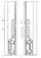
図6を用い、表示装置100の断面構造を詳細に説明する。図6は、図1(A)の鎖線B−B’に沿った断面の模式図である。
[5. Sectional structure]
[5-1. Indicated Area]
The sectional structure of the
表示領域120には、画像表示部122がベースフィルム102上に設けられ、画像表示部122の各画素190は、トランジスタ200と、トランジスタ200と接続される発光素子220を含むことができる。図6では各画素190に一つのトランジスタが形成される例が示されているが、各画素190は複数のトランジスタを有していてもよい。また、トランジスタ以外の半導体素子、例えば容量素子などを含んでもよい。ベースフィルム102とトランジスタ200の間には、任意の構成としてアンダーコート201が設けられてもよい。
In the
トランジスタ200は、半導体膜202、ゲート絶縁膜204、ゲート電極206、および一対のソース/ドレイン電極208を有している。ゲート電極206の上には、第1の層間膜210を設けることができ、ソース/ドレイン電極208は、ゲート絶縁膜204と第1の層間膜210に設けられた開口部を介して半導体膜202と接続される。
The
図6では、トランジスタ200はトップゲート―トップコンタクト型の構造を有するように描かれているが、トランジスタ200の構造に制約はなく、ボトムゲート型、トップゲート型、いずれの構造を有していてもよい。半導体膜202とソース/ドレイン電極208の上下関係に関しても制約はない。また、ゲート電極206が複数設けられた、所謂マルチゲート構造をトランジスタ200に採用してもよい。
In FIG. 6, the
トランジスタ200の上には第2の層間膜212を設けることができ、さらにその上には、トランジスタ200などに起因する凹凸を吸収して平坦な表面を与えるための平坦化膜214が備えられてもよい。
A
発光素子220は、第1の電極222、第2の電極226、および第1の電極222と第2の電極226の間に設けられるEL層224を有する。第1の電極222は、接続電極216を介し、トランジスタ200のソース/ドレイン電極208の一方と電気的に接続される。第1の電極222は透光性を有する導電性酸化物、あるいは金属などを含有することができる。発光素子220から得られる光をタッチ領域140を通して取り出す場合、アルミニウムや銀などの金属、あるいはこれらの合金を第1の電極222に用いることができる。この場合、上記金属や合金、および透光性を有する導電性酸化物との積層構造、例えば金属を導電性酸化物で挟持した積層構造(インジウム―スズ酸化物(ITO)/銀/ITOなど)を採用してもよい。
The light-emitting
画像表示部122にはさらに、第1の電極222の端部を覆う隔壁228が設けられていてもよい。隔壁228はバンク(リブ)とも呼ばれる。隔壁228は、第1の電極222の一部を露出するように開口部を有しており、その開口端はなだらかなテーパー形状となるのが好ましい。開口部の端が急峻な勾配を有すると、EL層224や第2の電極226などのカバレッジ不良を招きやすい。
The
EL層224は第1の電極222および隔壁228を覆うように形成される。なお、本明細書では、EL層224とは一対の電極(ここでは、第1の電極222と第2の電極226)に挟まれた層全体を意味する。
The
第2の電極には、例えばITOやインジウム―亜鉛酸化物(IZO)などの透光性を有する導電性酸化物を含む膜、あるいは透光性を有する程度の厚さで形成され、銀やマグネシウム、アルミニウムなどを含む金属膜を用いることができる。これにより、EL層224で得られる発光をタッチ領域140を通して取り出すことができる。
The second electrode is formed using a film containing a light-transmitting conductive oxide such as ITO or indium-zinc oxide (IZO), or a film having a light-transmitting thickness, such as silver or magnesium. And a metal film containing aluminum or the like can be used. Thus, light emission obtained from the
画像表示部122はさらに、パッシベーション膜240を発光素子220の上に有していてもよい。パッシベーション膜240は発光素子220に外部からの水分の侵入を防止することを機能の一つとしており、パッシベーション膜240としてはガスバリア性の高いものが好ましい。図6に示すパッシベーション膜240は三層の構造を有しており、無機材料を含む第1の層242、第3の層246と、これらの間に挟まれ、有機樹脂を含む第2の層244を有する。
The
なお任意の構成として、境界領域160に最も近い画素190と境界領域160の間で、平坦化膜214は第2の層間膜212に達する開口部250を有していてもよい。さらに、第2の層間膜212が開口部250において第3の層246と接するように、パッシベーション膜240を形成してもよい。このような構造を導入することで、不純物が境界領域160から平坦化膜214内を拡散して発光素子220へ侵入することを防ぐことができる。
Note that, as an optional configuration, the
[5−2.タッチ領域]
タッチ領域140は、表示領域120から境界領域160を経て伸びるアンダーコート201、ゲート絶縁膜204、第1の層間膜210をベースフィルム102の下に有しており、ベースフィルム102の上にタッチ部142を有している。タッチ部142は、上述したように、電極150とTxブリッジ電極152を含むTx配線146、および電極150とRxブリッジ部156を含むRx配線148を有している。ベースフィルム102には開口部158が設けられる。配線132は、表示領域120から境界領域160を介してタッチ領域140のベースフィルム102の下へ伸びる。配線132と配線133はベースフィルム102を挟むように設けられ、開口部158を介し、互いに電気的に接続される。配線133は配線接続部154においてTx配線146と電気的に接続される。なお図6では、開口部158は、アンダーコート201、ゲート絶縁膜204、第1の層間膜210にも設けらるように示されているが、アンダーコート201、ゲート絶縁膜204、第1の層間膜210は必ずしもタッチ領域140に設けられる必要は無い。
[5-2. Touch area]
The
Tx配線146とRx配線148間には、絶縁膜159が設けられており、Tx配線146、Rx配線148、および絶縁膜159によって容量が形成される。Tx配線146、Rx配線148、及び絶縁膜159の上には、保護膜248が形成される。タッチ領域140に対して指や掌が保護膜248を介して接触することで容量結合が生じ、その結果、接触箇所の容量が変化することで、タッチされた場所を検知することができる。
An insulating
[5−3.境界領域]
境界領域160では、ベースフィルム102が折りたたまれる。境界領域160では、表示領域120から伸びるアンダーコート201、ゲート絶縁膜204、第1の層間膜210、第2の層間膜212、平坦化膜214、および第3の層246がベースフィルム102に設けられ、これらの膜は、さらにタッチ領域140へ伸びる。境界領域160において、第1の層間膜210と第2の層間膜212の間には、ソース/ドレイン電極208と同じ層に存在する配線132が設けられる。
[5-3. Border area]
In the
なお、境界領域160には、必ずしもアンダーコート201、ゲート絶縁膜204、第1の層間膜210、第2の層間膜212、平坦化膜214、および第3の層246の全てが含まれる必要は無い。配線132の劣化を防ぐため、配線132の上に第2の層間膜212、平坦化膜214、および第3の層246の少なくとも一つが設けられることが好ましい。
Note that the
表示装置100は、任意の構成として、透明基板180を有しており、透明基板180は表示領域120とタッチ領域140と重なり、これらの間に挟まれる。透明基板180は接着層182によって画像表示部122と接着され、接着層184によってタッチ領域140内のベースフィルム102、あるいはその下に設けられるアンダーコート201、ゲート絶縁膜204、第1の層間膜210のいずれかに接着される。透明基板180は可撓性を有していてもよく、あるいはガラス基板のように可撓性が低くてもよい。可撓性が低い透明基板180を用いることで、表示装置100の形状を固定することができる。
The
詳細は第2実施形態で述べるが、表示装置100の画像表示部122とタッチ部142は、同一のベースフィルム102に形成することができる。したがって、画像表示部122とタッチ部142をそれぞれ個別に製造する必要がない。また、図1(B)に示すように、第1の端子124と第2の端子126に対して単一のコネクタを使用し、画像表示部122とタッチ部142に対して外部回路から信号を供給することができる。したがって、第1の端子124と第2の端子126に対して、それぞれ個別にコネクタを接続する必要がない。このため、表示装置100の構造と製造プロセスを簡潔にすることができ、低コストでタッチ部142が搭載された表示装置100を製造することができる。さらに、可撓性を有する透明基板180を用いることで、タッチ部142が搭載された可撓性の表示装置100を提供することができる。
Although details will be described in the second embodiment, the
(第2実施形態)
本実施形態では、表示装置100の作製方法に関し、図7乃至図19を用いて説明する。第1実施形態で述べた内容と同様の内容に関しては説明を割愛することがある。なお、図7から図19は、図4における鎖線C−C’に沿った断面模式図である。
(2nd Embodiment)
In this embodiment, a method for manufacturing the
図7(A)に示すように、まず第1の支持基板260上にベースフィルム102を形成する。第1の支持基板260は、トランジスタ200や発光素子220など、画像表示部122に含まれる半導体素子を支持する機能を有する。したがって第1の支持基板260には、この上に形成される各種素子のプロセスの温度に対する耐熱性とプロセスで使用される薬品に対する化学的安定性を有する材料を使用すればよい。具体的には、第1の支持基板260はガラスや石英、プラスチック、金属、セラミックなどを含むことができる。
As shown in FIG. 7A, first, a
ベースフィルム102は可撓性を有する絶縁膜であり、例えばポリイミド、ポリアミド、ポリエステル、ポリカーボナートに例示される高分子材料から選択される材料を含むことができる。ベースフィルム102は、例えば印刷法やインクジェット法、スピンコート法、ディップコーティング法などの湿式成膜法、あるいはラミネート法などを適用して作製することができる。
The
次に図7(B)に示すように、ベースフィルム102上にアンダーコート201を形成する。アンダーコート201は第1の支持基板260やベースフィルム102からアルカリ金属などの不純物がトランジスタ200などへ拡散することを防ぐ機能を有する膜であり、窒化ケイ素や酸化ケイ素、窒化酸化ケイ素、酸化窒化ケイ素などの無機絶縁体を含むことができる。アンダーコート201は化学気相成長法(CVD法)やスパッタリング法などを適用して単層、あるいは積層構造を有するように形成することができる。なおベースフィルム102中の不純物濃度が小さい場合、アンダーコート201は設けない、あるいはベースフィルム102の一部だけを覆うように形成してもよい。
Next, as shown in FIG. 7B, an
次に半導体膜202を形成する。半導体膜202は例えばケイ素などの14族元素を含むことができる。あるいは半導体膜202は酸化物半導体を含んでもよい。酸化物半導体としては、インジウムやガリウムなどの第13族元素を含むことができ、例えばインジウムとガリウムの混合酸化物(IGO)が挙げられる。酸化物半導体を用いる場合、半導体膜202はさらに12族元素を含んでもよく、一例としてインジウム、ガリウム、および亜鉛を含む混合酸化物(IGZO)が挙げられる。半導体膜202の結晶性に限定はなく、単結晶、多結晶、微結晶、あるいはアモルファスでもよい。
Next, a
半導体膜202がケイ素を含む場合、半導体膜202は、シランガスなどを原料として用い、CVD法によって形成すればよい。得られる半導体膜202に対して加熱処理、あるいはレーザなどの光を照射することで結晶化を行ってもよい。半導体膜202が酸化物半導体を含む場合、スパッタリング法などを利用して形成することができる。
When the
次に半導体膜202を覆うようにゲート絶縁膜204を形成する。ゲート絶縁膜204は単層構造、積層構造のいずれの構造を有していてもよく、アンダーコート201と同様の手法で形成することができる。
Next, a
引き続き、ゲート絶縁膜204上にゲート電極206をスパッタリング法やCVD法を用いて形成する(図8(A))。ゲート電極206はチタンやアルミニウム、銅、モリブデン、タングステン、タンタルなどの金属やその合金を用い、単層、あるいは積層構造を有するように形成することができる。例えばチタンやタングステン、モリブデンなどの比較的高い融点を有する金属でアルミニウムや銅などの導電性の高い金属を挟持する構造を採用することができる。
Subsequently, a
次にゲート電極206上に第1の層間膜210を形成する(図8(B))。第1の層間膜210は単層構造、積層構造のいずれの構造を有していてもよく、アンダーコート201と同様の方法で形成することができる。
Next, a
次に、第1の層間膜210とゲート絶縁膜204に対してエッチングを行い、半導体膜202に達する開口部を形成する(図9(A))。開口部は、例えばフッ素含有炭化水素を含むガス中でプラズマエッチングを行うことで形成することができる。
Next, the
次に開口部を覆うように金属膜を形成し、エッチングを行って成形することで、ソース/ドレイン電極208を形成すると同時に、配線132を形成する(図9(B))。したがって、表示装置100では、ソース/ドレイン電極208と配線132は同一の層内に存在する。金属膜はゲート電極206と同様の構造を有することができ、ゲート電極206の形成と同様の手法を用いて形成することができる。図示していないが、配線132はゲート電極206を形成する際に同時に形成してもよい。
Next, a metal film is formed so as to cover the opening, and is formed by etching, so that the source /
次に図10(A)に示すように、ソース/ドレイン電極208、配線132上に第2の層間膜212を形成する。第2の層間膜212は、アンダーコート201の形成と同様に行うことができる。さらに第2の層間膜212に対してエッチングを行い、ソース/ドレイン電極208に達する開口部を形成する。これらの開口部も上述したようなプラズマエッチングなどのドライエッチングを用いて形成することができる。
Next, as shown in FIG. 10A, a
次に、開口部を覆うように導電体膜を形成し、エッチングによって加工し、接続電極216を形成する(図10(B))。導電体膜としてはITOやIZOなどの、可視光を透過する導電体を用い、スパッタリング法などによって形成することができる。あるいは、対応する金属のアルコキシドを用い、ゾル−ゲル法によって形成してもよい。 Next, a conductive film is formed so as to cover the opening, and processed by etching to form a connection electrode 216 (FIG. 10B). As the conductor film, a conductor that transmits visible light, such as ITO or IZO, can be used and formed by a sputtering method or the like. Alternatively, it may be formed by a sol-gel method using a corresponding metal alkoxide.
次に平坦化膜214を、接続電極216を覆うように形成する(図11(A))。平坦化膜214は、トランジスタ200などの半導体素子に起因する凹凸や傾斜を吸収し、平坦な面を与える機能を有する。平坦化膜214は有機絶縁体で形成することができる。有機絶縁体としてエポキシ樹脂、アクリル樹脂、ポリイミド、ポリアミド、ポリエステル、ポリカーボナート、ポリシロキサンなどの高分子材料が挙げられ、上述した湿式成膜法などによって形成することができる。平坦化膜214は上記有機絶縁体を含む層と無機絶縁体を含む層の積層構造を有していてもよい。この場合、無機絶縁体としては酸化ケイ素や窒化ケイ素、窒化酸化ケイ素、酸化窒化ケイ素などのシリコンを含有する無機絶縁体が挙げられ、これらを含む膜はスパッタリング法やCVD法によって形成することができる。なお、平坦化膜214はタッチ部142が設けられるタッチ領域140にも設けてもよい。
Next, a
次に平坦化膜214に対してエッチングを行い、接続電極216に達する開口部を形成する(図11(A))。その後開口部を覆うように、平坦化膜214上に発光素子220の第1の電極222をスパッタリング法などを用いて形成する(図11(B))。
Next, the flattening
次に、第1の電極222の端部を覆うように、隔壁228を形成する(図12(A))。隔壁228により、第1の電極222に起因する段差を吸収し、かつ、隣接する画素190の第1の電極222を互いに電気的に絶縁することができる。隔壁228はエポキシ樹脂やアクリル樹脂など、平坦化膜214で使用可能な材料を用い、湿式成膜法で形成することができる。
Next, a
次に発光素子220のEL層224、および第2の電極226を、第1の電極222と隔壁228を覆うように形成する(図12(B))。EL層224は単一の層で形成されてもよく、複数の層から形成されてもよい。例えばキャリア注入層、キャリア輸送層、発光層、キャリア阻止層、励起子阻止層など適宜を組み合わせてEL層224を形成することができる。また、隣接する画素190間でEL層224の構造が異なってもよい。例えば隣接する画素190間で発光層が異なり、他の層が同一の構造を有するようにEL層224を形成してもよい。逆に全ての画素190において同一のEL層224を用いてもよい。この場合、例えば白色発光を与えるEL層224を隣接する画素190に共有されるように形成し、カラーフィルタなどを用いて各画素190から取り出す光の波長を選択する。
Next, an
第2の電極226は、金属や、透光性を有する導電性酸化物などを用い、第1の電極222の形成と同様の方法で形成することができる。
The
次にパッシベーション膜240を形成する。例えば図13(A)に示すように、まず第1の層242を第2の電極226上に形成する。第1の層242は、例えば窒化ケイ素や酸化ケイ素、窒化酸化ケイ素、酸化窒化ケイ素などの無機材料を含むことができ、アンダーコート201と同様の手法で形成することができる。第1の層242は、図13(A)で示すように発光素子220の上に選択的に形成してもよく、境界領域160やタッチ領域140に形成してもよい。
Next, a
引き続き第2の層244を形成する(図13(A))。第2の層244は、アクリル樹脂やポリシロキサン、ポリイミド、ポリエステルなどを含む有機樹脂を含むことができる。また、図13(A)に示すように、隔壁228に起因する凹凸を吸収するよう、また、平坦な面を与えるような厚さで形成してもよい。第2の層244も、境界領域160やタッチ領域140が形成される領域に形成してもよい。第2の層は、上述した湿式成膜法によって形成することもできるが、上記高分子材料の原料となるオリゴマーを減圧下で霧状あるいはガス状にし、これを第1の層242に吹き付けて、その後オリゴマーを重合することによって形成してもよい。
Subsequently, a
次に、表示領域120のうち境界領域160に最も近い画素190と、境界領域160の間の領域において、平坦化膜214に開口部250を形成する(図13(B))。開口部250は例えば上述したドライエッチングなどによって形成すればよい。
Next, an
その後、第3の層246を形成する(図14(A))。第3の層246は、第1の層242と同様の構造を有し、同様の方法で形成することができる。第3の層246は、平坦化膜214に設けられた開口部250、発光素子220の上だけでなく、境界領域160、タッチ領域140上にも形成してもよい。開口部250において第3の層246は第2の層間膜212と接する。この構成により平坦化膜214が切断される。これにより、不純物が境界領域160から平坦化膜214を介して表示領域120へ拡散することを防ぎ、発光素子220の信頼性を向上させることができる。また、表示領域120の周囲で、第2の層244は第1の層242からはみ出すことなく形成され、さらに第3の層246が第1の層242と接することで、第2の層244を挟むと同時に封止し、かつ第2の層244が平坦化膜214と接しないようにしても良い。このようにすると、有機材料を含む層である平坦化膜214と第2の層244とが連続しないため、水分の侵入経路を遮断することができる。
After that, a
その後、接着層264を介して第2の支持基板262をベースフィルム102上に形成する(図14(B))。第2の支持基板262は、この後に形成されるタッチ部142を支持する機能を有しており、第1の支持基板260と同様の材料を用いることができる。接着層264としては、光硬化性樹脂、熱硬化性樹脂などを用いることができる。
After that, a
その後、第1の支持基板260を分離する。例えば第1の支持基板260側からレーザなどの光を照射し、第1の支持基板260とベースフィルム102間の接着性を低下させる。そして第1の支持基板260を物理的に剥離する(図15(A))。
After that, the
次に、ベースフィルム102、アンダーコート201、ゲート絶縁膜204、第1の層間膜210に対してエッチングを行い、配線132を露出するように開口部158を形成する(図15(B)中)。なお、図15(B)は15(A)で示した構造の上下を逆転した状態を示している。
Next, the
次に開口部158を埋めるように、ベースフィルム102の、前述のトランジスタや発光素子が形成された面とは反対側の面上にTxブリッジ電極152、および配線133を形成する(図16(A))。これにより、配線132と配線133が電気的に接続される。これらはゲート電極206やソース/ドレイン電極208に含まれる金属を含むことができ、同様の方法で形成することができる。さらにTxブリッジ電極152、配線133を覆うように絶縁膜159を形成する(図16(B))。絶縁膜159はアンダーコート201と同様の方法で形成することができる。
Next, a
引き続き、絶縁膜159に対してエッチングを行い、Txブリッジ電極152、配線133を露出する開口部を形成する(図17(A))。さらにこれらの開口部を埋めるように電極150、およびRxブリッジ部156を形成する(図17(B))。電極150、Rxブリッジ部156はITOやIZOなどの可視光を透過する導電性酸化物を含むことができ、スパッタリング法などで形成することができる。
Subsequently, the insulating
次に、タッチ部142を保護するための保護膜248を形成する(図18)。保護膜248はパッシベーション膜240の第1の層242や第3の層246と同様の構成を有することができ、同様の方法で形成することができる。以上の工程により、タッチ部142が形成される。ここで本明細書や請求項では、タッチ部142の互いに対向する二つの主面のうち、ベースフィルム102に近い方を下面あるいは背面と呼び、ベースフィルム102から遠い方を上面あるいは正面と呼ぶ。
Next, a
その後図19に示すように、第2の支持基板262を剥離する。第2の支持基板262の剥離は、第1の支持基板260の剥離と同様の方法で行うことができる。残った接着層264をドライエッチングで除去し、さらに、表示領域120上に接着層182を介して透明基板180を接着し、図中矢印で示すようにベースフィルム102を折りたたむ。すなわち、境界領域160において、タッチ部142の正面がタッチ部142を介して画像表示部122と重なるように、ベースフィルム102を折りたたむ。これにより、表示装置100を作製することができる。
After that, as shown in FIG. 19, the
上述したように、本実施形態の作製方法を用いることで、一つの基板を用いて画像表示部122とタッチ部142とを形成することができる。このため、表示装置100の工程を簡潔にすることができる。その結果、タッチ部142が搭載された表示装置100を低コストで製造することが可能となる。
As described above, by using the manufacturing method of this embodiment, the
(第3実施形態)
本実施形態では、表示装置100と構造が異なる表示装置に関し、図20乃至図22を用いて説明する。第1、第2実施形態で述べた構成と同様の構成に関しては説明を割愛することがある。図20乃至図22は、図1(A)における鎖線B−B’に沿った断面模式図である。
(Third embodiment)
In this embodiment, a display device having a structure different from that of the
図20に示す表示装置270は、パッシベーション膜240の第3の層246が境界領域160に設けられていない点で、表示装置100と相違する。第2実施形態で述べたように、第3の層246は無機材料を含むことができるため、例えば高分子材料を含有できる第2の層244などと比較して硬い。このため、第3の層246を表示領域120に選択的に設けることにより、境界領域160により高い可撓性が付与され、境界領域160を容易に折りたたむことが可能となる。さらに、境界領域160において、配線132を境界領域160の中立面(折りたたんだ際に加わる歪みが最も小さい面)の近くに配置させることができ、配線132に応力が集中することを防ぐことができる。上述したように、境界領域160やタッチ領域140では、アンダーコート201、ゲート絶縁膜204、第1の層間膜210、第2の層間膜212、平坦化膜214の全てを設ける必要は無く、これらの膜を設けない、あるいは一部を設けることができる。
The
図21に示す表示装置272は、接着層182が表示領域120、タッチ領域140、および境界領域160で囲まれた領域全体を埋めるように設けられる点で表示装置100と相違する。これにより、境界領域160とその周辺の強度を向上させることができる。
The
図22に示す表示装置274は、透明基板180を含まない点で表示装置100や272と相違する。例えばベースフィルム102が薄い、あるいは可撓性が高い場合、境界領域160が大きく折れ曲がることができるので、透明基板180を用いなくても、表示領域120とタッチ領域140を接着層182を用いて接着することができる。この構造を用いることで、タッチパネルが搭載された可撓性の表示装置を提供することができる。
The
(第4実施形態)
本実施形態では、第1実施形態の表示装置100や第3実施形態の表示装置270、272、274と構造が異なる表示装置に関し、図23乃至図28を用いて説明する。第1乃至第3実施形態と同様の構成については説明を割愛することがある。
(Fourth embodiment)
In this embodiment, a display device having a structure different from that of the
本実施形態の表示装置の一つである表示装置300の上面図を図23に示す。ベースフィルム102は表示領域120、タッチ領域140、境界領域160を有している。タッチ領域140は表示領域120の上に位置し、表示領域120と重なる。表示装置300は、境界領域160の構造が異なる点で、表示装置100と異なる。
FIG. 23 shows a top view of a
具体的には、図23に示すように、境界領域160には、画像表示部122とタッチ部142の接続部302の両側に、軸に平行な切り欠き(カットアウト)303が設けられる。これにより、接続部302の幅が小さくなっている。なお図23で示す表示装置300では、接続部302は表示装置300の一つの辺の中心に位置しているが、いずれかの方向に偏った位置に配置されていてもよい。
Specifically, as shown in FIG. 23, cutouts (cutouts) 303 parallel to the axis are provided on both sides of the
接続部302の形状や配置は、表示装置300のそれらに限られない。例えば図25に示す表示装置320のように、境界領域160は二つの接続部302を有していてもよい。この場合、二つの接続部302のそれぞれの両側に切り欠き303が設けられる。あるいは、図27に示す表示装置330のように、一つの切り欠き303を挟む二つの接続部302が境界領域160のベースフィルム102の端部に設けられていてもよい。この場合、二つの接続部302の幅が互いに異なってもよい。
The shape and arrangement of the
表示装置300では、第2の端子126とタッチ部142を接続する配線132は、境界領域160の接続部302を通過してタッチ領域140へ伸びる。一方、表示装置320、330では、第2の端子126とタッチ部142を接続する配線132は、境界領域160の二つの接続部302を通過してタッチ領域140へ伸びる。この場合、二つの接続部302内に配置される配線132の本数は互いに異なってもよい。配線132はいずれも、開口部158を介して対応する配線133と接続される。配線133は、ベースフィルム102に関し、配線132と反対の面に設けられる。
In the
このような構造を有する表示装置300は、図24に示すように、境界領域160のベースフィルム102に二つのスリット304を設けることで、ベースフィルム102の一部の幅を小さくし、幅の小さい領域を通る軸162に沿ってベースフィルム102を折りたたむことにより形成することができる。同様に、表示装置320は、図26に示すように、境界領域160のベースフィルム102に二つのスリット304と、これらの間に開口部308を設けることで、ベースフィルム102の一部の幅を小さくし、この部分で軸162に沿ってベースフィルム102を折りたたむことにより形成することができる。一方表示装置330は、図28に示すように、境界領域160に、画像表示部122やタッチ部142の幅と同程度あるいはそれ以上の長さを有する開口部308を設け、この部分で軸162に沿ってベースフィルム102を折りたたむことにより形成することができる。これらの表示装置300、320、330では、スリット304や開口部308は、ベースフィルム102が折りたたまれた際、切り欠き303を与える。
The
表示領域120とタッチ領域140にアライメントマーカー134を設け、アライメントマーカー134同士が重なるようにベースフィルム102を折りたたむことにより、再現性良く、また、精度良く、タッチ領域140を表示領域120の上に重ねることができる。
By providing the
表示装置300や320を形成する際、スリット304の先端部分、すなわち、スリット304のコーナー306は、曲線形状を有することが好ましい(図24、26)。同様に、表示装置320や330を作製する際に形成される開口部308のコーナー310も曲線形状を有することが好ましい(図26、28)。このような曲線形状をスリット304の先端部分や開口部308のコーナー310に設けることで、ベースフィルム102を折りたたむ際、ベースフィルム102が破損し、表示領域120とタッチ領域140が分断されることを防ぐことができる。
When forming the
表示装置300、320、330では、境界領域160のうち、折りたたまれる部分の幅が小さいため、折りたたまれた後のベースフィルム102が元の形状へ戻る力(復元力)を低減することができ、折りたたむ工程が容易になるだけでなく、表示装置300、320、330の形状を安定に保つことができる。
In the
本発明の実施形態として上述した各実施形態は、相互に矛盾しない限りにおいて、適宜組み合わせて実施することができる。また、各実施形態の表示装置を基にして、当業者が適宜構成要素の追加、削除もしくは設計変更を行ったもの、又は、工程の追加、省ほぼもしくは条件変更を行ったものも、本発明の要旨を備えている限り、本発明の範囲に含まれる。 The embodiments described above as embodiments of the present invention can be implemented in appropriate combinations as long as they do not conflict with each other. In addition, the present invention also relates to a device in which a person skilled in the art has appropriately added, deleted, or changed the design of the components, or added, omitted, or changed conditions based on the display device of each embodiment. As long as it has the gist of the present invention, it is included in the scope of the present invention.
本明細書においては、開示例として主にEL表示装置の場合を例示したが、他の適用例として、その他の自発光型表示装置、液晶表示装置、あるいは電気泳動素子などを有する電子ペーパ型表示装置など、あらゆるフラットパネル型の表示装置が挙げられる。また、中小型から大型まで、特に限定することなく適用が可能である。 In this specification, an EL display device is mainly described as a disclosure example, but as other application examples, an electronic paper type display having another self-luminous display device, a liquid crystal display device, or an electrophoretic element or the like. Any flat panel display device such as a device can be used. Further, the present invention can be applied from small to medium to large without any particular limitation.
上述した各実施形態の態様によりもたらされる作用効果とは異なる他の作用効果であっても、本明細書の記載から明らかなもの、又は、当業者において容易に予測し得るものについては、当然に本発明によりもたらされるものと解される。 Regarding other effects different from the effects obtained by the aspects of the above-described embodiments, those that are obvious from the description of this specification or that can be easily predicted by those skilled in the art are, of course, It is understood that the present invention brings about.
100:表示装置、102:ベースフィルム、120:表示領域、122:画像表示部、124:第1の端子、126:第2の端子、128:第1の辺、130:配線、132:配線、133:配線、134:アライメントマーカー、136:駆動回路、138:一部の領域、140:タッチ領域、142:タッチ部、144:一部の領域、146:配線、148:配線、150:電極、152:ブリッジ電極、154:配線接続部、156:ブリッジ部、158:開口部、159:絶縁膜、160:境界領域、162:軸、170:コネクタ、180:透明基板、182:接着層、184:接着層、190:画素、192:信号線、194:信号線、196:信号線、200:トランジスタ、201:アンダーコート、202:半導体膜、204:ゲート絶縁膜、206:ゲート電極、208:ソース/ドレイン電極、210:第1の層間膜、212:第2の層間膜、214:平坦化膜、216:接続電極、220:発光素子、222:第1の電極、224:EL層、226:第2の電極、228:隔壁、240:パッシベーション膜、242:第1の層、244:第2の層、246:第3の層、248:保護膜、250:開口部、260:第1の支持基板、262:第2の支持基板、264:接着層、270:表示装置、272:表示装置、274:表示装置、300:表示装置、302:接続部、303:切り欠き、304:スリット、306:コーナー、308:開口部、310:コーナー、320:表示装置、330:表示装置 100: display device, 102: base film, 120: display area, 122: image display unit, 124: first terminal, 126: second terminal, 128: first side, 130: wiring, 132: wiring, 133: wiring, 134: alignment marker, 136: drive circuit, 138: partial area, 140: touch area, 142: touch section, 144: partial area, 146: wiring, 148: wiring, 150: electrode, 152: Bridge electrode, 154: Wiring connection, 156: Bridge, 158: Opening, 159: Insulating film, 160: Boundary area, 162: Shaft, 170: Connector, 180: Transparent substrate, 182: Adhesive layer, 184 : Adhesive layer, 190: pixel, 192: signal line, 194: signal line, 196: signal line, 200: transistor, 201: undercoat, 202: semiconductor film, 04: gate insulating film, 206: gate electrode, 208: source / drain electrode, 210: first interlayer film, 212: second interlayer film, 214: flattening film, 216: connection electrode, 220: light emitting element, 222: first electrode, 224: EL layer, 226: second electrode, 228: partition wall, 240: passivation film, 242: first layer, 244: second layer, 246: third layer, 248 : Protective film, 250: opening, 260: first support substrate, 262: second support substrate, 264: adhesive layer, 270: display device, 272: display device, 274: display device, 300: display device, 302: connection portion, 303: notch, 304: slit, 306: corner, 308: opening, 310: corner, 320: display device, 330: display device
Claims (12)
前記表示領域上の、前記ベースフィルムの第1面側に形成された画像表示部と、
前記タッチ領域上の、前記ベースフィルムの第2面側に形成されたタッチ部を有し、
前記境界領域は、前記画像表示部と前記タッチ部に挟まれ、
前記境界領域において、前記タッチ部の正面が前記タッチ部を介して前記画像表示部と重なるように、前記ベースフィルムが折りたたまれ、
前記画像表示部は、光が前記タッチ領域から取り出されるように構成され、
前記タッチ部の前記正面は、前記タッチ部の互いに対向する二つの面のうち、前記ベースフィルムに遠い面である表示装置。 A display region, a touch region, a base film having a boundary region between the display region and the touch region,
An image display unit formed on the first surface side of the base film on the display area;
Having a touch portion formed on the second surface side of the base film on the touch area,
The boundary region is sandwiched between the image display unit and the touch unit,
In the boundary region, the base film is folded such that the front of the touch unit overlaps the image display unit via the touch unit,
The image display unit is configured such that light is extracted from the touch area,
The display device, wherein the front surface of the touch unit is a surface far from the base film among two opposing surfaces of the touch unit.
前記表示領域上の画像表示部と、
前記タッチ領域上のタッチ部と、
前記表示領域上に位置し、前記表示領域から前記境界領域を介して前記タッチ領域に伸びる配線によって前記タッチ部と電気的に接続される端子を有し、
前記境界領域において、前記タッチ部の正面が前記タッチ部を介して前記画像表示部と重なるように、前記ベースフィルムが折りたたまれ、
前記画像表示部は、光が前記タッチ領域から取り出されるように構成され、
前記タッチ部の前記正面は、前記タッチ部の互いに対向する二つの面のうち、前記ベースフィルムに遠い面である表示装置。 A display region, a touch region, a base film having a boundary region between the display region and the touch region,
An image display unit on the display area,
A touch unit on the touch area,
A terminal that is located on the display area and that is electrically connected to the touch unit by a wiring extending from the display area to the touch area via the boundary area;
In the boundary region, the base film is folded such that the front of the touch unit overlaps the image display unit via the touch unit,
The image display unit is configured such that light is extracted from the touch area,
The display device, wherein the front surface of the touch unit is a surface far from the base film among two opposing surfaces of the touch unit.
前記境界領域における前記ベースフィルムの幅は、前記表示領域の幅、および前記タッチ領域の幅よりも小さい、請求項1または3に記載の表示装置。 In the boundary region, between both ends of the base film, has a notch parallel to the folding axis,
The display device according to claim 1, wherein a width of the base film in the boundary region is smaller than a width of the display region and a width of the touch region.
前記ベースフィルムの第2面側にタッチ部を形成し、
前記タッチ部が前記画像表示部と重なり、前記画像表示部が前記ベースフィルムに包まれ、前記画像表示部からの光が前記タッチ部から取り出されるように前記ベースフィルムを折りたたむことを含む、表示装置の作製方法。 Forming an image display portion on the first surface side of the base film;
Forming a touch portion on the second surface side of the base film;
A display device, wherein the touch unit overlaps the image display unit, the image display unit is wrapped in the base film, and the base film is folded such that light from the image display unit is extracted from the touch unit. Method of manufacturing.
前記タッチ部の形成は、前記開口部を介して前記タッチ部が前記配線と電気的に接続されるように行う、請求項10に記載の表示装置の作製方法。 Including forming an opening through the base film,
The method for manufacturing a display device according to claim 10, wherein the forming of the touch portion is performed such that the touch portion is electrically connected to the wiring through the opening.
前記透明基板の接着は、前記透明基板と前記ベースフィルムの一部が前記画像表示部と前記タッチ部に挟まれるように行う、請求項9に記載の表示装置の作製方法。 The method further includes bonding the image display unit and the touch unit to a transparent substrate.
The method for manufacturing a display device according to claim 9, wherein the bonding of the transparent substrate is performed such that a part of the transparent substrate and the base film is sandwiched between the image display unit and the touch unit.
Priority Applications (5)
| Application Number | Priority Date | Filing Date | Title |
|---|---|---|---|
| JP2016108187A JP6664278B2 (en) | 2016-05-31 | 2016-05-31 | Display device |
| TW106110469A TWI625855B (en) | 2016-05-31 | 2017-03-29 | Display device |
| US15/583,089 US10061419B2 (en) | 2016-05-31 | 2017-05-01 | Display device |
| KR1020170056125A KR101959623B1 (en) | 2016-05-31 | 2017-05-02 | Display device |
| CN201710324760.1A CN107452767B (en) | 2016-05-31 | 2017-05-10 | Display device |
Applications Claiming Priority (1)
| Application Number | Priority Date | Filing Date | Title |
|---|---|---|---|
| JP2016108187A JP6664278B2 (en) | 2016-05-31 | 2016-05-31 | Display device |
Publications (3)
| Publication Number | Publication Date |
|---|---|
| JP2017215708A JP2017215708A (en) | 2017-12-07 |
| JP2017215708A5 JP2017215708A5 (en) | 2019-07-04 |
| JP6664278B2 true JP6664278B2 (en) | 2020-03-13 |
Family
ID=60418781
Family Applications (1)
| Application Number | Title | Priority Date | Filing Date |
|---|---|---|---|
| JP2016108187A Active JP6664278B2 (en) | 2016-05-31 | 2016-05-31 | Display device |
Country Status (5)
| Country | Link |
|---|---|
| US (1) | US10061419B2 (en) |
| JP (1) | JP6664278B2 (en) |
| KR (1) | KR101959623B1 (en) |
| CN (1) | CN107452767B (en) |
| TW (1) | TWI625855B (en) |
Families Citing this family (5)
| Publication number | Priority date | Publication date | Assignee | Title |
|---|---|---|---|---|
| JP6625933B2 (en) * | 2016-06-06 | 2019-12-25 | 株式会社ジャパンディスプレイ | Display device |
| JP6433629B1 (en) * | 2017-12-22 | 2018-12-05 | 堺ディスプレイプロダクト株式会社 | Display device and manufacturing method of display device |
| JP7150527B2 (en) * | 2018-08-31 | 2022-10-11 | 株式会社ジャパンディスプレイ | Display device and display device manufacturing method |
| CN112103314B (en) * | 2020-09-15 | 2024-06-07 | 京东方科技集团股份有限公司 | OLED display panel and preparation method thereof |
| TWI811142B (en) * | 2022-10-28 | 2023-08-01 | 友達光電股份有限公司 | Display apparatus and method of fabricating the same |
Family Cites Families (14)
| Publication number | Priority date | Publication date | Assignee | Title |
|---|---|---|---|---|
| GB2134299B (en) * | 1982-12-23 | 1986-04-30 | Epson Corp | Liquid crystal display device |
| JP2001117719A (en) | 1999-10-20 | 2001-04-27 | Fuji Xerox Co Ltd | Input/output device |
| JP3986225B2 (en) * | 1999-11-26 | 2007-10-03 | カシオ計算機株式会社 | Multilayer display device |
| JP4163054B2 (en) * | 2003-06-23 | 2008-10-08 | アルプス電気株式会社 | Input device |
| JP2010128854A (en) * | 2008-11-28 | 2010-06-10 | Alps Electric Co Ltd | Touch pad device |
| KR20120072793A (en) | 2010-12-24 | 2012-07-04 | 삼성전기주식회사 | Touch screen |
| JP6073098B2 (en) * | 2012-09-27 | 2017-02-01 | シャープ株式会社 | Flexible wiring board and information processing apparatus |
| KR102017158B1 (en) * | 2013-03-04 | 2019-09-02 | 삼성전자주식회사 | Chip on film package and display device including the same |
| KR102039496B1 (en) * | 2013-08-19 | 2019-11-04 | 삼성디스플레이 주식회사 | Foldable display device |
| JP2015169711A (en) * | 2014-03-05 | 2015-09-28 | 株式会社ジャパンディスプレイ | Display device, and method for manufacturing the same |
| TWM496802U (en) * | 2014-05-09 | 2015-03-01 | Hannstouch Solution Inc | Flexible touch-sensing module and display device with the flexible touch-sensing module |
| TWI726843B (en) * | 2014-05-30 | 2021-05-11 | 日商半導體能源研究所股份有限公司 | Touch panel |
| JP2015232933A (en) * | 2014-06-09 | 2015-12-24 | 株式会社ジャパンディスプレイ | Display device manufacturing method |
| TW201643666A (en) * | 2015-06-04 | 2016-12-16 | 宏碁股份有限公司 | Touch display structure |
-
2016
- 2016-05-31 JP JP2016108187A patent/JP6664278B2/en active Active
-
2017
- 2017-03-29 TW TW106110469A patent/TWI625855B/en active
- 2017-05-01 US US15/583,089 patent/US10061419B2/en active Active
- 2017-05-02 KR KR1020170056125A patent/KR101959623B1/en active IP Right Grant
- 2017-05-10 CN CN201710324760.1A patent/CN107452767B/en active Active
Also Published As
| Publication number | Publication date |
|---|---|
| KR101959623B1 (en) | 2019-03-18 |
| CN107452767B (en) | 2021-03-30 |
| US10061419B2 (en) | 2018-08-28 |
| JP2017215708A (en) | 2017-12-07 |
| US20170344163A1 (en) | 2017-11-30 |
| TW201743442A (en) | 2017-12-16 |
| CN107452767A (en) | 2017-12-08 |
| TWI625855B (en) | 2018-06-01 |
| KR20170135674A (en) | 2017-12-08 |
Similar Documents
| Publication | Publication Date | Title |
|---|---|---|
| KR102253840B1 (en) | Display device | |
| JP6756538B2 (en) | Display device | |
| JP6625933B2 (en) | Display device | |
| US20180197924A1 (en) | Touch sensor and display device having touch sensor | |
| US11054937B2 (en) | Display device having detection electrode | |
| CN107797689B (en) | Display device | |
| JP6664278B2 (en) | Display device | |
| JP6456317B2 (en) | Display device and flexible display device | |
| KR20180047536A (en) | Organic light emitting display device | |
| JP2018190331A (en) | Touch sensor and display apparatus having touch sensor | |
| JP6815173B2 (en) | Touch sensor and display device | |
| US10355058B2 (en) | Display device | |
| WO2018193681A1 (en) | Display device and method for manufacturing display device | |
| JP7145992B2 (en) | Display device | |
| US20240122012A1 (en) | Display device | |
| KR20180046511A (en) | Organic light emitting display device |
Legal Events
| Date | Code | Title | Description |
|---|---|---|---|
| A521 | Request for written amendment filed |
Free format text: JAPANESE INTERMEDIATE CODE: A523 Effective date: 20190528 |
|
| A621 | Written request for application examination |
Free format text: JAPANESE INTERMEDIATE CODE: A621 Effective date: 20190528 |
|
| TRDD | Decision of grant or rejection written | ||
| A01 | Written decision to grant a patent or to grant a registration (utility model) |
Free format text: JAPANESE INTERMEDIATE CODE: A01 Effective date: 20200128 |
|
| A977 | Report on retrieval |
Free format text: JAPANESE INTERMEDIATE CODE: A971007 Effective date: 20200129 |
|
| A61 | First payment of annual fees (during grant procedure) |
Free format text: JAPANESE INTERMEDIATE CODE: A61 Effective date: 20200218 |
|
| R150 | Certificate of patent or registration of utility model |
Ref document number: 6664278 Country of ref document: JP Free format text: JAPANESE INTERMEDIATE CODE: R150 |
|
| R250 | Receipt of annual fees |
Free format text: JAPANESE INTERMEDIATE CODE: R250 |
|
| R250 | Receipt of annual fees |
Free format text: JAPANESE INTERMEDIATE CODE: R250 |