JP6657063B2 - 3トランジスタ2接合mramビットセル - Google Patents
3トランジスタ2接合mramビットセル Download PDFInfo
- Publication number
- JP6657063B2 JP6657063B2 JP2016238559A JP2016238559A JP6657063B2 JP 6657063 B2 JP6657063 B2 JP 6657063B2 JP 2016238559 A JP2016238559 A JP 2016238559A JP 2016238559 A JP2016238559 A JP 2016238559A JP 6657063 B2 JP6657063 B2 JP 6657063B2
- Authority
- JP
- Japan
- Prior art keywords
- mtj
- transistor
- terminal
- bit line
- current
- Prior art date
- Legal status (The legal status is an assumption and is not a legal conclusion. Google has not performed a legal analysis and makes no representation as to the accuracy of the status listed.)
- Active
Links
- 239000004020 conductor Substances 0.000 claims description 31
- 230000000295 complement effect Effects 0.000 claims description 7
- 230000005291 magnetic effect Effects 0.000 claims description 6
- 230000005415 magnetization Effects 0.000 description 22
- 238000000034 method Methods 0.000 description 15
- 230000005294 ferromagnetic effect Effects 0.000 description 5
- 230000005641 tunneling Effects 0.000 description 3
- 230000001419 dependent effect Effects 0.000 description 2
- 229910044991 metal oxide Inorganic materials 0.000 description 2
- 150000004706 metal oxides Chemical class 0.000 description 2
- 239000004065 semiconductor Substances 0.000 description 2
- 229910019236 CoFeB Inorganic materials 0.000 description 1
- 238000007796 conventional method Methods 0.000 description 1
- 230000000694 effects Effects 0.000 description 1
- 238000005265 energy consumption Methods 0.000 description 1
- 230000005381 magnetic domain Effects 0.000 description 1
- 239000002184 metal Substances 0.000 description 1
- 238000012986 modification Methods 0.000 description 1
- 230000004048 modification Effects 0.000 description 1
- 230000003068 static effect Effects 0.000 description 1
Images


Classifications
-
- G—PHYSICS
- G11—INFORMATION STORAGE
- G11C—STATIC STORES
- G11C11/00—Digital stores characterised by the use of particular electric or magnetic storage elements; Storage elements therefor
- G11C11/02—Digital stores characterised by the use of particular electric or magnetic storage elements; Storage elements therefor using magnetic elements
- G11C11/16—Digital stores characterised by the use of particular electric or magnetic storage elements; Storage elements therefor using magnetic elements using elements in which the storage effect is based on magnetic spin effect
- G11C11/165—Auxiliary circuits
- G11C11/1675—Writing or programming circuits or methods
-
- G—PHYSICS
- G11—INFORMATION STORAGE
- G11C—STATIC STORES
- G11C11/00—Digital stores characterised by the use of particular electric or magnetic storage elements; Storage elements therefor
- G11C11/02—Digital stores characterised by the use of particular electric or magnetic storage elements; Storage elements therefor using magnetic elements
- G11C11/16—Digital stores characterised by the use of particular electric or magnetic storage elements; Storage elements therefor using magnetic elements using elements in which the storage effect is based on magnetic spin effect
- G11C11/165—Auxiliary circuits
- G11C11/1653—Address circuits or decoders
- G11C11/1657—Word-line or row circuits
-
- G—PHYSICS
- G11—INFORMATION STORAGE
- G11C—STATIC STORES
- G11C11/00—Digital stores characterised by the use of particular electric or magnetic storage elements; Storage elements therefor
- G11C11/02—Digital stores characterised by the use of particular electric or magnetic storage elements; Storage elements therefor using magnetic elements
- G11C11/16—Digital stores characterised by the use of particular electric or magnetic storage elements; Storage elements therefor using magnetic elements using elements in which the storage effect is based on magnetic spin effect
- G11C11/165—Auxiliary circuits
- G11C11/1659—Cell access
-
- G—PHYSICS
- G11—INFORMATION STORAGE
- G11C—STATIC STORES
- G11C11/00—Digital stores characterised by the use of particular electric or magnetic storage elements; Storage elements therefor
- G11C11/02—Digital stores characterised by the use of particular electric or magnetic storage elements; Storage elements therefor using magnetic elements
- G11C11/16—Digital stores characterised by the use of particular electric or magnetic storage elements; Storage elements therefor using magnetic elements using elements in which the storage effect is based on magnetic spin effect
- G11C11/165—Auxiliary circuits
- G11C11/1673—Reading or sensing circuits or methods
Landscapes
- Engineering & Computer Science (AREA)
- Computer Hardware Design (AREA)
- Mram Or Spin Memory Techniques (AREA)
- Hall/Mr Elements (AREA)
Description
Claims (8)
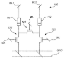
- 磁気抵抗ランダムアクセスメモリ(MRAM)ビットセルにおける読み出しおよび書き込み動作であって、ビットセルは、
第1のビット線に接続された第1の磁気トンネル接合部(MTJ)と、
第2のビット線に接続された第2のMTJと、
前記第1のMTJに接続された第1の端子、ゼロボルトにバイアスされた接地導体に接続された第2の端子、および第3の端子を有する第1のトランジスタと、
前記第2のMTJに接続された第1の端子、前記接地導体に接続された第2の端子、および第3の端子を有する第2のトランジスタと、
前記第1のトランジスタの前記第1の端子に接続された第1の端子、前記第2トランジスタの前記第1の端子に接続された第2の端子、および第3の端子を有する第3のトランジスタと、を含み、
前記第1のトランジスタ、前記第2のトランジスタ、および前記第3のトランジスタの各第3の端子は共通のワード線により制御可能であり、
この読み出し動作は、
前記第1のビット線および前記第2のビット線にそれぞれ読み出し電流を供給し、前記共通のワード線に制御信号を供給して、前記第1のトランジスタを導通モードにして前記第1のMTJと前記接地導体との間に第1の電流を流し、前記第2のトランジスタを導通モードにして前記第2のMTJと前記接地導体との間に第2の電流を流し、前記第3のトランジスタを導通モードにして前記第1のトランジスタの前記第1の端子と前記第2のトランジスタの前記第1の端子との間に第3の電流を流す工程と、
前記第1のビット線と前記第2のビット線との間の電圧差を測定する工程と、を含み、
この書き込み動作は、
前記共通のワード線に制御信号を供給して、前記第1のトランジスタを通電モードにして、前記第1のMTJから前記第1のトランジスタを通って前記接地導体まで第1の電流経路を供給し、前記第3のトランジスタを通電モードにして、前記第1のMTJから前記第3のトランジスタを通って前記第2のMTJまで第2の電流経路を供給し、および前記第2のトランジスタを通電モードにして、前記第1のMTJから前記接地導体まで前記第3のトランジスタおよび前記第2のトランジスタを通って第3の電流経路を供給する工程と、
第1のビット線に書き込み電流を供給し、前記接地導体はゼロボルトのままで、前記第1のMTJと前記第2のMTJとの双方を切り替える工程と、を含み、
前記書き込み電流が前記第1のMTJを通った後に、前記第1の電流経路と前記第3の電流経路の電気抵抗がバランスし、前記第1のビット線からの前記書き込み電流の一部は、前記第2の電流経路に沿って、前記第2のMTJを通って、前記第2のビット線に供給され、前記第2のMTJを切り替える、
読み出しおよび書き込み動作。 - さらに、前記読み出し動作中に、前記第1のビット線と前記第2のビット線との間の電圧差を測定することにより、前記第1のMTJおよび前記第2のMTJのそれぞれの抵抗状態を決定する工程を含む請求項1に記載の読み出しおよび書き込み動作。
- 前記MRAMビットセルは、スピントランスファトルク(STT)MRAMを含む請求項1に記載の読み出しおよび書き込み動作。
- 前記第1、第2、および第3のトランジスタのそれぞれは、読み出し動作および書き込み動作の間に制御可能である請求項1に記載の読み出しおよび書き込み動作。
- 前記接地導体は、接地グリッドを含む請求項1に記載の読み出しおよび書き込み動作。
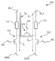
- 磁気抵抗ランダムアクセスメモリ(MRAM)ビットセルにおける書き込み動作であって、ビットセルは、
第1のビット線に接続された第1の磁気トンネル接合部(MTJ)と、
第2のビット線に接続された第2のMTJと、
前記第1のMTJに接続された第1の端子、接地導体に接続された第2の端子、および第3の端子を有する第1のトランジスタと、
前記第2のMTJに接続された第1の端子、前記接地導体に接続された第2の端子、および第3の端子を有する第2のトランジスタと、
前記第1のトランジスタの前記第1の端子に接続された第1の端子、前記第2トランジスタの前記第1の端子に接続された第2の端子、および第3の端子を有する第3のトランジスタと、を含み、
前記第1のトランジスタ、前記第2のトランジスタ、および前記第3のトランジスタの各第3の端子は共通のワード線により制御可能であり、
この書き込み動作は、
前記共通のワード線に制御信号を供給して、前記第1のトランジスタを通電モードにして、前記第1のMTJから前記第1のトランジスタを通って前記接地導体まで第1の電流経路を供給し、前記第3のトランジスタを通電モードにして、前記第1のMTJから前記第3のトランジスタを通って前記第2のMTJまで第2の電流経路を供給し、および前記第2のトランジスタを通電モードにして、前記第1のMTJから前記接地導体まで前記第3のトランジスタおよび前記第2のトランジスタを通って第3の電流経路を供給する工程と、
第1のビット線に書き込み電流を供給し、前記接地導体はゼロボルトのままで、前記第1のMTJと前記第2のMTJとの双方を切り替える工程と、を含み、
前記書き込み電流が前記第1のMTJを通った後に、前記第1の電流経路と前記第3の電流経路の電気抵抗がバランスし、前記第1のビット線からの前記書き込み電流の一部は、前記第2の電流経路に沿って、前記第2のMTJを通って、前記第2のビット線に供給され、前記第2のMTJを切り替える、
書き込み動作。 - 前記第1のMTJおよび前記第2のMTJは、相補型MTJであり、
前記第1のMTJは並列状態であり、前記第2のMTJが逆並列状態である請求項6に記載の書き込み動作。 - 前記第1のMTJは、並列状態から逆並列状態にスイッチングされ、前記第2のMTJは、逆並列状態から並列状態にスイッチングされる請求項6に記載の書き込み動作。
Applications Claiming Priority (2)
| Application Number | Priority Date | Filing Date | Title |
|---|---|---|---|
| EP15198573 | 2015-12-09 | ||
| EP15198573.6 | 2015-12-09 |
Publications (3)
| Publication Number | Publication Date |
|---|---|
| JP2017152071A JP2017152071A (ja) | 2017-08-31 |
| JP2017152071A5 JP2017152071A5 (ja) | 2019-12-12 |
| JP6657063B2 true JP6657063B2 (ja) | 2020-03-04 |
Family
ID=54838247
Family Applications (1)
| Application Number | Title | Priority Date | Filing Date |
|---|---|---|---|
| JP2016238559A Active JP6657063B2 (ja) | 2015-12-09 | 2016-12-08 | 3トランジスタ2接合mramビットセル |
Country Status (2)
| Country | Link |
|---|---|
| US (1) | US10127961B2 (ja) |
| JP (1) | JP6657063B2 (ja) |
Families Citing this family (7)
| Publication number | Priority date | Publication date | Assignee | Title |
|---|---|---|---|---|
| JP6421309B2 (ja) * | 2013-09-30 | 2018-11-14 | テンパール工業株式会社 | 端子台 |
| EP3435413A1 (en) * | 2017-07-28 | 2019-01-30 | IMEC vzw | A semiconductor device and a method for forming a semiconductor device |
| US11290110B2 (en) * | 2017-10-26 | 2022-03-29 | Samsung Electronics Co., Ltd. | Method and system for providing a variation resistant magnetic junction-based XNOR cell usable in neuromorphic computing |
| US10461751B2 (en) | 2018-03-08 | 2019-10-29 | Samsung Electronics Co., Ltd. | FE-FET-based XNOR cell usable in neuromorphic computing |
| US10726896B1 (en) | 2019-01-30 | 2020-07-28 | Globalfoundries Inc. | Resistive nonvolatile memory structure employing a statistical sensing scheme and method |
| CN112542189A (zh) * | 2019-09-20 | 2021-03-23 | 中芯国际集成电路制造(上海)有限公司 | 磁性存储器及其编程控制方法、读取方法、磁性存储装置 |
| US11101320B2 (en) | 2019-10-22 | 2021-08-24 | Samsung Electronics Co., Ltd | System and method for efficient enhancement of an on/off ratio of a bitcell based on 3T2R binary weight cell with spin orbit torque MJTs (SOT-MTJs) |
Family Cites Families (4)
| Publication number | Priority date | Publication date | Assignee | Title |
|---|---|---|---|---|
| US7272034B1 (en) * | 2005-08-31 | 2007-09-18 | Grandis, Inc. | Current driven switching of magnetic storage cells utilizing spin transfer and magnetic memories using such cells |
| US7742329B2 (en) * | 2007-03-06 | 2010-06-22 | Qualcomm Incorporated | Word line transistor strength control for read and write in spin transfer torque magnetoresistive random access memory |
| US8995180B2 (en) * | 2012-11-29 | 2015-03-31 | Taiwan Semiconductor Manufacturing Company, Ltd. | Magnetoresistive random access memory (MRAM) differential bit cell and method of use |
| US9218877B2 (en) * | 2013-06-19 | 2015-12-22 | Broadcom Corporation | Differential bit cell |
-
2016
- 2016-12-02 US US15/367,293 patent/US10127961B2/en active Active
- 2016-12-08 JP JP2016238559A patent/JP6657063B2/ja active Active
Also Published As
| Publication number | Publication date |
|---|---|
| US10127961B2 (en) | 2018-11-13 |
| US20170169873A1 (en) | 2017-06-15 |
| JP2017152071A (ja) | 2017-08-31 |
Similar Documents
| Publication | Publication Date | Title |
|---|---|---|
| JP6657063B2 (ja) | 3トランジスタ2接合mramビットセル | |
| TWI503820B (zh) | 數位記憶體裝置以及磁阻式隨機存取記憶體之配置方法 | |
| US9508923B2 (en) | Magnetic memory using spin orbit interaction | |
| US20190334080A1 (en) | Memory cell, memory array, method of forming and operating memory cell | |
| US9721632B2 (en) | Redundant magnetic tunnel junctions in magnetoresistive memory | |
| TWI550925B (zh) | 數位記憶體、改良磁阻隨機存取記憶體配置以及配置自旋轉移力矩磁阻隨機存取記憶體的方法 | |
| US7894248B2 (en) | Programmable and redundant circuitry based on magnetic tunnel junction (MTJ) | |
| EP2320425B1 (en) | Selection device for a spin transfer torque magnetoresistive random access memory | |
| US7457149B2 (en) | Methods and apparatus for thermally assisted programming of a magnetic memory device | |
| JP2005116162A (ja) | 直列に接続されたメモリ素子のグループを含む磁気メモリデバイス | |
| US11004490B2 (en) | Spin orbit torque magnetoresistive random access memory device | |
| JP2007518216A (ja) | 磁気トンネル接合用の分離書込みおよび読出しアクセスアーキテクチャ | |
| US20180061887A1 (en) | Magnetoresistive random access memory (mram) with an interconnect that generates a spin current and a magnetic field effect | |
| US11527709B2 (en) | SOT multibit memory cell | |
| US7986548B2 (en) | Current re-routing scheme for serial-programmed MRAM | |
| EP3945521A1 (en) | Magnetic random access memory cell and method for reading said cell | |
| JP5147972B2 (ja) | 薄膜磁性体記憶装置 |
Legal Events
| Date | Code | Title | Description |
|---|---|---|---|
| A521 | Request for written amendment filed |
Free format text: JAPANESE INTERMEDIATE CODE: A523 Effective date: 20191030 |
|
| A621 | Written request for application examination |
Free format text: JAPANESE INTERMEDIATE CODE: A621 Effective date: 20191030 |
|
| A871 | Explanation of circumstances concerning accelerated examination |
Free format text: JAPANESE INTERMEDIATE CODE: A871 Effective date: 20191030 |
|
| A975 | Report on accelerated examination |
Free format text: JAPANESE INTERMEDIATE CODE: A971005 Effective date: 20191031 |
|
| TRDD | Decision of grant or rejection written | ||
| A01 | Written decision to grant a patent or to grant a registration (utility model) |
Free format text: JAPANESE INTERMEDIATE CODE: A01 Effective date: 20200107 |
|
| A61 | First payment of annual fees (during grant procedure) |
Free format text: JAPANESE INTERMEDIATE CODE: A61 Effective date: 20200205 |
|
| R150 | Certificate of patent or registration of utility model |
Ref document number: 6657063 Country of ref document: JP Free format text: JAPANESE INTERMEDIATE CODE: R150 |
|
| R250 | Receipt of annual fees |
Free format text: JAPANESE INTERMEDIATE CODE: R250 |
|
| R250 | Receipt of annual fees |
Free format text: JAPANESE INTERMEDIATE CODE: R250 |