JP6643382B2 - Power semiconductor device - Google Patents
Power semiconductor device Download PDFInfo
- Publication number
- JP6643382B2 JP6643382B2 JP2018051006A JP2018051006A JP6643382B2 JP 6643382 B2 JP6643382 B2 JP 6643382B2 JP 2018051006 A JP2018051006 A JP 2018051006A JP 2018051006 A JP2018051006 A JP 2018051006A JP 6643382 B2 JP6643382 B2 JP 6643382B2
- Authority
- JP
- Japan
- Prior art keywords
- region
- power semiconductor
- recombination
- semiconductor device
- doped
- Prior art date
- Legal status (The legal status is an assumption and is not a legal conclusion. Google has not performed a legal analysis and makes no representation as to the accuracy of the status listed.)
- Active
Links
- 239000004065 semiconductor Substances 0.000 title claims description 393
- 230000006798 recombination Effects 0.000 claims description 188
- 238000005215 recombination Methods 0.000 claims description 187
- 239000002019 doping agent Substances 0.000 claims description 170
- 230000004888 barrier function Effects 0.000 claims description 107
- 230000000903 blocking effect Effects 0.000 claims description 79
- 230000007547 defect Effects 0.000 claims description 57
- 239000013078 crystal Substances 0.000 claims description 56
- 230000002441 reversible effect Effects 0.000 claims description 44
- 239000002800 charge carrier Substances 0.000 claims description 18
- 230000007704 transition Effects 0.000 claims description 13
- 238000009413 insulation Methods 0.000 claims description 7
- 238000000034 method Methods 0.000 description 46
- 210000000746 body region Anatomy 0.000 description 24
- 108091006146 Channels Proteins 0.000 description 23
- 238000002513 implantation Methods 0.000 description 20
- 239000000463 material Substances 0.000 description 20
- 230000005684 electric field Effects 0.000 description 19
- BASFCYQUMIYNBI-UHFFFAOYSA-N platinum Chemical group [Pt] BASFCYQUMIYNBI-UHFFFAOYSA-N 0.000 description 12
- 229910002601 GaN Inorganic materials 0.000 description 11
- 235000012431 wafers Nutrition 0.000 description 9
- XKRFYHLGVUSROY-UHFFFAOYSA-N Argon Chemical compound [Ar] XKRFYHLGVUSROY-UHFFFAOYSA-N 0.000 description 8
- 230000015556 catabolic process Effects 0.000 description 8
- 230000006870 function Effects 0.000 description 8
- 150000002500 ions Chemical class 0.000 description 8
- JMASRVWKEDWRBT-UHFFFAOYSA-N Gallium nitride Chemical compound [Ga]#N JMASRVWKEDWRBT-UHFFFAOYSA-N 0.000 description 7
- ZOKXTWBITQBERF-UHFFFAOYSA-N Molybdenum Chemical compound [Mo] ZOKXTWBITQBERF-UHFFFAOYSA-N 0.000 description 6
- XUIMIQQOPSSXEZ-UHFFFAOYSA-N Silicon Chemical compound [Si] XUIMIQQOPSSXEZ-UHFFFAOYSA-N 0.000 description 6
- 238000000137 annealing Methods 0.000 description 6
- 238000009792 diffusion process Methods 0.000 description 6
- 239000007943 implant Substances 0.000 description 6
- 229910052750 molybdenum Inorganic materials 0.000 description 6
- 239000011733 molybdenum Substances 0.000 description 6
- 229910052710 silicon Inorganic materials 0.000 description 6
- 239000010703 silicon Substances 0.000 description 6
- KDLHZDBZIXYQEI-UHFFFAOYSA-N Palladium Chemical compound [Pd] KDLHZDBZIXYQEI-UHFFFAOYSA-N 0.000 description 5
- 230000001413 cellular effect Effects 0.000 description 5
- 230000008859 change Effects 0.000 description 5
- 230000007423 decrease Effects 0.000 description 5
- 229910052738 indium Inorganic materials 0.000 description 5
- APFVFJFRJDLVQX-UHFFFAOYSA-N indium atom Chemical compound [In] APFVFJFRJDLVQX-UHFFFAOYSA-N 0.000 description 5
- 238000001465 metallisation Methods 0.000 description 5
- 229910052697 platinum Inorganic materials 0.000 description 5
- 230000008569 process Effects 0.000 description 5
- 230000001052 transient effect Effects 0.000 description 5
- ZOXJGFHDIHLPTG-UHFFFAOYSA-N Boron Chemical compound [B] ZOXJGFHDIHLPTG-UHFFFAOYSA-N 0.000 description 4
- RNQKDQAVIXDKAG-UHFFFAOYSA-N aluminum gallium Chemical compound [Al].[Ga] RNQKDQAVIXDKAG-UHFFFAOYSA-N 0.000 description 4
- 229910052786 argon Inorganic materials 0.000 description 4
- QVGXLLKOCUKJST-UHFFFAOYSA-N atomic oxygen Chemical compound [O] QVGXLLKOCUKJST-UHFFFAOYSA-N 0.000 description 4
- 229910052796 boron Inorganic materials 0.000 description 4
- 230000001747 exhibiting effect Effects 0.000 description 4
- PCHJSUWPFVWCPO-UHFFFAOYSA-N gold Chemical group [Au] PCHJSUWPFVWCPO-UHFFFAOYSA-N 0.000 description 4
- 229910052734 helium Inorganic materials 0.000 description 4
- 239000001307 helium Substances 0.000 description 4
- SWQJXJOGLNCZEY-UHFFFAOYSA-N helium atom Chemical compound [He] SWQJXJOGLNCZEY-UHFFFAOYSA-N 0.000 description 4
- 238000002347 injection Methods 0.000 description 4
- 239000007924 injection Substances 0.000 description 4
- 229910052760 oxygen Inorganic materials 0.000 description 4
- 239000001301 oxygen Substances 0.000 description 4
- 229910000577 Silicon-germanium Inorganic materials 0.000 description 3
- NWAIGJYBQQYSPW-UHFFFAOYSA-N azanylidyneindigane Chemical compound [In]#N NWAIGJYBQQYSPW-UHFFFAOYSA-N 0.000 description 3
- 238000010586 diagram Methods 0.000 description 3
- 229910052737 gold Inorganic materials 0.000 description 3
- 239000010931 gold Substances 0.000 description 3
- 239000012212 insulator Substances 0.000 description 3
- 238000003672 processing method Methods 0.000 description 3
- MARUHZGHZWCEQU-UHFFFAOYSA-N 5-phenyl-2h-tetrazole Chemical compound C1=CC=CC=C1C1=NNN=N1 MARUHZGHZWCEQU-UHFFFAOYSA-N 0.000 description 2
- JBRZTFJDHDCESZ-UHFFFAOYSA-N AsGa Chemical compound [As]#[Ga] JBRZTFJDHDCESZ-UHFFFAOYSA-N 0.000 description 2
- HZXMRANICFIONG-UHFFFAOYSA-N gallium phosphide Chemical compound [Ga]#P HZXMRANICFIONG-UHFFFAOYSA-N 0.000 description 2
- 229910001385 heavy metal Inorganic materials 0.000 description 2
- 238000005468 ion implantation Methods 0.000 description 2
- 238000004519 manufacturing process Methods 0.000 description 2
- 229910052763 palladium Inorganic materials 0.000 description 2
- HBMJWWWQQXIZIP-UHFFFAOYSA-N silicon carbide Chemical compound [Si+]#[C-] HBMJWWWQQXIZIP-UHFFFAOYSA-N 0.000 description 2
- 229910010271 silicon carbide Inorganic materials 0.000 description 2
- 229910052720 vanadium Inorganic materials 0.000 description 2
- 101100207343 Antirrhinum majus 1e20 gene Proteins 0.000 description 1
- 229910005540 GaP Inorganic materials 0.000 description 1
- 229910001218 Gallium arsenide Inorganic materials 0.000 description 1
- 229910000530 Gallium indium arsenide Inorganic materials 0.000 description 1
- GPXJNWSHGFTCBW-UHFFFAOYSA-N Indium phosphide Chemical compound [In]#P GPXJNWSHGFTCBW-UHFFFAOYSA-N 0.000 description 1
- 229910000661 Mercury cadmium telluride Inorganic materials 0.000 description 1
- KXNLCSXBJCPWGL-UHFFFAOYSA-N [Ga].[As].[In] Chemical compound [Ga].[As].[In] KXNLCSXBJCPWGL-UHFFFAOYSA-N 0.000 description 1
- LEVVHYCKPQWKOP-UHFFFAOYSA-N [Si].[Ge] Chemical compound [Si].[Ge] LEVVHYCKPQWKOP-UHFFFAOYSA-N 0.000 description 1
- 230000009471 action Effects 0.000 description 1
- AJGDITRVXRPLBY-UHFFFAOYSA-N aluminum indium Chemical compound [Al].[In] AJGDITRVXRPLBY-UHFFFAOYSA-N 0.000 description 1
- 229910021417 amorphous silicon Inorganic materials 0.000 description 1
- 230000003321 amplification Effects 0.000 description 1
- 230000008901 benefit Effects 0.000 description 1
- DGJPPCSCQOIWCP-UHFFFAOYSA-N cadmium mercury Chemical compound [Cd].[Hg] DGJPPCSCQOIWCP-UHFFFAOYSA-N 0.000 description 1
- 239000003990 capacitor Substances 0.000 description 1
- 238000006243 chemical reaction Methods 0.000 description 1
- 239000002131 composite material Substances 0.000 description 1
- 150000001875 compounds Chemical class 0.000 description 1
- 230000003750 conditioning effect Effects 0.000 description 1
- 239000004020 conductor Substances 0.000 description 1
- 238000013500 data storage Methods 0.000 description 1
- 238000000151 deposition Methods 0.000 description 1
- 230000000694 effects Effects 0.000 description 1
- 238000010292 electrical insulation Methods 0.000 description 1
- 230000005669 field effect Effects 0.000 description 1
- 229910052732 germanium Inorganic materials 0.000 description 1
- GNPVGFCGXDBREM-UHFFFAOYSA-N germanium atom Chemical compound [Ge] GNPVGFCGXDBREM-UHFFFAOYSA-N 0.000 description 1
- 230000006698 induction Effects 0.000 description 1
- 238000002955 isolation Methods 0.000 description 1
- 239000011159 matrix material Substances 0.000 description 1
- 229910044991 metal oxide Inorganic materials 0.000 description 1
- 150000004706 metal oxides Chemical class 0.000 description 1
- 230000004048 modification Effects 0.000 description 1
- 238000012986 modification Methods 0.000 description 1
- 229910021421 monocrystalline silicon Inorganic materials 0.000 description 1
- 238000003199 nucleic acid amplification method Methods 0.000 description 1
- 150000002926 oxygen Chemical class 0.000 description 1
- 229910021420 polycrystalline silicon Inorganic materials 0.000 description 1
- 230000009467 reduction Effects 0.000 description 1
- SBEQWOXEGHQIMW-UHFFFAOYSA-N silicon Chemical compound [Si].[Si] SBEQWOXEGHQIMW-UHFFFAOYSA-N 0.000 description 1
- 230000007480 spreading Effects 0.000 description 1
- 238000003892 spreading Methods 0.000 description 1
- 239000000758 substrate Substances 0.000 description 1
- 229910052727 yttrium Inorganic materials 0.000 description 1
Images


Classifications
-
- H—ELECTRICITY
- H01—ELECTRIC ELEMENTS
- H01L—SEMICONDUCTOR DEVICES NOT COVERED BY CLASS H10
- H01L29/00—Semiconductor devices adapted for rectifying, amplifying, oscillating or switching, or capacitors or resistors with at least one potential-jump barrier or surface barrier, e.g. PN junction depletion layer or carrier concentration layer; Details of semiconductor bodies or of electrodes thereof ; Multistep manufacturing processes therefor
- H01L29/66—Types of semiconductor device ; Multistep manufacturing processes therefor
- H01L29/68—Types of semiconductor device ; Multistep manufacturing processes therefor controllable by only the electric current supplied, or only the electric potential applied, to an electrode which does not carry the current to be rectified, amplified or switched
- H01L29/70—Bipolar devices
- H01L29/72—Transistor-type devices, i.e. able to continuously respond to applied control signals
- H01L29/739—Transistor-type devices, i.e. able to continuously respond to applied control signals controlled by field-effect, e.g. bipolar static induction transistors [BSIT]
- H01L29/7393—Insulated gate bipolar mode transistors, i.e. IGBT; IGT; COMFET
- H01L29/7395—Vertical transistors, e.g. vertical IGBT
-
- H—ELECTRICITY
- H01—ELECTRIC ELEMENTS
- H01L—SEMICONDUCTOR DEVICES NOT COVERED BY CLASS H10
- H01L23/00—Details of semiconductor or other solid state devices
- H01L23/58—Structural electrical arrangements for semiconductor devices not otherwise provided for, e.g. in combination with batteries
- H01L23/62—Protection against overvoltage, e.g. fuses, shunts
-
- H—ELECTRICITY
- H01—ELECTRIC ELEMENTS
- H01L—SEMICONDUCTOR DEVICES NOT COVERED BY CLASS H10
- H01L27/00—Devices consisting of a plurality of semiconductor or other solid-state components formed in or on a common substrate
- H01L27/02—Devices consisting of a plurality of semiconductor or other solid-state components formed in or on a common substrate including semiconductor components specially adapted for rectifying, oscillating, amplifying or switching and having at least one potential-jump barrier or surface barrier; including integrated passive circuit elements with at least one potential-jump barrier or surface barrier
- H01L27/0203—Particular design considerations for integrated circuits
- H01L27/0248—Particular design considerations for integrated circuits for electrical or thermal protection, e.g. electrostatic discharge [ESD] protection
- H01L27/0251—Particular design considerations for integrated circuits for electrical or thermal protection, e.g. electrostatic discharge [ESD] protection for MOS devices
- H01L27/0255—Particular design considerations for integrated circuits for electrical or thermal protection, e.g. electrostatic discharge [ESD] protection for MOS devices using diodes as protective elements
-
- H—ELECTRICITY
- H01—ELECTRIC ELEMENTS
- H01L—SEMICONDUCTOR DEVICES NOT COVERED BY CLASS H10
- H01L27/00—Devices consisting of a plurality of semiconductor or other solid-state components formed in or on a common substrate
- H01L27/02—Devices consisting of a plurality of semiconductor or other solid-state components formed in or on a common substrate including semiconductor components specially adapted for rectifying, oscillating, amplifying or switching and having at least one potential-jump barrier or surface barrier; including integrated passive circuit elements with at least one potential-jump barrier or surface barrier
- H01L27/04—Devices consisting of a plurality of semiconductor or other solid-state components formed in or on a common substrate including semiconductor components specially adapted for rectifying, oscillating, amplifying or switching and having at least one potential-jump barrier or surface barrier; including integrated passive circuit elements with at least one potential-jump barrier or surface barrier the substrate being a semiconductor body
- H01L27/06—Devices consisting of a plurality of semiconductor or other solid-state components formed in or on a common substrate including semiconductor components specially adapted for rectifying, oscillating, amplifying or switching and having at least one potential-jump barrier or surface barrier; including integrated passive circuit elements with at least one potential-jump barrier or surface barrier the substrate being a semiconductor body including a plurality of individual components in a non-repetitive configuration
- H01L27/07—Devices consisting of a plurality of semiconductor or other solid-state components formed in or on a common substrate including semiconductor components specially adapted for rectifying, oscillating, amplifying or switching and having at least one potential-jump barrier or surface barrier; including integrated passive circuit elements with at least one potential-jump barrier or surface barrier the substrate being a semiconductor body including a plurality of individual components in a non-repetitive configuration the components having an active region in common
- H01L27/0705—Devices consisting of a plurality of semiconductor or other solid-state components formed in or on a common substrate including semiconductor components specially adapted for rectifying, oscillating, amplifying or switching and having at least one potential-jump barrier or surface barrier; including integrated passive circuit elements with at least one potential-jump barrier or surface barrier the substrate being a semiconductor body including a plurality of individual components in a non-repetitive configuration the components having an active region in common comprising components of the field effect type
- H01L27/0727—Devices consisting of a plurality of semiconductor or other solid-state components formed in or on a common substrate including semiconductor components specially adapted for rectifying, oscillating, amplifying or switching and having at least one potential-jump barrier or surface barrier; including integrated passive circuit elements with at least one potential-jump barrier or surface barrier the substrate being a semiconductor body including a plurality of individual components in a non-repetitive configuration the components having an active region in common comprising components of the field effect type in combination with diodes, or capacitors or resistors
-
- H—ELECTRICITY
- H01—ELECTRIC ELEMENTS
- H01L—SEMICONDUCTOR DEVICES NOT COVERED BY CLASS H10
- H01L29/00—Semiconductor devices adapted for rectifying, amplifying, oscillating or switching, or capacitors or resistors with at least one potential-jump barrier or surface barrier, e.g. PN junction depletion layer or carrier concentration layer; Details of semiconductor bodies or of electrodes thereof ; Multistep manufacturing processes therefor
- H01L29/02—Semiconductor bodies ; Multistep manufacturing processes therefor
- H01L29/04—Semiconductor bodies ; Multistep manufacturing processes therefor characterised by their crystalline structure, e.g. polycrystalline, cubic or particular orientation of crystalline planes
-
- H—ELECTRICITY
- H01—ELECTRIC ELEMENTS
- H01L—SEMICONDUCTOR DEVICES NOT COVERED BY CLASS H10
- H01L29/00—Semiconductor devices adapted for rectifying, amplifying, oscillating or switching, or capacitors or resistors with at least one potential-jump barrier or surface barrier, e.g. PN junction depletion layer or carrier concentration layer; Details of semiconductor bodies or of electrodes thereof ; Multistep manufacturing processes therefor
- H01L29/02—Semiconductor bodies ; Multistep manufacturing processes therefor
- H01L29/06—Semiconductor bodies ; Multistep manufacturing processes therefor characterised by their shape; characterised by the shapes, relative sizes, or dispositions of the semiconductor regions ; characterised by the concentration or distribution of impurities within semiconductor regions
- H01L29/0684—Semiconductor bodies ; Multistep manufacturing processes therefor characterised by their shape; characterised by the shapes, relative sizes, or dispositions of the semiconductor regions ; characterised by the concentration or distribution of impurities within semiconductor regions characterised by the shape, relative sizes or dispositions of the semiconductor regions or junctions between the regions
-
- H—ELECTRICITY
- H01—ELECTRIC ELEMENTS
- H01L—SEMICONDUCTOR DEVICES NOT COVERED BY CLASS H10
- H01L29/00—Semiconductor devices adapted for rectifying, amplifying, oscillating or switching, or capacitors or resistors with at least one potential-jump barrier or surface barrier, e.g. PN junction depletion layer or carrier concentration layer; Details of semiconductor bodies or of electrodes thereof ; Multistep manufacturing processes therefor
- H01L29/02—Semiconductor bodies ; Multistep manufacturing processes therefor
- H01L29/06—Semiconductor bodies ; Multistep manufacturing processes therefor characterised by their shape; characterised by the shapes, relative sizes, or dispositions of the semiconductor regions ; characterised by the concentration or distribution of impurities within semiconductor regions
- H01L29/08—Semiconductor bodies ; Multistep manufacturing processes therefor characterised by their shape; characterised by the shapes, relative sizes, or dispositions of the semiconductor regions ; characterised by the concentration or distribution of impurities within semiconductor regions with semiconductor regions connected to an electrode carrying current to be rectified, amplified or switched and such electrode being part of a semiconductor device which comprises three or more electrodes
- H01L29/083—Anode or cathode regions of thyristors or gated bipolar-mode devices
-
- H—ELECTRICITY
- H01—ELECTRIC ELEMENTS
- H01L—SEMICONDUCTOR DEVICES NOT COVERED BY CLASS H10
- H01L29/00—Semiconductor devices adapted for rectifying, amplifying, oscillating or switching, or capacitors or resistors with at least one potential-jump barrier or surface barrier, e.g. PN junction depletion layer or carrier concentration layer; Details of semiconductor bodies or of electrodes thereof ; Multistep manufacturing processes therefor
- H01L29/02—Semiconductor bodies ; Multistep manufacturing processes therefor
- H01L29/06—Semiconductor bodies ; Multistep manufacturing processes therefor characterised by their shape; characterised by the shapes, relative sizes, or dispositions of the semiconductor regions ; characterised by the concentration or distribution of impurities within semiconductor regions
- H01L29/10—Semiconductor bodies ; Multistep manufacturing processes therefor characterised by their shape; characterised by the shapes, relative sizes, or dispositions of the semiconductor regions ; characterised by the concentration or distribution of impurities within semiconductor regions with semiconductor regions connected to an electrode not carrying current to be rectified, amplified or switched and such electrode being part of a semiconductor device which comprises three or more electrodes
- H01L29/1095—Body region, i.e. base region, of DMOS transistors or IGBTs
-
- H—ELECTRICITY
- H01—ELECTRIC ELEMENTS
- H01L—SEMICONDUCTOR DEVICES NOT COVERED BY CLASS H10
- H01L29/00—Semiconductor devices adapted for rectifying, amplifying, oscillating or switching, or capacitors or resistors with at least one potential-jump barrier or surface barrier, e.g. PN junction depletion layer or carrier concentration layer; Details of semiconductor bodies or of electrodes thereof ; Multistep manufacturing processes therefor
- H01L29/02—Semiconductor bodies ; Multistep manufacturing processes therefor
- H01L29/30—Semiconductor bodies ; Multistep manufacturing processes therefor characterised by physical imperfections; having polished or roughened surface
- H01L29/32—Semiconductor bodies ; Multistep manufacturing processes therefor characterised by physical imperfections; having polished or roughened surface the imperfections being within the semiconductor body
-
- H—ELECTRICITY
- H01—ELECTRIC ELEMENTS
- H01L—SEMICONDUCTOR DEVICES NOT COVERED BY CLASS H10
- H01L29/00—Semiconductor devices adapted for rectifying, amplifying, oscillating or switching, or capacitors or resistors with at least one potential-jump barrier or surface barrier, e.g. PN junction depletion layer or carrier concentration layer; Details of semiconductor bodies or of electrodes thereof ; Multistep manufacturing processes therefor
- H01L29/02—Semiconductor bodies ; Multistep manufacturing processes therefor
- H01L29/36—Semiconductor bodies ; Multistep manufacturing processes therefor characterised by the concentration or distribution of impurities in the bulk material
-
- H—ELECTRICITY
- H01—ELECTRIC ELEMENTS
- H01L—SEMICONDUCTOR DEVICES NOT COVERED BY CLASS H10
- H01L29/00—Semiconductor devices adapted for rectifying, amplifying, oscillating or switching, or capacitors or resistors with at least one potential-jump barrier or surface barrier, e.g. PN junction depletion layer or carrier concentration layer; Details of semiconductor bodies or of electrodes thereof ; Multistep manufacturing processes therefor
- H01L29/40—Electrodes ; Multistep manufacturing processes therefor
- H01L29/41—Electrodes ; Multistep manufacturing processes therefor characterised by their shape, relative sizes or dispositions
- H01L29/423—Electrodes ; Multistep manufacturing processes therefor characterised by their shape, relative sizes or dispositions not carrying the current to be rectified, amplified or switched
-
- H—ELECTRICITY
- H01—ELECTRIC ELEMENTS
- H01L—SEMICONDUCTOR DEVICES NOT COVERED BY CLASS H10
- H01L29/00—Semiconductor devices adapted for rectifying, amplifying, oscillating or switching, or capacitors or resistors with at least one potential-jump barrier or surface barrier, e.g. PN junction depletion layer or carrier concentration layer; Details of semiconductor bodies or of electrodes thereof ; Multistep manufacturing processes therefor
- H01L29/66—Types of semiconductor device ; Multistep manufacturing processes therefor
- H01L29/66007—Multistep manufacturing processes
- H01L29/66075—Multistep manufacturing processes of devices having semiconductor bodies comprising group 14 or group 13/15 materials
- H01L29/66227—Multistep manufacturing processes of devices having semiconductor bodies comprising group 14 or group 13/15 materials the devices being controllable only by the electric current supplied or the electric potential applied, to an electrode which does not carry the current to be rectified, amplified or switched, e.g. three-terminal devices
- H01L29/66234—Bipolar junction transistors [BJT]
- H01L29/66325—Bipolar junction transistors [BJT] controlled by field-effect, e.g. insulated gate bipolar transistors [IGBT]
- H01L29/66333—Vertical insulated gate bipolar transistors
- H01L29/66348—Vertical insulated gate bipolar transistors with a recessed gate
-
- H—ELECTRICITY
- H01—ELECTRIC ELEMENTS
- H01L—SEMICONDUCTOR DEVICES NOT COVERED BY CLASS H10
- H01L29/00—Semiconductor devices adapted for rectifying, amplifying, oscillating or switching, or capacitors or resistors with at least one potential-jump barrier or surface barrier, e.g. PN junction depletion layer or carrier concentration layer; Details of semiconductor bodies or of electrodes thereof ; Multistep manufacturing processes therefor
- H01L29/66—Types of semiconductor device ; Multistep manufacturing processes therefor
- H01L29/68—Types of semiconductor device ; Multistep manufacturing processes therefor controllable by only the electric current supplied, or only the electric potential applied, to an electrode which does not carry the current to be rectified, amplified or switched
- H01L29/70—Bipolar devices
- H01L29/72—Transistor-type devices, i.e. able to continuously respond to applied control signals
- H01L29/739—Transistor-type devices, i.e. able to continuously respond to applied control signals controlled by field-effect, e.g. bipolar static induction transistors [BSIT]
- H01L29/7393—Insulated gate bipolar mode transistors, i.e. IGBT; IGT; COMFET
- H01L29/7395—Vertical transistors, e.g. vertical IGBT
- H01L29/7396—Vertical transistors, e.g. vertical IGBT with a non planar surface, e.g. with a non planar gate or with a trench or recess or pillar in the surface of the emitter, base or collector region for improving current density or short circuiting the emitter and base regions
- H01L29/7397—Vertical transistors, e.g. vertical IGBT with a non planar surface, e.g. with a non planar gate or with a trench or recess or pillar in the surface of the emitter, base or collector region for improving current density or short circuiting the emitter and base regions and a gate structure lying on a slanted or vertical surface or formed in a groove, e.g. trench gate IGBT
-
- H—ELECTRICITY
- H01—ELECTRIC ELEMENTS
- H01L—SEMICONDUCTOR DEVICES NOT COVERED BY CLASS H10
- H01L29/00—Semiconductor devices adapted for rectifying, amplifying, oscillating or switching, or capacitors or resistors with at least one potential-jump barrier or surface barrier, e.g. PN junction depletion layer or carrier concentration layer; Details of semiconductor bodies or of electrodes thereof ; Multistep manufacturing processes therefor
- H01L29/66—Types of semiconductor device ; Multistep manufacturing processes therefor
- H01L29/68—Types of semiconductor device ; Multistep manufacturing processes therefor controllable by only the electric current supplied, or only the electric potential applied, to an electrode which does not carry the current to be rectified, amplified or switched
- H01L29/76—Unipolar devices, e.g. field effect transistors
- H01L29/772—Field effect transistors
- H01L29/80—Field effect transistors with field effect produced by a PN or other rectifying junction gate, i.e. potential-jump barrier
- H01L29/808—Field effect transistors with field effect produced by a PN or other rectifying junction gate, i.e. potential-jump barrier with a PN junction gate, e.g. PN homojunction gate
- H01L29/8083—Vertical transistors
-
- H—ELECTRICITY
- H01—ELECTRIC ELEMENTS
- H01L—SEMICONDUCTOR DEVICES NOT COVERED BY CLASS H10
- H01L29/00—Semiconductor devices adapted for rectifying, amplifying, oscillating or switching, or capacitors or resistors with at least one potential-jump barrier or surface barrier, e.g. PN junction depletion layer or carrier concentration layer; Details of semiconductor bodies or of electrodes thereof ; Multistep manufacturing processes therefor
- H01L29/66—Types of semiconductor device ; Multistep manufacturing processes therefor
- H01L29/86—Types of semiconductor device ; Multistep manufacturing processes therefor controllable only by variation of the electric current supplied, or only the electric potential applied, to one or more of the electrodes carrying the current to be rectified, amplified, oscillated or switched
- H01L29/861—Diodes
-
- H—ELECTRICITY
- H01—ELECTRIC ELEMENTS
- H01L—SEMICONDUCTOR DEVICES NOT COVERED BY CLASS H10
- H01L2224/00—Indexing scheme for arrangements for connecting or disconnecting semiconductor or solid-state bodies and methods related thereto as covered by H01L24/00
- H01L2224/01—Means for bonding being attached to, or being formed on, the surface to be connected, e.g. chip-to-package, die-attach, "first-level" interconnects; Manufacturing methods related thereto
- H01L2224/02—Bonding areas; Manufacturing methods related thereto
- H01L2224/04—Structure, shape, material or disposition of the bonding areas prior to the connecting process
- H01L2224/06—Structure, shape, material or disposition of the bonding areas prior to the connecting process of a plurality of bonding areas
- H01L2224/0601—Structure
- H01L2224/0603—Bonding areas having different sizes, e.g. different heights or widths
-
- H—ELECTRICITY
- H01—ELECTRIC ELEMENTS
- H01L—SEMICONDUCTOR DEVICES NOT COVERED BY CLASS H10
- H01L2224/00—Indexing scheme for arrangements for connecting or disconnecting semiconductor or solid-state bodies and methods related thereto as covered by H01L24/00
- H01L2224/01—Means for bonding being attached to, or being formed on, the surface to be connected, e.g. chip-to-package, die-attach, "first-level" interconnects; Manufacturing methods related thereto
- H01L2224/42—Wire connectors; Manufacturing methods related thereto
- H01L2224/47—Structure, shape, material or disposition of the wire connectors after the connecting process
- H01L2224/49—Structure, shape, material or disposition of the wire connectors after the connecting process of a plurality of wire connectors
- H01L2224/491—Disposition
- H01L2224/4911—Disposition the connectors being bonded to at least one common bonding area, e.g. daisy chain
- H01L2224/49113—Disposition the connectors being bonded to at least one common bonding area, e.g. daisy chain the connectors connecting different bonding areas on the semiconductor or solid-state body to a common bonding area outside the body, e.g. converging wires
-
- H—ELECTRICITY
- H01—ELECTRIC ELEMENTS
- H01L—SEMICONDUCTOR DEVICES NOT COVERED BY CLASS H10
- H01L29/00—Semiconductor devices adapted for rectifying, amplifying, oscillating or switching, or capacitors or resistors with at least one potential-jump barrier or surface barrier, e.g. PN junction depletion layer or carrier concentration layer; Details of semiconductor bodies or of electrodes thereof ; Multistep manufacturing processes therefor
- H01L29/02—Semiconductor bodies ; Multistep manufacturing processes therefor
- H01L29/06—Semiconductor bodies ; Multistep manufacturing processes therefor characterised by their shape; characterised by the shapes, relative sizes, or dispositions of the semiconductor regions ; characterised by the concentration or distribution of impurities within semiconductor regions
- H01L29/08—Semiconductor bodies ; Multistep manufacturing processes therefor characterised by their shape; characterised by the shapes, relative sizes, or dispositions of the semiconductor regions ; characterised by the concentration or distribution of impurities within semiconductor regions with semiconductor regions connected to an electrode carrying current to be rectified, amplified or switched and such electrode being part of a semiconductor device which comprises three or more electrodes
- H01L29/083—Anode or cathode regions of thyristors or gated bipolar-mode devices
- H01L29/0834—Anode regions of thyristors or gated bipolar-mode devices, e.g. supplementary regions surrounding anode regions
-
- H—ELECTRICITY
- H01—ELECTRIC ELEMENTS
- H01L—SEMICONDUCTOR DEVICES NOT COVERED BY CLASS H10
- H01L29/00—Semiconductor devices adapted for rectifying, amplifying, oscillating or switching, or capacitors or resistors with at least one potential-jump barrier or surface barrier, e.g. PN junction depletion layer or carrier concentration layer; Details of semiconductor bodies or of electrodes thereof ; Multistep manufacturing processes therefor
- H01L29/02—Semiconductor bodies ; Multistep manufacturing processes therefor
- H01L29/12—Semiconductor bodies ; Multistep manufacturing processes therefor characterised by the materials of which they are formed
- H01L29/16—Semiconductor bodies ; Multistep manufacturing processes therefor characterised by the materials of which they are formed including, apart from doping materials or other impurities, only elements of Group IV of the Periodic System
-
- H—ELECTRICITY
- H01—ELECTRIC ELEMENTS
- H01L—SEMICONDUCTOR DEVICES NOT COVERED BY CLASS H10
- H01L29/00—Semiconductor devices adapted for rectifying, amplifying, oscillating or switching, or capacitors or resistors with at least one potential-jump barrier or surface barrier, e.g. PN junction depletion layer or carrier concentration layer; Details of semiconductor bodies or of electrodes thereof ; Multistep manufacturing processes therefor
- H01L29/66—Types of semiconductor device ; Multistep manufacturing processes therefor
- H01L29/66007—Multistep manufacturing processes
- H01L29/66075—Multistep manufacturing processes of devices having semiconductor bodies comprising group 14 or group 13/15 materials
- H01L29/66227—Multistep manufacturing processes of devices having semiconductor bodies comprising group 14 or group 13/15 materials the devices being controllable only by the electric current supplied or the electric potential applied, to an electrode which does not carry the current to be rectified, amplified or switched, e.g. three-terminal devices
- H01L29/66234—Bipolar junction transistors [BJT]
- H01L29/66325—Bipolar junction transistors [BJT] controlled by field-effect, e.g. insulated gate bipolar transistors [IGBT]
-
- H—ELECTRICITY
- H01—ELECTRIC ELEMENTS
- H01L—SEMICONDUCTOR DEVICES NOT COVERED BY CLASS H10
- H01L29/00—Semiconductor devices adapted for rectifying, amplifying, oscillating or switching, or capacitors or resistors with at least one potential-jump barrier or surface barrier, e.g. PN junction depletion layer or carrier concentration layer; Details of semiconductor bodies or of electrodes thereof ; Multistep manufacturing processes therefor
- H01L29/66—Types of semiconductor device ; Multistep manufacturing processes therefor
- H01L29/68—Types of semiconductor device ; Multistep manufacturing processes therefor controllable by only the electric current supplied, or only the electric potential applied, to an electrode which does not carry the current to be rectified, amplified or switched
- H01L29/70—Bipolar devices
- H01L29/72—Transistor-type devices, i.e. able to continuously respond to applied control signals
- H01L29/739—Transistor-type devices, i.e. able to continuously respond to applied control signals controlled by field-effect, e.g. bipolar static induction transistors [BSIT]
- H01L29/7393—Insulated gate bipolar mode transistors, i.e. IGBT; IGT; COMFET
- H01L29/7395—Vertical transistors, e.g. vertical IGBT
- H01L29/7398—Vertical transistors, e.g. vertical IGBT with both emitter and collector contacts in the same substrate side
-
- H—ELECTRICITY
- H01—ELECTRIC ELEMENTS
- H01L—SEMICONDUCTOR DEVICES NOT COVERED BY CLASS H10
- H01L29/00—Semiconductor devices adapted for rectifying, amplifying, oscillating or switching, or capacitors or resistors with at least one potential-jump barrier or surface barrier, e.g. PN junction depletion layer or carrier concentration layer; Details of semiconductor bodies or of electrodes thereof ; Multistep manufacturing processes therefor
- H01L29/66—Types of semiconductor device ; Multistep manufacturing processes therefor
- H01L29/68—Types of semiconductor device ; Multistep manufacturing processes therefor controllable by only the electric current supplied, or only the electric potential applied, to an electrode which does not carry the current to be rectified, amplified or switched
- H01L29/70—Bipolar devices
- H01L29/74—Thyristor-type devices, e.g. having four-zone regenerative action
- H01L29/7428—Thyristor-type devices, e.g. having four-zone regenerative action having an amplifying gate structure, e.g. cascade (Darlington) configuration
-
- H—ELECTRICITY
- H01—ELECTRIC ELEMENTS
- H01L—SEMICONDUCTOR DEVICES NOT COVERED BY CLASS H10
- H01L2924/00—Indexing scheme for arrangements or methods for connecting or disconnecting semiconductor or solid-state bodies as covered by H01L24/00
- H01L2924/10—Details of semiconductor or other solid state devices to be connected
- H01L2924/11—Device type
- H01L2924/13—Discrete devices, e.g. 3 terminal devices
- H01L2924/1304—Transistor
- H01L2924/1305—Bipolar Junction Transistor [BJT]
- H01L2924/13055—Insulated gate bipolar transistor [IGBT]
Description
本発明は、パワー半導体デバイスの実施の形態、およびパワー半導体デバイスを処理する方法の実施の形態に関する。特に、本発明は、過電圧保護パワー半導体チップの態様、およびパワー半導体デバイススイッチの実施の形態、ならびに相応の処理方法の実施の形態に関する。 The present invention relates to embodiments of power semiconductor devices and embodiments of methods for processing power semiconductor devices. In particular, the present invention relates to aspects of overvoltage protection power semiconductor chips, embodiments of power semiconductor device switches, and embodiments of corresponding processing methods.
自動車用途、民生用途および工業用途における今日のデバイスの多くの機能、例えば電気的なエネルギの変換および電気モータまたは電気機械の駆動は、パワー半導体スイッチを基礎としている。例えば、少数の例を挙げるならば、絶縁ゲートバイポーラトランジスタ(IGBT)、金属酸化物半導体電界効果トランジスタ(MOSFET)およびダイオードが、限定を意図するものではないが、電源および電力変換器におけるスイッチを含む種々の用途に使用されている。 Many functions of today's devices in automotive, consumer and industrial applications, such as the conversion of electrical energy and the driving of electric motors or electric machines, are based on power semiconductor switches. For example, to name a few, insulated gate bipolar transistors (IGBTs), metal oxide semiconductor field effect transistors (MOSFETs) and diodes include, but are not limited to, switches in power supplies and power converters. It is used for various applications.
パワー半導体デバイスは、通常の場合、デバイスの2つの負荷端子間の負荷電流経路に沿って負荷電流を流すように構成された半導体本体を含む。さらに、ゲート電極と称されることもある、絶縁電極によって、負荷電流経路を制御することができる。例えば、相応の制御信号、例えばドライバユニットからの相応の制御信号の受信に基づいて、制御電極は、パワー半導体デバイスを導通状態および阻止状態のうちの一方に設定することができる。幾つかのケースでは、ゲート電極が、パワー半導体スイッチのトレンチに含まれる場合がある。トレンチは、例えば帯状の構成または針状の構成を示すと考えられる。 Power semiconductor devices typically include a semiconductor body configured to flow a load current along a load current path between two load terminals of the device. Further, the load current path can be controlled by an insulating electrode, sometimes referred to as a gate electrode. For example, based on receiving a corresponding control signal, for example a corresponding control signal from a driver unit, the control electrode can set the power semiconductor device in one of a conducting state and a blocking state. In some cases, the gate electrode may be included in a trench of the power semiconductor switch. The trench is considered to exhibit, for example, a band-like configuration or a needle-like configuration.
通常の場合、パワー半導体デバイスの損失、例えばスイッチング損失、導通状態の間のオン状態損失、および阻止状態の間のオフ状態損失を低く維持することが望ましい。 In the normal case, it is desirable to keep the losses of the power semiconductor device low, for example switching losses, on-state losses during the conducting state, and off-state losses during the blocking state.
さらに、定格条件下で連続的に動作するように、パワー半導体デバイスを設計することができ、この定格条件に従えば、例えば、負荷電流は通常、所定の期間を過ぎても定格値を超えず、また2つの負荷端子間に印加される電圧は通常、所定の期間を過ぎても定格値を超えない。 Furthermore, the power semiconductor device can be designed to operate continuously under rated conditions, according to which, for example, the load current usually does not exceed the rated value after a certain period of time. The voltage applied between the two load terminals does not usually exceed the rated value even after a predetermined period.
通常の場合、遷移状態(例えば、スイッチング)の状況ならびに連続的な阻止状態の状況に関して設計されている定格阻止電圧よりも著しく大きい電圧がパワー半導体デバイスに印加されることを回避することが試みられる。このために、これまで幾つかの過電圧保護コンセプトが考案されており、そのうちの1つは、「クランピング」として一般的に公知である。例えば、いわゆる過渡電圧サプレッサダイオード(TVSダイオード)を使用して、トランジスタのスイッチング動作中に生じる可能性がある過渡過電圧を低減することができる。 In the normal case, an attempt is made to avoid applying a voltage to the power semiconductor device that is significantly greater than the rated blocking voltage designed for the state of the transition state (eg, switching) as well as the state of the continuous blocking state. . To this end, several overvoltage protection concepts have hitherto been devised, one of which is commonly known as "clamping". For example, a so-called transient voltage suppressor diode (TVS diode) can be used to reduce transient overvoltages that can occur during the switching operation of the transistor.
本明細書において説明する態様は、各負荷端子に電気的に接続されているp型ドープされたセクションを備えたpnp構成を有している半導体構造に関する(ただしこの半導体構造に限定されるものではない)。負荷端子のうちの第1の負荷端子に電気的に接続されている、「第1のドープ領域」とも称するp型ドープされたセクションは、オプションとして再結合領域の少なくとも一部を含むことができる。例えば、第1のドープ領域は、アノード領域、例えば過電圧保護パワー半導体チップのアノード領域であってよい。または、第1のドープ領域は、本体領域、例えばパワー半導体スイッチの本体領域であってよい。 The embodiments described herein relate to a semiconductor structure having a pnp configuration with a p-type doped section electrically connected to each load terminal (but not limited to this semiconductor structure). Absent). A p-doped section, also electrically connected to a first one of the load terminals, also referred to as a "first doped region", may optionally include at least a portion of the recombination region. . For example, the first doped region may be an anode region, for example, an anode region of an overvoltage protection power semiconductor chip. Alternatively, the first doped region may be a body region, for example, a body region of a power semiconductor switch.
1つの実施の形態によれば、パワー半導体デバイスは、第1の負荷端子および第2の負荷端子に結合された半導体本体を含む。半導体本体は、第1の負荷端子に電気的に接続された、第2の導電型の第1のドープ領域と、第2の負荷端子に電気的に接続された、第2の導電型のエミッタ領域と、第1のドープ領域とエミッタ領域との間に配置された、第1の導電型のドリフト領域と、を含む。ドリフト領域および第1のドープ領域によって、負荷端子間の負荷電流が順方向に沿って導通される導通状態、端子間に印加される順方向電圧が阻止される順方向阻止状態、および端子間に印加される逆方向電圧が阻止される逆方向阻止状態、において、パワー半導体デバイスを動作させることができる。半導体本体は、少なくとも第1のドープ領域内に配置された再結合領域をさらに含む。 According to one embodiment, a power semiconductor device includes a semiconductor body coupled to a first load terminal and a second load terminal. The semiconductor body includes a first doped region of a second conductivity type electrically connected to the first load terminal, and an emitter of a second conductivity type electrically connected to the second load terminal. A region, and a first conductivity type drift region disposed between the first doped region and the emitter region. A conduction state in which the load current between the load terminals is conducted along the forward direction by the drift region and the first doped region, a forward blocking state in which a forward voltage applied between the terminals is blocked, and In the reverse blocking state in which the applied reverse voltage is blocked, the power semiconductor device can be operated. The semiconductor body further includes a recombination region located at least within the first doped region.
別の実施の形態によれば、パワー半導体デバイスを処理する方法が開示される。半導体デバイスは、第1の負荷端子および第2の負荷端子に結合された半導体本体を含む。半導体本体は、第1の負荷端子に電気的に接続された、第2の導電型の第1のドープ領域と、第2の負荷端子に電気的に接続された、第2の導電型のエミッタ領域と、第1のドープ領域とエミッタ領域との間に配置された、第1の導電型のドリフト領域と、を含む。ドリフト領域および第1のドープ領域によって、負荷端子間の負荷電流が順方向に沿って導通される導通状態、端子間に印加される順方向電圧が阻止される順方向阻止状態、および端子間に印加される逆方向電圧が阻止される逆方向阻止状態、において、パワー半導体デバイスを動作させることができる。方法は、半導体本体において、少なくとも第1のドープ領域内に配置された再結合領域を形成することを含む。 According to another embodiment, a method for processing a power semiconductor device is disclosed. The semiconductor device includes a semiconductor body coupled to a first load terminal and a second load terminal. The semiconductor body includes a first doped region of a second conductivity type electrically connected to the first load terminal, and an emitter of a second conductivity type electrically connected to the second load terminal. A region, and a first conductivity type drift region disposed between the first doped region and the emitter region. A conduction state in which the load current between the load terminals is conducted along the forward direction by the drift region and the first doped region, a forward blocking state in which a forward voltage applied between the terminals is blocked, and In the reverse blocking state in which the applied reverse voltage is blocked, the power semiconductor device can be operated. The method includes forming, in the semiconductor body, a recombination region located at least within the first doped region.
実施の形態の第1の例示的なサブグループにおいては、パワー半導体デバイスがパワー半導体スイッチとして実施されている。 In a first exemplary sub-group of embodiments, a power semiconductor device is implemented as a power semiconductor switch.
実施の形態の第2の例示的なサブグループにおいては、パワー半導体デバイスが、過電圧保護パワー半導体チップとして、または集積パワー半導体モジュールとして実施されている。過電圧保護パワー半導体チップ、または集積パワー半導体モジュールに関して、それらのデバイスはオプションとして前述の再結合領域を含むことができると解されるべきである。しかしながら、本明細書に開示するものは、再結合領域を設ける必要がない、過電圧保護パワー半導体チップまたは集積パワー半導体モジュールの実施の形態でもある。 In a second exemplary sub-group of embodiments, the power semiconductor device is implemented as an overvoltage protection power semiconductor chip or as an integrated power semiconductor module. It is to be understood that with respect to overvoltage protected power semiconductor chips, or integrated power semiconductor modules, those devices can optionally include the aforementioned recombination regions. However, what is disclosed herein is also an embodiment of an overvoltage protection power semiconductor chip or integrated power semiconductor module that does not require the provision of a recombination region.
実施の形態のそれらの例示的な複合形態に関して、幾つかの例を下記に挙げる。 Some examples are given below for those exemplary composite forms of the embodiments.
パワー半導体デバイスがパワー半導体スイッチとして実施されている、実施の形態の第1の例示的なサブグループの例、および対応する方法の例
例1
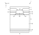
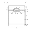
パワー半導体スイッチにおいて、
第1の負荷端子および第2の負荷端子に結合された半導体本体を含んでおり、かつ
第1の導電型のドーパントを有するドリフト領域と、第1の負荷端子に電気的に接続された、第1の導電型のドーパントを有するソース領域と、第2の導電型のドーパントを有し、かつソース領域をドリフト領域から離隔させる、本体領域として形成された第1のドープ領域と、を含んでおり、
−ドリフト領域、ソース領域および本体領域によって、端子間の負荷電流が順方向に沿って導通される導通状態、端子間に印加される順方向電圧が阻止される順方向阻止状態、および端子間に印加される逆方向電圧が阻止される逆方向阻止状態、において、パワー半導体スイッチを動作させることができ、
−パワー半導体スイッチは、少なくとも本体領域内に配置されたダメージ領域を含む、
パワー半導体スイッチ。
Power semiconductor device is implemented as a power semiconductor switch, an example of the first exemplary subgroup of embodiments, and examples Examples of the
In power semiconductor switches,
A drift region having a semiconductor body coupled to the first load terminal and the second load terminal and having a dopant of the first conductivity type; and a drift region electrically connected to the first load terminal. A source region having a dopant of a first conductivity type and a first doped region having a dopant of a second conductivity type and formed as a body region and separating the source region from the drift region; ,
A conducting state in which the load current between the terminals is conducted along the forward direction by the drift region, the source region and the body region, a forward blocking state in which the forward voltage applied between the terminals is blocked, and In the reverse blocking state in which the applied reverse voltage is blocked, the power semiconductor switch can be operated;
The power semiconductor switch includes at least a damaged region located in the body region;
Power semiconductor switch.
例2
再結合領域は、再結合領域内に存在する電荷担体の寿命および移動度のうちの少なくとも1つを低減するように構成されている、
例1のパワー半導体スイッチ。
Example 2
The recombination region is configured to reduce at least one of the lifetime and mobility of charge carriers present in the recombination region;
The power semiconductor switch of Example 1.
例3
再結合領域は、横方向に構造化されている、
例1または2のパワー半導体スイッチ。
Example 3
The recombination region is laterally structured,
The power semiconductor switch of Example 1 or 2.
例4
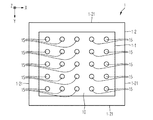
パワー半導体スイッチは、複数のトランジスタセルを備えた活性領域をさらに含んでおり、
再結合領域は、
−所定の割合の複数のトランジスタセルの各々のみが再結合領域を含むように、かつ/または
−再結合領域が、複数のトランジスタセルのうちの少なくとも1つの水平方向の横断面内で構造化されているように、
横方向に構造化されている、
例3のパワー半導体スイッチ。
Example 4
The power semiconductor switch further includes an active region having a plurality of transistor cells,
The recombination region is
-Only a predetermined proportion of the plurality of transistor cells each comprises a recombination region, and / or-the recombination region is structured in a horizontal cross-section of at least one of the plurality of transistor cells. As
Laterally structured,
The power semiconductor switch of Example 3.
例5
パワー半導体スイッチは、導通状態の間の負荷電流の少なくとも一部の導通のために、本体領域内に導通チャネルを誘導するようにさらに構成されており、
誘導された導通チャネルと再結合領域とは、相互に空間的に離隔されている、
例1から4までのいずれか1つのパワー半導体スイッチ。
Example 5
The power semiconductor switch is further configured to induce a conduction channel in the body region for conduction of at least a portion of the load current during the conduction state;
The induced conduction channel and the recombination region are spatially separated from each other,
Any one of the power semiconductor switches of Examples 1 to 4.
例6
再結合領域と誘導された導通チャネルとの間の最短距離は、少なくとも50nmである、
例5のパワー半導体スイッチ。
Example 6
The shortest distance between the recombination region and the induced conduction channel is at least 50 nm;
The power semiconductor switch of Example 5.
例7
再結合領域は、ソース領域内に広がっている、
例1から6までのいずれか1つのパワー半導体スイッチ。
Example 7
The recombination region extends into the source region,
The power semiconductor switch of any one of Examples 1 to 6.
例8
再結合領域は、ドリフト領域内には広がっていない、
例1から7までのいずれか1つのパワー半導体スイッチ。
Example 8
The recombination region does not extend into the drift region,
Any one of the power semiconductor switches of Examples 1 to 7.
例9
再結合領域は、ドリフト領域内の結晶欠陥濃度よりも少なくとも1,000倍高い結晶欠陥濃度を示す、
例8のパワー半導体スイッチ。
Example 9
The recombination region exhibits a crystal defect concentration at least 1,000 times higher than the crystal defect concentration in the drift region;
The power semiconductor switch of Example 8.
例10
本体領域は、半導体本体内で、再結合領域よりも深い位置まで広がっている、
例1から9までのいずれか1つのパワー半導体スイッチ。
Example 10
The body region extends deeper than the recombination region within the semiconductor body;
Any one of the power semiconductor switches of Examples 1 to 9.
例11
第1の負荷端子は、接触溝を含み、接触溝は、ソース領域および本体領域それぞれと相互作用し、
再結合領域は横方向において、接触溝と重なり合い、かつ接触溝の横方向の寸法の60%〜200%の範囲内の横方向の寸法を示す、
例1から10までのいずれか1つのパワー半導体スイッチ。
Example 11
The first load terminal includes a contact groove, wherein the contact groove interacts with each of the source region and the body region;
The recombination zone overlaps the contact groove in the lateral direction and exhibits a lateral dimension in the range of 60% to 200% of the lateral dimension of the contact groove;
The power semiconductor switch of any one of Examples 1 to 10.
例12
前述の導通状態、前述の順方向阻止状態および前述の逆方向阻止状態において動作するようにそれぞれ構成された複数のトランジスタセルを備えた活性領域と、活性領域を包囲する不活性エッジ領域と、を含んでおり、
再結合領域は、不活性エッジ領域内には広がっていない、
例1から11までのいずれか1つのパワー半導体スイッチ。
Example 12
An active region including a plurality of transistor cells each configured to operate in the aforementioned conductive state, the aforementioned forward blocking state, and the aforementioned backward blocking state, and an inactive edge region surrounding the active region. Includes,
The recombination region does not extend into the inactive edge region,
The power semiconductor switch of any one of Examples 1 to 11.
例13
再結合領域は、順方向阻止状態の間の電界のピークの場所から空間的に離れている、
例1から12までのいずれか1つのパワー半導体スイッチ。
Example 13
The recombination region is spatially separated from the location of the electric field peak during the forward blocking state,
Any one of the power semiconductor switches of Examples 1 to 12.
例14
再結合領域は、再結合領域内の複数の再結合中心を形成する結晶欠陥を示す、
例1から13までのいずれか1つのパワー半導体スイッチ。
Example 14
The recombination region indicates a crystal defect forming a plurality of recombination centers in the recombination region,
The power semiconductor switch of any one of Examples 1 to 13.
例15
結晶欠陥は、少なくとも360℃の温度までは温度安定性を有する、
例14のパワー半導体スイッチ。
Example 15
The crystal defects are temperature stable up to a temperature of at least 360 ° C.
The power semiconductor switch of Example 14.
例16
再結合領域は、少なくとも横方向に沿って、少なくとも2倍変化する結晶欠陥濃度を示す、
例1から15までのいずれか1つのパワー半導体スイッチ。
Example 16
The recombination region exhibits a crystal defect concentration that varies at least two-fold, at least along the lateral direction;
The power semiconductor switch of any one of Examples 1 to 15.
例17
再結合領域は、少なくとも垂直方向に沿って、少なくとも2倍変化する結晶欠陥濃度を示す、
例1から16までのいずれか1つのパワー半導体スイッチ。
Example 17
The recombination region exhibits a crystal defect concentration that varies at least two-fold along at least the vertical direction;
The power semiconductor switch of any one of Examples 1 to 16.
例18
本体領域は、第1のサブセクションおよび第2のサブセクションを示し、
第1のサブセクションは、第1の負荷端子と相互作用し、かつ第2のサブセクションよりも高いドーパント濃度を有しており、
第2のサブセクションは、ドリフト領域と相互作用し、
再結合領域は、第1のサブセクション内および第2のサブセクション内それぞれに広がっている、
例1から17までのいずれか1つのパワー半導体スイッチ。
Example 18
The body region indicates a first subsection and a second subsection,
The first subsection interacts with the first load terminal and has a higher dopant concentration than the second subsection;
The second subsection interacts with the drift region,
The recombination region extends within each of the first and second subsections;
The power semiconductor switch of any one of Examples 1 to 17.
例19
結晶欠陥濃度のピークは、第2のサブセクションの上側半分に配置されているか、または本体領域の第1のサブセクションの下側半分に配置されている、
例13および14のパワー半導体スイッチ。
Example 19
The crystal defect concentration peak is located in the upper half of the second subsection or is located in the lower half of the first subsection of the body region;
Power semiconductor switches of Examples 13 and 14.
例20
半導体本体は、第2の導電型のドーパントでドープされており、かつ第2の負荷端子に電気的に接続されているエミッタ領域を含み、
半導体本体は、専らエミッタ領域を介して、第2の負荷端子と相互作用する、
例1から19までのいずれか1つのパワー半導体スイッチ。
Example 20
The semiconductor body includes an emitter region doped with a dopant of a second conductivity type and electrically connected to a second load terminal;
The semiconductor body interacts with the second load terminal exclusively via the emitter region;
The power semiconductor switch of any one of Examples 1 to 19.
例21
半導体本体は、フィールドストップ領域をさらに含み、
フィールドストップ領域は、ドリフト領域を終端させ、かつドリフト領域のドーパント濃度よりも高い、第1の導電型のドーパントの、陽子照射誘導型のドーパント濃度を示す、
例1から20までのいずれか1つのパワー半導体スイッチ。
Example 21
The semiconductor body further includes a field stop region,
The field stop region terminates the drift region and exhibits a proton irradiation induced dopant concentration of the first conductivity type dopant that is higher than the drift region dopant concentration;
Any one of the power semiconductor switches of Examples 1 to 20.
例22
逆方向阻止IGBTにおいて、少なくとも、逆方向阻止IGBTの本体領域として形成された第1のドープ領域内に形成された、横方向に構造化された再結合領域を含む、
逆方向阻止IGBT。
Example 22
A reverse blocking IGBT, including at least a laterally structured recombination region formed in a first doped region formed as a body region of the reverse blocking IGBT;
Reverse blocking IGBT.
例23
パワー半導体スイッチを処理する方法において、
−第1の負荷端子および第2の負荷端子に結合されるべき半導体本体であって、第1の導電型のドーパントを有するドリフト領域と、第1の負荷端子に電気的に接続された、第1の導電型のドーパントを有するソース領域と、第2の導電型のドーパントを有し、かつソース領域をドリフト領域から離隔させる、本体領域として形成された第1のドープ領域と、を含む半導体本体を設けること、
−本体領域内に再結合領域を設けること、を含んでおり、
ドリフト領域、ソース領域および本体領域によって、端子間の負荷電流が順方向に沿って導通される導通状態、端子間に印加される順方向電圧が阻止される順方向阻止状態、および端子間に印加される逆方向電圧が阻止される逆方向阻止状態、において、パワー半導体スイッチを動作させることができる、
パワー半導体スイッチを処理する方法。
Example 23
In a method of processing a power semiconductor switch,
A semiconductor body to be coupled to the first load terminal and the second load terminal, wherein the drift region has a dopant of a first conductivity type and a second body electrically connected to the first load terminal; A semiconductor body comprising: a source region having a dopant of one conductivity type; and a first doped region having a dopant of a second conductivity type and spaced from the drift region and formed as a body region. Providing,
Providing a recombination region within the body region;
A conduction state in which the load current between the terminals is conducted along the forward direction by the drift region, the source region, and the body region, a forward blocking state in which the forward voltage applied between the terminals is blocked, and an application between the terminals. In the reverse blocking state in which the reverse voltage is blocked, the power semiconductor switch can be operated.
How to handle power semiconductor switches.
例24
再結合領域を設けることは、注入処理ステップおよび拡散処理ステップのうちの少なくとも1つによって、結晶欠陥を半導体本体内に導入することを含む、
例23の方法。
Example 24
Providing the recombination region includes introducing a crystal defect into the semiconductor body by at least one of the implantation processing step and the diffusion processing step.
The method of Example 23.
例25
再結合領域を設けることは、ソース領域および本体領域それぞれが第1の負荷端子によって接触されることになる溝を使用して、自己整合処理ステップを実行することを含む、
例23または24の方法。
Example 25
Providing a recombination region includes performing a self-alignment processing step using a groove where each of the source region and the body region will be contacted by the first load terminal.
The method of Example 23 or 24.
パワー半導体デバイスが、過電圧保護パワー半導体チップとして、または集積パワー半導体モジュールとして実施されている、実施の形態の第2の例示的なサブグループの例、および対応する方法の例
上記において示唆したように、実施の形態の第2の例示的なサブグループに関して、再結合領域を設けるか、または設けないかは任意であってよい。
Example of a second exemplary sub-group of embodiments, and examples of corresponding methods, in which the power semiconductor device is implemented as an overvoltage protected power semiconductor chip or as an integrated power semiconductor module, as suggested above With respect to the second exemplary sub-group of the embodiments, it may be optional to provide or not to provide a recombination region.
例1
過電圧保護パワー半導体チップにおいて、
過電圧保護パワー半導体チップは、チップの前面側に配置された第1の負荷端子およびチップの背面側に配置された第2の負荷端子に結合された半導体本体を含み、
半導体本体は、活性領域と、活性領域を包囲する不活性エッジ領域と、をそれぞれ含み、
活性領域は、複数のブレークスルーセルを含み、
各ブレークスルーセルは、
−第1の負荷端子が内部まで広がっており、かつ半導体本体と相互作用する凹部を有している、前面側に配置された絶縁構造と、
−第1の導電型のドーパントを有しているドリフト領域と、
−第2の導電型のドーパントを有しており、かつ第1の負荷端子に電気的に接続されている、アノード領域として形成された第1のドープ領域と、
−アノード領域よりも低いドーパント濃度の第2の導電型のドーパントを有しており、かつアノード領域および絶縁構造それぞれに接触して配置された第1のバリア領域と、
−ドリフト領域よりも高いドーパント濃度の第1の導電型のドーパントを有しており、かつアノード領域および第1のバリア領域の少なくとも一部それぞれをドリフト領域から離隔させる第2のバリア領域と、
−第2の負荷端子に接触して配置されたドープ接触領域と、を含み、
ドリフト領域は、第2のバリア領域とドープ接触領域との間に位置決めされている、
過電圧保護パワー半導体チップ。
Example 1
In overvoltage protection power semiconductor chip,
The overvoltage protection power semiconductor chip includes a semiconductor body coupled to a first load terminal disposed on a front side of the chip and a second load terminal disposed on a rear side of the chip;
The semiconductor body includes an active region and an inactive edge region surrounding the active region, respectively.
The active region includes a plurality of breakthrough cells,
Each breakthrough cell is
An insulation structure arranged on the front side, wherein the first load terminal extends into the interior and has a recess interacting with the semiconductor body;
A drift region having a dopant of the first conductivity type;
A first doped region having a dopant of the second conductivity type and electrically connected to the first load terminal, formed as an anode region;
A first barrier region having a dopant of a second conductivity type with a lower dopant concentration than the anode region, and disposed in contact with each of the anode region and the insulating structure;
A second barrier region having a dopant of a first conductivity type with a higher dopant concentration than the drift region and separating at least a portion of each of the anode region and the first barrier region from the drift region;
-A doped contact area arranged in contact with the second load terminal;
The drift region is positioned between the second barrier region and the doped contact region;
Overvoltage protection power semiconductor chip.
例2
各ブレークスルーセルは、
−負荷端子間の電圧が定格チップ阻止電圧を下回る場合に非導通状態に留まるように、
−負荷端子間の電圧が定格チップ阻止電圧を上回る場合に導通ブレークスルー状態を取るように、構成されている、
例1のチップ。
Example 2
Each breakthrough cell is
-To remain non-conductive when the voltage between the load terminals is below the rated chip blocking voltage,
-Configured to take a conductive breakthrough condition when the voltage between the load terminals exceeds the rated chip blocking voltage;
Example 1 chip.
例3
チップがパワー半導体トランジスタに結合されており、
各ブレークスルーセルが、トランジスタの定格阻止電圧に依存して定められた、定格チップ阻止電圧に関して構成されている、
例2のチップ。
Example 3
The chip is coupled to a power semiconductor transistor,
Each breakthrough cell is configured with respect to a rated chip blocking voltage, which is determined depending on the rated blocking voltage of the transistor;
Example 2 chip.
例4
各ブレークスルーセルは、少なくとも第1のドープ領域内に広がっている再結合領域を含む、
例1から3までのいずれか1つのチップ。
Example 4
Each breakthrough cell includes a recombination region extending at least within the first doped region;
Any one of the chips of Examples 1 to 3.
例5
再結合領域は、局所的に低下した電荷担体寿命を提供する、
例4のチップ。
Example 5
The recombination region provides a locally reduced charge carrier lifetime,
Example 4 chip.
例6
アノード領域は、半導体本体内の、第1のバリア領域よりも深い位置まで広がっており、
深さレベルの差異に起因して形成された段部が、第2の半導体バリア領域によって覆われている、
例1から5までのいずれか1つのチップ。
Example 6
The anode region extends to a position deeper than the first barrier region in the semiconductor body;
A step formed due to the difference in depth level is covered by the second semiconductor barrier region;
Any one of the chips of Examples 1 to 5.
例7
ブレークスルーセルの第1のバリア領域は、連続する半導体層を形成する、
例1から6までのいずれか1つのチップ。
Example 7
The first barrier region of the breakthrough cell forms a continuous semiconductor layer;
Any one of the chips of Examples 1 to 6.
例8
ブレークスルーセルは、六角形のテッセレーションパターンに従い、活性領域内に配置されている、
例1から7までのいずれか1つのチップ。
Example 8
Breakthrough cells are arranged in the active area according to a hexagonal tessellation pattern,
Any one of the chips of Examples 1 to 7.
例9
各ブレークスルーセル内に、アノード領域、第1のバリア領域および第2のバリア領域が、各ブレークスルーセルを横断する仮想の垂直方向軸線に関して対称的に配置されている、
例1から8までのいずれか1つのチップ。
Example 9
Within each breakthrough cell, an anode region, a first barrier region, and a second barrier region are symmetrically disposed with respect to a virtual vertical axis that traverses each breakthrough cell.
Any one of the chips of Examples 1 to 8.
例10
アノード領域、第1のバリア領域および第2のバリア領域それぞれに存在するドーパントは、注入されたドーパントである、
例1から9までのいずれか1つのチップ。
Example 10
The dopant present in each of the anode region, the first barrier region and the second barrier region is an implanted dopant;
Any one of the chips of Examples 1 to 9.
例11
第2の負荷端子とドープ接触領域との間の移行部は、ショットキーコンタクトを形成する、
例1から10までのいずれか1つのチップ。
Example 11
The transition between the second load terminal and the doped contact region forms a Schottky contact;
Any one of the chips of Examples 1 to 10.
例12
ドープ接触領域は、第2の導電型のドーパントを有するエミッタと、第1の導電型のドーパントを有するフィールドストップ領域と、を含み、
エミッタは、第2の負荷端子に電気的に接続されており、
フィールドストップ領域は、ドリフト領域とエミッタとの間に配置されている、
例1から11までのいずれか1つのチップ。
Example 12
The doped contact region includes an emitter having a second conductivity type dopant and a field stop region having a first conductivity type dopant;
The emitter is electrically connected to the second load terminal,
The field stop region is disposed between the drift region and the emitter,
Any one of the chips of Examples 1 to 11.
例13
チップは、半導体本体の前面側かつ外部に配置されたダイオード装置をさらに含み、
ダイオード装置は、横方向において不活性エッジ領域と重なり合い、かつ第1の負荷端子および別の端子に接続されている、
例1から12までのいずれか1つのチップ。
Example 13
The chip further includes a diode device disposed on the front side and outside of the semiconductor body,
A diode device laterally overlapping the inactive edge region and connected to the first load terminal and another terminal;
Any one of the chips of Examples 1 to 12.
例14
別の端子は、パワー半導体トランジスタのエミッタ端子に電気的に接続されている、
例13のチップ。
Example 14
Another terminal is electrically connected to the emitter terminal of the power semiconductor transistor,
Example 13 chip.
例15
不活性エッジ領域は、各ブレークスルーセルの降伏電圧よりも高い降伏電圧を示す、
例1から14までのいずれか1つのチップ。
Example 15
The inactive edge region exhibits a higher breakdown voltage than the breakdown voltage of each breakthrough cell,
Any one of the chips of Examples 1 to 14.
例16
チップは、1つまたは複数の第1のタイプの補助セルをさらに含み、
1つまたは複数の第1のタイプの補助セルはそれぞれ、
−第1の負荷端子が内部まで広がっており、かつ半導体本体と相互作用する凹部を有している、前面側に配置された絶縁構造と、
−第1の導電型のドーパントを有しているドリフト領域と、
−第1の負荷端子に電気的に接続されており、かつ第2の導電型のドーパントを有しているアノード領域と、
−アノード領域および絶縁構造それぞれに接触して配置された、アノード領域よりも低いドーパント濃度の第2の導電型のドーパントを有している第1のバリア領域と、
−アノード領域および第1のバリア領域の少なくとも一部それぞれをドリフト領域から離隔させる、ドリフト領域よりも高いドーパント濃度の第1の導電型のドーパントを有している第2のバリア領域と、
−第2の負荷端子に接触して配置されたドープ接触領域と、を含み、
ドリフト領域は、第2のバリア領域とドープ接触領域との間に位置決めされ、
ドープ接触領域は、半導体本体の層厚の50%までにわたり半導体本体内に広がっている、
例1から15までのいずれか1つのチップ。
Example 16
The chip further comprises one or more first type auxiliary cells;
The one or more first type auxiliary cells are each
An insulation structure arranged on the front side, wherein the first load terminal extends into the interior and has a recess interacting with the semiconductor body;
A drift region having a dopant of the first conductivity type;
An anode region electrically connected to the first load terminal and having a dopant of the second conductivity type;
-A first barrier region having a lower dopant concentration of the second conductivity type dopant than the anode region, disposed in contact with each of the anode region and the insulating structure;
-A second barrier region having a higher dopant concentration of the first conductivity type dopant than the drift region, separating the anode region and at least a portion of each of the first barrier region from the drift region;
-A doped contact area arranged in contact with the second load terminal;
A drift region positioned between the second barrier region and the doped contact region;
The doped contact region extends into the semiconductor body over up to 50% of the layer thickness of the semiconductor body;
Any one of the chips of Examples 1 to 15.
例17
チップは、1つまたは複数の第2のタイプの補助セルをさらに含み、
1つまたは複数の第2のタイプの補助セルはそれぞれ、
−第1の負荷端子が内部まで広がっており、かつ半導体本体と相互作用する、前面側に配置された絶縁構造と、
−第1の導電型のドーパントを有しているドリフト領域と、
−第1の負荷端子に電気的に接続されており、かつ第2の導電型のドーパントを有している第1のバリア領域と、
−第2の負荷端子に接触して配置されたドープ接触領域と、を含み、
ドリフト領域は、第1のバリア領域とドープ接触領域との間に位置決めされている、
例1から16までのいずれか1つのチップ。
Example 17
The chip further comprises one or more second type auxiliary cells;
The one or more second type auxiliary cells are each
An insulation structure arranged on the front side, wherein the first load terminal extends into the interior and interacts with the semiconductor body;
A drift region having a dopant of the first conductivity type;
A first barrier region electrically connected to the first load terminal and having a dopant of the second conductivity type;
-A doped contact area arranged in contact with the second load terminal;
A drift region positioned between the first barrier region and the doped contact region;
Any one of the chips of Examples 1 to 16.
例18
チップは、パワー半導体トランジスタに結合されており、
トランジスタは、複数のトランジスタセルを含んでおり、各トランジスタセルはチップに集積されている、
例1から17までのいずれか1つのチップ。
Example 18
The chip is coupled to a power semiconductor transistor,
The transistor includes a plurality of transistor cells, each transistor cell being integrated on a chip,
Any one of the chips of Examples 1 to 17.
例19
各トランジスタセルは、
−エミッタ端子に電気的に接続されており、かつ第1の導電型のドーパントを有しているソース領域と、
−第1の導電型のドーパントを有しているドリフト領域と、
−エミッタ端子に電気的に接続されており、かつソース領域をドリフト領域から絶縁させる、第2の導電型のドーパントを有している本体領域と、
−トランジスタセルを制御するように構成された絶縁ゲート電極と、
−第2の負荷端子に電気的に接続された、第2の導電型のドーパントを有しているドープ接触領域と、を含む、
例18のチップ。
Example 19
Each transistor cell is
A source region electrically connected to the emitter terminal and having a dopant of the first conductivity type;
A drift region having a dopant of the first conductivity type;
A body region electrically connected to the emitter terminal and having a dopant of the second conductivity type, isolating the source region from the drift region;
-An insulated gate electrode configured to control the transistor cell;
-A doped contact region having a dopant of a second conductivity type, electrically connected to the second load terminal;
Example 18 chip.
例20
ブレークスルーセルのドープ接触領域およびトランジスタセルのドープ接触領域は、半導体本体内にドープ接触層を形成する、
例18または19のチップ。
Example 20
The doped contact region of the breakthrough cell and the doped contact region of the transistor cell form a doped contact layer in the semiconductor body;
The chip of Example 18 or 19.
例21
パワー半導体トランジスタおよび過電圧保護パワー半導体チップを含む集積パワー半導体モジュールにおいて、
過電圧保護パワー半導体チップは、チップの前面側に配置された第1の負荷端子およびチップの背面側に配置された第2の負荷端子に結合された半導体本体を含み、
半導体本体は、活性領域と、活性領域を包囲する不活性エッジ領域と、をそれぞれ含み、
活性領域は、複数のブレークスルーセルを含み、
各ブレークスルーセルは、
−第1の負荷端子が内部まで広がっており、かつ半導体本体と相互作用する凹部を有している、前面側に配置された絶縁構造と、
−第1の導電型のドーパントを有しているドリフト領域と、
−第2の導電型のドーパントを有しており、かつ第1の負荷端子に電気的に接続されている、アノード領域として形成された第1のドープ領域と、
−アノード領域よりも低いドーパント濃度の第2の導電型のドーパントを有しており、かつアノード領域および絶縁構造それぞれに接触して配置された第1のバリア領域と、
−ドリフト領域よりも高いドーパント濃度の第1の導電型のドーパントを有しており、かつアノード領域および第1のバリア領域の少なくとも一部それぞれをドリフト領域から離隔させる第2のバリア領域と、
−第2の負荷端子に接触して配置されたドープ接触領域と、を含み、
ドリフト領域は、第2のバリア領域とドープ接触領域との間に位置決めされ、
トランジスタは、エミッタ端子、コレクタ端子およびゲート端子を含み、コレクタ端子は、チップの第2の負荷端子に電気的に接続されている、
集積パワー半導体モジュール。
Example 21
In an integrated power semiconductor module including a power semiconductor transistor and an overvoltage protection power semiconductor chip,
The overvoltage protection power semiconductor chip includes a semiconductor body coupled to a first load terminal disposed on a front side of the chip and a second load terminal disposed on a rear side of the chip;
The semiconductor body includes an active region and an inactive edge region surrounding the active region, respectively.
The active region includes a plurality of breakthrough cells,
Each breakthrough cell is
An insulation structure arranged on the front side, wherein the first load terminal extends into the interior and has a recess interacting with the semiconductor body;
A drift region having a dopant of the first conductivity type;
A first doped region having a dopant of the second conductivity type and electrically connected to the first load terminal, formed as an anode region;
A first barrier region having a dopant of a second conductivity type with a lower dopant concentration than the anode region, and disposed in contact with each of the anode region and the insulating structure;
A second barrier region having a dopant of a first conductivity type with a higher dopant concentration than the drift region and separating at least a portion of each of the anode region and the first barrier region from the drift region;
-A doped contact area arranged in contact with the second load terminal;
A drift region positioned between the second barrier region and the doped contact region;
The transistor includes an emitter terminal, a collector terminal, and a gate terminal, wherein the collector terminal is electrically connected to a second load terminal of the chip.
Integrated power semiconductor module.
例22
過電圧保護パワー半導体チップを処理する方法において、
−チップの前面側に配置されるべき第1の負荷端子およびチップの背面側に配置されるべき第2の負荷端子に結合されるべき半導体本体であって、活性領域と、活性領域を包囲する不活性エッジ領域と、をそれぞれ含む半導体本体を設けること、
−第1の負荷端子が内部まで広がっており、かつ半導体本体と相互作用する凹部を有している、前面側に配置された絶縁構造をそれぞれが含んでいる複数のブレークスルーセルを活性領域内に、形成すること、
−以下の領域、すなわち
−第1の導電型のドーパントを有しているドリフト領域と、
−第2の導電型のドーパントを有しており、かつ第1の負荷端子に電気的に接続されている、アノード領域として形成された第1のドープ領域と、
−アノード領域よりも低いドーパント濃度の第2の導電型のドーパントを有しており、かつアノード領域および絶縁構造それぞれに接触して配置された第1のバリア領域と、
−ドリフト領域よりも高いドーパント濃度の第1の導電型のドーパントを有しており、かつアノード領域および第1のバリア領域の少なくとも一部それぞれをドリフト領域から離隔させる第2のバリア領域と、
−第2の負荷端子に接触して配置されたドープ接触領域と、を形成すること、を含み、
ドリフト領域は、第2のバリア領域とドープ接触領域との間に位置決めされている、
方法。
Example 22
In a method of processing an overvoltage protection power semiconductor chip,
A semiconductor body to be coupled to a first load terminal to be arranged on the front side of the chip and to a second load terminal to be arranged on the back side of the chip, surrounding the active area and the active area; Providing an inactive edge region, and a semiconductor body each including:
A plurality of breakthrough cells in the active region, each including a front-side insulating structure, wherein the first load terminals extend into the interior and have recesses for interacting with the semiconductor body; , Forming,
-A drift region having a dopant of the first conductivity type;
A first doped region having a dopant of the second conductivity type and electrically connected to the first load terminal, formed as an anode region;
A first barrier region having a dopant of a second conductivity type with a lower dopant concentration than the anode region, and disposed in contact with each of the anode region and the insulating structure;
A second barrier region having a dopant of a first conductivity type with a higher dopant concentration than the drift region and separating at least a portion of each of the anode region and the first barrier region from the drift region;
-Forming a doped contact region disposed in contact with the second load terminal;
The drift region is positioned between the second barrier region and the doped contact region;
Method.
例23
アノード領域を形成すること、第1のバリア領域を形成すること、および第2のバリア領域を形成することのうちの少なくとも1つは、注入処理ステップを少なくとも1回実行することを含む、
例22の方法。
Example 23
At least one of forming an anode region, forming a first barrier region, and forming a second barrier region includes performing an implantation process step at least once.
The method of Example 22.
例24
1回または複数回の注入処理ステップのうちの少なくとも1回を、少なくとも1.5MeVのイオンエネルギでもって実行する、
例23の方法。
Example 24
Performing at least one of the one or more implant processing steps with an ion energy of at least 1.5 MeV;
The method of Example 23.
例25
絶縁構造をマスクとして使用する自動調整プロセスを実行することによって、少なくともアノード領域内まで広がる再結合領域を形成することをさらに含む、
例22から24までのいずれか1つの方法。
Example 25
Further comprising forming a recombination region that extends at least into the anode region by performing an automatic conditioning process using the insulating structure as a mask.
The method of any one of Examples 22 to 24.
当業者であれば、以下の詳細な説明を読み、また添付の図面を見ることによって、付加的な特徴および利点を理解するであろう。 Those skilled in the art will appreciate additional features and advantages by reading the following detailed description, and by viewing the accompanying drawings.
図面における各部分は、必ずしも縮尺通りではなく、その代わりに、本発明の原理を説明することに重点を置いて強調されている。さらに、図面において、同様の参照番号は対応する部分を表している。 Each section in the drawings is not necessarily to scale, emphasis instead being placed upon illustrating the principles of the invention. Moreover, in the drawings, like reference numbers indicate corresponding parts.
以下の詳細な説明においては、本願の一部を成し、かつ本発明を実施することができる特定の実施の形態が図示を目的として示されている添付の図面を参照する。 In the following detailed description, reference is made to the accompanying drawings that form a part hereof, and in which is shown by way of illustration specific embodiments in which the invention may be practiced.
これに関して、方向を表す用語、例えば「上部」、「下部」、「下」、「前」、「奥」、「後ろ」、「前方」、「後方」、「上方」などは、説明される図面の向きに関して使用されていると考えられる。実施の形態の各部分を、種々異なる向きで位置決めすることができるので、方向を表す用語は、図示を目的として使用されているのであって、いずれの限定も意図していない。本発明の範囲から逸脱することなく、他の実施の形態を使用することができ、また構造的または論理的な変更を成すことができると解されるべきである。したがって、以下の詳細な説明は、限定的な意味で理解されるべきではなく、本発明の範囲は、添付の特許請求の範囲によって定義される。 In this regard, directional terms such as “top”, “bottom”, “bottom”, “front”, “back”, “back”, “front”, “back”, “up”, etc. are described. It is believed that it is used with respect to the orientation of the drawing. Because the parts of the embodiments can be positioned in different orientations, the directional terminology is used for illustrative purposes and is not intended to be limiting. It is to be understood that other embodiments can be used and structural or logical changes can be made without departing from the scope of the invention. Therefore, the following detailed description is not to be taken in a limiting sense, and the scope of the present invention is defined by the appended claims.
次に、図面に図示した種々の実施の形態、1つまたは複数の実施例を詳細に参照する。各実施例は、説明を目的として提供されており、本発明の限定を意図するものではない。例えば、1つの実施の形態の一部として図示または説明されている特徴を、他の実施の形態において、または他の実施の形態と組み合わせて使用して、別の実施の形態を創作することができる。本発明は、そのような修正および変更を含むことが意図されている。実施例を、添付の特許請求の範囲を限定するものと解されるべきではない特定の言語を用いて説明する。図面は縮尺通りではなく、単に図示を目的としている。分かり易くするために、別個の記載がない限り、同一の構成要素または製造ステップは異なる図面においても同一の参照番号によって表されている。 Reference will now be made in detail to various embodiments, one or more examples, of which are illustrated in the drawings. Each example is provided by way of explanation, and is not intended to limit the invention. For example, features illustrated or described as part of one embodiment may be used on or in combination with another embodiment to yield a different embodiment. it can. The present invention is intended to include such modifications and changes. The embodiments will be described using a particular language which should not be construed as limiting the appended claims. The drawings are not to scale and are for illustrative purposes only. For the sake of clarity, identical components or manufacturing steps are denoted by the same reference numerals in different drawings, unless otherwise noted.
本明細書において使用されているような「水平」という用語は、半導体基板または半導体構造の水平な表面に実質的に平行な向きを表すことが意図されている。この水平な表面は、例えば、半導体ウェハまたはダイまたはチップの表面であってよい。例えば、下記において言及する第1の横方向Xおよび第2の横方向Yはいずれも水平な方向であると考えられ、この場合、第1の横方向Xおよび第2の横方向Yは、相互に直交していると考えられる。 The term "horizontal" as used herein is intended to denote an orientation substantially parallel to the horizontal surface of the semiconductor substrate or structure. This horizontal surface may be, for example, the surface of a semiconductor wafer or die or chip. For example, the first lateral direction X and the second lateral direction Y referred to below are both considered to be horizontal directions, in which case the first lateral direction X and the second lateral direction Y are mutually Is considered to be orthogonal to
本明細書において使用されている「垂直」という用語は、水平な表面に対して実質的に直角に、すなわち半導体ウェハ/チップ/ダイの表面の法線方向に実質的に平行に整列されている向きを表すことが意図されている。例えば、下記において言及する伸張方向Zは、第1の横方向Xおよび第2の横方向Yのいずれに対しても垂直な伸張方向であると考えられる。伸張方向Zは、本明細書において、「垂直方向Z」とも称する。 As used herein, the term "vertical" is aligned substantially perpendicular to a horizontal surface, that is, substantially parallel to the normal to the surface of the semiconductor wafer / chip / die. It is intended to represent orientation. For example, the extension direction Z referred to below is considered to be an extension direction perpendicular to both the first lateral direction X and the second lateral direction Y. The extension direction Z is also referred to as “vertical direction Z” in this specification.
本明細書において、n型ドープとは「第1の導電型」を表し、それに対し、p型ドープとは「第2の導電型」を表す。択一的に、逆のドーピングの関係を使用することもできる。つまり、第1の導電型をp型ドープにして、第2の導電型をn型ドープにすることができる。 In the present specification, the n-type doping represents “first conductivity type”, while the p-type doping represents “second conductivity type”. Alternatively, the opposite doping relationship can be used. That is, the first conductivity type can be p-type doped and the second conductivity type can be n-type doped.
本明細書のコンテキストにおいて、用語「オーミック接触されている」、「電気的に接触されている」、「オーミック接続されている」および「電気的に接続されている」とは、半導体デバイスの2つの領域、セクション、ゾーン、区画または部分間、もしくは1つまたは複数のデバイスの異なる端子間、もしくは端子または金属化部または電極と、半導体デバイスの一区画または一部との間に、低抵抗の電気的な接続部または低抵抗の電流経路が存在することを表すことが意図されている。さらに、本明細書のコンテキストにおいて、用語「接触している」は、各半導体デバイスの2つの構成要素間の直接的で物理的な接続が存在することを表すことが意図されている。つまり例えば、相互に接触している2つの構成要素間の移行部が、介在する別の構成要素などを含むことはない。 In the context of this specification, the terms “ohmically contacted”, “electrically contacted”, “ohmically connected” and “electrically connected” refer to two of a semiconductor device. One region, section, zone, section or section, or between different terminals of one or more devices, or between a terminal or metallization or electrode and a section or part of a semiconductor device. It is intended to indicate that an electrical connection or low resistance current path exists. Further, in the context of the present specification, the term "contacting" is intended to indicate that there is a direct physical connection between the two components of each semiconductor device. That is, for example, a transition between two components that are in contact with each other does not include another intervening component or the like.
さらに、本明細書のコンテキストにおいて、用語「電気的な絶縁」は、別個の記載がない限り、その一般的に有効な理解のコンテキストにおいて使用されており、したがって2つまたはそれ以上の構成要素が相互に離隔されて配置されており、かつそれらの構成要素を接続するオーミック接続は存在しないことを表すことが意図されている。しかしながらそれにもかかわらず、相互に電気的に絶縁されている構成要素を、相互に結合させることができ、例えば機械的に結合させることができる、かつ/または容量性に結合させることができる、かつ/または誘導性に結合させることができる。一例を挙げると、キャパシタの2つの電極を、相互に電気的に絶縁させることができ、またそれと同時に、機械的かつ容量性に、例えば絶縁体、例えば誘電体によって相互に結合させることができる。 Further, in the context of this specification, the term "electrical isolation" is used in its generally valid understanding context unless otherwise stated, so that two or more components It is intended to indicate that there are no ohmic connections that are spaced apart from each other and connect those components. However, nevertheless, components that are electrically isolated from each other can be coupled to one another, for example mechanically coupled and / or capacitively coupled, and And / or can be inductively linked. By way of example, the two electrodes of a capacitor can be electrically insulated from one another and at the same time mechanically and capacitively coupled to one another, for example by an insulator, for example a dielectric.
本明細書において説明する特定の実施の形態は、帯状のセルまたはセルラ状のセルの構成を示すパワー半導体スイッチ、例えば電力変換器または電源において使用することができるパワー半導体デバイスに属するが、これに限定されるわけではない。したがって、1つの実施の形態においては、負荷に供給されるべき負荷電流、および/または電源から供給される負荷電流を流すように、そのようなデバイスを構成することができる。例えば、パワー半導体デバイスは、1つまたは複数のアクティブな電力半導体セル、例えばモノリシックに集積されたダイオードセル、例えばモノリシックに集積された、逆直列に接続された2つのダイオードから成るセル、モノリシックに集積されたトランジスタセル、例えばモノリシックに集積されたIGBTセルおよび/またはそれらの派生物を含むことができる。そのようなダイオード/トランジスタセルを、パワー半導体モジュールに集積することができる。そのような複数のセルは、パワー半導体デバイスの活性領域も一緒に配置されるセルフィールドを構成することができる。 Certain embodiments described herein pertain to power semiconductor switches that can be used in power semiconductor switches, for example, power converters or power supplies, that exhibit a configuration of strip cells or cellular cells. It is not limited. Thus, in one embodiment, such a device can be configured to carry a load current to be supplied to a load and / or a load current supplied from a power supply. For example, a power semiconductor device may comprise one or more active power semiconductor cells, e.g., a monolithically integrated diode cell, e.g., a monolithically integrated cell comprising two diodes connected in anti-series, a monolithically integrated Transistor cells, such as monolithically integrated IGBT cells and / or derivatives thereof. Such a diode / transistor cell can be integrated in a power semiconductor module. Such a plurality of cells can constitute a cell field in which the active region of the power semiconductor device is also arranged.
本明細書において使用されているような「パワー半導体デバイス」という用語は、高電圧阻止能力および/または大電流通電能力を備えた単一のチップにおける半導体デバイスを表すことが意図されている。換言すれば、そのようなパワー半導体デバイスは、典型的には、例えば数10〜数100アンペアまでのアンペア範囲の大電流のために、かつ/または典型的には15Vを上回る、より典型的には100V以上、例えば少なくとも400Vまで、さらには例えば少なくとも3kVまでの高電圧のために使用されることが意図されている。 The term "power semiconductor device" as used herein is intended to describe a semiconductor device on a single chip with high voltage blocking capability and / or high current carrying capability. In other words, such power semiconductor devices are typically for large currents, for example in the range of tens to hundreds of amps, and / or typically more than 15V, more typically Is intended to be used for high voltages above 100 V, for example up to at least 400 V and even for example up to at least 3 kV.
例えば、下記に説明するパワー半導体デバイスは、帯状のセル構成またはセルラ状(柱状)のセル構成を示す半導体デバイスであってよく、また低電圧、中電圧および/または高電圧の用途におけるパワーコンポーネントとして使用されるように構成することができる。 For example, the power semiconductor device described below may be a semiconductor device exhibiting a strip-like cell configuration or a cellular (pillar-like) cell configuration, and as a power component in low, medium and / or high voltage applications. It can be configured to be used.
例えば、本明細書において使用されているような「パワー半導体デバイス」という用語は、例えばデータの記憶、データの計算、かつ/または他のタイプの半導体ベースのデータ処理に使用されるロジック半導体デバイスを指すものではない。 For example, the term "power semiconductor device" as used herein refers to a logic semiconductor device used, for example, for data storage, data computation, and / or other types of semiconductor-based data processing. It does not point.
図23は、幾つかの実施の形態によるパワー半導体デバイス1を、電気的な等価回路図と共に、概略的かつ例示的に示す。パワー半導体デバイス1を、例えば、(図17A〜図22に関連させて例示的に説明するような)パワー半導体スイッチとして、または(図1〜図16に関連させて例示的に説明するような)過電圧保護パワー半導体チップとして実施することができる。
FIG. 23 schematically and exemplarily shows the
したがって、以下において図23に関連させて説明するすべての事項は、別の図面に関連させて説明するすべての実施の形態に等しく適用されると解されるべきである。 Therefore, it should be understood that all matters described below with reference to FIG. 23 apply equally to all embodiments described with reference to another drawing.
パワー半導体デバイス1は、第1の負荷端子11(例えば、エミッタ端子、アノード端子またはソース端子)および第2の負荷端子12(例えば、コレクタ端子またはドレイン端子)に結合された半導体本体10を含む。半導体本体10は、
−第1の負荷端子11に電気的に接続された、第2の導電型の第1のドープ領域102(本明細書においては、本体領域102またはアノード領域102とも称する)と、
−第2の負荷端子12に電気的に接続された、第2の導電型のエミッタ領域1091と、
−第1のドープ領域102とエミッタ領域1091との間に配置された、第1の導電型のドリフト領域100と、を含み、
ここで、ドリフト領域100および第1のドープ領域102によって、
−負荷端子11、12間の負荷電流が順方向に沿って導通される導通状態、
−端子11、12間に印加された順方向電圧が阻止される順方向阻止状態、および
−端子11、12間に印加された逆方向電圧が阻止される逆方向阻止状態、においてパワー半導体デバイスを動作させることができる。
The
A first
A second conductivity
A first conductivity
Here, the
A conduction state in which the load current between the
The power semiconductor device is operated in a forward blocking state in which a forward voltage applied between
半導体本体10は、オプションとして、少なくとも第1のドープ領域102内に配置された再結合領域159をさらに含むことができる。
The
例えば、等価回路図に図示したように、第1のドープ領域102からドリフト領域100への移行部は、第1のダイオード51を形成しており、またエミッタ領域1091からドリフト領域100への移行部は、第2のダイオード52を形成している。第1のダイオード51および第2のダイオード52は、相互に逆直列に接続されている。
For example, as shown in the equivalent circuit diagram, the transition from the first
例えば、第1のダイオード51は第1のブレークスルー電圧を示し、また第2のダイオード52は第2のブレークスルー電圧を示し、ここで第1のブレークスルー電圧は、第2のブレークスルー電圧よりも少なくとも5倍高い。この倍率は、それどころか5より大きくてよく、例えば、少なくとも10、または100、またはそれどころか1,000を上回ってもよい。例えば、第2のブレークスルー電圧は、10Vより高くてよい、または50Vより高くてよい、例えば10Vより高く、かつ100V未満であってよい。例えば、第1のブレークスルー電圧は、第2のブレークスルー電圧よりも約80倍高く、したがって、例えば上述の値に基づき、800Vから8kVの範囲内にある。典型的な例は、第2のブレークスルー電圧に関しては20Vであり、また第1のブレークスルー電圧に関しては1,600Vである。
For example, a
例えば、第1の負荷端子11、第1のドープ領域102、再結合領域159、ドリフト領域100、エミッタ領域1091および第2の負荷端子12はそれぞれ、例えば第1の横方向Xに沿って、例えば少なくとも500nmの、または少なくとも2,000nmの、またはそれどころか6,000nmを上回る、共通の横方向の広がり範囲を示す。
For example, each of the
さらに、再結合領域159内に存在する電荷担体の寿命および移動度のうちの少なくとも1つを低減するように、再結合領域159を構成することができる。
Further,
下記においてより詳細に説明するように、再結合領域159を横方向に構造化することができる。
As described in more detail below, the
また下記においてより詳細に説明するように、導通状態の間の負荷電流の少なくとも一部の導通のために、第1のドープ領域102内に導通チャネル103を誘導するように、パワー半導体デバイス1を構成することができ、この場合、誘導された導通チャネル103と再結合領域159とは、相互に空間的に離隔されている。例えば、再結合領域と誘導された導通チャネルとの間の最短距離は、少なくとも50nmである。
Also, as described in more detail below, the
さらに、再結合領域159がドリフト領域100内に広がらないように、再結合領域159を配置することができる。
Further, the
1つの実施の形態においては、再結合領域159が、ドリフト領域100内の結晶欠陥濃度よりも少なくとも1,000倍高い結晶欠陥濃度を示す。
In one embodiment,
1つの実施の形態においては、第1のドープ領域102が、半導体本体10内で、再結合領域159よりも深い位置まで広がっている。
In one embodiment, first
下記のさらなる説明からより明らかになるように、第1の負荷端子11は、接触溝(図2における参照番号161および図19Aにおける参照番号111を参照されたい)を含むことができ、この接触溝は、第1のドープ領域102と相互作用し、この場合、再結合領域159は横方向において、接触溝と重なり合っており、かつ接触溝の横方向の寸法の60%〜200%の範囲内の横方向の寸法を示す。
As will become more apparent from the further description below, the
さらに、パワー半導体デバイス1は、複数のセル(例えば、トランジスタセル(図12および図13の参照番号14を参照されたい))を含むことができ、各セルは、前述の導通状態、前述の順方向阻止状態および前述の逆方向阻止状態において動作するように構成されている。
Further, the
再結合領域159は、順方向阻止状態の間の電界のピークの場所から空間的に離れているように、再結合領域159を設計することができる。
The
1つの実施の形態においては、再結合領域159が、その再結合領域159内で複数の再結合中心を形成する結晶欠陥を示すことができる。例えば、結晶欠陥は、少なくとも360℃の温度までは温度安定性を有している。再結合領域の結晶欠陥濃度を、少なくとも第1の横方向Xに沿って、少なくとも2倍変化させることができる。
In one embodiment, the
図19Aの説明からより明らかになるように、第1のドープ領域102は、第1のサブセクション(図19Aの参照番号1023を参照されたい)および第2のサブセクション(図19Aの参照番号1022を参照されたい)を示すことができ、第1のサブセクションは、第1の負荷端子11と相互作用し、かつ第2のサブセクションよりも高いドーパント濃度を有しており、また第2のサブセクションは、ドリフト領域100と相互作用し、再結合領域159は、第1のサブセクション内および第2のサブセクション内それぞれに広がっている。さらに、結晶欠陥濃度のピークを、第2のサブセクションの上側半分に配置することができるか、または第1のドープ領域102の第1のサブセクションの下側半分に配置することができる。
As will become more apparent from the description of FIG. 19A, the first
1つの実施の形態においては、半導体本体10が、専らエミッタ領域1091を介して、第2の負荷端子12と相互作用する。
In one embodiment, the
下記の説明からより明らかになるように、半導体本体10は、フィールドストップ領域1092をさらに含むことができ(図17B、図18B参照)、このフィールドストップ領域1092は、ドリフト領域100を終端させ、かつドリフト領域のドーパント濃度よりも高い、第1の導電型のドーパントの、陽子照射誘導型のドーパント濃度を示す。
As will become more apparent from the description below, the
パワー半導体デバイス1は、パワー半導体スイッチであってよく、また上記において示唆したように、第1の負荷端子11に電気的に接続された、第1の導電型のソース領域(図17Aにおける参照番号101を参照されたい)を含むことができ、この場合、第1のドープ領域102によって、ソース領域101がドリフト領域100から離隔される。例えば、再結合領域159が、ソース領域101内に広がっている。
The
1つの実施の形態においては、パワー半導体デバイス1が、活性領域(図1における参照番号1−1)と、その活性領域1−1を包囲する不活性エッジ領域1−2と、を含む。例えば、再結合領域159は、不活性エッジ領域1−2内には広がらない。
In one embodiment, the
さらに、1つの例においては、活性領域1−1が、複数のセル(例えば、トランジスタセル14)を含むことができ、この場合、再結合領域159は、以下のように横方向に構造化されている。つまり、所定の割合の複数のセル(例えば、トランジスタセル14)の各々のみが再結合領域159を含むように、かつ/または再結合領域159が複数のセル(例えば、トランジスタセル)のうちの少なくとも1つの水平方向の横断面内で構造化されているように、構造化されている。
Further, in one example, active region 1-1 can include multiple cells (eg, transistor cell 14), where
下記の説明からより明らかになるように、パワー半導体デバイス1は、第1のドープ領域102および絶縁構造16、142の両方に接触して配置された、第1のドープ領域102よりも低いドーパント濃度の第2の導電型の第1のバリア領域152(図2Aを参照されたい)と、第1のドープ領域102および第1のバリア領域152の少なくとも一部の両方をドリフト領域100から離隔させる、ドリフト領域100よりも高いドーパント濃度の第1の導電型の第2のバリア領域153と、をさらに含むことができる。例えば、第1のバリア領域152および第2のバリア領域153のうちの少なくとも1つは、活性領域1−1内の連続する半導体層を形成する(図24を参照されたい)。
As will become more apparent from the description below, the
本明細書においては、パワー半導体デバイスを処理する方法も開示される。半導体デバイスは、第1の負荷端子および第2の負荷端子に結合された半導体本体を含む。半導体本体は、第1の負荷端子に電気的に接続された、第2の導電型の第1のドープ領域と、第2の負荷端子に電気的に接続された、第2の導電型のエミッタ領域と、第1のドープ領域とエミッタ領域との間に配置された、第1の導電型のドリフト領域と、を含む。ドリフト領域および第1のドープ領域によって、負荷端子間の負荷電流が順方向に沿って導通される導通状態、端子間に印加される順方向電圧が阻止される順方向阻止状態、および端子間に印加される逆方向電圧が阻止される逆方向阻止状態、において、パワー半導体デバイスを動作させることができる。方法は、半導体本体において、少なくとも第1のドープ領域内に配置された再結合領域を形成することを含む。 A method for processing a power semiconductor device is also disclosed herein. The semiconductor device includes a semiconductor body coupled to a first load terminal and a second load terminal. The semiconductor body includes a first doped region of a second conductivity type electrically connected to the first load terminal, and an emitter of a second conductivity type electrically connected to the second load terminal. A region, and a first conductivity type drift region disposed between the first doped region and the emitter region. A conduction state in which the load current between the load terminals is conducted along the forward direction by the drift region and the first doped region, a forward blocking state in which a forward voltage applied between the terminals is blocked, and In the reverse blocking state in which the applied reverse voltage is blocked, the power semiconductor device can be operated. The method includes forming, in the semiconductor body, a recombination region located at least within the first doped region.
方法の実施例は、上記において説明したデバイスの実施例に対応すると考えられる。方法のさらなるオプションとしての態様を、下記においてより詳細に説明する。 Embodiments of the method are believed to correspond to the device embodiments described above. Further optional aspects of the method are described in more detail below.
冒頭で説明したように、本明細書において説明するパワー半導体デバイス1、例えば上記において図23に関連させて説明したパワー半導体デバイス1を、例えば、パワー半導体スイッチとして、または過電圧保護パワー半導体チップとして実施することができる。
As described at the outset, the
図1〜図16の下記の説明ならびに図24、図25Aおよび図25Bの下記の説明は、主に、パワー半導体デバイス1が過電圧保護パワー半導体チップ(冒頭で言及した「実施の形態の第1の例示的なサブグループ」)として実施されている場合に関し、また図17A〜図22の下記の説明は、パワー半導体デバイス1がパワー半導体スイッチ(冒頭で言及した「実施の形態の第2の例示的なサブグループ」)として実施されている場合に関する。
The following description of FIG. 1 to FIG. 16 and the following description of FIG. 24, FIG. 25A and FIG. 25B mainly show that the
図1〜図22、図24、図25Aおよび図25Bの説明においては、パワー半導体デバイス1の構成要素のオプションとしての特徴を、特に第1のドープ領域102のオプションとしての特徴を説明する。それらのオプションとしての特徴は、(a)各デバイスがパワー半導体スイッチとして実施されているか、または過電圧保護パワー半導体チップとして実施されているかに関係なく、図1〜図22、図24、図25Aおよび図25Bに等しく適用することができ、(b)上記において説明した図23によるデバイスに等しく適用することができる、と解されるべきである。
In the description of FIGS. 1 to 22, 24, 25A and 25B, the optional features of the components of the
パワー半導体スイッチ
以下の説明は、パワー半導体デバイス1がパワー半導体スイッチとして実施されている、上記において言及した実施の形態の第1の例示的なサブグループの例、および対応する方法の例に関する。
Power semiconductor switch The following description relates to a first exemplary subgroup example of the above-mentioned embodiment, in which the
図21は、1つまたは複数の実施の形態によるパワー半導体スイッチ1の平面図を概略的かつ例示的に示す。図17A〜図18Bそれぞれは、1つまたは複数の実施の形態によるパワー半導体スイッチ1の実施の形態の縦断面図を概略的かつ例示的に示す。以下では、図21および図17A〜図18Bそれぞれを参照する。
FIG. 21 schematically and exemplarily shows a plan view of a
例えば、パワー半導体スイッチ1は、第1の負荷端子11(例えば、エミッタ端子11)および第2の端子(例えば、コレクタ端子12)に結合された半導体本体10を含む。
For example, the
本明細書に開示する図17A〜図22のすべての実施の形態に関して、パワー半導体スイッチ1は、逆方向阻止(RB:reverse blocking)IGBTであってよい。例えば、図17A〜図22それぞれは、RB IGBTを実現するように実施することができるパワー半導体スイッチの態様を示す。
17A to 22 disclosed in this specification, the
半導体本体10は、第1の導電型のドーパントを有するドリフト領域100を含むことができる。例えば、伸張方向Zに沿ったドリフト領域100の広がりおよびドリフト領域100のドーパント濃度が、設計されるべきパワー半導体スイッチ1のための定格阻止電圧に依存して、例えば当業者には公知であるようなやり方で選択される。
The
さらに、エミッタ端子11を、パワー半導体スイッチ1の前面側に配置することができ、また前面側金属化部を含むことができる。コレクタ端子12を、パワー半導体スイッチ1の前面側とは反対側、例えば背面側に配置することができ、また例えば、背面側金属化部を含むことができる。したがって、パワー半導体スイッチ1は、垂直方向の構成を示すことができ、この場合、負荷電流は、垂直方向に実質的に平行な方向に流れる。別の実施の形態においては、エミッタ端子11およびコレクタ端子12の両方を、パワー半導体スイッチ1の共通の側に配置することができ、例えば両方の端子をパワー半導体スイッチ1の前面に配置することができる。
Furthermore, the
パワー半導体スイッチ1は、活性領域1−1、不活性エッジ領域1−2(本明細書においては「終端構造」または「不活性終端構造」とも称する)、およびチップエッジ1−21(図21を参照されたい)をさらに含むことができる。半導体本体10は、活性領域1−1および不活性エッジ領域1−2それぞれの一部を形成することができ、この場合、チップエッジ1−21は、横方向において半導体本体10を終端させることができる。チップエッジ1−21を、例えばウェハダイシングによって形成することができ、また垂直方向Zに沿って広げることができる。図21に図示したように、不活性エッジ領域1−21を、活性領域1−1とチップエッジ1−2との間に配置することができる。
The
本明細書において、用語「活性領域」および「不活性エッジ領域/(不活性)終端構造」は、共通して用いられる。つまり、活性領域1−1および不活性エッジ領域1−2を、一般的にそれらに関連付けられた技術的な機能原理を提供するように構成することができる。例えば、パワー半導体スイッチ1の活性領域1−1を、端子11、12間で負荷電流が導通されるように構成することができ、それに対して、不活性エッジ領域1−2を、負荷電流は導通させないが、しかしながら電界の方向に関する機能を満たすように構成することができ、これによって、実施の形態に応じて、阻止能力の保証、活性領域1−1の安全な終端、などを実現することができる。例えば、図21に図示したように、不活性エッジ領域1−2は、活性領域1−1全体を包囲することができる。
In this specification, the terms "active region" and "inactive edge region / (inactive) termination structure" are commonly used. That is, the active region 1-1 and the inactive edge region 1-2 can be configured to provide the technical functional principles generally associated therewith. For example, the active region 1-1 of the
1つの実施の形態においては、活性領域1−1および不活性エッジ領域1−2それぞれが、下記においてより詳細に説明するように、パワー半導体スイッチの逆方向阻止能力を提供するように構成されている。 In one embodiment, each of active region 1-1 and inactive edge region 1-2 is configured to provide the reverse blocking capability of a power semiconductor switch, as described in more detail below. I have.
活性領域1−1は、少なくとも1つのトランジスタセル14(図21を参照されたい)を含むことができる。1つの実施の形態においては、そのようなトランジスタセル14が活性領域1−1内に複数含まれている。トランジスタセル14の数は、100より多くてよく、または1,000より多くてよい、またはそれどころか10,000より多くてよい。トランジスタセル14は、それぞれ同一の構成を示すことができる。したがって、1つの実施の形態においては、各トランジスタセル14が、例えば図17A〜図19Aに図示したように、パワーユニットセルの構成を示すことができる。以下では、特定のトランジスタセル14の例示的な構成に関して説明する場合(例えば、「トランジスタセル14は・・・を含む」または「トランジスタセル14の構成要素は・・・である/を有する」など)、この説明は、別個の記載がない限り、パワー半導体スイッチ1に含めることができるすべてのトランジスタセル14に等しく適用できると考えられる。
The active region 1-1 can include at least one transistor cell 14 (see FIG. 21). In one embodiment, a plurality of
各トランジスタセル14は、図21に概略的に図示したように、帯状の構成を示すことができ、この場合、各トランジスタセル14およびその構成要素の一方の横方向における、例えば第2の横方向Yに沿った全体の横方向の広がりは、他方の横方向における、例えば第1の横方向Xに沿った全体の横方向の広がりよりも遙かに大きいと考えられる。例えば、図21に図示したように、各帯状のトランジスタセル14の第2の横方向Yにおける、より長い全体の横方向の広がりは、この横方向に沿った活性領域1−1の全体の広がりにほぼ一致すると考えられる。
Each
別の実施の形態においては、各トランジスタセル14が、セルラ状の構成を示すことができ、この場合、各トランジスタセル14の横方向の広がりは、活性領域1−1の全体の横方向の広がりよりも遙かに短いと考えられる。
In another embodiment, each
本明細書に開示するすべての実施の形態に関して、各トランジスタセル14は、帯状の構成を示すことができ、またRB IGBT機能を提供するように、各トランジスタセル14を構成することができる。
For all embodiments disclosed herein, each
各トランジスタセル14は、エミッタ端子11に電気的に接続された、第1の導電型のドーパントを有するソース領域101を含むことができる。ソース領域101において示されるドーパント濃度は、ドリフト領域100のドーパント濃度よりも遙かに高くてよい。
Each
各トランジスタセル14は、第2の導電型のドーパントを有する半導体スイッチ本体領域102(「チャネル領域」とも称するが、しかしながら本明細書においては、用語「チャネル領域」は異なるように用いられる、下記参照)として実施された第1のドープ領域102をさらに含むことができ、この場合、第1のドープ領域102は、ソース領域101をドリフト領域100から離隔させることができ、例えば、第1のドープ領域102は、ソース領域101をドリフト領域100から絶縁させることができる。第1のドープ領域102も、エミッタ端子11に電気的に接続することができる。第1のドープ領域102とドリフト領域100との間の移行部はpn接合部1021を形成することができる。
Each
図17Aおよび図17Bに図示した実施の形態によれば、ドリフト領域100は、コレクタ端子12に電気的に接触して配置されたドープ接触領域109と相互作用するまで、垂直方向Zに沿って広がることができる。ドープ接触領域109を、パワー半導体スイッチ1の構成に応じて形成することができる。例えば、ドープ接触領域109は、第2の導電型のドーパントを有するエミッタ領域1091、例えばp型エミッタ領域1091を含むことができる。
According to the embodiment illustrated in FIGS. 17A and 17B, the
1つの実施の形態においては、エミッタ領域1091は、コレクタ端子12とも電気的に接続された、第1の導電型のドーパントを有するセクションを含まない。したがって、例えば、本明細書において説明する実施の形態は、逆導通(RC:reverse conducting)IGBTに関するものではない。むしろ、半導体本体10は、1つの実施の形態によれば、専らエミッタ領域1091を介して、例えばp型エミッタ領域1091全体を介して、コレクタ端子12と相互作用する。
In one embodiment,
ドープ接触領域109は、図17Bおよび図18Bそれぞれに図示したように、フィールドストップ領域1092を含むこともできる。フィールドストップ領域1092は、ドリフト領域100をエミッタ領域1091に結合させることができる。例えば、フィールドストップ領域1092は、ドリフト領域100のドーパント濃度よりも遙かに高いドーパント濃度の第1の導電型のドーパントを含むことができる。さらに、フィールドストップ領域1092は、ドリフト領域100を終端させることができる。
The doped
1つの実施の形態においては、フィールドストップ領域1092が、ドリフト領域のドーパント濃度よりも高い、第1の導電型のドーパントの、陽子照射誘導型のドーパント濃度を示す。そのような陽子照射誘導型のフィールドストップを、30分〜5時間の範囲の期間にわたる370℃〜430℃の範囲の比較的低い温度での後続のアニーリングステップによる陽子放射でもって実現することができる。例えば、これによって薄いウェハの処理を、例えばウェハ寸法が大きい場合であっても、例えばウェハ寸法が8インチ以上であっても実現することができる。
In one embodiment, the
各トランジスタセル14は、絶縁制御端子131、例えばゲート端子をさらに含むことができ、この絶縁制御端子131を(図17Aおよび図17Bに図示したように)平面電極として実施することができるか、または(図18Aおよび図18Bに図示したように)トレンチ電極として実施することができる。例えば、各トランジスタセル14は、少なくとも1つのトレンチ143を含むことができ、このトレンチ143は、半導体本体10内に広がっており、かつトレンチ電極として実施されており、かつ絶縁体142によって半導体本体10から絶縁された制御端子131を収容している。平面電極の場合、絶縁構造142は、制御端子131を半導体本体10から絶縁することができる。
Each
1つの実施の形態においては、ドリフト領域100、ソース領域101および第1のドープ領域102によって、負荷端子11、12間の負荷電流が順方向(例えば、技術的な電流方向の意味において垂直方向Zとは反対方向)に沿って(半導体本体10内で)導通される導通状態、端子11、12間に印加される順方向電圧が阻止される順方向阻止状態、および端子11、12間に印加される逆方向電圧が阻止される逆方向阻止状態、において、パワー半導体スイッチ1を動作させることができる。
In one embodiment, the drift current 100, the
例えば、順方向電圧とは、コレクタ端子12の電位が、エミッタ端子11の電位よりも高いことを意味する。例えば、逆方向電圧とは、コレクタ端子12の電位が、エミッタ端子11の電位よりも低いことを意味する。
For example, a forward voltage means that the potential of the
1つの実施の形態においては、負荷端子11、12間に印加される電圧がどの極性を示すかにかかわらず、パワー半導体スイッチ1が、半導体本体10における逆方向負荷電流の流れを許可しないように構成されている。したがって、例えば、ただ1つの導通状態、つまり順方向における負荷電流(すなわち、順方向負荷電流)が導通される順方向導通状態のみが存在する。しかしながらそれにもかかわらず、逆方向阻止電圧が存在し、かつ阻止される場合には、僅かな漏れ電流が逆方向(例えば、技術的な電流方向の意味において垂直方向Zに平行な方向)に流れる可能性がある。
In one embodiment, regardless of which polarity the voltage applied between the
例えば、制御端子131に制御信号を供給することによって、例えばエミッタ端子11と制御端子131との間に制御電圧を生成することによって、パワー半導体スイッチ1を、導通状態と順方向阻止状態との間で切り替えることができる。
For example, by supplying a control signal to the
例えば、端子11、12間に印加される逆方向電圧が阻止される逆方向阻止状態を、エミッタ端子11と制御端子131との間の制御電圧から独立して達成することができる。
For example, the reverse blocking state in which the reverse voltage applied between the
例えば(図19Aを参照されたい)、導通状態の間に、(破線の矩形によって示唆されている)チャネル領域103を、第1のドープ領域102内に誘導させることができる。導通チャネル、例えば順方向における負荷電流の流れを許容する反転チャネルを、誘導されたチャネル領域103内に広げることができる。例えば、誘導されたチャネル領域103、例えば誘導された反転チャネルを、図19Aに図示したように、制御電極131を収容しているトレンチ143の側壁144に沿って広げることができる。
For example (see FIG. 19A), a channel region 103 (indicated by a dashed rectangle) can be induced into the first
さらに、順方向阻止状態の間は、チャネル領域103の誘導を抑制することができる。むしろ、順方向阻止能力を提供するために、空間電荷領域が維持される。
Further, during the forward blocking state, the induction of the
1つの実施の形態においては、パワー半導体スイッチ1が、例えば各トランジスタセル14が、少なくとも第1のドープ領域102内に配置された再結合領域159を含む。再結合領域159内に存在する電荷の寿命および移動度のうちの少なくとも1つを低減するように、再結合領域159を構成することができる。例えば、再結合領域159は、この再結合領域159外の電荷担体再結合率よりも高い、再結合領域159内の電荷再結合率を提供するように構成されている。
In one embodiment, the
例えば、再結合領域159は、結晶欠陥を含むことができ、例えば二重空格子点または空格子点酸素複合体、および/または再結合中心として機能する原子、例えば白金原子または金原子を含むことができる。
For example, the
1つの実施の形態においては、再結合領域159が、横方向に、例えば第1の横方向Xおよび第2の横方向Yのうちの少なくとも1つに沿って構造化されている。例えば、各トランジスタセル14に関して、再結合領域159は、各トランジスタセル14の半導体本体10のセクションの水平方向の横断面内全体に広がっていないが、しかしながら各トランジスタセル14の水平方向の横断面内で横方向に構造化することができ、例えばトランジスタセル14内で局所的にのみ実施することができる。
In one embodiment, the
例えば、1つの実施の形態においては、例えば図17A〜図19Aそれぞれに例示的に図示したように、再結合領域159が、ドリフト領域100内にまで広がらないように構造化されている。そのように再結合領域159がドリフト領域100内に広がらないことは、ドリフト領域100内の結晶欠陥濃度が、再結合領域159における結晶欠陥濃度の1/10の閾値レベルを下回ることを保証することによって実現することができる。換言すれば、再結合領域159は、ドリフト領域100内の結晶欠陥濃度よりも少なくとも10倍高い結晶欠陥濃度を示すことを特徴とすることができる。別の実施の形態においては、ドリフト領域100内の結晶欠陥濃度が再結合領域159内の結晶欠陥濃度を下回る倍率は、10より大きく、または例えば100より大きく、またはそれどころか1,000より大きい。例えば、再結合領域159は、ドリフト領域100内の結晶欠陥濃度よりも少なくとも1,000倍高い結晶欠陥濃度を示すことを特徴とすることができる。
For example, in one embodiment, the
別の実施の形態においては、すべてのトランジスタセル14が再結合領域159を含むものではないが、しかしながら例えば、特定の割合のトランジスタセル14のみが再結合領域159を含むように、再結合領域159が横方向に構造化されている。例えば、複数あるトランジスタセルの50%以下(例えば、2つに1つのトランジスタセル14)だけが、再結合領域159をそれぞれ含むか、または複数あるトランジスタセルの33.33%以下(例えば、3つに1つのトランジスタセル14)だけが、再結合領域159をそれぞれ含むか、または25%以下(例えば、4つに1つのトランジスタセル14)だけが、再結合領域159をそれぞれ含む。
In another embodiment, not all
さらに、再結合領域159内で示される可能性がある結晶欠陥の濃度は、第1の横方向Xおよび第2の横方向Yのうちの少なくとも一方に沿って、または第1の横方向Xおよび第2の横方向Yの線形の組み合わせに対応する方向に沿って変化してよい。別の実施の形態においては、再結合領域159内で示される可能性がある結晶欠陥の濃度は、横方向XおよびYに沿って実質的に一定であってよい。
Further, the concentration of crystal defects that may be exhibited in the
1つの実施の形態においては、再結合領域159を、ソース領域101内に広げることができる。1つの実施の形態によれば、これによって、ソース領域によって放出される可能性がある電子を再結合領域159内で再結合することができるので、パワー半導体スイッチ1の不所望なラッチアップの危険を低減することができる。
In one embodiment,
さらに、誘導された導通チャネル、すなわち誘導された導通チャネルが広がることができるチャネル領域103、および再結合領域159を、相互に空間的に離隔させることができる。例えば、誘導されたチャネル領域103および再結合領域159は、相互に空間的に重なり合わない。これによって、スイッチ1のオン状態電圧の低下への負の影響を回避することができ、例えばオン状態電圧の低下が増大することを回避することができる。例えば、再結合領域159と(導通チャネル内に)誘導されたチャネル領域103との間の最短距離、例えば図19Aに示唆した横方向の距離ΔXは、少なくとも50nmである。この最短距離は、50nmよりも大きくてよい、または例えば100nmよりも大きくてよい、またはそれどころか200nmよりも大きくてよい。例えば、再結合領域159および誘導されたチャネル領域103は、第1の横方向Xに沿って、横方向において重なり合わない。例えば、制御電極131がトレンチ電極として実施されている場合には、再結合領域159および制御電極131は、第1の横方向Xに沿って重なり合わず、また制御電極131が平面電極として実施されている場合には、再結合領域159および制御電極131は垂直方向Zに沿って重なり合わない。
Further, the induced conduction channel, ie, the
1つの実施の形態によれば、第1のドープ領域102が、半導体本体10内で、例えば垂直方向Zに沿って、再結合領域159よりも深い位置まで広がっている。例えば、pn接合部1021と再結合領域159の最深点との間の垂直方向Zに沿った距離は、例えば図17A〜図20Aそれぞれに示唆した距離ΔZは、少なくとも0.5μm、または少なくとも5μmである。1つの実施の形態においては、距離ΔZが、1μm〜3μmの範囲内である。例えば、距離ΔZによって、高い電界強度が再結合領域159内では発生しないこと、例えばパワー半導体スイッチ1の阻止状態のうちの一方または両方の間に発生しないことを保証することができる。
According to one embodiment, the first
さらに、再結合領域159を、エミッタ端子11に接触させて配置することができるか、または垂直方向Zに沿ってエミッタ端子11から離して配置することができ、例えば30nm〜4,000nmの範囲内の距離だけ、または50nm〜2,000nmの範囲内の距離だけ、または100nm〜1,000nmの範囲の距離だけ離して配置することができる。
Furthermore, the
1つの実施の形態においては、垂直方向Zに沿った再結合領域159の全体の広がりが、トランジスタセル14間で変化してもよい。例えば、第1の割合のトランジスタセル14は、垂直方向Zに沿った第1の全体の広がりを有する再結合領域159をそれぞれ含み、第2の割合のトランジスタセル14は、垂直方向Zに沿った、第1の全体の広がりとは異なる第2の全体の広がりを有する再結合領域159をそれぞれ含み、また第3の割合のトランジスタセル14は、再結合領域159を含まない。
In one embodiment, the overall extent of
1つの実施の形態においては、エミッタ端子11が接触溝111を含み、この接触溝111は、ソース領域101および第1のドープ領域102それぞれと相互作用し、この場合、再結合領域159は横方向において、接触溝111(図19Aを参照されたい)と重なり合っており、かつ接触溝111の横方向の寸法の60%〜200%の範囲内の横方向の寸法、または80%〜120%の範囲内の横方向の寸法を示す。例えば、再結合領域159は、接触溝の第1の横方向Xにおける全体の横方向の広がりの実質的に100%になる、第1の横方向Xにおける全体の横方向の広がりを示す。処理(図22に示した方法200を参照されたい)に関して、接触溝111を絶縁構造142内に形成することができ、また再結合領域159を、注入処理ステップの実行によって生じさせることができる。
In one embodiment, the
前述の接触溝111によって、自己整合処理ステップとしての注入処理ステップを実行することができる。例えば、1つの実施の形態によれば、再結合領域159を生じさせるために別個のマスクを設ける必要はない。後に、例えばソース領域101および第1のドープ領域102をエミッタ端子11に電気的に接続するために、接触溝111を、エミッタ端子11に接続されるべき導電性材料によって充填することができる。付加的または択一的に、再結合領域159をさらに横方向に構造化するために、例えばレジスト材料を堆積させることによって、またリソグラフィ処理ステップを実行することによって、またすべてのトランジスタセル14のうちの特定の割合のトランジスタセル14内にのみ、例えば上記において説明したように2つに1つ、または3つに1つ、または4つに1つのトランジスタセル14内にのみ再結合領域159を生じさせるために、例えば陽子、ヘリウム、アルゴン、シリコン、酸素、モリブデン、白金、金および/またはホウ素の注入を後に実行することによって、マスク(図示せず)を使用することができる。
With the above-described
1つの実施の形態においては、活性領域1−1が、上記において説明したように、複数のトランジスタセル14を含み、各トランジスタセル14を、前述の導通状態、前述の順方向阻止状態および前述の逆方向阻止状態において動作させるように構成することができる。さらに、再結合領域159は、活性領域1−1を包囲する不活性エッジ領域1−2内には広がらない。
In one embodiment, the active region 1-1 includes a plurality of
次に、図19Aおよび図19Bをより詳細に参照すると、第1のドープ領域102は、第1のサブセクション1023および第2のサブセクション1022を示すことできる。第1のサブセクション1023は、エミッタ端子11(すなわち、第1の負荷端子)と相互作用することができ、また第2のサブセクション1022よりも高いドーパント濃度を有することができる。第2のサブセクション1022は、ドリフト領域100と相互作用することができ、また例えば、ドリフト領域100と共に前述のpn接合部1021を形成することができる。例えば、第1のドープ領域102を、それら2つのサブセクション1022および1023から形成することができ、この場合、それら2つのサブセクション1022および1023におけるそれぞれの最大ドーパント濃度間の倍率は、2より大きくてよく、または10より大きくてよく、またはそれどころか100より大きくてよく、また第2のサブセクション1022は、図19Aに図示したように、第1のドープ領域102の(空間に関して)主要部分を形成することができる。第1のサブセクション1023は、第1のドープ領域102のより高いドープ接触セクションを形成することができる。
Referring now to FIGS. 19A and 19B in more detail, the first
例えば、再結合領域159は、第1のサブセクション1023内および第2のサブセクション1022内それぞれに、つまりより高いドーパントの第1のサブセクション1023内にも広がっている。
For example, the
本明細書において説明するすべての実施の形態に関して、再結合領域159は、その再結合領域159内で複数の再結合中心を形成することができる結晶欠陥を示すことができる。
For all embodiments described herein, the
再結合領域159の結晶欠陥濃度を、少なくとも第1の横方向Xおよび/または第2の横方向Yに沿って、少なくとも2倍変化させることができる。例えば、第1のドープ領域102において示される再結合中心の濃度を、水平方向における特定のプロフィールを示すように設定することができる。
The crystal defect concentration of the
さらに、付加的または代替的に、再結合領域159の結晶欠陥濃度は、垂直方向Zに沿って少なくとも2倍変化してよい。前述の変化倍率(横方向/垂直方向)は、確実に2よりも大きくてよく、例えば5より大きくてよい、または10より大きくてよい、またはそれどころか100よりも大きくてよい。垂直方向Zに沿った結晶欠陥濃度の変化は、図19Bおよび図20Bそれぞれに概略的かつ例示的に示されており、結晶欠陥濃度は、再結合率Nrecombに比例すると考えられる。したがって、結晶欠陥濃度、または再結合率Nrecombは、最初に、垂直方向Zに沿ってピークまで上昇し、その後は低下すると考えられる。例えば、結晶欠陥濃度の低下は、図示されているように線形ではない。例えば、電荷担体寿命の低下は、再結合領域159の結晶欠陥濃度に起因して、垂直方向Zに沿って不均一である。
Further, additionally or alternatively, the crystal defect concentration of the
1つの実施の形態においては、再結合領域159の結晶欠陥濃度のピーク、または再結合率Nrecombのピークが、第2のサブセクション1022の上側半分に配置されているか、または第1のドープ領域102の第1のサブセクション1023の下側半分に配置されている。1つの実施の形態においては、図20Bを参照すると、再結合領域159の結晶欠陥濃度のピークが、順方向阻止状態の間の電界Eのピークから垂直方向Zに沿って離隔されており、例えば少なくとも100nmまたは少なくとも1μm離隔されている。例えば、電界のピークは再結合領域159内に広がらないことが保証される。このために、例えば上記において言及した前述の最短距離ΔZを、pn接合部1021と再結合領域159の最低点との間に維持することができる。
In one embodiment, the peak of the crystal defect concentration in the
図20Aおよび図20Bを参照して、ドーパント濃度NA(アクセプタドーパント濃度/p型ドーパント濃度)およびND(ドナードーパント濃度/n型ドーパント濃度)の例示的な経過を、それぞれが垂直方向Zに沿った、再結合領域159の結晶欠陥濃度の例示的な経過および電界Eの例示的な経過と関連させて説明する。例えば、そのような経過は、図17A〜図19Aのうちの1つまたは複数による実施例において見て取ることができる。
With reference to FIGS. 20A and 20B, exemplary courses of dopant concentration N A (acceptor dopant concentration / p-type dopant concentration) and N D (donor dopant concentration / n-type dopant concentration) are shown in the vertical direction Z, respectively. A description will be given in connection with an exemplary course of the crystal defect concentration of the
IGBTにとって一般的であるように、ソース領域101において示されるドーパント濃度、例えばn型ドーパント濃度は比較的高いと考えられる。第1のドープ領域102のドーパント濃度プロフィール、例えばp型ドーパント濃度を、3つの部分に、すなわち、例えば前述の第1のサブセクション1023において示される、最も高いドーパント濃度を有する、例えばエミッタ端子11との低オーミックコンタクトを確立するための上側部分、中間のドーパント濃度を有する、例えば前述の第2のサブセクション1022に含まれる中間部分、より低い平均濃度を有するが、しかしながらオプションとして1つの極大値を有している下側部分に分割することができ、例えばその結果、第1のドープ領域102がフィールドストップ機能またはバリア機能、例えばp型バリア機能を提供する。第1のドープ領域102に隣接して、ドリフト領域100は、垂直方向に沿って広がっており、またより低いドーパント濃度、例えばn型ドーパント濃度を示す。フィールドストップ領域1092は、ドリフト領域100よりも遙かに高い、例えばn型のドーパント濃度を示す。上記において説明したように、フィールドストップ領域1092のドーパント濃度は、陽子誘導型のドーパント濃度であってよい。最後に、エミッタ領域1091、例えばp型エミッタは、比較的高いドーパント濃度を示す。
As is common for IGBTs, the dopant concentration shown in
電界Eは、順方向阻止状態の間は、第1のドープ領域102の近くでピークを示すが、しかしながら、1つの実施の形態によれば、そのピークは、少なくとも第1のドープ領域102内で形成される再結合領域159内には広がらない。むしろ、再結合領域159は、1つの実施の形態によれば、順方向阻止状態の間の電界のピークの場所から空間的に離隔されている。
The electric field E peaks near the first
上記において示唆したように、再結合領域159は、前述の結晶欠陥を含むことができる。結晶欠陥を、第1のドープ領域102内へのイオンの注入によって形成することができる。例えば、注入されるイオンは、ヘリウム、アルゴン、シリコン、酸素、モリブデン、白金、金およびホウ素のうちの少なくとも1つを含む。別の実施の形態においては、陽子が注入される。
As suggested above, the
1つの実施の形態においては、結晶欠陥が少なくとも360℃の温度まで、または少なくとも390℃の温度まで、または少なくとも420℃の温度まで温度安定性を有する。さらに、結晶欠陥は、少なくとも1時間にわたり、または少なくとも2時間にわたり、またはそれどころか4時間を超える長さにわたり、そのような温度安定性を示すことができる。そのような温度範囲および時間範囲は、例えば薄いウェハの処理の間に生じると考えられる。例えば、イオンの場合には、それによって、前述のイオン注入によってもたらされたダメージ、例えば欠陥を、温度アニーリング処理ステップ後でさえも実質的に維持できることが保証される。 In one embodiment, the crystal defects are temperature stable up to a temperature of at least 360 ° C, or up to a temperature of at least 390 ° C, or up to a temperature of at least 420 ° C. Furthermore, crystal defects can exhibit such temperature stability for at least one hour, or at least two hours, or even more than four hours. Such temperature and time ranges are believed to occur, for example, during processing of thin wafers. For example, in the case of ions, this ensures that damage, eg, defects, caused by the aforementioned ion implantation can be substantially maintained even after the temperature annealing step.
最後に、図22に概略的かつ例示的に示した方法200に関して、方法200を種々の実施の形態において実施することができ、例えば、前述の図面に関連させて説明したパワー半導体スイッチ1の実施例に対応する実施の形態において実施することができる。その点については、上記を参照されたい。
Finally, with respect to the
一般的に、方法200は、第1の負荷端子および第2の負荷端子に結合されるべき半導体本体を設ける第1のステップ2000を含むことができ、この半導体本体は、第1の導電型のドーパントを有する第1の導電型のドリフト領域と、第1の負荷端子に電気的に接続された、第1の導電型のドーパントを有するソース領域と、ソース領域をドリフト領域から離隔させる、第2の導電型のドーパントを有する第1のドープ領域と、を含む。ドリフト領域、ソース領域および第1のドープ領域によって、端子間の負荷電流が順方向に沿って導通される導通状態、端子間に印加される順方向電圧が阻止される順方向阻止状態、および端子間に印加される逆方向電圧が阻止される逆方向阻止状態、において、パワー半導体スイッチを動作させることができる。
In general, the
方法200は、再結合領域を第1のドープ領域内に設けるステップ2200をさらに含むことができる。
The
例えば、(ステップ2200において)再結合領域を設けることは、注入処理ステップおよび拡散処理ステップのうちの少なくとも1つによって、結晶欠陥を半導体本体内に導入することを含むことができる。例えば、注入を1013〜1014原子/cm2の範囲内の注入量でもって実行することができる。注入に続いて、温度アニーリングステップを実行することができ、このステップにおいては、上記において示唆したように、結晶欠陥が少なくとも360℃の温度まで、または少なくとも390℃の温度まで、または少なくとも420℃の温度まで温度安定性を有するように、結晶欠陥を選択することができる。したがって、前述の温度は、温度アニーリングステップの最大温度であると考えられる。注入の代わりに、再結合領域を生じさせるために、制御された拡散を実行することができる。例えば、重金属、例えば白金、パラジウム、モリブデン、などを半導体本体に拡散させることができる。例えば、マスクを使用して拡散を制御および/または実行することができ、このマスクによって、例えば図19Bおよび図20Bに図示したように、横方向および垂直方向のうちの少なくとも一方において変化する結晶欠陥の濃度を生じさせることができる。さらに、再結合領域159がパワー半導体スイッチの終端構造内には設けられないように、例えば、前述の注入処理ステップも前述の拡散処理ステップも終端構造においては実行されないように、方法200を実行することができる。
For example, providing a recombination region (at step 2200) can include introducing crystal defects into the semiconductor body by at least one of an implantation step and a diffusion step. For example, implanting can be performed with an injection amount in a range of 10 13 10 14 atoms / cm 2. Subsequent to the implantation, a temperature annealing step may be performed, in which the crystal defects are reduced to a temperature of at least 360 ° C., or to a temperature of at least 390 ° C., or at least 420 ° C., as suggested above. Crystal defects can be selected to have temperature stability up to temperature. Therefore, the aforementioned temperature is considered to be the maximum temperature of the temperature annealing step. Instead of implantation, controlled diffusion can be performed to create a recombination region. For example, heavy metals, such as platinum, palladium, molybdenum, etc., can be diffused into the semiconductor body. For example, a mask may be used to control and / or perform the diffusion, which may cause the crystal defects to change in at least one of the lateral and / or vertical directions, for example, as illustrated in FIGS. 19B and 20B. Can be produced. Further, the
さらに、(ステップ2200において)再結合領域を設けることは、図19Bに関連させて例示的に説明したように、ソース領域および第1のドープ領域それぞれが第1の負荷端子によって接触されることになる溝を使用して、自己整合処理ステップを実行することを含むことができる。 Further, providing the recombination region (at step 2200) may be such that the source region and the first doped region are each contacted by the first load terminal, as exemplarily described in connection with FIG. 19B. Performing a self-alignment processing step using the resulting groove.
本明細書において説明するパワー半導体スイッチの実施の形態は、RB IGBTおよび対応する処理方法を構成することができる。RB IGBTは、活性領域内にあり、かつ第1のドープ領域(例えば、半導体スイッチ本体領域)において、例えばRB IGBTの前面側の近傍において形成された、前述の再結合領域を含むことができる。再結合領域を、少なくとも横方向において構造化することができる。さらに、結晶欠陥濃度を、第1の横方向、第2の横方向および垂直方向のうちの少なくとも1つに沿って変化させることができる。1つまたは複数の実施の形態によれば、そのような変化によって、RB IGBTの前面側の近傍における電荷担体寿命の低下を制御することができる。例えば、再結合領域によって、前面側の部分トランジスタ増幅率(αpnpとして公知である)を低く維持することができ、したがってそれと同時に逆方向漏れ電流を低く維持することができる。1つの実施の形態においては、そのようなRB IGBTを、マルチレベル電力変換器内で、例えば3レベル構成(例えば、NPC2またはT型構成)を示す電力変換器において、またはマトリクスインバータにおいて使用することができる。 Embodiments of the power semiconductor switch described herein can constitute RB IGBTs and corresponding processing methods. The RB IGBT may include the aforementioned recombination region formed in the active region and in the first doped region (eg, the semiconductor switch body region), for example, near the front side of the RB IGBT. The recombination region can be structured at least in the lateral direction. Further, the crystal defect concentration can be changed along at least one of the first lateral direction, the second lateral direction, and the vertical direction. According to one or more embodiments, such a change can control a reduction in charge carrier lifetime near the front side of the RB IGBT. For example, the recombination region allows the front side partial transistor gain (known as α pnp ) to be kept low, and at the same time the reverse leakage current kept low. In one embodiment, such an RB IGBT is used in a multi-level power converter, for example in a power converter exhibiting a three-level configuration (eg, NPC2 or T-type configuration), or in a matrix inverter. Can be.
過電圧保護パワー半導体チップ
以下の説明は、パワー半導体デバイス1が過電圧保護パワー半導体チップとして、または集積パワー半導体モジュールとして実施されている、上記において言及した実施の形態の第2の例示的なサブグループの例、および対応する方法の例に関する。
Overvoltage-Protected Power Semiconductor Chip The following description is of a second exemplary subgroup of the above-mentioned embodiments in which the
図17〜図22Aに関連させて上記において説明した実施例によれば、順方向負荷電流を導通させるように構成されたパワー半導体スイッチ(例えば、逆方向阻止IGBT)のトランジスタセル14には、第1のドープ領域102(すなわち、本体領域)が設けられており、この第1のドープ領域102は、再結合領域159を含む。そのようなコンテキストにおいては、提案されるpnp構造(102→100/1092→109)によって、上記において説明したように、前面側の部分トランジスタ増幅率(αpnpとして公知である)を低く維持することができ、またそれと同時に、逆方向漏れ電流も低く維持することができる。
According to the embodiment described above in connection with FIGS. 17-22A, the
図1〜図16に関連させて説明する以下の実施の形態のうちの一部によれば、第1のドープ領域102および再結合領域159(のセクション)を、別のコンテキストにおいて、すなわち負荷電流を運ぶために使用されるセルとは異なる半導体セルにおいて、例えば負荷端子11、12に印加される電圧が過電圧保護閾値を超えた場合にのみ導通状態にある、専用のブレークスルー半導体セルにおいて使用することができる。例えば、専用のブレークスルー半導体セルが、(定格)負荷電流を運ぶために使用されるパワー半導体デバイスとは別個の、専用の過電圧保護パワー半導体チップ内に集積される。
According to some of the embodiments described below in connection with FIGS. 1-16, the first
したがって、本発明は、パワー半導体ダイを過電圧から、例えばスイッチング動作の間に生じる可能性がある過渡過電圧から保護するための過電圧保護チップを基礎としたパワー半導体にも関する。本明細書において説明する過電圧保護チップは、パワー半導体デバイスを構成することもできる。何故ならば、この過電圧保護チップは、保護されるべきパワー半導体デバイスにおいて生じる過電圧を低減するために、例えば少なくとも1A〜30Aの、または例えば少なくとも2Aの、または例えば少なくとも5Aの、または少なくとも10Aの、またはそれどころか20Aの負荷電流を一時的に運ぶように構成することができ、また電圧を阻止する能力を示すことができるからである。 The invention therefore also relates to a power semiconductor based on an overvoltage protection chip for protecting the power semiconductor die from overvoltages, for example from transient overvoltages that may occur during switching operations. The overvoltage protection chip described herein can also constitute a power semiconductor device. This is because the overvoltage protection chip may reduce the overvoltage occurring in the power semiconductor device to be protected, e.g. at least 1A to 30A, or e.g. at least 2A, or e.g. at least 5A, or at least 10A, Or, on the contrary, it can be configured to temporarily carry a load current of 20 A and exhibit the ability to block voltage.
図1は、1つまたは複数の実施の形態による、過電圧保護パワー半導体チップ(以下では単に「チップ」とも記す)1の平面図を概略的かつ例示的に示す。 FIG. 1 schematically and exemplarily shows a plan view of an overvoltage protection power semiconductor chip (hereinafter also simply referred to as “chip”) 1 according to one or more embodiments.
チップ1は、半導体本体10を有し、この半導体本体10は、チップ1の活性領域1−1および不活性エッジ領域1−2それぞれを含む。半導体本体10を、第1の負荷端子および第2の負荷端子(図1には図示せず;他の図、例えば図2Aおよび図2Bにおける参照番号11および12を参照されたい)それぞれに結合させることができ、第1の負荷端子を、チップ1の前面側に配置することができ、また第2の負荷端子を、チップ1の背面側に配置することができる。チップ前面およびチップ背面を相互に背中合わせに配置することができ、したがってチップ1は、垂直方向Zに沿って広がる垂直方向の構成を示すことができる。
The
不活性エッジ領域1−2は、例えばパワー半導体デバイスには一般的なやり方で、活性領域1−1を包囲することができる。不活性エッジ領域1−2を、エッジ1−21によって終端させることができ、このエッジ1−21を、例えばウェハダイシングによって形成するができる。 Inactive edge region 1-2 may surround active region 1-1, for example, in a manner common to power semiconductor devices. The inactive edge region 1-2 can be terminated by an edge 1-21, which can be formed, for example, by wafer dicing.
活性領域1−1は、複数のブレークスルーセル15を含むことができ、それらのブレークスルーセル15は、活性領域1−1のセルフィールドを構成することができる。ブレークスルーセル15を、数μmの範囲内、例えば10μm〜30μmの範囲内のピッチP(図24を参照されたい)で、第1の横方向Xに沿って配置することができる。
The active region 1-1 can include a plurality of
例えば、不活性エッジ領域1−2は、各ブレークスルーセル15の降伏電圧よりも高い降伏電圧を示す。したがって、1つの実施の形態によれば、例えば負荷端子において示される過電圧に起因する降伏が活性領域1−1内で発生し、不活性エッジ領域1−2内では発生しないことを保証するように、チップ1を構成することができる。この態様は、下記においてより詳細に明らかになるであろう。
For example, the inactive edge region 1-2 shows a breakdown voltage higher than the breakdown voltage of each
図示したように、ブレークスルーセル15は、例えば円形の周縁を備えたセルラ状の構成を示すことができる。別の実施の形態においては、セル15が方形の周縁を示すことができ、また長円状の周縁または他の幾何学形状の横断面を示すことができる。
As shown, the
例えば、各ブレークスルーセル15が、セルラ状の構成を示し、かつブレークスルーセル15が、六角形のテッセレーションパターンに従い、活性領域1−1内に配置されている。
For example, each
さらに別の実施の形態においては、セル15が、例えば活性領域1−1の横方向の広がりにほぼ対応する横方向の広がりを有している、帯状のセル構成を示すことができる。
In yet another embodiment, a band-like cell configuration can be shown in which the
図2Aおよび図2Bそれぞれは、1つまたは複数の実施の形態による過電圧保護パワー半導体チップ1の縦断面図を概略的かつ例示的に示す。上記において言及したように、チップ1は、活性領域1−1内に配置された、前述の複数のブレークスルーセル15を含むことができる。以下において参照する図2A、図2Bおよび図3は、そのようなブレークスルーセル15の例示的な構成を示す。
2A and 2B each schematically and exemplarily show a longitudinal section through an overvoltage protection
ブレークスルーセル15は、凹部161を有している、チップ前面に配置された絶縁構造16((例えば、図19Aに示したような)絶縁構造142および上記において言及したような接触溝111に対応する)を含むことができ、第1の負荷端子11は、この凹部161内に広がっており、かつ半導体本体10と相互作用する。既にこの時点において、凹部161は、図2Aおよび図2Bに図示したような深さを有している必要はないことを強調しておく。むしろ、絶縁構造16は、第1の負荷端子11と半導体本体10の1つのセクションとの間の電気的な絶縁を提供することができ、またそれと同時に、例えば前述の凹部161を用いて、第1の負荷端子11を半導体本体10の別のセクションと相互作用させることができる。
The
1つの実施の形態においては、凹部161が、第1の横方向に沿って、ピッチPの50%までの範囲内の幅を有することができる。例えば、凹部161の幅は、0.5μm〜12μmの値である。凹部161を形成する絶縁構造16の(垂直方向Zに沿った)厚さは、少なくとも数100ナノメートルであると考えられる。
In one embodiment, the
ブレークスルーセル15は、さらに、例えば半導体本体10にそれぞれ形成される以下の領域、つまり、第1の導電型、例えばn型ドーパントのドリフト領域100と、第1の負荷端子11に電気的に接続された、第2の導電型、例えばp型ドーパントの第1のドープ領域102(例えばアノード領域102)と、第1のドープ領域102および絶縁構造16それぞれに接触して配置された、第1のドープ領域102よりも低いドーパント濃度の第2の導電型の第1のバリア領域152と、第1のドープ領域102および第1のバリア領域152の少なくとも一部の両方をドリフト領域100から離隔させる、ドリフト領域100よりも高いドーパント濃度の第1の導電型の第2のバリア領域153と、第2の負荷端子12に接触して配置されたドープ接触領域109と、を含むことができ、この場合、ドリフト領域100は、第2のバリア領域153とドープ接触領域109との間に位置決めされている。
The
機能に関して、負荷端子11、12間の電圧が、例えば第2の負荷端子12においてより高い電位が示されている状態で、定格チップ阻止電圧を下回る場合には、非導通状態(本明細書においては、順方向阻止状態とも称する)に留まるように、各ブレークスルーセル15を構成することができる。しかしながら、負荷端子11、12間の電圧が上昇して定格チップ阻止電圧を上回った場合には、ブレークスルーセル15は、例えば第2の負荷端子12においてより高い電位が示される状態で、導通ブレークスルー状態を取ることができる。例えば、非導通状態の間に、ブレークスルーセル15は、第1の負荷端子11と第2の負荷端子12との間に、負荷電流を導通させない。むしろ、負荷端子11、12間に印加される電圧は、例えば第2の負荷端子12においてより高い電位が示されている状態で阻止される。さらに、導通ブレークスルー状態の間に、例えば電圧の値を定格チップ阻止電圧の値以下に低下させるために、負荷電流を負荷端子11、12間に導通させることができる。
In terms of function, if the voltage between the
1つの実施の形態においては、さらに、例えば第1の負荷端子11が第2の負荷端子12よりも高い電位を示す場合には、非導通逆方向阻止状態に留まるように、各ブレークスルーセル15を構成することができる。
In one embodiment, for example, when the
本明細書において説明するすべての実施の形態に関して、定格チップ阻止電圧は、600V以上であってよいか、または3,000Vを上回ってよいか、またはそれどころか8,000Vを上回ってよい。 For all embodiments described herein, the rated chip blocking voltage may be greater than or equal to 600V, or may be greater than 3,000V, or even greater than 8,000V.
例えば、チップ1がパワー半導体トランジスタに結合され、また各ブレークスルーセル15が、トランジスタ2(図6を参照されたい)の定格阻止電圧に依存して定められた、定格チップ阻止電圧に関して構成されている。したがって、負荷端子11、12間に印加される電圧は、チップ1によって過電圧から、例えば過渡過電圧から保護されるべきパワー半導体トランジスタに印加される実際の電圧に実質的に等しいと考えられる。例えば、第2の負荷端子12に印加される電位は、パワー半導体トランジスタのコレクタ(ドレイン)端子において示される電位に等しいと考えられ、また第1の負荷端子11に印加される電位は、パワー半導体トランジスタのゲート端子、例えば制御端子において示される電位に等しいと考えられる。この態様は、下記においてより詳細に明らかになるであろう。
For example,
以下では、半導体本体10の幾つかの領域の幾つかの例示的な構造的特徴、例えばドーパント濃度および空間的な寸法を説明する。
In the following, some exemplary structural features of some regions of the
ドリフト領域100は、半導体本体10の主要部分を構成することができ、また5e12cm-3〜2e14cm-3の範囲内、または2e13cm-3〜1e14cm-3の範囲内、または3e13cm-3〜8e13cm-3の範囲内のドーパント濃度を示すことができる。例えば、ドリフト領域100は、伸張方向Zに沿って、少なくとも40μm、例えば40μm〜650μmの範囲、または60μm〜350μmの範囲、または100μm〜200μmの範囲にわたり広がることができる。ドリフト領域100の全体の広がり、ならびにそのドーパント濃度を、設計されるべきチップ1のための定格チップ阻止電圧に依存して選択することができる。
図3は、さらに、1つの実施の形態による過電圧保護パワー半導体チップ1の縦断面図を概略的かつ例示的に示すが、第2の負荷端子12に接触して配置されたドープ接触領域109は、エミッタ領域1091、例えば背面側エミッタと、オプションとしてのフィールドストップ領域1092と、を含むことができる。エミッタ領域1091は、例えば1e16cm-3〜1e20cm-3の範囲、または1e17cm-3〜1e19cm-3の範囲にある最大ドーパント濃度でもって、第2の導電型のドーパントを有することができる。フィールドストップ領域1092は、例えばドリフト領域100のドーパント濃度よりも高い最大ドーパント濃度でもって、例えば5e13cm-3〜1e16cm-3の範囲、または1e14cm-3〜2e15cm-3の範囲にある最大ドーパント濃度でもって、第1の導電型のドーパントを有することができる。例えば、エミッタ領域1091は、第2の負荷端子12に電気的に接続されており、またフィールドストップ領域1092は、ドリフト領域100とエミッタ1091との間に配置されている。ドープ接触領域109は、伸張方向Zに沿って、ドリフト領域100の全体の広がりに比べて遙かに小さい全体の広がりを示すことができる。1つの実施の形態においては、トランジスタ、例えばIGBTの半導体本体の背面構造に類似するやり方で、ドープ接触領域109を構成することができる。
FIG. 3 further schematically and exemplarily shows a longitudinal section through the overvoltage protection
1つの実施の形態によれば、第2の負荷端子12とドープ接触領域109との間の移行部は、ショットキーコンタクトを形成することができる。例えば、これによって逆方向低電圧阻止能力/構造を実現することができる。このために、さらに、ドープ接触領域109が、第2の負荷端子12との接合部において、1e19cm-3の値を超えないn型ドーパント濃度を示すことが適切であると考えられる。
According to one embodiment, the transition between the
次に、半導体本体10の前面の構造を参照すると、1つの実施の形態においては、半導体本体10の前面と第1の負荷端子11との間の電気的な接続は、第1のドープ領域102と第1の負荷端子11との間の移行部のみによって確立されている。例えば、第1のバリア領域152、第2のバリア領域153およびドリフト領域100のいずれも、第1の負荷端子11に接触して配置されていない。
Next, referring to the structure of the front surface of the
さらに、第1のドープ領域102全体および第1のバリア領域152全体の両方をドリフト領域100から離隔させるように、第2のバリア領域153を配置することができる。
Further, the
1つの実施の形態によれば、ブレークスルーセル15の第1のバリア領域152および第2のバリア領域153のうちの少なくとも1つが、連続する半導体層を形成している。したがって、活性領域1−1のすべてのブレークスルーセル15を、各ブレークスルーセル15のための第1のバリア領域152それぞれを形成している連続する半導体層によって相互に接続することができる。このオプションとしての態様は、図1に示したチップ1の1つの実施の形態の縦断面図を示す図24により詳細に、例示的かつ概略的に図示されている。したがって、チップの複数のブレークスルーセル15の一部、またはそれどころかすべてのブレークスルーセル15の一部を形成するために、第1のバリア領域152および第2のバリア領域153の両方を、活性領域1−1内に連続的に広げることができる。
According to one embodiment, at least one of the
絶縁構造16を過度に高い電界強度から保護するように、各第1のバリア領域152を配置することができる。
Each
例えば、図24にも示唆したように、第1のドープ領域102を、半導体本体10内の、第1のバリア領域152よりも深い位置まで広げることができ、この場合、深さレベルの差異に起因して形成された段部154を、第2の半導体バリア領域153によって覆うことができる。換言すれば、第1のドープ領域102と第2のバリア領域153との間の移行部に段部154が形成されると考えられる。さらに、上記において言及したように、第1のドープ領域102のドーパント濃度は、第1のバリア領域152のドーパント濃度に比べて高くてよい。
For example, as suggested in FIG. 24, the first
例えば、段部154は、負荷端子11、12間に印加される電圧がチップ定格阻止電圧を超えた際の初期降伏の場所を規定する。この態様は、下記において図4を参照することによってより詳細に明らかになるであろう。
For example,
例えば、前述の段部154を、伸張方向Zに沿って、少なくとも1μmにわたり、または少なくとも3μmにわたり、またはそれどころか4μmを超える長さにわたり広げることができる。このプロセスに応じて、段部154は図示されたものとは僅かに異なる経過を示すことができると解されるべきである。段部154は、およそ、第1のドープ領域102の底部と第1のドープ領域102の側壁との間に形成された角に位置している。前述の角は、丸みを有する角であってよい。
For example, the
例えば、絶縁構造16およびその複数の凹部161をマスクとして使用して、すなわち自動調整(自己整合)プロセスを使用して、注入処理ステップを実行することによって、第1のドープ領域102を形成するためのドーパントを供給することができる。
For example, using the insulating
例えば、第1のドープ領域102、第1のバリア領域152および第2のバリア領域153それぞれに存在するドーパントは、注入されたドーパントであってよい。これによって、伸張方向Zに沿って、正確なドーパント濃度プロフィールを生じさせることができる。
For example, the dopant present in each of the first
図4は、次に、ドーパント注入量CCND、CCNAの各経過および電界Eの経過を(それぞれ任意単位(arb.un)で)概略的かつ例示的に示すが、過電圧保護パワー半導体チップ1の1つの実施の形態、例えば図3に例示的に図示したような実施の形態においては、中心位置において凹部161と交差する伸張方向Zに平行な軸線に沿って、以下の事項が該当すると考えられる。
FIG. 4 schematically and exemplarily shows the progress of the dopant implantation amounts CC ND and CC NA and the progress of the electric field E (in arbitrary units (arb.un), respectively). In one embodiment of the present invention, for example, as exemplified in FIG. 3, the following matters are considered along an axis parallel to the extension direction Z that intersects the
第1のドープ領域102のドーパント注入量(CCNA)は、1e13cm-2〜5e14cm-2の範囲内、または5e14cm-2〜1e15cm-2の範囲内であってよい。いずれの場合にも、第1のドープ領域102のドーパント注入量は、第1のバリア領域152のドーパント濃度よりも大きくてよく、例えば少なくとも10倍大きくてよい、または少なくとも50倍大きくてよい、またはそれどころか100倍より大きくてよい。例えば、第1のドープ領域102は、伸張方向Zに沿って、少なくとも1μm、例えば1μm〜3μmの範囲、または3μm〜6μmの範囲にわたり広がることができる。
Dopant implantation amount of the first doped region 102 (CC NA) may be in the range of 1e13cm range of -2 ~5e14cm -2, or 5e14cm -2 ~1e15cm -2. In any case, the dopant dose of the first
第1のバリア領域152(図4には図示せず)のドーパント注入量は、1e11cm-2〜1e14cm-2の範囲内、または5e11cm-2〜1e13cm-2の範囲内、または1e12cm-2〜8e12cm-2の範囲内であってよい。例えば、第1のバリア領域152は、伸張方向Zに沿って、少なくとも1μmにわたり広がることができる。
Dopant implantation amount of the first barrier region 152 (not shown in FIG. 4) is in the range of 1e11cm -2 ~1e14cm -2, or in the range of 5e11cm -2 ~1e13cm -2, or 1e12cm -2 ~8e12cm It may be in the range of -2 . For example, the
第1のドープ領域102に隣接して配置された第2のバリア領域153のドーパント注入量(CCND)は、1e12cm-2〜1e14cm-2の範囲内、または5e12cm-2〜5e13cm-2の範囲内、または1e12cm-2〜1e13cm-2の範囲内であってよい。いずれの場合にも、第2のバリア領域153のドーパント濃度は、ドリフト領域100のドーパント濃度よりも高くてよく、例えば少なくとも1.5倍高くてよい、または少なくとも4倍高くてよい、またはそれどころか6倍より高くてよい。例えば、第2のバリア領域153は、伸張方向Zに沿って、少なくとも3μmにわたり広がることができる。
Dopant implantation amount of the
上記において既に示唆したように、もし存在する場合には、エミッタ1091は、1e12cm-2〜1e14cm-2の範囲の積分ドーパント濃度(CCNA)を有することができ、またフィールドストップ領域1092は、5e13cm-3〜1e16cm-3の範囲、または1e14cm-3〜2e15cm-3の範囲の体積ピークドーパント濃度(CCND)を有することができる。
As already suggested above, if present, the
例えば、ブレークスルーセル15の非導通状態における電界の変化率が高まるように、第2のバリア領域153を構成することができる。図4に示唆したように、ブレークスルーセル15の非導通(すなわち阻止)状態の間に、電界Eは、第1のドープ領域102が第2のバリア領域153と相互作用する領域、例えば段部154において最大値を示すことができる。したがって、1つの実施の形態によれば、負荷端子11、12間に印加される電圧を超過している間の初期降伏は、この領域、例えば第1のドープ領域102と第2のバリア領域153との間の移行部に形成された段部154に位置することになる。したがって、1つの実施の形態においては、ブレークスルーセル15の提案される構造によって、チップ1における初期ブレークスルーの場所を正確に位置決めすることができる。
For example, the
図5は、さらに、1つの実施の形態による、各ブレークスルーセル15の平面図を概略的かつ例示的に示すが、第1のドープ領域102、第1のバリア領域152および第2のバリア領域153を、各ブレークスルーセル15を横断する仮想の垂直方向軸線に関して対称的に配置することができる。仮想の垂直方向軸線を、伸張方向Zに平行に配置することができる。したがって、上記において言及したように、各ブレークスルーセル15は、例えば水平方向において円形の横断面を示すことができる。例えば、そのような構成は、ブレークスルーの場所の正確な位置決めに寄与することもでき、またさらに、ブレークスルーの移動を阻止することができる。
FIG. 5 further schematically and exemplarily shows a plan view of each
1つの実施の形態によれば、例えば図2Bおよび図24の両方に概略的かつ例示的に図示したように、ブレークスルーセル15は、少なくとも第1のドープ領域102内に広がる再結合領域159をさらに含むことができる。
According to one embodiment, the
例えば、再結合領域159は、局所的に低下した電荷担体寿命を提供する。例えば、それによって、再結合領域159内、すなわち第1のドープ領域102内の再結合率を高めることができる。
For example,
再結合領域159に起因して、ブレークスルーセル15は、少なくとも第1の負荷端子11の近傍において、伸張方向Zに沿って、不均一な電荷担体寿命を提供することができる。例えば、再結合領域159に起因して、第1のドープ領域102における電荷担体寿命は、伸張方向Zに沿って、少なくとも10倍、またはそれどころか少なくとも1つの100倍変化する。
Due to the
1つの実施の形態においては、再結合領域159によって、例えば、増幅強化型の電荷担体生成に起因する、場合によっては生じる逆方向電流(「逆方向漏れ電流」とも称することができる)の温度依存性を低減することができるか、またはそれどころか排除することができる。そのような逆方向電流は、第1の負荷端子11の電位が第2の負荷端子12の電位よりも高くなった場合に、例えばブレークスルーセル15の逆方向阻止状態の間に生じる可能性がある。
In one embodiment, the
さらに、上記において説明したように、エミッタ領域1091を含むことができるドープ接触領域109の増幅率(α)を調整するために、再結合領域159を、すなわち伸張方向Zに沿った再結合領域159の広がりおよび再結合領域159において示される電荷担体寿命を選択することができる。
Further, as described above, the
1つの実施の形態(図示せず)によれば、第1のドープ領域102の下に配置されている第2のバリア領域153のセクション内に、またオプションとして、それどころか僅かにドリフト領域100内に、再結合領域159を広げることができる。
According to one embodiment (not shown), in a section of the
例えば、ダメージ注入(damage implantation)処理ステップを、例えば絶縁構造16およびその凹部161をマスクとして使用して実行することによって、再結合領域159を生じさせることができる。したがって、1つの実施の形態においては、例えば再結合領域159を正確に位置決めするために別個のマスクを必要としない自動調整(自己整合)プロセスを使用して、再結合領域159を生じさせることができる。所定の注入エネルギおよび所定の注入量および注入時間でもって注入処理ステップを実行することによって、伸張方向Zに沿った再結合領域159の全体の広がり、および再結合領域159において示される電荷担体寿命を正確に調整することができる。
For example, a
1つの実施の形態においては、アルゴン(Ar)、シリコン(Si)、酸素(O)、ヘリウム(He)、モリブデン(Mo)およびホウ素(B)のうちの少なくとも1つが、再結合領域159を形成するための注入材料として使用される。別の実施の形態においては、陽子が、再結合領域159を形成するために注入される。
In one embodiment, at least one of argon (Ar), silicon (Si), oxygen (O), helium (He), molybdenum (Mo) and boron (B) forms a
注入処理ステップを、例えば、5e13原子/cm2〜1e15原子/cm2の範囲内の注入量、および/または150keV〜1.5MeVの範囲内の注入エネルギでもって行うことができる。 The implantation process step, for example, can be carried out with the injection amount in the range of 5e13 atoms / cm 2 ~1e15 atoms / cm 2, and / or an implantation energy in the range of 150KeV~1.5MeV.
注入処理ステップ後に、例えば注入によってもたらされたダメージを維持するために、高温アニーリング処理ステップを、例えば450℃を下回る温度で行うことができる。 After the implantation process step, a high temperature annealing process step may be performed at a temperature, for example, below 450 ° C., for example, to maintain damage caused by the implantation.
別の実施の形態においては、再結合領域159が、拡散処理ステップを実行することによって生じる。例えば、伸張方向Zに沿って不均一な電荷担体寿命プロフィールを生じさせるために、白金(Pt)、パラジウム(Pd)および/またはモリブデン(Mo)のような重金属を使用することができる。
In another embodiment, the
1つの実施の形態においては、電荷担体寿命が、伸張方向Zに沿ってのみ変化するのではなく、付加的または代替的に、横方向XおよびYのうちの少なくとも一方に沿っても変化する。 In one embodiment, the charge carrier lifetime varies not only along the extension direction Z, but additionally or alternatively along at least one of the transverse directions X and Y.
1つの実施の形態においては、再結合領域159を形成するために使用される材料、例えばダメージ材料の濃度は、伸張方向Zに沿った再結合領域159の中央の位置においてその最大値を示すことができる。さらに、電荷担体寿命は、上記の濃度に反比例すると考えられる。したがって、例えば、伸張方向Zに沿った再結合領域159の中央の位置においては(ここでは、上記の位置が第1のドープ領域102内に位置していると考えられる)、電荷担体寿命が最小値を示すと考えられる。
In one embodiment, the concentration of the material used to form the
さらに、再結合領域159を形成するために使用される材料の濃度を、横方向XおよびYに沿って、またそれらの方向の任意の線形の組み合わせに沿って、例えば指数関数的に低下させることができる。
Further, reducing the concentration of the material used to form the
図25Aおよび図25Bを参照して、ドーパント濃度NA(アクセプタドーパント濃度/p型ドーパント濃度)およびND(ドナードーパント濃度/n型ドーパント濃度)の例示的な経過を、それぞれが垂直方向Zに沿った、再結合領域159の結晶欠陥濃度の例示的な経過および電界Eの例示的な経過と関連させて説明する。例えば、そのような経過を、図1〜図16のうちの1つまたは複数による実施の形態において見て取ることができ、ここで図25Aは、第2のバリア領域153に関する(第1のバリア領域152は存在する場合もあるし、存在しない場合もある。つまり例えば、図3を参照すると、凹部161を通る垂直方向Zに沿った横断面は、第1のバリア領域152とは交差しない)。
With reference to FIGS. 25A and 25B, an exemplary course of the dopant concentrations N A (acceptor dopant concentration / p-type dopant concentration) and N D (donor dopant concentration / n-type dopant concentration) is shown in the vertical direction Z, respectively. A description will be given in connection with an exemplary course of the crystal defect concentration of the
第1のドープ領域102のドーパント濃度プロフィール、例えばp型ドーパント濃度を、2つまたはそれ以上の部分に分割することができる。つまり例えば、最も高いドーパント濃度を有する、例えばエミッタ端子11との低オーミックコンタクトを確立するための上側部分、中間のドーパント濃度を有する中間部分、またオプションとしての、より低い平均濃度を有するが、しかしながら1つの極大値(図25Aには図示せず)を有している下側部分に分割することができ、例えばその結果、第1のドープ領域102がフィールドストップ機能またはバリア機能、例えばp型バリア機能を提供する。第1のドープ領域102に隣接して、または第1のドープ領域102に結合されて、ドリフト領域100は、垂直方向に沿って広がっており、またより低いドーパント濃度、例えばn型ドーパント濃度を示す。上記において説明したように、第2のバリア領域153を、第1のドープ領域102とドリフト領域100との間に形成することができ、この場合、第2のバリア領域153は、第1のドープ領域102と共にpn接合部1021を形成し、またドリフト領域100よりも著しく高いドーパント濃度を示す。フィールドストップ領域1092は、ドリフト領域100よりも遙かに高い、例えばn型のドーパント濃度を示す。上記において説明したように、フィールドストップ領域1092のドーパント濃度は、陽子誘導型のドーパント濃度であってよい。最後に、エミッタ領域1091、例えばp型エミッタは、比較的高いドーパント濃度を示す。
The dopant concentration profile of the first
電界Eは、順方向阻止状態の間は、第1のドープ領域102の近くでピークを示すが、しかしながら、1つの実施の形態によれば、そのピークは、少なくとも第1のドープ領域102内で形成される再結合領域159内には広がらない。むしろ、再結合領域159は、1つの実施の形態によれば、順方向阻止状態の間の電界のピークの場所から空間的に離隔されている(距離ΔZを参照されたい)。例えば、pn接合部1021と再結合領域159の最深点との間の垂直方向Zに沿った距離は、例えば図25Aに示唆した距離ΔZは、少なくとも0.5μm、または少なくとも5μmである。1つの実施の形態においては、距離ΔZは、1μm〜3μmの範囲内である。
The electric field E peaks near the first
上記において示唆したように、再結合領域159は、前述の結晶欠陥を含むことができる。結晶欠陥を、第1のドープ領域102内へのイオンの注入によって形成することができる。例えば、注入されるイオンは、ヘリウム、アルゴン、シリコン、酸素、モリブデン、白金、金およびホウ素のうちの少なくとも1つを含む。別の実施の形態においては、陽子が注入される。
As suggested above, the
1つの実施の形態においては、結晶欠陥が少なくとも360℃の温度まで、または少なくとも390℃の温度まで、または少なくとも420℃の温度まで温度安定性を有する。さらに、結晶欠陥は、少なくとも1時間にわたり、または少なくとも2時間にわたり、またはそれどころか4時間を超える長さにわたり、そのような温度安定性を示すことができる。そのような温度範囲および時間範囲は、例えば薄いウェハの処理の間に生じると考えられる。例えば、イオンの場合には、それによって、前述のイオン注入によってもたらされたダメージ、例えば欠陥を、温度アニーリング処理ステップ後でさえも実質的に維持できることが保証される。 In one embodiment, the crystal defects are temperature stable up to a temperature of at least 360 ° C, or up to a temperature of at least 390 ° C, or up to a temperature of at least 420 ° C. Furthermore, crystal defects can exhibit such temperature stability for at least one hour, or at least two hours, or even more than four hours. Such temperature and time ranges are believed to occur, for example, during processing of thin wafers. For example, in the case of ions, this ensures that damage, eg, defects, caused by the aforementioned ion implantation can be substantially maintained even after the temperature annealing step.
図25Aに示したような再結合領域159のさらなる態様、例えば再結合領域159の位置、再結合領域159の再結合中心などに関しては、上述のスイッチ1の説明、例えば図20Aおよび図20Bの説明を参照されたい。
Regarding further aspects of the
図6は、パワー半導体トランジスタ2および過電圧保護パワー半導体チップ1の1つの実施の形態を含むパワー半導体モジュール3の等価回路を概略的かつ例示的に示す。過電圧保護パワー半導体チップ1は、前述の図面に関して上記において説明した構成のうちの1つを示すことができる。
FIG. 6 schematically and exemplarily shows an equivalent circuit of a
したがって、等価回路においては、チップ1を相互に逆直列に接続された2つのダイオード(図23も参照されたい)として表すことができ、この場合、ダイオードの2つのカソード領域を、ドリフト領域100によって形成することができる。例えば、過電圧から保護されるべきパワー半導体トランジスタ2は、IGBTの構成を示すことができる。例えば、トランジスタ2は、エミッタ端子(ソース端子とも称する)21、コレクタ端子(ドレイン端子とも称する)22、および例えば制御端子を形成することができるゲート端子23を有する。
Therefore, in the equivalent circuit, the
図6に図示したように、コレクタ端子22を、チップ1の第2の負荷端子12に電気的に接続することができ、またチップ1の第1の負荷端子11を、トランジスタ2の制御端子23に電気的に接続することができる。したがって、第1の負荷端子11およびゲート端子23の両端子は、同一の制御信号を「識別する」ことができる。別の実施の形態においては、チップ1の第1の負荷端子11が、ゲート端子とは異なる電位を示す別の端子に接続され、これによってチップ1をトランジスタ2から独立して制御することができる。例えば、トランジスタ2を通常のやり方で、例えば制御電圧をゲート端子23とエミッタ端子21との間に印加することによって、例えばトランジスタ2の制御スイッチング動作を制御するために、例えばトランジスタ2を導通状態および阻止状態のうちの一方に選択的に設定するために制御することができる。
As shown in FIG. 6, the
図7は、図6に示したパワー半導体モジュール3の動作範囲を概略的かつ例示的に示す。例えば、コレクタ端子22とエミッタ端子21との間の電圧VCEが第1の閾値Vth,1を下回る場合、トランジスタ2は通常動作することができ、例えば降伏状況は生じない。電圧VCEが第3の閾値Vth,3を超えると、トランジスタ2は降伏する可能性があり、例えばVth,3を上回る電圧VCEが、図7において第2の閾値Vth,2によって示唆されているトランジスタ2の定格電圧を遙かに上回る電圧を成す可能性がある。電圧VCEが第1の閾値Vth,1および第3の閾値Vth,3によって定義される範囲内にある場合には、クランプ動作、例えば能動的なクランプ動作または条件付きの能動的なクランプ動作を実施することができる。1つの実施の形態においては、チップ1がそのようなクランプ動作中に使用されるように構成される。
FIG. 7 schematically and exemplarily shows the operating range of the
例えば、第1の閾値Vth,1は、チップ1の定格チップ阻止電圧を表す。したがって、上記において説明したように、負荷端子12、11間の電圧が値Vth,1を超えると、チップ1のブレークスルーセル15は、導通ブレークスルー状態を取ることができる。第2の閾値Vth,2は、トランジスタ2が定格された、阻止電圧を示すことができる。例えば、Vth,1は約1,500Vであり、またVth,2は約1,600Vである。第3の閾値Vth,3は、トランジスタ2が降伏する電圧を示すことができる。例えば、第3の値Vth,3は約1,900Vであってよい。
For example, the first threshold value V th, 1 represents the rated chip blocking voltage of the
例えば、Vth,1を下回るVCEの電圧範囲内でのトランジスタ2のスイッチング動作の間は、チップ1は完全に休止した状態に留まる。つまり、各ブレークスルーセル15は、非導通状態に留まる。VCEがVth,1を超えるスイッチング動作の間は、ブレークスルーセル15が導通ブレークスルー状態を取ることに起因して、この電圧VCEを低減するように、チップ1を構成することができる。
For example, during the switching operation of
したがって、1つの例においては、過電圧がコレクタ端子22において生じると、チップ1のブレークスルーセル15は、導通ブレークスルー状態を取ることができ、この導通ブレークスルー状態は、トランジスタ2における再ターンオン動作をもたらすことができる。そのような再ターンオン動作は、コレクタ端子22とエミッタ端子21との間の電圧VCEを安全な値に、例えば1つの実施の形態によればVth,1とVth,3との間の値に低減する。トランジスタ2がオン状態で動作する場合、すなわち負荷電流が導通される場合、チップ1のブレークスルーセル15は、例えば前述の逆方向阻止状態が維持されることによって、休止状態に留まる。
Thus, in one example, when an overvoltage occurs at the
以下では、別の例示的なオプションとしての態様を説明する。 In the following, another exemplary optional aspect is described.
図8は、過電圧保護パワー半導体チップ1の1つの実施の形態の不活性エッジ領域1−2の縦断面図を概略的かつ例示的に示す。チップ1は、半導体本体10の前面側かつ外部に配置されたダイオード装置17を含むことができ、このダイオード装置17は、横方向において不活性エッジ領域1−2と重なり合い、かつ第1の負荷端子11および別の端子18に接続されている。両方向において、例えば少なくとも20Vの大きさまで、電圧を阻止するように、ダイオード構造17を構成することができる。
FIG. 8 schematically and exemplarily shows a longitudinal sectional view of the inactive edge region 1-2 of one embodiment of the overvoltage protection
例えば、別の端子18は、パワー半導体トランジスタ2のエミッタ端子21に電気的に接続されている。この場合、ゲート端子23を過度に高い電圧、例えばダイオード構造17の阻止能力を上回る電圧、例えば20Vの電圧から保護するように、ダイオード構造17を構成することができる。図6に概略的に図示した等価回路に関して、ダイオード構造17を端子11、21間に配置することができる。したがって、ダイオード構造17によって、チップ1は、トランジスタ2に拡張された保護を提供することができる。つまり、トランジスタは、1つの実施の形態によれば、VCEの過度に高い値から保護されるだけでなく、VGE(図6における端子21、11間の電圧)の過度に高い値からも保護される。
For example, another terminal 18 is electrically connected to the
不活性エッジ領域1−2を、第2の負荷端子12に電気的に接続することができる、チャネルストッパリング121によって終端させることができる。ダイオード構造は、相互に直列に接続された1つまたは複数のダイオード171を含むことができる。例えば、ダイオード171は多結晶のダイオードであってよい。さらに、第1の負荷端子11をダイオード構造17のカソード部分に電気的に接続することができ、また別の端子18をダイオード構造17のアノード部分に電気的に接続することができる。
The inactive edge region 1-2 can be terminated by a
さらに、半導体本体10は、ドープされており、かつ横方向において第1の負荷端子11およびダイオード構造17それぞれと重なり合う半導体構造108を含むことができる。例えば、ドープされた半導体構造108は、VLD(横方向ドーピングの変化:variation of lateral doping)構成を示す。
In addition, the
図9は、過電圧保護パワー半導体チップ1の1つの実施の形態の平面図を概略的かつ例示的に示し、また図10および図11は、幾つかの実施の形態による、過電圧保護パワー半導体チップ1の縦断面図をそれぞれ概略的かつ例示的に示す。
FIG. 9 schematically and exemplarily shows a plan view of one embodiment of the overvoltage protection
例えば、チップ1は、ブレークスルーセル15を含むだけでなく、1つまたは複数の第1のタイプの補助セル191および/または1つまたは複数の第2のタイプの補助セル192も含むことができる。第1のタイプの補助セル191の一例は、図10に概略的に示されており、また第2のタイプの補助セル192の一例は、図11に概略的に示されている。
For example, the
例えば、チップ1は、複数の第2のタイプの補助セル192を含むことができる。図9に概略的に示したように、例えば活性領域1−1を包囲するために、活性領域1−1と不活性エッジ領域1−2との間の移行部領域に、第2のタイプの補助セル192を配置することができる。さらに、第2のタイプの補助セル192を、活性領域1−1内に含めることもできる。例えば、活性領域1−1内に含まれる第2のタイプの補助セル192の数は、0からブレークスルーセル15の数までの範囲であってよい。例えば、活性領域1−1内では、ブレークスルーセル15の数は、第2のタイプの補助セル192の数よりも多い。
For example, the
さらに、1つの実施の形態によれば、活性領域1−1内に1つまたは複数の第1のタイプの補助セル191を含ませることができる。
Further, according to one embodiment, one or more first type
第1のタイプの補助セル191は、ブレークスルーセル15と類似する構成を示すことができるが、ドープされた接触領域(図10における参照番号109’)のオプションとしてのより大きい広がりを含む点で異なっている。図10に示した実施の形態によれば、第1のタイプの補助セル191は、第1の負荷端子11が内部まで広がっており、かつ半導体本体10と相互作用する凹部161’を有している、前面側に配置された絶縁構造16’と、第1の導電型のドーパントを有するドリフト領域100’と、第1の負荷端子11に電気的に接続されており、かつ第2の導電型のドーパントを有するアノード領域151’と、アノード領域151’および絶縁構造16’それぞれに接触して配置された、アノード領域151’よりも低いドーパント濃度の第2の導電型のドーパントを有する第1のバリア領域152’と、アノード領域151’および第1のバリア領域152’の少なくとも一部の両方をドリフト領域100’から離隔させる、ドリフト領域100’よりも高いドーパント濃度の第1の導電型のドーパントを有する第2のバリア領域153’と、第2の負荷端子12に接触して配置されたドープ接触領域109’と、を含むことができ、この場合、ドリフト領域100’は、第2のバリア領域153’とドープ接触領域109’との間に位置決めされており、またドープ接触領域109’は、半導体本体10の層厚の50%までにわたり、例えばその層厚の少なくとも20%にわたり半導体本体10内に広がる。例えば、ドープ接触領域109’のそのような大きい広がりを、図10に概略的に図示したように、拡張されたフィールドストップ領域1092’によって、実質的に形成することができる。
The first type of
例えば、ブレークスルーセル15のフィールドストップ領域1092の広がりと比較した場合の、第1のタイプの補助セル191のフィールドストップ領域1092’の伸張方向Zにおけるさらなる広がりによって、上記において説明したように、第1の負荷端子11の電位が第2の負荷端子12の電位よりも高い場合に生じる可能性がある逆方向電流をより低くすることができる。
For example, due to the further extension of the
図11を次に参照して、第2のタイプの補助セル192の例示的な構成を説明する。1つまたは複数の第2のタイプの補助セル192それぞれは、第1の負荷端子11が内部まで広がっており、かつ半導体本体10と相互作用する凹部161’’を有している、前面側に配置された絶縁構造16’’と、第1の導電型のドーパントを有するドリフト領域100’’と、第1の負荷端子11に電気的に接続されており、かつ第2の導電型のドーパントを有するドリフト領域100’’と、第1の負荷端子11に電気的に接続されている、第2の導電型のドーパントを有する第1のバリア領域152’’と、第2の負荷端子12に接触して配置されたドープ接触領域109’’と、を含むことができ、この場合、ドリフト領域100は、第1のバリア領域152’’とドープ接触領域109’’との間に位置決めされている。
Referring now to FIG. 11, an exemplary configuration of the second type
したがって、ブレークスルーセル15と比較すると、第2のタイプの補助セル192は、アノード領域も、第2のバリア領域も含まない。むしろ、第2のタイプの補助セル192の第1のバリア領域152’’は、第1の負荷端子11と直接的に相互作用し、つまり第1のバリア領域よりも高いドーパント濃度を有するアノード領域を介さずに相互作用する。他方、第2のタイプの補助セル192の第1のバリア領域152’’は、ドリフト領域100’’と直接的に相互作用し、つまりブレークスルーセル15に含まれているような第2のバリア領域を介さずに相互作用する。
Thus, as compared to the
1つの実施の形態によれば、電荷担体排出セルとして動作するように、1つまたは複数の第2のタイプの補助セル192それぞれを構成することができる。これによって、1つの実施の形態によれば、正孔を排出する、より低い逆方向電流を提供することができる。
According to one embodiment, each of the one or more second type
1つの実施の形態においては、チップ1が、第2の負荷端子12の電位よりも高い、第1の負荷端子11における電位で動作する場合に、すなわち逆方向阻止状態の間に、そのような逆方向電流が生じると考えられる。
In one embodiment, when the
3つすべてのタイプのセル15、191、192に関して、それらのセルが共通のドリフト領域(100、100’、100’’)、共通のドープ接触領域(109、109’、109’’)および共通の第1のバリア領域(102、151’、151’’)を共有できることを言及しておく。
For all three types of
上記において既に説明したように、パワー半導体トランジスタ2を過電圧から、例えばトランジスタ2のスイッチング動作中に生じる可能性がある過渡過電圧から保護するために、例えば図6の等価回路を用いて概略的かつ例示的に説明したようにして、チップ1をパワー半導体トランジスタ2に結合させることができる。当業者には公知であるように、パワー半導体トランジスタは、1つの共通のダイに集積させることができる複数のトランジスタセルを含むことができる。
As already explained above, in order to protect the
図12は、次に、過電圧保護パワー半導体チップ1の1つの実施の形態の平面図を概略的かつ例示的に示すが、例えば、トランジスタは、チップ1に集積させることができる複数のトランジスタセル14を含むことができる。
FIG. 12 next schematically and exemplarily shows a plan view of one embodiment of the overvoltage protection
参照番号14が図12のチップ1のトランジスタセル14に対して使用されているにもかかわらず、(図13にも示したような)それらのトランジスタセル14は、典型的には、図17A〜図19Aに図示したように再結合領域159を含まない。しかしながらこのオプションは排他的ではなく、図12のチップ1の再結合領域159は、前述のブレークスルーセル15には含まれる。
Although
図13に、パワー半導体トランジスタ2の1つの実施の形態のトランジスタセル14の縦断面図が概略的かつ例示的に示されている。したがって、各トランジスタセル14は、エミッタ端子21に電気的に接続されており、かつ第1の導電型のドーパントを有するソース領域101と、第1の導電型のドーパントを有するドリフト領域100’’’と、エミッタ端子21に電気的に接続されており、かつソース領域101をドリフト領域100から絶縁させる、第2の導電型のドーパントを有する本体領域1020と、トランジスタセル14を制御するように構成された絶縁ゲート電極131と、コレクタ端子22に電気的に接続された、第2の導電型のドーパントを有するドープ接触領域109’’’と、を含むことができる。トランジスタセル14のドープ接触領域109’’’は、例えば上記においてエミッタ領域1091およびフィールドストップ領域1092に関して例示的に説明したように構成された、コレクタ端子22に電気的に接続されたエミッタ(図示せず)およびフィールドストップ領域(図示せず)を含むことができる。
FIG. 13 schematically and exemplarily shows a longitudinal sectional view of a
しかしながら、本発明は、トランジスタセル14の任意の特定の種類の構成に限定されるものではないと解されるべきである。例えば、図13においては、トランジスタセル14は、トレンチゲートIGBT構成を示し、このトレンチゲートIGBT構成では、ゲート電極131がトレンチに含まれ、かつトレンチ絶縁体142によって絶縁されるが、しかしながら別の実施の形態においては、トランジスタセル14が、例えば平面ゲート電極を示すこともできる。
However, it should be understood that the invention is not limited to any particular type of configuration of the
図14は、例えば図12にも示したような、1つまたは複数のトランジスタセル14を含む過電圧保護パワー半導体チップ1の1つの実施の形態の縦断面図を概略的かつ例示的に示す。したがって、ブレークスルーセル15およびトランジスタセル14それぞれが、半導体本体10、例えばモノリシック半導体本体10を共有している。ブレークスルーセル15およびトランジスタセル14それぞれを、チップ1の活性領域1−1内に配置することができ、またさらに、不活性領域1−2は、定格チップ阻止電圧に比べて高いブレークスルー電圧を示すことができ、これによって、上記において既に説明したように、場合によっては生じるブレークスルーが活性領域1−1内で行われ、不活性領域1−2内では行われないことを保証することができる。
FIG. 14 schematically and exemplarily shows a longitudinal section of one embodiment of an overvoltage protection
1つの実施の形態においては、ブレークスルーセル15の第1の負荷端子11およびエミッタ端子21を、例えば共通の前面側金属化部によって、相互に電気的に接続することができる。例えば、これによって直接的なクランプ機能を、例えばブレークスルーセル15によってコレクタ端子22をエミッタ端子21に一時的な短絡させることによって実現することができる。
In one embodiment, the
さらに、チップ1の背面金属化部は、ブレークスルーセル15のための第2の負荷端子12およびトランジスタセル14のためのコレクタ端子22それぞれを形成することができる。前述のエミッタ1091および前述のフィールドストップ領域1092を含むことができるドープ接触領域109を、ブレークスルーセル15およびドープ接触領域109それぞれによって共有することができる。換言すれば、ブレークスルーセル15のドープ接触領域109およびトランジスタセル14のドープ接触領域109’’’は、半導体本体10内に連続する接触層を形成することができる。したがって、ブレークスルーセル15およびトランジスタセル14は、同様に構成された背面側構造を示すことができる。さらに、1つの実施の形態においては、ブレークスルーセル15のドリフト領域100およびトランジスタセル14のドリフト領域100’’’が、半導体本体10内に連続するドリフト層を形成することができる。図6に既に概略的に示したように、チップの前面側において、端子を相互に結合させることができる。したがって、エミッタ端子21および第1の負荷端子11を相互に電気的に絶縁させることができるか、または別の実施の形態においては、図8に関連させて説明したように、前述のダイオード構造17を設けることができる。しかしながら、第1の負荷端子11をチップ1のゲート端子に電気的に接続することができ、したがって、ゲート電極131に電気的に接続することができる。別の実施の形態においては、上記において既に説明したように、チップ1の第1の負荷端子11およびゲート電極131に電気的に接続されたゲート端子23を相互に離隔させて電気的に絶縁させることができる。したがって、ブレークスルーセル15のアノード領域102に電気的に接続された第1の負荷端子11は、ゲート端子(図6における参照番号23を参照されたい)に必ずしも電気的に接続または電気的に結合されている必要はないが、しかしながらその代わりに、1つの実施の形態によれば、別の電位に電気的に接続できることを再度強調しておく。
Further, the back metallization of
図15Aおよび図15Bは、パワー半導体トランジスタ2の1つの実施の形態および過電圧保護パワー半導体チップ1の1つの実施の形態を含む集積パワー半導体モジュール3の一部をそれぞれ概略的かつ例示的に示す。チップ1およびトランジスタ2の例示的な構成に関しては、上記を参照されたい。
FIGS. 15A and 15B schematically and exemplarily show a part of an integrated
図12および図14に概略的に図示した実施の形態とは異なり、図15Aおよび図15Bに図示した実施の形態によれば、トランジスタ2およびチップ1は、1つのモノリシックなダイに集積されておらず、少なくとも2つの別個のダイに集積されている。それにもかかわらず、チップ1およびトランジスタ2を、共有パッケージ35内に一緒にパッケージングすることができる。したがって、1つの実施の形態によれば、トランジスタ2およびチップ1を含む集積パワー半導体モジュール3を一体成形デバイスとして提供することができる。
Unlike the embodiment schematically illustrated in FIGS. 12 and 14, according to the embodiment illustrated in FIGS. 15A and 15B, the
共有パッケージ35内では、背面側負荷端子(図15Aおよび図15Bにおいては見て取れない)を設けることができ、この背面側負荷端子は、チップ1の第2の負荷端子12およびトランジスタ2のコレクタ端子22それぞれを形成することができる。したがって、それら2つの端子12および22は、同一の電位を示すことができる。さらに、パッケージ35は、前面側負荷端子31を含むことができ、この前面側負荷端子31を、トランジスタ2のエミッタ端子21に電気的に接続することができる。さらに、例えばゲート端子23に制御信号を供給するために、トランジスタ2のゲート端子23に電気的に接続されたパッケージ制御端子33を設けることができる。
Within the shared
図15Aに図示した実施の形態によれば、パッケージ制御端子33を、それと同時に、チップ1の第1の負荷端子11に電気的に接続することができる。つまり、ゲート端子23および第1の負荷端子11は、同一の電位を示すことができる。したがって、チップ1の第1の端子11は、トランジスタ2のゲート端子23と同一のゲート信号を「識別する」ことになる。
According to the embodiment illustrated in FIG. 15A, the
図15Bに概略的に図示した実施の形態によれば、それら2つの電位は短絡されないが、しかしながらパッケージ制御端子33は、トランジスタ2のゲート端子23にのみ電気的に接続され、また例えばチップ1の、すなわちチップ1に含まれるブレークスルーセル15の動作をトランジスタ2の制御から独立して制御するために、第1の負荷端子11に電気的に接続された別個のパッケージ端子36が設けられる。
According to the embodiment schematically illustrated in FIG. 15B, the two potentials are not short-circuited, however, the
モジュール3の1つの実施の形態においては、負荷端子11、12間の電圧が定格チップ阻止電圧を下回る場合に非導通状態に留まるように、また負荷端子11、12間の電圧が定格チップ阻止電圧を上回る場合に導通ブレークスルー状態を取るように、チップ1の各ブレークスルーセル15を構成することができ、この場合、定格チップ阻止電圧は、定格トランジスタ素子電圧よりも低くてよい。例えば、トランジスタ2のスイッチング動作中に、能動的なクランプ機能または条件付きの能動的なクランプ機能のうちの少なくとも1つを実施するように、チップ1を構成することができる。
In one embodiment of the
本明細書において説明するすべての実施の形態に関して、定格チップ阻止電圧は、600V以上であってよいか、または3,000Vを上回ってよいか、またはそれどころか8,000Vを上回ってよい。 For all embodiments described herein, the rated chip blocking voltage may be greater than or equal to 600V, or may be greater than 3,000V, or even greater than 8,000V.
図16は、1つまたは複数の実施の形態による過電圧保護パワー半導体チップ1を処理する方法4のステップを概略的かつ例示的に示す。
FIG. 16 schematically and exemplarily shows the steps of a method 4 for processing an overvoltage protection
例えば、方法4は、ステップ41において、チップ1の前面側に配置されるべき第1の負荷端子11およびチップ1の背面側に配置されるべき第2の負荷端子12に結合されるべき半導体本体10であって、活性領域1−1と、その活性領域1−1を包囲する不活性エッジ領域1−2と、をそれぞれ含む半導体本体10を設けること、を含む。
For example, the method 4 includes, in a
方法4は、ステップ42において、第1の負荷端子11が内部まで広がっており、かつ半導体本体10と相互作用する凹部161を有している、前面側に配置された絶縁構造16をそれぞれが含んでいる複数のブレークスルーセル15を活性領域1−1内に形成すること、をさらに含むことができる。
The method 4 comprises, in a step 42, the insulating
方法4は、第1の導電型のドーパントを有するドリフト領域100と、第1の負荷端子11に電気的に接続された、第2の導電型のドーパントを有する第1のドープ領域102と、第1のドープ領域102および絶縁構造16それぞれに接触して配置された、第1のドープ領域102よりも低いドーパント濃度の第2の導電型のドーパントを有する第1のバリア領域152と、第1のドープ領域102および第1のバリア領域152の少なくとも一部の両方をドリフト領域100から離隔させる、ドリフト領域100よりも高いドーパント濃度の第1の導電型のドーパントを有する第2のバリア領域153と、第2の負荷端子12に接触して配置されたドープ接触領域109と、を形成することをさらに含むことができ、この場合、ドリフト領域100は、第2のバリア領域153とドープ接触領域109との間に位置決めされている。
Method 4 includes a
方法4の実施例は、上記において説明したチップ1の実施例に対応することができると解されるべきである。
It should be understood that the embodiment of method 4 may correspond to the embodiment of
例えば、第1のドープ領域102を形成すること、第1のバリア領域152を形成すること、および第2のバリア領域153を形成することのうちの少なくとも1つは、注入処理ステップを少なくとも1回実行することを含む。1つの実施の形態においては、第1のドープ領域102、第1のバリア領域152および第2のバリア領域153それぞれが、各注入処理ステップによって形成される。さらに、1回または複数回の注入処理ステップのうちの少なくとも1回を、少なくとも1.5MeVのイオンエネルギでもって実行することができる。
For example, at least one of forming the first
1つの別の実施の形態においては、方法4は、絶縁構造16をマスクとして使用する自動調整プロセスを実行することによって、少なくとも第1のドープ領域102内に広がる再結合領域159を形成することを含むことができる。この態様に関しては、例えば再結合領域159について、またそのような再結合領域159がどのように形成されるかも説明した図2に関連させて上記において記載した説明を参照されたい。
In one alternative embodiment, method 4 includes forming a
上記においては、パワー半導体スイッチおよび対応する処理方法に関する実施の形態を説明した。例えば、それらの半導体デバイスは、シリコン(Si)を基礎としている。したがって、単結晶の半導体領域または半導体層、例えば半導体本体10およびその領域/ゾーン、例えば複数の領域などは、単結晶のSi領域またはSi層であってよい。別の実施形態においては、多結晶シリコンまたは非晶質シリコンを使用することができる。
The embodiments of the power semiconductor switch and the corresponding processing method have been described above. For example, those semiconductor devices are based on silicon (Si). Thus, a single-crystal semiconductor region or layer, such as
しかしながら、半導体本体10およびその領域/ゾーンを、半導体デバイスの製造に適したあらゆる半導体材料から形成できると解されるべきである。そのような材料の例には、一部を列挙すると、シリコン(Si)またはゲルマニウム(Ge)のような基本半導体材料、炭化シリコン(SiC)またはシリコンゲルマニウム(SiGe)のようなIV族化合物半導体材料、窒化ガリウム(GaN)、ヒ化ガリウム(GaAs)、リン化ガリウム(GaP)、リン化インジウム(InP)、リン化インジウムガリウム(InGaPa)、窒化アルミニウムガリウム(AlGaN)、窒化アルミニウムインジウム(AlInN)、窒化インジウムガリウム(InGaN)、窒化アルミニウムガリウムインジウム(AlGaInN)またはヒ化リン化インジウムガリウム(InGaAsP)のような2元、3元または4元のIII−V族半導体材料、およびテルル化カドミウム(CdTe)およびテルル化水銀カドミウム(HgCdTe)のような2元または3元のII−VI族半導体材料が含まれるが、材料はこれらに限定されるものではない。上述の半導体材料は、「ホモ接合型半導体材料」とも称される。2つの異なる半導体材料が組み合わされる場合、ヘテロ接合型半導体材料が形成される。ヘテロ接合型半導体材料の例には、窒化アルミニウムガリウム(AlGaN)−窒化アルミニウムガリウムインジウム(AlGaInN)、窒化インジウムガリウム(InGaN)−窒化アルミニウムガリウムインジウム(AlGaInN)、窒化インジウムガリウム(InGaN)−窒化ガリウム(GaN)、窒化アルミニウムガリウム(AlGaN)−窒化ガリウム(GaN)、窒化インジウムガリウム(InGaN)−窒化アルミニウムガリウム(AlGaN)、シリコン−炭化シリコン(SixC1−x)、およびシリコン−SiGeのヘテロ接合型半導体材料が含まれるが、材料はこれらに限定されるものではない。パワー半導体スイッチの用途に関しては、現在のところ、主にSi、SiC、GaAsおよびGaN材料が使用されている。
However, it should be understood that the
「下方に」、「下に」、「より低い」、「上方に」、「上に」などの位置関係に関する用語は、一方の要素に対する他方の要素の位置決めを説明するための記述をより容易にするために使用される。それらの用語は、各デバイスの種々の異なる向きを含み、さらには図面に示した向きとは異なる向きも含むことが意図されている。さらに「第1の」、「第2の」などの用語は、種々の要素、領域、区画などを表すためにも使用され、限定を意図したものではない。類似の用語は、明細書全体を通して類似の要素を表す。 Positional terms such as "below", "below", "lower", "above", "above", etc., are easier to describe to describe the positioning of one element relative to another. Used to These terms are intended to include a variety of different orientations of each device, as well as different orientations than those illustrated in the figures. Additionally, terms such as "first" and "second" are used to describe various elements, regions, compartments, etc., and are not intended to be limiting. Similar terms refer to similar elements throughout the specification.
本明細書において使用されているように、「有している」、「含んでいる」、「包含している」、「含有している」、「示している」などの用語はオープンエンドの用語であり、言及する要素または特徴の存在を示すが、付加的な要素または特徴を排除するものではない。 As used herein, terms such as “have”, “include”, “include”, “contain”, “show” and the like are open-ended terms. A term that indicates the presence of a mentioned element or feature, but does not exclude additional elements or features.
ヴァリエーションおよび用途の上述の範囲を考慮して、本発明は上記の説明によって限定されることもなければ、添付の図面によって限定されることもないと解されるべきである。その代わりに、本発明は、添付の特許請求の範囲およびそれらの法律上等価のものによってのみ限定される。 In view of the above ranges of variations and applications, it should be understood that the present invention is not limited by the above description and is not limited by the accompanying drawings. Instead, the present invention is limited only by the appended claims and their legal equivalents.
Claims (20)
−前記第1の負荷端子(11)に電気的に接続された、第2の導電型の第1のドープ領域(102)と、
−前記第2の負荷端子(12)に電気的に接続された、前記第2の導電型のエミッタ領域(1091)と、
−前記第1のドープ領域(102)と前記エミッタ領域(1091)との間に配置された、第1の導電型のドリフト領域(100)と、
−少なくとも前記第1のドープ領域(102)内に配置された再結合領域(159)と、
を含み、
前記ドリフト領域(100)および前記第1のドープ領域(102)によって、
−前記負荷端子(11、12)間の負荷電流が順方向に沿って導通される導通状態、
−前記負荷端子(11、12)間に印加される順方向電圧が阻止される順方向阻止状態、および
−前記負荷端子(11、12)間に印加される逆方向電圧が阻止される逆方向阻止状態、
において前記パワー半導体デバイス(1)を動作させることができ、
前記パワー半導体デバイス(1)は、
−前記第1のドープ領域(102)および絶縁構造(16、142)の両方に接触して配置された、前記第1のドープ領域(102)よりも低いドーパント濃度の前記第2の導電型の第1のバリア領域(152)と、
−前記第1のドープ領域(102)および前記第1のバリア領域(152)の少なくとも一部の両方を前記ドリフト領域(100)から離隔させる、前記ドリフト領域(100)よりも高いドーパント濃度の前記第1の導電型の第2のバリア領域(153)と、
をさらに含む、
パワー半導体デバイス(1)。 A power semiconductor device (1) including a semiconductor body (10) coupled to a first load terminal (11) and a second load terminal (12),
-A first doped region (102) of a second conductivity type, electrically connected to said first load terminal (11);
The second conductivity type emitter region (1091) electrically connected to the second load terminal (12);
A first conductivity type drift region (100) disposed between the first doped region (102) and the emitter region (1091);
-A recombination region (159) located at least in said first doped region (102);
Including
The drift region (100) and the first doped region (102)
A conducting state in which a load current between the load terminals (11, 12) is conducted along a forward direction;
A forward blocking state in which a forward voltage applied between the load terminals (11, 12) is blocked, and a backward direction in which a reverse voltage applied between the load terminals (11, 12) is blocked. Blocking state,
Said power semiconductor devices (1) can be operated at,
The power semiconductor device (1) includes:
A lower dopant concentration of the second conductivity type than the first doped region (102) arranged in contact with both the first doped region (102) and the insulating structure (16, 142); A first barrier region (152);
-At least a part of the first doped region (102) and the first barrier region (152) are separated from the drift region (100) by a dopant concentration higher than the drift region (100); A second barrier region of the first conductivity type (153);
Further comprising,
Power semiconductor device (1).
−前記エミッタ領域(1091)から前記ドリフト領域(100)への移行部は、第2のダイオード(52)を形成しており、
−前記第1のダイオード(51)および前記第2のダイオード(52)は、相互に逆直列に接続されている、
請求項1記載のパワー半導体デバイス(1)。 The transition from the first doped region (102) to the drift region (100) forms a first diode (51);
The transition from the emitter region (1091) to the drift region (100) forms a second diode (52);
The first diode (51) and the second diode (52) are connected in anti-series with each other;
Power semiconductor device (1) according to claim 1.
−前記第2のダイオード(52)は、第2のブレークスルー電圧を示し、
−前記第1のブレークスルー電圧は、前記第2のブレークスルー電圧よりも少なくとも5倍高い、
請求項2記載のパワー半導体デバイス(1)。 The first diode (51) exhibits a first breakthrough voltage;
The second diode (52) exhibits a second breakthrough voltage;
The first breakthrough voltage is at least 5 times higher than the second breakthrough voltage;
Power semiconductor device (1) according to claim 2.
請求項1から3までのいずれか1項記載のパワー半導体デバイス(1)。 The first load terminal (11), the first doped region (102), the recombination region (159), the drift region (100), the emitter region (1091), and the second load terminal (12). ) Each exhibit a common lateral extent,
Power semiconductor device (1) according to any one of the preceding claims.
請求項1から4までのいずれか1項記載のパワー半導体デバイス(1)。 The recombination region (159) is configured to reduce at least one of the lifetime and mobility of charge carriers present in the recombination region (159);
Power semiconductor device (1) according to any one of the preceding claims.
請求項1から5までのいずれか1項記載のパワー半導体デバイス(1)。 Said recombination region (159) is laterally structured;
Power semiconductor device (1) according to any one of the preceding claims.
前記誘導された導通チャネル(103)と前記再結合領域(159)とは、相互に空間的に離隔されている、
請求項1から6までのいずれか1項記載のパワー半導体デバイス(1)。 The power semiconductor device (1) is further configured to induce a conduction channel (103) in the first doped region (102) for conduction of at least a portion of the load current during the conduction state. Is composed of
The induced conducting channel (103) and the recombination region (159) are spatially separated from each other;
Power semiconductor device (1) according to any one of the preceding claims.
請求項7記載のパワー半導体デバイス(1)。 The shortest distance between the recombination region (159) and the induced conduction channel (103) is at least 50 nm;
Power semiconductor device (1) according to claim 7.
請求項1から8までのいずれか1項記載のパワー半導体デバイス(1)。 The recombination region (159) exhibits a crystal defect concentration at least 1,000 times higher than the crystal defect concentration in the drift region (100);
Power semiconductor device (1) according to any one of the preceding claims.
請求項1から9までのいずれか1項記載のパワー半導体デバイス(1)。 The first doped region (102) extends deeper into the semiconductor body (10) than the recombination region (159);
Power semiconductor device (1) according to any one of the preceding claims.
前記再結合領域(159)は、横方向において、前記接触溝(111、161)と重なり合い、かつ前記接触溝(111、161)の横方向の寸法の60%〜200%の範囲内の横方向の寸法を示す、
請求項1から10までのいずれか1項記載のパワー半導体デバイス(1)。 The first load terminal (11) includes a contact groove (111, 161), the contact groove (111, 161) interacting with the first doped region (102);
The recombination region (159) overlaps the contact groove (111, 161) in a lateral direction and has a lateral direction within a range of 60% to 200% of a lateral dimension of the contact groove (111, 161). Indicating the dimensions of
Power semiconductor device (1) according to any one of the preceding claims.
請求項1から11までのいずれか1項記載のパワー半導体デバイス(1)。 A plurality of cells each configured to operate in the conductive state, the forward blocking state, and the reverse blocking state,
Power semiconductor device (1) according to any one of the preceding claims.
前記第1のサブセクション(1023)は、前記第1の負荷端子(11)と相互作用し、かつ前記第2のサブセクション(1022)よりも高いドーパント濃度を有しており、
前記第2のサブセクション(1022)は、前記ドリフト領域(100)と相互作用し、
前記再結合領域(159)は、前記第1のサブセクション(1023)内および前記第2のサブセクション(1022)内それぞれに広がっている、
請求項1から12までのいずれか1項記載のパワー半導体デバイス(1)。 The first doped region (102) shows a first subsection (1023) and a second subsection (1022);
The first subsection (1023) interacts with the first load terminal (11) and has a higher dopant concentration than the second subsection (1022);
The second subsection (1022) interacts with the drift region (100);
The recombination region (159) extends within each of the first subsection (1023) and the second subsection (1022);
Power semiconductor device (1) according to any one of the preceding claims.
前記第1のドープ領域(102)は、前記ソース領域(101)を前記ドリフト領域(100)から離隔させ、
前記再結合領域(159)は、前記ソース領域(101)内に広がっている、
請求項1から13までのいずれか1項記載のパワー半導体デバイス(1)。 The power semiconductor device (1) is a power semiconductor switch, and further includes the first conductivity type source region (101) electrically connected to the first load terminal (11);
The first doped region (102) separates the source region (101) from the drift region (100);
The recombination region (159) is spread on the source region (101) within,
Power semiconductor device (1) according to any one of the preceding claims.
請求項1から14までのいずれか1項記載のパワー半導体デバイス(1)。 An active region (1-1) and an inactive edge region (1-2) surrounding the active region (1-1).
Power semiconductor device (1) according to any of the preceding claims.
前記再結合領域(159)は、
−所定の割合の前記複数のセル(14、15)の各々のみが前記再結合領域(159)を含むように、かつ/または
−前記再結合領域(159)が、前記複数のセル(14、15)のうちの少なくとも1つの水平方向の横断面内で横方向に構造化されているように、
横方向に構造化されている、
請求項15記載のパワー半導体デバイス(1)。 The active region (1-1) includes a plurality of cells (14, 15),
The recombination region (159)
-So that only a predetermined percentage of each of said plurality of cells (14, 15) comprises said recombination region (159); and / or-said recombination region (159) comprises said plurality of cells (14, 15). 15) as laterally structured in at least one horizontal cross section of
Laterally structured,
Power semiconductor device (1) according to claim 15.
請求項15記載のパワー半導体デバイス(1)。 At least one of the first barrier region (152) and the second barrier region (153) forms a continuous semiconductor layer in the active region (1-1);
Power semiconductor device (1) according to claim 15 .
前記過電圧保護パワー半導体チップ(1)は、前記過電圧保護パワー半導体チップ(1)の前面側に配置された第1の負荷端子(11)および前記過電圧保護パワー半導体チップ(1)の背面側に配置された第2の負荷端子(12)に結合された半導体本体(10)を含み、
前記半導体本体(10)は、活性領域(1−1)と、前記活性領域(1−1)を包囲する不活性エッジ領域(1−2)と、をそれぞれ含み、
前記活性領域(1−1)は、複数のブレークスルーセル(15)を含み、
前記ブレークスルーセル(15)の各々は、
−前記第1の負荷端子(11)が内部まで広がっており、かつ前記半導体本体(10)と相互作用する凹部(161)を有している、前記前面側に配置された絶縁構造(16)と、
−第1の導電型のドーパントを有しているドリフト領域(100)と、
−第2の導電型のドーパントを有しており、かつ前記第1の負荷端子(11)に電気的に接続されている、アノード領域として形成された第1のドープ領域(102)と、
−前記アノード領域(102)よりも低いドーパント濃度の前記第2の導電型のドーパントを有しており、かつ前記アノード領域(102)および前記絶縁構造(16)それぞれに接触して配置された第1のバリア領域(152)と、
−前記ドリフト領域(100)よりも高いドーパント濃度の前記第1の導電型のドーパントを有しており、かつ前記アノード領域(102)および前記第1のバリア領域(152)の少なくとも一部それぞれを前記ドリフト領域(100)から離隔させる第2のバリア領域(153)と、
−前記第2の負荷端子(12)に接触して配置されたドープ接触領域(109)と、
を含み、
前記ドリフト領域(100)は、前記第2のバリア領域(153)と前記ドープ接触領域(109)との間に位置決めされ、
前記パワー半導体トランジスタ(2)は、エミッタ端子(21)、コレクタ端子(22)およびゲート端子(23)を含み、前記コレクタ端子(22)は、前記過電圧保護パワー半導体チップ(1)の前記第2の負荷端子(12)に電気的に接続されている、
集積パワー半導体モジュール(3)。 In an integrated power semiconductor module (3) including a power semiconductor transistor (2) and an overvoltage protection power semiconductor chip (1),
The overvoltage protection power semiconductor chip (1) is disposed on the first rear side of the load terminal (11) and the overvoltage protection power semiconductor chip (1) disposed on the front side of the overvoltage protection power semiconductor chip (1) A semiconductor body (10) coupled to the isolated second load terminal (12);
The semiconductor body (10) includes an active region (1-1) and an inactive edge region (1-2) surrounding the active region (1-1), respectively.
The active region (1-1) includes a plurality of breakthrough cells (15),
Each of the breakthrough cells (15)
An insulation structure (16) arranged on the front side, wherein the first load terminal (11) extends into the interior and has a recess (161) interacting with the semiconductor body (10). When,
A drift region (100) having a dopant of the first conductivity type;
A first doped region (102), formed as an anode region, having a dopant of the second conductivity type and electrically connected to said first load terminal (11);
A second dopant having a lower dopant concentration than the anode region (102) in the second conductivity type, and disposed in contact with the anode region (102) and the insulating structure (16), respectively; One barrier region (152);
-Having a dopant of the first conductivity type with a higher dopant concentration than the drift region (100), and at least a part of each of the anode region (102) and the first barrier region (152); A second barrier region (153) spaced from the drift region (100);
A dope contact area (109) arranged in contact with said second load terminal (12);
Including
The drift region (100) is positioned between the second barrier region (153) and the doped contact region (109);
The power semiconductor transistor (2) includes an emitter terminal (21), a collector terminal (22), and a gate terminal (23), and the collector terminal (22) is connected to the second terminal of the overvoltage protection power semiconductor chip (1) . Are electrically connected to the load terminals (12) of the
Integrated power semiconductor module (3).
請求項18記載の集積パワー半導体モジュール(3)。An integrated power semiconductor module (3) according to claim 18.
前記過電圧保護パワー半導体チップ(1)は、前記過電圧保護パワー半導体チップ(1)の前面側に配置された第1の負荷端子(11)および前記過電圧保護パワー半導体チップ(1)の背面側に配置された第2の負荷端子(12)に結合された半導体本体(10)を含み、
前記半導体本体(10)は、活性領域(1−1)と、前記活性領域(1−1)を包囲する不活性エッジ領域(1−2)と、をそれぞれ含み、
前記活性領域(1−1)は、複数のブレークスルーセル(15)を含み、
前記ブレークスルーセル(15)の各々は、
−前記第1の負荷端子(11)が内部まで広がっており、かつ前記半導体本体(10)と相互作用する凹部(161)を有している、前記前面側に配置された絶縁構造(16)と、
−第1の導電型のドーパントを有しているドリフト領域(100)と、
−第2の導電型のドーパントを有しており、かつ前記第1の負荷端子(11)に電気的に接続されている、アノード領域として形成された第1のドープ領域(102)と、
−前記アノード領域(102)よりも低いドーパント濃度の前記第2の導電型のドーパントを有しており、かつ前記アノード領域(102)および前記絶縁構造(16)それぞれに接触して配置された第1のバリア領域(152)と、
−前記ドリフト領域(100)よりも高いドーパント濃度の前記第1の導電型のドーパントを有しており、かつ前記アノード領域(102)および前記第1のバリア領域(152)の少なくとも一部それぞれを前記ドリフト領域(100)から離隔させる第2のバリア領域(153)と、
−前記第2の負荷端子(12)に接触して配置されたドープ接触領域(109)と、
を含み、
前記ドリフト領域(100)は、前記第2のバリア領域(153)と前記ドープ接触領域(109)との間に位置決めされ、
前記ブレークスルーセル(15)の前記第1のバリア領域(152)は、連続する半導体層を形成する、
過電圧保護パワー半導体チップ(1)。 In the overvoltage protection power semiconductor chip (1),
The overvoltage protection power semiconductor chip (1) is disposed on the first rear side of the load terminal (11) and the overvoltage protection power semiconductor chip (1) disposed on the front side of the overvoltage protection power semiconductor chip (1) A semiconductor body (10) coupled to the isolated second load terminal (12);
The semiconductor body (10) includes an active region (1-1) and an inactive edge region (1-2) surrounding the active region (1-1), respectively.
The active region (1-1) includes a plurality of breakthrough cells (15),
Each of the breakthrough cells (15)
An insulation structure (16) arranged on the front side, wherein the first load terminal (11) extends into the interior and has a recess (161) interacting with the semiconductor body (10). When,
A drift region (100) having a dopant of the first conductivity type;
A first doped region (102), formed as an anode region, having a dopant of the second conductivity type and electrically connected to said first load terminal (11);
A second dopant having a lower dopant concentration than the anode region (102) and having a lower dopant concentration than the anode region (102) and arranged in contact with the anode region (102) and the insulating structure (16), respectively; One barrier region (152);
-Having a dopant of the first conductivity type with a higher dopant concentration than the drift region (100), and at least a part of each of the anode region (102) and the first barrier region (152); A second barrier region (153) spaced from the drift region (100);
A dope contact area (109) arranged in contact with said second load terminal (12);
Including
The drift region (100) is positioned between the second barrier region (153) and the doped contact region (109);
The first barrier region (152) of the breakthrough cell (15) forms a continuous semiconductor layer;
Overvoltage protection power semiconductor chip (1).
Applications Claiming Priority (4)
| Application Number | Priority Date | Filing Date | Title |
|---|---|---|---|
| DE102017105895.8A DE102017105895B4 (en) | 2017-03-20 | 2017-03-20 | Surge protection power semiconductor device |
| DE102017105895.8 | 2017-03-20 | ||
| DE102017118863.0 | 2017-08-18 | ||
| DE102017118863 | 2017-08-18 |
Publications (2)
| Publication Number | Publication Date |
|---|---|
| JP2018157211A JP2018157211A (en) | 2018-10-04 |
| JP6643382B2 true JP6643382B2 (en) | 2020-02-12 |
Family
ID=62089782
Family Applications (1)
| Application Number | Title | Priority Date | Filing Date |
|---|---|---|---|
| JP2018051006A Active JP6643382B2 (en) | 2017-03-20 | 2018-03-19 | Power semiconductor device |
Country Status (4)
| Country | Link |
|---|---|
| US (3) | US10355116B2 (en) |
| JP (1) | JP6643382B2 (en) |
| CN (2) | CN108630665B (en) |
| WO (1) | WO2018172977A1 (en) |
Families Citing this family (8)
| Publication number | Priority date | Publication date | Assignee | Title |
|---|---|---|---|---|
| JP6643382B2 (en) | 2017-03-20 | 2020-02-12 | インフィニオン テクノロジーズ オーストリア アーゲーInfineon Technologies Austria AG | Power semiconductor device |
| DE102019008556A1 (en) * | 2019-03-14 | 2020-09-17 | Semiconductor Components Industries, Llc | Insulated gate field effect transistor structure with shielded source and process |
| US10784373B1 (en) * | 2019-03-14 | 2020-09-22 | Semiconductor Components Industries, Llc | Insulated gated field effect transistor structure having shielded source and method |
| US11579645B2 (en) * | 2019-06-21 | 2023-02-14 | Wolfspeed, Inc. | Device design for short-circuitry protection circuitry within transistors |
| JP7371366B2 (en) * | 2019-06-27 | 2023-10-31 | 富士通株式会社 | Semiconductor device and wireless receiver using the same |
| DE102019118803A1 (en) * | 2019-07-11 | 2021-01-14 | Infineon Technologies Ag | METHOD OF MANUFACTURING A SEMICONDUCTOR DEVICE AND A SEMICONDUCTOR DEVICE |
| US11662371B2 (en) * | 2020-12-08 | 2023-05-30 | Wolfspeed, Inc. | Semiconductor devices for improved measurements and related methods |
| FR3122769A1 (en) * | 2021-05-07 | 2022-11-11 | Stmicroelectronics (Tours) Sas | One-way transient voltage suppression device without live conduction |
Family Cites Families (42)
| Publication number | Priority date | Publication date | Assignee | Title |
|---|---|---|---|---|
| US2895109A (en) * | 1955-06-20 | 1959-07-14 | Bell Telephone Labor Inc | Negative resistance semiconductive element |
| US4620211A (en) * | 1984-08-13 | 1986-10-28 | General Electric Company | Method of reducing the current gain of an inherent bipolar transistor in an insulated-gate semiconductor device and resulting devices |
| JPH07123166B2 (en) | 1986-11-17 | 1995-12-25 | 日産自動車株式会社 | Conductivity modulation type MOSFET |
| JP2501810B2 (en) * | 1987-01-16 | 1996-05-29 | 日産自動車株式会社 | Vertical MOSFET |
| EP0405200A1 (en) | 1989-06-30 | 1991-01-02 | Asea Brown Boveri Ag | MOS-gated bipolar power semiconductor device |
| JP2669153B2 (en) * | 1990-12-19 | 1997-10-27 | 日本電気株式会社 | Method for manufacturing semiconductor device |
| DE69430913D1 (en) | 1994-07-25 | 2002-08-08 | Cons Ric Microelettronica | Procedure for the local reduction of the carrier lifetime |
| FR2751790B1 (en) | 1996-07-26 | 1998-11-27 | Sgs Thomson Microelectronics | MONOLITHIC ASSEMBLY OF AN IGBT TRANSISTOR AND A FAST DIODE |
| JP3955396B2 (en) * | 1998-09-17 | 2007-08-08 | 株式会社ルネサステクノロジ | Semiconductor surge absorber |
| DE19958694A1 (en) | 1999-12-06 | 2001-06-13 | Infineon Technologies Ag | Controllable semiconductor switching element |
| JP2002208702A (en) | 2001-01-10 | 2002-07-26 | Mitsubishi Electric Corp | Power semiconductor device |
| US8080459B2 (en) * | 2002-09-24 | 2011-12-20 | Vishay-Siliconix | Self aligned contact in a semiconductor device and method of fabricating the same |
| DE10261424B3 (en) | 2002-12-30 | 2004-07-01 | Infineon Technologies Ag | Production of an emitter with a good ohmic contact used in the production of e.g. a diode comprises introducing an emitter into a surface region of a semiconductor body by doping in three steps |
| US7405452B2 (en) * | 2004-02-02 | 2008-07-29 | Hamza Yilmaz | Semiconductor device containing dielectrically isolated PN junction for enhanced breakdown characteristics |
| DE102005056426B4 (en) * | 2005-11-28 | 2012-03-15 | Infineon Technologies Austria Ag | Semiconductor component and method for its production |
| DE102006016049B4 (en) * | 2006-04-04 | 2016-12-15 | Infineon Technologies Austria Ag | Semiconductor component, in particular power semiconductor component with charge carrier recombination zones and method for producing the same |
| DE102007029121B3 (en) * | 2007-06-25 | 2008-11-20 | Infineon Technologies Austria Ag | Method for producing a semiconductor component, and semiconductor component |
| CN101114678A (en) * | 2007-07-26 | 2008-01-30 | 韦文生 | Nano silicon heterojunction backward diode and method for making same |
| DE102007036147B4 (en) | 2007-08-02 | 2017-12-21 | Infineon Technologies Austria Ag | Method for producing a semiconductor body with a recombination zone |
| EP2061084A1 (en) * | 2007-11-14 | 2009-05-20 | ABB Technology AG | Reverse-conducting insulated gate bipolar transistor and corresponding manufacturing method |
| JP5561922B2 (en) * | 2008-05-20 | 2014-07-30 | 三菱電機株式会社 | Power semiconductor device |
| JP4840482B2 (en) * | 2008-10-14 | 2011-12-21 | 株式会社デンソー | Semiconductor device |
| CN101527324B (en) * | 2008-12-08 | 2010-12-15 | 上海长园维安微电子有限公司 | Two-way low-voltage punch-through transient voltage suppression diode and manufacturing method thereof |
| CN102097433A (en) * | 2009-12-10 | 2011-06-15 | 力士科技股份有限公司 | Trench metal-oxide semiconductor field effect transistor (MOSFET) and manufacture method thereof |
| JP5605073B2 (en) | 2010-08-17 | 2014-10-15 | 株式会社デンソー | Semiconductor device |
| EP2463913A1 (en) | 2010-12-13 | 2012-06-13 | ABB Technology AG | Bipolar reverse-blocking non-punch-through power semiconductor device |
| JP2012190873A (en) | 2011-03-09 | 2012-10-04 | Mitsubishi Electric Corp | Semiconductor device and method of manufacturing the same |
| JP5841417B2 (en) * | 2011-11-30 | 2016-01-13 | 株式会社日立製作所 | Nitride semiconductor diode |
| US8951867B2 (en) * | 2012-12-21 | 2015-02-10 | Alpha And Omega Semiconductor Incorporated | High density trench-based power MOSFETs with self-aligned active contacts and method for making such devices |
| JP5981859B2 (en) * | 2013-02-15 | 2016-08-31 | 株式会社豊田中央研究所 | Diode and semiconductor device incorporating diode |
| US9209109B2 (en) * | 2013-07-15 | 2015-12-08 | Infineon Technologies Ag | IGBT with emitter electrode electrically connected with an impurity zone |
| JP5981659B2 (en) | 2013-08-26 | 2016-08-31 | トヨタ自動車株式会社 | Semiconductor device |
| US20150221523A1 (en) * | 2013-10-01 | 2015-08-06 | Infineon Technologies Ag | Arrangement and method for manufacturing the same |
| CN103985710B (en) * | 2014-05-13 | 2016-07-06 | 西安电子科技大学 | A kind of ESD protection device of two-way SCR structure |
| JP6189261B2 (en) * | 2014-07-07 | 2017-08-30 | 株式会社東芝 | Semiconductor device and manufacturing method thereof |
| WO2016010097A1 (en) * | 2014-07-17 | 2016-01-21 | 富士電機株式会社 | Semiconductor device and semiconductor device manufacturing method |
| US9659929B2 (en) * | 2014-10-31 | 2017-05-23 | Infineon Technologies Dresden Gmbh | Semiconductor device with enhancement and depletion FinFET cells |
| US9391135B1 (en) * | 2015-03-23 | 2016-07-12 | Semiconductor Components Industries, Llc | Semiconductor device |
| DE102015212464B4 (en) * | 2015-07-03 | 2019-05-23 | Infineon Technologies Ag | Power semiconductor edge structure and method for its production |
| DE102015213630B4 (en) * | 2015-07-20 | 2018-10-25 | Infineon Technologies Ag | A semiconductor device having a zone with a reduced bandgap |
| DE102015215024B4 (en) * | 2015-08-06 | 2019-02-21 | Infineon Technologies Ag | Wide bandgap semiconductor device and method of operating a semiconductor device |
| JP6643382B2 (en) | 2017-03-20 | 2020-02-12 | インフィニオン テクノロジーズ オーストリア アーゲーInfineon Technologies Austria AG | Power semiconductor device |
-
2018
- 2018-03-19 JP JP2018051006A patent/JP6643382B2/en active Active
- 2018-03-20 US US15/926,131 patent/US10355116B2/en active Active
- 2018-03-20 CN CN201810229237.5A patent/CN108630665B/en active Active
- 2018-03-20 CN CN202111221438.9A patent/CN113972271B/en active Active
- 2018-03-22 WO PCT/IB2018/051946 patent/WO2018172977A1/en active Application Filing
-
2019
- 2019-05-03 US US16/402,712 patent/US10790384B2/en active Active
-
2020
- 2020-08-28 US US17/005,642 patent/US11843045B2/en active Active
Also Published As
| Publication number | Publication date |
|---|---|
| CN113972271A (en) | 2022-01-25 |
| US20190259863A1 (en) | 2019-08-22 |
| CN108630665A (en) | 2018-10-09 |
| US20180269313A1 (en) | 2018-09-20 |
| WO2018172977A1 (en) | 2018-09-27 |
| JP2018157211A (en) | 2018-10-04 |
| US10790384B2 (en) | 2020-09-29 |
| CN113972271B (en) | 2024-03-01 |
| US10355116B2 (en) | 2019-07-16 |
| US11843045B2 (en) | 2023-12-12 |
| US20200395472A1 (en) | 2020-12-17 |
| CN108630665B (en) | 2021-11-09 |
Similar Documents
| Publication | Publication Date | Title |
|---|---|---|
| JP6643382B2 (en) | Power semiconductor device | |
| US9882038B2 (en) | Method of manufacturing a bipolar semiconductor switch | |
| US10367057B2 (en) | Power semiconductor device having fully depleted channel regions | |
| CN110061050B (en) | Semiconductor device and insulated gate bipolar transistor with barrier region | |
| US11081481B2 (en) | Semiconductor device with an IGBT region and a non-switchable diode region | |
| US9246410B2 (en) | Integrated power semiconductor component, production method and chopper circuit comprising integrated semiconductor component | |
| US11171202B2 (en) | Power semiconductor device having fully depleted channel regions | |
| US10672767B2 (en) | Power semiconductor device having different channel regions | |
| US10453918B2 (en) | Power semiconductor device having cells with channel regions of different conductivity types | |
| US9997517B2 (en) | Power semiconductor device having fully depleted channel regions | |
| US10050029B2 (en) | Semiconductor device | |
| US10340337B2 (en) | Diode structure of a power semiconductor device |
Legal Events
| Date | Code | Title | Description |
|---|---|---|---|
| A621 | Written request for application examination |
Free format text: JAPANESE INTERMEDIATE CODE: A621 Effective date: 20180319 |
|
| A977 | Report on retrieval |
Free format text: JAPANESE INTERMEDIATE CODE: A971007 Effective date: 20190426 |
|
| A131 | Notification of reasons for refusal |
Free format text: JAPANESE INTERMEDIATE CODE: A131 Effective date: 20190527 |
|
| A521 | Request for written amendment filed |
Free format text: JAPANESE INTERMEDIATE CODE: A523 Effective date: 20190806 |
|
| TRDD | Decision of grant or rejection written | ||
| A01 | Written decision to grant a patent or to grant a registration (utility model) |
Free format text: JAPANESE INTERMEDIATE CODE: A01 Effective date: 20191203 |
|
| A61 | First payment of annual fees (during grant procedure) |
Free format text: JAPANESE INTERMEDIATE CODE: A61 Effective date: 20200106 |
|
| R150 | Certificate of patent or registration of utility model |
Ref document number: 6643382 Country of ref document: JP Free format text: JAPANESE INTERMEDIATE CODE: R150 |
|
| R250 | Receipt of annual fees |
Free format text: JAPANESE INTERMEDIATE CODE: R250 |
|
| R250 | Receipt of annual fees |
Free format text: JAPANESE INTERMEDIATE CODE: R250 |