JP6636978B2 - Semiconductor device and manufacturing method thereof - Google Patents
Semiconductor device and manufacturing method thereof Download PDFInfo
- Publication number
- JP6636978B2 JP6636978B2 JP2017059873A JP2017059873A JP6636978B2 JP 6636978 B2 JP6636978 B2 JP 6636978B2 JP 2017059873 A JP2017059873 A JP 2017059873A JP 2017059873 A JP2017059873 A JP 2017059873A JP 6636978 B2 JP6636978 B2 JP 6636978B2
- Authority
- JP
- Japan
- Prior art keywords
- lead
- groove
- semiconductor chip
- semiconductor device
- bed
- Prior art date
- Legal status (The legal status is an assumption and is not a legal conclusion. Google has not performed a legal analysis and makes no representation as to the accuracy of the status listed.)
- Expired - Fee Related
Links
- 239000004065 semiconductor Substances 0.000 title claims description 112
- 238000004519 manufacturing process Methods 0.000 title claims description 24
- 229910000679 solder Inorganic materials 0.000 claims description 52
- 238000007789 sealing Methods 0.000 claims description 44
- 239000000463 material Substances 0.000 claims description 43
- 229920005989 resin Polymers 0.000 claims description 36
- 239000011347 resin Substances 0.000 claims description 36
- 238000000034 method Methods 0.000 claims description 22
- 238000007788 roughening Methods 0.000 claims description 13
- 239000010949 copper Substances 0.000 claims description 11
- RYGMFSIKBFXOCR-UHFFFAOYSA-N Copper Chemical compound [Cu] RYGMFSIKBFXOCR-UHFFFAOYSA-N 0.000 claims description 10
- 229910052802 copper Inorganic materials 0.000 claims description 10
- 230000000149 penetrating effect Effects 0.000 claims description 5
- 239000002184 metal Substances 0.000 claims description 4
- 229910052751 metal Inorganic materials 0.000 claims description 4
- 239000008393 encapsulating agent Substances 0.000 claims 1
- 230000000694 effects Effects 0.000 description 10
- 239000000126 substance Substances 0.000 description 7
- QPLDLSVMHZLSFG-UHFFFAOYSA-N Copper oxide Chemical compound [Cu]=O QPLDLSVMHZLSFG-UHFFFAOYSA-N 0.000 description 6
- 239000005751 Copper oxide Substances 0.000 description 6
- 229910000431 copper oxide Inorganic materials 0.000 description 6
- ZUOUZKKEUPVFJK-UHFFFAOYSA-N diphenyl Chemical compound C1=CC=CC=C1C1=CC=CC=C1 ZUOUZKKEUPVFJK-UHFFFAOYSA-N 0.000 description 6
- 238000011282 treatment Methods 0.000 description 6
- 230000008569 process Effects 0.000 description 4
- 235000010290 biphenyl Nutrition 0.000 description 3
- 239000004305 biphenyl Substances 0.000 description 3
- 239000000243 solution Substances 0.000 description 3
- XLYOFNOQVPJJNP-UHFFFAOYSA-N water Substances O XLYOFNOQVPJJNP-UHFFFAOYSA-N 0.000 description 3
- BQCADISMDOOEFD-UHFFFAOYSA-N Silver Chemical compound [Ag] BQCADISMDOOEFD-UHFFFAOYSA-N 0.000 description 2
- QAOWNCQODCNURD-UHFFFAOYSA-N Sulfuric acid Chemical compound OS(O)(=O)=O QAOWNCQODCNURD-UHFFFAOYSA-N 0.000 description 2
- 238000010521 absorption reaction Methods 0.000 description 2
- 230000002378 acidificating effect Effects 0.000 description 2
- 238000006243 chemical reaction Methods 0.000 description 2
- 239000000945 filler Substances 0.000 description 2
- -1 for example Substances 0.000 description 2
- 125000005842 heteroatom Chemical group 0.000 description 2
- 125000002887 hydroxy group Chemical group [H]O* 0.000 description 2
- 238000013532 laser treatment Methods 0.000 description 2
- 239000007788 liquid Substances 0.000 description 2
- 239000007769 metal material Substances 0.000 description 2
- 229920003986 novolac Polymers 0.000 description 2
- 229910052709 silver Inorganic materials 0.000 description 2
- 239000004332 silver Substances 0.000 description 2
- 239000007787 solid Substances 0.000 description 2
- 230000035882 stress Effects 0.000 description 2
- MHAJPDPJQMAIIY-UHFFFAOYSA-N Hydrogen peroxide Chemical compound OO MHAJPDPJQMAIIY-UHFFFAOYSA-N 0.000 description 1
- ISWSIDIOOBJBQZ-UHFFFAOYSA-N Phenol Chemical compound OC1=CC=CC=C1 ISWSIDIOOBJBQZ-UHFFFAOYSA-N 0.000 description 1
- XUIMIQQOPSSXEZ-UHFFFAOYSA-N Silicon Chemical compound [Si] XUIMIQQOPSSXEZ-UHFFFAOYSA-N 0.000 description 1
- NINIDFKCEFEMDL-UHFFFAOYSA-N Sulfur Chemical compound [S] NINIDFKCEFEMDL-UHFFFAOYSA-N 0.000 description 1
- 230000009471 action Effects 0.000 description 1
- 150000001412 amines Chemical class 0.000 description 1
- 239000003795 chemical substances by application Substances 0.000 description 1
- 238000009792 diffusion process Methods 0.000 description 1
- 238000005538 encapsulation Methods 0.000 description 1
- 239000003822 epoxy resin Substances 0.000 description 1
- 230000004907 flux Effects 0.000 description 1
- 238000010438 heat treatment Methods 0.000 description 1
- 238000005304 joining Methods 0.000 description 1
- 239000011259 mixed solution Substances 0.000 description 1
- 238000012986 modification Methods 0.000 description 1
- 230000004048 modification Effects 0.000 description 1
- 230000003204 osmotic effect Effects 0.000 description 1
- 238000007747 plating Methods 0.000 description 1
- 229920000647 polyepoxide Polymers 0.000 description 1
- 238000003825 pressing Methods 0.000 description 1
- 238000000926 separation method Methods 0.000 description 1
- 230000035939 shock Effects 0.000 description 1
- 229910052710 silicon Inorganic materials 0.000 description 1
- 239000010703 silicon Substances 0.000 description 1
- 238000003892 spreading Methods 0.000 description 1
- 230000007480 spreading Effects 0.000 description 1
- 229910052717 sulfur Inorganic materials 0.000 description 1
- 239000011593 sulfur Substances 0.000 description 1
- 230000008646 thermal stress Effects 0.000 description 1
Images


Classifications
-
- H—ELECTRICITY
- H01—ELECTRIC ELEMENTS
- H01L—SEMICONDUCTOR DEVICES NOT COVERED BY CLASS H10
- H01L2224/00—Indexing scheme for arrangements for connecting or disconnecting semiconductor or solid-state bodies and methods related thereto as covered by H01L24/00
- H01L2224/01—Means for bonding being attached to, or being formed on, the surface to be connected, e.g. chip-to-package, die-attach, "first-level" interconnects; Manufacturing methods related thereto
- H01L2224/02—Bonding areas; Manufacturing methods related thereto
- H01L2224/04—Structure, shape, material or disposition of the bonding areas prior to the connecting process
- H01L2224/06—Structure, shape, material or disposition of the bonding areas prior to the connecting process of a plurality of bonding areas
- H01L2224/0601—Structure
- H01L2224/0603—Bonding areas having different sizes, e.g. different heights or widths
-
- H—ELECTRICITY
- H01—ELECTRIC ELEMENTS
- H01L—SEMICONDUCTOR DEVICES NOT COVERED BY CLASS H10
- H01L2224/00—Indexing scheme for arrangements for connecting or disconnecting semiconductor or solid-state bodies and methods related thereto as covered by H01L24/00
- H01L2224/01—Means for bonding being attached to, or being formed on, the surface to be connected, e.g. chip-to-package, die-attach, "first-level" interconnects; Manufacturing methods related thereto
- H01L2224/26—Layer connectors, e.g. plate connectors, solder or adhesive layers; Manufacturing methods related thereto
- H01L2224/27—Manufacturing methods
- H01L2224/27011—Involving a permanent auxiliary member, i.e. a member which is left at least partly in the finished device, e.g. coating, dummy feature
- H01L2224/27013—Involving a permanent auxiliary member, i.e. a member which is left at least partly in the finished device, e.g. coating, dummy feature for holding or confining the layer connector, e.g. solder flow barrier
-
- H—ELECTRICITY
- H01—ELECTRIC ELEMENTS
- H01L—SEMICONDUCTOR DEVICES NOT COVERED BY CLASS H10
- H01L2224/00—Indexing scheme for arrangements for connecting or disconnecting semiconductor or solid-state bodies and methods related thereto as covered by H01L24/00
- H01L2224/01—Means for bonding being attached to, or being formed on, the surface to be connected, e.g. chip-to-package, die-attach, "first-level" interconnects; Manufacturing methods related thereto
- H01L2224/26—Layer connectors, e.g. plate connectors, solder or adhesive layers; Manufacturing methods related thereto
- H01L2224/31—Structure, shape, material or disposition of the layer connectors after the connecting process
- H01L2224/32—Structure, shape, material or disposition of the layer connectors after the connecting process of an individual layer connector
- H01L2224/321—Disposition
- H01L2224/32151—Disposition the layer connector connecting between a semiconductor or solid-state body and an item not being a semiconductor or solid-state body, e.g. chip-to-substrate, chip-to-passive
- H01L2224/32221—Disposition the layer connector connecting between a semiconductor or solid-state body and an item not being a semiconductor or solid-state body, e.g. chip-to-substrate, chip-to-passive the body and the item being stacked
- H01L2224/32245—Disposition the layer connector connecting between a semiconductor or solid-state body and an item not being a semiconductor or solid-state body, e.g. chip-to-substrate, chip-to-passive the body and the item being stacked the item being metallic
-
- H—ELECTRICITY
- H01—ELECTRIC ELEMENTS
- H01L—SEMICONDUCTOR DEVICES NOT COVERED BY CLASS H10
- H01L2224/00—Indexing scheme for arrangements for connecting or disconnecting semiconductor or solid-state bodies and methods related thereto as covered by H01L24/00
- H01L2224/01—Means for bonding being attached to, or being formed on, the surface to be connected, e.g. chip-to-package, die-attach, "first-level" interconnects; Manufacturing methods related thereto
- H01L2224/34—Strap connectors, e.g. copper straps for grounding power devices; Manufacturing methods related thereto
- H01L2224/39—Structure, shape, material or disposition of the strap connectors after the connecting process
- H01L2224/40—Structure, shape, material or disposition of the strap connectors after the connecting process of an individual strap connector
- H01L2224/401—Disposition
- H01L2224/40151—Connecting between a semiconductor or solid-state body and an item not being a semiconductor or solid-state body, e.g. chip-to-substrate, chip-to-passive
- H01L2224/40221—Connecting between a semiconductor or solid-state body and an item not being a semiconductor or solid-state body, e.g. chip-to-substrate, chip-to-passive the body and the item being stacked
- H01L2224/40245—Connecting between a semiconductor or solid-state body and an item not being a semiconductor or solid-state body, e.g. chip-to-substrate, chip-to-passive the body and the item being stacked the item being metallic
-
- H—ELECTRICITY
- H01—ELECTRIC ELEMENTS
- H01L—SEMICONDUCTOR DEVICES NOT COVERED BY CLASS H10
- H01L2224/00—Indexing scheme for arrangements for connecting or disconnecting semiconductor or solid-state bodies and methods related thereto as covered by H01L24/00
- H01L2224/01—Means for bonding being attached to, or being formed on, the surface to be connected, e.g. chip-to-package, die-attach, "first-level" interconnects; Manufacturing methods related thereto
- H01L2224/42—Wire connectors; Manufacturing methods related thereto
- H01L2224/47—Structure, shape, material or disposition of the wire connectors after the connecting process
- H01L2224/48—Structure, shape, material or disposition of the wire connectors after the connecting process of an individual wire connector
- H01L2224/4805—Shape
- H01L2224/4809—Loop shape
- H01L2224/48091—Arched
-
- H—ELECTRICITY
- H01—ELECTRIC ELEMENTS
- H01L—SEMICONDUCTOR DEVICES NOT COVERED BY CLASS H10
- H01L2224/00—Indexing scheme for arrangements for connecting or disconnecting semiconductor or solid-state bodies and methods related thereto as covered by H01L24/00
- H01L2224/01—Means for bonding being attached to, or being formed on, the surface to be connected, e.g. chip-to-package, die-attach, "first-level" interconnects; Manufacturing methods related thereto
- H01L2224/42—Wire connectors; Manufacturing methods related thereto
- H01L2224/47—Structure, shape, material or disposition of the wire connectors after the connecting process
- H01L2224/48—Structure, shape, material or disposition of the wire connectors after the connecting process of an individual wire connector
- H01L2224/481—Disposition
- H01L2224/48151—Connecting between a semiconductor or solid-state body and an item not being a semiconductor or solid-state body, e.g. chip-to-substrate, chip-to-passive
- H01L2224/48221—Connecting between a semiconductor or solid-state body and an item not being a semiconductor or solid-state body, e.g. chip-to-substrate, chip-to-passive the body and the item being stacked
- H01L2224/48245—Connecting between a semiconductor or solid-state body and an item not being a semiconductor or solid-state body, e.g. chip-to-substrate, chip-to-passive the body and the item being stacked the item being metallic
- H01L2224/48247—Connecting between a semiconductor or solid-state body and an item not being a semiconductor or solid-state body, e.g. chip-to-substrate, chip-to-passive the body and the item being stacked the item being metallic connecting the wire to a bond pad of the item
-
- H—ELECTRICITY
- H01—ELECTRIC ELEMENTS
- H01L—SEMICONDUCTOR DEVICES NOT COVERED BY CLASS H10
- H01L2224/00—Indexing scheme for arrangements for connecting or disconnecting semiconductor or solid-state bodies and methods related thereto as covered by H01L24/00
- H01L2224/73—Means for bonding being of different types provided for in two or more of groups H01L2224/10, H01L2224/18, H01L2224/26, H01L2224/34, H01L2224/42, H01L2224/50, H01L2224/63, H01L2224/71
- H01L2224/732—Location after the connecting process
- H01L2224/73201—Location after the connecting process on the same surface
- H01L2224/73221—Strap and wire connectors
-
- H—ELECTRICITY
- H01—ELECTRIC ELEMENTS
- H01L—SEMICONDUCTOR DEVICES NOT COVERED BY CLASS H10
- H01L2224/00—Indexing scheme for arrangements for connecting or disconnecting semiconductor or solid-state bodies and methods related thereto as covered by H01L24/00
- H01L2224/73—Means for bonding being of different types provided for in two or more of groups H01L2224/10, H01L2224/18, H01L2224/26, H01L2224/34, H01L2224/42, H01L2224/50, H01L2224/63, H01L2224/71
- H01L2224/732—Location after the connecting process
- H01L2224/73251—Location after the connecting process on different surfaces
- H01L2224/73265—Layer and wire connectors
-
- H—ELECTRICITY
- H01—ELECTRIC ELEMENTS
- H01L—SEMICONDUCTOR DEVICES NOT COVERED BY CLASS H10
- H01L2924/00—Indexing scheme for arrangements or methods for connecting or disconnecting semiconductor or solid-state bodies as covered by H01L24/00
- H01L2924/15—Details of package parts other than the semiconductor or other solid state devices to be connected
- H01L2924/181—Encapsulation
Landscapes
- Lead Frames For Integrated Circuits (AREA)
- Structures Or Materials For Encapsulating Or Coating Semiconductor Devices Or Solid State Devices (AREA)
Description
実施形態は、半導体装置及びその製造方法に関する。 Embodiments relate to a semiconductor device and a method of manufacturing the same.
従来より、2枚のリードの間にはんだ層を介して半導体チップを接続し、半導体チップ及びその周辺を樹脂材料で封止した半導体装置が製造されている。樹脂材料で封止することにより、半導体チップを外部環境から保護することができる。しかしながら、近年、半導体装置の小型化に伴い、樹脂材料の表面から半導体チップまでの距離が短くなっており、信頼性の低下が懸念されている。 Conventionally, a semiconductor device has been manufactured in which a semiconductor chip is connected between two leads via a solder layer, and the semiconductor chip and its periphery are sealed with a resin material. By sealing with a resin material, the semiconductor chip can be protected from the external environment. However, in recent years, the distance from the surface of the resin material to the semiconductor chip has been shortened with the miniaturization of the semiconductor device, and there is a concern that the reliability may be reduced.
実施形態の目的は、信頼性が高い半導体装置及びその製造方法を提供することである。 An object of the embodiments is to provide a highly reliable semiconductor device and a manufacturing method thereof.
実施形態に係る半導体装置は、第1リード部が突出するベッド部と、前記ベッド部の上面の一部に接合された半導体チップと、前記半導体チップの上面に接合されたコンタクト部と、前記コンタクト部に電気的に接続された第2リード部と、樹脂材料からなり、前記第1リード部の一部、前記ベッド部、前記半導体チップ、前記コンタクト部、及び、前記第2リード部の一部を覆う封止部材と、前記ベッド部と前記半導体チップとの間に設けられたはんだ層と、を備える。前記ベッド部の前記上面における前記封止部材に覆われた領域には、前記半導体チップが接合された領域を囲む溝が形成されている。前記はんだ層における前記溝の直上域には貫通部が形成されており、前記封止部材の一部は前記貫通部内に配置されている。 The semiconductor device according to the embodiment includes a bed portion from which a first lead portion projects, a semiconductor chip joined to a part of an upper surface of the bed portion, a contact portion joined to an upper surface of the semiconductor chip, A second lead portion electrically connected to the first portion, a portion of the first lead portion, the bed portion, the semiconductor chip, the contact portion, and a portion of the second lead portion; And a solder layer provided between the bed and the semiconductor chip . In a region of the upper surface of the bed portion covered with the sealing member, a groove surrounding a region where the semiconductor chip is bonded is formed. A penetrating portion is formed in the solder layer immediately above the groove, and a part of the sealing member is disposed in the penetrating portion.
実施形態に係る半導体装置の製造方法は、銅を含むベッド部の表面を粗化する工程と、前記ベッド部の上面の一部に、はんだ層を介して半導体チップを接合する工程と、前記半導体チップの上面にコンタクト部を接合する工程と、前記ベッド部の前記上面における前記半導体チップが接合された領域の周囲に、緑色レーザーを用いたレーザー加工により、前記はんだ層を介して溝を形成する工程と、樹脂材料により、前記ベッド部より延伸する第1リード部の一部、前記ベッド部、前記半導体チップ、前記コンタクト部、及び、前記コンタクト部に電気的に接続された第2リード部の一部を覆う封止部材を形成する工程と、を備える。 The method for manufacturing a semiconductor device according to the embodiment includes a step of roughening a surface of a bed portion containing copper, a step of bonding a semiconductor chip to a part of an upper surface of the bed portion via a solder layer, A step of joining a contact portion to an upper surface of a chip, and forming a groove via the solder layer by laser processing using a green laser around a region where the semiconductor chip is joined on the upper surface of the bed portion. A step of forming a part of the first lead extending from the bed, the bed, the semiconductor chip, the contact, and the second lead electrically connected to the contact by the resin material. Forming a sealing member that covers a part thereof .
(第1の実施形態)
先ず、第1の実施形態について説明する。
図1(a)は本実施形態に係る半導体装置を示す平面図であり、(b)はその断面図であり、(c)は(b)の領域Aを示す一部拡大断面図である。
(First embodiment)
First, a first embodiment will be described.
1A is a plan view showing a semiconductor device according to the present embodiment, FIG. 1B is a cross-sectional view thereof, and FIG. 1C is a partially enlarged cross-sectional view showing a region A of FIG.
図1(a)〜(c)に示すように、本実施形態に係る半導体装置1においては、リード11が設けられている。リード11においては、矩形のベッド部12が1つ設けられており、ベッド部12から一方向に延出した複数本のリード部13が設けられている。ベッド部12及びリード部13は、金属材料、例えば銅(Cu)により、一体的に形成されている。
As shown in FIGS. 1A to 1C, in a
ベッド部12の上面12aの中央領域には、半導体チップ15が搭載されている。半導体チップ15は、はんだ層16を介して、ベッド部12に接合されている。半導体チップ15は、例えば、電力制御用のシリコンチップである。半導体チップ15の下面にはドレインパッド部(図示せず)が設けられており、上面にはソースパッド部(図示せず)及びゲートパッド部23が設けられている。
A
また、半導体装置1においては、リード18が設けられている。リード18においては、矩形のコンタクト部19が1つ設けられており、コンタクト部19から一方向に延出した複数本のリード部20が設けられている。コンタクト部19とリード部20とは、はんだ層21によって接合されている。コンタクト部19からリード部20が延出する方向は、ベッド部12からリード部13が延出する方向に対して逆方向である。コンタクト部19及びリード部20は、金属材料、例えば銅により形成されている。リード18のコンタクト部19は、半導体チップ15の上面15aの一部に、はんだ層22を介して接合されている。
In the
更に、半導体装置1においては、ゲートリード部24が設けられている。ゲートリード部24の上面には、ワイヤ25の一端が接合されている。ワイヤ25の他端は、半導体チップ15の上面15aに設けられたゲートパッド部23に接合されている。
Further, in the
半導体装置1においては、樹脂材料からなる封止部材27が設けられている。封止部材27は、リード11のリード部13の一部、ベッド部12の全体、はんだ層16の全体、半導体チップ15の全体、はんだ層22の全体、リード18のコンタクト部19の全体、リード部20の一部、ワイヤ25の全体、及び、ゲートリード部24の一部を覆っている。
In the
封止部材27を形成する樹脂材料の母材には、例えば、ビフェニル系の樹脂材料又は多芳香環レジンを用いることができる。また、例えば、硫黄又はアミン等のヘテロ系の密着性付与材を添加することができる。更に、金属部材の粗化面や酸化銅に対して高い密着性を持ち、且つ、吸水性が低い樹脂材料として、フィラーを82%以上有する樹脂材料を用いることができる。
As the base material of the resin material forming the sealing
そして、リード11のベッド部12の上面12aには、半導体チップ15が接合された領域30bを囲むように、例えば3本の溝29が形成されている。3本の溝29は、それぞれ、半導体チップ15が接合された領域30bを囲んでいる。なお、溝29の本数は3本には限定されず、1本以上であればよい。また、図1(b)においては、図示の便宜上、2本の溝29のみを示している。溝29の内面29aは、ベッド部12の上面12aにおける溝29を除く領域よりも粗い。溝29の内面29aには、銅酸化膜29bが形成されている。溝29内には、封止部材27の一部が進入している。例えば、リード11の厚さは150μmであり、溝29の深さは10μmであり、溝29の幅は20μmである。
For example, three
次に、本実施形態に係る半導体装置の製造方法について説明する。
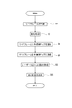
図2は、本実施形態に係る半導体装置の製造方法を示すフローチャート図である。
以下、図1(a)〜(c)及び図2を参照して説明する。
Next, a method for manufacturing the semiconductor device according to the present embodiment will be described.
FIG. 2 is a flowchart illustrating the method for manufacturing the semiconductor device according to the present embodiment.
Hereinafter, description will be made with reference to FIGS. 1 (a) to 1 (c) and FIG.
先ず、ステップS1に示すように、例えば、銅板をプレス加工することにより、リード11、コンタクト部19、リード部20及びゲートリード部24(以下、総称して「リードフレーム」という)を作製する。
次に、ステップS2に示すように、リード11及びコンタクト部19の表面に対して、粗化処理を施す。粗化処理は、例えば、酸性の薬液をリード11及びコンタクト部19に接触させることによって行う。酸性の薬液には、例えば、過酸化水素水及び硫酸の混合液を用いることができる。
First, as shown in Step S1, for example, a
Next, as shown in step S2, the surfaces of the
次に、ステップS3に示すように、緑色レーザーによるレーザー加工を行う。これにより、リード11のベッド部12の上面12aにおいて、半導体チップ15が接合される予定の領域を囲むように、例えば3本の溝29を形成する。上方から見て、各溝29の形状は矩形の枠状である。このとき、溝29の内面29aはレーザー光によって一旦溶融した後凝固するため、粗くなる。この結果、溝29の内面29aは上面12aにおける溝29を除く領域よりも粗くなる。また、リード11を形成する銅が熱酸化されることにより、溝29の内面29aには、不可避的に銅酸化膜29bが形成される。
Next, as shown in step S3, laser processing with a green laser is performed. Thereby, for example, three
次に、ステップS4に示すように、リード11のベッド部12の上面12aにおける溝29によって囲まれた領域にはんだ層16を形成する。はんだ層16は、例えば、固形はんだ、はんだペースト又は銀ペースト等によって形成する。次に、はんだ層16上に半導体チップ15を載置する。次に、半導体チップ15の上面の一部にはんだ層22を形成する。一方、リード部20の上面の一部にはんだ層21を形成する。次に、はんだ層21上及びはんだ層22上にコンタクト部19を載置する。
Next, as shown in step S4, the
次に、リード11、はんだ層16、半導体チップ15、はんだ層22、コンタクト部19、はんだ層21及びリード部20からなる構造体をリフロー炉に装入し、加熱してはんだ層16、21及び22を一旦溶融させて、その後、冷却して固化させる。これにより、半導体チップ15がはんだ層16を介してリード11に接合されると共に、はんだ層22を介してコンタクト部19に接合される。また、コンタクト部19がはんだ層21を介してリード部20に接合されて、リード18が形成される。
次に、ステップS5に示すように、ワイヤ25を介して、半導体チップ15のゲートパッド部23をゲートリード部24に接続する。
Next, a structure including the
Next, as shown in step S5, the
次に、ステップS6に示すように、液体状又は半固体状の樹脂材料によって半導体チップ15を覆う。このとき、樹脂材料は、半導体チップ15の他に、はんだ層16、リード11のベッド部12、リード部13におけるベッド部12側の部分、はんだ層22、コンタクト部19、はんだ層21、リード部20におけるコンタクト部19側の部分、ワイヤ25、及び、ゲートリード部24におけるリード11側の部分を覆うように配置する。次に、熱処理を行うことにより、樹脂材料を固化させる。これにより、封止部材27が形成される。
このようにして、本実施形態に係る半導体装置1が製造される。
Next, as shown in step S6, the
Thus, the
次に、本実施形態の効果について説明する。
本実施形態に係る半導体装置1においては、リード11と封止部材27との界面30において、この界面30が封止部材27の表面に達している境界30aとリード11における半導体チップ15が接合されている領域30bとの間に、溝29が形成されている。このため、界面30における境界30aと領域30bとの距離が長い。半導体装置1に印加される熱応力等の熱的、機械的、化学的ストレスにより、リード11と封止部材27との間に剥離が発生し、境界30aを起点として隙間が形成されても、境界30aと領域30bとの界面30に沿った実効的な距離が長いため、この隙間が界面30を伝わって領域30bまで到達しにくい。これにより、半導体装置1の信頼性を向上させることができる。
Next, effects of the present embodiment will be described.
In the
なお、隙間が界面30を伝わって領域30bまで到達すると、半導体装置1の製造工程において使用するフラックス及びめっき液等の薬液、並びに、外部環境に存在する水分等が、隙間を伝達してはんだ層16及び半導体チップ15に到達し、はんだ層16及び半導体チップ15を劣化させてしまう。例えば、半導体チップ15の電極(図示せず)を腐食させたり、リード11から溶出した銅を半導体チップ15の表面に析出させて電極間リークを発生させたりする。このため、半導体装置1の信頼性を確保するためには、できるだけリード11及び18と封止部材27との間に隙間が発生しないようにすること、及び、隙間が発生した場合でも、半導体チップ15等まで到達しないようにすることが効果的である。
When the gap reaches the
また、溝29をレーザー加工により形成することにより、上方から見て、ベッド部12の外縁と半導体チップ15との間の狭い領域に、溝29を精密に形成することができる。また、半導体装置1のサイズ、及び、リード11の厚さに応じて、溝29の幅及び深さを高精度に制御することができる。
In addition, by forming the
更に、半導体装置1においては、リード11の表面に粗化処理が施されているため、界面30における境界30aと領域30bとの実効的な距離が長くなる。これによっても、信頼性が向上する。同様に、リード18の表面にも粗化処理が施されているため、リード18と封止部材27との界面31の実効的な長さも長くなり、界面31を伝わって水分が進入することを抑制できる。
Further, in the
更にまた、半導体装置1においては、溝29内に封止部材27の一部が配置されている。このため、アンカー効果により、リード11と封止部材27との密着性が向上する。また、リード11及び18の表面に粗化処理が施されているため、これによっても、アンカー効果により、リード11及び18と封止部材27との密着性が向上する。この結果、半導体装置1の信頼性が向上する。
Furthermore, in the
更にまた、リード11及び18の表面に粗化処理が施されているため、リード11と封止部材27との界面30、又は、リード18と封止部材27との界面31に沿って隙間が形成され、この隙間内に水分が侵入した場合でも、水分の浸透圧が分散されて、水分が隙間の奥に侵入しにくくなる。これによっても、半導体装置1の信頼性が向上する。
Furthermore, since the surfaces of the
更にまた、溝29の内面29aに銅酸化膜29bが形成されているため、封止部材27を形成する樹脂の種類によっては、リード11と封止部材27との密着性をより一層向上させることができる。
Furthermore, since the
更にまた、本実施形態においては、封止部材27を形成する樹脂材料の母材として、例えば、ビフェニル系の樹脂材料又は多芳香環レジンを用いている。レーザー加工部や粗化処理部は酸化しやすく、また密着面も粗化されているため、一般的なオルクレゾールノボラックとフェノールノボラックからなるエポキシ樹脂では、粗化面への完全充填および金属面との反応が難しい場合がある。これに対して、ビフェニル等の低粘度かつOH基が多いベースレジンを用いることにより、密着性を向上させることができる。また、低吸水タイプの多芳香環レジンを使用し、樹脂材料にフィラーを含有させることにより、銅の酸化面との反応において、ミクロ的な水分の除去ポイントとなる。又は、ヘテロ系の密着性付与材を化学結合させることにより、密着力をより一層向上させることができる。
Furthermore, in the present embodiment, as a base material of the resin material forming the sealing
このように、本実施形態によれば、耐熱衝撃性、耐湿性及び耐薬品性が高く、信頼性が高い半導体装置を実現することができる。 As described above, according to the present embodiment, a highly reliable semiconductor device having high thermal shock resistance, moisture resistance, and chemical resistance can be realized.
(第2の実施形態)
次に、第2の実施形態について説明する。
図3は、本実施形態に係る半導体装置を示す平面図である。
(Second embodiment)
Next, a second embodiment will be described.
FIG. 3 is a plan view showing the semiconductor device according to the present embodiment.
図3に示すように、本実施形態に係る半導体装置2においては、溝29がその延伸方向に沿って複数の部分に分断されている。但し、溝29は、ベッド部12の上面12aにおけるリード部13と領域30bとの間には、必ず形成されている。
As shown in FIG. 3, in the semiconductor device 2 according to the present embodiment, the
本実施形態においては、溝29が分断されていることにより、はんだ層16が溝29まで到達した場合に、溶融したはんだが毛細管現象により溝29を伝わって、濡れ広がることを抑制できる。一般に、はんだは銅よりも樹脂材料に対する密着力が低いため、はんだの拡散を抑制することにより、密着性を確保することができる。一方、ベッド部12の上面12aにおけるリード部13と領域30bとの間には、溝29が形成されているため、リード部13の表面と封止部材27の表面とが接する境界30aから領域30bに向かう最短経路上には必ず溝29が介在することになり、隙間の伝播を抑制することができる。
本実施形態における上記以外の構成、製造方法及び効果は、前述の第1の実施形態と同様である。
In the present embodiment, since the
Other configurations, manufacturing methods, and effects of the present embodiment are the same as those of the above-described first embodiment.
(第3の実施形態)
次に、第3の実施形態について説明する。
図4(a)は本実施形態に係る半導体装置を示す平面図であり、(b)はその一部拡大断面図である。
(Third embodiment)
Next, a third embodiment will be described.
FIG. 4A is a plan view illustrating the semiconductor device according to the present embodiment, and FIG. 4B is a partially enlarged cross-sectional view thereof.
図4(a)及び(b)に示すように、本実施形態に係る半導体装置3においては、はんだ層16における溝29の直上域に相当する部分に、貫通部16aが形成されている。貫通部16aは溝29に連通されている。そして、貫通部16a及び溝29内には、封止部材27の一部が配置されている。
As shown in FIGS. 4A and 4B, in the
次に、本実施形態に係る半導体装置の製造方法について説明する。
図5は、本実施形態に係る半導体装置の製造方法を示すフローチャート図である。
図4(a)及び(b)、図5に示すように、本実施形態においては、ステップS1に示すように、リードフレーム(リード11、コンタクト部19、リード部20、ゲートリード部24)を作製し、ステップS2に示すように、リード11及びコンタクト部19に対して粗化処理を施す。
Next, a method for manufacturing the semiconductor device according to the present embodiment will be described.
FIG. 5 is a flowchart illustrating the method for manufacturing the semiconductor device according to the present embodiment.
As shown in FIGS. 4A and 4B and FIG. 5, in the present embodiment, as shown in step S1, the lead frame (lead 11,
次に、ステップS4に示すように、リード11及び18と半導体チップ15を接合する。このとき、はんだ層16が溝29を形成する予定の領域の一部まで流出するとする。次に、ステップS5に示すように、ゲートリード部24をワイヤ25を介して半導体チップ15のゲートパッド部23に接続する。
Next, as shown in step S4, the
次に、ステップS3に示すように、はんだ層16上からレーザー加工を施す。これにより、はんだ層16に貫通部16aが形成されると共に、リード11のベッド部12に溝29が形成される。溝29は、図4に示すように、延伸方向に沿って分断してもよく、分断しなくてもよい。
Next, as shown in step S3, laser processing is performed on the
次に、ステップS6に示すように、封止部材27を形成する。このとき、貫通部16a内及び溝29内にも封止部材27の一部が配置される。このようにして、本実施形態に係る半導体装置3が製造される。
Next, as shown in Step S6, the sealing
次に、本実施形態の効果について説明する。
本実施形態においては、封止部材27が貫通部16a内及び溝29内にも配置されている。これにより、アンカー効果によって、リード11及びはんだ層16と封止部材27との密着性が向上する。また、一般に、樹脂材料と銅との密着力は、樹脂材料とはんだとの密着力よりも強い。このため、封止部材27の一部を貫通部16aを介してベッド部12に接触させることにより、封止部材27とリード11との密着性がより一層向上する。
本実施形態における上記以外の構成、製造方法及び効果は、前述の第1の実施形態と同様である。
Next, effects of the present embodiment will be described.
In the present embodiment, the sealing
Other configurations, manufacturing methods, and effects of the present embodiment are the same as those of the above-described first embodiment.
(第4の実施形態)
次に、第4の実施形態について説明する。
図6(a)は、本実施形態に係る半導体装置を示す平面図であり、(b)はその断面図であり、(c)は(b)の領域Aを示す一部拡大断面図である。
(Fourth embodiment)
Next, a fourth embodiment will be described.
6A is a plan view showing the semiconductor device according to the present embodiment, FIG. 6B is a cross-sectional view thereof, and FIG. 6C is a partially enlarged cross-sectional view showing a region A of FIG. .
図6(a)〜(c)に示すように、本実施形態に係る半導体装置4においては、溝29内及び溝29上の一部に、エンキャップ材35が設けられている。エンキャップ材35においては、溝29内に配置された部分35aと、3本の溝29上にわたって配置された半球状の部分35bとが設けられている。
As shown in FIGS. 6A to 6C, in the semiconductor device 4 according to the present embodiment, an
エンキャップ材35は、封止部材27を形成する樹脂材料とは異なる樹脂材料によって形成されており、例えば、リード11及び封止部材27の双方に対して良好な密着性をもつ樹脂材料によって形成されており、例えば、応力が低い樹脂材料、又は、OH基が多く金属との密着性が良好な樹脂材料によって形成されている。
The
次に、本実施形態に係る半導体装置の製造方法について説明する。
図7は、本実施形態に係る半導体装置の製造方法を示すフローチャート図である。
Next, a method for manufacturing the semiconductor device according to the present embodiment will be described.
FIG. 7 is a flowchart illustrating the method for manufacturing the semiconductor device according to the present embodiment.
図6(a)〜(c)及び図7に示すように、本実施形態においては、前述の第1の実施形態と同様な方法により、ステップS1に示すリードフレームの作製、ステップS2に示す粗化処理、ステップS3に示すレーザー加工を実施する。 As shown in FIGS. 6A to 6C and FIG. 7, in this embodiment, the lead frame shown in step S1 is manufactured and the rough frame shown in step S2 is manufactured by the same method as in the first embodiment. The laser processing shown in step S3 is performed.
次に、ステップS7に示すように、液体状の樹脂材料を溝29上に滴下して、溝29に沿って流通させる。その後、この樹脂材料を固化させる。これにより、溝29内及び溝29上の一部に、エンキャップ材35が形成される。
Next, as shown in step S7, a liquid resin material is dropped on the
次に、前述の第1の実施形態と同様な方法により、ステップS4に示すリード11及び18と半導体チップ15の接合、ステップS5に示す半導体チップ15とゲートリード部24との接続、ステップS6に示す封止部材27の形成を実施する。これにより、本実施形態に係る半導体装置4が製造される。
Next, by the same method as in the above-described first embodiment, bonding of the
次に、本実施形態の効果について説明する。
本実施形態によれば、ステップS7に示す工程において溝29内にエンキャップ材35を埋め込んだ後、ステップS4に示す工程においてはんだ層16を溶融させているため、はんだが毛細管現象によって溝29内を流動することを防止できる。
Next, effects of the present embodiment will be described.
According to the present embodiment, the
また、リード11及び封止部材27の双方に対して良好な密着性をもつ樹脂材料によってエンキャップ材35を形成することにより、リード11と封止部材27がエンキャップ材35を介してより強固に結合される。この結果、リード11と封止部材27との間に隙間が形成されにくくなり、半導体装置の信頼性がより向上する。
本実施形態における上記以外の構成、製造方法及び効果は、前述の第1の実施形態と同様である。
In addition, by forming the encapsulating
Other configurations, manufacturing methods, and effects of the present embodiment are the same as those of the above-described first embodiment.
(第5の実施形態)
次に、第5の実施形態について説明する。
図8は、本実施形態に係る半導体装置の製造方法を示すフローチャート図である。
(Fifth embodiment)
Next, a fifth embodiment will be described.
FIG. 8 is a flowchart illustrating the method for manufacturing the semiconductor device according to the present embodiment.
図8に示すように、本実施形態は、前述の第1の実施形態(図2参照)と比較して、レーザー加工と粗化処理の順番が異なっている。すなわち、図8に示すように、本実施形態においては、ステップS3に示すレーザー加工を行った後、ステップS2に示す粗化処理を行う。これにより、レーザー加工によって生じた金属異物が、粗化処理において使用する薬液によって除去される。この結果、金属異物を介した電流のリーク等の不具合を防止することができ、半導体装置の信頼性がより一層向上する。 As shown in FIG. 8, the present embodiment is different from the first embodiment (see FIG. 2) in the order of laser processing and roughening processing. That is, as shown in FIG. 8, in the present embodiment, after performing the laser processing shown in step S3, the roughening processing shown in step S2 is performed. Thereby, the metallic foreign matter generated by the laser processing is removed by the chemical used in the roughening treatment. As a result, it is possible to prevent a problem such as a current leak through a metal foreign matter, and to further improve the reliability of the semiconductor device.
また、レーザー加工によって形成された銅酸化膜29bが、粗化処理のための薬液処理によって除去される。これにより、封止部材27を形成する樹脂材料の種類によっては、封止部材27とリード11との密着力が向上する。
Further, the
(第6の実施形態)
次に、第6の実施形態について説明する。
図9は、本実施形態に係る半導体装置の製造方法を示すフローチャート図である。
(Sixth embodiment)
Next, a sixth embodiment will be described.
FIG. 9 is a flowchart illustrating the method for manufacturing the semiconductor device according to the present embodiment.
図9に示すように、本実施形態においては、前述の第5の実施形態と同様に、ステップS1、S3、S2、S4、S5に示す工程を実施した後、ステップS8に示すように、二度目のレーザー処理を行う。このレーザー処理において、レーザーが照射された部分は、例えば500℃以上の温度に加熱される。このため、はんだペースト、銀ペースト、はんだに添加する仮固定剤等から発生する残渣物を熱分解することができる。この結果、残渣物に起因した密着性の低下を阻止できる。
本実施形態における上記以外の構成、製造方法及び効果は、前述の第1の実施形態と同様である。
As shown in FIG. 9, in the present embodiment, as in the above-described fifth embodiment, after performing the processes shown in steps S1, S3, S2, S4, and S5, as shown in step S8, A second laser treatment is performed. In this laser treatment, the portion irradiated with the laser is heated to, for example, a temperature of 500 ° C. or more. Therefore, residues generated from the solder paste, the silver paste, the temporary fixing agent added to the solder, and the like can be thermally decomposed. As a result, a decrease in adhesion due to the residue can be prevented.
Other configurations, manufacturing methods, and effects of the present embodiment are the same as those of the above-described first embodiment.
以上説明した実施形態によれば、信頼性が高い半導体装置及びその製造方法を実現することができる。 According to the embodiment described above, a highly reliable semiconductor device and a method for manufacturing the same can be realized.
以上、本発明のいくつかの実施形態を説明したが、これらの実施形態は、例として提示したものであり、発明の範囲を限定することは意図していない。これら新規な実施形態は、その他の様々な形態で実施されることが可能であり、発明の要旨を逸脱しない範囲で、種々の省略、置き換え、変更を行うことができる。これら実施形態やその変形は、発明の範囲や要旨に含まれるとともに、特許請求の範囲に記載された発明及びその等価物の範囲に含まれる。また、前述の実施形態は、相互に組み合わせて実施することもできる。 While some embodiments of the present invention have been described above, these embodiments have been presented by way of example only, and are not intended to limit the scope of the inventions. These new embodiments can be implemented in other various forms, and various omissions, replacements, and changes can be made without departing from the spirit of the invention. These embodiments and modifications thereof are included in the scope and gist of the invention, and are also included in the scope of the invention described in the claims and the equivalents thereof. Further, the above-described embodiments can be implemented in combination with each other.
1、2、3、4:半導体装置、11:リード、12:ベッド部、12a:上面、13:リード部、15:半導体チップ、15a:上面、16:はんだ層、16a:貫通部、18:リード、19:コンタクト部、20:リード部、21:はんだ層、22:はんだ層、23:ゲートパッド部、24:ゲートリード部、25:ワイヤ、27:封止部材、29:溝、29a:内面、29b:銅酸化膜、30:界面、30a:境界、30b:領域、31:界面、35:エンキャップ材、35a、35b:部分、A:領域 1, 2, 3, 4: semiconductor device, 11: lead, 12: bed portion, 12a: upper surface, 13: lead portion, 15: semiconductor chip, 15a: upper surface, 16: solder layer, 16a: penetrating portion, 18: Lead, 19: Contact, 20: Lead, 21: Solder layer, 22: Solder layer, 23: Gate pad, 24: Gate lead, 25: Wire, 27: Sealing member, 29: Groove, 29a: Inner surface, 29b: Copper oxide film, 30: Interface, 30a: Boundary, 30b: Region, 31: Interface, 35: Encap material, 35a, 35b: Part, A: Region
Claims (7)
前記ベッド部の上面の一部に接合された半導体チップと、
前記半導体チップの上面に接合されたコンタクト部と、
前記コンタクト部に電気的に接続された第2リード部と、
樹脂材料からなり、前記第1リード部の一部、前記ベッド部、前記半導体チップ、前記コンタクト部、及び、前記第2リード部の一部を覆う封止部材と、
前記ベッド部と前記半導体チップとの間に設けられたはんだ層と、
を備え、
前記ベッド部の前記上面における前記封止部材に覆われた領域には、前記半導体チップが接合された領域を囲む溝が形成され、
前記はんだ層における前記溝の直上域には貫通部が形成されており、
前記封止部材の一部は前記貫通部内に配置された半導体装置。 A bed portion from which the first lead portion projects,
A semiconductor chip joined to a part of the upper surface of the bed portion,
A contact portion joined to the upper surface of the semiconductor chip,
A second lead portion electrically connected to the contact portion;
A sealing member made of a resin material and covering a part of the first lead part, the bed part, the semiconductor chip, the contact part, and a part of the second lead part;
A solder layer provided between the bed and the semiconductor chip,
With
In a region of the upper surface of the bed portion covered with the sealing member, a groove surrounding a region where the semiconductor chip is bonded is formed ,
A penetrating portion is formed in a region immediately above the groove in the solder layer,
A semiconductor device in which a part of the sealing member is disposed in the through portion .
前記溝は、少なくとも、前記ベッド部の前記上面における前記半導体チップが接合された前記領域と前記第1リード部との間に形成されている請求項1記載の半導体装置。 The groove is divided along a direction in which the groove extends,
2. The semiconductor device according to claim 1, wherein the groove is formed at least between the region where the semiconductor chip is bonded on the upper surface of the bed portion and the first lead portion. 3.
前記ベッド部の上面の一部に、はんだ層を介して半導体チップを接合する工程と、
前記半導体チップの上面にコンタクト部を接合する工程と、
前記ベッド部の前記上面における前記半導体チップが接合された領域の周囲に、緑色レーザーを用いたレーザー加工により、前記はんだ層を介して溝を形成する工程と、
樹脂材料により、前記ベッド部より延伸する第1リード部の一部、前記ベッド部、前記半導体チップ、前記コンタクト部、及び、前記コンタクト部に電気的に接続された第2リード部の一部を覆う封止部材を形成する工程と、
を備えた半導体装置の製造方法。 A step of roughening the surface of the bed portion containing copper,
Bonding a semiconductor chip to a part of the upper surface of the bed portion via a solder layer,
Bonding a contact portion to the upper surface of the semiconductor chip,
A step of forming a groove through the solder layer by laser processing using a green laser around a region where the semiconductor chip on the upper surface of the bed portion is joined,
A portion of the first lead extending from the bed, a portion of the bed, the semiconductor chip, the contact, and a portion of the second lead electrically connected to the contact are formed of a resin material. Forming a sealing member to cover;
A method for manufacturing a semiconductor device comprising:
Priority Applications (1)
| Application Number | Priority Date | Filing Date | Title |
|---|---|---|---|
| JP2017059873A JP6636978B2 (en) | 2017-03-24 | 2017-03-24 | Semiconductor device and manufacturing method thereof |
Applications Claiming Priority (1)
| Application Number | Priority Date | Filing Date | Title |
|---|---|---|---|
| JP2017059873A JP6636978B2 (en) | 2017-03-24 | 2017-03-24 | Semiconductor device and manufacturing method thereof |
Publications (3)
| Publication Number | Publication Date |
|---|---|
| JP2018163962A JP2018163962A (en) | 2018-10-18 |
| JP2018163962A5 JP2018163962A5 (en) | 2019-01-17 |
| JP6636978B2 true JP6636978B2 (en) | 2020-01-29 |
Family
ID=63860368
Family Applications (1)
| Application Number | Title | Priority Date | Filing Date |
|---|---|---|---|
| JP2017059873A Expired - Fee Related JP6636978B2 (en) | 2017-03-24 | 2017-03-24 | Semiconductor device and manufacturing method thereof |
Country Status (1)
| Country | Link |
|---|---|
| JP (1) | JP6636978B2 (en) |
Families Citing this family (2)
| Publication number | Priority date | Publication date | Assignee | Title |
|---|---|---|---|---|
| JP2021174883A (en) * | 2020-04-24 | 2021-11-01 | Jx金属株式会社 | Metal plate, metal resin composite body and semiconductor device |
| JP7474213B2 (en) * | 2021-03-16 | 2024-04-24 | 株式会社東芝 | Semiconductor Device |
Family Cites Families (8)
| Publication number | Priority date | Publication date | Assignee | Title |
|---|---|---|---|---|
| JP3065045B2 (en) * | 1998-11-13 | 2000-07-12 | 日本電気株式会社 | Semiconductor device |
| JP2001077264A (en) * | 1999-09-01 | 2001-03-23 | Matsushita Electronics Industry Corp | Manufacture of resin sealed semiconductor device |
| JP4591362B2 (en) * | 2006-01-25 | 2010-12-01 | 株式会社デンソー | Manufacturing method of electronic device |
| JP5745238B2 (en) * | 2010-07-30 | 2015-07-08 | セミコンダクター・コンポーネンツ・インダストリーズ・リミテッド・ライアビリティ・カンパニー | Semiconductor device and manufacturing method thereof |
| JP2014007363A (en) * | 2012-06-27 | 2014-01-16 | Renesas Electronics Corp | Method of manufacturing semiconductor device and semiconductor device |
| JP2016029676A (en) * | 2012-12-19 | 2016-03-03 | 富士電機株式会社 | Semiconductor device |
| JP2016058612A (en) * | 2014-09-11 | 2016-04-21 | 株式会社デンソー | Semiconductor device |
| JP6468085B2 (en) * | 2015-06-11 | 2019-02-13 | 株式会社デンソー | Substrate and manufacturing method thereof |
-
2017
- 2017-03-24 JP JP2017059873A patent/JP6636978B2/en not_active Expired - Fee Related
Also Published As
| Publication number | Publication date |
|---|---|
| JP2018163962A (en) | 2018-10-18 |
Similar Documents
| Publication | Publication Date | Title |
|---|---|---|
| JP4846515B2 (en) | Optical semiconductor device and method for manufacturing optical semiconductor device | |
| JP6206494B2 (en) | Semiconductor device | |
| JP2010123686A (en) | Semiconductor device and manufacturing method thereof | |
| US20160300779A1 (en) | Semiconductor package and manufacturing method thereof | |
| US8008773B2 (en) | Semiconductor device and method for fabricating semiconductor device | |
| JP4967277B2 (en) | Semiconductor device and manufacturing method thereof | |
| CN103003965B (en) | For semiconductor chip the bogey with the solder flux stop part of the compacted stream of anti-solder flux, there is the electronic device of bogey and there is the opto-electronic device of bogey | |
| JP6636978B2 (en) | Semiconductor device and manufacturing method thereof | |
| US20150262917A1 (en) | Semiconductor device and method of manufacturing the same | |
| JP5732880B2 (en) | Semiconductor device and manufacturing method thereof | |
| JP2015103713A (en) | Semiconductor device | |
| JP5233853B2 (en) | Semiconductor device | |
| US20140291831A1 (en) | Semiconductor device and manufacturing method for semiconductor device | |
| US20150048504A1 (en) | Package assembly for chip and method of manufacturing same | |
| JP5579148B2 (en) | Power semiconductor device | |
| JP6381489B2 (en) | Manufacturing method of semiconductor device | |
| JP6863819B2 (en) | Lead frame and its manufacturing method | |
| JP2015144199A (en) | semiconductor device | |
| JP6477105B2 (en) | Semiconductor device | |
| JP5734493B2 (en) | Power semiconductor device | |
| JP4137981B2 (en) | Manufacturing method of semiconductor device | |
| JP4861200B2 (en) | Power module | |
| JP6119553B2 (en) | Power semiconductor device and manufacturing method thereof | |
| JP2012195546A (en) | Semiconductor device, and packaging body and manufacturing method of the same | |
| US12080621B2 (en) | Semiconductor device and method of manufacturing semiconductor device |
Legal Events
| Date | Code | Title | Description |
|---|---|---|---|
| A711 | Notification of change in applicant |
Free format text: JAPANESE INTERMEDIATE CODE: A712 Effective date: 20170911 |
|
| A711 | Notification of change in applicant |
Free format text: JAPANESE INTERMEDIATE CODE: A711 Effective date: 20170912 |
|
| A521 | Request for written amendment filed |
Free format text: JAPANESE INTERMEDIATE CODE: A523 Effective date: 20171031 |
|
| A521 | Request for written amendment filed |
Free format text: JAPANESE INTERMEDIATE CODE: A523 Effective date: 20181130 |
|
| A621 | Written request for application examination |
Free format text: JAPANESE INTERMEDIATE CODE: A621 Effective date: 20181130 |
|
| A977 | Report on retrieval |
Free format text: JAPANESE INTERMEDIATE CODE: A971007 Effective date: 20190725 |
|
| A131 | Notification of reasons for refusal |
Free format text: JAPANESE INTERMEDIATE CODE: A131 Effective date: 20190819 |
|
| A521 | Request for written amendment filed |
Free format text: JAPANESE INTERMEDIATE CODE: A523 Effective date: 20191003 |
|
| TRDD | Decision of grant or rejection written | ||
| A01 | Written decision to grant a patent or to grant a registration (utility model) |
Free format text: JAPANESE INTERMEDIATE CODE: A01 Effective date: 20191120 |
|
| A61 | First payment of annual fees (during grant procedure) |
Free format text: JAPANESE INTERMEDIATE CODE: A61 Effective date: 20191219 |
|
| R150 | Certificate of patent or registration of utility model |
Ref document number: 6636978 Country of ref document: JP Free format text: JAPANESE INTERMEDIATE CODE: R150 |
|
| LAPS | Cancellation because of no payment of annual fees |