JP6620313B2 - Host device, slave device and removable system - Google Patents
Host device, slave device and removable system Download PDFInfo
- Publication number
- JP6620313B2 JP6620313B2 JP2016234662A JP2016234662A JP6620313B2 JP 6620313 B2 JP6620313 B2 JP 6620313B2 JP 2016234662 A JP2016234662 A JP 2016234662A JP 2016234662 A JP2016234662 A JP 2016234662A JP 6620313 B2 JP6620313 B2 JP 6620313B2
- Authority
- JP
- Japan
- Prior art keywords
- signal
- voltage level
- signal line
- slave device
- line
- Prior art date
- Legal status (The legal status is an assumption and is not a legal conclusion. Google has not performed a legal analysis and makes no representation as to the accuracy of the status listed.)
- Active
Links
Images


Description
本開示は、相互に接続が可能なホスト装置及びスレーブ装置、さらにホスト装置及びスレーブ装置から構成されるリムーバブルシステムに関する。 The present disclosure relates to a host device and a slave device that can be connected to each other, and a removable system that includes the host device and the slave device.
近年、フラッシュメモリ等の大容量の不揮発性記憶素子を備え、高速でのデータ処理が可能な、例えばカード形状のSDカード、メモリースティックといったスレーブ装置が市場に普及している。このようなスレーブ装置は、スレーブ装置を使用可能なホスト装置である、パーソナルコンピュータ、スマートフォン、デジタルカメラ、オーディオプレーヤ及びカーナビゲーションシステム等において、利用されている。 In recent years, slave devices such as a card-shaped SD card and a memory stick, which have a large-capacity non-volatile storage element such as a flash memory and can process data at high speed, have spread in the market. Such slave devices are used in personal computers, smartphones, digital cameras, audio players, car navigation systems, and the like, which are host devices that can use the slave devices.
例えば、特許文献1は、ホスト装置及びスレーブ装置を使用した通信システムにおいて、複数のインターフェイス電圧から動作電圧を選択する技術を開示している。
For example,
また、特許文献2は、電源がONであるかOFFであるかの状態、及び特定の信号線がハイレベルであるかローレベルであるかの状態に応じて、電子装置(スレーブ装置)で使用するインターフェイス回路を決定する技術を開示している。
ホスト装置及びスレーブ装置を使用した通信システムにおいて、インターフェイス処理速度を向上させるためには、最大インターフェイス電圧を低減させることが有効である。更に昨今、半導体プロセスの微細化に伴って、特にホスト装置においてより低い最大インターフェイス電圧に限った半導体装置を導入したいという要望が高まっている。一方、市場で普及している既存のインターフェイスを継続して活用できるようインターフェイスの互換性を保つことも要望されている。すなわち、スレーブ装置、及びスレーブ装置をホスト装置と接続させるためにホスト装着に実装するスロットの形状、端子の位置、大きさ等を、従来のものと同様のままとしておくことが要望されている。 In a communication system using a host device and a slave device, it is effective to reduce the maximum interface voltage in order to improve the interface processing speed. Furthermore, with the recent miniaturization of semiconductor processes, there is an increasing demand to introduce a semiconductor device limited to a lower maximum interface voltage especially in a host device. On the other hand, there is also a demand for maintaining interface compatibility so that existing interfaces that are popular in the market can be used continuously. That is, there is a demand for the slave device and the shape of the slot to be mounted on the host to connect the slave device to the host device, the position of the terminal, the size, etc. remain the same as the conventional one.
これらを同時に満たそうとした場合、既存のインターフェイスによるホスト装置に対して、既存よりも相対的に低い最大インターフェイス電圧に対応した新規インターフェイスによるスレーブ装置が誤って装着される可能性がある。同様に、既存よりも相対的に低い最大インターフェイス電圧に対応した新規インターフェイスによるホスト装置に対して、既存のインターフェイスによるスレーブ装置が誤って装着される可能性がある。そして、新規のインターフェイス側の装置が、既存のインターフェイス側の装置による相対的に高い最大インターフェイス電圧により破壊されてしまう可能性がある。 When trying to satisfy these simultaneously, there is a possibility that a slave device with a new interface corresponding to the maximum interface voltage that is relatively lower than that of the existing interface is erroneously attached to the host device with the existing interface. Similarly, a slave device with an existing interface may be erroneously attached to a host device with a new interface corresponding to a maximum interface voltage that is relatively lower than the existing one. Then, there is a possibility that the new interface-side device is destroyed by the relatively high maximum interface voltage of the existing interface-side device.
本開示は、上記課題に鑑みてなされたものであり、インターフェイスの互換性を保つと同時に、シングルエンド方式の最大インターフェイス電圧を低減させたとしても、安全に使用することができるホスト装置、スレーブ装置、及びリムーバブルシステムを提供する。 The present disclosure has been made in view of the above problems, and can maintain a compatible interface, and at the same time, can reduce the maximum interface voltage of a single-ended system and can be used safely. And a removable system.
本開示は、最大電圧レベルの異なる複数のインターフェイスでスレーブ装置と接続されうるホスト装置であって、スレーブ装置に対して電源を供給し、第1の信号線を介して第1電圧レベルである1.8Vの信号、第2電圧レベルである0Vの信号を順に送信する。その後、第2の信号線を介して第1電圧レベルである1.8Vの信号を受信したとき、スレーブ装置との通信を開始することを特徴とする。
The present disclosure is a host device that can be connected to a slave device through a plurality of interfaces having different maximum voltage levels, supplies power to the slave device, and is a
また、本開示は、最大電圧レベルの異なる複数のインターフェイスでホスト装置と接続されうるスレーブ装置であって、ホスト装置より電源を供給され、かつ第1の信号線を介して第1電圧レベルである1.8Vの信号、第2電圧レベルである0Vの信号を順に受信したとき、第2の信号線を介して第1電圧レベルである1.8Vの信号を送信し、その後、第1の信号線を介して第1電圧レベルである1.8Vの信号を受信したとき、第2の信号線を介した第1電圧レベルである1.8Vの信号の送信を停止することを特徴とする。 In addition, the present disclosure is a slave device that can be connected to a host device through a plurality of interfaces having different maximum voltage levels, is supplied with power from the host device, and is at the first voltage level via the first signal line. When a signal of 1.8V and a signal of 0V that is the second voltage level are sequentially received, a signal of 1.8V that is the first voltage level is transmitted via the second signal line, and then the first signal is transmitted. When a signal of 1.8V that is the first voltage level is received via the line, transmission of the signal of 1.8V that is the first voltage level via the second signal line is stopped.
また、本開示は、上記ホスト装置及びスレーブ装置から構成されるリムーバブルシステムを含む。 The present disclosure also includes a removable system that includes the host device and the slave device.
本開示により、最大信号電圧を低減させたシングルエンド方式インターフェイスを導入した場合にも、インターフェイスの互換性を保つと同時に、安全に使用することができるホスト装置、スレーブ装置及びリムーバブルシステムを提供できる。 According to the present disclosure, it is possible to provide a host device, a slave device, and a removable system that can maintain interface compatibility and can be used safely even when a single-ended interface having a reduced maximum signal voltage is introduced.
以下、適宜図面を参照しながら、実施の形態を詳細に説明する。但し、必要以上に詳細な説明は省略する場合がある。例えば、既によく知られた事項の詳細説明や実質的に同一の構成に対する重複説明を省略する場合がある。これは、以下の説明が不必要に冗長になるのを避け、当業者の理解を容易にするためである。 Hereinafter, embodiments will be described in detail with reference to the drawings as appropriate. However, more detailed explanation than necessary may be omitted. For example, detailed descriptions of already well-known matters and repeated descriptions for substantially the same configuration may be omitted. This is to avoid the following description from becoming unnecessarily redundant and to facilitate understanding by those skilled in the art.
なお、本開示は、当業者が理解するための添付図面及び以下の説明を提供するのであって、これらによって請求の範囲に記載の主題を限定することを意図するものではない。 It should be noted that the present disclosure provides the accompanying drawings and the following description for understanding by those skilled in the art, and is not intended to limit the claimed subject matter.
[1.本開示にかかるリムーバブルシステムが解決しようとする課題について]
最初に、本開示にかかるリムーバブルシステムが解決しようとする課題について、図1から図6を用いて説明する。なお、以後インターフェイスのことを適宜I/Fと略記する。
[1. Issues to be solved by the removable system according to the present disclosure]
First, problems to be solved by the removable system according to the present disclosure will be described with reference to FIGS. 1 to 6. Hereinafter, the interface is abbreviated as I / F as appropriate.
[1−1.レガシーホスト装置及び、レガシースレーブ装置の構成]
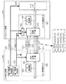
図1は、従来のシングルエンドI/F(以後レガシーI/Fと記す)に対応したレガシーホスト装置100に抜き差し可能なレガシースレーブ装置120が接続されたリムーバブルシステムの構成について説明したブロック図である。図1に示すように、レガシーホスト装置100は、少なくとも電源供給部101、レガシーI/F半導体チップ102を備えている。そして、レガシーI/F半導体チップ102は、少なくともレギュレータ103、2つの電源入力のうち一方を選択する電気的スイッチであるSW104、ホスト装置I/F部105、I/F制御部106を備えている。なお、レギュレータ103は、レガシーI/F半導体チップ102の外部に配置することも可能である。
[1-1. Configuration of Legacy Host Device and Legacy Slave Device]
FIG. 1 is a block diagram illustrating a configuration of a removable system in which a
レガシーホスト装置100と、レガシースレーブ装置120とは、機械的に接続される。また、レガシーホスト装置100は、3.3V電源ラインであるVDD1ライン110を介して、レガシースレーブ装置120と電気的に接続される。
The
レガシースレーブ装置120は、少なくともレガシーI/F半導体チップ121、バックエンドモジュール126を備えている。なお、バックエンドモジュール126は、フラッシュメモリのような記録媒体や無線通信モジュールのようなデバイスを指す。そして、レガシーI/F半導体チップ121は、少なくともレギュレータ122、SW123、スレーブ装置I/F部124、I/F制御部125を備えている。なお、レギュレータ122は、レガシーI/F半導体チップ121の外部に配置することも可能である。
The
ホスト装置I/F部105と、スレーブ装置I/F部124とは、CLKライン111、CMDライン112、DATライン113を介して、信号通信を行う。なお、DATライン113は、DAT0ライン113a、DAT1ライン113b、DAT2ライン113c、DAT3ライン113dの4本の信号線からなる。
The host device I /
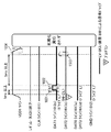
図2は、レガシーホスト装置100及びレガシースレーブ装置120における、電源起動後のルーチンについて説明した図である。また、図3は、2種類のレガシースレーブ装置120(詳細は後述)におけるコマンドとレスポンスの詳細を説明した図である。
FIG. 2 is a diagram illustrating a routine after power activation in the
[1−2.レガシーホスト装置及び、レガシースレーブ装置の詳細動作]
以下、図1から図3を用いて、レガシーホスト装置100にレガシースレーブ装置120が接続されたときの動作について説明する。
[1-2. Detailed operation of legacy host device and legacy slave device]
Hereinafter, an operation when the
電源起動時、レガシーホスト装置100の電源供給部101から3.3V電源が、レガシーI/F半導体チップ102、レギュレータ103、SW104にVDD1ライン110を介してレガシースレーブ装置120に供給される。
At the time of power activation, 3.3 V power is supplied from the
レガシーI/F半導体チップ102は、電源供給部101から供給された3.3V電源を、レガシーI/F半導体チップ102内に配置されたあらゆるモジュールに供給して、各モジュールが動作可能な状態とする。
The legacy I /
レギュレータ103は、供給された電源の電圧をI/F制御部106の指示により適宜変換して出力する装置である。図1から図3における形態では、レギュレータ103により電源供給部101から供給される3.3V電源が1.8V電源に変換される。
The
SW104は、電源供給部101から供給される3.3V電源と、レギュレータ103から供給される1.8V電源のいずれか一方を選択して、ホスト装置I/F部105に供給する。図1から図3における形態では、電源起動直後は、3.3V電源をホスト装置I/F部105に供給する。これにより、ホスト装置I/F部105から出力されるCLKライン111、CMDライン112、及びDATライン113の信号電圧は3.3Vとなる。
The
一方、VDD1ライン110を介してレガシースレーブ装置120に供給された3.3V電源は、レガシーI/F半導体チップ121、レギュレータ122、SW123、及びバックエンドモジュール126に供給される。
On the other hand, the 3.3 V power supplied to the
レガシーI/F半導体チップ121は、供給された3.3V電源を、レガシーI/F半導体チップ121内に配置されたあらゆるモジュールに供給して、各モジュールが動作可能な状態とする。また、レギュレータ122によりVDD1ライン110を介して供給された3.3V電源は1.8V電源に変換される。また、電源起動直後、SW123は3.3V電源をスレーブ装置I/F部124に供給する。
The legacy I /
スレーブ装置I/F部124に供給された3.3V電源により、スレーブ装置I/F部124から出力されるCMDライン112、及びDATライン113の信号電圧は3.3Vとなる。
Due to the 3.3V power supply supplied to the slave device I /
レガシーホスト装置100のホスト装置I/F部105は、CLKライン111、CMDライン112、及び4本のDATライン113によりレガシースレーブ装置120のスレーブ装置I/F部124と接続されている。CLKライン111上において、シングルエンド方式のクロック信号は、レガシーホスト装置100からレガシースレーブ装置120へ伝送される。CMDライン112は、レガシーホスト装置100がレガシースレーブ装置120を制御するためのコマンド、及び各コマンドに対応するレスポンスが3.3V信号のシングルエンド方式により伝送される。例えば、コマンドは、レガシーホスト装置100がレガシースレーブ装置120に送信し、レスポンスは、レガシースレーブ装置120がレガシーホスト装置100に送信する。そのため、CMDライン112は双方向通信である。
The host device I /
一方、DATライン113は、主として静止画やテキストなどのデータコンテンツを高速に伝送する信号線であり、4本の信号線より成り立っている。信号線の構成は、CMDライン112と同様である。
On the other hand, the
レガシーホスト装置100は、レガシースレーブ装置120が装着されていない状態で各信号線がフローティング状態になることを回避するため、CMDライン112、及びすべてのDATライン113を、図示していないプルアップ抵抗で、所定の電圧(通常3.3V)にプルアップする。さらに、起動直後、レガシーホスト装置100は、レガシースレーブ装置120において、図示していないプルアップ抵抗により、DAT3ライン113dとVDD1ライン110とを接続する。これは、起動直後、レガシーホスト装置100がレガシースレーブ装置120に接続されているかの検知に利用できるものである。
In the
また、電源起動時、レガシーホスト装置100は、通常CMDライン112、及びDATライン113の各端子をローレベル、ハイレベルいずれにもドライブせず、入力状態、すなわちハイインピーダンス(Hi−Z;解放)状態とする。従って、これらの信号線は、レガシーホスト装置100がドライブしない限り、VDD1の印加に伴って前述のプルアップ抵抗によりハイレベルに遷移する(200)。
Further, when the power is turned on, the
なお、本明細書において、信号がローレベルであるとは、信号の電圧が0V及びその近傍にある状態であることをいい、通常0を意味する。一方信号がハイレベルであるとは、信号の電圧がローレベルより高く、かつローレベルの信号と容易に識別が可能な状態であることをいい、通常1を意味する。なお、ハイレベルは、3.3Vの高電圧信号(以下3.3V信号と称する)の場合と、1.8Vの低電圧信号(以下1.8V信号と称する)の場合とでは、絶対的な電圧の値は異なる。 In this specification, the signal being at a low level means that the voltage of the signal is 0 V and in the vicinity thereof, and usually means 0. On the other hand, a signal having a high level means that the voltage of the signal is higher than a low level and is easily distinguishable from a low level signal, and usually means 1. The high level is absolute in the case of a 3.3V high voltage signal (hereinafter referred to as 3.3V signal) and in the case of a 1.8V low voltage signal (hereinafter referred to as 1.8V signal). The voltage value is different.
電源起動後、ホスト装置I/F部105は、SW104を介して電源供給部101から供給される3.3V(高電圧)電源により、3.3V信号のシングルエンド方式のクロックを生成する。そして、電源供給部101からの電源出力が3.3Vに安定してから1ms以上経過した後、クロックをスレーブ装置I/F部124に供給する(201)。
After power activation, the host device I /
その後、レガシーホスト装置100は、接続されたレガシースレーブ装置120の特性確認及び初期化を行う初期化ルーチンに入る。ホスト装置I/F部105は、最初にリセットコマンド202を発行する。なお、リセットコマンドに対応するレスポンスは、存在しない。
Thereafter, the
続いて、レガシーホスト装置100は、接続されたスレーブ装置のI/F条件(例えば対応電源電圧など)をチェックするためのコマンドであるI/F条件チェックコマンド203aをI/F制御部106で生成し、CMDライン112を介してスレーブ装置I/F部124に送信する。
Subsequently, the
I/F条件チェックコマンド203aは、スレーブ装置I/F部124を介して、I/F制御部125に送信される。I/F制御部125は、コマンドの内容を解釈し、対応するレスポンス203bを生成し、CMDライン112を介してレガシーホスト装置100に返送する。
The I / F
続いて、レガシーホスト装置100は、初期化コマンド204aをレガシースレーブ装置120にCMDライン112を介して送信する。I/F条件チェックコマンド203aの場合と同様、レガシースレーブ装置120は、コマンドの内容を解釈し、対応するレスポンス204bを生成し、CMDライン112を介してレガシーホスト装置100に返送する。
Subsequently, the
その後、詳述はしないが所定の初期化プロセスを経て、レガシーホスト装置100は、Writeコマンド205aを発行する。このとき、レガシーホスト装置100は、レガシースレーブ装置120から送信されるレスポンス205bを受信後、レガシースレーブ装置120のバックエンドモジュール126に書き込むデータ205cを、DATライン113を介して送信する。
Thereafter, though not described in detail, the
さて、レガシーI/Fには、非UHS−I及びUHS−Iの2種類のI/Fが存在する。非UHS−Iは、CLKライン111、CMDライン112、DATライン113の信号電圧が終始3.3V信号のI/Fである。一方、UHS−Iは、電源起動直後は3.3V信号を用い、途中で1.8V信号に切り換える。
In the legacy I / F, there are two types of I / Fs, non-UHS-I and UHS-I. In the non-UHS-I, the signal voltage of the
非UHS−Iのみをサポートしたレガシースレーブ装置は、非UHS−Iスレーブ装置、UHS−I及び非UHS−Iをサポートしたレガシースレーブ装置は、UHS−Iスレーブ装置と呼ばれる。レガシーホスト装置100は、接続されたスレーブ装置が、非UHS−Iスレーブ装置と、UHS−Iスレーブ装置とのいずれであるかを、UHS−Iサポートフラグにより識別する。なお、非UHS−Iスレーブ装置及び、UHS−Iスレーブ装置に対して、電源ラインを介して供給される電源電圧は、いずれも3.3Vの高電圧電源である。
A legacy slave device that supports only non-UHS-I is called a non-UHS-I slave device, and a legacy slave device that supports UHS-I and non-UHS-I is called a UHS-I slave device. The
図3は、非UHS−Iスレーブ装置及びUHS−Iスレーブ装置の初期化の相違点について説明した図である。なお、図3においては、図が煩雑になることを回避するため、CMDライン及びDATラインを1本の信号線として記載している。 FIG. 3 is a diagram illustrating a difference in initialization between a non-UHS-I slave device and a UHS-I slave device. In FIG. 3, the CMD line and the DAT line are described as one signal line in order to avoid complication of the drawing.
図2で説明した初期化コマンド204aには、UHS−Iスレーブ装置が接続されているかどうかを確認するUHS−Iサポート確認ビットが含まれ、UHS−Iをサポートしているホスト装置は、UHS−Iサポート確認ビットに1を設定する。
The
初期化コマンド204aを受信したレガシースレーブ装置120のI/F制御部125は、少なくともUHS−Iサポートフラグ及び初期化完了フラグを含むレスポンス204bを返信し、バックエンドモジュール126の初期化を開始する。レガシースレーブ装置120は、バックエンドモジュール126が初期化中及び初期化完了後の次の処理に移行するまで、初期化コマンド204aを何度も受理することができる。そして、初期化中の場合は、レスポンス204bの初期化完了フラグに0を、初期化完了後の場合は1を設定する。また、初期化コマンド204aのUHS−Iサポート確認ビットが1に設定されているとき、非UHS−Iスレーブ装置のUHS−Iサポートフラグは0、及びUHS−Iスレーブ装置のUHS−Iサポートフラグは1となる。
The I /
レガシーホスト装置100が初期化コマンド204aを発行後所定の時間(例えば64クロック期間)以内に初期化完了フラグ1を含むレスポンス204bを受信したとき、レガシーホスト装置100は、レガシースレーブ装置120の初期化が完了したと判断する。
When the
上記レスポンス204bのUHS−Iサポートフラグが0に設定されているとき、レガシーホスト装置100は、接続されたレガシースレーブ装置120が非UHS−Iスレーブ装置であると判定する。この場合、レガシーホスト装置100及びレガシースレーブ装置120の間で、CLKライン111を介して伝送されるクロック、CMDライン112を介して伝送される各種コマンドとレスポンス、及びDATライン113を介して伝送されるデータは、いずれも3.3V信号により実現される。図3(a)では、Writeコマンド205a、レスポンス205b、及びデータ(コンテンツデータ)205cは、いずれも3.3V信号により伝送される。
When the UHS-I support flag in the
図3(a)に示すような通信モードは非UHS−Iモードと呼ばれる。 The communication mode as shown in FIG. 3A is called a non-UHS-I mode.
一方、レスポンス204bのUHS−Iサポートフラグが1に設定されているとき、レガシーホスト装置100は、接続されたレガシースレーブ装置120がUHS−Iスレーブ装置であると判定する。
On the other hand, when the UHS-I support flag in the
この場合、レガシーホスト装置100は、電圧切換コマンド301aをレガシースレーブ装置120に送信する。
In this case, the
電圧切換コマンド301aを受信したI/F制御部125は、対応のレスポンス301bを返信し、CMDライン112、DAT113のすべての信号線をローレベルにドライブするよう指示する。この指示は、信号電圧がローレベルでないとすると、供給電源の切り換えの際、信号電圧が電源電圧より高くなる場合が生じてI/Oバッファが破壊される可能性があり、これを回避するためである。
The I /
上記指示を検知したホスト装置のI/F制御部106は、CLKライン111を介したクロックの供給を一時(5ms以上)停止する。その間、レガシーホスト装置100は、I/F制御部106の指示によりレギュレータ103を起動させ、1.8Vの低電圧電源(以下1.8V電源と称する)の供給ができるようにする。その後、I/F制御部106は、SW104に対し、ホスト装置I/F部105にレギュレータ103の出力である1.8V電源を供給するよう指示する。なお、レガシーホスト装置100のレギュレータ103は、より早い段階から起動させておいても構わない。これにより、ホスト装置I/F部105から出力されるCLKライン111、CMDライン112、及びDATライン113の信号電圧は1.8Vとなる。
The I /
同様に、レガシースレーブ装置120におけるI/F制御部125は、レギュレータ122を起動させ、1.8V電源の供給ができるよう、SW123に対し、スレーブ装置I/F部124にレギュレータ122の出力である1.8V電源を供給するよう指示する。これにより、スレーブ装置I/F部124から出力されるCMDライン112、及びDATライン113の信号電圧は1.8Vとなる。
Similarly, the I /
その後、レガシーホスト装置100及びレガシースレーブ装置120は、CLKライン111に1.8V信号によるクロックが伝送される。、また、CMDライン112を用いて、1.8V信号による各種コマンドとレスポンス、及びDATライン113を介して伝送されるデータは、いずれも1.8V信号により伝送される。図3(b)では、Writeコマンド205a、レスポンス205b、及びデータ205cはいずれも1.8V信号により伝送される。
Thereafter, the
図3(b)に示すような通信モードをUHS−Iモードと呼ぶ。 A communication mode as shown in FIG. 3B is referred to as a UHS-I mode.
電圧切換コマンド301aに伴う信号電圧の切換シーケンスの詳細は、特許文献1に開示されている。
The details of the signal voltage switching sequence accompanying the
[1−3.UHS−IIホスト装置及び、UHS−IIスレーブ装置の構成]
上記で説明したシングルエンド方式のレガシーI/Fでは信号品質及びEMI(Electro−Magnetic Interference;電磁妨害)の観点から、信号線あたりの伝送速度は、およそ200Mビット/秒が限界である。よって、より高速な伝送速度を実現するために、SDカードでは、UHS−IIと呼ばれる差動シリアル信号I/Fが導入されている。
[1-3. Configuration of UHS-II Host Device and UHS-II Slave Device]
In the single-end legacy I / F described above, the transmission speed per signal line is limited to about 200 Mbit / sec from the viewpoint of signal quality and EMI (Electro-Magnetic Interference). Therefore, in order to realize a higher transmission speed, a differential serial signal I / F called UHS-II is introduced in the SD card.
図4は、UHS−IIホスト装置400に抜き差し可能なUHS−IIスレーブ装置420が接続されたリムーバブルシステムの構成について説明したブロック図である。図4に示すように、UHS−IIホスト装置400は、少なくとも第1電源供給部401、第2電源供給部402、UHS−II半導体チップ403を備えている。そして、UHS−II半導体チップ403は、少なくともUHS−IIレギュレータ404、ホスト装置I/F部405、I/F制御部406、レギュレータ407、SW408を備えている。レギュレータ407及びSW408は、それぞれ図1におけるレギュレータ103およびSW104と同等の機能を有する。なお、UHS−IIレギュレータ404は、UHS−II半導体チップ403の外部に配置することも可能である。
FIG. 4 is a block diagram illustrating a configuration of a removable system in which a UHS-
UHS−IIホスト装置400と、UHS−IIスレーブ装置420とは、機械的に接続される。また、UHS−IIホスト装置400は、3.3V電源ラインであるVDD1ライン410に加え、1.8V電源ラインであるVDD2ライン411を介して、UHS−IIスレーブ装置420と電気的に接続される。
The UHS-
UHS−IIスレーブ装置420は、少なくともUHS−II半導体チップ421、バックエンドモジュール427を備えている。そして、UHS−II半導体チップ421は、少なくともUHS−IIレギュレータ422、スレーブ装置I/F部423、I/F制御部424、レギュレータ425、SW426を備えている。レギュレータ425及びSW426は、それぞれ図1におけるレギュレータ122およびSW123と同等の機能を有する。なお、UHS−IIレギュレータ422は、UHS−II半導体チップ421の外部に配置することも可能である。
The UHS-
ホスト装置I/F部405と、スレーブ装置I/F部423とは、RCLKライン412、D0ライン413、D1ライン414を介して信号通信を行う。D0ライン413、及びD1ライン414は、UHS−IIのみで使用される。RCLKライン412、D0ライン413、及びD1ライン414は、いずれも電圧振幅が0.4Vの差動シリアル信号である。
The host device I /
RCLKライン412は、レガシーI/FにおけるDAT0ライン416a、及びDAT1ライン416bにより構成される。
The
なお、UHS−IIホスト装置400にレガシースレーブ装置120が接続されたとき、もしくはレガシーホスト装置100にUHS−IIスレーブ装置420が接続されたとき、少なくともレガシーI/Fを用いて通信ができるようにするため、UHS−IIホスト装置400及びUHS−IIスレーブ装置420は、レガシーI/Fで使用する端子も備えている。
When the
また、CMDライン417、CLKライン418、DAT2ライン416c、及びDAT3ライン416dは、UHS−IIでは使用しないが、前述のとおりUHS−IIホスト装置400もしくはUHS−IIスレーブ装置420がレガシーI/Fでも動作できるように、電気的には接続された状態となっている。一方、UHS−II機能を有さないレガシーホスト装置100及びレガシースレーブ装置120は、UHS−IIのみで使用するVDD2ライン411、D0ライン413及びD1ライン414の端子を具備しない。
The
図5および図6は、UHS−IIホスト装置400及びUHS−IIスレーブ装置420における、電源起動後のルーチンについて説明した図である。
FIG. 5 and FIG. 6 are diagrams for explaining a routine after the power is turned on in the UHS-
[1−4.UHS−IIホスト装置及び、UHS−IIスレーブ装置の詳細動作]
以下、図4から図6を用いて、UHS−IIホスト装置400にUHS−IIスレーブ装置420が接続されたときの動作について説明する。
[1-4. Detailed operation of UHS-II host device and UHS-II slave device]
Hereinafter, an operation when the UHS-
図5は、UHS−II初期化に成功する場合である。 FIG. 5 shows a case where the UHS-II initialization is successful.
一方、図6は、何らかの原因でUHS−II初期化に失敗する場合のシーケンス図である。なお、図6は、UHS−IIホスト装置400と、図1で説明したレガシースレーブ装置120とを接続させた場合にも当てはまる。
On the other hand, FIG. 6 is a sequence diagram when the UHS-II initialization fails for some reason. Note that FIG. 6 also applies to the case where the UHS-
電源起動時、UHS−IIホスト装置400は、第1電源供給部401からレギュレータ407およびSW408に3.3V電源を供給する。また、UHS−IIホスト装置400は,第2電源供給部402からUHS−II半導体チップ403及びUHS−IIレギュレータ404に1.8V電源を供給する。
At the time of power activation, the UHS-
UHS−II半導体チップ403は、供給された1.8V電源を、UHS−II半導体チップ403内に配置されたあらゆるモジュールに供給して、各モジュールが動作可能な状態とする。なお、UHS−II半導体チップ403に供給される電源は、上記1.8V電源の代わりに、VDD1ライン410を介して供給される3.3V電源でもよい。
The UHS-
UHS−IIレギュレータ404は、供給された1.8V電源の電圧を適宜変換して出力する装置であり、図4から図6では、差動信号の振幅である0.4Vに降圧してホスト装置I/F部405に供給される。これにより、ホスト装置I/F部405から出力されるRCLKライン412、D0ライン413は、0.4V差動シリアル信号となる。なお、UHS−IIレギュレータ404にVDD2が供給されているとき、すなわち、UHS−IIホスト装置400がUHS−II初期化を実行しようとするときは、I/F制御部406の指示によりレギュレータ407は起動させない。また、SW408は、電源を供給しない。
The UHS-
一方、VDD1ライン410を介してUHS−IIスレーブ装置420に供給された3.3V電源は、レギュレータ425、SW426、及びバックエンドモジュール427に供給される。また、VDD2ライン411を介してUHS−IIスレーブ装置420に供給された1.8V電源は、UHS−II半導体チップ421及びUHS−IIレギュレータ422に供給される。UHS−II半導体チップ421は、供給された1.8V電源を、UHS−II半導体チップ421内に配置されたあらゆるモジュールに供給して、各モジュールが動作可能な状態とする。また、UHS−IIレギュレータ422に供給された1.8V電源は、0.4Vに降圧されたうえでスレーブ装置I/F部423に供給される。これにより、スレーブ装置I/F部423から出力されるD1ライン414は、0.4V差動シリアル信号となる。なお、UHS−IIレギュレータ422にVDD2が供給されているとき、すなわち、UHS−II I/Fで初期化されているときは、I/F制御部424の指示によりSW426は電源を供給しない。
On the other hand, the 3.3 V power supplied to the UHS-
RCLKライン412(DAT0ライン416a及びDAT1ライン416bの2本の信号線で構成)により、差動シリアル方式の差動リファレンスクロックがUHS−IIホスト装置400からUHS−IIスレーブ装置420へ片方向で伝送される。また、D0ライン413(2本の信号線で構成)により、差動シリアル方式の信号(コマンド、データのほか、特定のビット列から構成されるシンボル)が原則UHS−IIホスト装置400からUHS−IIスレーブ装置420へ伝送される。さらにD1ライン414(2本の信号線で構成)により、差動シリアル方式の信号(レスポンス、データのほか、特定のビット列から構成されるシンボル)が原則UHS−IIスレーブ装置420からUHS−IIホスト装置400へ伝送される。
A differential serial type differential reference clock is transmitted in one direction from the UHS-
図5において、UHS−IIホスト装置400は、VDD1ラインを介して3.3V電源を、VDD2ラインを介して1.8V電源をUHS−IIスレーブ装置420に供給する。そして、UHS−IIホスト装置400からの電源出力がともにVDD1=3.3V、VDD2=1.8Vに安定してから1ms以上経過した後、RCLKライン412を介して差動リファレンスクロックを送信する。なお、VDD1及びVDD2安定化後、差動リファレンスクロックを送信するまでの時間の規定は、1ms以上とは限らない。
In FIG. 5, the UHS-
その後、UHS−IIホスト装置400は、I/F制御部406で生成したSTB.Lシンボル501aをD0ライン413を介してUHS−IIスレーブ装置420に送信する。STB.Lシンボル501aを正しく認識したUHS−IIスレーブ装置420のI/F制御部424は、所定の時間(例えば200μs)以内にSTB.Lシンボル501bを生成し、D1ライン414を介してUHS−IIホスト装置400に送信する。
Thereafter, the UHS-
UHS−IIホスト装置400が所定の時間T以内にD1を介してSTB.Lシンボル501bを受信できたとき、UHS−II初期化可能と判定する(UHS−IIサポート判定)。
The UHS-
その後、UHS−IIホスト装置400は、詳細は図示していないが所定のUHS−II初期化処理(初期化コマンド502aや当該レスポンス502bなど)を経て、Writeなど各種コマンドの一連の処理(503a〜503c)を実行する。
After that, the UHS-
UHS−IIホスト装置400は、DAT0ライン416a及びDAT1ライン416bをRCLKライン412として使用するときは、これらのプルアップ抵抗を切断し、RCLKを供給するまではローレベルにドライブする。またUHS−IIホスト装置400がUHS−II初期化を実行するときは、DAT2ライン416c、DAT3ライン416dをCMDライン417、およびCLKライン418をローレベルもしくはハイレベルに固定し、フローティング状態であることを回避する。ハイレベルの実現は、信号線をHi−Z状態にしてプルアップ(所定の電源ラインとプルアップ抵抗で接続)により実現する場合と、UHS−IIホスト装置400がハイレベルにドライブして1を送信することで実現する場合がある。また、ローレベルの実現は、信号線をHi−Z状態にしてプルダウン(グランドとプルダウン抵抗で接続)により実現する場合と、UHS−IIホスト装置400がローレベルにドライブして0を送信することで実現する場合がある。
When using the
一方、図6のように、UHS−IIホスト装置400は、UHS−II初期化を実行しようとして、STB.Lシンボル501aを送信後、所定の時間(200μs)経過してもSTB.Lシンボル501bを受信できなかったとき、UHS−II初期化不可能と判定する(UHS−II非サポート判定)。このとき、UHS−IIホスト装置400は、VDD1及びVDD2の供給を停止することなく(パワーサイクルを実施することなく)、レガシーI/F初期化に移行することができる。
On the other hand, as shown in FIG. 6, the UHS-
具体的には、UHS−IIホスト装置400は、D1ライン414を介してSTB.Lシンボル501bの受信に失敗したとき、RCLKライン412を介して送信していたRCLKの供給を停止する。そして、UHS−IIホスト装置400は、CMDライン417及びDAT0ライン416aからDAT3ライン416dまでのすべてのDATラインをHi−Z状態とし、かつプルアップする。これにより、これらの信号線はハイレベルに遷移する。このとき、UHS−IIホスト装置400は、ホスト装置I/F部405に供給する電源の供給元を、UHS−IIレギュレータ404からSW408に切り換える。なお、このとき、レギュレータ407が起動済であることが必要である。
Specifically, the UHS-
その後、CLKライン418を介してクロックを供給したのち、図2のシーケンスと同様、UHS−IIホスト装置400は、リセットコマンド202、I/F条件チェックコマンド203aを順次送信する。そして、UHS−IIスレーブ装置420は、I/F条件チェックコマンド203aに対応するレスポンス203bをいずれも3.3V信号により送信し、レガシーI/Fの初期化を実行する。なお、レギュレータ425は、レガシー初期化された後、UHS−IIホスト装置400から供給される電圧切換コマンド301aを受信したときに、I/F制御部424の指示により起動する。
Thereafter, after supplying a clock via the
ホスト装置向けの半導体チップは、半導体プロセスの微細化により、3.3Vといった高電圧の信号への対応が困難になってきている。そのため、SDカード(スレーブ装置)及びSDカード対応ホスト装置からなるリムーバブルシステムにおいて、例えば入出力を1.8V以下の低電圧信号に限ったI/Fの導入が検討されている。 A semiconductor chip for a host device has become difficult to cope with a high voltage signal of 3.3 V due to miniaturization of a semiconductor process. Therefore, in a removable system composed of an SD card (slave device) and an SD card compatible host device, for example, the introduction of an I / F in which input / output is limited to a low voltage signal of 1.8 V or less is being studied.
一方、SDカード及び、SDカード対応ホスト装置からなるリムーバブルシステムは、すでに広く普及しているものが多く、信号線の配置、及びスレーブ装置の大きさや形状といったフォームファクターを新しいものに置き換えるのは、ホスト装置、スレーブ装置とも新規の設計が必要になること、及びすでに市場に出回っているホスト装置及びスレーブ装置で利用できなくなることから、従来のインターフェイスを継続して利用できることが検討されている。 On the other hand, many removable systems consisting of SD cards and host devices that support SD cards are already widely used, and replacing the form factors such as the arrangement of signal lines and the size and shape of slave devices with new ones, Since new designs are required for both the host device and the slave device, and the host device and the slave device already on the market cannot be used, it is considered that the conventional interface can be used continuously.
ここでUHS−IIは、信号振幅が0.4Vと3.3Vに比べて遥かに低い電圧レベルであり、低電圧信号であるという要件は満たしているが、レガシーI/Fを維持しつつUHS−IIをサポートするためには、例えばホスト装置、スレーブ装置それぞれの半導体チップの端子数の増加を行うことが考えられる。これにより、半導体チップ、ひいてはホスト装置及びスレーブ装置のコスト増につながる。従って、従来のレガシーI/F、UHS−IIに加え、3.3V信号を用いずに1.8Vの低電圧信号のみからなり、初期化を含むプロトコルは、レガシーI/Fと同様であるI/F(以後このI/FをLV−Iと記す)を導入することが検討されている。 Here, UHS-II has a signal level that is much lower than that of 0.4V and 3.3V, and satisfies the requirement that it is a low voltage signal. However, UHS-II maintains the legacy I / F while maintaining UHS. In order to support −II, for example, it is conceivable to increase the number of terminals of the semiconductor chip of each of the host device and the slave device. This leads to an increase in the cost of the semiconductor chip, and thus the host device and slave device. Therefore, in addition to the conventional legacy I / F and UHS-II, the protocol including only the low voltage signal of 1.8V without using the 3.3V signal and including the initialization is the same as the legacy I / F. / F (hereinafter, this I / F is referred to as LV-I) has been studied.
上記背景に基づき、図1に示すレガシーホスト装置100において、レガシーI/F半導体チップ102の入出力を、1.8V信号に限ったLV−I対応ホスト装置を導入することが考えられる。図7は、上記入出力を1.8V信号に限ったLV−Iホスト装置700及びレガシースレーブ装置120からなるリムーバブルシステムの構成について説明したブロック図である。
Based on the above background, it is conceivable to introduce an LV-I compatible host device in which the input / output of the legacy I /
LV−Iホスト装置700は、少なくとも電源供給部701、LV−I半導体チップ702を備えている。そして、LV−I半導体チップ702は、少なくともレギュレータ703、ホスト装置I/F部704、I/F制御部705を備えている。
The LV-
図1のレガシーホスト装置100と図7のLV−Iホスト装置700の違いは、LV−I半導体チップ702の入力信号耐圧の上限が1.8Vとなっていることである。
The difference between the
しかしながら、図7に示すリムーバブルシステムでは、以下のような課題が発生する。 However, the following problems occur in the removable system shown in FIG.
LV−Iホスト装置700では、3.3V信号が取り扱えないことから、LV−Iホスト装置700の起動後直ちにレギュレータ703を起動し、常にホスト装置I/F部704には1.8V電源を供給することになる。
Since the LV-
一方、すでに多数の商品が市場に出回っている3.3V電源対応のレガシースレーブ装置120が、LV−Iホスト装置700に接続されたとき、VDD1ライン110を介して3.3V電源がレガシースレーブ装置120に供給される。前述した通り、レガシースレーブ装置120において、電源起動直後スレーブ装置I/F部124には3.3V電源が供給されている。そのため、レガシースレーブ装置120は、電源起動後初めて受信するI/F条件チェックコマンド203aのレスポンス203bを3.3V信号でLV−Iホスト装置700に返信することになる。これにより、LV−Iホスト装置700のLV−I半導体チップ702に3.3V信号が入力されることになり、LV−I半導体チップ702が破壊されるという問題が発生する。
On the other hand, when a
上記の問題は、LV−Iホスト装置に接続されたスレーブ装置がLV−I I/Fに対応している場合に限り初期化を進め、さもなければ初期化を実施しないとすることで、回避できる。 The above problem can be avoided by proceeding with initialization only when the slave device connected to the LV-I host device is compatible with the LV-I I / F, otherwise the initialization is not performed. it can.
ホスト装置がスレーブ装置の特性を検知する方法として、スレーブ装置に実装されているレジスタを読む方法がある。しかしながら、通常スレーブ装置のレジスタが有効になるのは、初期化コマンド(204aもしくは502a)をトリガとする初期化完了後であるため、ホスト装置が初期化実施前にスレーブ装置の特性検知が必要となる本課題の解決に、この方法は適用できない。 As a method for the host device to detect the characteristics of the slave device, there is a method of reading a register mounted on the slave device. However, since the register of the slave device is normally valid after the initialization command triggered by the initialization command (204a or 502a) is completed, the host device needs to detect the characteristics of the slave device before the initialization is performed. This method cannot be applied to solve this problem.
この問題を解消するためには、ホスト装置がコマンドを発行する前に、ホスト装置及びスレーブ装置が特定の信号線を従来のレガシー初期化もしくはUHS−II初期化の場合とは別の状態に制御して、双方に検知させることが必要である。 In order to solve this problem, before the host device issues a command, the host device and the slave device control a specific signal line to a state different from that in the conventional legacy initialization or UHS-II initialization. Therefore, it is necessary to make both sides detect.
そこで、本発明は、リムーバブルシステムの開発過程において、本課題を認識し、その解決手段を提供する。以下、その解決手段の詳細を具体的に説明する。以下の説明では、解決手段の技術的思想を具現化した例として、実施の形態1及び2を説明する。
Therefore, the present invention recognizes this problem in the process of developing a removable system and provides a solution. The details of the solution will be specifically described below. In the following description,
[2.実施の形態1にかかるリムーバブルシステムの構成及び動作]
[2−1.構成]
図8は、本発明のLV−Iホスト装置800に抜き差し可能なLV−Iスレーブ装置820が接続されたリムーバブルシステムの構成について説明したブロック図である。図8に示すように、LV−Iホスト装置800は、少なくとも電源供給部801、LV−I半導体チップ802を備えている。そして、LV−I半導体チップ802は、レギュレータ803、ホスト装置I/F部804、I/F制御部805を備えている。ホスト装置I/F部804は、少なくともクロック信号を送信するクロック信号送信部、第1の信号であるDAT1ライン813b上でデータを送信する送信部、第2の信号であるDAT2ライン813c上でデータを受信する受信部の機能を有する。
[2. Configuration and Operation of Removable System According to First Embodiment]
[2-1. Constitution]
FIG. 8 is a block diagram illustrating a configuration of a removable system in which an LV-
なお、LV−Iホスト装置800のLV−I半導体チップ802の入力信号耐圧の上限は1.8Vである。また、レギュレータ803は、LV−I半導体チップ802の外部に配置することも可能である。さらに、本実施の形態におけるホスト装置は、電源供給部801及びLV−I半導体チップ802から構成されているが、LV−I半導体チップ802に対して電源を供給することができれば、LV−I半導体チップ802単体でも本実施の形態のホスト装置が実現できる。
Note that the upper limit of the input signal withstand voltage of the LV-
LV−Iホスト装置800と、LV−Iスレーブ装置820とは、機械的に接続される。また、LV−Iホスト装置800は、図1で説明したリムーバブルシステムと同様、VDD1ライン810を介して、LV−Iスレーブ装置820と電気的に接続される。
The LV-
LV−Iスレーブ装置820は、少なくともLV−I半導体チップ821、バックエンドモジュール826を備えている。そして、LV−I半導体チップ821は、少なくともレギュレータ822、SW823、スレーブ装置I/F部824、I/F制御部825を備えている。スレーブ装置I/F部824は、少なくともクロック信号を受信するクロック信号受信部、第1の信号であるDAT1ライン813b上で受信する受信部、第2の信号であるDAT2ライン813c上でデータを送信する送信部の機能を有する。
The LV-
なお、レギュレータ822は、LV−I半導体チップ821の外部に配置することも可能である。さらに、本実施の形態におけるスレーブ装置は、LV−I半導体チップ821及びバックエンドモジュール826から構成されているが、LV−I半導体チップ821単体でも本実施の形態のスレーブ装置が実現できる。
Note that the
ホスト装置I/F部804と、スレーブ装置I/F部824とは、図1で説明したリムーバブルシステムと同様、CLKライン811、CMDライン812、DATライン813を介して、信号通信を行う。なお、DATライン813は、DAT0ライン813a、DAT1ライン813b、DAT2ライン813c、DAT3ライン813dの4本の信号線からなる。
The host device I /
図9は、本実施の形態において、LV−Iホスト装置800及びLV−Iスレーブ装置820より構成されるリムーバブルシステムにおける、電源起動後の動作について説明した図である。また、図10は、本実施の形態のLV−Iスレーブ装置820において、1.8Vのハイレベルの信号を検知するための一構成例を示した図である。
FIG. 9 is a diagram for explaining the operation after power activation in the removable system configured by the LV-
[2−2.詳細動作]
以下、図8から図10を用いて、LV−Iホスト装置800にLV−Iスレーブ装置820が接続されたときの動作について説明する。
[2-2. Detailed operation]
The operation when the LV-
本実施の形態におけるLV−Iスレーブ装置820においては、電源供給前、DAT0ライン813a、DAT1ライン813b、DAT2ライン813c、DAT3ライン813d、CMDライン812はすべてHi−Z状態となっている。
In the LV-
電源起動時、LV−Iホスト装置800の電源供給部801から、3.3V電源がLV−I半導体チップ802及びレギュレータ803に、さらにVDD1ライン810を介してLV−Iスレーブ装置820に供給される。LV−I半導体チップ802は、供給された3.3V電源を、LV−I半導体チップ802内に配置されたあらゆるモジュールに供給して、各モジュールが動作可能な状態とする。
At the time of power activation, 3.3V power is supplied from the
レギュレータ803は、供給された3.3V電源を1.8Vに変換してホスト装置I/F部804に供給する。これにより、ホスト装置I/F部804から出力されるCLKライン811、CMDライン812、及びDATライン813の信号電圧は1.8Vとなる。
The
一方、VDD1ライン810を介してLV−Iスレーブ装置820に供給された3.3V電源は、LV−I半導体チップ821、レギュレータ822、SW823及びバックエンドモジュール826に供給される。
On the other hand, the 3.3 V power supplied to the LV-
LV−I半導体チップ821は、供給された3.3V電源を、LV−I半導体チップ821内に配置されたあらゆるモジュールに供給して、各モジュールが動作可能な状態とする。また、レギュレータ822は、供給された3.3V電源を1.8V電源に変換して出力する装置である。
The LV-
SW823は、I/F制御部825の指示によりVDD1ライン810から直接供給される3.3V電源、もしくはレギュレータ822の出力である1.8V電源のいずれかをスレーブ装置I/F部824に出力する装置である。LV−Iホスト装置800から電源が供給された直後は、VDD1ライン810から直接供給される3.3V電源がスレーブ装置I/F部824に供給されている。
The
図1で説明したリムーバブルシステムと同様、LV−Iホスト装置800のホスト装置I/F部804は、CLKライン811、CMDライン812、及び4本のDATライン813によりLV−Iスレーブ装置820のスレーブ装置I/F部824と接続されている。
Similar to the removable system described in FIG. 1, the host device I /
次に、LV−Iホスト装置800がLV−Iで初期化しようとするときの操作について説明する。
Next, an operation when the LV-
LV−Iホスト装置800は、DAT2ライン813cを図示していないLV−Iホスト装置800内のプルダウン抵抗で0Vにプルダウンした上で、Hi−Z状態とする。これにより、DAT2ライン813cはローレベルに遷移する。
The LV-
また、LV−Iホスト装置800は、DAT0ライン813a、DAT1ライン813b、DAT3ライン813d、CMDライン812を図示していないLV−Iホスト装置800内のプルアップ抵抗で所定の電圧にプルアップした上で、ローレベルにドライブする。これにより、これらの信号はローレベルとなる。なおプルアップされる信号の電圧は、LV−I半導体チップ802の入力信号耐圧の上限を超えてはならない。本実施の形態では、LV−Iホスト装置800によりこれらの信号が1.8Vにプルアップされるものとする。
The LV-
さらに、LV−Iホスト装置800は、CLKライン811をローレベルにドライブする。
Further, the LV-
LV−Iホスト装置800は、VDD1ライン810を介して3.3V電源をLV−Iスレーブ装置820に供給する。そして、LV−Iホスト装置800からの電源出力VDD1が3.3Vに安定してから1ms以上経過した後、LV−Iホスト装置800は、DAT1ライン813bを1.8Vのハイレベルにドライブする(901)。なお、VDD1安定後DAT1ライン813bを短時間ハイレベルにするまでの時間1ms以上の規定は一例であり、他の数値であっても構わない。
The LV-
その後、LV−Iホスト装置800は、短時間(例えば10μs)以内にDAT1ライン813bを再びローレベルにドライブする(902)。
Thereafter, the LV-
LV−Iスレーブ装置820内のスレーブ装置I/F部824が、起動後にDAT1ライン813bがローレベルからハイレベルに遷移し、その後にハイレベルからローレベルに遷移したことを検知したとき、LV−Iによる初期化であると認識し、I/F制御部825に通知する。このとき、LV−Iスレーブ装置820は、電源切り換え期間903に入る。
When the slave device I /
電源切り換え期間903に入ったとき、I/F制御部825は、レギュレータ822を起動させ、レギュレータ822の1.8V電源出力が安定したとき、SW823に指示することによりスレーブ装置I/F部824への供給電源を3.3Vから1.8Vに切り換える。これにより、スレーブ装置I/F部824から出力されるCMDライン812、DATライン813の信号電圧は1.8Vとなる。なお、電源切り換え期間903の間、CLKライン811、CMDライン812およびDATライン813はすべてローレベルである。よって、電源切り換え時に信号電圧が電源電圧よりも高くなって、I/Oバッファが破壊される可能性を回避できる。
When the power
その後、スレーブ装置I/F部824は、DAT2ライン813cを1.8Vのハイレベルにドライブ(904)し、これにより電源切り換え期間903が終了する。904の操作は、LV−Iスレーブ装置820がLV−Iホスト装置800に対してLV−I初期化を受け入れ可能であることを通知するためのものである。
Thereafter, the slave device I /
スレーブ装置I/F部824は、電源切り換え期間903、すなわちタイミング902から904までを所定の時間、例えば5ms以内に実行する必要がある。なお、前述の通りDAT2ライン813cはLV−Iホスト装置800ではHi−Z状態であるので、LV−Iスレーブ装置820がハイレベルにドライブしても問題なく、かつ1.8V信号であるため、ホスト装置I/F部804を破壊することもない。
The slave device I /
ホスト装置I/F部804は、タイミング904にてDAT2ライン813cがハイレベルであることを検知すると、I/F制御部805に通知する。このとき、I/F制御部805は、CMDライン812、DAT0ライン813a、DAT1ライン813b、DAT3ライン813dのドライブを停止し、Hi−Z状態とする(905)。このときCMDライン812、DAT0ライン813a、DAT1ライン813b、DAT3ライン813dは、図示していないLV−Iホスト装置800のプルアップ抵抗により、ハイレベルに遷移する。さらに、I/F制御部805は、タイミング905において、DAT2ライン813cのプルダウンを1.8Vのプルアップに変化させる。このとき、DAT2ライン813cは、LV−Iスレーブ装置820により1.8Vのハイレベルにドライブされているので、1.8Vのハイレベルのままである。
When the host device I /
さらに、ホスト装置I/F部804は、タイミング905より1ms以上経過した後、CLKライン811を介してLV−Iスレーブ装置820に1.8V振幅のクロックの供給を開始する(906)。
Further, the host device I /
スレーブ装置I/F部824が、CMDライン812、DAT0ライン813a、DAT1ライン813b、DAT3ライン813dのうち少なくとも1つがハイレベルになったことを検知したとき、DAT2ライン813cのドライブを停止する(907)。このとき、DAT2ライン813cは、LV−Iホスト装置800側のプルアップにより、ハイレベルのままである。なお、DAT2ライン813cのドライブの停止は、1.8V振幅のクロックを検知した場合としても同様の効果が得られる。
When the slave device I /
LV−Iホスト装置800がタイミング906にてクロックの供給を開始して所定の時間が経過後、I/F制御部805は、CMDライン812を介してリセットコマンド908に続き、I/F条件チェックコマンド909aをLV−Iスレーブ装置820に送信する。I/F条件チェックコマンド909aには、1.8V信号に対応しているかどうかのチェックビットを含むパラメータが多重されている。
After a lapse of a predetermined time after the LV-
I/F条件チェックコマンド909aを受信したLV−Iスレーブ装置820は、I/F条件チェックコマンド909aに多重されているパラメータを確認する。LV−Iスレーブ装置820が上記パラメータを確認することにより、接続されているホスト装置がLV−Iホスト装置800であることを二重チェックすることができる。
The LV-
その後、LV−Iスレーブ装置820は、CMDライン812を介して、対応するレスポンス909bをLV−Iホスト装置800に送信する。この過程の後、LV−I I/Fでの初期化、及びデータ910によるデータのやり取りが実施される。なお、データ910の通信が開始されるまでに、DATライン813は、すべてLV−Iホスト装置800およびLV−Iスレーブ装置820双方でHi−Z状態になっている。
Thereafter, the LV-
さてLV−Iスレーブ装置820は、DAT1ライン813bが1.8Vのハイレベルであるかどうかを検知する必要があるが、電源切り換え期間903の前では、スレーブ装置I/F部824に供給されている電源は3.3Vであるため、通常のI/Oバッファでは1.8Vのハイレベルを検知することはできない。そこで、例えば図10のような回路をスレーブ装置I/F部824に導入する。
The LV-
コンパレータ1001のVin+端子には、DAT1ライン813bから分岐した信号を供給する。また、コンパレータ1001のVin−端子には、基準電圧ライン1002を入力する。基準電圧ライン1002は、抵抗R1(1003)を介してGND(グランド)と、抵抗R2(1004)を介してVDD1ライン810と接続されている。VDD1ライン810には3.3V電源が供給されるので、R1(1003)とR2(1004)の抵抗値の比を127:203とすれば、基準電圧ライン1002は常に1.27Vの信号が供給されている。なお、基準電圧ライン1002に供給する信号の電圧を1.27Vとしたのは、スレーブ装置I/F部に入力される1.8V信号の電圧の下限値が1.27Vであるためである。
A signal branched from the
電源起動時、DAT1ライン813bはローレベル(0V)であるため、Vin+には0Vの信号が供給される。従って、コンパレータ1001の出力Voutは0Vのローレベルとなる(Vs−が接地されているため)。
Since the
さて、LV−Iホスト装置800がDAT1ライン813bを介して1.8Vのハイレベル信号を供給したとき、DAT1ライン813bの電圧が1.27Vより高くなった時、Voutは3.3Vのハイレベルとなる(Vs+に3.3V電源が供給されているため)。上記Voutの3.3Vのハイレベルを検知することで、スレーブ装置I/F部824は、DAT1ライン813bがハイレベルであると認識できる。
Now, when the LV-
同様にLV−Iホスト装置800がDAT1ライン813bを介してローレベルの信号を供給したとき、DAT1ラインが電位1.27Vより低くなった時、Voutはローレベルとなる。上記Voutのローレベルを検知することで、スレーブ装置I/F部824は、DAT1ライン813bがローレベルであると認識できる。
Similarly, when the LV-
なお、図10において、3.3V電源であるVDD1も実際には2.7Vから3.6Vまで変動しうる。よって、抵抗R1(1003)、抵抗R2(1004)の値は、実際には上記電源電圧の変動も考慮して決定されるべきである。 In FIG. 10, VDD1, which is a 3.3V power supply, can actually vary from 2.7V to 3.6V. Therefore, the values of the resistor R1 (1003) and the resistor R2 (1004) should actually be determined in consideration of the fluctuation of the power supply voltage.
ところで、電源切り換え期間903の前は、スレーブ装置I/F部824には3.3V電源が供給されている。このとき、DAT1ライン813bを介してスレーブ装置I/F部824に1.8Vのハイレベルの信号が供給されると、スレーブ装置I/F部824を構成するI/Oバッファは中間電位状態となり、上記中間電位状態が長く継続すると貫通電流によりLV−Iスレーブ装置820に対して悪影響が及ぶ可能性がある。そのため、LV−I初期化であることをLV−Iスレーブ装置820に伝達する目的で、電源切り換え期間903の前に1.8Vをハイレベルとする期間は、できるだけ短いことが好ましい。
By the way, before the power
なお、図8において、レギュレータ822の起動のタイミングをDAT1ライン813bがハイレベルからローレベルに遷移した時(902)としたが、VDD1ライン810を介して供給される3.3V電源が安定化後直ちに起動を開始してもよい。その場合、スレーブ装置I/F部824は、DAT2ライン813cをハイレベルにドライブするタイミング(904)が早くなり、全体としてLV−I I/Fによる初期化時間を短縮することができる。
In FIG. 8, the start timing of the
[2−3.効果]
本発明の実施の形態1によれば、LV−Iホスト装置800は、3.3V電源であるVDD1供給後、DAT1ライン813bをハイレベルにドライブした後短時間でローレベルにドライブすることで、LV−I I/Fによる初期化の開始をLV−Iスレーブ装置820に通知する。このような信号制御が実施されるのはLV−I I/Fのときに限られるため、LV−Iスレーブ装置820は、スレーブ装置I/F部824に供給する電源を3.3Vから1.8Vに切り換えてからDAT2ライン813cをハイレベルにドライブする。
[2-3. effect]
According to the first embodiment of the present invention, the LV-
そして、DAT2ライン813cがハイレベルになったことを検知したLV−Iホスト装置800は、スレーブ装置がLV−Iスレーブ装置820であることを検知する。これにより、CMDライン812を介して受信するレスポンス、及びDATライン813を介して受信するデータは、すべて1.8V信号であることが保証される。従って、LV−Iホスト装置800は、以降の処理を継続しても3.3Vの高電圧信号がLV−Iホスト装置800に供給されることはないので、入力信号耐圧の上限が1.8Vであるホスト装置I/F部804が破壊されることはない。
Then, the LV-
なお、本実施の形態において、LV−Iホスト装置800がDAT1ライン813bをハイレベルに遷移するのは1回のみであったが、ハイレベルへの遷移を複数の所定回とし、最後のハイレベルからローレベルの遷移から5ms以内に、DAT2ライン813cがハイレベルとなれば、接続されているスレーブ装置がLV−I I/Fに対応している、という方法でもよい。これにより、LV−Iスレーブ装置820は、初期化がLV−I I/Fのものであることを、より確実に検知することが可能となる。
In the present embodiment, the LV-
なお、本実施の形態において、LV−Iスレーブ装置820は、LV−I I/Fをサポートしていることを通知する際、タイミング904でDAT2ライン813cをハイレベルにドライブした。上記に代わり、LV−Iスレーブ装置820は、プルアップ抵抗を介してLV−Iスレーブ装置820内でDAT2ライン813cを1.8V電源(例えばレギュレータ822の出力)と接続する、すなわち1.8Vでプルアップする方法も考えられる。しかしながらこの方法は、DAT2ライン813cをドライブするよりもハイレベルに到達するまでにより多くの時間がかかる。またLV−Iホスト装置800におけるDAT2ライン813cのプルダウン抵抗値次第では、LV−Iスレーブ装置820側でプルアップしても、DAT2ライン813cが1.8V信号のハイレベルの閾値である1.27Vに到達しない可能性がある。この場合、LV−Iホスト装置800は、接続されているスレーブ装置がLV−Iスレーブ装置820であるにも関わらず、LV−I I/F非対応と判定し、後述する実施の形態4の如く初期化を中止してしまう。この場合、顧客が双方ともLV−Iに対応したホスト装置とスレーブ装置を購入したにも関わらず、上記の組合せで利用できなくなるという恐れがある。そのため、LV−Iスレーブ装置820は、LV−I I/Fをサポートしていることを通知する際、タイミング904でDAT2ライン813cをハイレベルにドライブした方が好ましい。
In this embodiment, the LV-
[3.実施の形態2にかかるリムーバブルシステムの構成及び動作]
[3−1.構成]
図11は、図8に示すLV−Iホスト装置800及びLV−Iスレーブ装置820より構成される実施の形態1のリムーバブルシステムにおいて、実施の形態1とは異なる別の電源起動後の動作について説明した図である。
[3. Configuration and Operation of Removable System According to Second Embodiment]
[3-1. Constitution]
FIG. 11 illustrates another operation after power-on that is different from that of the first embodiment in the removable system of the first embodiment configured by the LV-
[3−2.詳細動作]
以下、図8および図11を用いて、LV−Iホスト装置800にLV−Iスレーブ装置820が接続されたときの動作について、主として実施の形態1との相違点について説明する。
[3-2. Detailed operation]
Hereinafter, with reference to FIG. 8 and FIG. 11, the operation when the LV-
本実施の形態におけるLV−Iスレーブ装置820においては、電源供給前はDAT0ライン813a、DAT1ライン813b、DAT2ライン813c、DAT3ライン813d、CLKライン811、CMDライン812は、すべてHi−Z状態となっている。
In the LV-
次に、LV−Iホスト装置800がLV−Iで初期化しようとするとき、LV−Iホスト装置800は、DAT2ライン813cを図示していないLV−Iホスト装置800内のプルダウン抵抗で0Vにプルダウンした上で、Hi−Z状態とする。これにより、DAT2ライン813cはローレベルに遷移する。
Next, when the LV-
また、LV−Iホスト装置800は、DAT0ライン813a、DAT1ライン813b、DAT3ライン813d、CMDライン812を図示していないLV−Iホスト装置800内のプルアップ抵抗で所定の電圧にプルアップした上で、ローレベルにドライブする。これにより、これらの信号はローレベルとなる。なお、プルアップされる信号の電圧は、LV−I半導体チップ802の入力信号耐圧の上限を超えてはならない。本実施の形態では、LV−Iホスト装置800によりこれらの信号が1.8Vにプルアップされるものとする。
The LV-
さらに、LV−Iホスト装置800は、CLKライン811をローレベルにドライブする。
Further, the LV-
LV−Iホスト装置800は、VDD1ライン810を介して3.3V電源をLV−Iスレーブ装置820に供給する。そして、LV−Iホスト装置800からの電源出力VDD1が3.3Vに安定してから1ms以上経過した後、LV−Iホスト装置800は、CLKライン811を1.8Vのハイレベルにドライブする(1101)。なお、VDD1安定後CLKライン811を短時間ハイレベルにするまでの時間1ms以上の規定は一例であり、他の数値であっても構わない。
The LV-
その後、LV−Iホスト装置800は、15μs以上経過後CLKライン811を再びローレベルにドライブする(1102)。これは、レガシーホスト装置100が起動直後に供給するクロック信号の最低周波数が100kHzであることから、クロック信号の最長ハイレベル継続時間は5μsである。よって、LV−Iホスト装置800が起動直後にCLKライン811をハイレベルにする時間が5μsより十分長ければ、LV−Iスレーブ装置820は、レガシーI/Fの初期化と識別が可能となる。
Thereafter, the LV-
LV−Iスレーブ装置820内のスレーブ装置I/F部824が、CLKライン811がローレベルから1.8Vのハイレベルに遷移し15μs以上経過して1.8Vのハイレベルからローレベルに遷移したこと、かつタイミング1101および1102においてすべてのDATライン813およびCMDライン812がローレベルであることを検知したとき、LV−Iによる初期化であると認識し、LV−Iスレーブ装置820は、I/F制御部825に通知する。このとき、LV−Iスレーブ装置820は、電源切り換え期間1103に入る。
The slave device I /
その後の動作は第1の実施の形態と同様である。 The subsequent operation is the same as that of the first embodiment.
[3−3.効果]
本発明の実施の形態2によれば、LV−Iホスト装置800は、DAT1ライン813bではなく、CLKライン811を介して1.8Vのハイレベルにドライブした後短時間でローレベルにドライブすることで、LV−I I/Fによる初期化の開始をLV−Iスレーブ装置820に通知することができる。このとき、LV−Iスレーブ装置820は、第1の実施の形態と同様、スレーブ装置I/F部824に供給する電源を3.3Vから1.8Vに切り換えてからDAT2ライン813cをハイレベルにドライブする。
[3-3. effect]
According to the second embodiment of the present invention, the LV-
またLV−Iホスト装置800は、少なくともLV−Iスレーブ装置820がDAT2ライン813cをハイレベルにドライブするまでは、CMDライン812ならびにすべてのDATライン813をローレベルとしている。このことから、LV−Iスレーブ装置820は、電源起動後にCLKライン1212がローレベルから1.8Vのハイレベルに変化したタイミング(1101)、ならびに再びローレベルに変化したタイミング(1102)で、CMDライン812およびすべてのDATライン813がローレベルであることを確認することで、接続されているホスト装置がLV−Iホスト装置であることを確実に検知することができ、レガシーI/Fを併せ持つLV−Iスレーブ装置820が誤って3.3V信号をLV−Iホスト装置800に出力することを防止できる。
The LV-
[4.実施の形態3にかかるリムーバブルシステムの構成及び動作]
[4−1.構成]
図12は、本発明のLV−Iホスト装置1200に抜き差し可能なLV−Iスレーブ装置1220が接続されたリムーバブルシステムの構成について説明したブロック図である。
[4. Configuration and Operation of Removable System According to Third Embodiment]
[4-1. Constitution]
FIG. 12 is a block diagram illustrating the configuration of a removable system to which an LV-
図12に示すように、LV−Iホスト装置1200は、少なくとも第1電源供給部1201、第2電源供給部1202、LV−I半導体チップ1203を備えている。そして、LV−I半導体チップ1203は、ホスト装置I/F部1204、I/F制御部1205を備えている。なおLV−Iホスト装置1200のLV−I半導体チップ1203の入力信号耐圧の上限は1.8Vである。LV−Iホスト装置1200と、LV−Iスレーブ装置1220とは、機械的に接続される。また、LV−Iホスト装置1200は、図4で説明したリムーバブルシステムと同様、VDD1ライン1210及びVDD2ライン1211を介して、LV−Iスレーブ装置1220と電気的に接続される。
As illustrated in FIG. 12, the LV-
LV−Iスレーブ装置1220は、少なくともLV−I半導体チップ1221、バックエンドモジュール1225を備えている。そして、LV−I半導体チップ1221は、少なくともSW1222、スレーブ装置I/F部1223、I/F制御部1224を備えている。なお、SW1222は、スレーブ装置I/F部1223の内部、もしくはLV−I半導体チップ1221の外部に配置することも可能である。
The LV-
ホスト装置I/F部1204と、スレーブ装置I/F部1223とは、図8で説明したリムーバブルシステムと同様、CLKライン1212、CMDライン1213、DATライン1214を介して、信号通信を行う。なお、DATライン1214は、DAT0ライン1214a、DAT1ライン1214b、DAT2ライン1214c、DAT3ライン1214dの4本の信号線からなる。
The host device I /
実施の形態1のLV−Iホスト装置800及びLV−Iスレーブ装置820はVDD2端子を有していないが、本実施の形態のLV−Iホスト装置800及びLV−Iスレーブ装置820は、いずれもVDD2端子を有しているところが異なる。
Although the LV-
図13は本実施の形態において、LV−Iホスト装置1200及びLV−Iスレーブ装置1220より構成されるリムーバブルシステムにおける、電源起動後の動作について説明した図である。
FIG. 13 is a diagram for explaining the operation after power activation in the removable system configured with the LV-
[4−2.詳細動作]
以下、図12と図13を用いて、LV−Iホスト装置1200にLV−Iスレーブ装置1220が接続されたときの動作について、実施の形態1と異なる部分について説明する。
[4-2. Detailed operation]
Hereinafter, the operation when the LV-
電源起動時、LV−Iホスト装置1200の第1電源供給部1201から3.3V電源が、VDD1ライン1210を介してLV−Iスレーブ装置1220に供給される。加えて、LV−Iホスト装置1200の第2電源供給部1202から1.8V電源が、LV−Iホスト装置1200のLV−I半導体チップ1203及びホスト装置I/F部1204に、さらにVDD2ライン1211を介してLV−Iスレーブ装置1220に供給される。
At the time of power activation, 3.3V power is supplied from the first
LV−I半導体チップ1203は、供給された1.8V電源を、LV−I半導体チップ1203内に配置されたあらゆるモジュールに供給して、各モジュールが動作可能な状態とする。また、上記1.8V電源は、ホスト装置I/F部1204にも供給される。これにより、ホスト装置I/F部1204から出力されるCLKライン1212、CMDライン1213、及びDATライン1214の信号電圧は1.8Vとなる。
The LV-
一方、VDD1ライン1210を介してLV−Iスレーブ装置1220に供給された3.3V電源は、LV−I半導体チップ1221内のSW1222とバックエンドモジュール1225に供給される。加えてVDD2ライン1211を介してLV−Iホスト装置1200より供給された1.8V電源は、LV−I半導体チップ1221及びSW1222に供給される。LV−I半導体チップ1221は、供給された1.8V電源を、LV−I半導体チップ1221内に配置されたあらゆるモジュールに供給して、各モジュールが動作可能な状態とする。なお、LV−I半導体チップ1221への供給電源は、VDD1ライン1210を介して供給される3.3V電源でもよい。
On the other hand, the 3.3 V power supplied to the LV-
電源起動直後、SW1222を介してスレーブ装置I/F部1223に供給される電源は3.3Vである。
Immediately after the power is turned on, the power supplied to the slave device I /
図13において、図9と同様LV−Iホスト装置1200がLV−Iで初期化しようとするとき、DAT2ライン1214cはHi−Z状態とした上でプルダウンし、CLKライン1212、CMDライン1213、DAT0ライン1214a、DAT1ライン1214b、DAT3ライン1214dはプルアップした上でローレベルにドライブする。そして、LV−Iホスト装置1200は、VDD1ライン1210を介して3.3V電源を、VDD2ライン1211を介して1.8V電源をLV−Iスレーブ装置1220に供給する。そして、LV−Iホスト装置1200からの電源出力VDD1が3.3Vに安定してから1ms以上経過した後、LV−Iホスト装置1200はDAT1ライン1214bを1.8Vのハイレベルにドライブし(901)、短時間(例えば10μs)以内にDAT1ライン1214bを再びローレベルにドライブする(902)。
In FIG. 13, when the LV-
スレーブ装置I/F部1223が、DAT1ライン1214bがローレベルからハイレベルに遷移し、その後ハイレベルからローレベルに遷移したことを検知したとき、SW1222に対して切り換えを指示し、1.8V電源がスレーブ装置I/F部1223に供給されるようにする。
When the slave device I /
その後、第1の実施の形態と同様、スレーブ装置I/F部824は、DAT2ライン1214cを1.8Vのハイレベルにドライブ(904)することで、LV−Iホスト装置1200に対してLV−I初期化を受け入れ可能であることを通知する。904以降の動作は、第1の実施の形態と同様である。
After that, as in the first embodiment, the slave device I /
[4−3.効果]
本発明の実施の形態3によれば、実施の形態1に対して、LV−Iホスト装置1200が1.8V電源であるVDD2をLV−Iスレーブ装置1220に供給するという構成を追加しても、同様の効果が得られることが分かる。
[4-3. effect]
According to the third embodiment of the present invention, a configuration in which the LV-
また、実施の形態3では、実施の形態1におけるレギュレータ803及び822が不要である点が特徴の一つである。これにより、実施の形態3は、第1の実施の形態で必要であった電源切り換え期間903をほぼゼロにすることができ、LV−I初期化時間を短縮できる効果を有する。また、上記特徴は、LV−Iホスト装置1200及びLV−Iスレーブ装置1220双方でレギュレータを起動させることに伴う電力消費を削減することができる。これにより、特にLV−Iホスト装置がバッテリーにより駆動するモバイル型リムーバブルシステムにおいて、継続動作時間を長くすることができるなどの効果を有する。
Further, the third embodiment is characterized in that the
なお、本実施の形態においては、実施の形態1と同様、LV−Iホスト装置1200は、DAT1ライン1214bを1.8Vのハイレベルにドライブし、その後再びローレベルにドライブする制御を実施していた。これに代えて、実施の形態2と同様、LV−Iホスト装置1200は、CLKライン1212を1.8Vのハイレベルにドライブし、その後再びローレベルにドライブする制御を行い、LV−Iスレーブ装置1220がこの変化を検知する方法をとってもよい。また、実施の形態2と同様に、LV−Iスレーブ装置1220は、電源起動直後にCLKライン1212がローレベルから1.8Vのハイレベルに変化したタイミング、ならびに再びローレベルに変化したタイミングでCMDライン1213およびすべてのDATライン1214がローレベルであることを確認することで、接続されているホスト装置がLV−Iホスト装置であることを確実に検知することができる。
In the present embodiment, as in the first embodiment, the LV-
[5.実施の形態4にかかるリムーバブルシステムの構成及び動作]
実施の形態4以降に記載のLV−Iホスト装置及びLV−Iスレーブ装置は、原則として実施の形態1に記載した内容に基づいて動作するものとして説明する。
[5. Configuration and Operation of Removable System According to Fourth Embodiment]
The LV-I host device and LV-I slave device described in the fourth and subsequent embodiments will be described as operating in principle based on the contents described in the first embodiment.
[5−1.構成]
図14は、本発明のLV−Iホスト装置800に抜き差し可能なレガシースレーブ装置120が接続されたリムーバブルシステムの構成について説明したブロック図である。LV−Iホスト装置800、及びレガシースレーブ装置120の構成は、これまで説明した内容と同じである。
[5-1. Constitution]
FIG. 14 is a block diagram illustrating the configuration of a removable system in which the
LV−Iホスト装置800と、レガシースレーブ装置120とは、機械的に接続される。また、LV−Iホスト装置800は、VDD1ライン1410で電気的に接続される。
The LV-
ホスト装置I/F部804と、スレーブ装置I/F部124とは、CLKライン1411、CMDライン1412、DATライン1413を介して、信号通信を行う。なお、DATライン1413は、DAT0ライン1413a、DAT1ライン1413b、DAT2ライン1413c、DAT3ライン1413dの4本の信号線からなる。
The host device I /
図15は、本実施の形態において、LV−Iホスト装置800及びレガシースレーブ装置120より構成されるリムーバブルシステムにおける、電源起動後の動作について説明した図である。
FIG. 15 is a diagram for explaining an operation after power activation in the removable system configured by the LV-
[5−2.詳細動作]
以下、図14と図15を用いて、LV−Iホスト装置800にレガシースレーブ装置120が接続されたときの動作について説明する。
[5-2. Detailed operation]
Hereinafter, an operation when the
VDD1ライン1410を介してレガシースレーブ装置120に供給された3.3V電源は、レガシーI/F半導体チップ121及びバックエンドモジュール126に供給され、動作可能な状態となる。
The 3.3V power supplied to the
実施の形態1と同様、LV−Iホスト装置800は、DAT2ライン1413cをHi−Z状態とした上でプルダウンし、CLKライン1411、CMDライン1412、DAT0ライン1413a、DAT1ライン1413b、DAT3ライン1413dはプルアップした上でローレベルにドライブする。そして、LV−Iホスト装置800は、VDD1ライン1410を介して3.3V電源を供給する。スレーブI/F装置124には、SW123を介して3.3V電源が供給される。
As in the first embodiment, the LV-
そして、LV−Iホスト装置800からの電源出力VDD1が3.3Vに安定してから1ms以上経過した後、LV−Iホスト装置800は、DAT1ライン1413bを1.8Vのハイレベルにドライブし(1501)、短時間(例えば10μs)以内にDAT1ライン1413bを再びローレベルにドライブする(1502)。
Then, after 1 ms or more has elapsed after the power supply output VDD1 from the LV-
しかしながら、レガシースレーブ装置120は、LV−Iホスト装置800が上記操作を実施しても、上記がLV−I初期化開始の通知であることを認識できない。従って、レガシースレーブ装置120は、LV−Iスレーブ装置820のように、タイミング1502から5ms以内にDAT2ライン1413cをハイレベルにドライブすることはない。
However, even if the LV-
従って、本実施の形態におけるLV−Iホスト装置800は、タイミング1502から5ms以上経過してもDAT2ライン1413cがハイレベルにならないことを検知(1503)したら、接続されているスレーブ装置がLV−Iスレーブ装置820ではない、すなわち、LV−I I/Fをサポートしていないと判定し、VDD1ライン1410を介した3.3V電源の供給を停止する(1504)。これにより、LV−Iホスト装置800は、LV−I I/Fでの初期化を実行せず、処理中止となる。
Therefore, if the LV-
[5−3.効果]
本発明の実施の形態4によれば、レガシースレーブ装置120は初期化の過程でDAT1ライン1413bがローレベルからハイレベルへ、そして再びハイレベルからローレベルへの遷移を検知することはなく、かつDAT2ライン1413cをハイレベルにドライブすることはない。よってLV−Iホスト装置800は、DAT2ライン1413cをモニタし、所定の時間までにハイレベルになることを検知しなければ、接続されているスレーブ装置はLV−I I/Fに対応していないことを検知し、以降の初期化プロセスを実施しない。これにより、LV−Iスレーブ装置820でないスレーブ装置から、3.3Vの高電圧信号がLV−Iホスト装置800に供給されることはないので、入力信号耐圧の上限が1.8Vであるホスト装置I/F部804が破壊されることはない。
[5-3. effect]
According to the fourth embodiment of the present invention, the
なお、本実施の形態におけるLV−Iホスト装置が実施の形態3のようにVDD2を介して1.8V電源を供給する機能を有する場合であっても、レガシースレーブ装置120はVDD2の供給を受ける端子を有さないため、同様の結果が得られる。
Even if the LV-I host device according to the present embodiment has a function of supplying 1.8V power via VDD2 as in the third embodiment, the
[6.実施の形態5にかかるリムーバブルシステムの構成及び動作]
[6−1.構成]
図16は、本発明のLV−Iホスト装置800に抜き差し可能なUHS−IIスレーブ装置420が接続されたリムーバブルシステムの構成について説明したブロック図である。LV−Iホスト装置800、及びUHS−IIスレーブ装置420の構成は、これまで説明した内容と同じである。
[6. Configuration and Operation of Removable System According to Embodiment 5]
[6-1. Constitution]
FIG. 16 is a block diagram illustrating the configuration of a removable system to which a UHS-
LV−Iホスト装置800と、UHS−IIスレーブ装置420とは、機械的に接続される。また、LV−Iホスト装置800は、VDD1ライン1410を介して、UHS−IIスレーブ装置420と電気的に接続される。
The LV-
ホスト装置I/F部804と、スレーブ装置I/F部423とは、CLKライン1611、CMDライン1512、DATライン1613を介して、信号通信を行う。なおDATライン1613は、DAT0ライン1613a、DAT1ライン1613b、DAT2ライン1613c、DAT3ライン1613dの4本の信号線からなる。
The host device I /
図17は、LV−Iホスト装置800及びUHS−IIスレーブ装置420より構成されるリムーバブルシステムにおける、電源起動後の動作について説明した図である。
FIG. 17 is a diagram for explaining the operation after power activation in the removable system configured by the LV-
[6−2.詳細動作]
以下、図16と図17を用いて、LV−Iホスト装置800にUHS−IIスレーブ装置420が接続されたときの動作について説明する。
[6-2. Detailed operation]
Hereinafter, the operation when the UHS-
電源起動時、LV−Iホスト装置800の電源供給部801から3.3V電源が、VDD1ライン810を介してUHS−IIスレーブ装置420に供給される。
At the time of power activation, 3.3V power is supplied from the
一方、LV−Iホスト装置800は、VDD2を供給しないので、UHS−IIスレーブ装置420内のUHS−II半導体チップ421にはVDD2が供給されない。
On the other hand, since the LV-
このとき、UHS−IIスレーブ装置420はVDD1ライン1610を介して供給された3.3V電源をUHS−II半導体チップ421、レギュレータ425およびSW426に供給する。そして、VDD1供給直後、SW426は、VDD1ライン1610を介して直接供給された3.3V電源をスレーブ装置I/F部423に供給する。
At this time, the UHS-
電源が供給されていない状態で半導体チップに信号を供給すると、半導体チップに悪影響を及ぼすためUHS−II半導体チップ421にVDD2が供給されないときは、VDD1を供給することで上記事態を回避する。
If a signal is supplied to the semiconductor chip when power is not supplied, the semiconductor chip is adversely affected. Therefore, when VDD2 is not supplied to the UHS-
電源起動時、DAT1ライン1613b、DAT2ライン1613cは、LV−Iホスト装置800及びUHS−IIスレーブ装置420双方でHi−Z状態となっている。よって、図示していないプルアップ抵抗により各信号線はハイレベルとなる。
At power-on, the
LV−Iホスト装置800からの電源出力がVDD1=3.3Vに安定してから1ms以上経過した後、LV−Iホスト装置800は、CLKライン1411を介して1.8Vシングルエンド方式のクロック、及びDAT1ライン1413bを介してローレベルの信号をUHS−IIスレーブ装置420に送信する。
After 1 ms or more has elapsed after the power supply output from the LV-
実施の形態4で説明したレガシースレーブ装置120と同様に、UHS−IIスレーブ装置420も、LV−Iホスト装置800がDAT1ライン1613bを1.8Vのハイレベルにドライブし(1701)、短時間(例えば10μs)以内にDAT1ライン1613bを再びローレベルにドライブ(1702)しても、上記がLV−I初期化開始の通知であることを認識できない。従って、UHS−IIスレーブ装置420は、LV−Iスレーブ装置820のように、タイミング1702から5ms以内にDAT2ライン1613cをハイレベルにドライブすることはない。
Similar to the
従って、本実施の形態におけるLV−Iホスト装置800も、タイミング1702から5ms以上経過してもDAT2ライン1613cがハイレベルにならないことを検知(1703)したら、接続されているスレーブ装置がLV−Iスレーブ装置820ではない、すなわち、LV−I I/Fをサポートしていないと判定し、VDD1ライン1610を介した3.3V電源の供給を停止する(1704)。これにより、LV−Iホスト装置800は、LV−I I/Fでの初期化を実行せず、処理中止となる。
Therefore, if the LV-
[6−3.効果]
本発明の実施の形態5によれば、実施の形態4と同様、LV−Iホスト装置800は、DAT2ライン1613cが所定の時間経過してもハイレベルになることを検知しないので、接続されているスレーブ装置はLV−I I/Fに対応していないことを検知し、以降の初期化プロセスを実施しない。これにより、LV−Iスレーブ装置820でないスレーブ装置から、3.3Vの高電圧信号がLV−Iホスト装置800に供給されることはないので、入力信号耐圧の上限が1.8Vであるホスト装置I/F部804が破壊されることはない。
[6-3. effect]
According to the fifth embodiment of the present invention, as in the fourth embodiment, the LV-
[7.実施の形態6にかかるリムーバブルシステムの構成及び動作]
[7−1.構成]
図18は、レガシーホスト装置100に抜き差し可能な本発明のLV−Iスレーブ装置820が接続されたリムーバブルシステムの構成について説明したブロック図である。レガシーホスト装置100、及びLV−Iスレーブ装置820の構成は、これまで説明した内容と同じである。なお、本実施の形態のLV−Iスレーブ装置820は、レガシーI/Fをサポートしているものとする。従って、LV−Iスレーブ装置820のスレーブ装置I/F部824の入力信号耐圧の上限は3.3Vである。
[7. Configuration and Operation of Removable System According to Embodiment 6]
[7-1. Constitution]
FIG. 18 is a block diagram illustrating the configuration of a removable system to which the LV-
レガシーホスト装置100と、LV−Iスレーブ装置820とは、機械的に接続される。また、レガシーホスト装置100は、3.3V電源ラインであるVDD1ライン1810を介して、LV−Iスレーブ装置820と電気的に接続される。
The
ホスト装置I/F部105と、スレーブ装置I/F部824とは、CLKライン1811、CMDライン1812、DATライン1813を介して、信号通信を行う。なお、DATライン1813は、DAT0ライン1813a、DAT1ライン1813b、DAT2ライン1813c、DAT3ライン1813dの4本の信号線からなる。
The host device I /
図19は、レガシーホスト装置100及びLV−Iスレーブ装置820より構成されるリムーバブルシステムにおける、電源起動後の動作について説明した図である。
FIG. 19 is a diagram for explaining the operation after power-on in the removable system composed of the
[7−2.詳細動作]
以下図18と図19を用いて、レガシーホスト装置100にLV−Iスレーブ装置820が接続されたときの動作について説明する。
[7-2. Detailed operation]
The operation when the LV-
前述したように、レガシーホスト装置100は、スレーブ装置が装着されていない状態で各信号線がフローティング状態になることを回避するため、CMDライン1812、及びすべてのDATライン1813を、図示していないプルアップ抵抗で、所定の電圧(通常3.3V)にプルアップした上で、CMDライン1812、及びDATライン1813の各端子をHi−Z状態にする。これにより、上記信号線はハイレベルに遷移する(1900)。
As described above, the
なお、レガシーホスト装置100によっては、各DATライン1813をプルアップするタイミングが電源起動後になる場合がある。その場合であっても、[1−2]で説明したレガシースレーブ装置120と同様に、本実施の形態におけるLV−Iスレーブ装置820内でも、DAT3ライン1813dを起動直後にプルアップする。このとき、DAT3ライン1813dはレガシー初期化の場合、起動直後にプルアップし、ハイレベルに遷移する。そのため、LV−Iスレーブ装置820は、DAT3ライン1813dも合わせて検知することで、レガシーI/F(ハイレベルの場合)とLV−I I/Fの場合(ローレベルの場合)とを識別することが可能である(UHS−II I/FはDAT1ライン1813bが常にローレベルであることから、レガシーI/F、LV−I I/Fと識別可能)。
Depending on the
電源起動後、ホスト装置I/F部105は、SW104を介して電源供給部101から供給される3.3V(高電圧)電源により、3.3V信号のシングルエンド方式のクロックを生成する。そして、電源供給部101からの電源出力が3.3Vに安定してから1ms以上経過した後、ホスト装置I/F部105はクロックをスレーブ装置I/F部824に供給する(1901)。
After power activation, the host device I /
ところで、レガシーホスト装置100は、LV−Iホスト装置800と異なり、DAT1ライン1813bをローレベルから(1.8Vの)ハイレベルにドライブし、短時間(例えば10μs)以内に再びローレベルにドライブすることはない。上記によりLV−Iスレーブ装置820からするとDAT1ライン1813bは、ハイレベルのまま変化しないように見える。LV−Iスレーブ装置820は、少なくともDAT1ライン1813bのハイレベルからローレベルへの遷移を検知しない限り、DAT2ラインをハイレベルにドライブすることはない。
By the way, unlike the LV-
一方、レガシーホスト装置100も、DAT2ライン1813cの変化に関わらず、クロックを供給して所定の時間経過後、リセットコマンド1903、I/F条件チェックコマンド1904aを発行してレガシーI/Fでの初期化を継続する。ここでは、LV−Iスレーブ装置820はレガシーI/Fにも対応しているので、I/F制御部825は、I/F条件チェックコマンド1904aの内容を確認した上で、対応するレスポンス1904bを生成し、CMDライン1812を介してレガシーホスト装置100に返送する。この過程の後、レガシーホスト装置100およびLV−Iスレーブ装置820との間で、レガシーインターフェイスでの初期化、及びデータ1905のやり取りが実施される。
On the other hand, the
[7−3.効果]
本発明の実施の形態6によれば、レガシーホスト装置100にLV−Iスレーブ装置820が接続されたとき、レガシーホスト装置100は、起動後にDAT1ライン1813bをハイレベルからローレベルにドライブしない。これにより、LV−Iスレーブ装置820は、DAT1ライン1813bがハイレベルからローレベルに遷移しないことからLV−I I/Fの初期化ではないと判定し、DAT2ライン1813cをハイレベルにドライブしない。
[7-3. effect]
According to the sixth embodiment of the present invention, when the LV-
その後、レガシーホスト装置100はレガシーI/Fの初期化を開始するが、本実施の形態のLV−Iスレーブ装置820はレガシーI/Fをサポートしているため、結果的にレガシーインターフェイスでの初期化には成功する。
Thereafter, the
本実施の形態で説明したように、LV−Iスレーブ装置は、レガシーホスト装置に接続されてレガシー初期化が行われる可能性がある。その際、スレーブ装置I/F部824に供給される電源の初期値が1.8Vとすると、ホスト装置がレガシー初期化を意図していることを検知してもスレーブ装置I/F部824に供給される電源を3.3Vに切り換えることが時間の制約上困難である。従って、実施の形態1で説明したように、スレーブ装置I/F部824に供給される電源の初期値は3.3Vとし、LV−I初期化であることを検知した際に、1.8V電源に切り換える方法をとることが必要である。
As described in the present embodiment, the LV-I slave device may be connected to the legacy host device to perform legacy initialization. At this time, if the initial value of the power supplied to the slave device I /
なお、本実施の形態では、LV−Iスレーブ装置820がレガシーI/Fもサポートしていると仮定して説明したが、サポートしていない場合でも同様に成立する。
In the present embodiment, the description has been made assuming that the LV-
図20のように、レガシーI/FをサポートしていないLV−Iスレーブ装置820は、I/F条件チェックコマンド1904aの内容を確認したとき、対応するレスポンス1904bを送信しない。レガシーホスト装置100は、I/F条件チェックコマンド1904a送信後、所定の時間経過してもレスポンス1904bを受信できなかったとき、スレーブ装置がレガシーI/Fをサポートしていないと判断し、以降の処理を中止する。
As shown in FIG. 20, the LV-
ただしこの場合、レガシーホスト装置100から事前の確認なくLV−Iスレーブ装置820に対して3.3V信号が供給されるため、たとえLV−Iスレーブ装置820がレガシーI/Fをサポートしていない場合であっても、少なくともスレーブ装置I/F部824の入力信号耐圧の上限は3.3Vである必要がある。
However, in this case, since the 3.3V signal is supplied from the
なお、本実施の形態におけるLV−Iスレーブ装置が実施の形態3のようにVDD2を介して1.8V電源の供給を受ける機能を有する場合であっても、レガシーホスト装置100はVDD2を供給する端子を有さないため、同様の結果が得られる。
Even if the LV-I slave device in the present embodiment has a function of receiving 1.8 V power supply via VDD2 as in the third embodiment, the
[8.実施の形態7にかかるリムーバブルシステムの構成及び動作]
[8−1.構成]
図21は、UHS−II/LV−Iホスト装置2100に抜き差し可能な本発明のLV−Iスレーブ装置820が接続されたリムーバブルシステムの構成について説明したブロック図である。
[8. Configuration and Operation of Removable System According to Embodiment 7]
[8-1. Constitution]
FIG. 21 is a block diagram illustrating the configuration of a removable system to which the LV-
UHS−II/LV−Iホスト装置2100は、これまで説明したUHS−IIホスト装置400及びLV−Iホスト装置800の機能を兼ね備えたホスト装置である。すなわち、UHS−II/LV−I半導体チップ2103は、UHS−II半導体チップ403およびLV−I半導体チップ802の機能の双方を具備している。また、LV−Iスレーブ装置820の構成は、これまで説明した内容と同じである。ここで、RCLKライン2112はDAT0ライン2116a、DAT1ライン2116bから構成される。またUHS−II I/Fにおいて未使用の信号線は、DAT2ライン2116c、DAT3ライン2116d、CMDライン2117、CLKライン2118である。なお、本実施の形態のLV−Iスレーブ装置820は、UHS−IIはサポートしていないものとする。
The UHS-II / LV-
UHS−II/LV−Iホスト装置2100と、LV−Iスレーブ装置820とは、機械的に接続される。また、UHS−II/LV−Iホスト装置2100は、3.3V電源ラインであるVDD1ライン2110を介して、LV−Iスレーブ装置820と電気的に接続される。また、UHS−II/LV−Iホスト装置2100は、VDD1ライン2110に加え、1.8V電源ラインであるVDD2ライン2111を有するが、LV−Iスレーブ装置820はVDD2ラインの端子を持たないので、VDD2は供給されない。
The UHS-II / LV-
ホスト装置I/F部2105と、スレーブ装置I/F部824とは、RCLKライン2112で接続されている。UHS−II/LV−Iホスト装置2100は、D0ライン2113、D1ライン2114の端子を備えている。一方、LV−Iスレーブ装置820はD0ライン2113、D1ライン2114の端子を備えていないので、両者の間でD0ライン2113、D1ライン2114を用いた信号伝送は不可能である。
The host device I /
また、DAT2ライン2116c、DAT3ライン2116d、CMDライン2117、及びCLKライン2118はUHS−IIでは使用しないが、前述の通りUHS−II/LV−Iホスト装置2100もしくはLV−Iスレーブ装置820がレガシーI/F、もしくはLV−Iでも動作できるように、電気的には接続された状態となっている。
The
図22は、UHS−II/LV−Iホスト装置2100及びLV−Iスレーブ装置820における、電源起動後のルーチンについて説明した図である。
FIG. 22 is a diagram illustrating a routine after the power is turned on in the UHS-II / LV-
[8−2.詳細動作]
以下、図21と図22を用いて、UHS−II/LV−Iホスト装置2100にLV−Iスレーブ装置820が接続されたときの動作について説明する。
[8-2. Detailed operation]
Hereinafter, an operation when the LV-
電源起動時、UHS−II/LV−Iホスト装置2100は最初にUHS−II初期化を試みる。そして、UHS−II/LV−Iホスト装置2100の第1電源供給部2101から3.3V電源が、VDD1ライン2110を介してLV−Iスレーブ装置820に供給される。また、UHS−II/LV−Iホスト装置2100の第2電源供給部2102から1.8V電源がVDD2ライン2111に対して出力される。
When the power is turned on, the UHS-II / LV-
UHS−II/LV−Iホスト装置2100のDAT0ライン2116a、DAT1ライン2116b、DAT2ライン2116c、DAT3ライン2116d、CMDライン2117の5本の信号線の状態は定義されていない。すなわち、
(1)Hi−Z状態で、プルアップ抵抗により結果的にハイレベルになっている
(2)Hi−Z状態で、プルダウン抵抗により結果的にローレベルになっている
(3)UHS−II/LV−Iホスト装置2100によりローレベルにドライブされている
(4)UHS−II/LV−Iホスト装置2100によりハイレベルにドライブされている
のいずれかである。
The states of the five signal lines of the
(1) Hi-Z state results in a high level due to a pull-up resistor (2) Hi-Z state results in a low level due to a pull-down resistor (3) UHS-II / Driven to the low level by the LV-I host device 2100 (4) Either driven to the high level by the UHS-II / LV-
また、CLKライン2118については、プルアップ抵抗が存在しないため、UHS−II/LV−Iホスト装置2100により通常ローレベルに固定ドライブされている。
Also, the
図21において、UHS−II/LV−Iホスト装置2100は、VDD1ラインを介して3.3V電源を、LV−Iスレーブ装置820に供給する。一方前述のようにLV−Iスレーブ装置820はVDD2ラインの端子を持たないので、VDD2はLV−Iスレーブ装置820に供給されない。
In FIG. 21, the UHS-II / LV-
さて、UHS−II/LV−Iホスト装置2100は、電源出力がともにVDD1=3.3V、VDD2=1.8Vに安定してから1ms以上経過した後、特にDAT2ライン2116cのレベルをチェックすることはせず、RCLKライン2112を介して差動リファレンスクロックを送信する。
The UHS-II / LV-
このとき、LV−Iスレーブ装置820は、DAT1ライン2116bを介して差動リファレンスクロックを受信する。差動リファレンスクロックの振幅は−0.4Vから0.4Vであり、これは3.3V信号、1.8V信号いずれの場合においても常にローレベルと検知される。従ってLV−Iスレーブ装置820は、UHS−II I/FのRCLKを受信してもローレベルの信号と検知する。
At this time, the LV-
さて、本実施の形態において、UHS−II/LV−Iホスト装置2100は、STB.Lシンボル2aを送信後、所定の時間(200μs)経過してもSTB.Lシンボル2201bを受信できないので、UHS−II初期化不可能と判定する(UHS−II非サポート判定)。このとき、UHS−II/LV−Iホスト装置2100は、パワーサイクルを実行することなく、LV−I I/Fの初期化を試みる。
In the present embodiment, the UHS-II / LV-
具体的には、UHS−II/LV−Iホスト装置2100は、I/F制御部2106の指示によりRCLKライン2112を介して送信していたRCLKの供給を停止し、レギュレータ2107を起動し、ホスト装置I/F部2105への電源供給元をUHS−IIレギュレータ2104からレギュレータ2107に切り換えた上で、以下の操作を行う。
(1)DAT2ライン2116cの端子をHi−Z状態とし、プルダウンする。
(2)DAT0ライン2116a、DAT1ライン2116b、DAT3ライン2116d、CMDライン2117をプルアップした上で、ローレベルにドライブする。
(3)CLKライン2118はローレベルにドライブする。
Specifically, the UHS-II / LV-
(1) The terminal of the
(2) Pull up the
(3) The
上記操作の後、1ms経過した後、UHS−II/LV−Iホスト装置2100は、DAT1ライン2116bを1.8Vのハイレベルにドライブし(901)、短時間(例えば10μs)以内にDAT1ライン2116bを再びローレベルにドライブする(902)。
After 1 ms has passed since the above operation, the UHS-II / LV-
UHS−II/LV−Iホスト装置2100は、スレーブ装置I/F部824が、DAT1ライン2116bがローレベルからハイレベルに遷移し、その後ハイレベルからローレベルに遷移したことを検知したとき、スレーブ装置I/F部824への供給電源を切り換える。具体的にはDAT1ライン2116bがハイレベルからローレベルに遷移したことを検知したとき、I/F制御部825はレギュレータ822の起動指示を行い、さらにスレーブ装置I/F部824に供給する電源を3.3V電源から1.8V電源(レギュレータ822の出力)に切り換えるようSW823に指示する。
When the slave device I /
上記完了後、第1の実施の形態と同様、電源切り換え期間903以内にスレーブ装置I/F部824は、DAT2ライン2116cを1.8Vのハイレベルにドライブ(904)することで、UHS−II/LV−Iホスト装置2100に対してLV−I初期化を受け入れ可能であることを通知する。904以降の動作は、第1の実施の形態と同様である。
After the above completion, as in the first embodiment, the slave device I /
[8−3.効果]
本発明の実施の形態7によれば、UHS−II/LV−Iホスト装置2100にLV−Iスレーブ装置820が接続されたとき、UHS−II/LV−Iホスト装置2100は、最初にUHS−IIでの初期化を試みるが、LV−Iスレーブ装置820がUHS−II I/Fをサポートしていないため初期化に失敗する。その後、RCLKライン2112を介した差動リファレンスクロックの供給を停止した後、第1の実施の形態での説明した手順と同様の操作により、LV−I初期化を実行することができる。
[8-3. effect]
According to the seventh embodiment of the present invention, when the LV-
なお、最初のUHS−II初期化のとき、UHS−II/LV−Iホスト装置2100は、DAT1ライン2116bを介して0.4V振幅の差動リファレンスクロックを送信する。しかし、このことは、LV−Iスレーブ装置820にとって常にローレベルの信号を受信していることと同等である。従って、LV−Iスレーブ装置820は、UHS−II初期化の最中に誤ってLV−I初期化と誤認識することはない。そして、LV−Iスレーブ装置820がDAT1ライン2116bがハイレベルからローレベルに遷移することを検知するのはLV−I初期化に切り換え後であるため、LV−Iスレーブ装置820は、LV−I初期化を正しく認識することができる。
In the initial UHS-II initialization, the UHS-II / LV-
なお、本実施の形態では、LV−Iスレーブ装置820がUHS−IIはサポートしていないと仮定して説明したが、サポートしている場合でも同様の効果が得られる。このとき、LV−Iスレーブ装置820は、VDD2ライン2111、D0ライン2113及びD1ライン2114の端子を有する。VDD2ライン2111を介して1.8V電源であるVDD2が供給されたLV−Iスレーブ装置820は、D0ライン2113を介してSTB.Lシンボル2201aを受信したとき、D1ライン2114を介してSTB.Lシンボル2201bを送信する。その後、所定の時間T以内にSTB.Lシンボル2201bを受信したUHS−II/LV−Iホスト装置2100は、UHS−II初期化を継続する(図21)。
In the present embodiment, it has been described on the assumption that the LV-
なお、本実施の形態におけるホスト装置が、図4で説明したUHS−IIホスト装置400の場合、当該ホスト装置がSTB.Lシンボル2201bを受信できないときは、続けてLV−I初期化を実行することができないが、LV−Iスレーブ装置820には何ら悪影響を及ぼさない。また、上記UHS−IIホスト装置400は、UHS−II初期化に失敗した後、図6で説明したようにレガシー初期化を試みる。このとき、LV−Iスレーブ装置820がレガシーI/Fをサポートしていれば、レガシーI/Fによる初期化およびデータの送受信を実行することができる。
When the host device in the present embodiment is the UHS-
なお、本実施の形態におけるLV−Iスレーブ装置が実施の形態3のようにVDD2を介して1.8V電源の供給を受ける機能を有する場合、LV−I半導体チップ821は、VDD2ライン2111により供給された1.8V電源で駆動するが、最終的な結果は同じになる。
When the LV-I slave device in this embodiment has a function of receiving 1.8 V power supply via VDD2 as in the third embodiment, the LV-
また、本実施の形態においては、実施の形態1と同様、LV−Iホスト装置2100は、DAT1ライン2116bを1.8Vのハイレベルにドライブし、その後再びローレベルにドライブする制御を実施していた。これに代えて、実施の形態2と同様、LV−Iホスト装置2100は、CLKライン2118を1.8Vのハイレベルにドライブし、その後再びローレベルにドライブする制御を行い、LV−Iスレーブ装置820がこの変化を検知する方法をとってもよい。また、実施の形態2と同様に、LV−Iスレーブ装置820は、LV−I初期化に移行直後にCLKライン2118がローレベルから1.8Vのハイレベルに変化したタイミング、ならびに再びローレベルに変化したタイミングでCMDライン2117およびすべてのDATライン2116がローレベルであることを確認することで、接続されているホスト装置がLV−Iホスト装置であることを確実に検知することができる。
In the present embodiment, as in the first embodiment, the LV-
[9.補記]
本開示においては、SDカード及び対応ホスト装置間の既存のインターフェイスであるレガシーI/F、UHS−IIに加え、新たにLV−Iが導入されたとき、LV−Iホスト装置及びLV−Iスレーブ装置がお互いに相手がLV−Iをサポートすることを識別する方法(実施の形態1及び2及び3及び7)、及び少なくとも既存のホスト装置、既存のスレーブ装置が破壊されるなどの悪影響を及ぼさない方法(同4から6、および同7のなお書き)について説明した。
[9. Addendum]
In the present disclosure, when an LV-I is newly introduced in addition to the legacy I / F and UHS-II which are existing interfaces between an SD card and a corresponding host device, an LV-I host device and an LV-I slave A method in which devices mutually identify each other as to support LV-I (Embodiments 1 and 2, 3 and 7), and at least an existing host device and an existing slave device are adversely affected. No method (note from 4 to 6 and 7) is described.
前者については、レガシーホスト装置、UHS−IIホスト装置、及びLV−Iホスト装置のなかで、電源起動後初期化を実行するまでに、DAT1ラインもしくはCLKラインがローレベルから短期間のハイレベルを経て再びローレベルに遷移するのはLV−Iホストに限られるため、LV−Iスレーブ装置はLV−Iホスト装置を容易に特定できること、及びLV−Iホスト装置が電源起動時にDAT2ラインをHi−Z状態にし、かつ、プルダウンしていることから、LV−Iスレーブ装置がDAT2ラインをハイレベルにドライブして1を送信することで、LV−Iホスト装置にLV−I I/F対応であることを認識させることができることが特徴である。 As for the former, the DAT1 line or the CLK line is changed from a low level to a high level for a short time before the initialization is performed after the power is turned on in the legacy host device, UHS-II host device, and LV-I host device. Since the transition to the low level is limited to the LV-I host again, the LV-I slave device can easily identify the LV-I host device, and the DAT2 line is set to Hi- Since it is in the Z state and is pulled down, the LV-I slave device drives the DAT2 line to the high level and sends 1 so that the LV-I host device is compatible with the LV-I I / F. It is the feature that it can be made to recognize.
また後者については、
(1)LV−Iホスト装置とレガシースレーブ装置
(2)LV−Iホスト装置とUHS−IIスレーブ装置
(3)レガシーホスト装置とLV−Iスレーブ装置
(4)UHS−IIホスト装置とLV−Iスレーブ装置
の4通りについて考察し、入力信号耐圧の上限が1.8VであるLV−Iホスト装置が、3.3V信号を受信することなく、ホスト装置及びスレーブ装置が互いに異なる電圧レベルで信号をドライブする信号衝突を起こすことなく初期化が中止、あるいはレガシーI/FもしくはUHS−II I/Fでの初期化が正しく実行されることを確認した。
And for the latter,
(1) LV-I host device and legacy slave device (2) LV-I host device and UHS-II slave device (3) Legacy host device and LV-I slave device (4) UHS-II host device and LV-I Considering the four types of slave devices, the LV-I host device whose upper limit of the input signal withstand voltage is 1.8V does not receive the 3.3V signal, and the host device and the slave device send signals at different voltage levels. It was confirmed that initialization was stopped without causing a signal collision to drive, or that initialization with the legacy I / F or UHS-II I / F was performed correctly.
また、実施の形態6で説明したとおり、本発明のLV−Iスレーブ装置は、レガシーホスト装置に接続される可能性がある。レガシーホスト装置は起動後、接続されたスレーブ装置の特性を検知しないままI/F条件チェックコマンドを3.3V信号にて送信する。従って、本発明のLV−Iスレーブ装置がレガシーI/Fをサポートする場合は無論、レガシーI/Fをサポートしない場合であってもLV−I半導体チップの入力信号耐圧は3.3V以上であることが必要である。 Further, as described in the sixth embodiment, the LV-I slave device of the present invention may be connected to a legacy host device. After startup, the legacy host device transmits an I / F condition check command with a 3.3V signal without detecting the characteristics of the connected slave device. Therefore, when the LV-I slave device of the present invention supports the legacy I / F, it goes without saying that the input signal withstand voltage of the LV-I semiconductor chip is 3.3 V or more even when the legacy LV is not supported. It is necessary.
また、本発明においては、ホスト装置はDAT1もしくはCLKラインを短期間でローレベル→ハイレベル→ローレベルに遷移させることでLV−I初期化を実行する意志をスレーブ装置に伝え、一方スレーブ装置はプルダウンされているDAT2をハイレベルにドライブすることで、LV−I初期化をサポートすることホスト装置に伝達していたが、用いる信号線は上記に限ったものではない。例えば前者では、DAT1の代わりにDAT0ラインを短期間ハイレベルにドライブすることも可能である。 In the present invention, the host device informs the slave device of the intention to execute the LV-I initialization by changing the DAT1 or CLK line from low level to high level to low level in a short period, while the slave device By driving DAT2 being pulled down to a high level, it has been communicated to the host device that LV-I initialization is supported, but the signal lines used are not limited to the above. For example, in the former case, the DAT0 line can be driven to a high level for a short time instead of DAT1.
また、本発明のLV−Iで使用する信号線は、レガシーI/Fと同等である。従って、ホスト装置及びスレーブ装置のLV−I半導体チップの端子数増加が不要になるという効果がある。 Further, the signal line used in the LV-I of the present invention is equivalent to the legacy I / F. Therefore, there is an effect that it is not necessary to increase the number of terminals of the LV-I semiconductor chip of the host device and the slave device.
また、本発明の実施の形態において、高電圧の信号の電圧を3.3V、低電圧の信号の電圧を1.8Vとして説明したが、電圧の大小関係が保たれていれば、他の電圧値でもよい。 In the embodiment of the present invention, the voltage of the high voltage signal is 3.3 V and the voltage of the low voltage signal is 1.8 V. However, as long as the voltage relationship is maintained, other voltages can be used. It may be a value.
また、本発明の実施の形態のシーケンスにおける時間は一例であり、実装可能な範囲であれば他の数値でも構わない。 Further, the time in the sequence of the embodiment of the present invention is an example, and other numerical values may be used as long as they can be mounted.
また、本発明の実施の形態において、DAT1ラインまたはCLKラインなどを介して第1電圧レベルとして1.8Vの信号、第2電圧レベルとして0Vの信号の順に送信しているが、順序はこれに限定されるものではない。すなわち、0Vの信号を送信したのちに1.8Vの信号を送信する順序でもよい。 Further, in the embodiment of the present invention, a signal of 1.8V is transmitted as the first voltage level and a signal of 0V is transmitted as the second voltage level via the DAT1 line or the CLK line. It is not limited. That is, the order of transmitting a 1.8V signal after transmitting a 0V signal may be used.
また、本発明のLV−Iスレーブ装置は、レガシーホスト装置でも動作できるよう、レガシーI/Fも具備することが好ましい。このとき、低電圧の信号電圧を1.8Vとすると、UHS−Iモードの信号電圧と同一になり、LV−I半導体チップの実装が容易になる。 In addition, the LV-I slave device of the present invention preferably includes a legacy I / F so that the legacy host device can operate. At this time, if the low-voltage signal voltage is 1.8 V, it becomes the same as the UHS-I mode signal voltage, and the mounting of the LV-I semiconductor chip becomes easy.
ところで、本来であれば、共通の信号線であるCLKライン、CMDライン、及び4本のDATラインの初期状態の違いで、レガシー初期化、UHS−II初期化、LV−I初期化を特定できることが好ましい。しかしながら、図23に示すようにレガシーI/F、UHS−II I/Fにおける各信号の初期状態より、新たに導入するLV−I I/Fの信号の初期状態をどのように定義しても、既存のレガシーI/F、UHS−II I/Fと識別することが不可能であることが分かる。従って、本発明のLV−Iホスト装置800においては、VDD1安定化後、DAT1ラインもしくはCLKラインをローレベルから短期間のハイレベルを経て再びローレベルに遷移させることで、LV−Iスレーブ装置にLV−I初期化であることを正しく認識させるようにさせた。
By the way, originally, it is possible to specify legacy initialization, UHS-II initialization, and LV-I initialization based on differences in initial states of the common signal lines CLK line, CMD line, and four DAT lines. Is preferred. However, no matter how the initial state of the newly introduced LV-I I / F signal is defined from the initial state of each signal in the legacy I / F and UHS-II I / F as shown in FIG. It can be seen that it cannot be distinguished from the existing legacy I / F and UHS-II I / F. Therefore, in the LV-
さて、これまで説明した実施の形態において、レガシースレーブ装置120は、起動直後のDAT0ライン113aはHi−Z状態であるとした。一方実装の都合上、起動直後にDAT0ライン113aがハイレベルにドライブして1を送信しているレガシースレーブ装置120がすでに市場に出回っている可能性がある。そのようなレガシースレーブ装置120は、起動直後にDAT0ライン113aを介してホスト装置に3.3V信号を送信する。
In the embodiments described so far, the
このとき、接続しているホスト装置がこれまで説明したLV−Iホスト装置800の場合、入力信号耐圧の上限が1.8Vであるホスト装置I/F部804に3.3V信号が供給され、ホスト装置I/F部804が破壊される、という問題を招く可能性がある。
At this time, if the connected host device is the LV-
このような事態を回避するため、図24に示すように、LV−Iホスト装置800のホスト装置I/F部804のDAT0ポート2401と、スレーブ装置2405を装着するスロット2402のDAT0ライン端子2403の間にスイッチ2404を設けることが考えられる。スイッチ2404は、DAT0ラインをホスト装置I/F部804の外部のホスト装置内で、DAT0ラインの非導通状態(OFF)、導通状態(ON)を切り換える機能を有する。
In order to avoid such a situation, as shown in FIG. 24, the
ホスト装置I/F部804は、LV−Iによる初期化を行う前、スイッチ2404をOFFにし、DAT0ポート2401とDAT0ライン端子2403とが電気的に接続されていない状態とする。
The host device I /
図8のように、LV−Iホスト装置800にスレーブ装置としてLV−Iスレーブ装置820が接続されたとき、LV−Iホスト装置800は、図9の904でDAT2ラインがハイレベルであることを検知したときに、接続されたスレーブ装置がLV−Iスレーブ装置820であると認識する。その後、ホスト装置I/F部804は、スイッチ2404をONにし、DAT0ポート2401とDAT0ライン端子2403とを電気的に接続する。
As shown in FIG. 8, when the LV-
ここで説明したLV−Iスレーブ装置820は、LV−Iホスト装置800に対して決して3.3V信号を送信しないので、図9の904にて装着されたスレーブ装置がLV−Iスレーブ装置820であることを検知した後であれば、DAT0ラインを接続しても問題ない。なお、図12のように、LV−Iホスト装置1200、及びスレーブ装置としてのLV−Iスレーブ装置1220が双方ともVDD2端子を持つ場合も、同様の効果が得られる。
Since the LV-
一方、図14のように、LV−Iホスト装置800にスレーブ装置としてレガシースレーブ装置120が接続されたとき、図15に示すように、ホスト装置はDAT2ラインがハイレベルであることを検知しない。これは接続されたスレーブ装置がLV−Iをサポートしていないことを意味し、結果的にLV−Iホスト装置800は初期化を実行しない。このとき、スイッチ2404がOFFのままであれば、たとえレガシースレーブ装置120がDAT2をハイレベルにドライブして1を送信しても、LV−Iホスト装置800のホスト装置I/F部804が3.3V信号を受信することはない。またこのとき、LV−Iホスト装置800は初期化を実施しないので、スイッチ2404をOFFのままにしても、結果的に問題はない。
On the other hand, when the
なお装着されたスレーブ装置がLV−IをサポートしていないUHS−IIスレーブ装置420であっても、同様の効果が得られる。
The same effect can be obtained even if the attached slave device is a UHS-
本開示は、SDカードをはじめとするスレーブ装置と対応ホスト装置、及び前記ホスト装置及びスレーブ装置からなるリムーバブルシステムに適用することができる。 The present disclosure can be applied to a slave device including an SD card, a corresponding host device, and a removable system including the host device and the slave device.
100 レガシーホスト装置
101 電源供給部
102 レガシーI/F半導体チップ
103 レギュレータ
104 SW
105 ホスト装置I/F部
106 I/F制御部
110 VDD1ライン
111 CLKライン
112 CMDライン
113 DATライン
113a DAT0ライン
113b DAT1ライン
113c DAT2ライン
113d DAT3ライン
120 レガシースレーブ装置
121 レガシーI/F半導体チップ
122 レギュレータ
123 SW
124 スレーブ装置I/F部
125 I/F制御部
126 バックエンドモジュール
202 リセットコマンド
203a I/F条件チェックコマンド
203b レスポンス
204a 初期化コマンド
204b レスポンス
205a Writeコマンド
205b レスポンス
205c データ
301a 電圧切換コマンド
301b レスポンス
400 UHS−IIホスト装置
401 第1電源供給部
402 第2電源供給部
403 UHS−II半導体チップ
404 UHS−IIレギュレータ
405 ホスト装置I/F部
406 I/F制御部
407 レギュレータ
408 SW
410 VDD1ライン
411 VDD2ライン
412 RCLKライン
413 D0ライン
414 D1ライン
416a DAT0ライン
416b DAT1ライン
416c DAT2ライン
416d DAT3ライン
417 CMDライン
418 CLKライン
420 UHS−IIスレーブ装置
421 UHS−II半導体チップ
422 UHS−IIレギュレータ
423 スレーブ装置I/F部
424 I/F制御部
425 レギュレータ
426 SW
427 バックエンドモジュール
501a STB.Lシンボル
501b STB.Lシンボル
502a 初期化コマンド
502b レスポンス
503a Writeコマンド
503b レスポンス
503c データ
700 LV−Iホスト装置
701 電源供給部
702 LV−I半導体チップ
703 レギュレータ
704 ホスト装置I/F部
705 I/F制御部
800 LV−Iホスト装置
801 電源供給部
802 LV−I半導体チップ
803 レギュレータ
804 ホスト装置I/F部
805 I/F制御部
810 VDD1ライン
811 CLKライン
812 CMDライン
813 DATライン
813a DAT0ライン
813b DAT1ライン
813c DAT2ライン
813d DAT3ライン
820 LV−Iスレーブ装置
821 LV−I半導体チップ
822 レギュレータ
823 SW
824 スレーブ装置I/F部
825 I/F制御部
826 バックエンドモジュール
903 電源切り換え期間
908 リセットコマンド
909a I/F条件チェックコマンド
909b レスポンス
910 データ
1001 コンパレータ
1002 基準電圧ライン
1003 抵抗R1
1004 抵抗R2
1103 電源切り換え期間
1200 LV−Iホスト装置
1201 第1電源供給部
1202 第2電源供給部
1203 LV−I半導体チップ
1204 ホスト装置I/F部
1205 I/F制御部
1210 VDD1ライン
1211 VDD2ライン
1212 CLKライン
1213 CMDライン
1214 DATライン
1214a DAT0ライン
1214b DAT1ライン
1214c DAT2ライン
1214d DAT3ライン
1220 LV−Iスレーブ装置
1221 LV−I半導体チップ
1222 SW
1223 スレーブ装置I/F部
1224 I/F制御部
1225 バックエンドモジュール
1410 VDD1ライン
1411 CLKライン
1412 CMDライン
1413 DATライン
1413a DAT0ライン
1413b DAT1ライン
1413c DAT2ライン
1413d DAT3ライン
1610 VDD1ライン
1611 CLKライン
1612 CMDライン
1613 DATライン
1613a DAT0ライン
1613b DAT1ライン
1613c DAT2ライン
1613d DAT3ライン
1810 VDD1ライン
1811 CLKライン
1812 CMDライン
1813 DATライン
1813a DAT0ライン
1813b DAT1ライン
1813c DAT2ライン
1813d DAT3ライン
1903 リセットコマンド
1904a I/F条件チェックコマンド
1904b レスポンス
2100 UHS−II/LV−Iホスト装置
2101 第1電源供給部
2102 第2電源供給部
2103 UHS−II/LV−I半導体チップ
2104 UHS−IIレギュレータ
2105 ホスト装置I/F部
2106 I/F制御部
2107 レギュレータ
2110 VDD1ライン
2111 VDD2ライン
2112 RCLKライン
2113 D0ライン
2114 D1ライン
2116a DAT0ライン
2116b DAT1ライン
2116c DAT2ライン
2116d DAT3ライン
2117 CMDライン
2118 CLKライン
2201a STB.Lシンボル
2201b STB.Lシンボル
2401 DAT0ポート
2402 スロット
2403 DAT0ライン端子
2404 スイッチ
2405 スレーブ装置
100
105 Host Device I / F Unit 106 I /
124 Slave device I / F unit 125 I /
410
427
824 Slave device I / F unit 825 I /
1004 Resistance R2
1103 Power
1223 Slave device I / F unit 1224 I /
Claims (39)
前記スレーブ装置に電源を供給する電源供給部と、
前記スレーブ装置に第1の信号線を介して信号を送信する送信部と、
前記スレーブ装置から第2の信号線を介して信号を受信する受信部と、を備え、
以下の順で事象を発生させる
1)前記電源供給部より、電源を供給し、
2)前記送信部より、前記第1の信号線を介して第1電圧レベルの信号、続いて第2電圧レベルの信号を非反復的に送信し、
3)前記受信部にて、前記第2の信号線を介して前記第1電圧レベルの信号を受信したとき、前記第1の信号線において前記第2電圧レベルの信号の送信を停止する、
ホスト装置。 A host device that can be connected to a slave device through a plurality of interfaces having different maximum voltage levels,
A power supply for supplying power to the slave device;
A transmitter for transmitting a signal to the slave device via a first signal line;
Receiving a signal from the slave device via a second signal line,
Generate events in the following order: 1) Supply power from the power supply unit,
2) Non-repetitively transmitting a first voltage level signal and then a second voltage level signal from the transmission unit via the first signal line;
3) When the reception unit receives the signal of the first voltage level via the second signal line, the transmission of the signal of the second voltage level is stopped on the first signal line.
Host device.
前記第1の信号線において前記第2電圧レベルの信号の送信を停止したとき、前記第1の信号線が前記第1電圧レベルになる、請求項1に記載のホスト装置。 Connecting at least the first signal line to the signal line having the first voltage level via a resistor;
2. The host device according to claim 1, wherein when the transmission of the signal of the second voltage level is stopped in the first signal line, the first signal line becomes the first voltage level. 3.
前記受信部にて、前記第2の信号線を介して前記第1電圧レベルの信号を受信したとき、前記第2の信号線を、前記第1電圧レベルを持つ信号線と抵抗を介して接続する、請求項1に記載のホスト装置。 Connecting at least the second signal line with a signal line having the second voltage level via a resistor;
When the receiving unit receives the signal of the first voltage level via the second signal line, the second signal line is connected to the signal line having the first voltage level via a resistor. The host device according to claim 1.
前記受信部にて、前記第2の信号線を介して前記第1電圧レベルの信号を受信したとき、前記スレーブ装置にコマンド信号を送信する、請求項1に記載のホスト装置。 After stopping transmission of the signal of the second voltage level via the first signal line,
2. The host device according to claim 1, wherein the reception unit transmits a command signal to the slave device when the signal of the first voltage level is received via the second signal line. 3.
前記ホスト装置から電源を供給される電源被供給部と、
前記ホスト装置から第1の信号線を介して信号を受信する受信部と、
前記ホスト装置に第2の信号線を介して信号を送信する送信部と、を備え、
以下のステップが前記スレーブ装置によって実行される
1)前記電源被供給部にて、前記電源を供給され、
2)前記受信部にて、前記第1の信号線を介して第1電圧レベルの信号、続いて第2電圧レベルの信号を非反復的に受信したとき、
3)前記送信部より、前記第2の信号線を介して前記第1電圧レベルの信号を送信する、
スレーブ装置。 A slave device that can be connected to a host device through a plurality of interfaces having different maximum voltage levels,
A power supply unit to which power is supplied from the host device;
A receiving unit for receiving a signal from the host device via a first signal line;
A transmission unit for transmitting a signal to the host device via a second signal line,
The following steps are executed by the slave device: 1) The power is supplied to the power supply unit, and
2) at the receiving unit, the first signal line of the first voltage level signal through, followed by a second voltage level signal when receiving a non-iteratively,
3) The signal of the first voltage level is transmitted from the transmission unit via the second signal line.
Slave device.
前記レギュレータの起動の完了後に、前記第2の信号線を介して前記第1電圧レベルの信号を送信する、請求項9に記載のスレーブ装置。 A regulator for changing a voltage level of the power source supplied from the power supply unit;
10. The slave device according to claim 9, wherein the first voltage level signal is transmitted via the second signal line after the activation of the regulator is completed.
前記第2の信号線を介して前記第1電圧レベルの信号を送信しない、請求項9に記載のスレーブ装置。 When the receiving unit has not received the first voltage level signal and then the second voltage level signal non-repetitively via the first signal line,
10. The slave device according to claim 9, wherein the first voltage level signal is not transmitted via the second signal line. 11.
前記ホスト装置から前記スレーブ装置に対して、電源を供給し、第1の信号線を介して第1電圧レベルの信号、続いて第2電圧レベルの信号を非反復的に送信し、前記スレーブ装置は前記第1の信号線を介して前記第1電圧レベルの信号、続いて前記第2電圧レベルの信号を非反復的に受信したとき、前記ホスト装置に対して第2の信号線を介して前記第1電圧レベルの信号を送信し、
前記ホスト装置は、前記第2の信号線を介して前記第1電圧レベルの信号を受信したとき、前記第1の信号線において前記第2電圧レベルの信号の送信を停止し、その後前記スレーブ装置に対してコマンド信号を送信し、
前記スレーブ装置は、前記第1の信号線が前記第2電圧レベルの信号でないことを検知したとき、前記第2の信号線を介して前記第1電圧レベルの信号の送信を停止する、リムーバブルシステム。 A removable system composed of a host device and a slave device connected by a plurality of interfaces having different maximum voltage levels,
A power is supplied from the host device to the slave device, and a first voltage level signal and then a second voltage level signal are transmitted non-repetitively via a first signal line, and the slave device Receives the signal of the first voltage level via the first signal line and then the signal of the second voltage level non-repetitively via the second signal line to the host device. Transmitting a signal of the first voltage level;
When the host device receives the first voltage level signal via the second signal line, the host device stops transmission of the second voltage level signal on the first signal line , and then the slave device. Send a command signal to
The removable system, wherein when the slave device detects that the first signal line is not the second voltage level signal, the slave device stops transmitting the first voltage level signal via the second signal line. .
前記ホスト装置から前記スレーブ装置に対して、電源を供給し、第1の信号線を介して第1電圧レベルの信号、続いて第2電圧レベルの信号を非反復的に送信し、前記スレーブ装置は、前記第1の信号線を介して前記第1電圧レベルの信号、続いて前記第2電圧レベルの信号を非反復的に受信し、前記スレーブ装置は、前記レギュレータの起動が完了した後、第2の信号線を介して前記第1電圧レベルの信号を送信し、
前記ホスト装置は、前記第2の信号線を介して前記第1電圧レベルの信号を受信したとき、前記第1の信号線において前記第2電圧レベルの信号の送信を停止し、その後前記スレーブ装置に対してコマンド信号を送信し、
前記スレーブ装置は、前記第1の信号線が前記第2電圧レベルの信号でないことを検知したとき、前記第2の信号線を介して前記第1電圧レベルの信号の送信を停止する、リムーバブルシステム。 A removable system comprising a host device and a slave device having a regulator connected by a plurality of interfaces having different maximum voltage levels,
A power is supplied from the host device to the slave device, and a first voltage level signal and then a second voltage level signal are transmitted non-repetitively via a first signal line, and the slave device Receives the first voltage level signal, and then the second voltage level signal non-repetitively via the first signal line, and the slave device completes activation of the regulator, Transmitting the first voltage level signal via a second signal line;
When the host device receives the first voltage level signal via the second signal line, the host device stops transmission of the second voltage level signal on the first signal line , and then the slave device. Send a command signal to
The removable system, wherein when the slave device detects that the first signal line is not the second voltage level signal, the slave device stops transmitting the first voltage level signal via the second signal line. .
前記スレーブ装置に電源を供給する電源供給部と、
前記スレーブ装置に第1の信号線を介して信号を送信する送信部と、
前記スレーブ装置から第2の信号線を介して信号を受信する受信部と、
前記スレーブ装置に第3の信号線を介して信号を送信する第2送信部と、
を備え、
以下の順で事象を発生させる
1)前記電源供給部より、電源を供給し、
2)前記送信部より、前記第1の信号線を介して第1電圧レベルの信号、続いて第2電圧レベルの信号を非反復的に送信し、
3)前記第2送信部より、前記第3の信号線を介して第2電圧レベルの信号を送信し、
4)前記受信部にて、前記第2の信号線を介して前記第1電圧レベルの信号を受信したとき、前記第3の信号線において前記第2電圧レベルの信号の送信を停止し、前記第1の信号線を介して前記第1電圧レベルの信号、前記第2電圧レベルの信号を反復的に送信する、
ホスト装置。 A host device that can be connected to a slave device through a plurality of interfaces having different maximum voltage levels,
A power supply for supplying power to the slave device;
A transmitter for transmitting a signal to the slave device via a first signal line;
A receiver for receiving a signal from the slave device via a second signal line;
A second transmitter that transmits a signal to the slave device via a third signal line;
With
Generate events in the following order: 1) Supply power from the power supply unit,
2) Non-repetitively transmitting a first voltage level signal and then a second voltage level signal from the transmission unit via the first signal line;
3) A second voltage level signal is transmitted from the second transmission unit via the third signal line,
4) When the reception unit receives the first voltage level signal via the second signal line, the transmission unit stops transmitting the second voltage level signal on the third signal line, Repetitively transmitting the first voltage level signal and the second voltage level signal via a first signal line;
Host device.
前記第3の信号線において前記第2電圧レベルの信号の送信を停止したとき、前記第3の信号線が前記第1電圧レベルになる、請求項21に記載のホスト装置。 Connecting at least the third signal line with a signal line having the first voltage level via a resistor;
The host device according to claim 21, wherein when the transmission of the signal of the second voltage level is stopped in the third signal line, the third signal line becomes the first voltage level.
前記受信部にて、前記第2の信号線を介して前記第1電圧レベルの信号を受信したとき、前記第2の信号線を、前記第1電圧レベルを持つ信号線と抵抗を介して接続する、請求項21に記載のホスト装置。 Connecting at least the second signal line with a signal line having the second voltage level via a resistor;
When the receiving unit receives the signal of the first voltage level via the second signal line, the second signal line is connected to the signal line having the first voltage level via a resistor. The host device according to claim 21.
前記受信部にて、前記第2の信号線を介して前記第1電圧レベルの信号を受信したとき、前記スレーブ装置にコマンド信号を送信する、請求項21に記載のホスト装置。 After stopping transmission of the signal at the second voltage level via the third signal line,
The host device according to claim 21, wherein the reception unit transmits a command signal to the slave device when the signal of the first voltage level is received via the second signal line.
前記ホスト装置から電源を供給される電源被供給部と、
前記ホスト装置から第1の信号線を介して信号を受信する受信部と、
前記ホスト装置に第2の信号線を介して信号を送信する送信部と、
を備え、
以下の順で事象を発生させる
1)前記電源被供給部にて、前記電源を供給され、
2)前記受信部にて、前記第1の信号線を介して第1電圧レベルの信号、続いて第2電圧レベルの信号を非反復的に受信したとき、
3)前記送信部より、前記第2の信号線を介して前記第1電圧レベルの信号を送信する、
さらに、前記ホスト装置から第3の信号線を介して信号を受信する第2受信部を備え、
前記第2の信号線を介して前記第1電圧レベルの信号を送信した後、前記第2受信部にて前記第3の信号線を介して前記第1電圧レベルの信号を受信したとき、前記第2の信号線において前記第1電圧レベルの信号の送信を停止する、
スレーブ装置。 A slave device that can be connected to a host device through a plurality of interfaces having different maximum voltage levels,
A power supply unit to which power is supplied from the host device;
A receiving unit for receiving a signal from the host device via a first signal line ;
A transmission unit for transmitting a signal to the host device via a second signal line ;
With
The event is generated in the following order: 1) The power is supplied from the power supply unit,
2) at the receiving unit, the first signal line of the first voltage level signal through, followed by a second voltage level signal when receiving a non-iteratively,
3) The signal of the first voltage level is transmitted from the transmission unit via the second signal line.
And a second receiver for receiving a signal from the host device via a third signal line ,
After transmitting the first voltage level signal via the second signal line and then receiving the first voltage level signal via the third signal line at the second receiver, Stopping transmission of the signal at the first voltage level in the second signal line;
Slave device.
前記レギュレータの起動の完了後に、前記第2の信号線を介して前記第1電圧レベルの信号を送信する、請求項29に記載のスレーブ装置。 A regulator for changing a voltage level of the power source supplied from the power supply unit;
30. The slave device according to claim 29, wherein a signal of the first voltage level is transmitted via the second signal line after completion of activation of the regulator.
前記第2の信号線を介して前記第1電圧レベルの信号を送信しない、請求項29に記載のスレーブ装置。 When the receiving unit has not received the first voltage level signal and then the second voltage level signal non-repetitively via the first signal line,
30. The slave device according to claim 29, wherein the signal of the first voltage level is not transmitted via the second signal line.
前記ホスト装置から前記スレーブ装置に対して、電源を供給し、第1の信号線を介して第1電圧レベルの信号、続いて第2電圧レベルの信号を非反復的に送信し、前記スレーブ装置は前記第1の信号線を介して前記第1電圧レベルの信号、続いて前記第2電圧レベルの信号を非反復的に受信したとき、前記ホスト装置に対して第2の信号線を介して前記第1電圧レベルの信号を送信し、
前記ホスト装置は、第3の信号線を介して前記第2電圧レベルの信号を送信し、
前記第2の信号線を介して前記第1電圧レベルの信号を受信したとき、前記第3の信号線において前記第2電圧レベルの信号の送信を停止し、その後前記スレーブ装置に対してコマンド信号を送信し、
前記スレーブ装置は、前記第3の信号線が前記第2電圧レベルの信号でないことを検知したとき、前記第2の信号線を介して前記第1電圧レベルの信号の送信を停止する、リムーバブルシステム。 A removable system composed of a host device and a slave device connected by a plurality of interfaces having different maximum voltage levels,
A power is supplied from the host device to the slave device, and a first voltage level signal and then a second voltage level signal are transmitted non-repetitively via a first signal line, and the slave device Receives the signal of the first voltage level via the first signal line and then the signal of the second voltage level non-repetitively via the second signal line to the host device. Transmitting a signal of the first voltage level;
The host device transmits a signal of the second voltage level via a third signal line;
When the first voltage level signal is received via the second signal line , the transmission of the second voltage level signal is stopped on the third signal line , and then a command signal is sent to the slave device. Send
The removable system, wherein when the slave device detects that the third signal line is not the signal of the second voltage level, the slave device stops transmitting the signal of the first voltage level via the second signal line. .
前記ホスト装置から前記スレーブ装置に対して、電源を供給し、第1の信号線を介して第1電圧レベルの信号、続いて第2電圧レベルの信号を非反復的に送信し、前記スレーブ装置は、前記第1の信号線を介して前記第1電圧レベルの信号、続いて前記第2電圧レベルの信号を非反復的に受信し、前記スレーブ装置は、前記レギュレータの起動が完了した後、第2の信号線を介して前記第1電圧レベルの信号を送信し、
前記ホスト装置は、第3の信号線を介して前記第2電圧レベルの信号を送信し、
前記第2の信号線を介して前記第1電圧レベルの信号を受信したとき、前記第3の信号線において前記第2電圧レベルの信号の送信を停止し、その後前記スレーブ装置に対してコマンド信号を送信し、
前記スレーブ装置は、前記第3の信号線が前記第2電圧レベルの信号でないことを検知したとき、前記第2の信号線を介して前記第1電圧レベルの信号の送信を停止する、リムーバブルシステム。 A removable system comprising a host device and a slave device having a regulator connected by a plurality of interfaces having different maximum voltage levels,
A power is supplied from the host device to the slave device, and a first voltage level signal and then a second voltage level signal are transmitted non-repetitively via a first signal line, and the slave device Receives the first voltage level signal, and then the second voltage level signal non-repetitively via the first signal line, and the slave device completes activation of the regulator, via the second signal line transmits a signal of the first voltage level,
The host device transmits a signal of the second voltage level via a third signal line;
When the first voltage level signal is received via the second signal line , the transmission of the second voltage level signal is stopped on the third signal line , and then a command signal is sent to the slave device. Send
The removable system, wherein when the slave device detects that the third signal line is not the signal of the second voltage level, the slave device stops transmitting the signal of the first voltage level via the second signal line. .
Priority Applications (1)
| Application Number | Priority Date | Filing Date | Title |
|---|---|---|---|
| US15/397,999 US10339083B2 (en) | 2016-01-06 | 2017-01-04 | Host device, slave device, and removable system |
Applications Claiming Priority (2)
| Application Number | Priority Date | Filing Date | Title |
|---|---|---|---|
| JP2016000791 | 2016-01-06 | ||
| JP2016000791 | 2016-01-06 |
Publications (3)
| Publication Number | Publication Date |
|---|---|
| JP2017123156A JP2017123156A (en) | 2017-07-13 |
| JP2017123156A5 JP2017123156A5 (en) | 2019-08-29 |
| JP6620313B2 true JP6620313B2 (en) | 2019-12-18 |
Family
ID=59305822
Family Applications (1)
| Application Number | Title | Priority Date | Filing Date |
|---|---|---|---|
| JP2016234662A Active JP6620313B2 (en) | 2016-01-06 | 2016-12-02 | Host device, slave device and removable system |
Country Status (1)
| Country | Link |
|---|---|
| JP (1) | JP6620313B2 (en) |
Families Citing this family (3)
| Publication number | Priority date | Publication date | Assignee | Title |
|---|---|---|---|---|
| CN110462598B (en) | 2017-04-07 | 2023-08-18 | 松下知识产权经营株式会社 | Information processing apparatus |
| TWI709859B (en) | 2019-01-18 | 2020-11-11 | 慧榮科技股份有限公司 | Methods, flash memory controller, and electronic device for secure digital memory card device |
| US10949106B2 (en) | 2019-01-18 | 2021-03-16 | Silicon Motion Inc. | Initialization methods and associated controller, memory device and host |
Family Cites Families (5)
| Publication number | Priority date | Publication date | Assignee | Title |
|---|---|---|---|---|
| JP4653960B2 (en) * | 2003-08-07 | 2011-03-16 | ルネサスエレクトロニクス株式会社 | Memory card and nonvolatile memory embedded microcomputer |
| EP1876509A1 (en) * | 2005-04-27 | 2008-01-09 | Matsushita Electric Industrial Co., Ltd. | Card electronic device and host device |
| JP5186548B2 (en) * | 2008-02-29 | 2013-04-17 | パナソニック株式会社 | Interface device for host device, interface device for slave device, host device, slave device, communication system, and interface voltage switching method |
| JP5106219B2 (en) * | 2008-03-19 | 2012-12-26 | 株式会社東芝 | Memory device, host device, memory system, memory device control method, host device control method, and memory system control method |
| JP2013214221A (en) * | 2012-04-03 | 2013-10-17 | Renesas Electronics Corp | Host device, semiconductor device, and memory card system |
-
2016
- 2016-12-02 JP JP2016234662A patent/JP6620313B2/en active Active
Also Published As
| Publication number | Publication date |
|---|---|
| JP2017123156A (en) | 2017-07-13 |
Similar Documents
| Publication | Publication Date | Title |
|---|---|---|
| US9886080B2 (en) | Low voltage detection and initialization for non-volatile memory systems | |
| US10466756B2 (en) | Host apparatus and expansion device adaptable to low voltage signaling | |
| US8769160B2 (en) | Multi-interface memory card and method of operation | |
| US11605415B2 (en) | Host apparatus and extension device | |
| EP1997063B1 (en) | Negotiation of a proper communication protocol between a data carrier and a reader device | |
| JP6620313B2 (en) | Host device, slave device and removable system | |
| US9007864B2 (en) | Information processing apparatus, nonvolatile storage device, information porcessing system and nonvolatile memory controller | |
| TW202028998A (en) | Methods, flash memory controller, and electronic device for secure digital memory card device | |
| KR20030086005A (en) | Integrated circuit device with multiple communication modes and operating method thereof | |
| WO2018186456A1 (en) | Host device and removable system | |
| US10339083B2 (en) | Host device, slave device, and removable system | |
| JP2018156506A (en) | Host device, slave unit and removable system | |
| JP2017049873A (en) | Host apparatus, slave device and removable system | |
| JP2008129836A (en) | Processing device | |
| TWI792066B (en) | Methods, flash memory controller, and electronic device for secure digital memory card device | |
| WO2016132733A1 (en) | Host device, slave device, semiconductor interface device, and removable system | |
| JP4976993B2 (en) | Data processing apparatus and communication apparatus | |
| JP7320707B2 (en) | Host device, slave device and data transfer system | |
| JP6413077B2 (en) | Host device, slave device, interface semiconductor device, and removable system | |
| US20220253092A1 (en) | Host device, slave device, and data transfer system | |
| WO2023162555A1 (en) | Host device, slave device, and host-slave system | |
| JP2011186990A (en) | Communication device and communication system |
Legal Events
| Date | Code | Title | Description |
|---|---|---|---|
| RD01 | Notification of change of attorney |
Free format text: JAPANESE INTERMEDIATE CODE: A7421 Effective date: 20190118 |
|
| A521 | Written amendment |
Free format text: JAPANESE INTERMEDIATE CODE: A523 Effective date: 20190718 |
|
| A621 | Written request for application examination |
Free format text: JAPANESE INTERMEDIATE CODE: A621 Effective date: 20190718 |
|
| A871 | Explanation of circumstances concerning accelerated examination |
Free format text: JAPANESE INTERMEDIATE CODE: A871 Effective date: 20190718 |
|
| A975 | Report on accelerated examination |
Free format text: JAPANESE INTERMEDIATE CODE: A971005 Effective date: 20190802 |
|
| A131 | Notification of reasons for refusal |
Free format text: JAPANESE INTERMEDIATE CODE: A131 Effective date: 20190820 |
|
| A521 | Written amendment |
Free format text: JAPANESE INTERMEDIATE CODE: A523 Effective date: 20190905 |
|
| TRDD | Decision of grant or rejection written | ||
| A01 | Written decision to grant a patent or to grant a registration (utility model) |
Free format text: JAPANESE INTERMEDIATE CODE: A01 Effective date: 20191008 |
|
| A61 | First payment of annual fees (during grant procedure) |
Free format text: JAPANESE INTERMEDIATE CODE: A61 Effective date: 20191021 |
|
| R151 | Written notification of patent or utility model registration |
Ref document number: 6620313 Country of ref document: JP Free format text: JAPANESE INTERMEDIATE CODE: R151 |