JP6611065B2 - Printed wiring board - Google Patents
Printed wiring board Download PDFInfo
- Publication number
- JP6611065B2 JP6611065B2 JP2018529826A JP2018529826A JP6611065B2 JP 6611065 B2 JP6611065 B2 JP 6611065B2 JP 2018529826 A JP2018529826 A JP 2018529826A JP 2018529826 A JP2018529826 A JP 2018529826A JP 6611065 B2 JP6611065 B2 JP 6611065B2
- Authority
- JP
- Japan
- Prior art keywords
- power supply
- supply layer
- capacitive coupling
- coupling element
- wiring
- Prior art date
- Legal status (The legal status is an assumption and is not a legal conclusion. Google has not performed a legal analysis and makes no representation as to the accuracy of the status listed.)
- Active
Links
Images


Classifications
-
- H—ELECTRICITY
- H05—ELECTRIC TECHNIQUES NOT OTHERWISE PROVIDED FOR
- H05K—PRINTED CIRCUITS; CASINGS OR CONSTRUCTIONAL DETAILS OF ELECTRIC APPARATUS; MANUFACTURE OF ASSEMBLAGES OF ELECTRICAL COMPONENTS
- H05K1/00—Printed circuits
- H05K1/02—Details
- H05K1/0213—Electrical arrangements not otherwise provided for
- H05K1/0216—Reduction of cross-talk, noise or electromagnetic interference
- H05K1/0236—Electromagnetic band-gap structures
-
- H—ELECTRICITY
- H05—ELECTRIC TECHNIQUES NOT OTHERWISE PROVIDED FOR
- H05K—PRINTED CIRCUITS; CASINGS OR CONSTRUCTIONAL DETAILS OF ELECTRIC APPARATUS; MANUFACTURE OF ASSEMBLAGES OF ELECTRICAL COMPONENTS
- H05K1/00—Printed circuits
- H05K1/02—Details
-
- H—ELECTRICITY
- H05—ELECTRIC TECHNIQUES NOT OTHERWISE PROVIDED FOR
- H05K—PRINTED CIRCUITS; CASINGS OR CONSTRUCTIONAL DETAILS OF ELECTRIC APPARATUS; MANUFACTURE OF ASSEMBLAGES OF ELECTRICAL COMPONENTS
- H05K1/00—Printed circuits
- H05K1/02—Details
- H05K1/0213—Electrical arrangements not otherwise provided for
- H05K1/0216—Reduction of cross-talk, noise or electromagnetic interference
- H05K1/0218—Reduction of cross-talk, noise or electromagnetic interference by printed shielding conductors, ground planes or power plane
-
- H—ELECTRICITY
- H05—ELECTRIC TECHNIQUES NOT OTHERWISE PROVIDED FOR
- H05K—PRINTED CIRCUITS; CASINGS OR CONSTRUCTIONAL DETAILS OF ELECTRIC APPARATUS; MANUFACTURE OF ASSEMBLAGES OF ELECTRICAL COMPONENTS
- H05K1/00—Printed circuits
- H05K1/02—Details
- H05K1/0213—Electrical arrangements not otherwise provided for
- H05K1/0216—Reduction of cross-talk, noise or electromagnetic interference
- H05K1/023—Reduction of cross-talk, noise or electromagnetic interference using auxiliary mounted passive components or auxiliary substances
- H05K1/0231—Capacitors or dielectric substances
-
- H—ELECTRICITY
- H05—ELECTRIC TECHNIQUES NOT OTHERWISE PROVIDED FOR
- H05K—PRINTED CIRCUITS; CASINGS OR CONSTRUCTIONAL DETAILS OF ELECTRIC APPARATUS; MANUFACTURE OF ASSEMBLAGES OF ELECTRICAL COMPONENTS
- H05K1/00—Printed circuits
- H05K1/02—Details
- H05K1/11—Printed elements for providing electric connections to or between printed circuits
- H05K1/115—Via connections; Lands around holes or via connections
-
- H—ELECTRICITY
- H05—ELECTRIC TECHNIQUES NOT OTHERWISE PROVIDED FOR
- H05K—PRINTED CIRCUITS; CASINGS OR CONSTRUCTIONAL DETAILS OF ELECTRIC APPARATUS; MANUFACTURE OF ASSEMBLAGES OF ELECTRICAL COMPONENTS
- H05K1/00—Printed circuits
- H05K1/16—Printed circuits incorporating printed electric components, e.g. printed resistor, capacitor, inductor
- H05K1/162—Printed circuits incorporating printed electric components, e.g. printed resistor, capacitor, inductor incorporating printed capacitors
-
- H—ELECTRICITY
- H05—ELECTRIC TECHNIQUES NOT OTHERWISE PROVIDED FOR
- H05K—PRINTED CIRCUITS; CASINGS OR CONSTRUCTIONAL DETAILS OF ELECTRIC APPARATUS; MANUFACTURE OF ASSEMBLAGES OF ELECTRICAL COMPONENTS
- H05K3/00—Apparatus or processes for manufacturing printed circuits
- H05K3/46—Manufacturing multilayer circuits
-
- H—ELECTRICITY
- H05—ELECTRIC TECHNIQUES NOT OTHERWISE PROVIDED FOR
- H05K—PRINTED CIRCUITS; CASINGS OR CONSTRUCTIONAL DETAILS OF ELECTRIC APPARATUS; MANUFACTURE OF ASSEMBLAGES OF ELECTRICAL COMPONENTS
- H05K2201/00—Indexing scheme relating to printed circuits covered by H05K1/00
- H05K2201/09—Shape and layout
- H05K2201/09209—Shape and layout details of conductors
- H05K2201/09218—Conductive traces
- H05K2201/09254—Branched layout
-
- H—ELECTRICITY
- H05—ELECTRIC TECHNIQUES NOT OTHERWISE PROVIDED FOR
- H05K—PRINTED CIRCUITS; CASINGS OR CONSTRUCTIONAL DETAILS OF ELECTRIC APPARATUS; MANUFACTURE OF ASSEMBLAGES OF ELECTRICAL COMPONENTS
- H05K2201/00—Indexing scheme relating to printed circuits covered by H05K1/00
- H05K2201/09—Shape and layout
- H05K2201/09209—Shape and layout details of conductors
- H05K2201/0929—Conductive planes
- H05K2201/093—Layout of power planes, ground planes or power supply conductors, e.g. having special clearance holes therein
Description
本開示は、電磁バンドギャップ構造を有する印刷配線板に関する。 The present disclosure relates to a printed wiring board having an electromagnetic band gap structure.
多層印刷配線板の電源層−グラウンド層で生じる平行平板共振抑制または高周波ノイズ伝搬抑制には、ノイズ抑制部品またはノイズ伝搬抑制を有する多層印刷配線板が考えられる。多層印刷配線板における電源系ノイズの低減には、通常、コンデンサが用いられる。一方、ノイズ伝搬抑制には、電源層−グラウンド層に対して電磁バンドギャップ(Electromagnetic band gap:EBG)構造体が利用される。このようなEBG構造体を利用した印刷配線板は、例えば特許文献1〜5に開示されている。
In order to suppress parallel plate resonance or high frequency noise propagation that occurs between the power supply layer and the ground layer of the multilayer printed wiring board, a noise suppressing component or a multilayer printed wiring board having noise propagation suppression can be considered. A capacitor is usually used to reduce power supply system noise in a multilayer printed wiring board. On the other hand, in order to suppress noise propagation, an electromagnetic band gap (EBG) structure is used for the power supply layer and the ground layer. A printed wiring board using such an EBG structure is disclosed in
本開示の印刷配線板は、電源層およびグラウンド層を含む。電源層に形成される電源層パターンが、隣接するEBG単位セル間を接続する直流給電路であるブランチと、電源層電極とを含む。容量結合素子本体を含む容量結合素子が、電源層電極と対向するように層間を設けて配置される。電源層パターンが、電源層電極から延在して該電極周囲の少なくとも一部を囲むように形成された電源層配線をさらに含むか、容量結合素子が、容量結合素子本体から延在して該本体周囲の少なくとも一部を囲むように形成された容量結合素子配線をさらに含むか、あるいは電源層パターンが電源層配線をさらに含みかつ容量結合素子が容量結合素子配線をさらに含む。電源層パターンと容量結合素子とが、電源層配線および容量結合素子配線の少なくとも一方に接続されたビアを介して接続されるEBG単位セルが周期的に配置されたEBG構造を有する。 The printed wiring board of the present disclosure includes a power supply layer and a ground layer. The power supply layer pattern formed in the power supply layer includes a branch that is a DC power supply path that connects adjacent EBG unit cells, and a power supply layer electrode. A capacitive coupling element including a capacitive coupling element body is arranged with an interlayer so as to face the power supply layer electrode. The power supply layer pattern further includes power supply layer wiring formed so as to extend from the power supply layer electrode and surround at least a part of the periphery of the electrode, or a capacitive coupling element extends from the capacitive coupling element body. It further includes capacitive coupling element wiring formed so as to surround at least part of the periphery of the main body, or the power supply layer pattern further includes power supply layer wiring and the capacitive coupling element further includes capacitive coupling element wiring. The power supply layer pattern and the capacitive coupling element have an EBG structure in which EBG unit cells are connected periodically via vias connected to at least one of the power supply layer wiring and the capacitive coupling element wiring.
一般に使用されているコンデンサでは、等価直列インダクタンス(ESL)の影響によって、数百MHz以上でノイズ抑制の効果を期待できない。1GHz以上の周波数でのノイズ伝搬抑制については、EBG構造を基板に設けることが有効とされている。しかし、実用化にはEBG構造の小型化が不可欠であり、小型化が容易なオープンスタブを使用したEBG構造が報告されている。このEBG構造では、電源層−グラウンド層間にビアを形成する必要があり、コスト面で不利となる。一方、電源層−グラウンド層間にビアが形成されていないEBG構造は、一般的に小型化しにくいという問題がある。 In a generally used capacitor, noise suppression effect cannot be expected at several hundred MHz or more due to the influence of equivalent series inductance (ESL). For suppressing noise propagation at a frequency of 1 GHz or more, it is effective to provide an EBG structure on the substrate. However, downsizing of the EBG structure is indispensable for practical use, and an EBG structure using an open stub that is easy to downsize has been reported. In this EBG structure, it is necessary to form a via between the power supply layer and the ground layer, which is disadvantageous in terms of cost. On the other hand, an EBG structure in which no via is formed between the power supply layer and the ground layer generally has a problem that it is difficult to reduce the size.
本開示の印刷配線板に設けられているEBG構造は、電源層−グラウンド層間にビアが形成されていなくても、電源層に容量結合素子を付加して電源電極を2層構造とすることによって、より小型化を実現することができる。以下、本開示の印刷配線板について詳細に説明する。 The EBG structure provided in the printed wiring board of the present disclosure has a two-layer structure of power supply electrodes by adding a capacitive coupling element to the power supply layer even if no via is formed between the power supply layer and the ground layer. Further downsizing can be realized. Hereinafter, the printed wiring board of the present disclosure will be described in detail.
本開示の一実施形態に係る印刷配線板を図1に示す。図1に示す印刷配線板1は、電源層2とグラウンド層3とを含み、この電源層2は、その一部にEBG構造4を有している。電源層2およびグラウンド層3は、例えば銅などの導電性材料を含むベタパターンで形成されている。電源層2の厚さは特に限定されず、例えば18〜70μm程度である。グラウンド層3の厚さも特に限定されず、例えば18〜70μm程度である。
A printed wiring board according to an embodiment of the present disclosure is shown in FIG. A printed
電源層2とグラウンド層3との間、電源層2の上面、およびグラウンド層3の下面には、絶縁層5が形成されている。絶縁層5は絶縁性を有する素材で形成されていれば特に限定されない。絶縁性を有する素材としては、例えば、エポキシ樹脂、ビスマレイミド−トリアジン樹脂、ポリイミド樹脂、ポリフェニレンエーテル樹脂などの有機樹脂などが挙げられる。これらの有機樹脂は2種以上を混合して用いてもよい。
An
絶縁性を有する素材として有機樹脂を使用する場合、有機樹脂に補強材を配合して使用してもよい。補強材としては、例えば、ガラス繊維、ガラス不織布、アラミド不織布、アラミド繊維、ポリエステル繊維などの絶縁性布材が挙げられる。補強材は2種以上を併用してもよい。さらに、絶縁性を有する素材には、シリカ、硫酸バリウム、タルク、クレー、ガラス、炭酸カルシウム、酸化チタンなどの無機充填材が含まれていてもよい。 When an organic resin is used as a material having insulating properties, a reinforcing material may be blended in the organic resin. Examples of the reinforcing material include insulating fabric materials such as glass fiber, glass nonwoven fabric, aramid nonwoven fabric, aramid fiber, and polyester fiber. Two or more reinforcing materials may be used in combination. Further, the insulating material may include inorganic fillers such as silica, barium sulfate, talc, clay, glass, calcium carbonate, and titanium oxide.
図1に示す印刷配線板1は、電源層2の一部にEBG構造4を有している。EBG構造4の一実施形態を、図2(A)〜(C)に基づいて説明する。図2(A)は、図1に示す印刷配線板1に設けられたEBG構造4の一部分を示す。図2(A)に示すように、EBG構造4は、複数のEBG単位セル41で形成されている。図2(A)は、図1に示すEBG構造4のうち、ブランチ422に沿った方向に3つ並べて配置したEBG単位セル41を抜き出して示している。
A printed
EBG構造4は、電源層パターン42および容量結合素子43で形成されており、電源層パターン42は、図2(B)に示すように、電源層電極421およびブランチ422で構成されている。すなわち、電源層パターン42は、電源層2の一部において、スリットを形成することによって、電源層電極421およびブランチ422に区別されている。電源層電極421は略矩形を有し、ブランチ422の一部で接続されている。電源層電極421の上方に重ねるように容量結合素子43が配置され、両者は容量結合されている。容量結合素子43の一部から容量結合素子配線432が延在し、その先端部でビア44を介してブランチ422と接続されている。
The EBG
容量結合素子43は、図2(C)に示すように、容量結合素子本体431および容量結合素子配線432で構成されている。容量結合素子43は、例えば銅などの導電性材料で形成されている。容量結合素子43は電源層パターン42と同じ導電性材料であってもよい。容量結合素子本体431は略矩形を有しており、電源層電極421と略同じ大きさである。一方、容量結合素子配線432は、容量結合素子本体431の角部431aからブランチ422が延在している方向に延在している。
As shown in FIG. 2C, the capacitive coupling element 43 includes a capacitive coupling element body 431 and a capacitive coupling element wiring 432. The capacitive coupling element 43 is made of a conductive material such as copper, for example. The capacitive coupling element 43 may be the same conductive material as the power supply layer pattern 42. The capacitive coupling element body 431 has a substantially rectangular shape and is approximately the same size as the power supply layer electrode 421. On the other hand, the capacitive coupling element wiring 432 extends from the corner portion 431a of the capacitive coupling element main body 431 in the direction in which the
電源層電極421と容量結合素子43とは絶縁層5を介して容量結合されている。一方、電源層電極421の一部とブランチ422は接続され、同時に、容量結合素子43から延在している容量結合素子配線432の先端部でビアを介してブランチ422と接続されている。ビアは、例えば銅などの導電性材料で形成されている。
The power supply layer electrode 421 and the capacitive coupling element 43 are capacitively coupled via the insulating
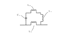
図3は、EBG構造4を構成しているEBG単位セル41に含まれる共振回路部分の等価回路を示している。図3において、各記号は以下のとおりである。
Lb:ブランチ部分のインダクタンス成分。
Cs:電源層パターンと容量結合素子との結合容量。
Lv:電源層パターンと容量結合素子とを接続するビア部分のインダクタンス成分。
Lw:容量結合素子からビアまでを接続する容量結合素子配線部分のインダクタンス成分。FIG. 3 shows an equivalent circuit of a resonance circuit portion included in the EBG unit cell 41 constituting the
Lb: an inductance component of the branch portion.
Cs: Coupling capacitance between the power supply layer pattern and the capacitive coupling element.
Lv: Inductance component of the via portion connecting the power supply layer pattern and the capacitive coupling element.
Lw: Inductance component of the capacitive coupling element wiring portion connecting the capacitive coupling element to the via.
電源層パターン42と容量結合素子43との層間の厚さは、特に限定されない。電源層パターン42と容量結合素子43との間に結合容量Csを有するようにするために、電源層パターン42と容量結合素子43との層間の厚さは25μm以下であってもよい。十分な結合容量Csを有するようにするために、層間の厚みは10〜20μm以下であってもよい。 The thickness between the power supply layer pattern 42 and the capacitive coupling element 43 is not particularly limited. In order to have a coupling capacitance Cs between the power supply layer pattern 42 and the capacitive coupling element 43, the thickness between the power supply layer pattern 42 and the capacitive coupling element 43 may be 25 μm or less. In order to have a sufficient coupling capacitance Cs, the thickness between the layers may be 10 to 20 μm or less.
EBG構造4は、この容量結合CsがインダクタンスLvとLwを介して接続され、電源層電極421の少なくとも一部を囲むように形成されたブランチ422で発生するインダクタンスLbを使い共振させる。容量結合素子43に、容量結合素子本体431の少なくとも一部を囲むように容量結合素子配線432の経路を長くし、インダクタンスLwを大きくする。これにより、見かけ上容量結合Csを大きくすることができるため、並列共振周波数を下げることができる。これは、EBG単位セル41を小さくできることを示しており、その結果、EBG構造4を小型化することが可能となる。EBG単位セル41の大きさは、略矩形状の場合、例えば縦横がそれぞれ3mm以下であり、1.5mm以下であってもよい。
In the
図4は、EBG単位セル41中の共振回路の共振周波数を求めるための電磁界シミュレーション結果を示すグラフである。この共振解析結果から、EBG構造4は、EBG単位セルが1.95mm×1.85mmにもかかわらず、2.4GHz付近の帯域に電磁ノイズ伝搬を抑制する阻止域を設定できることがわかる。
FIG. 4 is a graph showing the electromagnetic field simulation result for obtaining the resonance frequency of the resonance circuit in the EBG unit cell 41. From this resonance analysis result, it can be seen that the
次に、本開示の印刷配線板に設けられているEBG構造の他の実施形態を、図5(A)〜(C)に基づいて説明する。 Next, another embodiment of the EBG structure provided in the printed wiring board of the present disclosure will be described based on FIGS.
図5(A)は、図1に示す印刷配線板1に設けられたEBG構造4の一部分を示す。図5(A)に示すように、EBG構造4’は、複数のEBG単位セル41’で形成されている。図5(A)は、図1に示すEBG構造4のうち、ブランチ422に沿った方向に3つ並べて配置したEBG単位セル41’を抜き出して示している。
FIG. 5A shows a part of the
図5(A)に示すEBG単位セル41’と図2(A)に示すEBG単位セル41とは、電源層パターンに設けられた電源層配線423および容量結合素子に設けられた容量結合素子配線432’の長さが相違する。すなわち、図2(A)に示すEBG単位セル41では、図2(B)に示すように電源層パターン42に電源層配線は存在せず、図2(C)に示すように容量結合素子43の容量結合素子配線432は略矩形状の容量結合素子本体431の略一辺の長さを有している。一方、図5(A)に示すEBG単位セル41’では、電源層パターン42’の電源層配線423および容量結合素子43’の容量結合素子配線432’が、図5(B)および(C)に示すように、略矩形状の電源層電極421’および略矩形状の容量結合素子本体431’の周囲をそれぞれ、略一辺および略半周分囲んでいる。 The EBG unit cell 41 ′ shown in FIG. 5A and the EBG unit cell 41 shown in FIG. 2A include a power supply layer wiring 423 provided in the power supply layer pattern and a capacitive coupling element wiring provided in the capacitive coupling element. The length of 432 ′ is different. That is, in the EBG unit cell 41 shown in FIG. 2A, there is no power supply layer wiring in the power supply layer pattern 42 as shown in FIG. 2B, and the capacitive coupling element 43 as shown in FIG. The capacitive coupling element wiring 432 has a length of substantially one side of a substantially rectangular capacitive coupling element body 431. On the other hand, in the EBG unit cell 41 ′ shown in FIG. 5A, the power supply layer wiring 423 of the power supply layer pattern 42 ′ and the capacitive coupling element wiring 432 ′ of the capacitive coupling element 43 ′ are shown in FIGS. As shown in FIG. 3, the power supply layer electrode 421 ′ having a substantially rectangular shape and the capacitive coupling element body 431 ′ having a substantially rectangular shape are surrounded by a substantially one side and a substantially half circumference, respectively.
具体的には、図5(B)に示すように、電源層パターン42’は、電源層2の一部において、スリットを形成することによって、電源層電極421’、ブランチ422’および電源層配線423に区別されている。電源層電極421’は略矩形を有している。電源層配線423は、電源層電極421’の1つの角部421aから隣接する一方の角部421bまで、電源層電極421’の略一辺の長さを有している。ブランチ422’は、隣接する電源層配線423を介して、その先端部で電源層電極421’の1つの角部と接続されている。ブランチ422’と電源層電極421’の1つの角部との接続は、隣接する電源層配線423を介さないで、両者の一部で直接接続されるのでもよい。
Specifically, as shown in FIG. 5B, the power supply layer pattern 42 ′ is formed by forming slits in a part of the
図5(C)に示すように、容量結合素子本体431’は略矩形を有しており、電源層電極421’と略同じ大きさである。容量結合素子配線432’は、ブランチ422’の1つの角部421aと略同じ位置となるように、容量結合素子本体431’の周囲を半周以上囲むように形成されている。
As shown in FIG. 5C, the capacitive coupling element main body 431 'has a substantially rectangular shape and is approximately the same size as the power supply layer electrode 421'. The capacitive coupling element wiring 432 ′ is formed so as to surround the circumference of the capacitive coupling element main body 431 ′ by a half or more so as to be substantially at the same position as one corner 421 a of the
電源層電極421’と容量結合素子43’とは絶縁層5を介して容量結合されている。一方、電源層電極421’の一部とブランチ422’は隣接する電源層配線423を介するなどして接続される。同時に、容量結合素子43’から延在している容量結合素子配線432’の先端部でビアを介してブランチ422’と接続されている。ビアは、例えば銅などの導電性材料で形成されている。
The power supply layer electrode 421 ′ and the capacitive coupling element 43 ′ are capacitively coupled via the insulating
EBG構造4’を構成しているEBG単位セル41’に含まれる共振回路部分の等価回路は、図3に示すEBG構造4を構成しているEBG単位セル41に含まれる共振回路部分の等価回路と同じである。ただし、電源層パターン42’では電源層パターン42に存在しない電源層配線423が形成されている。さらに、容量結合素子43’では容量結合素子43に比べて容量結合素子配線432’の経路をより長くしている。そのため、両者のインダクタンス成分の総和であるインダクタンスLwは、EBG単位セル41’ではEBG単位セル41より大きくすることができる。インダクタンスLwを大きくすることで、見かけ上容量結合Csを大きくすることができるため、結果として並列共振周波数を下げることができる。これは、EBG単位セル41’をより小さくできることを示しており、その結果、EBG構造4’をより小型化することが可能となる。
The equivalent circuit of the resonance circuit part included in the EBG unit cell 41 ′ constituting the
図6は、EBG単位セル41’の共振回路の共振周波数を求めるための電磁界シミュレーション結果を示すグラフである。この共振解析結果から、EBG構造4’は、EBG単位セルが1.5mm角にもかかわらず、2.4GHz付近の帯域に電磁ノイズ伝搬を抑制する阻止域を設定できることがわかる。
FIG. 6 is a graph showing electromagnetic field simulation results for obtaining the resonance frequency of the resonance circuit of the EBG unit cell 41 '. From this resonance analysis result, it can be seen that the
本開示の印刷配線板は、上述の実施形態に限定されない。例えば、上述のEBG構造4およびEBG構造4’は、略矩形状の電源層電極および容量結合素子本体を有している。しかし、電源層電極および容量結合素子本体の形状は限定されず、例えば、円形、多角形(五角形や六角形)、凹みがあるような他の形状を有していてもよい。
The printed wiring board of this indication is not limited to the above-mentioned embodiment. For example, the above-described
さらに、本開示の印刷配線板において、EBG構造を構成しているEBG単位セルの数は、特に限定されない。通常、ブランチに沿った方向に2〜4個程度であればよい。 Furthermore, in the printed wiring board of the present disclosure, the number of EBG unit cells constituting the EBG structure is not particularly limited. Usually, it may be about 2 to 4 in the direction along the branch.
1 印刷配線板
2 電源層
3 グラウンド層
4 EBG構造
41、41’ EBG単位セル
42、42’ 電源層パターン
421、421’ 電源層電極
421a、421b 角部
422、422’ ブランチ
423 電源層配線
43、43’ 容量結合素子
431、431’ 容量結合素子本体
431a 角部
432、432’ 容量結合素子配線
44、44’ ビア
5 絶縁層DESCRIPTION OF
Claims (4)
電源層に形成される電源層パターンが、隣接するEBG単位セル間を接続する直流給電路であるブランチと、電源層電極とを含み、
容量結合素子本体を含む容量結合素子が、前記電源層電極と対向するように層間を設けて配置され、
前記電源層パターンが、前記電源層電極から延在して該電極周囲の少なくとも一部を囲むように形成された電源層配線をさらに含むか、前記容量結合素子が、前記容量結合素子本体から延在して該本体周囲の少なくとも一部を囲むように形成された容量結合素子配線をさらに含むか、あるいは前記電源層パターンが前記電源層配線をさらに含みかつ前記容量結合素子が前記容量結合素子配線をさらに含み、
前記電源層パターンと前記容量結合素子とが、前記電源層配線および前記容量結合素子配線の少なくとも一方に接続されたビアを介して接続されるEBG単位セルが周期的に配置されたEBG構造を有する印刷配線板。Including power and ground layers,
The power supply layer pattern formed in the power supply layer includes a branch that is a DC power supply path that connects adjacent EBG unit cells, and a power supply layer electrode,
A capacitive coupling element including a capacitive coupling element body is disposed with an interlayer so as to face the power supply layer electrode,
The power supply layer pattern further includes a power supply layer wiring extending from the power supply layer electrode and surrounding at least a part of the periphery of the electrode, or the capacitive coupling element extends from the capacitive coupling element body. And further includes a capacitive coupling element wiring formed so as to surround at least a part of the periphery of the main body, or the power supply layer pattern further includes the power supply layer wiring and the capacitive coupling element includes the capacitive coupling element wiring. Further including
The power supply layer pattern and the capacitive coupling element have an EBG structure in which EBG unit cells connected via at least one of the power supply layer wiring and the capacitive coupling element wiring are periodically arranged. Printed wiring board.
前記ブランチが、スリットを形成することによって区別されている電源層電極の1つの角部から隣接する一方の角部近傍まで延在し、
前記容量結合素子配線が、容量結合素子本体の角部からブランチが延在している方向に延在し、
ブランチと容量結合素子配線とが、それぞれの先端部でビアを介して接続されている請求項1に記載の印刷配線板。The power supply layer electrode and the capacitive coupling element body are substantially rectangular and have substantially the same size,
The branch extends from one corner of the power supply layer electrode that is distinguished by forming a slit to the vicinity of one adjacent corner;
The capacitive coupling element wiring extends in a direction in which a branch extends from a corner of the capacitive coupling element body;
The printed wiring board according to claim 1, wherein the branch and the capacitive coupling element wiring are connected to each other at a leading end portion thereof via a via.
電源層配線と容量結合素子配線とが、それぞれの先端部でビアを介して接続されている請求項1に記載の印刷配線板。The power supply layer electrode and the capacitive coupling element main body are substantially rectangular and have substantially the same size, and the power supply layer wiring has a length of at least substantially one side around the power supply layer electrode. The wiring sees at least half the circumference of the capacitive coupling element body,
2. The printed wiring board according to claim 1, wherein the power supply layer wiring and the capacitive coupling element wiring are connected to each other at a leading end portion via a via.
Applications Claiming Priority (3)
| Application Number | Priority Date | Filing Date | Title |
|---|---|---|---|
| JP2016147672 | 2016-07-27 | ||
| JP2016147672 | 2016-07-27 | ||
| PCT/JP2017/026326 WO2018021148A1 (en) | 2016-07-27 | 2017-07-20 | Printed wiring board |
Publications (2)
| Publication Number | Publication Date |
|---|---|
| JPWO2018021148A1 JPWO2018021148A1 (en) | 2019-07-18 |
| JP6611065B2 true JP6611065B2 (en) | 2019-11-27 |
Family
ID=61016056
Family Applications (1)
| Application Number | Title | Priority Date | Filing Date |
|---|---|---|---|
| JP2018529826A Active JP6611065B2 (en) | 2016-07-27 | 2017-07-20 | Printed wiring board |
Country Status (6)
| Country | Link |
|---|---|
| US (1) | US10791622B2 (en) |
| JP (1) | JP6611065B2 (en) |
| KR (1) | KR102176897B1 (en) |
| CN (1) | CN109479378B (en) |
| TW (1) | TWI659676B (en) |
| WO (1) | WO2018021148A1 (en) |
Families Citing this family (2)
| Publication number | Priority date | Publication date | Assignee | Title |
|---|---|---|---|---|
| JP6804261B2 (en) * | 2016-10-27 | 2020-12-23 | 京セラ株式会社 | Printed circuit board for relay |
| CN111800937B (en) * | 2020-06-19 | 2021-12-21 | 苏州浪潮智能科技有限公司 | Electromagnetic band gap structure and PCB |
Family Cites Families (52)
| Publication number | Priority date | Publication date | Assignee | Title |
|---|---|---|---|---|
| US7215007B2 (en) * | 2003-06-09 | 2007-05-08 | Wemtec, Inc. | Circuit and method for suppression of electromagnetic coupling and switching noise in multilayer printed circuit boards |
| US20050224912A1 (en) * | 2004-03-17 | 2005-10-13 | Rogers Shawn D | Circuit and method for enhanced low frequency switching noise suppression in multilayer printed circuit boards using a chip capacitor lattice |
| US7626216B2 (en) * | 2005-10-21 | 2009-12-01 | Mckinzie Iii William E | Systems and methods for electromagnetic noise suppression using hybrid electromagnetic bandgap structures |
| TW200818451A (en) * | 2006-06-02 | 2008-04-16 | Renesas Tech Corp | Semiconductor device |
| TW200808136A (en) | 2006-07-26 | 2008-02-01 | Inventec Corp | A layout design for a multilayer printed circuit board |
| JP4755966B2 (en) * | 2006-11-22 | 2011-08-24 | Necトーキン株式会社 | EBG structure and noise filter |
| US20080158840A1 (en) * | 2006-12-27 | 2008-07-03 | Inventec Corporation | DC power plane structure |
| US7839654B2 (en) * | 2007-02-28 | 2010-11-23 | International Business Machines Corporation | Method for ultimate noise isolation in high-speed digital systems on packages and printed circuit boards (PCBS) |
| US7855696B2 (en) * | 2007-03-16 | 2010-12-21 | Rayspan Corporation | Metamaterial antenna arrays with radiation pattern shaping and beam switching |
| KR100838246B1 (en) * | 2007-06-22 | 2008-06-17 | 삼성전기주식회사 | Printed circuit board having electromagnetic bandgap structure |
| KR100838244B1 (en) * | 2007-06-22 | 2008-06-17 | 삼성전기주식회사 | Electromagnetic bandgap structure and printed circuit board |
| US8158889B2 (en) * | 2007-06-22 | 2012-04-17 | Samsung Electro-Mechanics Co., Ltd. | Electromagnetic bandgap structure and printed circuit board |
| KR100871346B1 (en) | 2007-06-22 | 2008-12-01 | 삼성전기주식회사 | Electromagnetic bandgap structure and printed circuit board |
| US8169790B2 (en) * | 2007-08-07 | 2012-05-01 | Samsung Electro-Mechanics Co., Ltd. | Electromagnetic bandgap structure and printed circuit board |
| EP2227859B1 (en) * | 2007-11-16 | 2017-11-01 | Gula Consulting Limited Liability Company | Filter design methods and filters based on metamaterial structures |
| TWI375499B (en) * | 2007-11-27 | 2012-10-21 | Asustek Comp Inc | Improvement method for ebg structures and multi-layer board applying the same |
| DE102008045055A1 (en) * | 2007-12-07 | 2009-06-10 | Samsung Electro-Mechanics Co., Ltd., Suwon | Electromagnetic bandgap structure and circuit board |
| TWI397931B (en) * | 2008-02-29 | 2013-06-01 | Ind Tech Res Inst | Capacitor devices |
| JP5380919B2 (en) * | 2008-06-24 | 2014-01-08 | 日本電気株式会社 | Waveguide structure and printed wiring board |
| KR100956689B1 (en) * | 2008-06-27 | 2010-05-10 | 삼성전기주식회사 | Electromagnetic bandgap structure and printed circuit board |
| JP5522042B2 (en) * | 2008-08-01 | 2014-06-18 | 日本電気株式会社 | Structure, printed circuit board, antenna, transmission line waveguide converter, array antenna, electronic device |
| US20100060527A1 (en) * | 2008-09-10 | 2010-03-11 | International Business Machines Corporation | Electromagnetic band gap tuning using undulating branches |
| WO2010029770A1 (en) * | 2008-09-11 | 2010-03-18 | 日本電気株式会社 | Structure, antenna, communication device, and electronic component |
| US8288660B2 (en) * | 2008-10-03 | 2012-10-16 | International Business Machines Corporation | Preserving stopband characteristics of electromagnetic bandgap structures in circuit boards |
| KR100999550B1 (en) * | 2008-10-08 | 2010-12-08 | 삼성전기주식회사 | Electro-magnetic bandgap structure |
| DE102008051531B4 (en) * | 2008-10-14 | 2013-04-18 | Fraunhofer-Gesellschaft zur Förderung der angewandten Forschung e.V. | Electrical system with a device for suppressing the propagation of electromagnetic interference |
| FI124128B (en) * | 2008-10-28 | 2014-03-31 | Tellabs Oy | filter Design |
| KR101018807B1 (en) * | 2008-12-02 | 2011-03-03 | 삼성전기주식회사 | Electromagnetic bandgap structure and circuit board |
| KR101018796B1 (en) * | 2008-12-02 | 2011-03-03 | 삼성전기주식회사 | Electromagnetic bandgap structure and circuit board |
| JP5326649B2 (en) * | 2009-02-24 | 2013-10-30 | 日本電気株式会社 | Antenna, array antenna, printed circuit board, and electronic device using the same |
| KR101055457B1 (en) * | 2009-04-07 | 2011-08-08 | 포항공과대학교 산학협력단 | Electromagnetic bandgap structure and printed circuit board including the same |
| KR101055483B1 (en) * | 2009-04-07 | 2011-08-08 | 포항공과대학교 산학협력단 | Electromagnetic bandgap structure and printed circuit board including the same |
| CN101667567B (en) | 2009-07-06 | 2011-08-17 | 深圳先进技术研究院 | Electromagnetism interference isolation device |
| KR101007288B1 (en) * | 2009-07-29 | 2011-01-13 | 삼성전기주식회사 | Printed circuit board and electro application |
| KR101072591B1 (en) * | 2009-08-10 | 2011-10-11 | 삼성전기주식회사 | Electromagnetic interference noise reduction board using electromagnetic bandgap structure |
| KR101021548B1 (en) * | 2009-09-18 | 2011-03-16 | 삼성전기주식회사 | Printed circuit board having electromagnetic bandgap structure |
| KR101023541B1 (en) * | 2009-09-22 | 2011-03-21 | 삼성전기주식회사 | Electromagnetic interference noise reduction board using electromagnetic bandgap structure |
| KR101021551B1 (en) * | 2009-09-22 | 2011-03-16 | 삼성전기주식회사 | Printed circuit board having electromagnetic bandgap structure |
| KR101092590B1 (en) * | 2009-09-23 | 2011-12-13 | 삼성전기주식회사 | printed circuit board having electromagnetic bandgap structure |
| KR101308970B1 (en) * | 2009-12-21 | 2013-09-17 | 한국전자통신연구원 | Multi layer PCB for suppressing the unwanted electromagnetic fields and noise |
| KR101044789B1 (en) * | 2010-01-04 | 2011-06-29 | 삼성전기주식회사 | Electromagnetic bandgap structure and circuit board |
| JP2013058585A (en) | 2011-09-08 | 2013-03-28 | Oki Printed Circuits Co Ltd | Multilayer printed wiring board |
| JP2013183082A (en) | 2012-03-02 | 2013-09-12 | Oki Printed Circuits Co Ltd | Multilayer printed board |
| JP2013232613A (en) * | 2012-04-05 | 2013-11-14 | Sony Corp | Wiring board and electronic apparatus |
| JP5694251B2 (en) | 2012-07-27 | 2015-04-01 | 株式会社東芝 | EBG structure and circuit board |
| KR20140102462A (en) * | 2013-02-14 | 2014-08-22 | 한국전자통신연구원 | Electromagnetic bandgap structure and method for manufacturing the electromagnetic bandgap structure |
| CN104080263A (en) * | 2013-03-29 | 2014-10-01 | 鸿富锦精密工业(深圳)有限公司 | Stack-based electromagnetic energy gap structure |
| JP5660168B2 (en) | 2013-07-25 | 2015-01-28 | 日本電気株式会社 | Waveguide structure, printed wiring board, and electronic device using the same |
| JP6168943B2 (en) * | 2013-09-20 | 2017-07-26 | 株式会社東芝 | EBG structure, semiconductor device and circuit board |
| JP5929969B2 (en) * | 2014-06-12 | 2016-06-08 | ヤマハ株式会社 | Printed circuit board and noise reduction method in printed circuit board |
| JP6894602B2 (en) * | 2014-11-28 | 2021-06-30 | 国立大学法人 岡山大学 | Printed wiring board and its manufacturing method |
| US10178758B2 (en) * | 2014-11-28 | 2019-01-08 | National University Corporation Okayama University | Printed wiring board and method of producing the same |
-
2017
- 2017-07-20 JP JP2018529826A patent/JP6611065B2/en active Active
- 2017-07-20 US US16/320,392 patent/US10791622B2/en active Active
- 2017-07-20 KR KR1020197002262A patent/KR102176897B1/en active IP Right Grant
- 2017-07-20 WO PCT/JP2017/026326 patent/WO2018021148A1/en active Application Filing
- 2017-07-20 CN CN201780046116.0A patent/CN109479378B/en active Active
- 2017-07-26 TW TW106125105A patent/TWI659676B/en active
Also Published As
| Publication number | Publication date |
|---|---|
| KR20190021400A (en) | 2019-03-05 |
| TW201811128A (en) | 2018-03-16 |
| CN109479378B (en) | 2021-04-23 |
| KR102176897B1 (en) | 2020-11-10 |
| CN109479378A (en) | 2019-03-15 |
| JPWO2018021148A1 (en) | 2019-07-18 |
| US10791622B2 (en) | 2020-09-29 |
| US20190246494A1 (en) | 2019-08-08 |
| WO2018021148A1 (en) | 2018-02-01 |
| TWI659676B (en) | 2019-05-11 |
Similar Documents
| Publication | Publication Date | Title |
|---|---|---|
| JP6168943B2 (en) | EBG structure, semiconductor device and circuit board | |
| WO2006067939A1 (en) | Multilayer capacitor and mounting structure of same | |
| US7498815B2 (en) | Array antenna for magnetic resonance applications | |
| JP6611065B2 (en) | Printed wiring board | |
| JP2016006816A (en) | Transformer and multilayer substrate | |
| JP6611066B2 (en) | Printed wiring board | |
| US20150130580A1 (en) | Common mode filter and manufacturing method thereof | |
| JP2011061126A (en) | Circuit board | |
| JP2020043172A (en) | Electronic equipment | |
| US8125794B2 (en) | Multilayer printed wiring board and electronic device using the same | |
| JP2013012528A (en) | Printed board | |
| JP6804261B2 (en) | Printed circuit board for relay | |
| JP6884616B2 (en) | Printed wiring board | |
| JP6744201B2 (en) | Printed wiring board | |
| US8802995B2 (en) | Electronic component including multilayer substrate | |
| TWI671997B (en) | Oscillator structure | |
| JP2018056312A (en) | Printed-circuit board | |
| US9496845B2 (en) | Common mode filter and method for manufacturing the same | |
| JP2020088255A (en) | Wiring board | |
| JP2006303020A (en) | Capacitor built-in printed wiring board | |
| US20150114688A1 (en) | Printed circuit board | |
| JP2011071792A (en) | Laminated dielectric filter |
Legal Events
| Date | Code | Title | Description |
|---|---|---|---|
| A621 | Written request for application examination |
Free format text: JAPANESE INTERMEDIATE CODE: A621 Effective date: 20190124 |
|
| A521 | Request for written amendment filed |
Free format text: JAPANESE INTERMEDIATE CODE: A523 Effective date: 20190208 |
|
| AA64 | Notification of invalidation of claim of internal priority (with term) |
Free format text: JAPANESE INTERMEDIATE CODE: A241764 Effective date: 20190402 |
|
| A521 | Request for written amendment filed |
Free format text: JAPANESE INTERMEDIATE CODE: A523 Effective date: 20190424 |
|
| TRDD | Decision of grant or rejection written | ||
| A01 | Written decision to grant a patent or to grant a registration (utility model) |
Free format text: JAPANESE INTERMEDIATE CODE: A01 Effective date: 20191001 |
|
| A61 | First payment of annual fees (during grant procedure) |
Free format text: JAPANESE INTERMEDIATE CODE: A61 Effective date: 20191018 |
|
| R150 | Certificate of patent or registration of utility model |
Ref document number: 6611065 Country of ref document: JP Free format text: JAPANESE INTERMEDIATE CODE: R150 |
|
| R250 | Receipt of annual fees |
Free format text: JAPANESE INTERMEDIATE CODE: R250 |
|
| R250 | Receipt of annual fees |
Free format text: JAPANESE INTERMEDIATE CODE: R250 |