JP6592104B2 - Flexible display device - Google Patents
Flexible display device Download PDFInfo
- Publication number
- JP6592104B2 JP6592104B2 JP2017553816A JP2017553816A JP6592104B2 JP 6592104 B2 JP6592104 B2 JP 6592104B2 JP 2017553816 A JP2017553816 A JP 2017553816A JP 2017553816 A JP2017553816 A JP 2017553816A JP 6592104 B2 JP6592104 B2 JP 6592104B2
- Authority
- JP
- Japan
- Prior art keywords
- circuit
- pixel circuit
- display
- driving
- organic
- Prior art date
- Legal status (The legal status is an assumption and is not a legal conclusion. Google has not performed a legal analysis and makes no representation as to the accuracy of the status listed.)
- Active
Links
- 238000005259 measurement Methods 0.000 claims description 132
- 238000005452 bending Methods 0.000 claims description 105
- 238000001514 detection method Methods 0.000 claims description 84
- 238000012937 correction Methods 0.000 claims description 71
- 230000008859 change Effects 0.000 claims description 22
- 238000005401 electroluminescence Methods 0.000 description 160
- 238000010586 diagram Methods 0.000 description 24
- 230000006870 function Effects 0.000 description 14
- 230000032683 aging Effects 0.000 description 12
- 239000003990 capacitor Substances 0.000 description 10
- 238000000034 method Methods 0.000 description 6
- 238000013500 data storage Methods 0.000 description 5
- 230000007274 generation of a signal involved in cell-cell signaling Effects 0.000 description 5
- 230000000295 complement effect Effects 0.000 description 4
- 238000012545 processing Methods 0.000 description 4
- 230000007547 defect Effects 0.000 description 2
- 230000008569 process Effects 0.000 description 2
- 239000000758 substrate Substances 0.000 description 2
- 230000009471 action Effects 0.000 description 1
- 229910021417 amorphous silicon Inorganic materials 0.000 description 1
- 230000015572 biosynthetic process Effects 0.000 description 1
- 238000006243 chemical reaction Methods 0.000 description 1
- 239000000470 constituent Substances 0.000 description 1
- 229910021419 crystalline silicon Inorganic materials 0.000 description 1
- 230000007423 decrease Effects 0.000 description 1
- 238000005516 engineering process Methods 0.000 description 1
- 239000000463 material Substances 0.000 description 1
- 230000004048 modification Effects 0.000 description 1
- 238000012986 modification Methods 0.000 description 1
- 230000004044 response Effects 0.000 description 1
- 239000004065 semiconductor Substances 0.000 description 1
- 239000010409 thin film Substances 0.000 description 1
- 230000003936 working memory Effects 0.000 description 1
Images


Classifications
-
- G—PHYSICS
- G09—EDUCATION; CRYPTOGRAPHY; DISPLAY; ADVERTISING; SEALS
- G09G—ARRANGEMENTS OR CIRCUITS FOR CONTROL OF INDICATING DEVICES USING STATIC MEANS TO PRESENT VARIABLE INFORMATION
- G09G3/00—Control arrangements or circuits, of interest only in connection with visual indicators other than cathode-ray tubes
- G09G3/20—Control arrangements or circuits, of interest only in connection with visual indicators other than cathode-ray tubes for presentation of an assembly of a number of characters, e.g. a page, by composing the assembly by combination of individual elements arranged in a matrix no fixed position being assigned to or needed to be assigned to the individual characters or partial characters
- G09G3/22—Control arrangements or circuits, of interest only in connection with visual indicators other than cathode-ray tubes for presentation of an assembly of a number of characters, e.g. a page, by composing the assembly by combination of individual elements arranged in a matrix no fixed position being assigned to or needed to be assigned to the individual characters or partial characters using controlled light sources
- G09G3/30—Control arrangements or circuits, of interest only in connection with visual indicators other than cathode-ray tubes for presentation of an assembly of a number of characters, e.g. a page, by composing the assembly by combination of individual elements arranged in a matrix no fixed position being assigned to or needed to be assigned to the individual characters or partial characters using controlled light sources using electroluminescent panels
- G09G3/32—Control arrangements or circuits, of interest only in connection with visual indicators other than cathode-ray tubes for presentation of an assembly of a number of characters, e.g. a page, by composing the assembly by combination of individual elements arranged in a matrix no fixed position being assigned to or needed to be assigned to the individual characters or partial characters using controlled light sources using electroluminescent panels semiconductive, e.g. using light-emitting diodes [LED]
- G09G3/3208—Control arrangements or circuits, of interest only in connection with visual indicators other than cathode-ray tubes for presentation of an assembly of a number of characters, e.g. a page, by composing the assembly by combination of individual elements arranged in a matrix no fixed position being assigned to or needed to be assigned to the individual characters or partial characters using controlled light sources using electroluminescent panels semiconductive, e.g. using light-emitting diodes [LED] organic, e.g. using organic light-emitting diodes [OLED]
- G09G3/3225—Control arrangements or circuits, of interest only in connection with visual indicators other than cathode-ray tubes for presentation of an assembly of a number of characters, e.g. a page, by composing the assembly by combination of individual elements arranged in a matrix no fixed position being assigned to or needed to be assigned to the individual characters or partial characters using controlled light sources using electroluminescent panels semiconductive, e.g. using light-emitting diodes [LED] organic, e.g. using organic light-emitting diodes [OLED] using an active matrix
- G09G3/3233—Control arrangements or circuits, of interest only in connection with visual indicators other than cathode-ray tubes for presentation of an assembly of a number of characters, e.g. a page, by composing the assembly by combination of individual elements arranged in a matrix no fixed position being assigned to or needed to be assigned to the individual characters or partial characters using controlled light sources using electroluminescent panels semiconductive, e.g. using light-emitting diodes [LED] organic, e.g. using organic light-emitting diodes [OLED] using an active matrix with pixel circuitry controlling the current through the light-emitting element
-
- G—PHYSICS
- G01—MEASURING; TESTING
- G01B—MEASURING LENGTH, THICKNESS OR SIMILAR LINEAR DIMENSIONS; MEASURING ANGLES; MEASURING AREAS; MEASURING IRREGULARITIES OF SURFACES OR CONTOURS
- G01B7/00—Measuring arrangements characterised by the use of electric or magnetic techniques
- G01B7/16—Measuring arrangements characterised by the use of electric or magnetic techniques for measuring the deformation in a solid, e.g. by resistance strain gauge
-
- G—PHYSICS
- G09—EDUCATION; CRYPTOGRAPHY; DISPLAY; ADVERTISING; SEALS
- G09G—ARRANGEMENTS OR CIRCUITS FOR CONTROL OF INDICATING DEVICES USING STATIC MEANS TO PRESENT VARIABLE INFORMATION
- G09G3/00—Control arrangements or circuits, of interest only in connection with visual indicators other than cathode-ray tubes
- G09G3/20—Control arrangements or circuits, of interest only in connection with visual indicators other than cathode-ray tubes for presentation of an assembly of a number of characters, e.g. a page, by composing the assembly by combination of individual elements arranged in a matrix no fixed position being assigned to or needed to be assigned to the individual characters or partial characters
- G09G3/22—Control arrangements or circuits, of interest only in connection with visual indicators other than cathode-ray tubes for presentation of an assembly of a number of characters, e.g. a page, by composing the assembly by combination of individual elements arranged in a matrix no fixed position being assigned to or needed to be assigned to the individual characters or partial characters using controlled light sources
- G09G3/30—Control arrangements or circuits, of interest only in connection with visual indicators other than cathode-ray tubes for presentation of an assembly of a number of characters, e.g. a page, by composing the assembly by combination of individual elements arranged in a matrix no fixed position being assigned to or needed to be assigned to the individual characters or partial characters using controlled light sources using electroluminescent panels
- G09G3/32—Control arrangements or circuits, of interest only in connection with visual indicators other than cathode-ray tubes for presentation of an assembly of a number of characters, e.g. a page, by composing the assembly by combination of individual elements arranged in a matrix no fixed position being assigned to or needed to be assigned to the individual characters or partial characters using controlled light sources using electroluminescent panels semiconductive, e.g. using light-emitting diodes [LED]
- G09G3/3208—Control arrangements or circuits, of interest only in connection with visual indicators other than cathode-ray tubes for presentation of an assembly of a number of characters, e.g. a page, by composing the assembly by combination of individual elements arranged in a matrix no fixed position being assigned to or needed to be assigned to the individual characters or partial characters using controlled light sources using electroluminescent panels semiconductive, e.g. using light-emitting diodes [LED] organic, e.g. using organic light-emitting diodes [OLED]
- G09G3/3266—Details of drivers for scan electrodes
-
- G—PHYSICS
- G09—EDUCATION; CRYPTOGRAPHY; DISPLAY; ADVERTISING; SEALS
- G09G—ARRANGEMENTS OR CIRCUITS FOR CONTROL OF INDICATING DEVICES USING STATIC MEANS TO PRESENT VARIABLE INFORMATION
- G09G3/00—Control arrangements or circuits, of interest only in connection with visual indicators other than cathode-ray tubes
- G09G3/20—Control arrangements or circuits, of interest only in connection with visual indicators other than cathode-ray tubes for presentation of an assembly of a number of characters, e.g. a page, by composing the assembly by combination of individual elements arranged in a matrix no fixed position being assigned to or needed to be assigned to the individual characters or partial characters
- G09G3/22—Control arrangements or circuits, of interest only in connection with visual indicators other than cathode-ray tubes for presentation of an assembly of a number of characters, e.g. a page, by composing the assembly by combination of individual elements arranged in a matrix no fixed position being assigned to or needed to be assigned to the individual characters or partial characters using controlled light sources
- G09G3/30—Control arrangements or circuits, of interest only in connection with visual indicators other than cathode-ray tubes for presentation of an assembly of a number of characters, e.g. a page, by composing the assembly by combination of individual elements arranged in a matrix no fixed position being assigned to or needed to be assigned to the individual characters or partial characters using controlled light sources using electroluminescent panels
- G09G3/32—Control arrangements or circuits, of interest only in connection with visual indicators other than cathode-ray tubes for presentation of an assembly of a number of characters, e.g. a page, by composing the assembly by combination of individual elements arranged in a matrix no fixed position being assigned to or needed to be assigned to the individual characters or partial characters using controlled light sources using electroluminescent panels semiconductive, e.g. using light-emitting diodes [LED]
- G09G3/3208—Control arrangements or circuits, of interest only in connection with visual indicators other than cathode-ray tubes for presentation of an assembly of a number of characters, e.g. a page, by composing the assembly by combination of individual elements arranged in a matrix no fixed position being assigned to or needed to be assigned to the individual characters or partial characters using controlled light sources using electroluminescent panels semiconductive, e.g. using light-emitting diodes [LED] organic, e.g. using organic light-emitting diodes [OLED]
- G09G3/3275—Details of drivers for data electrodes
-
- G—PHYSICS
- G09—EDUCATION; CRYPTOGRAPHY; DISPLAY; ADVERTISING; SEALS
- G09G—ARRANGEMENTS OR CIRCUITS FOR CONTROL OF INDICATING DEVICES USING STATIC MEANS TO PRESENT VARIABLE INFORMATION
- G09G2320/00—Control of display operating conditions
- G09G2320/02—Improving the quality of display appearance
- G09G2320/0233—Improving the luminance or brightness uniformity across the screen
-
- G—PHYSICS
- G09—EDUCATION; CRYPTOGRAPHY; DISPLAY; ADVERTISING; SEALS
- G09G—ARRANGEMENTS OR CIRCUITS FOR CONTROL OF INDICATING DEVICES USING STATIC MEANS TO PRESENT VARIABLE INFORMATION
- G09G2320/00—Control of display operating conditions
- G09G2320/02—Improving the quality of display appearance
- G09G2320/0242—Compensation of deficiencies in the appearance of colours
-
- G—PHYSICS
- G09—EDUCATION; CRYPTOGRAPHY; DISPLAY; ADVERTISING; SEALS
- G09G—ARRANGEMENTS OR CIRCUITS FOR CONTROL OF INDICATING DEVICES USING STATIC MEANS TO PRESENT VARIABLE INFORMATION
- G09G2320/00—Control of display operating conditions
- G09G2320/02—Improving the quality of display appearance
- G09G2320/0285—Improving the quality of display appearance using tables for spatial correction of display data
-
- G—PHYSICS
- G09—EDUCATION; CRYPTOGRAPHY; DISPLAY; ADVERTISING; SEALS
- G09G—ARRANGEMENTS OR CIRCUITS FOR CONTROL OF INDICATING DEVICES USING STATIC MEANS TO PRESENT VARIABLE INFORMATION
- G09G2320/00—Control of display operating conditions
- G09G2320/02—Improving the quality of display appearance
- G09G2320/029—Improving the quality of display appearance by monitoring one or more pixels in the display panel, e.g. by monitoring a fixed reference pixel
- G09G2320/0295—Improving the quality of display appearance by monitoring one or more pixels in the display panel, e.g. by monitoring a fixed reference pixel by monitoring each display pixel
-
- G—PHYSICS
- G09—EDUCATION; CRYPTOGRAPHY; DISPLAY; ADVERTISING; SEALS
- G09G—ARRANGEMENTS OR CIRCUITS FOR CONTROL OF INDICATING DEVICES USING STATIC MEANS TO PRESENT VARIABLE INFORMATION
- G09G2320/00—Control of display operating conditions
- G09G2320/04—Maintaining the quality of display appearance
- G09G2320/043—Preventing or counteracting the effects of ageing
-
- G—PHYSICS
- G09—EDUCATION; CRYPTOGRAPHY; DISPLAY; ADVERTISING; SEALS
- G09G—ARRANGEMENTS OR CIRCUITS FOR CONTROL OF INDICATING DEVICES USING STATIC MEANS TO PRESENT VARIABLE INFORMATION
- G09G2320/00—Control of display operating conditions
- G09G2320/06—Adjustment of display parameters
- G09G2320/0693—Calibration of display systems
-
- G—PHYSICS
- G09—EDUCATION; CRYPTOGRAPHY; DISPLAY; ADVERTISING; SEALS
- G09G—ARRANGEMENTS OR CIRCUITS FOR CONTROL OF INDICATING DEVICES USING STATIC MEANS TO PRESENT VARIABLE INFORMATION
- G09G2380/00—Specific applications
- G09G2380/02—Flexible displays
Landscapes
- Engineering & Computer Science (AREA)
- Physics & Mathematics (AREA)
- General Physics & Mathematics (AREA)
- Computer Hardware Design (AREA)
- Theoretical Computer Science (AREA)
- Electroluminescent Light Sources (AREA)
- Control Of El Displays (AREA)
- Control Of Indicators Other Than Cathode Ray Tubes (AREA)
Description
本発明は、表示装置に関し、特に、屈曲可能な画面を有するフレキシブル表示装置に関する。 The present invention relates to a display device, and more particularly to a flexible display device having a bendable screen.
近年、薄型、低消費電力、高速応答可能な表示装置として、有機EL(Electro Luminescence)表示装置が注目されている。有機EL表示装置は、プラスチック基板などを用いて、画面を任意の位置で屈曲可能に構成することができる(図14を参照)。以下、屈曲可能な画面を有する表示装置を「フレキシブル表示装置」という。 In recent years, an organic EL (Electro Luminescence) display device has attracted attention as a display device that is thin, low power consumption, and capable of high-speed response. In the organic EL display device, a screen can be bent at an arbitrary position using a plastic substrate or the like (see FIG. 14). Hereinafter, a display device having a bendable screen is referred to as a “flexible display device”.
フレキシブル表示装置については、以下の技術が知られている。特許文献1には、図15に示す相補型回路を含むセンサーデバイスが記載されている。図15に示す相補型回路では、4個のトランジスタTr1〜Tr4のうち少なくとも1つが有機TFT(Thin Film Transistor)である。有機TFTの電気的特性は物理的変化に応じて変化するので、有機TFTはセンサー素子として機能する。
The following technologies are known for flexible display devices.
特許文献2には、図16に示す画素回路を含む表示装置が記載されている。図16に示す画素回路は、駆動素子として、相補型のトランジスタTp、Tnを含んでいる。画面が屈曲したときに、トランジスタTp、Tnの特性は逆方向に変化する。一方のトランジスタを流れる電流は増加し、他方のトランジスタを流れる電流は減少するので、画素回路全体として電流の変動を抑制することができる。
フレキシブル表示装置では、画面が屈曲したときに、画素回路内の駆動素子の特性(閾値電圧やI−V特性など)が変化し、駆動素子を通過して発光素子を流れる電流の量が変化する。このため、フレキシブル表示装置には、画面屈曲時に輝度や色が変化するという問題がある。 In the flexible display device, when the screen is bent, the characteristics (threshold voltage, IV characteristic, etc.) of the drive element in the pixel circuit change, and the amount of current flowing through the light emitting element through the drive element changes. . For this reason, the flexible display device has a problem that luminance and color change when the screen is bent.
従来のフレキシブル表示装置は、この問題を好適に解決することができない。例えば、特許文献1に記載された、センサー素子として有機TFTを用いる方法には、画面屈曲に起因するTFTの特性変化と、他の要因によるTFTの特性変化とを区別できないという問題がある。また、この方法には、検出される電流量が大きいという問題もある。
The conventional flexible display device cannot suitably solve this problem. For example, the method of using an organic TFT as a sensor element described in
それ故に、本発明は、画面の屈曲状態を検出し、画面屈曲時の輝度や色の変化を防止できる表示装置を提供することを目的とする。 Therefore, an object of the present invention is to provide a display device that can detect a bent state of a screen and prevent changes in luminance and color when the screen is bent.
本発明の第1の局面は、フレキシブル表示装置であって、
複数の走査線と、複数のデータ線と、それぞれが発光素子および駆動素子を有する複数の画素回路とを含む屈曲可能な表示パネルと、
前記走査線を駆動することにより、前記画素回路を選択する走査線駆動回路と、
前記データ線を駆動することにより、前記走査線駆動回路によって選択された画素回路について、前記駆動素子の制御端子に電圧を書き込む動作、および、前記駆動素子を流れる電流を測定する動作を行うデータ線駆動回路と、
屈曲検出部とを備え、
前記画素回路は、表示用画素回路と測定用画素回路とに分類され、
前記屈曲検出部は、前記測定用画素回路内の駆動素子を流れる電流を測定した結果に基づき、前記表示パネルの屈曲状態を検出し、
前記測定用画素回路の配置間隔は、前記表示用画素回路の配置間隔よりも狭いことを特徴とする。
A first aspect of the present invention is a flexible display device,
A bendable display panel including a plurality of scanning lines, a plurality of data lines, and a plurality of pixel circuits each having a light emitting element and a driving element;
A scanning line driving circuit for selecting the pixel circuit by driving the scanning line;
A data line that performs an operation of writing a voltage to a control terminal of the drive element and an operation of measuring a current flowing through the drive element for the pixel circuit selected by the scanning line drive circuit by driving the data line A drive circuit;
A bending detection unit,
The pixel circuit is classified into a display pixel circuit and a measurement pixel circuit,
The bending detection unit detects a bending state of the display panel based on a result of measuring a current flowing through a driving element in the measurement pixel circuit,
The arrangement interval of the measurement pixel circuits is narrower than the arrangement interval of the display pixel circuits.
本発明の第2の局面は、フレキシブル表示装置であって、
複数の走査線と、複数のデータ線と、それぞれが駆動素子を有する複数の画素回路とを含む屈曲可能な表示パネルと、
前記走査線を駆動することにより、前記画素回路を選択する走査線駆動回路と、
前記データ線を駆動することにより、前記走査線駆動回路によって選択された画素回路について、前記駆動素子の制御端子に電圧を書き込む動作、および、前記駆動素子を流れる電流を測定する動作を行うデータ線駆動回路と、
屈曲検出部とを備え、
前記画素回路は、複数の表示用画素回路と複数の測定用画素回路とに分類され、
前記屈曲検出部は、前記測定用画素回路内の駆動素子を流れる電流を測定した結果に基づき、前記表示パネルの屈曲状態を検出し、
前記表示パネルは、複数の前記表示用画素回路が形成された層と、複数の前記測定用画素回路が形成された層とを含む多層構造を有し、
複数の前記測定用画素回路は、それぞれ、前記複数の走査線のうち対応する走査線に接続され、
少なくとも一つの前記表示用画素回路に接続された走査線と、少なくとも一つの前記測定用画素回路に接続された対応する走査線とは、電気的に接続されていることを特徴とする。
A second aspect of the present invention is a flexible display device,
A plurality of scanning lines, a plurality of data lines, a bendable display panel including a plurality of pixel circuits, each with a driving dynamic element,
A scanning line driving circuit for selecting the pixel circuit by driving the scanning line;
A data line that performs an operation of writing a voltage to a control terminal of the drive element and an operation of measuring a current flowing through the drive element for the pixel circuit selected by the scanning line drive circuit by driving the data line A drive circuit;
A bending detection unit,
The pixel circuit is classified into a plurality of display pixel circuits and a plurality of measurement pixel circuits.
The bending detection unit detects a bending state of the display panel based on a result of measuring a current flowing through a driving element in the measurement pixel circuit,
The display panel, have a multilayered structure including a layer in which a plurality of the display pixel circuits are formed, and a plurality of layers in which the measuring pixel circuits are formed,
Each of the plurality of measurement pixel circuits is connected to a corresponding scanning line among the plurality of scanning lines,
A scan line connected to at least one of the display pixel circuit and the scan line corresponding connected to at least one of the measuring pixel circuit, characterized that you have been electrically connected.
本発明の第3の局面は、フレキシブル表示装置であって、
複数の走査線と、複数のデータ線と、それぞれが発光素子および駆動素子を有する複数の画素回路とを含む屈曲可能な表示パネルと、
前記走査線を駆動することにより、前記画素回路を選択する走査線駆動回路と、
前記データ線を駆動することにより、前記走査線駆動回路によって選択された画素回路について、前記駆動素子の制御端子に電圧を書き込む動作、および、前記駆動素子を流れる電流を測定する動作を行うデータ線駆動回路と、
前記駆動素子を流れる電流を測定した結果に基づき、前記表示パネルの屈曲状態を検出する屈曲検出部と、
前記屈曲検出部で検出された屈曲状態に基づき、前記駆動素子を流れる電流量の屈曲による変化を補償するように映像信号を補正する補正部とを備え、
前記データ線駆動回路は、前記補正部で補正された映像信号に基づく電圧を前記データ線に印加し、
前記屈曲検出部は、前記駆動素子の電気的特性の初期値との差に対応して前記表示パネルの曲率を記憶した第1テーブルを内蔵し、求めた前記駆動素子の電気的特性の初期値との差を用いて前記第1テーブルを参照することにより、前記表示パネルの屈曲状態として前記表示パネルの曲率を検出し、
前記補正部は、前記表示パネルの曲率に対応して前記駆動素子の電気的特性の補正量を記憶した第2テーブルを内蔵し、前記屈曲検出部で求めた曲率を用いて前記第2テーブルを参照することにより、前記駆動素子の電気的特性の補正量を求め、求めた補正量を用いて前記映像信号を補正することを特徴とする。
A third aspect of the present invention is a flexible display device,
A bendable display panel including a plurality of scanning lines, a plurality of data lines, and a plurality of pixel circuits each having a light emitting element and a driving element;
A scanning line driving circuit for selecting the pixel circuit by driving the scanning line;
A data line that performs an operation of writing a voltage to a control terminal of the drive element and an operation of measuring a current flowing through the drive element for the pixel circuit selected by the scanning line drive circuit by driving the data line A drive circuit;
Based on the result of measuring the current flowing through the drive element, a bending detection unit that detects the bending state of the display panel;
A correction unit that corrects a video signal so as to compensate for a change in the amount of current flowing through the driving element based on the bending state detected by the bending detection unit;
The data line driving circuit applies a voltage based on the video signal corrected by the correction unit to the data line,
The bend detection unit incorporates a first table that stores the curvature of the display panel corresponding to the difference from the initial value of the electrical characteristics of the drive element, and obtains the initial value of the electrical characteristics of the drive element that has been obtained. By detecting the curvature of the display panel as the bent state of the display panel by referring to the first table using the difference between
The correction unit includes a second table storing a correction amount of the electrical characteristics of the driving element corresponding to the curvature of the display panel, and the second table is calculated using the curvature obtained by the bending detection unit. A correction amount of the electrical characteristics of the drive element is obtained by referring to the image signal, and the video signal is corrected using the obtained correction amount.
本発明の第4の局面は、フレキシブル表示装置であって、
複数の走査線と、複数のデータ線と、それぞれが発光素子および駆動素子を有する複数の画素回路とを含む屈曲可能な表示パネルと、
前記走査線を駆動することにより、前記画素回路を選択する走査線駆動回路と、
前記データ線を駆動することにより、前記走査線駆動回路によって選択された画素回路について、前記駆動素子の制御端子に電圧を書き込む動作、および、前記駆動素子を流れる電流を測定する動作を行うデータ線駆動回路と、
前記駆動素子を流れる電流を測定した結果に基づき、前記表示パネルの屈曲状態を検出する屈曲検出部と、
前記屈曲検出部で検出された屈曲状態に基づき、前記駆動素子を流れる電流量の屈曲による変化を補償するように映像信号を補正する補正部とを備え、
前記データ線駆動回路は、前記補正部で補正された映像信号に基づく電圧を前記データ線に印加し、
前記補正部は、前記駆動素子の電気的特性である第1特性と前記発光素子の電気的特性である第2特性とを求め、
前記屈曲検出部は、前記第2特性に基づき前記表示パネルが屈曲していないときの前記駆動素子の電気的特性である第3特性を推定し、前記第1特性と前記第3特性とを比較することにより、前記表示パネルの屈曲状態を検出することを特徴とする。
A fourth aspect of the present invention is a flexible display device,
A bendable display panel including a plurality of scanning lines, a plurality of data lines, and a plurality of pixel circuits each having a light emitting element and a driving element;
A scanning line driving circuit for selecting the pixel circuit by driving the scanning line;
A data line that performs an operation of writing a voltage to a control terminal of the drive element and an operation of measuring a current flowing through the drive element for the pixel circuit selected by the scanning line drive circuit by driving the data line A drive circuit;
Based on the result of measuring the current flowing through the drive element, a bending detection unit that detects the bending state of the display panel;
A correction unit that corrects a video signal so as to compensate for a change in the amount of current flowing through the driving element based on the bending state detected by the bending detection unit;
The data line driving circuit applies a voltage based on the video signal corrected by the correction unit to the data line,
The correction unit obtains a first characteristic that is an electric characteristic of the driving element and a second characteristic that is an electric characteristic of the light emitting element;
The bending piece detection unit estimates the third characteristic is an electrical characteristic of the driving element when the display panel on the basis of the second characteristic is not bent, and said first property and said third characteristic By comparing, the bent state of the display panel is detected.
本発明の第5の局面は、フレキシブル表示装置であって、
複数の走査線と、複数のデータ線と、それぞれが発光素子および駆動素子を有する複数の画素回路とを含む屈曲可能な表示パネルと、
前記走査線を駆動することにより、前記画素回路を選択する走査線駆動回路と、
前記データ線を駆動することにより、前記走査線駆動回路によって選択された画素回路について、前記駆動素子の制御端子に電圧を書き込む動作、および、前記駆動素子を流れる電流を測定する動作を行うデータ線駆動回路と、
前記駆動素子を流れる電流を測定した結果に基づき、前記表示パネルの屈曲状態を検出する屈曲検出部と、
前記屈曲検出部で検出された屈曲状態に基づき映像信号を補正する補正部とを備え、
前記データ線駆動回路は、前記補正部で補正された映像信号に基づく電圧を前記データ線に印加し、
前記補正部は、屈曲部分に対応した映像信号を非表示レベルに補正することを特徴とする。
本発明の第6の局面は、本発明の第3または第5の局面において、
前記画素回路は、複数の表示用画素回路と複数の測定用画素回路とに分類され、
前記屈曲検出部は、前記測定用画素回路内の駆動素子を流れる電流を測定した結果に基づき、前記表示パネルの屈曲状態を検出することを特徴とする。
本発明の第7の局面は、本発明の第1または第6の局面において、
少なくとも一つの前記表示用画素回路と、少なくとも一つの前記測定用画素回路とは、同じ走査線に接続されていることを特徴とする。
本発明の第8の局面は、本発明の第1または第6の局面において、
少なくとも一つの前記表示用画素回路と、少なくとも一つの前記測定用画素回路とは、同じデータ線に接続されていることを特徴とする。
本発明の第9の局面は、本発明の第7または第8の局面において、
前記測定用画素回路の配置態様は、前記表示用画素回路の配置態様と異なることを特徴とする。
本発明の第10の局面は、本発明の第9の局面において、
前記測定用画素回路の配置間隔は、前記表示用画素回路の配置間隔と異なることを特徴とする。
本発明の第11の局面は、本発明の第6〜第8のいずれかの局面において、
複数の前記測定用画素回路は、表示領域の内部に複数の前記表示用画素回路と混在して設けられていることを特徴とする。
本発明の第12の局面は、本発明の第1および第6〜第10のいずれかの局面において、
前記測定用画素回路は、矩形形状を有する表示領域の隣接する2辺に沿って配置されていることを特徴とする。
本発明の第13の局面は、本発明の第1〜第12のいずれかの局面において、
前記測定用画素回路内の駆動素子の電気的特性は、前記表示用画素回路内の駆動素子の電気的特性と異なることを特徴とする。
A fifth aspect of the present invention is a flexible display device,
A bendable display panel including a plurality of scanning lines, a plurality of data lines, and a plurality of pixel circuits each having a light emitting element and a driving element;
A scanning line driving circuit for selecting the pixel circuit by driving the scanning line;
A data line that performs an operation of writing a voltage to a control terminal of the drive element and an operation of measuring a current flowing through the drive element for the pixel circuit selected by the scanning line drive circuit by driving the data line A drive circuit;
Based on the result of measuring the current flowing through the drive element, a bending detection unit that detects the bending state of the display panel;
A correction unit for correcting the video signal based on the bending state detected by the bending detection unit,
The data line driving circuit applies a voltage based on the video signal corrected by the correction unit to the data line,
The correction unit corrects the video signal corresponding to the bent portion to a non-display level.
According to a sixth aspect of the present invention, in the third or fifth aspect of the present invention,
The pixel circuit is classified into a plurality of display pixel circuits and a plurality of measurement pixel circuits.
The bending detection unit detects a bending state of the display panel based on a result of measuring a current flowing through a driving element in the measurement pixel circuit.
According to a seventh aspect of the present invention, in the first or sixth aspect of the present invention,
At least one of the display pixel circuits and at least one of the measurement pixel circuits are connected to the same scanning line.
According to an eighth aspect of the present invention, in the first or sixth aspect of the present invention,
At least one of the display pixel circuits and at least one of the measurement pixel circuits are connected to the same data line.
According to a ninth aspect of the present invention, in the seventh or eighth aspect of the present invention,
The arrangement mode of the measurement pixel circuit is different from the arrangement mode of the display pixel circuit.
According to a tenth aspect of the present invention, in a ninth aspect of the present invention,
The arrangement interval of the measurement pixel circuits is different from the arrangement interval of the display pixel circuits.
First first aspect of the present invention, in the sixth to eighth one aspect of the present invention,
The plurality of measurement pixel circuits are provided inside the display area in a mixed manner with the plurality of display pixel circuits.
The first and second aspect of the present invention, in the first and sixth to tenth one aspect of the present invention,
The measurement pixel circuit is arranged along two adjacent sides of a display area having a rectangular shape.
The first third aspect of the present invention, in the first to 1 2 of any of the aspects of the present invention,
The electrical characteristics of the drive element in the measurement pixel circuit are different from the electrical characteristics of the drive element in the display pixel circuit.
本発明の第1〜第12の局面によれば、画面屈曲時に駆動素子の電気的特性が変化するので、駆動素子を流れる電流を測定した結果に基づき画面の屈曲状態を検出することができる。また、検出した屈曲状態に基づき映像信号を補正することにより、画面屈曲時の輝度や色の変化を防止することができる。 According to the first to the first and second aspect of the present invention, since a change in electrical characteristics of the driving element during the screen bend, it is possible to detect the bending state of the screen on the basis of the results of the measurement of the current flowing in the driving element . Further, by correcting the video signal based on the detected bending state, it is possible to prevent changes in luminance and color when the screen is bent.
本発明の第1の局面によれば、表示用画素回路とは別に測定用画素回路を設け、測定用画素回路内の駆動素子を流れる電流を測定した結果に基づき画面の屈曲状態を検出することができる。特に、表示用画素回路よりも狭い間隔で測定用画素回路を配置することにより、画面の屈曲状態を高い精度で検出することができる。 According to the first aspect of the present invention, the measurement pixel circuit is provided separately from the display pixel circuit, and the bending state of the screen is detected based on the result of measuring the current flowing through the drive element in the measurement pixel circuit. Can do. In particular, by place the measuring pixel circuits at narrower intervals than the display pixel circuit, it is possible to detect the bending state of the screen with high accuracy.
本発明の第2の局面によれば、表示用画素回路とは別に測定用画素回路を設け、測定用画素回路内の駆動素子を流れる電流を測定した結果に基づき画面の屈曲状態を検出することができる。特に、表示用画素回路と測定用画素回路を異なる層に形成することにより、2種類の画素回路を同じ層に形成するときの問題を解決することができる。 According to the second aspect of the present invention, the measurement pixel circuit is provided separately from the display pixel circuit, and the bending state of the screen is detected based on the result of measuring the current flowing through the drive element in the measurement pixel circuit. Can do. In particular, by forming the display pixel circuit and the measurement pixel circuit in different layers, the problem of forming two types of pixel circuits in the same layer can be solved.
本発明の第3の局面によれば、映像信号を補正して駆動素子を流れる電流量の屈曲による変化を補償することにより、画面屈曲時の輝度や色の変化を防止することができる。特に、第1テーブルを参照して表示パネルの曲率を検出し、第2テーブルを用いて駆動素子の電気的特性の補正量を求めることができる。したがって、求めた補正量に基づき映像信号を補正し、画面屈曲時の輝度や色の変化を防止することができる。 According to the third aspect of the present invention, it is possible to prevent changes in luminance and color when the screen is bent by correcting the video signal to compensate for changes in the amount of current flowing through the drive element. In particular, the curvature of the display panel can be detected with reference to the first table, and the correction amount of the electrical characteristics of the drive element can be obtained using the second table. Therefore, it is possible to correct the video signal based on the obtained correction amount and prevent changes in luminance and color when the screen is bent.
本発明の第4の局面によれば、映像信号を補正して駆動素子を流れる電流量の屈曲による変化を補償することにより、画面屈曲時の輝度や色の変化を防止することができる。特に、発光素子の電気的特性に基づき表示パネルが屈曲していないときの駆動素子の電気的特性を推定し、求めた駆動素子の電気的特性と推定した駆動素子の電気的特定とを比較することにより、表示パネルの屈曲状態を検出することができる。したがって、検出した屈曲状態に基づき映像信号を補正し、画面屈曲時の輝度や色の変化を防止することができる。 According to the fourth aspect of the present invention, it is possible to prevent changes in luminance and color when the screen is bent by correcting the video signal and compensating for the change in the amount of current flowing through the drive element. In particular, the electrical characteristics of the drive element when the display panel is not bent is estimated based on the electrical characteristics of the light emitting element, and the obtained electrical characteristics of the drive element are compared with the estimated electrical characteristics of the drive element. Thus, the bent state of the display panel can be detected. Therefore, it is possible to correct the video signal based on the detected bending state and prevent changes in luminance and color when the screen is bent.
本発明の第5の局面によれば、映像信号を補正して屈曲部分を非表示にすることにより、画面屈曲時の輝度や色の変化を隠すことができる。
本発明の第6の局面によれば、表示用画素回路とは別に測定用画素回路を設け、測定用画素回路内の駆動素子を流れる電流を測定した結果に基づき画面の屈曲状態を検出することができる。
本発明の第7または第8の局面によれば、測定用画素回路を所定の方向に沿って配置することにより、測定用画素回路が並ぶ方向に画面が屈曲したときに画面の屈曲状態を検出することができる。
本発明の第9または第10の局面によれば、表示用画素回路と測定用画素回路を異なる態様(異なる間隔)で配置することにより、画面の屈曲状態を高い精度で検出することができる。
本発明の第11の局面によれば、表示用画素回路と測定用画素回路を混在して配置することにより、画面の局所的な屈曲状態を検出することができる。
本発明の第12の局面によれば、測定用画素回路を直交する2方向に沿って配置することにより、画面がいずれの方向に屈曲したときでも画面の屈曲状態を検出することができる。
本発明の第13の局面によれば、表示用画素回路と測定用画素回路の間で駆動素子の電気的特性を異ならせることにより、画面の屈曲状態を高い精度で検出することができる。
According to the fifth aspect of the present invention, it is possible to hide changes in luminance and color when the screen is bent by correcting the video signal and hiding the bent portion.
According to the sixth aspect of the present invention, the measurement pixel circuit is provided separately from the display pixel circuit, and the bending state of the screen is detected based on the result of measuring the current flowing through the drive element in the measurement pixel circuit. Can do.
According to the seventh or eighth aspect of the present invention, by arranging the measurement pixel circuits along a predetermined direction, the bent state of the screen is detected when the screen is bent in the direction in which the measurement pixel circuits are arranged. can do.
According to the ninth or tenth aspect of the present invention, by arranging the display pixel circuit and the measurement pixel circuit in different modes (different intervals), the bent state of the screen can be detected with high accuracy.
According to the first one aspect of the present invention, by arranging the mixed measurement pixel circuit and the display pixel circuit, it is possible to detect the localized flexion of the screen.
According to the first and second aspects of the present invention, by arranging the measurement pixel circuits along two orthogonal directions, the bent state of the screen can be detected when the screen is bent in any direction.
According to the first third aspect of the present invention, by varying the electrical characteristics of the driving element between the measuring pixel circuit and the display pixel circuit, it is possible to detect the bending state of the screen with high accuracy.
(第1の実施形態)
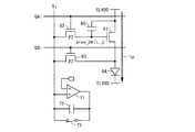
図1は、本発明の第1の実施形態に係る有機EL表示装置の構成を示すブロック図である。図1に示す有機EL表示装置1は、有機ELパネル10、表示制御回路13、走査線駆動回路14、データ線駆動回路15、および、補正データ記憶部16を備えている。有機EL表示装置1は、屈曲可能な画面を有するフレキシブル表示装置であり、画面の屈曲状態を検出する機能を有する。以下、mおよびnは2以上の整数、iは1以上n以下の整数、jは1以上m以下の整数であるとする。(First embodiment)
FIG. 1 is a block diagram showing a configuration of an organic EL display device according to the first embodiment of the present invention. The organic
図1に示すように、有機ELパネル10は、2n本の走査線GA1〜GAn、GB1〜GBn、m本のデータ線S1〜Sm、および、(m×n)個の画素回路60を含んでいる。走査線GA1〜GAn、GB1〜GBnは、互いに平行に配置される。データ線S1〜Smは、互いに平行に、走査線GA1〜GAn、GB1〜GBnと直交するように配置される。走査線GA1〜GAnとデータ線S1〜Smは、(m×n)箇所で交差する。(m×n)個の画素回路60は、(m×n)個の交差点に対応して配置される。各画素回路60は、1本の走査線と1本のデータ線とに接続される。以下、走査線GA1〜GAn、GB1〜GBnの延伸方向を行方向、データ線S1〜Smの延伸方向を列方向という。
As shown in FIG. 1, the
表示制御回路13は、有機EL表示装置1の制御回路であり、補正部80および屈曲検出部90を含んでいる。表示制御回路13には、有機EL表示装置1の外部から映像信号VS1が入力される。表示制御回路13は、走査線駆動回路14に対して制御信号CS1を出力し、データ線駆動回路15に対して制御信号CS2と映像信号VS2を出力する。制御信号CS1には、例えば、ゲートスタートパルスやゲートクロックなどが含まれる。制御信号CS2には、例えば、ソーススタートパルスやソースクロックなどが含まれる。映像信号VS2は、補正部80において映像信号VS1に対して補正処理を施すことにより得られる。補正部80と屈曲検出部90の詳細は後述する。
The
走査線駆動回路14は、走査線GA1〜GAn、GB1〜GBnを駆動することにより、画素回路60を選択する。より詳細には、走査線駆動回路14は、制御信号CS1に基づき走査線GA1〜GAnの中から1本の走査線を選択し、選択した走査線にオンレベル電圧(ここでは、ハイレベル電圧)を印加する。これにより、選択された走査線に接続されたm個の画素回路60が一括して選択される。データ線駆動回路15は、制御信号CS2と映像信号VS2に基づき、データ線S1〜Smを駆動する。より詳細には、データ線駆動回路15は、制御信号CS2に従い、映像信号VS2に応じたm個の電圧(以下、データ電圧という)をデータ線S1〜Smにそれぞれ印加する。これにより、選択されたm個の画素回路60にm個のデータ電圧がそれぞれ書き込まれる。
The scanning
データ線駆動回路15は、駆動信号生成回路17、階調信号生成回路18、および、m個の出力/測定回路(出力回路と測定回路の兼用回路)70を含んでいる。各出力/測定回路70は、データ線S1〜Smのいずれかに対応する。駆動信号生成回路17は、データ線S1〜Smを駆動するための制御信号を生成する。階調信号生成回路18は、階調信号として、データ線S1〜Smに印加されるデータ電圧を生成する。出力/測定回路70は、対応するデータ線にデータ電圧を印加する機能と、対応するデータ線を流れる電流を測定する機能とを有する。データ線に印加されたデータ電圧は、画素回路60内の駆動素子のゲート端子に書き込まれる。データ線を流れる電流は、画素回路60内の駆動素子を流れた電流である。データ線駆動回路15は、データ線を流れる電流(すなわち、画素回路60内の駆動素子を流れた電流)を測定した結果を示すモニタ信号MSを表示制御回路13に対して出力する。このようにデータ線駆動回路15は、データ線S1〜Smを駆動することにより、走査線駆動回路14によって選択された画素回路60について、駆動素子のゲート端子に電圧を書き込む動作、および、駆動素子を流れる電流を測定する動作を行う。
The data
補正部80は、モニタ信号MSに基づき画素回路60内の駆動素子と有機EL素子の特性を求め、求めた特性を用いて映像信号VS1を補正することにより映像信号VS2を求める。補正データ記憶部16は、補正部80の作業用メモリである。補正データ記憶部16は、TFTオフセット記憶部16a、TFTゲイン記憶部16b、OLEDオフセット記憶部16c、および、OLEDゲイン記憶部16dを含んでいる。TFTオフセット記憶部16aは、各画素回路60について駆動素子の閾値電圧を記憶する。TFTゲイン記憶部16bは、各画素回路60について駆動素子のゲインを記憶する。OLEDオフセット記憶部16cは、各画素回路60について有機EL素子の閾値電圧を記憶する。OLEDゲイン記憶部16dは、各画素回路60について有機EL素子のゲインを記憶する。
The
図2は、有機ELパネル10の概略構成を示す図である。図2に示すように、有機ELパネル10は、表示部11と検出部12を有する。表示部11には2〜n行目かつ1〜(m−1)列目の画素回路60が含まれ、検出部12には1行目またはm列目の画素回路60が含まれる(図1を参照)。表示部11は矩形形状を有し、検出部12は表示部11の隣接する2辺(図2では上辺と右辺)に沿って設けられる。
FIG. 2 is a diagram illustrating a schematic configuration of the
以下、表示部11に含まれる画素回路を「表示用画素回路」、検出部12に含まれる画素回路を「測定用画素回路」という。(m×n)個の画素回路60は、表示用画素回路と測定用画素回路とに分類される。本実施形態では、表示用画素回路は表示領域の内部に配置され、測定用画素回路は表示領域の外部に配置される。より詳細には、表示領域は矩形形状を有し、測定用画素回路は表示領域の隣接する2辺に沿って配置される。
Hereinafter, the pixel circuit included in the
有機ELパネル10は、プラスチック基板などを用いて、行方向および列方向に任意の位置で屈曲可能に構成される。図3は、有機ELパネル10を屈曲した状態で示す図である。図3では、有機ELパネル10は、行方向に3回屈曲している。
The
図1に示す有機ELパネル10上には、走査線GA1〜GAn、GB1〜GBn、データ線S1〜Sm、および、(m×n)個の画素回路60が形成されている。これに加えて、有機EL表示装置1に含まれる他の回路(表示制御回路13、走査線駆動回路14、データ線駆動回路15、および、補正データ記憶部16)の全部または一部を有機ELパネル10上に形成してもよい。後述する各実施形態においても、これと同様である。
On the
図4は、画素回路60と出力/測定回路70の回路図である。図4には、i行j列目の画素回路60と、データ線Sjに対応した出力/測定回路70とが記載されている。画素回路60は、トランジスタ61〜63、有機EL素子64、および、コンデンサ65を含んでいる。トランジスタ61〜63は、Nチャネル型TFTである。トランジスタ61のドレイン端子は、ハイレベル電源電位ELVDDを有するハイレベル電源線に接続される。トランジスタ61のゲート端子は、トランジスタ62の一方の導通端子(図4では右側の導通端子)に接続される。トランジスタ61のソース端子は、有機EL素子64のアノード端子とトランジスタ63の一方の導通端子(図4では右側の導通端子)とに接続される。有機EL素子64のカソード端子は、ローレベル電源電位ELVSSを有するローレベル電源線に接続される。トランジスタ62、63の他方の導通端子は、データ線Sjに接続される。トランジスタ62のゲート端子は走査線GAiに接続され、トランジスタ63のゲート端子は走査線GBiに接続される。コンデンサ65は、トランジスタ61のドレイン端子とゲート端子の間に設けられる。トランジスタ61は駆動素子として機能し、有機EL素子64は発光素子として機能する。
FIG. 4 is a circuit diagram of the
出力/測定回路70は、オペアンプ71、コンデンサ72、および、スイッチ73を含んでいる。オペアンプ71の非反転入力端子には、階調信号生成回路18に含まれるD/A変換回路(図示せず)から出力されたデータ電圧DVjが印加される。オペアンプ71の反転入力端子は、データ線Sjに接続される。コンデンサ72の一端はオペアンプ71の反転入力端子に接続され、コンデンサ72の他端はオペアンプ71の出力端子に接続される。同様に、スイッチ73の一端はオペアンプ71の反転入力端子に接続され、スイッチ73の他端はオペアンプ71の出力端子に接続される。このようにコンデンサ72とスイッチ73は、オペアンプ71の反転入力端子と出力端子との間に並列に設けられる。
The output /
スイッチ73がオン状態のときには、オペアンプ71はバッファアンプとして機能する。このとき、オペアンプ71の非反転入力端子と反転入力端子は仮想短絡され、データ線Sjにはオペアンプ71の非反転入力端子に印加されたデータ電圧DVjが印加される。スイッチ73がオフ状態のときには、オペアンプ71とコンデンサ72は積分アンプとして機能する。このとき、オペアンプ71の出力電圧は、データ線Sjを流れる電流の量に応じて変化する。このように出力/測定回路70は、スイッチ73の状態に応じて、データ電圧をデータ線Sjに印加する動作と、データ線Sjを流れる電流を測定する動作とを選択的に行う。
When the
有機EL表示装置1は、1フレーム期間に1行の画素回路60について電流を測定する。以下、あるフレーム期間において電流測定の対象となる行を測定対象行、それ以外の行を通常行という。測定対象行は、フレーム期間ごとに切り替えられる。i行目が通常行である場合、走査線駆動回路14は走査線GAiにオンレベル電圧を印加し、データ線駆動回路15はi行目の画素回路60に書き込むべきm個のデータ電圧をデータ線S1〜Smに印加する。i行目が測定対象行である場合、走査線駆動回路14とデータ線駆動回路15は、図5に示すように走査線GAi、GBiとデータ線S1〜Smを駆動する。
The organic
図5は、有機EL表示装置1のタイミングチャートである。図5には、i行目が測定対象行である場合について、走査線GAi、GBiとデータ線Sjの電位の変化が記載されている。図5において、期間T1〜T3はi行目の画素回路60の電流測定期間であり、期間T4はi行目の画素回路60の電流測定期間後の電圧書き込み期間である。図6A〜図6Eは、図4に示す回路の動作を示す図である。以下、図5および図6A〜図6Eを参照して、図4に示す回路の動作を説明する。
FIG. 5 is a timing chart of the organic
期間T1より前では、走査線GAi、GBiの電位はローレベルである。このとき、トランジスタ62、63はオフ状態にある(図6Aを参照)。トランジスタ61のゲート電圧は、コンデンサ65の作用によって、前回書き込まれたデータ電圧prev_DV(i,j)に保たれる。トランジスタ61はオン状態であり、トランジスタ61と有機EL素子64にはトランジスタ61のゲート−ソース間電圧に応じた電流Ipが流れる。有機EL素子64は、前回のデータ電圧prev_DV(i,j)に応じた輝度で発光する。
Prior to the period T1, the potentials of the scanning lines GAi and GBi are at a low level. At this time, the
期間T1では、走査線GAiの電位はハイレベルになる。このため、トランジスタ62はオン状態になる(図6Bを参照)。また、期間T1では、スイッチ73はオン状態になり、オペアンプ71の非反転入力端子にはリファレンス電圧Vmgが印加される。オペアンプ71はバッファアンプとして機能するので、データ線Sjにはリファレンス電圧Vmgが印加され、トランジスタ61のゲート電圧はVmgになる。
In the period T1, the potential of the scanning line GAi is at a high level. Therefore, the
期間T2では、走査線GAiの電位はローレベルになり、走査線GBiの電位はハイレベルになる。このため、トランジスタ62はオフ状態になり、トランジスタ63はオン状態になる(図6Cを参照)。また、期間T2では、スイッチ73はオフ状態になり、オペアンプ71の非反転入力端子にはトランジスタ61の特性を求めるための第1測定用電圧Vm_TFTが印加される。第1測定用電圧Vm_TFTは、このときにハイレベル電源線からトランジスタ61とトランジスタ63を経由して出力/測定回路70に電流Iaが流れるように決定される。オペアンプ71とコンデンサ72は積分アンプとして機能し、オペアンプ71は電流Iaに応じた電圧Vmaを出力する。電圧Vmaを電流値に変換することにより、期間T2にトランジスタ61を流れる電流Iaを測定することができる。
In the period T2, the potential of the scan line GAi is at a low level, and the potential of the scan line GBi is at a high level. Therefore, the
期間T3では、オペアンプ71の非反転入力端子には有機EL素子64の特性を求めるための第2測定用電圧Vm_OLEDが印加される(図6Dを参照)。第2測定用電圧Vm_OLEDは、このときに出力/測定回路70からトランジスタ63と有機EL素子64を通過してローレベル電源線に電流Ibが流れるように決定される。オペアンプ71とコンデンサ72は積分アンプとして機能し、オペアンプ71は電流Ibに応じた電圧Vmbを出力する。電圧Vmbを電流値に変換することにより、期間T3に有機EL素子64を流れる電流Ibを測定することができる。
In the period T3, the second measurement voltage Vm_OLED for obtaining the characteristics of the
期間T4では、走査線GAiの電位はハイレベルになり、走査線GBiの電位はローレベルになる。このため、トランジスタ62はオン状態になり、トランジスタ63はオフ状態になる(図6Eを参照)。また、期間T4では、スイッチ73はオン状態になり、オペアンプ71の非反転入力端子には新たなデータ電圧DV(i,j)が印加される。オペアンプ71はバッファアンプとして機能するので、データ線Sjにはデータ電圧DV(i,j)が印加され、トランジスタ62のゲート電圧はDV(i,j)になる。
In the period T4, the potential of the scan line GAi is at a high level, and the potential of the scan line GBi is at a low level. Therefore, the
期間T4以降、走査線GAi、GBiの電位はローレベルになる。したがって、期間T1より前と同様に、有機EL素子64にはトランジスタ61のゲート−ソース間電圧に応じた電流Icが流れる。有機EL素子64は、期間T4で書き込まれたデータ電圧DV(i,j)に応じた輝度で発光する。
After the period T4, the potentials of the scanning lines GAi and GBi become low level. Accordingly, the current Ic corresponding to the gate-source voltage of the
期間T2では、トランジスタ61のゲート端子にリファレンス電圧Vmgを印加し、トランジスタ61のソース端子に第1測定用電圧Vm_TFTを印加したときに、トランジスタ61を流れる電流Iaが測定される。期間T3では、有機EL素子64のアノード端子に第2測定用電圧Vm_OLEDを印加したときに、有機EL素子64を流れる電流Ibが測定される。
In the period T2, the current Ia flowing through the
なお、図5に示すタイミングチャートでは、電流測定期間T1〜T3の後に電圧書き込み期間T4を設け、有機EL素子64は、期間T4以降において発光することとした。これに代えて、電流測定期間T1〜T3の後に黒書き込み期間を設け、有機EL素子64は期間T4以降において発光しないこととしてもよい。
In the timing chart shown in FIG. 5, the voltage writing period T4 is provided after the current measurement periods T1 to T3, and the
以下、補正部80について説明する。上述したように、データ線駆動回路15は、データ線を流れる電流を測定した結果を示すモニタ信号MSを表示制御回路13に対して出力する。補正部80は、各画素回路60について、トランジスタ61を流れる電流Iaを測定した結果(具体的には、期間T2におけるオペアンプ71の出力電圧Vmaを測定した結果を電流値に変換した結果)に基づき、トランジスタ61の閾値電圧とゲインを求める。求めた閾値電圧とゲインは、それぞれ、TFTオフセット記憶部16aとTFTゲイン記憶部16bに記憶される。また、補正部80は、各画素回路60について、有機EL素子64を流れる電流Ibを測定した結果(具体的には、期間T3におけるオペアンプ71の出力電圧Vmbを測定した結果を電流値に変換した結果)に基づき、有機EL素子64の閾値電圧とゲインを求める。求めた閾値電圧とゲインは、それぞれ、OLEDオフセット記憶部16cとOLEDゲイン記憶部16dに記憶される。
Hereinafter, the
補正部80は、電流Iaの測定結果に基づき、任意の方法でトランジスタ61の閾値電圧とゲインを求めてもよく、電流Ibの測定結果に基づき、任意の方法で有機EL素子64の閾値電圧とゲインを求めてもよい。例えば、補正部80は、各画素回路60について、相対的に低い第1測定用電圧を印加したときの電流Iaと、相対的に高い第1測定用電圧を印加したときの電流Iaとを測定し、閾値電圧とゲインを未知数とした方程式を解くことにより、トランジスタ61の閾値電圧とゲインを求めてもよい。あるいは、補正部80は、各画素回路60について、相対的に低い第1測定用電圧を印加したときの電流Iaの測定結果と電流Iaの理想値との比較結果に応じてTFTオフセット記憶部16aに記憶されたトランジスタ61の閾値電圧を更新し、相対的に高い第1測定用電圧を印加したときの電流Iaの測定結果と電流Iaの理想値との比較結果に応じてTFTゲイン記憶部16bに記憶されたトランジスタ61のゲインを更新してもよい。
The correcting
図7は、補正部80における補正処理を説明するための図である。図7に示すように、補正部80は、ルックアップテーブル(Look Up Table :以下、LUTという)81、乗算器82、83、86、および、加算器84、85を含んでいる。以下、映像信号VS1に含まれる、ある画素の階調データP1に対する処理を説明する。ここでは、この画素に対応する画素回路をPXという。
FIG. 7 is a diagram for explaining correction processing in the
LUT81は、階調データP1に対してガンマ補正を行う。乗算器82は、ガンマ補正後の階調データに、TFTゲイン記憶部16bから読み出された、画素回路PX内のトランジスタ61のゲインを乗算する。乗算器83は、乗算器82の出力に、OLEDゲイン記憶部16dから読み出された、画素回路PX内の有機EL素子64のゲインを乗算する。加算器84は、乗算器83の出力に、TFTオフセット記憶部16aから読み出された、画素回路PX内のトランジスタ61の閾値電圧を加算する。加算器85は、加算器84の出力に、OLEDオフセット記憶部16cから読み出された、画素回路PX内の有機EL素子64の閾値電圧を加算する。乗算器86は、加算器85の出力に、データ電圧の減衰を補償するための係数Zを乗算する。乗算器86の出力は、階調データP1に対して補正処理を施した補正後の階調データP2となる。表示制御回路13から出力される映像信号VS2には、補正後の階調データP2が含まれる。
The
以下、屈曲検出部90について説明する。上述したように、補正部80は、有機ELパネル10に含まれる画素回路60について、トランジスタ61の閾値電圧とゲインを求める。この処理は、表示部11に含まれる表示用画素回路だけでなく、検出部12に含まれる測定用画素回路についても行われる。有機ELパネル10が屈曲したとき、測定用画素回路内のトランジスタ61のチャネル領域(ドレイン/ソース電極とゲート電極が平面視で重なる領域)は変形する。これに伴い、測定用画素回路内のトランジスタ61の電気的特性(閾値電圧やI−V特性)は変化し、測定用画素回路内のトランジスタ61を流れる電流の量は変化する。そこで、屈曲検出部90は、測定用画素回路内のトランジスタ61を流れる電流量の変化に基づき、有機ELパネル10の屈曲状態を検出する。
Hereinafter, the bending
屈曲検出部90は、各測定用画素回路について、トランジスタ61の閾値電圧の初期値Vth0とゲインの初期値β0とを記憶している。ここで、初期値とは、有機EL表示装置1に電源が投入された後に最初に求められた値をいう。補正部80は、測定用画素回路内のトランジスタ61の閾値電圧Vthとゲインβを求めたときに、これらの値を屈曲検出部90に対して出力する。屈曲検出部90は、閾値電圧の初期値Vth0と新たに求められた閾値電圧Vthとの差ΔVth(=Vth−Vth0)、および、ゲインの初期値β0と新たに求められたゲインβとの差Δβ(=β−β0)を求める。屈曲検出部90は、求めた差ΔVth、Δβに基づき、測定用画素回路の位置における有機ELパネル10の屈曲状態を求める。屈曲検出部90は、有機ELパネル10が屈曲しているか否かを求めてもよく、有機ELパネル10が屈曲している程度を段階的に示す値を求めてもよく、有機ELパネル10の屈曲量を数値として求めてもよい。屈曲検出部90は、検出した屈曲状態を補正部80に対して出力する。
The bending
補正部80は、屈曲検出部90で検出された屈曲状態に基づき、映像信号VS1を補正する。より詳細には、補正部80は、屈曲検出部90で検出された屈曲状態に基づき、表示用画素回路内のトランジスタ61を流れる電流量の屈曲による変化を補償するように映像信号VS1を補正する。例えば、屈曲検出部90は、差ΔVth、Δβの値の組合せに対応して有機ELパネル10の曲率を記憶した曲率LUTを内蔵しており、求めた差ΔVth、Δβを用いて曲率LUTを参照することにより、測定用画素回路の位置における有機ELパネル10の曲率を求める。補正部80は、曲率に対応してトランジスタ61の閾値電圧とゲインの補正量を記憶した補正LUTを内蔵しており、補正部80で求めた曲率を用いて補正LUTを参照することにより、トランジスタ61の閾値電圧とゲインの補正量を求め、求めた補正量を用いて映像信号VS1を補正する。このようにして映像信号VS1を補正することにより、画面屈曲時の輝度や色の変化を防止することができる。あるいは、補正部80は、屈曲検出部90で検出された屈曲状態に基づき、屈曲部分に対応した映像信号VS1を非表示レベル(例えば、黒レベル)に補正してもよい。これにより、画面屈曲時の輝度や色の変化を隠すことができる。
The correcting
屈曲検出部90で検出された屈曲状態は、上記以外にも利用することができる。例えば、有機ELパネルがタッチパネル機能を有する場合、表示制御回路は、有機ELパネルが屈曲していることを検出したときに、タッチパネル機能を停止してもよい。
The bending state detected by the bending
以上に示すように、本実施形態に係る有機EL表示装置1は、複数の走査線GA1〜GAn、GB1〜GBnと、複数のデータ線S1〜Smと、それぞれが発光素子(有機EL素子64)および駆動素子(トランジスタ61)を有する複数の画素回路60とを含む屈曲可能な表示パネル(有機ELパネル10)と、走査線GA1〜GAn、GB1〜GBnを駆動することにより、画素回路60を選択する走査線駆動回路14と、データ線S1〜Smを駆動することにより、走査線駆動回路14によって選択された画素回路60について、駆動素子の制御端子(トランジスタ61のゲート端子)に電圧を書き込む動作、および、駆動素子を流れる電流を測定する動作を行うデータ線駆動回路15と、駆動素子を流れる電流Iaを測定した結果に基づき、表示パネルの屈曲状態を検出する屈曲検出部90とを備えている。本実施形態に係る有機EL表示装置1によれば、画面屈曲時に駆動素子の電気的特性が変化するので、駆動素子を流れる電流を測定した結果に基づき画面の屈曲状態を検出することができる。
As described above, the organic
また、画素回路60は、表示用画素回路(表示部11に含まれる画素回路)と測定用画素回路(検出部12に含まれる画素回路)とに分類され、屈曲検出部90は、測定用画素回路内の駆動素子を流れる電流を測定した結果に基づき、表示パネルの屈曲状態を検出する。このように表示用画素回路とは別に測定用画素回路を設け、測定用画素回路内の駆動素子を流れる電流を測定した結果に基づき画面の屈曲状態を検出することができる。また、表示用画素回路は表示領域の内部に配置され、測定用画素回路は表示領域の外部に配置されている。このように表示用画素回路を配置した表示領域の外部に測定用画素回路を配置することにより、表示に影響を与えることなく画面の屈曲状態を検出することができる。また、表示領域は矩形形状を有し、測定用画素回路は表示領域の隣接する2辺に沿って配置されている。これにより、画面がいずれの方向に屈曲したときでも画面の屈曲状態を検出することができる。
The
また、有機EL表示装置1は屈曲検出部90で検出された屈曲状態に基づき映像信号VS1を補正する補正部80を備え、データ線駆動回路15は補正部80で補正された映像信号VS2に基づく電圧をデータ線S1〜Smに印加する。このように検出した屈曲状態に基づき映像信号VS1を補正することにより、画面屈曲時の輝度や色の変化を防止することができる。補正部80は、駆動素子を流れる電流量の屈曲による変化を補償するように映像信号VS1を補正してもよい。映像信号を補正して駆動素子を流れる電流量の屈曲による変化を補償することにより、画面屈曲時の輝度や色の変化を防止することができる。また、補正部80は、屈曲部分に対応した映像信号VS1を非表示レベルに補正してもよい。このように映像信号VS1を補正して屈曲部分を非表示にすることにより、画面屈曲時の輝度や色の変化を隠すことができる。
The organic
なお、有機EL表示装置1では、表示領域の2辺に沿って測定用画素回路を配置することとした。これに代えて、図8に示すように、表示領域の1辺に沿って測定用画素回路を配置してもよい。図8に示す有機ELパネル100では、表示部101は矩形形状を有し、検出部102は表示部101の1辺(図8では上辺)に沿って設けられる。表示部101には2〜n行目の画素回路が含まれ、検出部12には1行目の画素回路が含まれる。このように測定用画素回路を1方向に沿って配置することにより、測定用画素回路が並ぶ方向に画面が屈曲したときに画面の屈曲状態を検出することができる。
In the organic
(第2の実施形態)
図9は、本発明の第2の実施形態に係る有機EL表示装置の構成を示すブロック図である。図9に示す有機EL表示装置2は、第1の実施形態に係る有機EL表示装置1において、有機ELパネル10を有機ELパネル20に置換したものである。以下、各実施形態の構成要素のうち、第1の実施形態と同一の要素については、同一の参照符号を付して説明を省略する。(Second Embodiment)
FIG. 9 is a block diagram showing a configuration of an organic EL display device according to the second embodiment of the present invention. An organic
有機ELパネル20は、以下の点で、有機ELパネル10と相違する。有機ELパネル20は、表示部21と検出部22を有する。表示部21には2〜n行目かつ1〜(m−2)列目の画素回路60が含まれ、検出部22には1行目または(m−1)〜m列目の画素回路60が含まれる。m列目の画素回路60は、(m−1)列目の画素回路60から1/2行だけずれた位置(図9では下方向にずれた位置)に配置される。このように有機EL表示装置2では、測定用画素回路の配置態様は、表示用画素回路の配置態様と異なる。また、測定用画素回路の配置間隔は、表示用画素回路の配置間隔と異なり、表示用画素回路の配置間隔の半分である。
The
第1の実施形態に係る有機EL表示装置1では、測定用画素回路は表示用画素回路と同じ態様に配置されている。具体的には、有機EL表示装置1では、測定用画素回路は1列に表示用画素回路と同じ配置間隔で配置されている。有機EL表示装置1によれば、表示用画素回路の配置間隔の精度で有機ELパネル10の屈曲状態を求めることができる。
In the organic
これに対して有機EL表示装置2では、測定用画素回路は2列に配置され、2列の測定用画素回路は表示用画素回路の配置間隔の1/2行だけずれた位置に配置されている。具体的には、(m−1)列目の画素回路60は表示用画素回路と同じ態様に配置され、m列目の画素回路60は表示用画素回路から1/2行だけずれた位置に配置されている。したがって、有機EL表示装置2によれば、有機EL表示装置1よりも高い精度で(表示用画素回路の配置間隔の1/2の精度で)、有機ELパネル20の屈曲状態を求めることができる。
On the other hand, in the organic
以上に示すように、本実施形態に係る有機EL表示装置2では、測定用画素回路の配置態様(配置間隔)は、表示用画素回路の配置態様と異なる。有機EL表示装置2によれば、表示用画素回路と測定用画素回路を異なる態様(異なる間隔)で配置することにより、画面の屈曲状態を高い精度で検出することができる。
As described above, in the organic
なお、有機ELパネル20は、1行の測定用画素回路と2列の測定用画素回路とを含むこととした。これに代えて、有機ELパネルは、任意の数の行の測定用画素回路を含んでもよく、任意の数の列の測定用画素回路を含んでもよい。有機ELパネルがp行(pは2以上の整数)の測定用画素回路を含む場合、p行の測定用画素回路は行ごとに1/p列だけずれた位置に配置される。有機ELパネルがq列(qは2以上の整数)の測定用画素回路を含む場合、q列の測定用画素回路は列ごとに1/q行だけずれた位置に配置される。測定用画素回路の行数や列数が多いほど、有機ELパネルの屈曲状態を高い精度で検出することができる。
The
(第3の実施形態)
図10は、本発明の第3の実施形態に係る有機EL表示装置の構成を示すブロック図である。図10に示す有機EL表示装置3は、第1の実施形態に係る有機EL表示装置1において、有機ELパネル10を有機ELパネル30に置換したものである。(Third embodiment)
FIG. 10 is a block diagram showing a configuration of an organic EL display device according to the third embodiment of the present invention. An organic
有機ELパネル30は、以下の点で、有機ELパネル10と相違する。有機ELパネル30は、表示部31と検出部32を有する。表示部31には奇数列目の画素回路60が含まれ、検出部32には偶数列目の画素回路60が含まれる。このように本実施形態に係る有機EL表示装置3では、表示領域は矩形形状を有し、表示用画素回路と測定用画素回路とは表示領域の内部に混在して配置されている。言い換えると、測定用画素回路は、表示用画素回路と共に、矩形形状を有する表示領域の内部に配置されている。有機EL表示装置3によれば、画面の局所的な屈曲を検出することができる。
The
なお、有機ELパネル30では、1列の画素回路60を含む表示部31と1列の画素回路60を含む検出部32とが行方向に交互に配置されている。これに代えて、任意の数の列の画素回路60を含む表示部と任意の数の列の画素回路60を含む検出部とを行方向に交互に配置してもよい。また、任意の数の行の画素回路60を含む表示部と任意の数の行の画素回路60を含む検出部とを列方向に交互に配置してもよい。
In the
(第4の実施形態)
図11は、本発明の第4の実施形態に係る有機EL表示装置の構成を示すブロック図である。図11に示す有機EL表示装置4は、第1の実施形態に係る有機EL表示装置1において、有機ELパネル10を有機ELパネル40に置換したものである。(Fourth embodiment)
FIG. 11 is a block diagram showing a configuration of an organic EL display device according to the fourth embodiment of the present invention. An organic
有機ELパネル40は、以下の点で、有機ELパネル10と相違する。図12は、有機ELパネル40の概略構成を示す図である。図11および図12に示すように、有機ELパネル40は、表示部41が形成された層(以下、表示層43という)と、検出部42が形成された層(以下、検出層44という)とを含む多層構造(2層構造)を有する。有機ELパネル30と同様に、表示部41には奇数列目の画素回路60が含まれ、検出部42には偶数列目の画素回路60が含まれる。表示層43と検出層44は別々に形成され、有機ELパネル40は表示層43と検出層44を張り合わせることにより形成される。
The
後述する第5の実施形態のように、表示用画素回路と測定用画素回路の間で駆動素子のサイズや種類を異ならせる場合に、2種類の画素回路を同じ層に形成すると、画素回路の形成に用いる材料が混じるなどの問題が発生することがある。有機EL表示装置4では、表示用画素回路と測定用画素回路が異なる層に形成されるので、2種類の画素回路を同じ層に形成するときの問題が発生しない。また、一方の層に不良が発生した場合に、不良が発生した層だけを変更することにより、有機ELパネル40の歩留まりを向上させ、有機EL表示装置4のコストを低減することができる。
As in the fifth embodiment to be described later, when different sizes and types of driving elements are used between the display pixel circuit and the measurement pixel circuit, if two types of pixel circuits are formed in the same layer, the pixel circuit Problems such as mixing of materials used for formation may occur. In the organic
以上に示すように、本実施形態に係る有機EL表示装置4では、表示パネル(有機ELパネル40)は、表示用画素回路が形成された層(表示層43)と、測定用画素回路が形成された層(検出層44)とを含む多層構造を有する。有機EL表示装置4によれば、表示用画素回路と測定用画素回路を異なる層に形成することにより、2種類の画素回路を同じ層に形成するときの問題を解決することができる。
As described above, in the organic
(第5の実施形態)
本発明の第5の実施形態に係る有機EL表示装置は、第1〜第4の実施形態に係る有機EL表示装置1〜4のいずれかと同じ構成を有する。本実施形態に係る有機EL表示装置は、測定用画素回路内の駆動素子の電気的特性が、表示用画素回路内の駆動素子の電気的特性と異なることを特徴とする。(Fifth embodiment)
The organic EL display device according to the fifth embodiment of the present invention has the same configuration as any one of the organic
本実施形態に係る有機EL表示装置では、表示用画素回路内の駆動素子には、画面屈曲時に電流量の変化が小さい(より好ましくは、電流量が変化しない)トランジスタが使用される。一方、測定用画素回路内の駆動素子には、画面屈曲時に電流量の変化が大きいトランジスタが使用される。 In the organic EL display device according to this embodiment, a transistor having a small change in current amount (more preferably, the current amount does not change) is used as a drive element in the display pixel circuit when the screen is bent. On the other hand, a transistor having a large change in the amount of current when the screen is bent is used as a drive element in the measurement pixel circuit.
例えば、測定用画素回路内の駆動素子として、表示用画素回路内の駆動素子とは異なるサイズのトランジスタ(表示用画素回路内の駆動素子よりも大きいトランジスタ)を用いてもよい。具体的には、測定用画素回路内の駆動素子として、表示用画素回路内の駆動素子よりもチャネル長が短いトランジスタや、表示用画素回路内の駆動素子よりもチャネル幅が長いトランジスタを用いることができる。あるいは、測定用画素回路内の駆動素子として、表示用画素回路内の駆動素子とは異なる種類のトランジスタ(例えば、有機TFT)を用いてもよい。具体的には、表示用画素回路内の駆動素子をアモルファスシリコンや結晶型シリコンを用いて形成し、測定用画素回路内の駆動素子をオフ電流の小さい酸化物半導体を用いて形成することができる。 For example, a transistor having a different size from the drive element in the display pixel circuit (a transistor larger than the drive element in the display pixel circuit) may be used as the drive element in the measurement pixel circuit. Specifically, a transistor having a channel length shorter than that of the driving element in the display pixel circuit or a transistor having a channel width longer than that of the driving element in the display pixel circuit is used as the driving element in the measurement pixel circuit. Can do. Alternatively, a different type of transistor (for example, organic TFT) from the drive element in the display pixel circuit may be used as the drive element in the measurement pixel circuit. Specifically, the drive element in the display pixel circuit can be formed using amorphous silicon or crystalline silicon, and the drive element in the measurement pixel circuit can be formed using an oxide semiconductor with a small off-state current. .
以上に示すように、本実施形態に係る有機EL表示装置では、測定用画素回路内の駆動素子の電気的特性(サイズ、種類)は、表示用画素回路内の駆動素子の電気的特性(サイズ、種類)と異なる。したがって、画面の屈曲状態を高い精度で検出することができる。 As described above, in the organic EL display device according to the present embodiment, the electrical characteristics (size, type) of the drive element in the measurement pixel circuit are the same as the electrical characteristics (size) of the drive element in the display pixel circuit. , Kind) and different. Therefore, the bent state of the screen can be detected with high accuracy.
(第6の実施形態)
図13は、本発明の第6の実施形態に係る有機EL表示装置の構成を示すブロック図である。図13に示す有機EL表示装置5は、第1の実施形態に係る有機EL表示装置1において、有機ELパネル10と表示制御回路13を、それぞれ、有機ELパネル50と表示制御回路19に置換したものである。表示制御回路19は、表示制御回路13において、補正部80と屈曲検出部90を、それぞれ、補正部89と屈曲検出部99に置換したものである。(Sixth embodiment)
FIG. 13 is a block diagram showing a configuration of an organic EL display device according to the sixth embodiment of the present invention. In the organic EL display device 5 shown in FIG. 13, in the organic
有機ELパネル50は、表示部51を有し、検出部を有しない点で、有機ELパネル10と相違する。表示部51には、有機ELパネル50に含まれるすべての画素回路60が含まれる。
The
補正部89は、各表示用画素回路について、トランジスタ61の閾値電圧とゲインを求める。屈曲検出部99は、各表示用画素回路について、トランジスタ61の閾値電圧の初期値Vth0とゲインの初期値β0とを記憶している。補正部89は、表示用画素回路内のトランジスタ61の閾値電圧Vthとゲインβを求めたときに、これらの値を屈曲検出部99に対して出力する。屈曲検出部99は、閾値電圧の初期値Vth0と新たに求められた閾値電圧Vthとの差ΔVth、および、ゲインの初期値β0と新たに求められたゲインβとの差Δβを求める。屈曲検出部99は、求めた差ΔVth、Δβが大きいときに、表示用画素回路の位置における有機ELパネル50の屈曲状態を求める。補正部89は、第1の実施形態に係る補正部80と同様に、屈曲検出部90で検出された屈曲状態に基づき、映像信号VS1を補正する。
The
あるいは、補正部89は、トランジスタ61の電気的特性(以下、第1特性という)と有機EL素子64の電気的特性(以下、第2特性という)とを求め、屈曲検出部99は、第2特性に基づき有機ELパネル50が屈曲していないときのトランジスタ61の電気的特性(以下、第3特性という)を推定し、第1特性と第3特性とを比較することにより、有機ELパネル50の屈曲状態を検出してもよい。
Alternatively, the
具体的には、屈曲検出部99は、上述した曲率LUTに加えて、2種類のエージングLUT(トランジスタのエージングLUTと有機EL素子のエージングLUT)を内蔵する。有機EL素子のエージングLUTは、期間T3におけるオペアンプ71の出力電圧Vmbに対応してエージング時間を記憶している。トランジスタのエージングLUTは、エージング時間に対応してトランジスタの閾値電圧とゲインを記憶している。屈曲検出部99は、まず、期間T3で測定された電圧Vmbを用いて有機EL素子のエージングLUTを参照することによりエージング時間を求める。次に、屈曲検出部99は、求めたエージング時間を用いてトランジスタのエージングLUTを参照することにより、有機ELパネル50が屈曲していないときのトランジスタ61の閾値電圧とゲインを推定する。さらに、屈曲検出部99は、期間T2で測定された電圧Vmaに基づくトランジスタ61の閾値電圧およびゲインと、2種類のエージングLUTを用いて推定したトランジスタ61の閾値電圧およびゲインとを比較することにより、有機ELパネル50の屈曲状態を検出する。この場合も、補正部89は、屈曲検出部90で検出された屈曲状態に基づき、映像信号VS1を補正する。
Specifically, the
以上に示すように、本実施形態に係る有機EL表示装置5では、有機ELパネル50は表示用画素回路(表示部51に含まれる画素回路)だけを含み、屈曲検出部90は、表示用画素回路内の駆動素子を流れる電流を測定した結果に基づき、表示パネルの屈曲状態を検出する。有機EL表示装置5によれば、表示用画素回路を測定用画素回路としても用いることにより、有機ELパネル50の歩留まりを向上させ、有機EL表示装置のコストを低減することができる。
As described above, in the organic EL display device 5 according to the present embodiment, the
なお、第1〜第6の実施形態に係る有機EL表示装置は、1フレーム期間に1行の画素回路60について電流を測定することとした。これに代えて、本発明の有機EL表示装置は、1フレーム期間に複数行の画素回路60について、電流を行ごとに順に測定してもよい。また、本発明の有機EL表示装置は、複数行の画素回路60を一括して選択し、複数の画素回路60からデータ線に流れる電流を測定してもよい。また、第1〜第6の実施形態に係る有機EL表示装置では、表示領域は矩形形状を有することとした。これに代えて、本発明の有機EL表示装置では、表示領域は矩形以外の形状(例えば、楕円形状やひし形形状)を有していてもよい。
In the organic EL display devices according to the first to sixth embodiments, current is measured for one row of
また、第1〜第6の実施形態では、例として、画素回路60と出力/測定回路70とを含む有機EL表示装置について説明した。本発明は、他の画素回路と他の電流測定回路とを含む有機EL表示装置にも適用することができる。また、本発明は、有機EL表示装置以外のフレキシブル表示装置にも適用することができる。
In the first to sixth embodiments, the organic EL display device including the
なお、本願は、2015年12月2日に出願された「フレキシブル表示装置およびその屈曲状態検出方法」という名称の日本国特願2015−235388号に基づく優先権を主張する出願であり、この出願の内容は引用することによって本願の中に含まれる。 In addition, this application is an application which claims priority based on Japanese Patent Application No. 2015-235388 entitled “Flexible Display Device and its Bending State Detection Method” filed on December 2, 2015. Is incorporated herein by reference.
本発明の表示装置は、画面の屈曲状態を検出し、画面屈曲時の輝度や色の変化を防止できるという特徴を有するので、有機EL表示装置を始め、各種のフレキシブル表示装置に利用することができる。 Since the display device of the present invention has a feature that it can detect the bending state of the screen and prevent changes in luminance and color when the screen is bent, it can be used for various flexible display devices including organic EL display devices. it can.
1、2、3、4、5…有機EL表示装置
10、20、30、40、50、100…有機ELパネル
11、21、31、41、51、101…表示部
12、22、32、42、102…検出部
13、19…表示制御回路
14…走査線駆動回路
15…データ線駆動回路
16…補正データ記憶部
43…表示層
44…検出層
60…画素回路
61…トランジスタ(駆動素子)
64…有機EL素子(発光素子)
70…出力/測定回路
80、89…補正部
90、99…屈曲検出部1, 2, 3, 4, 5 ... Organic
64. Organic EL element (light emitting element)
70: Output /
Claims (13)
前記走査線を駆動することにより、前記画素回路を選択する走査線駆動回路と、
前記データ線を駆動することにより、前記走査線駆動回路によって選択された画素回路について、前記駆動素子の制御端子に電圧を書き込む動作、および、前記駆動素子を流れる電流を測定する動作を行うデータ線駆動回路と、
屈曲検出部とを備え、
前記画素回路は、表示用画素回路と測定用画素回路とに分類され、
前記屈曲検出部は、前記測定用画素回路内の駆動素子を流れる電流を測定した結果に基づき、前記表示パネルの屈曲状態を検出し、
前記測定用画素回路の配置間隔は、前記表示用画素回路の配置間隔よりも狭いことを特徴とする、フレキシブル表示装置。 A bendable display panel including a plurality of scanning lines, a plurality of data lines, and a plurality of pixel circuits each having a light emitting element and a driving element;
A scanning line driving circuit for selecting the pixel circuit by driving the scanning line;
A data line that performs an operation of writing a voltage to a control terminal of the drive element and an operation of measuring a current flowing through the drive element for the pixel circuit selected by the scanning line drive circuit by driving the data line A drive circuit;
A bending detection unit,
The pixel circuit is classified into a display pixel circuit and a measurement pixel circuit,
The bending detection unit detects a bending state of the display panel based on a result of measuring a current flowing through a driving element in the measurement pixel circuit,
The flexible display device, wherein an arrangement interval of the measurement pixel circuits is narrower than an arrangement interval of the display pixel circuits.
前記走査線を駆動することにより、前記画素回路を選択する走査線駆動回路と、
前記データ線を駆動することにより、前記走査線駆動回路によって選択された画素回路について、前記駆動素子の制御端子に電圧を書き込む動作、および、前記駆動素子を流れる電流を測定する動作を行うデータ線駆動回路と、
屈曲検出部とを備え、
前記画素回路は、複数の表示用画素回路と複数の測定用画素回路とに分類され、
前記屈曲検出部は、前記測定用画素回路内の駆動素子を流れる電流を測定した結果に基づき、前記表示パネルの屈曲状態を検出し、
前記表示パネルは、複数の前記表示用画素回路が形成された層と、複数の前記測定用画素回路が形成された層とを含む多層構造を有し、
複数の前記測定用画素回路は、それぞれ、前記複数の走査線のうち対応する走査線に接続され、
少なくとも一つの前記表示用画素回路に接続された走査線と、少なくとも一つの前記測定用画素回路に接続された対応する走査線とは、電気的に接続されていることを特徴とする、フレキシブル表示装置。 A bendable display panel including a plurality of scanning lines, a plurality of data lines, and a plurality of pixel circuits each having a driving element;
A scanning line driving circuit for selecting the pixel circuit by driving the scanning line;
A data line that performs an operation of writing a voltage to a control terminal of the drive element and an operation of measuring a current flowing through the drive element for the pixel circuit selected by the scanning line drive circuit by driving the data line A drive circuit;
A bending detection unit,
The pixel circuit is classified into a plurality of display pixel circuits and a plurality of measurement pixel circuits.
The bending detection unit detects a bending state of the display panel based on a result of measuring a current flowing through a driving element in the measurement pixel circuit,
The display panel has a multilayer structure including a layer in which a plurality of display pixel circuits are formed and a layer in which the plurality of measurement pixel circuits are formed,
Each of the plurality of measurement pixel circuits is connected to a corresponding scanning line among the plurality of scanning lines,
A flexible display, wherein a scanning line connected to at least one display pixel circuit and a corresponding scanning line connected to at least one measurement pixel circuit are electrically connected. apparatus.
前記走査線を駆動することにより、前記画素回路を選択する走査線駆動回路と、
前記データ線を駆動することにより、前記走査線駆動回路によって選択された画素回路について、前記駆動素子の制御端子に電圧を書き込む動作、および、前記駆動素子を流れる電流を測定する動作を行うデータ線駆動回路と、
前記駆動素子を流れる電流を測定した結果に基づき、前記表示パネルの屈曲状態を検出する屈曲検出部と、
前記屈曲検出部で検出された屈曲状態に基づき、前記駆動素子を流れる電流量の屈曲による変化を補償するように映像信号を補正する補正部とを備え、
前記データ線駆動回路は、前記補正部で補正された映像信号に基づく電圧を前記データ線に印加し、
前記屈曲検出部は、前記駆動素子の電気的特性の初期値との差に対応して前記表示パネルの曲率を記憶した第1テーブルを内蔵し、求めた前記駆動素子の電気的特性の初期値との差を用いて前記第1テーブルを参照することにより、前記表示パネルの屈曲状態として前記表示パネルの曲率を検出し、
前記補正部は、前記表示パネルの曲率に対応して前記駆動素子の電気的特性の補正量を記憶した第2テーブルを内蔵し、前記屈曲検出部で求めた曲率を用いて前記第2テーブルを参照することにより、前記駆動素子の電気的特性の補正量を求め、求めた補正量を用いて前記映像信号を補正することを特徴とする、フレキシブル表示装置。 A bendable display panel including a plurality of scanning lines, a plurality of data lines, and a plurality of pixel circuits each having a light emitting element and a driving element;
A scanning line driving circuit for selecting the pixel circuit by driving the scanning line;
A data line that performs an operation of writing a voltage to a control terminal of the drive element and an operation of measuring a current flowing through the drive element for the pixel circuit selected by the scanning line drive circuit by driving the data line A drive circuit;
Based on the result of measuring the current flowing through the drive element, a bending detection unit that detects the bending state of the display panel;
A correction unit that corrects a video signal so as to compensate for a change in the amount of current flowing through the driving element based on the bending state detected by the bending detection unit;
The data line driving circuit applies a voltage based on the video signal corrected by the correction unit to the data line,
The bend detection unit incorporates a first table that stores the curvature of the display panel corresponding to the difference from the initial value of the electrical characteristics of the drive element, and obtains the initial value of the electrical characteristics of the drive element that has been obtained By detecting the curvature of the display panel as the bent state of the display panel by referring to the first table using the difference between
The correction unit includes a second table storing a correction amount of the electrical characteristics of the driving element corresponding to the curvature of the display panel, and the second table is calculated using the curvature obtained by the bending detection unit. A flexible display device, characterized in that a correction amount of electrical characteristics of the driving element is obtained by referring to the video signal, and the video signal is corrected using the obtained correction amount.
前記走査線を駆動することにより、前記画素回路を選択する走査線駆動回路と、
前記データ線を駆動することにより、前記走査線駆動回路によって選択された画素回路について、前記駆動素子の制御端子に電圧を書き込む動作、および、前記駆動素子を流れる電流を測定する動作を行うデータ線駆動回路と、
前記駆動素子を流れる電流を測定した結果に基づき、前記表示パネルの屈曲状態を検出する屈曲検出部と、
前記屈曲検出部で検出された屈曲状態に基づき、前記駆動素子を流れる電流量の屈曲による変化を補償するように映像信号を補正する補正部とを備え、
前記データ線駆動回路は、前記補正部で補正された映像信号に基づく電圧を前記データ線に印加し、
前記補正部は、前記駆動素子の電気的特性である第1特性と前記発光素子の電気的特性である第2特性とを求め、
前記屈曲検出部は、前記第2特性に基づき前記表示パネルが屈曲していないときの前記駆動素子の電気的特性である第3特性を推定し、前記第1特性と前記第3特性とを比較することにより、前記表示パネルの屈曲状態を検出することを特徴とする、フレキシブル表示装置。 A bendable display panel including a plurality of scanning lines, a plurality of data lines, and a plurality of pixel circuits each having a light emitting element and a driving element;
A scanning line driving circuit for selecting the pixel circuit by driving the scanning line;
A data line that performs an operation of writing a voltage to a control terminal of the drive element and an operation of measuring a current flowing through the drive element for the pixel circuit selected by the scanning line drive circuit by driving the data line A drive circuit;
Based on the result of measuring the current flowing through the drive element, a bending detection unit that detects the bending state of the display panel;
A correction unit that corrects a video signal so as to compensate for a change in the amount of current flowing through the driving element based on the bending state detected by the bending detection unit;
The data line driving circuit applies a voltage based on the video signal corrected by the correction unit to the data line,
The correction unit obtains a first characteristic that is an electric characteristic of the driving element and a second characteristic that is an electric characteristic of the light emitting element;
The bending detection unit estimates a third characteristic that is an electrical characteristic of the driving element when the display panel is not bent based on the second characteristic, and compares the first characteristic with the third characteristic. By doing so, the bending state of the said display panel is detected, The flexible display apparatus characterized by the above-mentioned.
前記走査線を駆動することにより、前記画素回路を選択する走査線駆動回路と、
前記データ線を駆動することにより、前記走査線駆動回路によって選択された画素回路について、前記駆動素子の制御端子に電圧を書き込む動作、および、前記駆動素子を流れる電流を測定する動作を行うデータ線駆動回路と、
前記駆動素子を流れる電流を測定した結果に基づき、前記表示パネルの屈曲状態を検出する屈曲検出部と、
前記屈曲検出部で検出された屈曲状態に基づき映像信号を補正する補正部とを備え、
前記データ線駆動回路は、前記補正部で補正された映像信号に基づく電圧を前記データ線に印加し、
前記補正部は、屈曲部分に対応した映像信号を非表示レベルに補正することを特徴とする、フレキシブル表示装置。 A bendable display panel including a plurality of scanning lines, a plurality of data lines, and a plurality of pixel circuits each having a light emitting element and a driving element;
A scanning line driving circuit for selecting the pixel circuit by driving the scanning line;
A data line that performs an operation of writing a voltage to a control terminal of the drive element and an operation of measuring a current flowing through the drive element for the pixel circuit selected by the scanning line drive circuit by driving the data line A drive circuit;
Based on the result of measuring the current flowing through the drive element, a bending detection unit that detects the bending state of the display panel;
A correction unit for correcting the video signal based on the bending state detected by the bending detection unit,
The data line driving circuit applies a voltage based on the video signal corrected by the correction unit to the data line,
The flexible display device, wherein the correction unit corrects a video signal corresponding to a bent portion to a non-display level.
前記屈曲検出部は、前記測定用画素回路内の駆動素子を流れる電流を測定した結果に基づき、前記表示パネルの屈曲状態を検出することを特徴とする、請求項3または5に記載のフレキシブル表示装置。The flexible display according to claim 3, wherein the bending detection unit detects a bending state of the display panel based on a result of measuring a current flowing through a driving element in the measurement pixel circuit. apparatus.
Applications Claiming Priority (3)
| Application Number | Priority Date | Filing Date | Title |
|---|---|---|---|
| JP2015235388 | 2015-12-02 | ||
| JP2015235388 | 2015-12-02 | ||
| PCT/JP2016/084934 WO2017094604A1 (en) | 2015-12-02 | 2016-11-25 | Flexible display device and method for detecting bending state thereof |
Publications (2)
| Publication Number | Publication Date |
|---|---|
| JPWO2017094604A1 JPWO2017094604A1 (en) | 2018-08-02 |
| JP6592104B2 true JP6592104B2 (en) | 2019-10-16 |
Family
ID=58796782
Family Applications (1)
| Application Number | Title | Priority Date | Filing Date |
|---|---|---|---|
| JP2017553816A Active JP6592104B2 (en) | 2015-12-02 | 2016-11-25 | Flexible display device |
Country Status (4)
| Country | Link |
|---|---|
| US (1) | US10614757B2 (en) |
| JP (1) | JP6592104B2 (en) |
| CN (1) | CN108352149B (en) |
| WO (1) | WO2017094604A1 (en) |
Families Citing this family (10)
| Publication number | Priority date | Publication date | Assignee | Title |
|---|---|---|---|---|
| CN112703547A (en) * | 2018-10-30 | 2021-04-23 | 深圳市柔宇科技股份有限公司 | Touch display panel and bending detection method |
| CN110164340B (en) * | 2018-12-06 | 2021-01-26 | 京东方科技集团股份有限公司 | Compensation device, display screen, display device and compensation method |
| CN110164364B (en) * | 2018-12-07 | 2021-08-17 | 京东方科技集团股份有限公司 | Display panel, manufacturing method thereof and display device |
| CN111508427B (en) * | 2019-01-30 | 2022-11-04 | 深圳通锐微电子技术有限公司 | Display device |
| CN110444120B (en) * | 2019-08-19 | 2021-10-12 | 京东方科技集团股份有限公司 | Display panel and driving method thereof |
| CN110931537B (en) * | 2019-12-18 | 2022-03-04 | 武汉天马微电子有限公司 | Display panel and display device |
| CN112037700B (en) * | 2020-08-20 | 2022-12-06 | 武汉华星光电半导体显示技术有限公司 | Stress testing device and stress testing method for display panel |
| CN114326193B (en) * | 2021-12-30 | 2024-01-26 | 惠科股份有限公司 | Flexible color film substrate, display panel, display device and electronic equipment |
| CN114664244B (en) | 2022-05-25 | 2022-10-28 | 惠科股份有限公司 | Display panel, driving circuit and driving method |
| WO2024014931A1 (en) * | 2022-07-14 | 2024-01-18 | 서울대학교산학협력단 | Stretchable display device compensation circuit and stretchable display device comprising same |
Family Cites Families (18)
| Publication number | Priority date | Publication date | Assignee | Title |
|---|---|---|---|---|
| JP4916642B2 (en) * | 2002-10-31 | 2012-04-18 | 株式会社半導体エネルギー研究所 | Display device and control method thereof |
| WO2005109390A1 (en) | 2004-05-11 | 2005-11-17 | Koninklijke Philips Electronics N.V. | Flexible display device |
| JP2011099923A (en) * | 2009-11-04 | 2011-05-19 | Sony Corp | Display device, and control method of the same |
| JP5779950B2 (en) * | 2011-04-12 | 2015-09-16 | セイコーエプソン株式会社 | Electro-optical device and electronic apparatus |
| KR101357292B1 (en) * | 2012-03-12 | 2014-01-28 | 삼성전자주식회사 | Infomation display device for portable terminal and method using the same |
| CN102629446B (en) * | 2012-03-22 | 2015-08-05 | 京东方科技集团股份有限公司 | Display panel and method of controlling operation thereof thereof and display device |
| KR101943435B1 (en) * | 2012-04-08 | 2019-04-17 | 삼성전자주식회사 | Flexible display apparatus and operating method thereof |
| KR102057583B1 (en) * | 2012-10-08 | 2019-12-20 | 삼성디스플레이 주식회사 | Flexible display apparatus and method of operating the same |
| JP6161027B2 (en) | 2013-03-26 | 2017-07-12 | 国立大学法人山形大学 | Sensor device using organic thin film transistor |
| KR102082779B1 (en) * | 2013-04-16 | 2020-03-02 | 삼성디스플레이 주식회사 | Flexible display apparatus and method of operating the same |
| KR102082425B1 (en) * | 2013-06-10 | 2020-02-28 | 삼성디스플레이 주식회사 | Flat panel display device |
| CN105247603B (en) | 2013-06-27 | 2017-07-11 | 夏普株式会社 | Display device and its driving method |
| TWI556204B (en) | 2013-09-30 | 2016-11-01 | 友達光電股份有限公司 | Flexible display |
| JP2015176057A (en) * | 2014-03-17 | 2015-10-05 | キヤノン株式会社 | Display device and control method of the same |
| KR102181236B1 (en) * | 2014-04-18 | 2020-11-23 | 삼성디스플레이 주식회사 | Display apparatus and method of controlling display apparatus |
| KR102511325B1 (en) * | 2014-04-18 | 2023-03-20 | 가부시키가이샤 한도오따이 에네루기 켄큐쇼 | Display device and operation method thereof |
| US20160093240A1 (en) * | 2014-09-30 | 2016-03-31 | Dell Products, Lp | System for Varying Light Output in a Flexible Display |
| WO2016074625A1 (en) * | 2014-11-13 | 2016-05-19 | 昆山工研院新型平板显示技术中心有限公司 | Operation control method for flexible display device |
-
2016
- 2016-11-25 WO PCT/JP2016/084934 patent/WO2017094604A1/en active Application Filing
- 2016-11-25 US US15/770,526 patent/US10614757B2/en active Active
- 2016-11-25 JP JP2017553816A patent/JP6592104B2/en active Active
- 2016-11-25 CN CN201680059655.3A patent/CN108352149B/en active Active
Also Published As
| Publication number | Publication date |
|---|---|
| US10614757B2 (en) | 2020-04-07 |
| CN108352149A (en) | 2018-07-31 |
| CN108352149B (en) | 2020-11-03 |
| JPWO2017094604A1 (en) | 2018-08-02 |
| US20190057649A1 (en) | 2019-02-21 |
| WO2017094604A1 (en) | 2017-06-08 |
Similar Documents
| Publication | Publication Date | Title |
|---|---|---|
| JP6592104B2 (en) | Flexible display device | |
| JP6453926B2 (en) | Organic light emitting display device and driving method thereof | |
| JP6654363B2 (en) | Organic light emitting display | |
| CN100550105C (en) | Light-emitting device and its driving circuit and electronic equipment | |
| US8427513B2 (en) | Display device, display device drive method, and computer program | |
| JP5107824B2 (en) | Display device and drive control method thereof | |
| JP5625864B2 (en) | Display device and driving method of display device | |
| JP5696463B2 (en) | Display device and driving method of display device | |
| KR102028504B1 (en) | Organic light-emtting diode display device incuding compensation circuit | |
| US10141020B2 (en) | Display device and drive method for same | |
| EP3696803B1 (en) | Pixel compensation method and system, display device | |
| KR20160007876A (en) | Display device | |
| JP4534169B2 (en) | Display device, driving method thereof, and electronic apparatus | |
| US20150187252A1 (en) | Driving method of display apparatus and display apparatus | |
| JP5633357B2 (en) | Display device and driving method of display device | |
| JP5305242B2 (en) | Pixel drive circuit, light emitting device, drive control method thereof, and electronic apparatus | |
| JP2008185809A (en) | Image display device and its driving method | |
| JP7535848B2 (en) | Light-emitting display device | |
| KR20160005284A (en) | Organic light emitting display device | |
| JP2008134611A (en) | Method of driving image display device and image display device | |
| JP2005352148A (en) | Active drive type light emitting display device and electronic equipment carrying the device | |
| KR20160039892A (en) | Apparatuse and method for compensation luminance difference of organic light-emitting display device | |
| KR20150067884A (en) | Apparatuse and method for compensation luminance difference of organic light-emitting display device | |
| JP2006285269A (en) | Driving method of active matrix type display device | |
| KR100796651B1 (en) | Light emitting display and driving method thereof |
Legal Events
| Date | Code | Title | Description |
|---|---|---|---|
| A521 | Request for written amendment filed |
Free format text: JAPANESE INTERMEDIATE CODE: A523 Effective date: 20180409 |
|
| A621 | Written request for application examination |
Free format text: JAPANESE INTERMEDIATE CODE: A621 Effective date: 20180409 |
|
| A131 | Notification of reasons for refusal |
Free format text: JAPANESE INTERMEDIATE CODE: A131 Effective date: 20190423 |
|
| A521 | Request for written amendment filed |
Free format text: JAPANESE INTERMEDIATE CODE: A523 Effective date: 20190610 |
|
| A131 | Notification of reasons for refusal |
Free format text: JAPANESE INTERMEDIATE CODE: A131 Effective date: 20190709 |
|
| A521 | Request for written amendment filed |
Free format text: JAPANESE INTERMEDIATE CODE: A523 Effective date: 20190807 |
|
| TRDD | Decision of grant or rejection written | ||
| A01 | Written decision to grant a patent or to grant a registration (utility model) |
Free format text: JAPANESE INTERMEDIATE CODE: A01 Effective date: 20190903 |
|
| A61 | First payment of annual fees (during grant procedure) |
Free format text: JAPANESE INTERMEDIATE CODE: A61 Effective date: 20190919 |
|
| R150 | Certificate of patent or registration of utility model |
Ref document number: 6592104 Country of ref document: JP Free format text: JAPANESE INTERMEDIATE CODE: R150 |