JP5633357B2 - Display device and driving method of display device - Google Patents
Display device and driving method of display device Download PDFInfo
- Publication number
- JP5633357B2 JP5633357B2 JP2010279003A JP2010279003A JP5633357B2 JP 5633357 B2 JP5633357 B2 JP 5633357B2 JP 2010279003 A JP2010279003 A JP 2010279003A JP 2010279003 A JP2010279003 A JP 2010279003A JP 5633357 B2 JP5633357 B2 JP 5633357B2
- Authority
- JP
- Japan
- Prior art keywords
- display element
- value
- operation time
- black level
- video signal
- Prior art date
- Legal status (The legal status is an assumption and is not a legal conclusion. Google has not performed a legal analysis and makes no representation as to the accuracy of the status listed.)
- Active
Links
- 238000000034 method Methods 0.000 title claims description 62
- 230000008859 change Effects 0.000 claims description 100
- 238000006243 chemical reaction Methods 0.000 claims description 60
- 238000012937 correction Methods 0.000 claims description 41
- 238000004364 calculation method Methods 0.000 claims description 40
- 239000011159 matrix material Substances 0.000 claims description 12
- 230000036962 time dependent Effects 0.000 claims description 12
- 230000007274 generation of a signal involved in cell-cell signaling Effects 0.000 claims description 11
- 238000005401 electroluminescence Methods 0.000 claims description 10
- 239000010410 layer Substances 0.000 description 45
- 238000010586 diagram Methods 0.000 description 25
- 230000006870 function Effects 0.000 description 24
- 230000008569 process Effects 0.000 description 21
- 239000003990 capacitor Substances 0.000 description 20
- 239000011229 interlayer Substances 0.000 description 14
- 239000000758 substrate Substances 0.000 description 9
- 230000014509 gene expression Effects 0.000 description 8
- 230000002123 temporal effect Effects 0.000 description 8
- 239000004065 semiconductor Substances 0.000 description 6
- 230000032683 aging Effects 0.000 description 5
- 238000013461 design Methods 0.000 description 5
- 230000005525 hole transport Effects 0.000 description 5
- 239000000463 material Substances 0.000 description 5
- 238000005259 measurement Methods 0.000 description 5
- 230000003071 parasitic effect Effects 0.000 description 5
- 238000012545 processing Methods 0.000 description 5
- 229910004298 SiO 2 Inorganic materials 0.000 description 4
- 230000007423 decrease Effects 0.000 description 4
- 230000001186 cumulative effect Effects 0.000 description 3
- 239000011521 glass Substances 0.000 description 3
- 238000004519 manufacturing process Methods 0.000 description 3
- 239000002861 polymer material Substances 0.000 description 3
- 239000010409 thin film Substances 0.000 description 3
- 230000015572 biosynthetic process Effects 0.000 description 2
- 239000000470 constituent Substances 0.000 description 2
- 230000008878 coupling Effects 0.000 description 2
- 238000010168 coupling process Methods 0.000 description 2
- 238000005859 coupling reaction Methods 0.000 description 2
- 238000004020 luminiscence type Methods 0.000 description 2
- 239000011368 organic material Substances 0.000 description 2
- 230000036961 partial effect Effects 0.000 description 2
- 230000009467 reduction Effects 0.000 description 2
- 229920012266 Poly(ether sulfone) PES Polymers 0.000 description 1
- 239000004698 Polyethylene Substances 0.000 description 1
- 239000004642 Polyimide Substances 0.000 description 1
- CDBYLPFSWZWCQE-UHFFFAOYSA-L Sodium Carbonate Chemical compound [Na+].[Na+].[O-]C([O-])=O CDBYLPFSWZWCQE-UHFFFAOYSA-L 0.000 description 1
- 229910045601 alloy Inorganic materials 0.000 description 1
- 239000000956 alloy Substances 0.000 description 1
- 229910021417 amorphous silicon Inorganic materials 0.000 description 1
- 238000013459 approach Methods 0.000 description 1
- 230000008901 benefit Effects 0.000 description 1
- 239000005388 borosilicate glass Substances 0.000 description 1
- 238000000576 coating method Methods 0.000 description 1
- 239000003086 colorant Substances 0.000 description 1
- 230000000295 complement effect Effects 0.000 description 1
- 239000004020 conductor Substances 0.000 description 1
- 239000010408 film Substances 0.000 description 1
- 229920005570 flexible polymer Polymers 0.000 description 1
- 229910052839 forsterite Inorganic materials 0.000 description 1
- 230000001771 impaired effect Effects 0.000 description 1
- 239000012535 impurity Substances 0.000 description 1
- 238000009413 insulation Methods 0.000 description 1
- 239000005355 lead glass Substances 0.000 description 1
- 239000004973 liquid crystal related substance Substances 0.000 description 1
- HCWCAKKEBCNQJP-UHFFFAOYSA-N magnesium orthosilicate Chemical compound [Mg+2].[Mg+2].[O-][Si]([O-])([O-])[O-] HCWCAKKEBCNQJP-UHFFFAOYSA-N 0.000 description 1
- 229910052751 metal Inorganic materials 0.000 description 1
- 239000002184 metal Substances 0.000 description 1
- 150000002739 metals Chemical class 0.000 description 1
- 239000012044 organic layer Substances 0.000 description 1
- 239000002245 particle Substances 0.000 description 1
- 238000000059 patterning Methods 0.000 description 1
- 229920000515 polycarbonate Polymers 0.000 description 1
- 239000004417 polycarbonate Substances 0.000 description 1
- 229910021420 polycrystalline silicon Inorganic materials 0.000 description 1
- -1 polyethylene Polymers 0.000 description 1
- 229920000573 polyethylene Polymers 0.000 description 1
- 229920001721 polyimide Polymers 0.000 description 1
- 229920005591 polysilicon Polymers 0.000 description 1
- 230000002441 reversible effect Effects 0.000 description 1
- KKEYFWRCBNTPAC-UHFFFAOYSA-L terephthalate(2-) Chemical compound [O-]C(=O)C1=CC=C(C([O-])=O)C=C1 KKEYFWRCBNTPAC-UHFFFAOYSA-L 0.000 description 1
Images


Classifications
-
- G—PHYSICS
- G09—EDUCATION; CRYPTOGRAPHY; DISPLAY; ADVERTISING; SEALS
- G09G—ARRANGEMENTS OR CIRCUITS FOR CONTROL OF INDICATING DEVICES USING STATIC MEANS TO PRESENT VARIABLE INFORMATION
- G09G3/00—Control arrangements or circuits, of interest only in connection with visual indicators other than cathode-ray tubes
- G09G3/20—Control arrangements or circuits, of interest only in connection with visual indicators other than cathode-ray tubes for presentation of an assembly of a number of characters, e.g. a page, by composing the assembly by combination of individual elements arranged in a matrix no fixed position being assigned to or needed to be assigned to the individual characters or partial characters
- G09G3/22—Control arrangements or circuits, of interest only in connection with visual indicators other than cathode-ray tubes for presentation of an assembly of a number of characters, e.g. a page, by composing the assembly by combination of individual elements arranged in a matrix no fixed position being assigned to or needed to be assigned to the individual characters or partial characters using controlled light sources
- G09G3/30—Control arrangements or circuits, of interest only in connection with visual indicators other than cathode-ray tubes for presentation of an assembly of a number of characters, e.g. a page, by composing the assembly by combination of individual elements arranged in a matrix no fixed position being assigned to or needed to be assigned to the individual characters or partial characters using controlled light sources using electroluminescent panels
- G09G3/32—Control arrangements or circuits, of interest only in connection with visual indicators other than cathode-ray tubes for presentation of an assembly of a number of characters, e.g. a page, by composing the assembly by combination of individual elements arranged in a matrix no fixed position being assigned to or needed to be assigned to the individual characters or partial characters using controlled light sources using electroluminescent panels semiconductive, e.g. using light-emitting diodes [LED]
- G09G3/3208—Control arrangements or circuits, of interest only in connection with visual indicators other than cathode-ray tubes for presentation of an assembly of a number of characters, e.g. a page, by composing the assembly by combination of individual elements arranged in a matrix no fixed position being assigned to or needed to be assigned to the individual characters or partial characters using controlled light sources using electroluminescent panels semiconductive, e.g. using light-emitting diodes [LED] organic, e.g. using organic light-emitting diodes [OLED]
- G09G3/3225—Control arrangements or circuits, of interest only in connection with visual indicators other than cathode-ray tubes for presentation of an assembly of a number of characters, e.g. a page, by composing the assembly by combination of individual elements arranged in a matrix no fixed position being assigned to or needed to be assigned to the individual characters or partial characters using controlled light sources using electroluminescent panels semiconductive, e.g. using light-emitting diodes [LED] organic, e.g. using organic light-emitting diodes [OLED] using an active matrix
- G09G3/3233—Control arrangements or circuits, of interest only in connection with visual indicators other than cathode-ray tubes for presentation of an assembly of a number of characters, e.g. a page, by composing the assembly by combination of individual elements arranged in a matrix no fixed position being assigned to or needed to be assigned to the individual characters or partial characters using controlled light sources using electroluminescent panels semiconductive, e.g. using light-emitting diodes [LED] organic, e.g. using organic light-emitting diodes [OLED] using an active matrix with pixel circuitry controlling the current through the light-emitting element
-
- G—PHYSICS
- G09—EDUCATION; CRYPTOGRAPHY; DISPLAY; ADVERTISING; SEALS
- G09G—ARRANGEMENTS OR CIRCUITS FOR CONTROL OF INDICATING DEVICES USING STATIC MEANS TO PRESENT VARIABLE INFORMATION
- G09G2300/00—Aspects of the constitution of display devices
- G09G2300/08—Active matrix structure, i.e. with use of active elements, inclusive of non-linear two terminal elements, in the pixels together with light emitting or modulating elements
- G09G2300/0809—Several active elements per pixel in active matrix panels
- G09G2300/0842—Several active elements per pixel in active matrix panels forming a memory circuit, e.g. a dynamic memory with one capacitor
-
- G—PHYSICS
- G09—EDUCATION; CRYPTOGRAPHY; DISPLAY; ADVERTISING; SEALS
- G09G—ARRANGEMENTS OR CIRCUITS FOR CONTROL OF INDICATING DEVICES USING STATIC MEANS TO PRESENT VARIABLE INFORMATION
- G09G2320/00—Control of display operating conditions
- G09G2320/02—Improving the quality of display appearance
- G09G2320/0238—Improving the black level
-
- G—PHYSICS
- G09—EDUCATION; CRYPTOGRAPHY; DISPLAY; ADVERTISING; SEALS
- G09G—ARRANGEMENTS OR CIRCUITS FOR CONTROL OF INDICATING DEVICES USING STATIC MEANS TO PRESENT VARIABLE INFORMATION
- G09G2320/00—Control of display operating conditions
- G09G2320/04—Maintaining the quality of display appearance
- G09G2320/043—Preventing or counteracting the effects of ageing
- G09G2320/045—Compensation of drifts in the characteristics of light emitting or modulating elements
-
- G—PHYSICS
- G09—EDUCATION; CRYPTOGRAPHY; DISPLAY; ADVERTISING; SEALS
- G09G—ARRANGEMENTS OR CIRCUITS FOR CONTROL OF INDICATING DEVICES USING STATIC MEANS TO PRESENT VARIABLE INFORMATION
- G09G2320/00—Control of display operating conditions
- G09G2320/04—Maintaining the quality of display appearance
- G09G2320/043—Preventing or counteracting the effects of ageing
- G09G2320/048—Preventing or counteracting the effects of ageing using evaluation of the usage time
-
- G—PHYSICS
- G09—EDUCATION; CRYPTOGRAPHY; DISPLAY; ADVERTISING; SEALS
- G09G—ARRANGEMENTS OR CIRCUITS FOR CONTROL OF INDICATING DEVICES USING STATIC MEANS TO PRESENT VARIABLE INFORMATION
- G09G2360/00—Aspects of the architecture of display systems
- G09G2360/16—Calculation or use of calculated indices related to luminance levels in display data
Landscapes
- Engineering & Computer Science (AREA)
- Physics & Mathematics (AREA)
- Computer Hardware Design (AREA)
- General Physics & Mathematics (AREA)
- Theoretical Computer Science (AREA)
- Control Of Indicators Other Than Cathode Ray Tubes (AREA)
- Control Of El Displays (AREA)
- Electroluminescent Light Sources (AREA)
Description
本発明は、表示装置及び表示装置の駆動方法に関する。 The present invention relates to a display device and a display device driving method.
発光部を備えた表示素子、及び、係る表示素子を備えた表示装置が周知である。例えば、有機材料のエレクトロルミネッセンス(Electroluminescence:以下、ELと略称する場合がある)を利用した有機エレクトロルミネッセンス発光部を備えた表示素子(以下、単に、有機EL表示素子と略称する場合がある)は、低電圧直流駆動による高輝度発光が可能な表示素子として注目されている。 A display element including a light emitting unit and a display device including the display element are well known. For example, a display element (hereinafter, simply abbreviated as an organic EL display element) provided with an organic electroluminescence light emitting unit utilizing electroluminescence of an organic material (hereinafter abbreviated as EL) may be used. As a display element that can emit light with high brightness by low-voltage direct current drive, it is attracting attention.
液晶表示装置と同様に、例えば、有機EL表示素子を備えた表示装置(以下、単に、有機EL表示装置と略称する場合がある)においても、駆動方式として、単純マトリクス方式、及び、アクティブマトリクス方式が周知である。アクティブマトリクス方式は、構造が複雑となるといった欠点はあるが、画像の輝度を高いものとすることができる等の利点を有する。アクティブマトリクス方式により駆動される有機EL表示素子にあっては、発光層を含む有機層等から構成された発光部に加えて、発光部を駆動するための駆動回路を備えている。 Similar to the liquid crystal display device, for example, in a display device including an organic EL display element (hereinafter, sometimes simply referred to as an organic EL display device), as a driving method, a simple matrix method and an active matrix method are used. Is well known. The active matrix method has the disadvantage that the structure is complicated, but has the advantage that the luminance of the image can be increased. An organic EL display element driven by an active matrix system includes a drive circuit for driving the light emitting unit in addition to the light emitting unit configured by an organic layer including a light emitting layer.
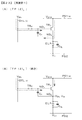
有機エレクトロルミネッセンス発光部(以下、単に、発光部と略称する場合がある)を駆動するための回路として、例えば、2つのトランジスタと1つの容量部から構成された駆動回路(2Tr/1C駆動回路と呼ぶ)が、特開2007−310311号公報(特許文献1)等から周知である。この2Tr/1C駆動回路は、図3に示すように、書込みトランジスタTRWと駆動トランジスタTRDの2つのトランジスタ、及び、1つの容量部C1から構成されている。 As a circuit for driving an organic electroluminescence light emitting unit (hereinafter, sometimes simply referred to as a light emitting unit), for example, a drive circuit (2Tr / 1C drive circuit configured with two transistors and one capacitor unit) Is known from JP 2007-310311 A (Patent Document 1) and the like. As shown in FIG. 3, the 2Tr / 1C drive circuit includes two transistors, a write transistor TR W and a drive transistor TR D , and a capacitor C 1 .
2Tr/1C駆動回路を備えた有機EL表示素子の動作の概要を説明する。図19にタイミングチャートを示すように、[期間−TP(2)3]及び[期間−TP(2)5]において、閾値電圧キャンセル処理が行われる。次いで、[期間−TP(2)7]において書込み処理が行われ、その後、[期間−TP(2)8]において、駆動トランジスタTRDのドレイン領域からソース領域へと流れるドレイン電流Idsが発光部ELPに流れる。基本的に、有機EL表示素子は、発光部ELPの発光効率と、発光部ELPに流れるドレイン電流Idsの値との積に応じた輝度で発光する。 An outline of the operation of the organic EL display element including the 2Tr / 1C driving circuit will be described. As shown in the timing chart of FIG. 19, the threshold voltage canceling process is performed in [Period-TP (2) 3 ] and [Period-TP (2) 5 ]. Next, a writing process is performed in [Period-TP (2) 7 ], and then, in [Period-TP (2) 8 ], the drain current I ds flowing from the drain region to the source region of the drive transistor TR D emits light. Flows to the part ELP. Basically, the organic EL display element emits light with a luminance corresponding to the product of the light emission efficiency of the light emitting unit ELP and the value of the drain current I ds flowing through the light emitting unit ELP.
尚、2Tr/1C駆動回路を備えた有機EL表示素子の動作については、後ほど、図19の他、後述する図20乃至図25を参照して、詳しく説明する。 The operation of the organic EL display element including the 2Tr / 1C driving circuit will be described in detail later with reference to FIGS. 20 to 25 described later in addition to FIG.
一般に、表示装置は、動作時間が長くなればなるほど輝度が低下する。有機EL表示素子を用いた表示装置においても、黒レベルを示す階調値の経時変化等により輝度の低下が観察される。従って、表示装置にあっては、同一のパターンを長時間表示させると、そのパターンに応じた輝度変化が観察されるといった所謂焼き付きが起こる場合がある。例えば、図28の(A)に示すように、有機EL表示装置の表示領域EAの右上に文字を表示(白表示)し、文字以外の領域を黒表示とした状態で、長時間表示装置を動作させる。その後、表示領域EA全体を白表示とすると、図28の(B)に示すように、表示領域EAにおいて、右上の文字表示をした部分の領域の輝度が相対的に低くなり、不要なパターンとして視認される。このように、焼き付きが起こると、表示装置の表示品質は低下する。 Generally, the brightness of the display device decreases as the operation time becomes longer. Even in a display device using an organic EL display element, a decrease in luminance is observed due to a change in gradation value indicating a black level with time. Therefore, in the display device, when the same pattern is displayed for a long time, a so-called burn-in in which a luminance change according to the pattern is observed may occur. For example, as shown in FIG. 28A, a character is displayed on the upper right of the display area EA of the organic EL display device (white display), and a region other than the characters is displayed in black, and the display device is operated for a long time. Make it work. Thereafter, when the entire display area EA is displayed in white, as shown in FIG. 28B, the luminance of the area where the upper right character is displayed in the display area EA is relatively low, and an unnecessary pattern is obtained. Visible. Thus, when image sticking occurs, the display quality of the display device deteriorates.
経時変化により黒レベルを示す階調値が大きくなる場合には、焼き付きを生じた領域の表示素子を駆動する際に、元の信号の階調値に黒レベルの階調値の変化量を加算して表示素子を制御するといったことによって、焼き付きを軽減することができる。しかしながら、例えば、有機EL表示素子を用いた表示装置において、黒レベルを示す階調値の経時変化は、表示する画像の輝度の履歴等によって左右される。動作履歴を種々変えたときの経時変化データを予め多数測定しておき、これらのデータを格納したテーブル等を参照して焼き付きを軽減するように制御するといった方法では、制御のための回路規模が大きくなると共に、制御が複雑になるといった問題が生ずる。 When the gradation value indicating the black level increases due to changes over time, the amount of change in the gradation value of the black level is added to the gradation value of the original signal when driving the display element in the area where the burn-in occurred. Then, the burn-in can be reduced by controlling the display element. However, for example, in a display device using an organic EL display element, a change in gradation value indicating a black level with time depends on a luminance history of an image to be displayed. In a method in which a large number of time-varying data when the operation history is changed is measured in advance and control is performed so as to reduce burn-in by referring to a table storing these data, the circuit scale for control is large. There is a problem that the control becomes complicated as the size increases.
従って、本発明の目的は、表示する画像の輝度の履歴等を個別にデータとして保存することなく、これらの履歴を反映して黒レベルを示す階調値の経時変化等に起因する焼き付きを軽減することができる表示装置を提供し、あるいは又、これらの履歴を反映して黒レベルを示す階調値の経時変化等に起因する焼き付きを軽減することができる表示装置の駆動方法を提供することにある。 Therefore, an object of the present invention is to save image brightness caused by a change in gradation value indicating a black level with time without reflecting the history of brightness of an image to be displayed as individual data. Provided is a display device that can be used, or a display device driving method that can reduce burn-in caused by a change in gradation value indicating a black level over time reflecting these histories. It is in.
上記の目的を達成するための本発明の表示装置は、
電流駆動型の発光部を有する表示素子が第1の方向と第2の方向とに2次元マトリクス状に配列されて成り、映像信号に基づいて画像を表示する表示パネル、及び、
入力信号の階調値を補正して映像信号として出力することによって、表示パネルが画像を表示する際の表示素子の輝度を補正する輝度補正部、
を備えており、
輝度補正部は、
表示素子が映像信号に基づいて所定の単位時間の間動作したときの表示素子の黒レベル階調値の経時変化と、表示素子が所定の基準階調値の映像信号に基づいて動作したと仮定したときの表示素子の黒レベル階調値の経時変化とが等しくなる基準動作時間の値を計算する基準動作時間値計算部、
基準動作時間値計算部が計算した基準動作時間の値を表示素子毎に累積した累積基準動作時間値を保持する累積基準動作時間値保持部、
表示素子が所定の基準階調値の映像信号に基づいて動作したときの、表示素子の動作時間と表示素子の黒レベル階調値の経時変化との関係を示す基準カーブを格納した基準カーブ格納部、
累積基準動作時間値保持部と基準カーブ格納部とを参照して表示素子の黒レベル階調値の経時変化を補償するための黒レベルシフト量を計算し、各表示素子に対応した黒レベルシフト量を保持する黒レベルシフト量保持部、及び、
黒レベルシフト量保持部に保持された黒レベルシフト量に基づいて、各表示素子に対応した入力信号の階調値を補正して映像信号として出力する映像信号生成部、
を備えている。
In order to achieve the above object, the display device of the present invention comprises:
A display panel having current-driven light emitting units arranged in a two-dimensional matrix in a first direction and a second direction, and displaying an image based on a video signal; and
A luminance correction unit that corrects the luminance of the display element when the display panel displays an image by correcting the gradation value of the input signal and outputting it as a video signal;
With
The brightness correction unit
Assumes that the display element has been operated based on a video signal having a predetermined reference gradation value and a change over time of the black level gradation value of the display element when the display element has been operated for a predetermined unit time based on the video signal. A reference operation time value calculation unit for calculating a reference operation time value at which the time-dependent change of the black level gradation value of the display element becomes equal,
An accumulated reference operation time value holding unit for holding an accumulated reference operation time value obtained by accumulating the reference operation time value calculated by the reference operation time value calculation unit for each display element;
Reference curve storage that stores a reference curve that indicates the relationship between the operating time of the display element and the time-dependent change in the black level gradation value of the display element when the display element operates based on a video signal having a predetermined reference gradation value Part,
The black level shift corresponding to each display element is calculated by referring to the accumulated reference operation time value holding unit and the reference curve storage unit to calculate the black level shift amount for compensating the change in the black level gradation value of the display element with time. A black level shift amount holding unit for holding the amount, and
A video signal generation unit that corrects the gradation value of the input signal corresponding to each display element and outputs it as a video signal based on the black level shift amount held in the black level shift amount holding unit,
It has.
また、上記の目的を達成するための本発明の表示装置の駆動方法は、
電流駆動型の発光部を有する表示素子が第1の方向と第2の方向とに2次元マトリクス状に配列されて成り、映像信号に基づいて画像を表示する表示パネル、及び、
入力信号の階調値を補正して映像信号として出力することによって、表示パネルが画像を表示する際の表示素子の輝度を補正する輝度補正部、
を備えた表示装置を用いた表示装置の駆動方法において、
輝度補正部の動作に基づいて、入力信号の階調値を補正して映像信号として出力することによって、表示パネルが画像を表示する際の表示素子の輝度を補正する輝度補正ステップを有し、
輝度補正ステップは、
表示素子が映像信号に基づいて所定の単位時間の間動作したときの黒レベル階調値の経時変化と、表示素子が所定の基準階調値の映像信号に基づいて動作したと仮定したときの表示素子の黒レベル階調値の経時変化とが等しくなる基準動作時間の値を計算する基準動作時間値計算ステップ、
基準動作時間の値を表示素子毎に累積した累積基準動作時間値を保持する累積基準動作時間値保持ステップ、
累積基準動作時間値と、表示素子が所定の基準階調値の映像信号に基づいて動作したときの表示素子の動作時間と表示素子の黒レベル階調値の経時変化との関係を示す基準カーブとを参照して表示素子の黒レベル階調値の経時変化を補償するための黒レベルシフト量を計算し、各表示素子に対応した黒レベルシフト量を保持する黒レベルシフト量保持ステップ、及び、
黒レベルシフト量に基づいて、各表示素子に対応した入力信号の階調値を補正して映像信号として出力する映像信号生成ステップ、
を備えている。
Further, a driving method of the display device of the present invention for achieving the above object is as follows.
A display panel having current-driven light emitting units arranged in a two-dimensional matrix in a first direction and a second direction, and displaying an image based on a video signal; and
A luminance correction unit that corrects the luminance of the display element when the display panel displays an image by correcting the gradation value of the input signal and outputting it as a video signal;
In a driving method of a display device using a display device comprising:
Based on the operation of the brightness correction unit, the brightness correction step of correcting the brightness of the display element when the display panel displays an image by correcting the gradation value of the input signal and outputting it as a video signal,
The brightness correction step
When the display element is operated for a predetermined unit time based on a video signal, the black level gradation value changes with time, and the display element is operated based on a video signal having a predetermined reference gradation value. A reference operation time value calculation step for calculating a reference operation time value at which the time-dependent change in the black level gradation value of the display element is equal;
An accumulated reference operation time value holding step for holding an accumulated reference operation time value obtained by accumulating a reference operation time value for each display element;
Reference curve showing the relationship between the accumulated reference operation time value and the change over time of the display element operation time and the display element black level gradation value when the display element operates based on a video signal having a predetermined reference gradation value And a black level shift amount holding step for calculating a black level shift amount for compensating a change with time of the black level gradation value of the display element, and holding a black level shift amount corresponding to each display element, and ,
A video signal generation step of correcting the gradation value of the input signal corresponding to each display element and outputting it as a video signal based on the black level shift amount,
It has.
本発明の表示装置によれば、表示する画像の輝度の履歴等を個別にデータとして保存することなく、これらの履歴を反映して黒レベルを示す階調値の経時変化等に起因する焼き付きを軽減することができる。また、本発明の表示装置の駆動方法によれば、表示する画像の輝度の履歴等を個別にデータとして保存することなく、これらの履歴を反映して黒レベルを示す階調値の経時変化等に起因する焼き付きを軽減するように制御することができる。 According to the display device of the present invention, the burn-in caused by the change over time in the gradation value indicating the black level reflecting these histories without separately storing the luminance histories of the displayed images as data. Can be reduced. Further, according to the driving method of the display device of the present invention, without changing the luminance history of the image to be displayed individually as data, the time-dependent change of the gradation value indicating the black level reflecting these history, etc. It is possible to control so as to reduce the burn-in caused by.
以下、図面を参照して、実施例に基づき本発明を説明するが、本発明は実施例に限定されるものではなく、実施例における種々の数値や材料は例示である。尚、説明は、以下の順序で行う。
1.本発明の表示装置及び表示装置の駆動方法、全般に関する説明
2.実施例1(表示装置及び表示装置の駆動方法)
Hereinafter, the present invention will be described based on examples with reference to the drawings. However, the present invention is not limited to the examples, and various numerical values and materials in the examples are examples. The description will be given in the following order.
1. 1. General description of display device and display device driving method of the present invention Example 1 (Display Device and Display Device Driving Method)
[本発明の表示装置及び表示装置の駆動方法、全般に関する説明]
本発明の表示装置及び表示装置の駆動方法において、入力信号及び映像信号の値は、デジタル制御を行うといった観点からは、2の冪乗で表される段階で値が変化するといった構成が好ましい。本発明の表示装置及び表示装置の駆動方法にあっては、焼き付きを軽減するために、映像信号の階調値が入力信号の階調値の最大値を超える値となる場合が生じ得る。
[Description of Display Device and Display Device Driving Method of the Present Invention, General]
In the display device and the driving method of the display device of the present invention, it is preferable that the values of the input signal and the video signal change at a stage represented by a power of 2 from the viewpoint of performing digital control. In the display device and the driving method of the display device of the present invention, in order to reduce burn-in, there may occur a case where the gradation value of the video signal exceeds the maximum value of the gradation value of the input signal.
例えば入力信号において8ビットの階調制御を行い、映像信号は8ビットを超える階調制御を行う構成とすることができる。一例として、映像信号を9ビット制御とするといった構成を挙げることができるが、これに限るものではない。 For example, 8-bit gradation control can be performed on the input signal, and gradation control exceeding 8 bits can be performed on the video signal. As an example, a configuration in which the video signal is controlled by 9 bits can be mentioned, but the configuration is not limited thereto.
本発明の表示装置、あるいは、本発明の表示装置の駆動方法に用いられる表示装置(以下、これらを総称して、単に、本発明の表示装置と呼ぶ場合がある)にあっては、
輝度補正部は、更に、
表示素子が各階調値の映像信号に基づいて動作するときの表示素子の黒レベル階調値の経時変化の速度と、表示素子が所定の基準階調値の映像信号に基づいて動作するときの表示素子の黒レベル階調値の経時変化の速度との比を動作時間換算係数テーブルとして格納した動作時間換算係数格納部、
を備えており、
基準動作時間値計算部は、
動作時間換算係数格納部の動作時間換算係数テーブルを参照し、映像信号の階調値に対応した動作時間換算係数の値を求め、単位時間の値に動作時間換算係数の値を乗算することによって、基準動作時間の値を計算する構成とすることができる。
In the display device of the present invention or the display device used in the driving method of the display device of the present invention (hereinafter, these may be collectively referred to simply as the display device of the present invention)
The brightness correction unit further
The rate of change over time of the black level gradation value of the display element when the display element operates based on the video signal of each gradation value, and the time when the display element operates based on the video signal of the predetermined reference gradation value An operation time conversion coefficient storage unit that stores a ratio of the black level gradation value of the display element with the rate of change over time as an operation time conversion coefficient table;
With
The reference operation time value calculator is
By referring to the operation time conversion coefficient table of the operation time conversion coefficient storage unit, obtaining the value of the operation time conversion coefficient corresponding to the gradation value of the video signal, and multiplying the unit time value by the value of the operation time conversion coefficient The reference operation time value can be calculated.
上述した好ましい構成の本発明の表示装置にあっては、
動作時間換算係数格納部には、表示素子の黒レベル階調値の経時変化の範囲毎に対応した複数の動作時間換算係数テーブルが格納されており、
基準動作時間値計算部は、黒レベルシフト量保持部に保持された黒レベルシフト量の値に対応した動作時間換算係数テーブルを選択して参照する構成とすることができる。
In the display device of the present invention having the preferred configuration described above,
The operation time conversion coefficient storage unit stores a plurality of operation time conversion coefficient tables corresponding to each time-dependent change range of the black level gradation value of the display element,
The reference operation time value calculation unit can be configured to select and refer to an operation time conversion coefficient table corresponding to the value of the black level shift amount held in the black level shift amount holding unit.
上述した各種の好ましい構成を含む本発明の表示装置にあっては、単位時間が短いほど、焼き付きの軽減の精度が向上するが、輝度補正部における処理の負担も増加する。単位時間は、表示装置の仕様に応じて適宜設定すればよい。 In the display device of the present invention including the various preferable configurations described above, the accuracy of reduction in burn-in improves as the unit time becomes shorter, but the processing burden on the luminance correction unit also increases. The unit time may be set as appropriate according to the specifications of the display device.
例えば、表示フレームレートの逆数で与えられる時間、換言すれば、所謂1フレーム期間が占める時間を単位時間とすることができる。あるいは又、所定の数のフレーム期間を纏めた期間が占める時間を単位時間とすることができる。尚、後者の構成にあっては、単位時間において、1つの表示素子に種々の階調値の映像信号が印加される。この場合には、例えば、単位時間の始期のフレーム期間における階調値のみ参照するといった構成とすればよい。 For example, the time given by the reciprocal of the display frame rate, in other words, the time occupied by so-called one frame period can be used as the unit time. Alternatively, the time occupied by a period of a predetermined number of frame periods can be set as a unit time. In the latter configuration, video signals having various gradation values are applied to one display element in a unit time. In this case, for example, only the gradation value in the first frame period of the unit time may be referred to.
輝度補正部を構成する、基準動作時間値計算部、累積基準動作時間値保持部、基準カーブ格納部、黒レベルシフト量保持部、映像信号生成部、及び、動作時間換算係数格納部は、周知の回路素子等を用いて構成することができる。後述する、電源部、走査回路、及び、信号出力回路等の各種の回路についても同様である。 The reference operation time value calculation unit, the accumulated reference operation time value holding unit, the reference curve storage unit, the black level shift amount holding unit, the video signal generation unit, and the operation time conversion coefficient storage unit that constitute the luminance correction unit are well known. These circuit elements can be used. The same applies to various circuits such as a power supply unit, a scanning circuit, and a signal output circuit described later.
上述した各種の好ましい構成を含む本発明の表示装置は、所謂モノクロ表示の構成であってもよいし、カラー表示の構成であってもよい。 The display device of the present invention including the various preferable configurations described above may have a so-called monochrome display configuration or a color display configuration.
カラー表示の構成とする場合には、1つの画素は複数の副画素から成る構成、具体的には、1つの画素は、赤色発光副画素、緑色発光副画素、及び、青色発光副画素の3つの副画素から成る構成とすることができる。更には、これらの3種の副画素に更に1種類あるいは複数種類の副画素を加えた1組(例えば、輝度向上のために白色光を発光する副画素を加えた1組、色再現範囲を拡大するために補色を発光する副画素を加えた1組、色再現範囲を拡大するためにイエローを発光する副画素を加えた1組、色再現範囲を拡大するためにイエロー及びシアンを発光する副画素を加えた1組)から構成することもできる。 In the case of a color display configuration, one pixel includes a plurality of sub-pixels. Specifically, one pixel includes three of a red light-emitting subpixel, a green light-emitting subpixel, and a blue light-emitting subpixel. A configuration including two sub-pixels can be adopted. Furthermore, a set of these three types of sub-pixels plus one or more types of sub-pixels (for example, a set of sub-pixels that emit white light to improve brightness, a color reproduction range) A set of sub-pixels that emit complementary colors for enlargement, a set of sub-pixels that emit yellow for expanding the color reproduction range, and yellow and cyan for expanding the color reproduction range It can also be composed of a set of subpixels).
表示装置の画素(ピクセル)の値として、VGA(640,480)、S−VGA(800,600)、XGA(1024,768)、APRC(1152,900)、S−XGA(1280,1024)、U−XGA(1600,1200)、HD−TV(1920,1080)、Q−XGA(2048,1536)の他、(1920,1035)、(720,480)、(1280,960)等、画像表示用解像度の幾つかを例示することができるが、これらの値に限定するものではない。 As values of pixels (pixels) of the display device, VGA (640, 480), S-VGA (800, 600), XGA (1024, 768), APRC (1152, 900), S-XGA (1280, 1024), U-XGA (1600, 1200), HD-TV (1920, 1080), Q-XGA (2048, 1536), (1920, 1035), (720, 480), (1280, 960), etc. Although some of the resolutions can be exemplified, the present invention is not limited to these values.
本発明の表示装置にあっては、表示素子を構成する電流駆動型の発光部として、有機エレクトロルミネッセンス発光部、LED発光部、半導体レーザ発光部等を挙げることができる。これらの発光部は、周知の材料や方法を用いて構成することができる。平面型の表示装置を構成する観点からは、中でも、発光部は、有機エレクトロルミネッセンス発光部から成る構成が好ましい。有機エレクトロルミネッセンス発光部は、いわゆる上面発光型であってもよいし、下面発光型であってもよい。有機エレクトロルミネッセンス発光部は、アノード電極、正孔輸送層、発光層、電子輸送層、カソード電極等から構成することができる。 In the display device of the present invention, an organic electroluminescence light emitting part, an LED light emitting part, a semiconductor laser light emitting part, and the like can be cited as current driven light emitting parts constituting the display element. These light emitting portions can be configured using known materials and methods. From the viewpoint of configuring a flat display device, it is preferable that the light emitting unit is composed of an organic electroluminescence light emitting unit. The organic electroluminescence light emitting unit may be a so-called top emission type or a bottom emission type. The organic electroluminescence light emitting part can be composed of an anode electrode, a hole transport layer, a light emitting layer, an electron transport layer, a cathode electrode, and the like.
表示パネルを構成する表示素子は、或る平面内に形成され(例えば、支持体上に形成され)ており、発光部は、例えば、層間絶縁層を介して、発光部を駆動する駆動回路の上方に形成されている。 The display element constituting the display panel is formed in a certain plane (for example, formed on a support), and the light emitting unit is a drive circuit that drives the light emitting unit via an interlayer insulating layer, for example. It is formed above.
発光部を駆動する駆動回路を構成するトランジスタとして、例えば、nチャネル型の薄膜トランジスタ(TFT)を挙げることができる。駆動回路を構成するトランジスタは、エンハンスメント型であってもよいし、デプレッション型であってもよい。nチャネル型のトランジスタにあってはLDD構造(Lightly Doped Drain構造)が形成されていてもよい。場合によっては、LDD構造は非対称に形成されていてもよい。例えば、駆動トランジスタに大きな電流が流れるのは表示素子の発光時であるので、発光時においてドレイン領域となる一方のソース/ドレイン領域にのみLDD構造を形成した構成とすることもできる。尚、例えば、pチャネル型の薄膜トランジスタを用いてもよい。 As an example of a transistor included in a driving circuit that drives the light emitting unit, an n-channel thin film transistor (TFT) can be given. The transistor constituting the driver circuit may be an enhancement type or a depletion type. In an n-channel transistor, an LDD structure (Lightly Doped Drain structure) may be formed. In some cases, the LDD structure may be formed asymmetrically. For example, since a large current flows through the driving transistor when the display element emits light, an LDD structure may be formed only in one of the source / drain regions that become the drain region during light emission. For example, a p-channel thin film transistor may be used.
駆動回路を構成する容量部は、一方の電極、他方の電極、及び、これらの電極に挟まれた誘電体層から構成することができる。駆動回路を構成する上述したトランジスタ及び容量部は、或る平面内に形成され(例えば、支持体上に形成され)、発光部は、例えば、層間絶縁層を介して、駆動回路を構成するトランジスタ及び容量部の上方に形成されている。また、駆動トランジスタの他方のソース/ドレイン領域は、発光部の一端(発光部に備えられたアノード電極等)に、例えば、コンタクトホールを介して接続されている。尚、半導体基板等にトランジスタを形成した構成であってもよい。 The capacitor portion constituting the drive circuit can be composed of one electrode, the other electrode, and a dielectric layer sandwiched between these electrodes. The above-described transistors and capacitors that constitute the drive circuit are formed in a certain plane (for example, formed on a support), and the light-emitting portion is a transistor that constitutes the drive circuit via an interlayer insulating layer, for example. And formed above the capacitor portion. In addition, the other source / drain region of the driving transistor is connected to one end of the light emitting unit (an anode electrode provided in the light emitting unit) via a contact hole, for example. In addition, the structure which formed the transistor in the semiconductor substrate etc. may be sufficient.
支持体や後述する基板の構成材料として、高歪点ガラス、ソーダガラス(Na2O・CaO・SiO2)、硼珪酸ガラス(Na2O・B2O3・SiO2)、フォルステライト(2MgO・SiO2)、鉛ガラス(Na2O・PbO・SiO2)等のガラス材料の他、可撓性を有する高分子材料、例えば、ポリエーテルスルホン(PES)やポリイミド、ポリカーボネート(PC)、ポリエチレンテレフタレート(PET)に例示される高分子材料を例示することができる。尚、支持体や基板の表面に各種のコーティングが施されていてもよい。支持体と基板の構成材料は、同じであってもよいし異なっていてもよい。可撓性を有する高分子材料から成る支持体及び基板を用いれば、可撓性を有する表示装置を構成することができる。 As a constituent material of a support or a substrate described later, high strain point glass, soda glass (Na 2 O · CaO · SiO 2 ), borosilicate glass (Na 2 O · B 2 O 3 · SiO 2 ), forsterite (2MgO・ In addition to glass materials such as SiO 2 ) and lead glass (Na 2 O · PbO · SiO 2 ), flexible polymer materials such as polyethersulfone (PES), polyimide, polycarbonate (PC), polyethylene A polymer material exemplified by terephthalate (PET) can be exemplified. Various coatings may be applied to the surface of the support or the substrate. The constituent materials of the support and the substrate may be the same or different. If a support body and a substrate made of a polymer material having flexibility are used, a display device having flexibility can be configured.
表示装置にあっては、走査線、データ線、給電線等の各種の配線は、周知の構成や構造とすることができる。 In the display device, various wirings such as a scanning line, a data line, and a power supply line can have a known configuration and structure.
1つのトランジスタの有する2つのソース/ドレイン領域において、「一方のソース/ドレイン領域」という用語を、電源側に接続されたソース/ドレイン領域といった意味において使用する場合がある。また、トランジスタが導通状態にあるとは、ソース/ドレイン領域間にチャネルが形成されている状態を意味する。係るトランジスタの一方のソース/ドレイン領域から他方のソース/ドレイン領域に電流が流れているか否かは問わない。一方、トランジスタが非導通状態にあるとは、ソース/ドレイン領域間にチャネルが形成されていない状態を意味する。また、ソース/ドレイン領域は、不純物を含有したポリシリコンやアモルファスシリコン等の導電性物質から構成することができるだけでなく、金属、合金、導電性粒子、これらの積層構造、有機材料(導電性高分子)から成る層から構成することができる。 In two source / drain regions of one transistor, the term “one source / drain region” may be used to mean a source / drain region connected to the power supply side. In addition, the transistor being in a conductive state means a state in which a channel is formed between the source / drain regions. It does not matter whether current flows from one source / drain region of the transistor to the other source / drain region. On the other hand, the transistor being in a non-conductive state means a state in which no channel is formed between the source / drain regions. In addition, the source / drain regions can be composed of conductive materials such as polysilicon or amorphous silicon containing impurities, as well as metals, alloys, conductive particles, their laminated structures, organic materials (conductivity high Molecule).
本明細書における各種の式に示す条件は、式が数学的に厳密に成立する場合の他、式が実質的に成立する場合にも満たされる。式の成立に関し、表示素子や表示装置の設計上あるいは製造上生ずる種々のばらつきの存在は許容される。 The conditions shown in the various expressions in this specification are satisfied not only when the expression is strictly mathematically established but also when the expression is substantially satisfied. Regarding the establishment of the expression, the existence of various variations that occur in the design or manufacture of the display element or the display device is allowed.
以下の説明で用いるタイミングチャートにおいて、各期間を示す横軸の長さ(時間長)は模式的なものであり、各期間の時間長の割合を示すものではない。縦軸においても同様である。また、タイミングチャートにおける波形の形状も模式的なものである。 In the timing chart used in the following description, the length of the horizontal axis (time length) indicating each period is a schematic one and does not indicate the ratio of the time length of each period. The same applies to the vertical axis. The waveform shape in the timing chart is also schematic.
実施例1は、本発明の表示装置及び表示装置の駆動方法に関する。 Example 1 relates to a display device and a driving method of the display device of the present invention.
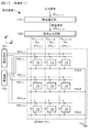
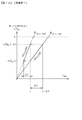
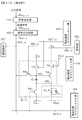
図1は、実施例1の表示装置1の概念図である。実施例1の表示装置1は、電流駆動型の発光部を有する表示素子10が第1の方向と第2の方向とに2次元マトリクス状に配列されて成り、映像信号VDSigに基づいて画像を表示する表示パネル20、及び、入力信号vDSigの階調値を補正して映像信号VDSigとして出力することによって、表示パネル20が画像を表示する際の表示素子10の輝度を補正する輝度補正部110を備えている。実施例1では、発光部は有機エレクトロルミネッセンス発光部から成る。
FIG. 1 is a conceptual diagram of a
表示素子10は、第1の方向(図1においてX方向、以下、行方向と呼ぶ場合がある)にN個、第2の方向(図1においてY方向、以下、列方向と呼ぶ場合がある)にM個、合計N×M個の、2次元マトリクス状に配列されている。表示素子10の行数はMであり、各行を構成する表示素子10の数はNである。尚、図1においては、3×3個の表示素子10を図示しているが、これは、あくまでも例示に過ぎない。
There are
表示パネル20は、更に、走査回路101に接続され、第1の方向に延びる複数(M本)の走査線SCL、信号出力回路102に接続され、第2の方向に延びる複数(N本)のデータ線DTL、及び、電源部100に接続され、第1の方向に延びる複数(M本)の給電線PS1を備えている。第m行目(但し、m=1,2・・・,M)の表示素子10は、第m番目の走査線SCLm、及び、第m番目の給電線PS1mに接続されており、1つの表示素子行を構成する。また、第n列目(但し、n=1,2・・・,N)の表示素子10は、第n番目のデータ線DTLnに接続されている。
The
電源部100及び走査回路101の構成や構造は、周知の構成や構造とすることができる。信号出力回路102は、図示せぬD/Aコンバータやラッチ回路を備えており、映像信号VDSigの階調値に基づいた映像信号電圧VSigを発生すると共に、一行分の映像信号電圧VSigを保持し、N本のデータ線DTLに映像信号電圧VSigを供給する。また、信号出力回路102は図示せぬセレクタ回路を備えており、セレクタ回路の切り替えによって、データ線DTLに映像信号電圧VSigを供給する状態と、データ線DTLに後述する基準電圧VOfsを供給する状態とが切り替えられる。電源部100、走査回路101、及び、信号出力回路102は、周知の回路素子等を用いて構成することができる。
The configurations and structures of the
実施例1の表示装置1は、複数の表示素子10(例えば、N×M=640×480)を備えている、モノクロ表示の表示装置である。各表示素子10は画素を構成する。表示領域においては、行方向と列方向とに2次元マトリクス状に画素が配列されている。
The
走査回路101からの走査信号によって、表示装置1は行単位で線順次走査される。第m行、第n列目に位置する表示素子10を、以下、第(n,m)番目の表示素子10あるいは第(n,m)番目の画素と呼ぶ。第(n,m)番目の表示素子10に対応する入力信号vDSigをvDSig(n,m)と表し、輝度補正部110により補正された第(n,m)番目の表示素子10に対応する映像信号VDSigを、VDSig(n,m)と表す。また、映像信号VDSig(n,m)に基づいた映像信号電圧をVSig(n,m)と表す。
With the scanning signal from the
上述したように、輝度補正部110は、入力信号vDSigの階調値を補正して映像信号VDSigとして出力する。
As described above, the
説明の都合上、入力信号vDSigの階調ビット数は8ビットであるとする。入力信号vDSigの階調値は、表示すべき画像の輝度に応じて、0乃至255のいずれかの値となる。ここでは、階調値が大きいほど表示すべき画像の輝度が高いものとする。また、説明の都合上、映像信号VDSigの階調ビット数は9ビットであるとする。 For convenience of explanation, it is assumed that the number of gradation bits of the input signal vD Sig is 8 bits. The gradation value of the input signal vD Sig is any value from 0 to 255 depending on the luminance of the image to be displayed. Here, it is assumed that the luminance of the image to be displayed increases as the gradation value increases. For convenience of explanation, it is assumed that the number of gradation bits of the video signal VD Sig is 9 bits.
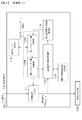
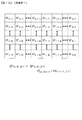
図2は、輝度補正部110の構成を説明するための、模式的なブロック図である。輝度補正部110の動作については、後ほど、後述する図14乃至図18を参照して詳しく説明する。ここでは、輝度補正部110の概要について説明する。
FIG. 2 is a schematic block diagram for explaining the configuration of the
輝度補正部110は、基準動作時間値計算部112、累積基準動作時間値保持部114、基準カーブ格納部116、黒レベルシフト量保持部115、及び、映像信号生成部111を備えており、更に、動作時間換算係数格納部113を備えている。これらは、演算回路や記憶装置(メモリ)等から構成されており、周知の回路素子等を用いて構成することができる。
The
基準動作時間値計算部112は、表示素子10が映像信号VDSigに基づいて所定の単位時間の間動作したときの表示素子10の黒レベル階調値の経時変化と、表示素子10が所定の基準階調値の映像信号VDSigに基づいて動作したと仮定したときの表示素子10の黒レベル階調値の経時変化とが等しくなる基準動作時間の値を計算する。「所定の単位時間」及び「所定の基準階調値」については、後述する。
The reference operation time
動作時間換算係数格納部113には、表示素子10が各階調値の映像信号VDSigに基づいて動作するときの表示素子10の黒レベル階調値の経時変化の速度と、表示素子10が所定の基準階調値の映像信号VDSigに基づいて動作するときの表示素子10の黒レベル階調値の経時変化の速度との比が動作時間換算係数テーブルとして格納されている。
In the operation time conversion
より具体的には、動作時間換算係数格納部113には、表示素子10の黒レベル階調値の経時変化の範囲毎に対応した複数の動作時間換算係数テーブルが格納されている。実施例1では、動作時間換算係数格納部113には、図14のグラフに示す関係を表す関数fCSC_BS1,fCSC_BS2,fCSC_BS3,fCSC_BS4がテーブルとして予め格納されている。
More specifically, the operation time conversion
動作時間換算係数格納部113は、所謂不揮発性メモリといった記憶装置から構成することができる。後述する基準カーブ格納部116においても同様である。
The operation time conversion
基準動作時間値計算部112は、動作時間換算係数格納部113の動作時間換算係数テーブルを参照し、映像信号VDSigの階調値に対応した動作時間換算係数の値を求め、単位時間の値に動作時間換算係数の値を乗算することによって、基準動作時間の値を計算する。より具体的には、基準動作時間値計算部112は、黒レベルシフト量保持部115に保持された黒レベルシフト量の値に対応した動作時間換算係数テーブルを選択して参照する。
The reference operation time
累積基準動作時間値保持部114は、基準動作時間値計算部112が計算した基準動作時間の値を表示素子10毎に累積した累積基準動作時間値を保持する。累積基準動作時間値は、表示装置1の動作履歴を反映した値であり、表示装置1の電源遮断等によってリセットされない。累積基準動作時間値保持部114は、各表示素子10に対応した記憶領域を持つ書き換え可能な不揮発性の記憶装置から構成されており、図15に示すデータを保持する。
The accumulated reference operation time
基準カーブ格納部116には、表示素子10が所定の基準階調値の映像信号VDSigに基づいて動作したときの、表示素子10の動作時間と表示素子10の黒レベル階調値の経時変化との関係を示す基準カーブが格納されている。具体的には、基準カーブ格納部116には、図16に示す基準カーブを表す関数fREF_BS_SHIFTがテーブルとして予め格納されている。
In the reference
尚、上述した関数fCSC_BS1,fCSC_BS2,fCSC_BS3,fCSC_BS4、関数fREF_BS_SHIFTは、同一仕様の表示装置を用いた実測等によるデータに基づき予め決定されている。 The functions f CSC_BS1 , f CSC_BS2 , f CSC_BS3 , f CSC_BS4 , and function f REF_BS_SHIFT described above are determined in advance based on data obtained by actual measurement using a display device having the same specifications.
実施例1にあっては、「所定の単位時間」を所謂1フレーム期間が占める時間とし、「所定の基準階調値」を500としたが、これに限定するものではない。 In the first embodiment, the “predetermined unit time” is the time occupied by a so-called one frame period, and the “predetermined reference gradation value” is 500. However, the present invention is not limited to this.
黒レベルシフト量保持部115は、累積基準動作時間値保持部114と基準カーブ格納部116とを参照して表示素子10の黒レベル階調値の経時変化を補償するための黒レベルシフト量を計算し、各表示素子10に対応した黒レベルシフト量を保持する。
The black level shift amount holding unit 115 refers to the accumulated reference operation time
黒レベルシフト量保持部115は、黒レベルシフト量計算部115Aと黒レベルシフト量格納部115Bとから構成されている。黒レベルシフト量計算部115Aは演算回路から構成されている。黒レベルシフト量格納部115Bは、各表示素子10に対応した記憶領域を持ち、書き換え可能な不揮発性の記憶装置から構成されており、図18に示すデータを保持する。図18に示すデータは、表示装置1の電源遮断等によってリセットされない。
The black level shift amount holding unit 115 includes a black level shift
映像信号生成部111は、黒レベルシフト量保持部115に保持された黒レベルシフト量に基づいて、各表示素子10に対応した入力信号vDSigの階調値を補正して映像信号VDSigとして出力する。
The video
以上、輝度補正部110の概要を説明した。次いで、表示装置1の構成について説明する。
The outline of the
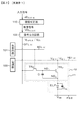
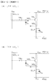
図3は、表示パネル20を構成する表示素子10の等価回路図である。
FIG. 3 is an equivalent circuit diagram of the
表示素子10は、電流駆動型の発光部ELPと駆動回路11を含んでいる。駆動回路11は、ゲート電極とソース/ドレイン領域とを有する駆動トランジスタTRD、及び、容量部C1を少なくとも備えており、駆動トランジスタTRDのソース/ドレイン領域を介して発光部ELPに電流が流れる。後で図4を参照して詳しく説明するが、表示素子10は、駆動回路11と、この駆動回路11に接続された発光部ELPとが積層された構造を有する。
The
駆動回路11は、駆動トランジスタTRDに加えて、更に、書込みトランジスタTRWを備えている。駆動トランジスタTRDと書込みトランジスタTRWは、nチャネル型のTFTから成る。尚、例えば書込みトランジスタTRWがpチャネル型のTFTから成る構成とすることもできる。また、駆動回路11は、例えば後述する図26や図27に示すように、更に別のトランジスタを備えていてもよい。
Drive
容量部C1は、駆動トランジスタTRDのソース領域に対するゲート電極の電圧(所謂ゲート−ソース間電圧)を保持するために用いられる。この場合の「ソース領域」とは、発光部ELPが発光するときに「ソース領域」として働く側のソース/ドレイン領域を意味する。表示素子10の発光状態においては、駆動トランジスタTRDの一方のソース/ドレイン領域(図3において給電線PS1に接続されている側)はドレイン領域として働き、他方のソース/ドレイン領域(発光部ELPの一端、具体的には、アノード電極に接続されている側)はソース領域として働く。容量部C1を構成する一方の電極と他方の電極は、それぞれ、駆動トランジスタTRDの他方のソース/ドレイン領域とゲート電極に接続されている。
The capacitor unit C 1 is used to hold the voltage of the gate electrode with respect to the source region of the driving transistor TR D (so-called gate-source voltage). The “source region” in this case means a source / drain region on the side that functions as a “source region” when the light emitting unit ELP emits light. In the light emitting state of the
書込みトランジスタTRWは、走査線SCLに接続されたゲート電極と、データ線DTLに接続された一方のソース/ドレイン領域と、駆動トランジスタTRDのゲート電極に接続された他方のソース/ドレイン領域とを有する。 The write transistor TR W includes a gate electrode connected to the scanning line SCL, one source / drain region connected to the data line DTL, and the other source / drain region connected to the gate electrode of the drive transistor TR D. Have
駆動トランジスタTRDのゲート電極は、書込みトランジスタTRWの他方のソース/ドレイン領域と容量部C1の他方の電極とが接続された、第1ノードND1を構成する。駆動トランジスタTRDの他方のソース/ドレイン領域は、容量部C1の一方の電極と発光部ELPのアノード電極とが接続された、第2ノードND2を構成する。 The gate electrode of the drive transistor TR D forms a first node ND 1 in which the other source / drain region of the write transistor TR W and the other electrode of the capacitor C 1 are connected. The other source / drain region of the driving transistor TR D forms a second node ND 2 in which one electrode of the capacitor C 1 and the anode electrode of the light emitting unit ELP are connected.
発光部ELPの他端(具体的には、カソード電極)は、第2の給電線PS2に接続されている。尚、図1に示すように、第2の給電線PS2は、全ての表示素子10において共通である。
The other end of the light emitting unit ELP (specifically, the cathode electrode) is connected to the second power supply line PS2. As shown in FIG. 1, the second power supply line PS <b> 2 is common to all the
発光部ELPのカソード電極には、第2の給電線PS2から、後述する所定の電圧VCatが印加される。発光部ELPの容量を符号CELで表す。また、発光部ELPの発光に必要とされる閾値電圧をVth-ELとする。即ち、発光部ELPのアノード電極とカソード電極との間にVth-EL以上の電圧が印加されると、発光部ELPは発光する。 A predetermined voltage V Cat described later is applied from the second feeder line PS2 to the cathode electrode of the light emitting unit ELP. The capacity of the light emitting part ELP is represented by the symbol C EL . Further, the threshold voltage required for light emission of the light emitting unit ELP is set to V th-EL . That is, when a voltage equal to or higher than V th-EL is applied between the anode electrode and the cathode electrode of the light emitting unit ELP, the light emitting unit ELP emits light.
発光部ELPは、例えば、アノード電極、正孔輸送層、発光層、電子輸送層、及び、カソード電極等から成る周知の構成や構造を有する。 The light emitting unit ELP has a known configuration and structure including, for example, an anode electrode, a hole transport layer, a light emitting layer, an electron transport layer, and a cathode electrode.
図3に示す駆動トランジスタTRDは、表示素子10の発光状態においては、飽和領域で動作するように電圧設定されており、以下の式(1)に従ってドレイン電流Idsを流すように駆動される。上述したように、表示素子10の発光状態においては、駆動トランジスタTRDの一方のソース/ドレイン領域はドレイン領域として働き、他方のソース/ドレイン領域はソース領域として働く。説明の都合上、以下、駆動トランジスタTRDの一方のソース/ドレイン領域を単にドレイン領域と呼び、他方のソース/ドレイン領域を単にソース領域と呼ぶ場合がある。尚、
μ :実効的な移動度
L :チャネル長
W :チャネル幅
Vgs:ソース領域に対するゲート電極の電圧
Vth:閾値電圧
Cox:(ゲート絶縁層の比誘電率)×(真空の誘電率)/(ゲート絶縁層の厚さ)
k≡(1/2)・(W/L)・Cox
とする。
The driving transistor TR D shown in FIG. 3 is set to a voltage so as to operate in the saturation region in the light emitting state of the
μ: Effective mobility L: Channel length W: Channel width V gs : Voltage of gate electrode with respect to source region V th : Threshold voltage C ox : (Relative permittivity of gate insulating layer) × (dielectric constant of vacuum) / (Gate insulation layer thickness)
k≡ (1/2) ・ (W / L) ・ C ox
And
Ids=k・μ・(Vgs−Vth)2 (1) I ds = k · μ · (V gs −V th ) 2 (1)
このドレイン電流Idsが発光部ELPを流れることで、表示素子10の発光部ELPが発光する。更には、このドレイン電流Idsの値の大小によって、表示素子10の発光部ELPにおける発光状態(輝度)が制御される。
When the drain current I ds flows through the light emitting unit ELP, the light emitting unit ELP of the
書込みトランジスタTRWの導通状態/非導通状態は、書込みトランジスタTRWのゲート電極に接続された走査線SCLからの走査信号、具体的には、走査回路101からの走査信号によって制御される。
Conductive state / nonconductive state of the writing transistor TR W, the scanning signal from the scanning line connected SCL to a gate electrode of the writing transistor TR W, specifically, are controlled by a scanning signal from the
書込みトランジスタTRWの一方のソース/ドレイン領域には、データ線DTLから、信号出力回路102の動作に基づいて種々の信号や電圧が印加される。具体的には、信号出力回路102から、映像信号電圧VSigと所定の基準電圧VOfsが印加される。尚、映像信号電圧VSigや基準電圧VOfsに加えて更に別の電圧が印加されるといった構成であってもよい。
Various signals and voltages are applied to one source / drain region of the write transistor TR W from the data line DTL based on the operation of the
走査回路101からの走査信号によって、表示装置1は行単位で線順次走査される。各水平走査期間にあっては、データ線DTLには先ず基準電圧VOfsが印加され、その後、映像信号電圧VSigが供給される。
With the scanning signal from the
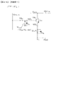
図4に表示装置1を構成する表示パネル20の一部分の模式的な一部断面図を示す。駆動回路11を構成するトランジスタTRD,TRW及び容量部C1は支持体21上に形成され、発光部ELPは、例えば、層間絶縁層40を介して、駆動回路11を構成するトランジスタTRD,TRW及び容量部C1の上方に形成されている。また、駆動トランジスタTRDの他方のソース/ドレイン領域は、発光部ELPに備えられたアノード電極に、コンタクトホールを介して接続されている。尚、図4においては、駆動トランジスタTRDのみを図示する。その他のトランジスタは隠れて見えない。
FIG. 4 shows a schematic partial sectional view of a part of the
より具体的には、駆動トランジスタTRDは、ゲート電極31、ゲート絶縁層32、半導体層33に設けられたソース/ドレイン領域35,35、及び、ソース/ドレイン領域35,35の間の半導体層33の部分が該当するチャネル形成領域34から構成されている。一方、容量部C1は、他方の電極36、ゲート絶縁層32の延在部から構成された誘電体層、及び、一方の電極37から成る。ゲート電極31、ゲート絶縁層32の一部、及び、容量部C1を構成する他方の電極36は、支持体21上に形成されている。駆動トランジスタTRDの一方のソース/ドレイン領域35は配線38(給電線PS1に対応する)に接続され、他方のソース/ドレイン領域35は一方の電極37に接続されている。駆動トランジスタTRD及び容量部C1等は、層間絶縁層40で覆われており、層間絶縁層40上に、アノード電極51、正孔輸送層、発光層、電子輸送層、及び、カソード電極53から成る発光部ELPが設けられている。尚、図面においては、正孔輸送層、発光層、及び、電子輸送層を1層52で表した。発光部ELPが設けられていない層間絶縁層40の部分の上には、第2層間絶縁層54が設けられ、第2層間絶縁層54及びカソード電極53上には透明な基板22が配置されており、発光層にて発光した光は、基板22を通過して、外部に出射される。尚、一方の電極37とアノード電極51とは、層間絶縁層40に設けられたコンタクトホールによって接続されている。また、カソード電極53は、第2層間絶縁層54、層間絶縁層40に設けられたコンタクトホール56,55を介して、ゲート絶縁層32の延在部上に設けられた配線39(第2の給電線PS2に対応する)に接続されている。
More specifically, the drive transistor TR D includes a
図4に示す表示パネル20を備えた表示装置1の製造方法を説明する。先ず、支持体21上に、走査線SCL等の各種配線、容量部C1を構成する電極、半導体層から成るトランジスタ、層間絶縁層、コンタクトホール等を、周知の方法により適宜形成する。次いで、周知の方法により成膜及びパターニングを行い、マトリクス状に配列された発光部ELPを形成する。そして、上記工程を経た支持体21と基板22を対向させ周囲を封止した後、外部の回路との結線を行い、表示装置を得ることができる。
A method for manufacturing the
次いで、実施例1の表示装置1の駆動方法(以下、単に、実施例1の駆動方法と略称する場合がある)について説明する。表示装置1の表示フレームレートをFR(回/秒)とする。第m行目に配列されたN個の画素のそれぞれを構成する表示素子10が同時に駆動される。換言すれば、第1の方向に沿って配されたN個の表示素子10にあっては、その発光/非発光のタイミングは、それらが属する行単位で制御される。表示装置1を行単位で線順次走査するときの1行当たりの走査期間、より具体的には、1水平走査期間(所謂1H)は、(1/FR)×(1/M)秒未満である。
Next, a driving method of the
以下の説明において、電圧あるいは電位の値を以下のとおりとするが、これは、あくまでも説明のための値であり、これらの値に限定されるものではない。 In the following description, the voltage or potential value is as follows. However, this is merely a value for explanation, and is not limited to these values.
VSig :映像信号電圧
・・・0ボルト(階調値0)〜10ボルト(階調値511)
VOfs :駆動トランジスタTRDのゲート電極(第1ノードND1)に印加する基準電圧
・・・0ボルト
VCC-H :発光部ELPに電流を流すための駆動電圧
・・・20ボルト
VCC-L :駆動トランジスタTRDの他方のソース/ドレイン領域(第2ノードND2)の
電位を初期化するための初期化電圧
・・・−10ボルト
Vth :駆動トランジスタTRDの閾値電圧
・・・3ボルト
VCat :発光部ELPのカソード電極に印加される電圧
・・・0ボルト
Vth-EL:発光部ELPの設計上の閾値電圧
・・・4ボルト
V Sig : Video signal voltage: 0 volts (gradation value 0) to 10 volts (gradation value 511)
V Ofs: driving transistor TR D reference voltage. 0 volts applied to the gate electrode (first node ND 1) of the V CC-H: drive for supplying a current to the light emitting section ELP voltage ... 20 volts V CC -L: driving transistor TR D other source / drain region (second node ND 2) initializing voltage ... -10 volts V th for initializing the potential of: threshold voltage · the drive transistor TR D・ 3 volts V Cat : voltage applied to the cathode electrode of the light emitting part ELP... 0 volt V th-EL : threshold voltage in design of the light emitting part ELP.
第(n,m)番目の表示素子10の動作については、後ほど、図19乃至図25を参照して詳しく説明する。先ず、映像信号VDSigと映像信号電圧VSigの関係について説明する。
The operation of the (n, m)
背景技術の欄においても説明したが、図19にタイミングチャートを示すように、[期間−TP(2)3]及び[期間−TP(2)5]において、閾値電圧キャンセル処理が行われる。次いで、[期間−TP(2)7]において書込み処理が行われ、その後、[期間−TP(2)8]において、駆動トランジスタTRDのドレイン領域からソース領域へと流れるドレイン電流Idsが発光部ELPに流れ、発光部ELPが発光する。 As described in the background art section, as shown in the timing chart of FIG. 19, the threshold voltage canceling process is performed in [Period-TP (2) 3 ] and [Period-TP (2) 5 ]. Next, a writing process is performed in [Period-TP (2) 7 ], and then, in [Period-TP (2) 8 ], the drain current I ds flowing from the drain region to the source region of the drive transistor TR D emits light. The light emitting part ELP emits light.
図19及び図24の(B)に示すように、[期間−TP(2)7]の終期において、第2ノードND2の電位は(VOfs−Vth+ΔV)である。そして、駆動トランジスタTRDのソース領域に対するゲート電極の電圧Vgsは、以下の式(4)のように表すことができる。 As shown in FIGS. 19 and 24B, at the end of [Period-TP (2) 7 ], the potential of the second node ND 2 is (V Ofs −V th + ΔV). The voltage V gs of the gate electrode with respect to the source region of the drive transistor TR D can be expressed as in the following formula (4).
Vgs≒VSig_m−(VOfs−Vth)−ΔV (4) V gs ≈V Sig — m − (V Ofs −V th ) −ΔV (4)
式(4)において、「VSig_m」は第(n,m)番目の表示素子10の映像信号電圧VSig(n,m)を示しており、「ΔV」は、第2ノードND2の電位の上昇量ΔV(電位補正値)である。電位補正値ΔVについては、後ほど、図24の(B)を参照して詳しく説明する。
In Expression (4), “V Sig_m ” indicates the video signal voltage V Sig (n, m) of the (n, m)
図19及び図25に示すように、[期間−TP(2)8]において駆動トランジスタTRDのソース領域の電位は上昇する。また、所謂ブートストラップ回路におけると同様の動作(ブートストラップ動作)が生じ、駆動トランジスタTRDのゲート電極の電位も上昇する。 As shown in FIG. 19 and FIG. 25, the potential of the source region of the drive transistor TR D rises in [Period -TP (2) 8 ]. Also, creating similar operation (bootstrap operation) as in so-called bootstrap circuit, also increases the potential of the gate electrode of the driving transistor TR D.
即ち、[期間−TP(2)8]にあっては、第1ノードND1は浮遊状態となり、第2ノードND2の電位は、(VOfs−Vth+ΔV)から、発光部ELPの閾値電圧Vth-ELを超える電位まで上昇する。ブートストラップ動作が理想的に起こる場合、換言すれば、第1ノードND1の電位の上昇量が第2ノードND2の電位の上昇量と等しくなるといった場合には、[期間−TP(2)8]においても、電圧Vgsは上述した式(4)で与えられる値を維持する。第(n,m)番目の表示素子10の発光部ELPに流れドレイン電流Idsは、上述した式(1)と式(4)から、以下の式(5)のように表すことができる。
That is, in [Period -TP (2) 8 ], the first node ND 1 is in a floating state, and the potential of the second node ND 2 is changed from (V Ofs −V th + ΔV) to the threshold value of the light emitting unit ELP. It rises to a potential exceeding the voltage V th-EL . When the bootstrap operation occurs ideally, in other words, when the amount of increase in the potential of the first node ND 1 becomes equal to the amount of increase in the potential of the second node ND 2 , [period-TP (2) 8 ], the voltage V gs maintains the value given by the above-described equation (4). The drain current I ds flowing in the light emitting part ELP of the (n, m)
Ids=k・μ・(VSig_m−VOfs−ΔV)2 (5) I ds = k · μ · (V Sig — m −V Ofs −ΔV) 2 (5)
説明の都合上、ここでは、「ΔV」の値はVSig_mに比べて充分小さいとする。上述したように、VOfsは0ボルトであるので、式(5)は、式(5’)のように変形することができる。 For convenience of explanation, it is assumed here that the value of “ΔV” is sufficiently smaller than V Sig — m . As described above, since V Ofs is 0 volt, equation (5) can be transformed into equation (5 ′).
Ids=k・μ・VSig_m 2 (5’) I ds = k · μ · V Sig_m 2 (5 ′)
式(5’)から明らかなように、ドレイン電流Idsは、映像信号電圧VSig(n,m)の値の自乗に比例する。表示素子10は、発光部ELPの発光効率と、発光部ELPに流れるドレイン電流Idsの値との積に応じた輝度で発光する。従って、映像信号電圧VSigの値は、基本的には、映像信号VDSigの階調値の平方根に比例するように設定されている。
As apparent from the equation (5 ′), the drain current I ds is proportional to the square of the value of the video signal voltage V Sig (n, m) . The
図5の(A)は、初期状態の表示素子10における映像信号電圧VSigの値と表示素子10の輝度の値LUとの関係を説明するためのグラフである。
FIG. 5A is a graph for explaining the relationship between the value of the video signal voltage V Sig in the
図5の(A)の横軸は、映像信号電圧VSigの値である。尚、横軸には、対応する映像信号VDSigの階調値を[]で囲んで記載した。後述する図5(B)においても同様である。また、他の図面においても、[]で囲んだ数値は階調値を表す。 In FIG. 5A, the horizontal axis represents the value of the video signal voltage V Sig . On the horizontal axis, the gradation value of the corresponding video signal VD Sig is shown enclosed in []. The same applies to FIG. 5B described later. Also in other drawings, the numerical value enclosed in [] represents the gradation value.
上述した係数「k」と係数「μ」と発光部ELPの初期状態の発光効率等とによって定まる係数をαIniと表せば、輝度LUは、
LU=(VDSig−ΔD)×αIni
といった式で表すことができる。ここで、「ΔD」は、所謂黒レベルの階調であり、表示装置1の仕様や設計によって定まる。尚、VDSig<ΔDの場合には、式においてLUの値が負となるが、この場合にはLUは「0」として扱う。
If the coefficient determined by the coefficient “k”, the coefficient “μ”, and the light emission efficiency of the light emitting unit ELP in the initial state is expressed as α Ini , the luminance LU is
LU = (VD Sig −ΔD) × α Ini
It can be expressed by the following formula. Here, “ΔD” is a so-called black level gradation and is determined by the specifications and design of the
説明の都合上、ここでは、ΔDの値は0であるとする。この場合には、
LU=VDSig×αIni
と表すことができる。例えば、αIni=1.2であるとすれば、初期状態の表示装置1において階調値500の映像信号VDSigに基づいて画像を表示する場合、画像の輝度は概ね600cd/m2となる。尚、実施例1にあっては、表示装置1の仕様上の輝度の最大値は、255×αIniである。
For convenience of explanation, it is assumed here that the value of ΔD is zero. In this case,
LU = VD Sig × α Ini
It can be expressed as. For example, when α Ini = 1.2, when an image is displayed on the
次いで、表示素子10の黒レベルを示す階調値の経時変化と、それに起因する焼き付きを軽減する方法の原理について説明する。
Next, the principle of the method for reducing the temporal change of the gradation value indicating the black level of the
一般に、表示素子10を構成する発光部ELPやトランジスタTRD,TRWの特性は、表示装置1の使用履歴に応じて経時変化を示す。例えば、発光部ELPの閾値電圧Vth-ELの値は、表示素子10の動作時間や動作時の映像信号VDSigの階調値によって影響を受け、定性的には徐々にその値が大きくなるといった経時変化を示す。
In general, the characteristics of the light emitting unit ELP and the transistors TR D and TR W constituting the
ブートストラップ動作が理想的に起こるのであれば、発光部ELPの閾値電圧Vth-ELの経時変化が、ドレイン電流Idsの値に影響を与えるといったことはない。しかしながら、実際には、駆動トランジスタTRDの寄生容量等の影響により、ブートストラップ動作における第1ノードND1の電位の上昇量は、第2ノードND2の電位の上昇量よりも小さくなる。換言すれば、ブートストラップ動作時の第2ノードND2の電位の上昇量が大きくなるほど、駆動トランジスタTRDのソース領域に対するゲート電極の電圧Vgsの値は小さくなる。 If the bootstrap operation occurs ideally, the change over time of the threshold voltage V th-EL of the light emitting unit ELP does not affect the value of the drain current I ds . However, in actuality, the amount of increase in the potential of the first node ND 1 in the bootstrap operation is smaller than the amount of increase in the potential of the second node ND 2 due to the influence of the parasitic capacitance and the like of the drive transistor TR D. In other words, the value of the gate electrode voltage V gs with respect to the source region of the driving transistor TR D decreases as the amount of increase in the potential of the second node ND 2 during the bootstrap operation increases.
そして、上述したように、[期間−TP(2)8]にあっては、第2ノードND2の電位は発光部ELPの閾値電圧Vth-ELを超える電位まで上昇する。従って、発光部ELPの閾値電圧Vth-ELの値が経時変化により大きくなるほど、[期間−TP(2)8]における第2ノードND2の電位の上昇量は大きくなり、駆動トランジスタTRDのソース領域に対するゲート電極の電圧Vgsの値は小さくなる。閾値電圧Vth-ELの経時変化に起因する電圧Vgsの変化量を符号ΔVBSで表せば、[期間−TP(2)8]における電圧Vgsは、以下の式(4’)のように表すことができる。 As described above, in [Period -TP (2) 8 ], the potential of the second node ND 2 rises to a potential exceeding the threshold voltage V th-EL of the light emitting unit ELP. Therefore, as the value of the threshold voltage V th-EL of the light emitting unit ELP increases with time, the amount of increase in the potential of the second node ND 2 in [period-TP (2) 8 ] increases, and the drive transistor TR D The value of the gate electrode voltage V gs with respect to the source region becomes small. Expressed the variation of the voltage V gs due to aging of the threshold voltage V th-EL by symbol [Delta] V BS, the voltage V gs at [Period -TP (2) 8] is shown in the following formula (4 ') Can be expressed as
Vgs≒VSig_m−(VOfs−Vth)−ΔV−ΔVBS (4’) V gs ≈V Sig — m − (V Ofs −V th ) −ΔV−ΔV BS (4 ′)
従って、この場合には、式(5’)は、以下の式(5”)のように変形することができる。 Therefore, in this case, the equation (5 ′) can be transformed into the following equation (5 ″).
Ids=k・μ・(VSig_m−ΔVBS)2 (5”) I ds = k · μ · (V Sig — m −ΔV BS ) 2 (5 ″)
図5の(B)は、経時変化を生じた表示素子10における映像信号電圧VSigの値と表示素子10の輝度の値との関係を説明するためのグラフである。
FIG. 5B is a graph for explaining the relationship between the value of the video signal voltage V Sig and the luminance value of the
図5の(B)に示すように、経時変化後の特性カーブは、初期特性の特性カーブを、横方向に電圧ΔVBSシフトしたカーブとなる。この特性カーブから明らかなように、黒レベルを示す映像信号電圧VSigの値は、ΔVBSの値だけシフトする。電圧ΔVBSに対応する階調値を符号ΔVDBSで表せば、表示素子10の黒レベルを示す階調値は、ΔVDBSシフトする。即ち、ΔVDBSは黒レベル経時変化量である。
As shown in FIG. 5B, the characteristic curve after change with time is a curve obtained by shifting the characteristic curve of the initial characteristic by a voltage ΔV BS in the horizontal direction. As is apparent from this characteristic curve, the value of the video signal voltage V Sig indicating the black level is shifted by the value of ΔV BS . If the gradation value corresponding to the voltage ΔV BS is represented by the sign ΔVD BS , the gradation value indicating the black level of the
従って、表示素子10の黒レベルを示す階調値の経時変化に起因する焼き付きを軽減するには、基本的には、映像信号VDSigの階調値に、上述したΔVDBSに相当する値の黒レベルシフト量を加算して、表示素子10を動作させればよい。
Therefore, to reduce image sticking caused by aging of the gradation value indicating the black level of the
以上、表示素子10の黒レベルを示す階調値の経時変化に起因する焼き付きを軽減する方法の原理について説明した。表示素子10の黒レベルを示す階調値の経時変化は、表示装置1に表示する画像の輝度及び動作時間の履歴によっても左右される。表示素子10の黒レベルを示す階調値の経時変化の程度は、表示素子10毎に異なる。従って、表示装置1の焼き付きを軽減するためには、表示素子10毎に映像信号VDSigの階調値を制御するといったことが必要になる。
The principle of the method for reducing the burn-in caused by the change over time in the gradation value indicating the black level of the
図2を参照して、表示装置1における焼き付きを軽減する方法の概略を説明する。各表示素子10に対応した黒レベルシフト量を、累積基準動作時間値保持部114に保持されたデータに基づいて基準カーブ格納部116を参照して計算する。そして、その黒レベルシフト量に基づいて入力信号vDSigの階調値を補正して映像信号VDSigとして出力する。
With reference to FIG. 2, an outline of a method for reducing burn-in in the
ここで、累積基準動作時間値保持部114には、基準動作時間値計算部112が計算した基準動作時間の値を累積した値が保持される。輝度補正部110は、表示素子10が各階調値の映像信号VDSigに基づいて動作するときの表示素子10の黒レベル階調値の経時変化の速度と、表示素子10が所定の基準階調値の映像信号VDSigに基づいて動作するときの表示素子10の黒レベル階調値の経時変化の速度との比を動作時間換算係数テーブルとして格納した動作時間換算係数格納部113を備えている。基準動作時間値計算部112は、動作時間換算係数格納部113の動作時間換算係数テーブルを参照し、映像信号VDSigの階調値に対応した動作時間換算係数の値を求め、単位時間の値に動作時間換算係数の値を乗算することによって、基準動作時間の値を計算する。
Here, the accumulated reference operation time
以下、表示装置1における焼き付きを軽減する方法について詳しく説明する。
Hereinafter, a method for reducing burn-in in the
先ず、図6乃至図13を参照して、基準動作時間の計算方法について説明する。その後、図2、図14乃至図18を参照して、表示装置1の焼き付きを軽減する駆動方法について説明する。
First, a reference operation time calculation method will be described with reference to FIGS. Thereafter, a driving method for reducing the burn-in of the
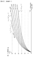
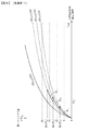
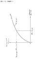
図6は、種々の階調値の映像信号VDSigに基づいて表示素子10を動作させたときの累積動作時間tAOPと、経時変化による表示素子10の黒レベル経時変化量との関係を説明するための模式的なグラフである。
FIG. 6 illustrates the relationship between the accumulated operation time t AOP when the
図6のグラフについて具体的に説明する。初期状態の表示装置1を用いて、表示領域に含まれる第1番目乃至第6番目の領域を、それぞれ、階調値50,100,200,300,400,500の映像信号VDSigに基づいて動作させ、一定時間(例えば1時間)毎に、黒レベル経時変化量ΔVDBSを測定した。尚、黒レベル経時変化量ΔVDBSは、映像信号VDSigの階調値を変えて確認したが、この作業に要する時間は全体の動作時間に比べて充分短い。従って、表示装置1は実質的に継続して階調値50,100,200,300,400,500の映像信号VDSigに基づいて動作したといえる。
The graph of FIG. 6 will be specifically described. Using the
そして、累積動作時間tAOPの長さを横軸の値とし、区分した各領域における表示素子10について、黒レベル経時変化量ΔVDBSの値を縦軸の値としてプロットした。尚、映像信号VDSigの階調値を上述した各階調値に保持する必要があるため、図1に示す輝度補正部110は動作させずに、上述した各階調値の映像信号VDSigを別回路で生成して信号出力回路102に供給して測定を行った。
Then, the length of the accumulated operation time t AOP the value of the horizontal axis, the
図6に示すグラフから明らかなように、映像信号VDSigの階調値が大きいほど、黒レベル経時変化量ΔVDBSは大きくなる。同様に、累積動作時間tAOPが長くなるほど、黒レベル経時変化量ΔVDBSは大きくなる。 As apparent from the graph shown in FIG. 6, the larger the gray level of the video signal VD Sig, the black level time variation .DELTA.VD BS increases. Similarly, as the accumulated operation time t AOP increases, the black level time variation .DELTA.VD BS increases.
測定した結果によれば、図6に示すグラフは、基本的には、累積動作時間tAOPを変数とする対数関数のグラフで近似できることが分かった。逆に言えば、表示素子10は、このような条件を満たすような経時変化をしていることが認められた。
According to the measurement results, it was found that the graph shown in FIG. 6 can basically be approximated by a logarithmic function graph having the cumulative operation time t AOP as a variable. Conversely, it was recognized that the
具体的には、階調値50のときにはΔVDBS=a50・ln(tAOP+1)、階調値100のときにはΔVDBS=a100・ln(tAOP+1)、階調値200のときにはΔVDBS=a200・ln(tAOP+1)といった関数に基づいて、黒レベル経時変化量ΔVDBSを計算することができる。同様に、階調値300のときにはΔVDBS=a300・ln(tAOP+1)、階調値400のときにはΔVDBS=a400・ln(tAOP+1)、階調値500のときにはΔVDBS=a500・ln(tAOP+1)といった関数に基づいて、黒レベル経時変化量ΔVDBSを計算することができる。尚、図示の都合上、図6では階調値100,200,300の関数の記載を省略した。 Specifically, ΔVD BS = a 50 · ln (t AOP +1) when the gradation value is 50 , ΔVD BS = a 100 · ln (t AOP +1) when the gradation value is 100, and ΔVD when the gradation value is 200. The black level temporal change ΔVD BS can be calculated based on a function such as BS = a 200 · ln (t AOP +1). Similarly, when the gradation value is 300, ΔVD BS = a 300 · ln (t AOP +1), when the gradation value is 400, ΔVD BS = a 400 · ln (t AOP +1), and when the gradation value is 500, ΔVD BS = based on a function such as a 500 · ln (t AOP +1 ), it is possible to calculate the black level time variation .DELTA.VD BS. For convenience of illustration, the description of the functions of the gradation values 100, 200, and 300 is omitted in FIG.
ここで、係数「a50」乃至「a500」は正値であり、その値は実測によって定まる。これらの係数は、a50<a100<a200<a300<a400<a500といった大小関係にある。 Here, the coefficients “a 50 ” to “a 500 ” are positive values, and the values are determined by actual measurement. These coefficients have a magnitude relationship of a 50 <a 100 <a 200 <a 300 <a 400 <a 500 .
従って、表示素子10における黒レベル経時変化量は、表示素子10が動作するときの映像信号VDSigの階調値と、その動作時間の長さとによって左右される。映像信号VDSigの階調値を変えて表示素子10を動作させたときの経時変化について、図7を参照して説明する。
Therefore, the amount of black level change with time in the
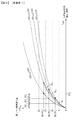
図7は、映像信号VDSigの階調値を変えながら表示素子10を動作させたときの、動作時間と経時変化による表示素子10の黒レベル経時変化量との関係を説明するための模式的なグラフである。
FIG. 7 is a schematic diagram for explaining the relationship between the operating time and the black level change with time of the
具体的には、図7に示すグラフは、初期状態の表示装置1を用いて、動作時間DT1の間は階調値50、動作時間DT2の間は階調値100、動作時間DT3の間は階調値200の映像信号VDSigに基づいて表示素子10を動作さたときのデータに基づいて、累積動作時間の長さを横軸の値とし、表示素子10における黒レベル経時変化量ΔVDBSの値をプロットしたグラフである。尚、図6において説明したと同様に、図1に示す輝度補正部110は動作させずに、上述した各階調値の映像信号VDSigを別回路で生成して信号出力回路102に供給して測定を行った。
Specifically, the graph shown in Figure 7, by using the
図7において、符号PT1,PT2,PT3は、その時点における累積動作時間の値を示す。時間PT3は、動作時間DT1乃至動作時間DT3の長さの総和となる。 In FIG. 7, symbols PT 1 , PT 2 , and PT 3 indicate the values of the accumulated operation time at that time. The time PT 3 is the sum of the lengths of the operation time DT 1 to the operation time DT 3 .
図7において、時間PT1,PT2,PT3に対応する縦軸の値を、それぞれ、RA(PT1),RA(PT2),RA(PT3)と表す。また、図7に示すグラフについて、時間0から時間PT1までの部分、時間PT1から時間PT2までの部分、時間PT2から時間PT3までの部分を、符号CL1,CL2,CL3で表す。図7に示すグラフは、図6に示すグラフの一部を適宜繋げたものとして説明することができる。
In FIG. 7, the values on the vertical axis corresponding to the times PT 1 , PT 2 , and PT 3 are represented as RA (PT 1 ), RA (PT 2 ), and RA (PT 3 ), respectively. Further, in the graph shown in FIG. 7, a portion from
図8は、図7において符号CL1,CL2,CL3で表したグラフの部分と、図6に示すグラフとの対応関係を説明するための図である。 FIG. 8 is a diagram for explaining the correspondence relationship between the graph parts denoted by reference characters CL 1 , CL 2 , and CL 3 in FIG. 7 and the graph shown in FIG.
図8に示すように、図7の符号CL1で表すグラフの部分は、図6における階調値50のグラフにおいて、縦軸が1からRA(PT1)となるまでの部分に対応する。符号CL2で表すグラフの部分は、図6における階調値100のグラフにおいて、縦軸がRA(PT1)からRA(PT2)となるまでの部分に対応する。符号CL3で表すグラフの部分は、図6における階調値200のグラフにおいて、縦軸がRA(PT2)からRA(PT3)となるまでの部分に対応する。
As shown in FIG. 8, the portion of the graph represented by reference sign CL 1 in FIG. 7 corresponds to the portion from 1 to RA (PT 1 ) on the vertical axis in the graph of
一方、図7に示す時間PT3での表示素子10の経時変化は、時間0から時間PT3’まで階調値500の映像信号VDSigに基づいて表示素子10を動作させたと仮定したときの、表示素子10の経時変化に相当する。尚、時間PT3’は、図6に示す階調値500のグラフにおいて、縦軸の値がRA(PT3)となるときの累積基準動作時間である。
On the other hand, the change with time of the
従って、図7に示す動作履歴に基づいて時間PT3’(累積基準動作時間)の値を計算することができれば、この時間PT3’の値と、図6に示す階調値500のカーブとに基づいて、図7に示す時間PT3における表示素子10の黒レベル経時変化量を求めることができる。
Therefore, if the value of the time PT 3 ′ (cumulative reference operation time) can be calculated based on the operation history shown in FIG. 7, the value of this time PT 3 ′ and the curve of the
累積基準動作時間PT3’は、図7に示す動作時間DT1乃至動作時間DT3の長さと、映像信号VDSigの階調値を反映した所定の係数(動作時間換算係数)とに基づいて、計算することができる。図9乃至図12を参照して、動作時間換算係数について説明する。 The accumulated reference operation time PT 3 ′ is based on the length of the operation time DT 1 to the operation time DT 3 shown in FIG. 7 and a predetermined coefficient (operation time conversion coefficient) reflecting the gradation value of the video signal VD Sig. Can be calculated. The operation time conversion coefficient will be described with reference to FIGS.
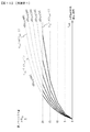
図9は、図7に示す動作履歴に基づいて表示素子10を動作させたときの動作時間の値を、所定の基準階調値、即ち、階調値500の映像信号VDSigに基づいて動作させたと仮定したときの基準動作時間の値に換算する方法を説明するための模式的なグラフである。
FIG. 9 shows the operation time value when the
図9に示す基準動作時間DT1’,DT2’,DT3’は、それぞれ、図7に示す動作時間DT1,DT2,DT3を換算したものに該当する。 The reference operation times DT 1 ′, DT 2 ′, and DT 3 ′ shown in FIG. 9 correspond to values obtained by converting the operation times DT 1 , DT 2 , and DT 3 shown in FIG.
上述したように、図6に示すグラフは対数関数で表される。このため、動作時間DT1,DT2,DT3の値を数学的に基準動作時間DT1’,DT2’,DT3’の値に換算する場合には、冪乗計算を行って換算する必要がある。しかしながら、冪乗計算処理の負荷は非常に重い。従って、例えば1フレーム毎に動作時間の値を基準動作時間値に換算するといった処理を行うことは困難である。 As described above, the graph shown in FIG. 6 is represented by a logarithmic function. For this reason, when mathematically converting the values of the operation times DT 1 , DT 2 , and DT 3 into the values of the reference operation times DT 1 ′, DT 2 ′, and DT 3 ′, conversion is performed by performing a power calculation. There is a need. However, the power of the power calculation process is very heavy. Therefore, for example, it is difficult to perform processing such as converting the operation time value into the reference operation time value for each frame.
そこで、実施例1では、図6に示すグラフを、表示素子の黒レベル階調値の経時変化の範囲に応じて応じて複数の領域に分け、各領域毎にカーブを直線で近似することによって、冪乗計算を行うことなく動作時間の値を基準動作時間値に換算する。尚、実施例1では、黒レベル経時変化量に応じて4つの領域に分けるとして説明するが、領域の分割数はこれに限るものではない。領域の分割数は、表示装置の設計に応じて適宜設定することができる。また、説明の都合上、表示装置1の実使用上の黒レベル経時変化量は、上述した範囲内に収まるものとする。
Accordingly, in the first embodiment, the graph shown in FIG. 6 is divided into a plurality of regions according to the time-dependent change range of the black level gradation value of the display element, and the curve is approximated by a straight line for each region. The value of the operation time is converted into the reference operation time value without performing the power calculation. In the first embodiment, it is described that the area is divided into four areas according to the black level change with time. However, the number of divisions of the area is not limited to this. The number of area divisions can be set as appropriate according to the design of the display device. Further, for convenience of explanation, it is assumed that the black level temporal change amount in actual use of the
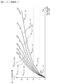
図10は、図6に示すグラフを4つの領域に分割し、各領域毎に直線を用いて近似したグラフである。 FIG. 10 is a graph obtained by dividing the graph shown in FIG. 6 into four regions and approximating each region using a straight line.
具体的には、黒レベル経時変化量ΔVDBSが0以上5未満、5以上10未満、10以上15未満、15以上20未満の4つの領域に分け、各領域のグラフを、領域の境界部の点同士をつなぐ直線を用いて近似した。尚、例えば、領域の中央部における微分係数を傾きとする直線を用いて近似してもよい。 Specifically, less than 5 black level time variation .DELTA.VD BS is 0 or more, 5 or more and less than 10, less than 10 or more 15, divided into four regions of less than 15 or more 20, the graph of each region, the region of the boundary portion of the Approximation was performed using a straight line connecting points. For example, the approximation may be performed using a straight line having a differential coefficient at the center of the region as an inclination.
図11は、図10に示すグラフの傾きを説明するための図である。尚、図示の都合上、図10に対し縦軸及び横軸を1.5倍に拡大して表した。 FIG. 11 is a diagram for explaining the inclination of the graph shown in FIG. For the convenience of illustration, the vertical axis and the horizontal axis are enlarged 1.5 times with respect to FIG.
階調値が50である場合に、黒レベル経時変化量ΔVDBSが0以上5未満であるときの直線の傾きをSL[0,5)_[50]と表し、ΔVDBSが5以上10未満であるときの直線の傾きをSL[5,10)_[50]と表し、ΔVDBSが10以上15未満であるときの直線の傾きをSL[10,15)_[50]と表し、ΔVDBSが15以上20未満であるときの直線の傾きをSL [15,20)_[50] と表す。階調値が100,200,300,400,500の場合は、[]内の階調値を適宜読みかえればよい。これらの傾きは、黒レベル階調値の経時変化の速度を表す。尚、図示の都合上、図11においては、一部の傾きの記載を省略した。
When the gradation value is 50, the slope of the straight line when the black level change amount ΔVD BS is 0 or more and less than 5 is represented as SL [0,5) _ [50], and ΔVD BS is 5 or more and less than 10 Is represented as SL [5,10) _ [50] , ΔVD BS is represented as
図12は、基準動作時間を計算する方法を説明するための模式図である。 FIG. 12 is a schematic diagram for explaining a method of calculating the reference operation time.
例えば、表示素子10が或る時刻tから時刻(t+Δt)までの間、階調値50の映像信号VDSigに基づいて動作したとする。時刻tにおける黒レベル経時変化量をΔVDBS(t)と表し、時刻(t+Δt)における黒レベル経時変化量をΔVDBS(t+Δt)と表す。尚、説明の都合上、0≦ΔVDBS(t),ΔVDBS(t+Δt)<5であるとする。
For example, it is assumed that the
階調値50の映像信号VDSigに基づいて動作した時間Δtにおける黒レベル経時変化量の変化量は、(ΔVDBS(t+Δt)−ΔVDBS(t))である。図12に示すように、この変化量は、表示素子10が階調値500の映像信号VDSigに基づいて時間Δt’の間動作したと仮定したときの変化量に等しい。時間Δtは表示素子10の動作時間に対応し、時間Δt’は基準動作時間に対応する。
The change amount of the black level temporal change amount during the time Δt operated based on the video signal VD Sig having the
時間Δt’は、階調値50の近似直線の傾きSL[0,5)_[50]と、階調値500の近似直線の傾きSL[0,5)_[500]とを用いて、
Δt’=Δt・(SL[0,5)_[50]/SL[0,5)_[500])
といった計算で求めることができる。この(SL[0,5)_[50]/SL[0,5)_[500])は、黒レベル経時変化量が0以上5未満であるときの、階調値50における動作時間換算係数に該当する。
The time Δt ′ is calculated by using the slope SL [0,5) _ [50] of the approximate line having the gradation value 50 and the slope SL [0,5) _ [500] of the approximate line having the
Δt ′ = Δt · (SL [0,5) _ [50] / SL [0,5) _ [500] )
It can be calculated by such a calculation. This (SL [0,5) _ [50] / SL [0,5) _ [500] ) is an operation time conversion coefficient at a gradation value of 50 when the black level change over time is 0 or more and less than 5. It corresponds to.
同様に、例えば、階調値100における動作時間換算係数は(SL[0,5)_[100]/SL[0,5)_[500])で与えられる。即ち、黒レベル経時変化量が0以上5未満であるとき、階調値50,100,200,300,400,500における動作時間換算係数は、(SL[0,5)_[50]/SL[0,5)_[500]),(SL[0,5)_[100]/SL[0,5)_[500]),(SL[0,5)_[200]/SL[0,5)_[500]),(SL[0,5)_[300]/SL[0,5)_[500]),(SL[0,5)_[400]/SL[0,5)_[500]),(SL[0,5)_[500]/SL[0,5)_[500])で与えられる。
Similarly, for example, the operation time conversion coefficient at the
そして、黒レベル経時変化量が5以上10未満であるとき、階調値50,100,200,300,400,500における動作時間換算係数は、(SL[5,10)_[50]/SL[5,10)_[500]),(SL[5,10)_[100]/SL[5,10)_[500]),(SL[5,10)_[200]/SL[5,10)_[500]),(SL[5,10)_[300]/SL[5,10)_[500]),(SL[5,10)_[400]/SL[5,10)_[500]),(SL[5,10)_[500]/SL[5,10)_[500])で与えられる。 When the black level change with time is 5 or more and less than 10, the operation time conversion coefficient at the gradation values 50, 100, 200, 300, 400, 500 is (SL [5,10) _ [50] / SL. [5,10) _ [500] ), (SL [5,10) _ [100] / SL [5,10) _ [500] ), (SL [5,10) _ [200] / SL [5 , 10) _ [500] ), (SL [5,10) _ [300] / SL [5,10) _ [500] ), (SL [5,10) _ [400] / SL [5,10 ) _ [500] ), (SL [5,10) _ [500] / SL [5,10) _ [500] ).
また、黒レベル経時変化量が10以上15未満であるとき、階調値50,100,200,300,400,500における動作時間換算係数は、(SL[10,15)_[50]/SL[10,15)_[500]),(SL[10,15)_[100]/SL[10,15)_[500]),(SL[10,15)_[200]/SL[10,15)_[500]),(SL[10,15)_[300]/SL[10,15)_[500]),(SL[10,15)_[400]/SL[10,15)_[500]),(SL[10,15)_[500]/SL[10,15)_[500])で与えられる。 When the black level change with time is 10 or more and less than 15, the operation time conversion coefficient at the gradation values 50, 100, 200, 300, 400, 500 is (SL [10,15) _ [50] / SL. [10,15) _ [500] ), (SL [10,15) _ [100] / SL [10,15) _ [500] ), (SL [10,15) _ [200] / SL [10 , 15) _ [500] ), (SL [10,15) _ [300] / SL [10,15) _ [500] ), (SL [10,15) _ [400] / SL [10,15 ) _ [500] ), (SL [10,15) _ [500] / SL [10,15) _ [500] ).
また、黒レベル経時変化量が15以上20未満であるとき、階調値50,100,200,300,400,500における動作時間換算係数は、(SL[15,20)_[50]/SL[15,20)_[500]),(SL[15,20)_[100]/SL[15,20)_[500]),(SL[15,20)_[200]/SL[15,20)_[500]),(SL[15,20)_[300]/SL[15,20)_[500]),(SL[15,20)_[400]/SL[15,20)_[500]),(SL[15,20)_[500]/SL[15,20)_[500])で与えられる。 When the black level change with time is 15 or more and less than 20, the operation time conversion coefficient at the gradation values 50, 100, 200, 300, 400, 500 is (SL [15,20) _ [50] / SL. [15,20) _ [500] ), (SL [15,20) _ [100] / SL [15,20) _ [500] ), (SL [15,20) _ [200] / SL [15 , 20) _ [500] ), (SL [15,20) _ [300] / SL [15,20) _ [500] ), (SL [15,20) _ [400] / SL [15,20 ) _ [500] ), (SL [15,20) _ [500] / SL [15,20) _ [500] ).
横軸を映像信号VDSigの階調値とし、縦軸を動作時間換算係数としてプロットすると、黒レベル経時変化量の範囲の種類分の本数のグラフが得られる。図13は、映像信号VDSigの階調値と動作時間換算係数との関係を示すグラフである。 Plotting the horizontal axis as the gradation value of the video signal VD Sig and the vertical axis as the operation time conversion coefficient gives a graph of the number of types in the range of the black level temporal change amount. FIG. 13 is a graph showing the relationship between the gradation value of the video signal VD Sig and the operating time conversion coefficient.
図13において、符号[0,5)を付したグラフは、黒レベル経時変化量が0以上5未満のときのグラフであり、符号[5,10)を付したグラフは、黒レベル経時変化量が5以上10未満のときのグラフである。同様に、符号[10,15)を付したグラフは、黒レベル経時変化量が10以上15未満のときのグラフであり、符号[15,20)を付したグラフは、黒レベル経時変化量が15以上20未満のときのグラフである。 In FIG. 13, the graph with the reference [0, 5) is a graph when the black level change over time is 0 or more and less than 5, and the graph with the reference [5, 10) shows the black level change over time. Is a graph when 5 is less than 10. Similarly, the graph with the reference [10, 15) is a graph when the black level change with time is 10 or more and less than 15, and the graph with the reference [15, 20) has a change with time of the black level. It is a graph when it is 15 or more and less than 20.
以上、動作時間換算係数について説明した。動作時間換算係数を用いた基準動作時間の計算方法は以下のとおりである。 The operation time conversion coefficient has been described above. The calculation method of the reference operation time using the operation time conversion coefficient is as follows.
図9に示す基準動作時間DT1’は、その始期において黒レベル経時変化量が0以上5未満であるから、動作時間換算係数として(SL[0,5)_[50]/SL[0,5)_[500])を用いて、
DT1’=DT1・(SL[0,5)_[50]/SL[0,5)_[500])
といった計算で求めることができる。
The reference operation time DT 1 ′ shown in FIG. 9 has a black level change over time of 0 or more and less than 5 at the beginning, and therefore, (SL [0,5) _ [50] / SL [0, 5) _ [500] )
DT 1 '= DT 1 · (SL [0,5) _ [50] / SL [0,5) _ [500] )
It can be calculated by such a calculation.
同様に、基準動作時間DT2’は、その始期において黒レベル経時変化量が5以上10未満であるから、動作時間換算係数として(SL[5,10)_[100]/SL[5,10)_[500])を用いて、
DT2’=DT2・(SL[5,10)_[100]/SL[5,10)_[500])
といった計算で求めることができる。
Similarly, the reference operation time DT 2 ′ has a black level aging change amount of 5 or more and less than 10 at the beginning thereof, so that the operation time conversion coefficient is (SL [5,10) _ [100] / SL [5,10 ) _ [500] )
DT 2 '= DT 2 · (SL [5,10) _ [100] / SL [5,10) _ [500] )
It can be calculated by such a calculation.
また、基準動作時間DT3’は、その始期において黒レベル経時変化量が10以上15未満であるから、動作時間換算係数として(SL[10,15)_[200]/SL[10,15)_[500])を用いて、
DT3’=DT3・(SL[10,15)_[200]/SL[10,15)_[500])
といった計算で求めることができる。
Further, since the black level aging change amount is 10 or more and less than 15 at the beginning of the reference operation time DT 3 ′, the operation time conversion coefficient is (SL [10,15) _ [200] / SL [10,15). _ [500] )
DT 3 '= DT 3 · (SL [10,15) _ [200] / SL [10,15) _ [500] )
It can be calculated by such a calculation.
そして、累積基準動作時間PT3’は、基準動作時間DT1’,DT2’,DT3’の総和として求めることができる。 The accumulated reference operation time PT 3 ′ can be obtained as the sum of the reference operation times DT 1 ′, DT 2 ′, and DT 3 ′.
尚、図9等にあっては、図示の都合上、動作時間DT1,DT2,DT3を1フレーム期間に対して極端に長い時間として表した。このため、図にあっては、各動作時間の前端と後端とで、黒レベル経時変化量が異なる範囲に含まれるように表されている。実際には、動作時間の長さを例えば1フレーム期間とすれば、その前後での黒レベル経時変化量の変化は僅かである。 In FIG. 9 and the like, for the convenience of illustration, the operation times DT 1 , DT 2 , and DT 3 are represented as extremely long times with respect to one frame period. For this reason, in the figure, the black level change with time is included in different ranges at the front end and the rear end of each operation time. Actually, if the length of the operation time is, for example, one frame period, the change in the black level temporal change amount before and after that is slight.
次いで図2、図14乃至図18を参照して、表示装置1の焼き付きを軽減する駆動方法について説明する。
Next, a driving method for reducing burn-in of the
図14は、図2に示す動作時間換算係数格納部113に格納されているデータを説明するための模式的なグラフである。
FIG. 14 is a schematic graph for explaining data stored in the operation time conversion
図2に示す輝度補正部110の概要については既に述べたが、動作時間換算係数格納部113には、表示素子10の黒レベル階調値の経時変化の範囲毎に対応した複数の動作時間換算係数テーブルが格納されている。具体的には、図14のグラフに示す関係を表す関数fCSC_BS1,fCSC_BS2,fCSC_BS3,fCSC_BS4がテーブルとして予め格納されている。これは、図13に示す映像信号VDSigの階調値と動作時間換算係数との関係を反映したものである。関数fCSC_BS1は黒レベルシフト量が0以上5未満のときの関係を表し、関数fCSC_BS2は黒レベルシフト量が5以上10未満のときの関係を表し、関数fCSC_BS3は黒レベルシフト量が10以上15未満のときの関係を表し、関数fCSC_BS4は黒レベルシフト量が15以上20未満のときの関係を表す。
Although the outline of the
図15は、図2に示す累積基準動作時間値保持部114に保持されるデータを説明するための模式図である。
FIG. 15 is a schematic diagram for explaining data held in the accumulated reference operation time
上述したように、累積基準動作時間値保持部114は、各表示素子10に対応した記憶領域を持ち、書き換え可能な不揮発性の記憶装置から構成されており、累積基準動作時間値を示すデータSP(1,1)乃至SP(N,M)を保持する。
As described above, the accumulated reference operation time
図16は、図2に示す基準カーブ格納部116に格納されているデータを説明するための模式的なグラフである。
FIG. 16 is a schematic graph for explaining data stored in the reference
基準カーブ格納部116には、図16に示す基準カーブを表す関数fREF_BS_SHIFTがテーブルとして予め格納されている。この基準カーブは、図6において階調値500であるときのカーブを表すものである。
In the reference
図18は、図2に示す黒レベルシフト量保持部115を構成する黒レベルシフト量格納部115Bに保持されるデータを説明するための模式図である。
FIG. 18 is a schematic diagram for explaining data held in the black level shift
上述したように、黒レベルシフト量格納部115Bは、各表示素子10に対応した記憶領域を持ち、書き換え可能な不揮発性の記憶装置から構成されており、黒レベルシフト量を示すデータLC(1,1)乃至LC(N,M)を保持する。
As described above, the black level shift
実施例1の駆動方法は、輝度補正部110の動作に基づいて、入力信号vDSigの階調値を補正して映像信号VDSigとして出力することによって、表示パネル20が画像を表示する際の表示素子10の輝度を補正する輝度補正ステップを有し、
輝度補正ステップは、
表示素子10が映像信号VDSigに基づいて所定の単位時間の間動作したときの黒レベル階調値の経時変化と、表示素子10が所定の基準階調値の映像信号VDSigに基づいて動作したと仮定したときの表示素子10の黒レベル階調値の経時変化とが等しくなる基準動作時間の値を計算する基準動作時間値計算ステップ、
基準動作時間の値を表示素子10毎に累積した累積基準動作時間値を保持する累積基準動作時間値保持ステップ、
累積基準動作時間値と、表示素子10が所定の基準階調値の映像信号VDSigに基づいて動作したときの表示素子10の動作時間と表示素子10の黒レベル階調値の経時変化との関係を示す基準カーブとを参照して表示素子10の黒レベル階調値の経時変化を補償するための黒レベルシフト量を計算し、各表示素子10に対応した黒レベルシフト量を保持する黒レベルシフト量保持ステップ、及び、
黒レベルシフト量に基づいて、各表示素子10に対応した入力信号vDSigの階調値を補正して映像信号VDSigとして出力する映像信号生成ステップ、
を備えている。
In the driving method of the first embodiment, the
The brightness correction step
The time-dependent change of the black level gradation value when the
An accumulated reference operation time value holding step for holding an accumulated reference operation time value obtained by accumulating the value of the reference operation time for each
The accumulated reference operation time value, the operation time of the
A video signal generation step of correcting the gradation value of the input signal vD Sig corresponding to each
It has.
ここでは、表示装置1の初期状態から累積して第1番目乃至第(Q−1)番目のフレーム表示が終了し、第Q番目(但し、Qは2以上の自然数)のフレーム表示を行うための書き込み処理が行われる際の、第(n,m)番目の表示素子10に関する輝度補正ステップについて説明する。
Here, since the first to (Q-1) th frame display is completed from the initial state of the
尚、第(n,m)番目の表示素子10の第q番目(但し、q=1,2・・・,Q)のフレームにおける入力信号vDSig及び映像信号VDSigを、vDSig(n,m)_q及びVDSig(n,m)_qと表し、第q番目のフレーム表示が表示した時点での、第(n,m)番目の表示素子10に対応する累積基準動作時間値を示すデータをSP(n,m)_qと表し、第(n,m)番目の表示素子10に対応する黒レベルシフト量を示すデータをLC(n,m)_qと表す。また、所謂1フレーム期間が占める時間を符号TFで表す。尚、初期状態にあっては、データSP(1,1)乃至SP(N,M)、及び、データLC(1,1)乃至LC(N,M)には初期値として予め「0」が格納されている。
The input signal vD Sig and the video signal VD Sig in the q-th (where q = 1, 2,..., Q) frame of the (n, m) -
第(Q−1)番目の表示フレームにおいて、図2に示す基準動作時間値計算部112は、映像信号VDSig(n,m)_Q-1、及び、黒レベルシフト量格納部のデータLC(n,m)_Q-2に基づいて、基準動作時間値計算ステップを行う。
In the (Q-1) th display frame, the reference operation time
具体的には、基準動作時間値計算部112は、黒レベルシフト量保持部115に保持された黒レベルシフト量LC(n,m)_Q-2の値に対応して動作時間換算係数テーブルを選択して参照する。具体的には、LC(n,m)_Q-2の値が0以上5未満のときには関数fCSC_BS1を選択し、LC(n,m)_Q-2の値が5以上10未満のときには関数fCSC_BS2を選択し、LC(n,m)_Q-2の値が10以上15未満のときには関数fCSC_BS3を選択し、LC(n,m)_Q-2の値が15以上20未満のときには関数fCSC_BS4を選択する。そして、
第(Q−1)番目の表示フレームにおける基準動作時間=TF・fCSC_BS(VDSig(n,m)_Q-1)
といった計算を行う。尚、記載の都合上、上式においては選択した関数を単にfCSC_BSとして表した。
Specifically, the reference operation time
Reference operation time in the (Q-1) th display frame = TF · f CSC_BS (VD Sig (n, m) _Q-1 )
The calculation is performed. For convenience of description, the selected function is simply expressed as f CSC_BS in the above equation.
そして、累積基準動作時間値保持部114は、基準動作時間値計算部112が計算した基準動作時間の値を表示素子10毎に累積した累積基準動作時間値を保持する累積基準動作時間値保持ステップを行う。
Then, the accumulated reference operation time
具体的には、第(Q−1)番目の表示フレームにおいて、累積基準動作時間値保持部114は、直前のデータSP(n,m)_Q-2に対し、更に、上述した第(Q−1)番目の表示フレームにおける基準動作時間を加算する。具体的には、
SP(n,m)_Q-1=SP(n,m)_Q-2+TF・fCSC_BS(VDSig(n,m)_Q-1)
といった動作を行う。これにより、累積基準動作時間値保持部114には、基準動作時間値計算部112が計算した基準動作時間の値を表示素子10毎に累積した累積基準動作時間値が保持される。
Specifically, in the (Q-1) -th display frame, the accumulated reference operation time
SP (n, m) _Q-1 = SP (n, m) _Q-2 + TF / f CSC_BS (VD Sig (n, m) _Q-1 )
The operation is performed. As a result, the accumulated reference operation time
そして、黒レベルシフト量保持部115は、各表示素子10に対応した黒レベルシフト量を保持する黒レベルシフト量保持ステップを行う。
Then, the black level shift amount holding unit 115 performs a black level shift amount holding step for holding the black level shift amount corresponding to each
図17は、図2に示す黒レベルシフト量保持部115を構成する黒レベルシフト量計算部115Aの動作を説明するための模式的なグラフである。
FIG. 17 is a schematic graph for explaining the operation of the black level shift
具体的には、黒レベルシフト量計算部115Aは、累積基準動作時間値保持部114に保持されたデータSP(n,m)_Q-1に基づいて基準カーブ格納部116を参照し(図17参照)、関数値fREF_BS_SHIFT(SP(n,m)_Q-1)を求める。そして、黒レベルシフト量ΔVDBS_SHIFTとして、関数値fREF_BS_SHIFT(SP(n,m)_Q-1)を、黒レベルシフト量格納部115BのデータLC(n,m)_Q-1に保持する。
Specifically, the black level shift
そして、映像信号生成部111は、黒レベルシフト量ΔVDBS_SHIFTに基づいて、各表示素子10に対応した入力信号vDSigの階調値を補正して映像信号VDSigとして出力する映像信号生成ステップを行う。
The video
即ち、第Q番目のフレームの直前には、累積基準動作時間値保持部114には、データSP(1,1)_Q-1乃至SP(N,M)_Q-1が保持され、黒レベルシフト量保持部115を構成する黒レベルシフト量格納部115Bには、データLC(1,1)_Q-1乃至LC(N,M)_Q-1が保持されている。
That is, immediately before the Q-th frame, the accumulated reference operation time
映像信号生成部111は、入力信号vDSig(n,m)_Qと黒レベルシフト量格納部115BのデータLC(n,m)_Q-1とを参照し、
映像信号VDSig(n,m)_Q=vDSig(n,m)_Q+LC(n,m)_Q-1
といった計算を行い、生成した映像信号VDSig(n,m)_Qを信号出力回路102に供給する。
The video
Video signal VD Sig (n, m) _Q = vD Sig (n, m) _Q + LC (n, m) _Q-1
The generated video signal VD Sig (n, m) _Q is supplied to the
そして、第Q番目のフレーム表示が行われる。その後、第(Q+1)番目以降のフレームにおいても、上述した動作が繰り返される。 Then, the Qth frame display is performed. Thereafter, the above-described operation is repeated in the (Q + 1) th and subsequent frames.
実施例1の表示装置1にあっては、動作時間換算係数格納部113を参照して基準動作時間の値を算出し、その値を累積基準動作時間値として保持し、これに基づいて基準カーブ格納部116を参照して黒レベルシフト量を求める。基準動作時間の値には、映像信号VDSigの階調値が反映されている。また、基準動作時間の値は、単純な乗算処理によって求めることができるので、高速な処理を行うことができる。
In the
基準動作時間の値を累積した累積基準動作時間値には、映像信号VDSigの階調値の履歴が反映されている。これにより、黒レベルを示す階調値の経時変化に起因する焼き付きが軽減され、良好な画像を表示することができる。 The accumulated reference operation time value obtained by accumulating the reference operation time value reflects the history of gradation values of the video signal VD Sig . As a result, the burn-in caused by the temporal change of the gradation value indicating the black level is reduced, and a good image can be displayed.
以上の説明において、表示装置1はモノクロ表示としたが、カラー表示の表示装置であってもよい。この場合において、例えば、表示素子10の経時変化の傾向が発光色毎に異なるといった場合には、図2に示す動作時間換算係数格納部113及び基準カーブ格納部116を、発光色毎に別個の構成としておけばよい。
In the above description, the
以上、表示装置1における焼き付きの軽減について詳しく説明した。
The burn-in reduction in the
次いで、第(n,m)番目の表示素子10についての、黒レベルを示す階調値の経時変化の補正以外の動作全般の詳細を、図19、図20の(A)及び(B)、図21の(A)及び(B)、図22の(A)及び(B)、図23の(A)及び(B)、図24の(A)及び(B)、並びに、図25を参照して詳細に説明する。尚、これらの図面や以下の説明においては、記載の都合上、第(n,m)番目の表示素子10に対応する映像信号電圧VSig(n,m)を、VSig_mと表す。
Next, details of the overall operation of the (n, m) -
[期間−TP(2)-1](図19、図20の(A)参照)
この[期間−TP(2)-1]は、例えば、前の表示フレームにおける動作であり、前回の各種の処理完了後に第(n,m)番目の表示素子10が発光状態にある期間である。即ち、第(n,m)番目の画素を構成する表示素子10における発光部ELPには、後述する式(5’)に基づくドレイン電流Ids’が流れており、第(n,m)番目の画素を構成する表示素子10の輝度は、係るドレイン電流Ids’に対応した値である。ここで、書込みトランジスタTRWは非導通状態であり、駆動トランジスタTRDは導通状態である。第(n,m)番目の表示素子10の発光状態は、第(m+m’)行目に配列された表示素子10の水平走査期間の開始直前まで継続される。
[Period -TP (2) −1 ] (see FIGS. 19 and 20A)
This [period-TP (2) −1 ] is, for example, an operation in the previous display frame, and is a period in which the (n, m)
上述したように、各水平走査期間に対応して、データ線DTLnには、基準電圧VOfsと映像信号電圧VSigとが供給される。しかしながら、書込みトランジスタTRWは非導通状態であるので、[期間−TP(2)-1]においてデータ線DTLnの電位(電圧)が変化しても、第1ノードND1と第2ノードND2の電位は変化しない(実際には、寄生容量等の静電結合による電位変化が生じ得るが、通常、これらは無視することができる)。後述する[期間−TP(2)0]においても同様である。 As described above, the reference voltage V Ofs and the video signal voltage V Sig are supplied to the data line DTL n corresponding to each horizontal scanning period. However, since the write transistor TR W is in a non-conductive state, even if the potential (voltage) of the data line DTL n changes in [period -TP (2) −1 ], the first node ND 1 and the second node ND The potential of 2 does not change (actually, a potential change due to electrostatic coupling such as parasitic capacitance may occur, but these can usually be ignored). The same applies to [period-TP (2) 0 ] described later.
図19に示す[期間−TP(2)0]〜[期間−TP(2)6]は、前回の各種の処理完了後の発光状態が終了した後から、次の書込み処理が行われる直前までの動作期間である。[期間−TP(2)0]〜[期間−TP(2)7]において、第(n,m)番目の表示素子10は原則として非発光状態にある。図19に示すように、[期間−TP(2)5]、[期間−TP(2)6]及び[期間−TP(2)7]は第m番目の水平走査期間Hmに包含される。
[Period-TP (2) 0 ] to [Period-TP (2) 6 ] shown in FIG. 19 are from the end of the light emission state after completion of the previous various processes to immediately before the next writing process is performed. Is the operation period. In [Period-TP (2) 0 ] to [Period-TP (2) 7 ], the (n, m)
また、[期間−TP(2)3]及び[期間−TP(2)5]において、走査線SCLからの走査信号に基づいて導通状態とされた書込みトランジスタTRWを介してデータ線DTLnから駆動トランジスタTRDのゲート電極に基準電圧VOfsを印加した状態で、給電線PS1から駆動電圧VCC-Hを駆動トランジスタTRDの一方のソース/ドレイン領域に印加し、以て、駆動トランジスタTRDの他方のソース/ドレイン領域の電位を基準電圧VOfsから駆動トランジスタTRDの閾値電圧を減じた電位に向かって近づける閾値電圧キャンセル処理を行う。 Further, in [Period-TP (2) 3 ] and [Period-TP (2) 5 ], the data line DTL n is connected to the data line DTL n via the write transistor TR W that is turned on based on the scanning signal from the scanning line SCL. In a state where the reference voltage V Ofs is applied to the gate electrode of the drive transistor TR D, the drive voltage V CC-H is applied from the power supply line PS1 to one source / drain region of the drive transistor TR D , and thus the drive transistor TR A threshold voltage canceling process is performed to bring the potential of the other source / drain region of D closer to the potential obtained by subtracting the threshold voltage of the driving transistor TR D from the reference voltage V Ofs .
実施例1においては、閾値電圧キャンセル処理を複数の水平走査期間、より具体的には、第(m−1)番目の水平走査期間Hm-1と第m番目の水平走査期間Hmにおいて行うとして説明するが、これに限定するものではない。 In the first embodiment, the threshold voltage canceling process is performed in a plurality of horizontal scanning periods, more specifically, in the (m−1) th horizontal scanning period H m−1 and the mth horizontal scanning period H m . However, the present invention is not limited to this.
また、[期間−TP(2)1]において、基準電圧VOfsとの差が駆動トランジスタTRDの閾値電圧を超える初期化電圧VCC-Lを給電線PS1から駆動トランジスタTRDの一方のソース/ドレイン領域に印加し、走査線SCLmからの走査信号に基づいて導通状態とされた書込みトランジスタTRWを介してデータ線DTLnから駆動トランジスタTRDのゲート電極に基準電圧VOfsを印加し、以て、駆動トランジスタTRDのゲート電極の電位と駆動トランジスタTRDの他方のソース/ドレイン領域の電位とを初期化する。 In [Period -TP (2) 1 ], the initialization voltage V CC-L whose difference from the reference voltage V Ofs exceeds the threshold voltage of the drive transistor TR D is applied to the one source of the drive transistor TR D from the power supply line PS1. A reference voltage V Ofs is applied from the data line DTL n to the gate electrode of the drive transistor TR D via the write transistor TR W applied to the drain region and made conductive based on the scanning signal from the scanning line SCL m. , following Te initializes the potential of the other of the source / drain regions of the potential and the drive transistor TR D of the gate electrode of the driving transistor TR D.
図19において、[期間−TP(2)1]は、第(m−2)番目の水平走査期間Hm-2における基準電圧期間(データ線DTLに基準電圧VOfsが印加される期間)に一致し、[期間−TP(2)3]は、第(m−1)番目の水平走査期間Hm-1における基準電圧期間に一致し、[期間−TP(2)5]は、第m番目の水平走査期間Hmにおける基準電圧期間に一致するとする。 In FIG. 19, [period-TP (2) 1 ] is a reference voltage period (period in which the reference voltage V Ofs is applied to the data line DTL) in the (m−2) th horizontal scanning period H m−2 . [Period-TP (2) 3 ] coincides with the reference voltage period in the (m−1) th horizontal scanning period H m−1 , and [Period-TP (2) 5 ] Assume that the reference voltage period coincides with the first horizontal scanning period H m .
引き続き、図19等を参照して、[期間−TP(2)0]〜[期間−TP(2)8]の各期間の動作について説明する。 Next, with reference to FIG. 19 and the like, operations in each period of [Period-TP (2) 0 ] to [Period-TP (2) 8 ] will be described.
[期間−TP(2)0](図19、図20の(B)参照)
この[期間−TP(2)0]は、例えば、前の表示フレームから現表示フレームにおける動作である。即ち、この[期間−TP(2)0]は、前の表示フレームにおける第(m+m’)番目の水平走査期間Hm+m'の始期から、現表示フレームにおける第(m−3)番目の水平走査期間の終期までの期間である。そして、この[期間−TP(2)0]において、第(n,m)番目の表示素子10は、原則として非発光状態にある。[期間−TP(2)0]の始期において、電源部100から給電線PS1mに供給する電圧を駆動電圧VCC-Hから初期化電圧VCC-Lに切り替える。その結果、第2ノードND2の電位はVCC-Lまで低下し、発光部ELPのアノード電極とカソード電極との間に逆方向電圧が印加され、発光部ELPは非発光状態となる。また、第2ノードND2の電位低下に倣うように、浮遊状態の第1ノードND1(駆動トランジスタTRDのゲート電極)の電位も低下する。
[Period -TP (2) 0 ] (see FIGS. 19 and 20B)
This [period-TP (2) 0 ] is, for example, an operation from the previous display frame to the current display frame. That is, this [period-TP (2) 0 ] is the (m−3) th in the current display frame from the beginning of the (m + m ′) th horizontal scanning period H m + m ′ in the previous display frame. This is the period up to the end of the horizontal scanning period. In this [period-TP (2) 0 ], the (n, m) -
[期間−TP(2)1](図19、図21の(A)参照)
そして、現表示フレームにおける第(m−2)番目の水平走査期間Hm-2が開始する。この[期間−TP(2)1]において、走査線SCLmをハイレベルとして表示素子10の書込みトランジスタTRWを導通状態とする。信号出力回路102からデータ線DTLnに供給される電圧は基準電圧VOfsである。その結果、第1ノードND1の電位は、VOfs(0ボルト)となる。電源部100の動作に基づき、給電線PS1mから初期化電圧VCC-Lを第2ノードND2に印加しているので、第2ノードND2の電位はVCC-L(−10ボルト)を保持する。
[Period -TP (2) 1 ] (see FIGS. 19 and 21A)
Then, the (m−2) th horizontal scanning period H m−2 in the current display frame starts. In this [period-TP (2) 1 ], the scanning line SCL m is set to the high level, and the writing transistor TR W of the
第1ノードND1と第2ノードND2との間の電位差は10ボルトであり、駆動トランジスタTRDの閾値電圧Vthは3ボルトであるので、駆動トランジスタTRDは導通状態である。尚、第2ノードND2と発光部ELPに備えられたカソード電極との間の電位差は−10ボルトであり、発光部ELPの閾値電圧Vth-ELを超えない。これにより、第1ノードND1の電位及び第2ノードND2の電位が初期化される。 The first node ND 1 and the potential difference between the second node ND 2 is 10 volts, the threshold voltage V th of the driving transistor TR D because it is 3 volts, the driving transistor TR D is conductive. The potential difference between the second node ND 2 and the cathode electrode provided in the light emitting unit ELP is −10 volts, and does not exceed the threshold voltage V th−EL of the light emitting unit ELP. As a result, the potential of the first node ND 1 and the potential of the second node ND 2 are initialized.
[期間−TP(2)2](図19、図21の(B)参照)
この[期間−TP(2)2]において走査線SCLmをローレベルとする。表示素子10の書込みトランジスタTRWは非導通状態となる。第1ノードND1及び第2ノードND2の電位は、基本的には従前の状態を維持する。
[Period -TP (2) 2 ] (see FIGS. 19 and 21B)
In this [period-TP (2) 2 ], the scanning line SCL m is set to the low level. The write transistor TR W of the
[期間−TP(2)3](図19、図22の(A)参照)
この[期間−TP(2)3]において、第1回目の閾値電圧キャンセル処理を行う。走査線SCLmをハイレベルとし表示素子10の書込みトランジスタTRWを導通状態とする。信号出力回路102からデータ線DTLnに供給される電圧は基準電圧VOfsである。第1ノードND1の電位は、VOfs(0ボルト)である。
[Period -TP (2) 3 ] (see FIGS. 19 and 22A)
In this [period-TP (2) 3 ], the first threshold voltage canceling process is performed. The write transistor TR W of the
次いで、電源部100から給電線PS1mに供給される電圧を、電圧VCC-Lから駆動電圧VCC-Hに切り替える。その結果、第1ノードND1の電位は変化しないが(VOfs=0ボルトを維持)、基準電圧VOfsから駆動トランジスタTRDの閾値電圧Vthを減じた電位に向かって、第2ノードND2の電位は変化する。即ち、第2ノードND2の電位が上昇する。
Next, the voltage supplied from the
この[期間−TP(2)3]が充分長ければ、駆動トランジスタTRDのゲート電極と他方のソース/ドレイン領域との間の電位差がVthに達し、駆動トランジスタTRDは非導通状態となる。即ち、第2ノードND2の電位が(VOfs−Vth)に近づき、最終的に(VOfs−Vth)となる。しかしながら、図19に示す例では、[期間−TP(2)3]の長さは、第2ノードND2の電位を充分変化させるには足りない長さであり、[期間−TP(2)3]の終期において、第2ノードND2の電位は、VCC-L<V1<(VOfs−Vth)という関係を満たす或る電位V1に達する。 If this [period-TP (2) 3 ] is sufficiently long, the potential difference between the gate electrode of the drive transistor TR D and the other source / drain region reaches V th , and the drive transistor TR D becomes non-conductive. . That is, the potential of the second node ND 2 approaches (V Ofs -V th), and finally becomes (V Ofs -V th). However, in the example shown in FIG. 19, the length of [Period -TP (2) 3 ] is insufficient to change the potential of the second node ND 2 sufficiently, and [Period -TP (2) 3 ], the potential of the second node ND 2 reaches a certain potential V 1 that satisfies the relationship of V CC-L <V 1 <(V Ofs −V th ).
[期間−TP(2)4](図19、図22の(B)参照)
この[期間−TP(2)4]においては、走査線SCLmをローレベルとし、表示素子10の書込みトランジスタTRWは非導通状態となる。その結果、第1ノードND1は浮遊状態となる。
[Period -TP (2) 4 ] (see FIGS. 19 and 22B)
In this [period-TP (2) 4 ], the scanning line SCL m is set to the low level, and the writing transistor TR W of the
電源部100から駆動トランジスタTRDの一方のソース/ドレイン領域に駆動電圧VCC-Hが印加されているので、第2ノードND2の電位は、電位V1から或る電位V2に上昇する。一方、駆動トランジスタTRDのゲート電極は浮遊状態であり、容量部C1が存在するが故に、ブートストラップ動作が駆動トランジスタTRDのゲート電極に生ずる。従って、第1ノードND1の電位は、第2ノードND2の電位変化に倣って上昇する。
Since the drive voltage V CC-H is applied from the
次の[期間−TP(2)5]における動作の前提として、[期間−TP(2)5]の始期において、第2ノードND2の電位が(VOfs−Vth)よりも低いことが必要となる。[期間−TP(2)4]の長さは、基本的には、V2<(VOfs-L−Vth)の条件を満たすように決定されている。 As a premise of the operation in the next [period-TP (2) 5 ], the potential of the second node ND 2 is lower than (V Ofs −V th ) at the beginning of [period-TP (2) 5 ]. Necessary. The length of [Period -TP (2) 4 ] is basically determined so as to satisfy the condition of V 2 <(V Ofs−L −V th ).
[期間−TP(2)5](図19、図23の(A)及び(B)参照)
この[期間−TP(2)5]において、第2回目の閾値電圧キャンセル処理を行う。走査線SCLmからの走査信号に基づいて、表示素子10の書込みトランジスタTRWを導通状態とする。信号出力回路102からデータ線DTLnに供給される電圧は基準電圧VOfsである。第1ノードND1の電位は、ブートストラップ動作によって上昇した電位から、再度VOfs(0ボルト)となる(図23の(A)参照)。
[Period -TP (2) 5 ] (see FIGS. 19 and 23 (A) and (B))
In this [period-TP (2) 5 ], the second threshold voltage canceling process is performed. Based on the scanning signal from the scanning line SCL m, the writing transistor TR W of the
ここで、容量部C1の値を値c1とし、発光部ELPの容量CELの値を値cELとする。そして、駆動トランジスタTRDのゲート電極と他方のソース/ドレイン領域との間の寄生容量の値をcgsとする。第1ノードND1と第2ノードND2との間の容量値を符号cAで表せば、cA=c1+cgsである。また、第2ノードND2と第2の給電線PS2との間の容量値を符号cBと表せば、cB=cELである。尚、発光部ELPの両端に、追加の容量部が並列に接続されている構成であってもよいが、その場合には、cBには更に追加の容量部の容量値が加算される。 Here, the value of the capacitor C 1 is set as a value c 1, and the value of the capacitor C EL of the light emitting unit ELP is set as a value c EL . The value of the parasitic capacitance between the gate electrode of the driving transistor TR D and the other source / drain region is defined as c gs . If the capacitance value between the first node ND 1 and the second node ND 2 is represented by the symbol c A , c A = c 1 + c gs . In addition, if a capacitance value between the second node ND 2 and the second power supply line PS2 is represented by a symbol c B , c B = c EL . Note that both ends of the light emitting section ELP, although additional capacity portion may have a configuration that is connected in parallel, in which case, further capacitance value of the additional capacitance portion to c B is added.
第1ノードND1の電位が変化すると、第1ノードND1と第2ノードND2との間の電位も変化する。即ち、第1ノードND1の電位の変化分に基づく電荷が、第1ノードND1と第2ノードND2との間の容量値と、第2ノードND2と第2の給電線PS2との間の容量値に応じて、振り分けられる。然るに、値cb(=cEL)が、値cA(=c1+cgs)と比較して充分に大きな値であれば、第2ノードND2の電位の変化は小さい。そして、一般に、発光部ELPの容量CELの値cELは、容量部C1の値c1及び駆動トランジスタTRDの寄生容量の値cgsよりも大きい。以下、第1ノードND1の電位変化により生ずる第2ノードND2の電位変化は考慮せずに説明を行う。尚、図19に示した駆動のタイミングチャートにおいては、第1ノードND1の電位変化により生ずる第2ノードND2の電位変化を考慮せずに示した。
When the potential of the first node ND 1 changes, the potential between the first node ND 1 and the second node ND 2 also changes. That is, the charge based on the change in the potential of the first node ND 1 is caused by the capacitance value between the first node ND 1 and the second node ND 2, and the second node ND 2 and the second
電源部100から駆動トランジスタTRDの一方のソース/ドレイン領域に駆動電圧VCC-Hが印加されているので、基準電圧VOfsから駆動トランジスタTRDの閾値電圧Vthを減じた電位に向かって、第2ノードND2の電位は変化する。即ち、第2ノードND2の電位は、電位V2から上昇し、基準電圧VOfsから駆動トランジスタTRDの閾値電圧Vthを減じた電位に向かって変化する。そして、駆動トランジスタTRDのゲート電極と他方のソース/ドレイン領域との間の電位差がVthに達すると、駆動トランジスタTRDが非導通状態となる(図23の(B)参照)。この状態にあっては、第2ノードND2の電位は、概ね(VOfs−Vth)である。ここで、以下の式(2)が保証されていれば、云い換えれば、式(2)を満足するように電位を選択、決定しておけば、発光部ELPが発光することはない。
Since the
(VOfs−Vth)<(Vth-EL+VCat) (2) (V Ofs −V th ) <(V th−EL + V Cat ) (2)
この[期間−TP(2)5]にあっては、第2ノードND2の電位は、最終的に、(VOfs−Vth)となる。即ち、駆動トランジスタTRDの閾値電圧Vth、及び、基準電圧VOfsのみに依存して、第2ノードND2の電位は決定される。そして、発光部ELPの閾値電圧Vth-ELとは無関係である。[期間−TP(2)5]の終期において、走査線SCLmからの走査信号に基づいて、書込みトランジスタTRWを導通状態から非導通状態とする。 In this [period-TP (2) 5 ], the potential of the second node ND 2 is finally (V Ofs −V th ). That is, the potential of the second node ND 2 is determined depending only on the threshold voltage V th of the driving transistor TR D and the reference voltage V Ofs . And it is unrelated to the threshold voltage V th-EL of the light emitting unit ELP. At the end of [Period -TP (2) 5 ], the writing transistor TR W is changed from the conductive state to the non-conductive state based on the scanning signal from the scanning line SCL m .
[期間−TP(2)6](図19、図24の(A)参照)
書込みトランジスタTRWの非導通状態を維持した状態で、信号出力回路102からデータ線DTLnの一端に基準電圧VOfsに替えて映像信号電圧VSig_mが供給される。[期間−TP(2)5]において駆動トランジスタTRDが非導通状態に達しているとすれば、実質上、第1ノードND1と第2ノードND2の電位は変化しない(実際には、寄生容量等の静電結合による電位変化が生じ得るが、通常、これらは無視することができる)。尚、[期間−TP(2)5]で行う閾値電圧キャンセル処理において駆動トランジスタTRDが非導通状態に達していない場合には、[期間−TP(2)6]においてブートストラップ動作が生じ、第1ノードND1と第2ノードND2の電位は多少上昇する。
[Period -TP (2) 6 ] (see FIGS. 19 and 24A)
The video signal voltage V Sig_m is supplied from the
[期間−TP(2)7](図19、図24の(B)参照)
この[期間−TP(2)7]において、走査線SCLmの走査信号に基づいて、表示素子10の書込みトランジスタTRWを導通状態とする。データ線DTLnから書込みトランジスタTRWのゲート電極に映像信号電圧VSig_mを印加する。
[Period -TP (2) 7 ] (see FIGS. 19 and 24B)
In [Period -TP (2) 7 ], the writing transistor TR W of the
上述した書込み処理にあっては、駆動トランジスタTRDの一方のソース/ドレイン領域には電源部100から駆動電圧VCC-Hが印加している状態で、駆動トランジスタTRDのゲート電極に映像信号電圧VSigを印加する。このため、図19に示すように、表示素子10にあっては[期間−TP(2)7]において第2ノードND2の電位が変化する。具体的には、第2ノードND2の電位が上昇する。この電位の上昇量を符号ΔVで表す。
In the writing process described above, a video signal is applied to the gate electrode of the driving transistor TR D while the driving voltage V CC-H is applied from the
駆動トランジスタTRDのゲート電極(第1ノードND1)の電位をVg、駆動トランジスタTRDの他方のソース/ドレイン領域(第2ノードND2)の電位をVsとしたとき、上述した第2ノードND2の電位の上昇を考慮しなければ、Vgの値、Vsの値は以下のとおりとなる。第1ノードND1と第2ノードND2の電位差、即ち、駆動トランジスタTRDのゲート電極とソース領域として働く他方のソース/ドレイン領域との間の電位差Vgsは、以下の式(3)で表すことができる。 When potential V g of the gate electrode of the driving transistor TR D (the first node ND 1), the potential of the other of the source / drain regions of the driving transistor TR D (the second node ND 2) was V s, the above-described If the increase in the potential of the two-node ND 2 is not taken into consideration, the values of V g and V s are as follows. The potential difference between the first node ND 1 and the second node ND 2 , that is, the potential difference V gs between the gate electrode of the driving transistor TR D and the other source / drain region serving as the source region is expressed by the following equation (3). Can be represented.
Vg =VSig_m
Vs ≒VOfs−Vth
Vgs≒VSig_m−(VOfs−Vth) (3)
V g = V Sig_m
V s ≈V Ofs −V th
V gs ≈ V Sig — m − (V Ofs −V th ) (3)
即ち、駆動トランジスタTRDに対する書込み処理において得られたVgsは、発光部ELPにおける輝度を制御するための映像信号電圧VSig_m、駆動トランジスタTRDの閾値電圧Vth、及び、基準電圧VOfsのみに依存している。そして、発光部ELPの閾値電圧Vth-ELとは無関係である。 That is, V gs obtained in the writing process for the driving transistor TR D is only the video signal voltage V Sig — m for controlling the luminance in the light emitting unit ELP, the threshold voltage V th of the driving transistor TR D , and the reference voltage V Ofs. Depends on. And it is unrelated to the threshold voltage V th-EL of the light emitting unit ELP.
次いで、上述した第2ノードND2の電位の上昇量(ΔV)について説明する。上述した実施例1の駆動方法にあっては、表示素子10の駆動トランジスタTRDの一方のソース/ドレイン領域に駆動電圧VCC-Hを印加している状態で書込み処理を行う。これにより、表示素子10の駆動トランジスタTRDの他方のソース/ドレイン領域の電位を変化させる移動度補正処理が併せて行われる。
Next, the amount of increase (ΔV) in the potential of the second node ND 2 will be described. In the driving method of the first embodiment described above, the writing process is performed in a state where the driving voltage V CC-H is applied to one source / drain region of the driving transistor TR D of the
駆動トランジスタTRDを薄膜トランジスタ等から作製した場合、トランジスタ間で移動度μにばらつきが生ずることは避け難い。従って、移動度μに差異がある複数の駆動トランジスタTRDのゲート電極に同じ値の映像信号電圧VSigを印加したとしても、移動度μの大きい駆動トランジスタTRDを流れるドレイン電流Idsと、移動度μの小さい駆動トランジスタTRDを流れるドレイン電流Idsとの間に、差異が生じてしまう。そして、このような差異が生ずると、表示装置1の画面の均一性(ユニフォーミティ)が損なわれてしまう。
When the driving transistor TR D is made of a thin film transistor or the like, it is difficult to avoid variations in mobility μ between transistors. Therefore, even if the video signal voltage V Sig having the same value is applied to the gate electrodes of the plurality of drive transistors TR D having different mobility μ, the drain current I ds flowing through the drive transistor TR D having the high mobility μ A difference occurs between the drain current I ds flowing through the driving transistor TR D having a low mobility μ. And when such a difference arises, the uniformity (uniformity) of the screen of the
上述した駆動方法にあっては、駆動トランジスタTRDの一方のソース/ドレイン領域には電源部100から駆動電圧VCC-Hが印加された状態で、駆動トランジスタTRDのゲート電極に映像信号電圧VSigが印加される。このため、図19に示すように、書込み処理において第2ノードND2の電位が上昇する。駆動トランジスタTRDの移動度μの値が大きい場合、駆動トランジスタTRDの他方のソース/ドレイン領域における電位(即ち、第2ノードND2の電位)の上昇量ΔV(電位補正値)は大きくなる。逆に、駆動トランジスタTRDの移動度μの値が小さい場合、駆動トランジスタTRDの他方のソース/ドレイン領域における電位の上昇量ΔVは小さくなる。ここで、駆動トランジスタTRDのゲート電極とソース領域として働く他方のソース/ドレイン領域との間の電位差Vgsは、式(3)から以下の式(4)のように変形される。
In the driving method described above, the video signal voltage is applied to the gate electrode of the driving transistor TR D while the driving voltage V CC-H is applied from the
Vgs≒VSig_m−(VOfs−Vth)−ΔV (4) V gs ≈V Sig — m − (V Ofs −V th ) −ΔV (4)
尚、映像信号電圧VSigの書込みを行う走査信号の期間の長さは、表示素子10や表示装置1の設計に応じて決定すればよい。また、このときの駆動トランジスタTRDの他方のソース/ドレイン領域における電位(VOfs−Vth+ΔV)が以下の式(2’)を満足するように、走査信号の期間の長さは決定されているとする。
Note that the length of the scanning signal period for writing the video signal voltage V Sig may be determined according to the design of the
表示素子10にあっては、[期間−TP(2)7]において発光部ELPが発光することはない。この移動度補正処理によって、係数k(≡(1/2)・(W/L)・Cox)のばらつきの補正も同時に行われる。
In the
(VOfs−Vth+ΔV)<(Vth-EL+VCat) (2’) (V Ofs −V th + ΔV) <(V th−EL + V Cat ) (2 ′)
[期間−TP(2)8](図19、及び、図25参照)
駆動トランジスタTRDの一方のソース/ドレイン領域に電源部100から駆動電圧VCC-Hが印加された状態を維持する。表示素子10にあっては、書込み処理によって容量部C1に映像信号電圧VSig_mに応じた電圧が保持されている。走査線からの走査信号は終了しているので、書込みトランジスタTRWは非導通状態となる。従って、映像信号電圧VSig_mの駆動トランジスタTRDのゲート電極への印加が停止されることによって、書込み処理によって容量部C1に保持された電圧の値に応じた電流が駆動トランジスタTRDを介して発光部ELPに流れて発光部ELPが発光する。
[Period -TP (2) 8 ] (see FIGS. 19 and 25)
The state in which the drive voltage V CC-H is applied from the
表示素子10の動作について、より具体的に説明する。駆動トランジスタTRDの一方のソース/ドレイン領域に電源部100から駆動電圧VCC-Hが印加された状態を維持しており、第1ノードND1は、データ線DTLnから電気的に切り離されている。従って、以上の結果として、第2ノードND2の電位は上昇する。
The operation of the
ここで、上述したとおり、駆動トランジスタTRDのゲート電極は浮遊状態にあり、しかも、容量部C1が存在するが故に、所謂ブートストラップ回路におけると同様の現象が駆動トランジスタTRDのゲート電極に生じ、第1ノードND1の電位も上昇する。その結果、駆動トランジスタTRDのゲート電極とソース領域として働く他方のソース/ドレイン領域との間の電位差Vgsは、式(4)の値を保持する。 Here, as described above, the gate electrode of the drive transistor TR D is in a floating state, and since the capacitor portion C 1 exists, the same phenomenon as that in the so-called bootstrap circuit occurs in the gate electrode of the drive transistor TR D. As a result, the potential of the first node ND 1 also rises. As a result, the potential difference V gs between the gate electrode of the driving transistor TR D and the other source / drain region serving as the source region maintains the value of the equation (4).
また、第2ノードND2の電位が上昇し、(Vth-EL+VCat)を超えるので、発光部ELPは発光を開始する。このとき、発光部ELPを流れる電流は、駆動トランジスタTRDのドレイン領域からソース領域へと流れるドレイン電流Idsであるので、式(1)で表すことができる。ここで、式(1)と式(4)から、式(1)は、以下の式(5)のように変形することができる。 Further, since the potential of the second node ND 2 rises and exceeds (V th−EL + V Cat ), the light emitting unit ELP starts light emission. At this time, since the current flowing through the light emitting unit ELP is the drain current I ds flowing from the drain region to the source region of the driving transistor TR D , it can be expressed by Expression (1). Here, from the equations (1) and (4), the equation (1) can be transformed into the following equation (5).
Ids=k・μ・(VSig_m−VOfs−ΔV)2 (5) I ds = k · μ · (V Sig — m −V Ofs −ΔV) 2 (5)
従って、発光部ELPを流れる電流Idsは、基準電圧VOfsを0ボルトに設定したとした場合、発光部ELPにおける輝度を制御するための映像信号電圧VSig_mの値から、駆動トランジスタTRDの移動度μに起因した電位補正値ΔVの値を減じた値の2乗に比例する。云い換えれば、発光部ELPを流れる電流Idsは、発光部ELPの閾値電圧Vth-EL、及び、駆動トランジスタTRDの閾値電圧Vthには依存しない。即ち、発光部ELPの発光量(輝度)は、発光部ELPの閾値電圧Vth-ELの影響、及び、駆動トランジスタTRDの閾値電圧Vthの影響を受けない。そして、第(n,m)番目を構成する表示素子10の輝度は、係る電流Idsに対応した値である。
Accordingly, the current I ds flowing through the light emitting section ELP, if the reference voltage V Ofs was set to 0 volts, the value of the video signal voltage V Sig - m for controlling the luminance of the light emitting section ELP, the drive transistor TR D It is proportional to the square of the value obtained by subtracting the value of the potential correction value ΔV caused by the mobility μ. Stated words, current I ds flowing through the light emitting section ELP, the threshold voltage V th-EL of the luminescence part ELP, and does not depend on the threshold voltage V th of the driving transistor TR D. That is, the light emitting quantity of the light emitting portion ELP (luminance), the influence of the threshold voltage V th-EL of the luminescence part ELP, and not affected by the threshold voltage V th of the driving transistor TR D. The luminance of the
しかも、移動度μの大きな駆動トランジスタTRDほど電位補正値ΔVが大きくなるので、式(4)の左辺のVgsの値が小さくなる。従って、式(5)において、移動度μの値が大きくとも、(VSig_m−VOfs−ΔV)2の値が小さくなる結果、駆動トランジスタTRDの移動度μのばらつき(更には、kのばらつき)に起因するドレイン電流Idsのばらつきを補正することができる。これにより、移動度μのばらつき(更には、kのばらつき)に起因する発光部ELPの輝度のばらつきを補正することができる。 In addition, since the potential correction value ΔV increases as the driving transistor TR D has a higher mobility μ, the value of V gs on the left side of Equation (4) decreases. Therefore, in the equation (5), even if the value of the mobility μ is large, the value of (V Sig — m −V Ofs −ΔV) 2 becomes small. As a result, the variation in the mobility μ of the drive transistor TR D (further, k Variation in drain current I ds caused by variation) can be corrected. As a result, it is possible to correct the luminance variation of the light emitting unit ELP caused by the variation in mobility μ (further, the variation in k).
そして、発光部ELPの発光状態を第(m+m’−1)番目の水平走査期間まで継続する。この第(m+m’−1)番目の水平走査期間の終期は、[期間−TP(2)-1]の終期に相当する。ここで、「m’」は、1<m’<Mの関係を満たし、表示装置1において所定の値である。換言すれば、発光部ELPは、[期間−TP(2)8]の始期から第(m+m’)番目の水平走査期間Hm+m'の直前まで駆動され、この期間が発光期間となる。
Then, the light emitting state of the light emitting unit ELP is continued until the (m + m′−1) th horizontal scanning period. The end of the (m + m′−1) th horizontal scanning period corresponds to the end of [period-TP (2) −1 ]. Here, “m ′” satisfies a relationship of 1 <m ′ <M and is a predetermined value in the
以上、好ましい実施例に基づき本発明を説明したが、本発明はこの実施例に限定されるものではない。実施例において説明した表示装置1の構成や構造、表示装置1の製造方法の工程、表示装置1の駆動方法の工程は例示であり、適宜変更することができる。
As mentioned above, although this invention was demonstrated based on the preferable Example, this invention is not limited to this Example. The configuration and structure of the
例えば、実施例1においては、駆動トランジスタTRDがnチャネル型であるとして説明した。駆動トランジスタTRDをpチャネル型トランジスタとする場合には、発光部ELPのアノード電極とカソード電極とを入れ替えた結線をすればよい。尚、この構成にあってはドレイン電流の流れる向きが変わるので、給電線PS1等に供給される電圧の値等を適宜変更すればよい。 For example, in the first embodiment, the drive transistor TR D is described as an n-channel type. In the case where the driving transistor TR D is a p-channel transistor, the connection may be made by replacing the anode electrode and the cathode electrode of the light emitting unit ELP. In this configuration, since the direction in which the drain current flows changes, the value of the voltage supplied to the feeder line PS1 and the like may be changed as appropriate.
また、図26に示すように、表示素子10を構成する駆動回路11が、第1ノードND1に接続されたトランジスタ(第1トランジスタTR1)を備えている構成であってもよい。第1トランジスタTR1においては、一方のソース/ドレイン領域は、基準電圧VOfsが印加され、他方のソース/ドレイン領域は、第1ノードND1に接続されている。第1トランジスタ制御線AZ1を介して第1トランジスタ制御回路103からの制御信号が第1トランジスタTR1のゲート電極に印加され、第1トランジスタTR1の導通状態/非導通状態を制御する。これにより、第1ノードND1の電位を設定することができる。
Further, as shown in FIG. 26, the
更には、表示素子10を構成する駆動回路11が、上述した第1トランジスタTR1に加えて別のトランジスタを備えていてもよい。図27に、第2トランジスタTR2、第3トランジスタTR3を備えた構成を示す。第2トランジスタTR2においては、一方のソース/ドレイン領域は、初期化電圧VCC-Lが印加され、他方のソース/ドレイン領域は、第2ノードND2に接続されている。第2トランジスタ制御線AZ2を介して第2トランジスタ制御回路104からの制御信号が第2トランジスタTR2のゲート電極に印加され、第2トランジスタTR 2 の導通状態/非導通状態を制御する。これにより、第2ノードND2の電位を初期化することができる。第3トランジスタTR3は、駆動トランジスタTRDの一方のソース/ドレイン領域と給電線PS1との間に接続されており、第3トランジスタ制御線CLを介して第3トランジスタ制御回路105からの制御信号が第3トランジスタTR3のゲート電極に印加される。
Furthermore, the
TRW・・・書込みトランジスタ、TRD・・・駆動トランジスタ、TR1・・・第1トランジスタ、TR2・・・第2トランジスタ、TR3・・・第3トランジスタ、C1・・・容量部、ELP・・・有機エレクトロルミネッセンス発光部、CEL・・・発光部ELPの容量、ND1・・・第1ノード、ND2・・・第2ノード、SCL・・・走査線、DTL・・・データ線、PS1・・・給電線、PS2・・・第2の給電線、AZ1・・・第1トランジスタ制御線、AZ2・・・第2トランジスタ制御線、CL・・・第3トランジスタ制御線、1・・・表示装置、10・・・表示素子、11・・・駆動回路、20・・・表示パネル、21・・・支持体、22・・・基板、31・・・ゲート電極、32・・・ゲート絶縁層、33・・・半導体層、34・・・チャネル形成領域、35,35・・・ソース/ドレイン領域、36・・・他方の電極、37・・・一方の電極、38,39・・・配線、40・・・層間絶縁層、51・・・アノード電極、52・・・正孔輸送層、発光層及び電子輸送層、53・・・カソード電極、54・・・第2層間絶縁層、55,56・・・コンタクトホール、100・・・電源部、101・・・走査回路、102・・・信号出力回路、103・・・第1トランジスタ制御回路、104・・・第2トランジスタ制御回路、105・・・第3トランジスタ制御回路、110・・・輝度補正部、111・・・映像信号生成部、112・・・基準動作時間値計算部、113・・・動作時間換算係数格納部、114・・・累積基準動作時間値保持部、115・・・黒レベルシフト量保持部、115A・・・黒レベルシフト量計算部、115B・・・黒レベルシフト量格納部、116・・・基準カーブ格納部
TR W: Write transistor, TR D: Drive transistor, TR 1: First transistor, TR 2: Second transistor, TR 3: Third transistor, C 1: Capacitor , ELP: organic electroluminescence light emitting unit, C EL : capacitance of light emitting unit ELP, ND 1: first node, ND 2: second node, SCL: scanning line, DTL,. Data line, PS1 ... feed line, PS2 ... second feed line, AZ1 ... first transistor control line, AZ2 ... second transistor control line, CL ... third transistor control line DESCRIPTION OF
Claims (3)
入力信号の階調値を補正して映像信号として出力することによって、表示パネルが画像を表示する際の表示素子の輝度を補正する輝度補正部、
を備えており、
輝度補正部は、
表示素子が映像信号に基づいて所定の単位時間の間動作したときの表示素子の黒レベルを示す階調値の経時変化と、表示素子が所定の基準階調値の映像信号に基づいて動作したと仮定したときの表示素子の黒レベルを示す階調値の経時変化とが等しくなる基準動作時間の値を計算する基準動作時間値計算部、
基準動作時間値計算部が計算した基準動作時間の値を表示素子毎に累積した累積基準動作時間値を保持する累積基準動作時間値保持部、
表示素子が所定の基準階調値の映像信号に基づいて動作したときの、表示素子の動作時間と表示素子の黒レベルを示す階調値の経時変化との関係を示す基準カーブを格納した基準カーブ格納部、
累積基準動作時間値保持部と基準カーブ格納部とを参照して表示素子の黒レベルを示す階調値の経時変化を補償するための黒レベルシフト量を計算し、各表示素子に対応した黒レベルシフト量を保持する黒レベルシフト量保持部、
黒レベルシフト量保持部に保持された黒レベルシフト量に基づいて、各表示素子に対応した入力信号の階調値を補正して映像信号として出力する映像信号生成部、及び、
表示素子が各階調値の映像信号に基づいて動作するときの表示素子の黒レベルを示す階調値の経時変化の速度と、表示素子が所定の基準階調値の映像信号に基づいて動作するときの表示素子の黒レベルを示す階調値の経時変化の速度との比を動作時間換算係数テーブルとして格納した動作時間換算係数格納部、
を備えており、
動作時間換算係数格納部には、表示素子の黒レベルを示す階調値の経時変化の範囲毎に対応した複数の動作時間換算係数テーブルが格納されており、
基準動作時間値計算部は、黒レベルシフト量保持部に保持された黒レベルシフト量の値に対応した動作時間換算係数テーブルを選択して参照し、映像信号の階調値に対応した動作時間換算係数の値を求め、単位時間の値に動作時間換算係数の値を乗算することによって、基準動作時間の値を計算する、
表示装置。 A display panel having current-driven light emitting units arranged in a two-dimensional matrix in a first direction and a second direction, and displaying an image based on a video signal; and
A luminance correction unit that corrects the luminance of the display element when the display panel displays an image by correcting the gradation value of the input signal and outputting it as a video signal;
With
The brightness correction unit
When the display element is operated for a predetermined unit time based on the video signal, the gradation value indicating the black level of the display element is changed over time, and the display element is operated based on the video signal having the predetermined reference gradation value. A reference operation time value calculation unit for calculating a value of a reference operation time in which a change with time of a gradation value indicating a black level of the display element is equal,
An accumulated reference operation time value holding unit for holding an accumulated reference operation time value obtained by accumulating the reference operation time value calculated by the reference operation time value calculation unit for each display element;
A reference that stores a reference curve indicating the relationship between the operation time of the display element and the change over time of the gradation value indicating the black level of the display element when the display element is operated based on a video signal having a predetermined reference gradation value. Curve storage,
Referring to the accumulated reference operation time value holding unit and the reference curve storage unit, the black level shift amount for compensating the change with time of the gradation value indicating the black level of the display element is calculated, and the black level corresponding to each display element is calculated. Black level shift amount holding unit for holding the level shift amount ,
Based on the black level shift amount held in the black level shift amount holding unit, a video signal generation unit that corrects the gradation value of the input signal corresponding to each display element and outputs it as a video signal, and
When the display element operates based on the video signal of each gradation value, the speed of the gradation value indicating the black level of the display element over time, and the display element operates based on the video signal of the predetermined reference gradation value An operation time conversion coefficient storage unit that stores a ratio of the gradation value indicating the black level of the display element with the rate of change over time as an operation time conversion coefficient table;
With
The operation time conversion coefficient storage unit stores a plurality of operation time conversion coefficient tables corresponding to each time-dependent range of the gradation value indicating the black level of the display element.
The reference operation time value calculation unit selects and refers to the operation time conversion coefficient table corresponding to the black level shift amount value held in the black level shift amount holding unit, and the operation time corresponding to the gradation value of the video signal Calculate the value of the reference operation time by finding the value of the conversion factor and multiplying the value of the unit time by the value of the operation time conversion factor.
Display device.
入力信号の階調値を補正して映像信号として出力することによって、表示パネルが画像を表示する際の表示素子の輝度を補正する輝度補正部、
を備えた表示装置を用いた表示装置の駆動方法において、
輝度補正部の動作に基づいて、入力信号の階調値を補正して映像信号として出力することによって、表示パネルが画像を表示する際の表示素子の輝度を補正する輝度補正ステップを有し、
輝度補正ステップは、
表示素子が映像信号に基づいて所定の単位時間の間動作したときの黒レベルを示す階調値の経時変化と、表示素子が所定の基準階調値の映像信号に基づいて動作したと仮定したときの表示素子の黒レベルを示す階調値の経時変化とが等しくなる基準動作時間の値を計算する基準動作時間値計算ステップ、
基準動作時間の値を表示素子毎に累積した累積基準動作時間値を保持する累積基準動作時間値保持ステップ、
累積基準動作時間値と、表示素子が所定の基準階調値の映像信号に基づいて動作したときの表示素子の動作時間と表示素子の黒レベルを示す階調値の経時変化との関係を示す基準カーブとを参照して表示素子の黒レベルを示す階調値の経時変化を補償するための黒レベルシフト量を計算し、各表示素子に対応した黒レベルシフト量を保持する黒レベルシフト量保持ステップ、及び、
黒レベルシフト量に基づいて、各表示素子に対応した入力信号の階調値を補正して映像信号として出力する映像信号生成ステップ、
を備えており、
基準動作時間値計算ステップは、
表示素子が各階調値の映像信号に基づいて動作するときの表示素子の黒レベルを示す階調値の経時変化の速度と表示素子が所定の基準階調値の映像信号に基づいて動作するときの表示素子の黒レベルを示す階調値の経時変化の速度との比を表示素子の黒レベルを示す階調値の経時変化の範囲毎に対応して格納した複数の動作時間換算係数テーブルから、保持した黒レベルシフト量の値に対応した動作時間換算係数テーブルを選択して参照し、映像信号の階調値に対応した動作時間換算係数の値を求め、単位時間の値に動作時間換算係数の値を乗算することによって、基準動作時間の値を計算する、
表示装置の駆動方法。 A display panel having current-driven light emitting units arranged in a two-dimensional matrix in a first direction and a second direction, and displaying an image based on a video signal; and
A luminance correction unit that corrects the luminance of the display element when the display panel displays an image by correcting the gradation value of the input signal and outputting it as a video signal;
In a driving method of a display device using a display device comprising:
Based on the operation of the brightness correction unit, the brightness correction step of correcting the brightness of the display element when the display panel displays an image by correcting the gradation value of the input signal and outputting it as a video signal,
The brightness correction step
It is assumed that the gradation value indicating the black level when the display element is operated for a predetermined unit time based on the video signal and the display element is operated based on the video signal having the predetermined reference gradation value. A reference operation time value calculation step for calculating a reference operation time value at which the time-dependent change in gradation value indicating the black level of the display element is equal;
An accumulated reference operation time value holding step for holding an accumulated reference operation time value obtained by accumulating a reference operation time value for each display element;
The relationship between the accumulated reference operation time value and the change over time of the display element operation time and the gradation value indicating the black level of the display element when the display element operates based on a video signal having a predetermined reference gradation value. A black level shift amount for calculating a black level shift amount for compensating a change in gradation value indicating a black level of the display element with reference to the reference curve and holding a black level shift amount corresponding to each display element. Holding step, and
A video signal generation step of correcting the gradation value of the input signal corresponding to each display element and outputting it as a video signal based on the black level shift amount,
Equipped with a,
The reference operation time value calculation step is
When the display element operates based on the video signal of each gradation value, the speed of the gradation value indicating the black level of the display element when it operates and the display element operates based on the video signal of the predetermined reference gradation value From a plurality of operation time conversion coefficient tables in which the ratio of the gradation value indicating the black level of the display element to the rate of change over time of the display element is stored corresponding to the range of change over time of the gradation value indicating the black level of the display element Select and refer to the operation time conversion coefficient table corresponding to the held black level shift amount value, obtain the operation time conversion coefficient value corresponding to the gradation value of the video signal, and convert the operation time to the unit time value Calculate the value of the reference operating time by multiplying the value of the coefficient,
A driving method of a display device.
Priority Applications (3)
| Application Number | Priority Date | Filing Date | Title |
|---|---|---|---|
| JP2010279003A JP5633357B2 (en) | 2010-12-15 | 2010-12-15 | Display device and driving method of display device |
| US13/317,364 US8665189B2 (en) | 2010-12-15 | 2011-10-17 | Display apparatus and display apparatus driving method |
| CN201110417542.5A CN102568367B (en) | 2010-12-15 | 2011-12-14 | Display device and display-apparatus driving method |
Applications Claiming Priority (1)
| Application Number | Priority Date | Filing Date | Title |
|---|---|---|---|
| JP2010279003A JP5633357B2 (en) | 2010-12-15 | 2010-12-15 | Display device and driving method of display device |
Publications (3)
| Publication Number | Publication Date |
|---|---|
| JP2012128148A JP2012128148A (en) | 2012-07-05 |
| JP2012128148A5 JP2012128148A5 (en) | 2014-01-30 |
| JP5633357B2 true JP5633357B2 (en) | 2014-12-03 |
Family
ID=46233946
Family Applications (1)
| Application Number | Title | Priority Date | Filing Date |
|---|---|---|---|
| JP2010279003A Active JP5633357B2 (en) | 2010-12-15 | 2010-12-15 | Display device and driving method of display device |
Country Status (3)
| Country | Link |
|---|---|
| US (1) | US8665189B2 (en) |
| JP (1) | JP5633357B2 (en) |
| CN (1) | CN102568367B (en) |
Families Citing this family (5)
| Publication number | Priority date | Publication date | Assignee | Title |
|---|---|---|---|---|
| KR101975215B1 (en) | 2012-12-17 | 2019-08-23 | 엘지디스플레이 주식회사 | Organic light emitting display device and method for driving thereof |
| KR101960795B1 (en) | 2012-12-17 | 2019-03-21 | 엘지디스플레이 주식회사 | Organic light emitting display device and method for driving thereof |
| CN104700783B (en) * | 2015-04-03 | 2018-09-11 | 合肥鑫晟光电科技有限公司 | The driving method of pixel-driving circuit |
| KR102648198B1 (en) | 2019-01-14 | 2024-03-19 | 삼성디스플레이 주식회사 | Afterimage compensator and display device having the same |
| WO2021220854A1 (en) * | 2020-05-01 | 2021-11-04 | ソニーグループ株式会社 | Signal processing device, signal processing method, and display device |
Family Cites Families (9)
| Publication number | Priority date | Publication date | Assignee | Title |
|---|---|---|---|---|
| JP2003295821A (en) * | 2002-02-01 | 2003-10-15 | Seiko Epson Corp | Electrooptic device, its driving method and electronic equipment |
| JP2005128272A (en) * | 2003-10-24 | 2005-05-19 | Pioneer Electronic Corp | Image display device |
| JP4855648B2 (en) * | 2004-03-30 | 2012-01-18 | グローバル・オーエルイーディー・テクノロジー・リミテッド・ライアビリティ・カンパニー | Organic EL display device |
| JP2007178837A (en) * | 2005-12-28 | 2007-07-12 | Matsushita Electric Ind Co Ltd | Organic el display apparatus |
| JP2007240803A (en) * | 2006-03-08 | 2007-09-20 | Sony Corp | Spontaneous light emission display device, black level correcting device and program |
| JP4240059B2 (en) * | 2006-05-22 | 2009-03-18 | ソニー株式会社 | Display device and driving method thereof |
| KR20080008070A (en) * | 2006-07-19 | 2008-01-23 | 삼성전자주식회사 | Organic light emitting display and driving method thereof |
| JP2008292649A (en) * | 2007-05-23 | 2008-12-04 | Hitachi Displays Ltd | Image display device |
| JP2010139837A (en) * | 2008-12-12 | 2010-06-24 | Sony Corp | Image display device and driving method of the same |
-
2010
- 2010-12-15 JP JP2010279003A patent/JP5633357B2/en active Active
-
2011
- 2011-10-17 US US13/317,364 patent/US8665189B2/en active Active
- 2011-12-14 CN CN201110417542.5A patent/CN102568367B/en active Active
Also Published As
| Publication number | Publication date |
|---|---|
| US8665189B2 (en) | 2014-03-04 |
| JP2012128148A (en) | 2012-07-05 |
| CN102568367B (en) | 2016-08-03 |
| US20120154683A1 (en) | 2012-06-21 |
| CN102568367A (en) | 2012-07-11 |
Similar Documents
| Publication | Publication Date | Title |
|---|---|---|
| JP5696463B2 (en) | Display device and driving method of display device | |
| JP5625864B2 (en) | Display device and driving method of display device | |
| JP5652188B2 (en) | Display device | |
| TWI476748B (en) | Organic light emitting diode display device | |
| KR101060017B1 (en) | Image display | |
| KR101935955B1 (en) | Organic light emitting diode display device | |
| TWI431591B (en) | Image display device | |
| KR101285537B1 (en) | Organic light emitting diode display and driving method thereof | |
| KR20150077710A (en) | Organic light emitting display device and method for driving thereof | |
| JP3986051B2 (en) | Light emitting device, electronic equipment | |
| KR20070111638A (en) | Pixel circuit of organic light emitting display | |
| KR20070111634A (en) | Pixel circuit of organic light emitting display | |
| KR20160007786A (en) | Display device | |
| KR20130007065A (en) | Thin film transistor, pixel and organic light emitting display device having the same | |
| US9483978B2 (en) | Display device and method of driving the same | |
| KR101495342B1 (en) | Organic Light Emitting Diode Display | |
| JP5633357B2 (en) | Display device and driving method of display device | |
| KR20180135434A (en) | Pixel | |
| JP2007114285A (en) | Display device and its driving method | |
| JP2011090241A (en) | Display device and method of driving display device | |
| KR101634823B1 (en) | Display device, driving method of display device, and driving method of display element | |
| KR101930439B1 (en) | Pixel | |
| JP2011154086A (en) | Display device, and method of driving display device | |
| KR20140086272A (en) | Organic light emitting display device | |
| JP2011007842A (en) | Display device and method for driving the same |
Legal Events
| Date | Code | Title | Description |
|---|---|---|---|
| RD04 | Notification of resignation of power of attorney |
Free format text: JAPANESE INTERMEDIATE CODE: A7424 Effective date: 20130215 |
|
| A521 | Request for written amendment filed |
Free format text: JAPANESE INTERMEDIATE CODE: A523 Effective date: 20131204 |
|
| A621 | Written request for application examination |
Free format text: JAPANESE INTERMEDIATE CODE: A621 Effective date: 20131204 |
|
| A977 | Report on retrieval |
Free format text: JAPANESE INTERMEDIATE CODE: A971007 Effective date: 20140611 |
|
| A131 | Notification of reasons for refusal |
Free format text: JAPANESE INTERMEDIATE CODE: A131 Effective date: 20140617 |
|
| A521 | Request for written amendment filed |
Free format text: JAPANESE INTERMEDIATE CODE: A523 Effective date: 20140804 |
|
| TRDD | Decision of grant or rejection written | ||
| A01 | Written decision to grant a patent or to grant a registration (utility model) |
Free format text: JAPANESE INTERMEDIATE CODE: A01 Effective date: 20140916 |
|
| A61 | First payment of annual fees (during grant procedure) |
Free format text: JAPANESE INTERMEDIATE CODE: A61 Effective date: 20140929 |
|
| R151 | Written notification of patent or utility model registration |
Ref document number: 5633357 Country of ref document: JP Free format text: JAPANESE INTERMEDIATE CODE: R151 |
|
| S111 | Request for change of ownership or part of ownership |
Free format text: JAPANESE INTERMEDIATE CODE: R313111 |
|
| R350 | Written notification of registration of transfer |
Free format text: JAPANESE INTERMEDIATE CODE: R350 |
|
| R250 | Receipt of annual fees |
Free format text: JAPANESE INTERMEDIATE CODE: R250 |
|
| R250 | Receipt of annual fees |
Free format text: JAPANESE INTERMEDIATE CODE: R250 |
|
| R250 | Receipt of annual fees |
Free format text: JAPANESE INTERMEDIATE CODE: R250 |
|
| R250 | Receipt of annual fees |
Free format text: JAPANESE INTERMEDIATE CODE: R250 |
|
| R250 | Receipt of annual fees |
Free format text: JAPANESE INTERMEDIATE CODE: R250 |
|
| R250 | Receipt of annual fees |
Free format text: JAPANESE INTERMEDIATE CODE: R250 |
|
| S303 | Written request for registration of pledge or change of pledge |
Free format text: JAPANESE INTERMEDIATE CODE: R316303 |
|
| R350 | Written notification of registration of transfer |
Free format text: JAPANESE INTERMEDIATE CODE: R350 |
|
| S803 | Written request for registration of cancellation of provisional registration |
Free format text: JAPANESE INTERMEDIATE CODE: R316803 |
|
| R350 | Written notification of registration of transfer |
Free format text: JAPANESE INTERMEDIATE CODE: R350 |
|
| R250 | Receipt of annual fees |
Free format text: JAPANESE INTERMEDIATE CODE: R250 |
|
| S111 | Request for change of ownership or part of ownership |
Free format text: JAPANESE INTERMEDIATE CODE: R313113 |