JP6583081B2 - Manufacturing method of semiconductor device - Google Patents
Manufacturing method of semiconductor device Download PDFInfo
- Publication number
- JP6583081B2 JP6583081B2 JP2016057341A JP2016057341A JP6583081B2 JP 6583081 B2 JP6583081 B2 JP 6583081B2 JP 2016057341 A JP2016057341 A JP 2016057341A JP 2016057341 A JP2016057341 A JP 2016057341A JP 6583081 B2 JP6583081 B2 JP 6583081B2
- Authority
- JP
- Japan
- Prior art keywords
- layer
- film
- wafer
- etching
- gas
- Prior art date
- Legal status (The legal status is an assumption and is not a legal conclusion. Google has not performed a legal analysis and makes no representation as to the accuracy of the status listed.)
- Active
Links
- 239000004065 semiconductor Substances 0.000 title claims description 17
- 238000004519 manufacturing process Methods 0.000 title claims description 16
- 238000000034 method Methods 0.000 claims description 43
- 238000005530 etching Methods 0.000 claims description 36
- 239000000758 substrate Substances 0.000 claims description 16
- 238000011534 incubation Methods 0.000 claims description 13
- NBIIXXVUZAFLBC-UHFFFAOYSA-N Phosphoric acid Chemical compound OP(O)(O)=O NBIIXXVUZAFLBC-UHFFFAOYSA-N 0.000 claims description 8
- 229910052581 Si3N4 Inorganic materials 0.000 claims description 8
- HQVNEWCFYHHQES-UHFFFAOYSA-N silicon nitride Chemical group N12[Si]34N5[Si]62N3[Si]51N64 HQVNEWCFYHHQES-UHFFFAOYSA-N 0.000 claims description 8
- 229910000147 aluminium phosphate Inorganic materials 0.000 claims description 4
- VYPSYNLAJGMNEJ-UHFFFAOYSA-N Silicium dioxide Chemical group O=[Si]=O VYPSYNLAJGMNEJ-UHFFFAOYSA-N 0.000 claims description 3
- 229910052814 silicon oxide Inorganic materials 0.000 claims description 3
- 239000011800 void material Substances 0.000 claims description 3
- 239000010408 film Substances 0.000 description 142
- 239000007789 gas Substances 0.000 description 64
- 235000012431 wafers Nutrition 0.000 description 64
- 230000015572 biosynthetic process Effects 0.000 description 23
- 229910004298 SiO 2 Inorganic materials 0.000 description 22
- 230000004888 barrier function Effects 0.000 description 15
- MROCJMGDEKINLD-UHFFFAOYSA-N dichlorosilane Chemical compound Cl[SiH2]Cl MROCJMGDEKINLD-UHFFFAOYSA-N 0.000 description 13
- 239000007788 liquid Substances 0.000 description 13
- 238000000926 separation method Methods 0.000 description 9
- QGZKDVFQNNGYKY-UHFFFAOYSA-N Ammonia Chemical compound N QGZKDVFQNNGYKY-UHFFFAOYSA-N 0.000 description 8
- 238000000231 atomic layer deposition Methods 0.000 description 6
- 239000002052 molecular layer Substances 0.000 description 6
- 238000005121 nitriding Methods 0.000 description 6
- XUIMIQQOPSSXEZ-UHFFFAOYSA-N Silicon Chemical compound [Si] XUIMIQQOPSSXEZ-UHFFFAOYSA-N 0.000 description 5
- 229910052710 silicon Inorganic materials 0.000 description 5
- 239000010703 silicon Substances 0.000 description 5
- 229910021529 ammonia Inorganic materials 0.000 description 4
- 238000001312 dry etching Methods 0.000 description 3
- 230000007723 transport mechanism Effects 0.000 description 3
- XKRFYHLGVUSROY-UHFFFAOYSA-N Argon Chemical compound [Ar] XKRFYHLGVUSROY-UHFFFAOYSA-N 0.000 description 2
- 238000005229 chemical vapour deposition Methods 0.000 description 2
- 238000000151 deposition Methods 0.000 description 2
- 230000008021 deposition Effects 0.000 description 2
- 230000007246 mechanism Effects 0.000 description 2
- 230000002093 peripheral effect Effects 0.000 description 2
- 238000005498 polishing Methods 0.000 description 2
- 239000002994 raw material Substances 0.000 description 2
- 239000010409 thin film Substances 0.000 description 2
- 230000032258 transport Effects 0.000 description 2
- 238000001039 wet etching Methods 0.000 description 2
- XAGFODPZIPBFFR-UHFFFAOYSA-N aluminium Chemical compound [Al] XAGFODPZIPBFFR-UHFFFAOYSA-N 0.000 description 1
- 229910052782 aluminium Inorganic materials 0.000 description 1
- 229910052786 argon Inorganic materials 0.000 description 1
- 239000007795 chemical reaction product Substances 0.000 description 1
- 238000004140 cleaning Methods 0.000 description 1
- 150000001875 compounds Chemical class 0.000 description 1
- 238000007599 discharging Methods 0.000 description 1
- 238000005429 filling process Methods 0.000 description 1
- NBVXSUQYWXRMNV-UHFFFAOYSA-N fluoromethane Chemical compound FC NBVXSUQYWXRMNV-UHFFFAOYSA-N 0.000 description 1
- -1 for example Chemical compound 0.000 description 1
- 238000010438 heat treatment Methods 0.000 description 1
- 230000002250 progressing effect Effects 0.000 description 1
- 239000012495 reaction gas Substances 0.000 description 1
- 238000001179 sorption measurement Methods 0.000 description 1
- 239000000126 substance Substances 0.000 description 1
Images


Classifications
-
- H—ELECTRICITY
- H01—ELECTRIC ELEMENTS
- H01L—SEMICONDUCTOR DEVICES NOT COVERED BY CLASS H10
- H01L21/00—Processes or apparatus adapted for the manufacture or treatment of semiconductor or solid state devices or of parts thereof
- H01L21/02—Manufacture or treatment of semiconductor devices or of parts thereof
- H01L21/02104—Forming layers
- H01L21/02107—Forming insulating materials on a substrate
- H01L21/02225—Forming insulating materials on a substrate characterised by the process for the formation of the insulating layer
- H01L21/0226—Forming insulating materials on a substrate characterised by the process for the formation of the insulating layer formation by a deposition process
- H01L21/02263—Forming insulating materials on a substrate characterised by the process for the formation of the insulating layer formation by a deposition process deposition from the gas or vapour phase
- H01L21/02271—Forming insulating materials on a substrate characterised by the process for the formation of the insulating layer formation by a deposition process deposition from the gas or vapour phase deposition by decomposition or reaction of gaseous or vapour phase compounds, i.e. chemical vapour deposition
- H01L21/0228—Forming insulating materials on a substrate characterised by the process for the formation of the insulating layer formation by a deposition process deposition from the gas or vapour phase deposition by decomposition or reaction of gaseous or vapour phase compounds, i.e. chemical vapour deposition deposition by cyclic CVD, e.g. ALD, ALE, pulsed CVD
-
- C—CHEMISTRY; METALLURGY
- C23—COATING METALLIC MATERIAL; COATING MATERIAL WITH METALLIC MATERIAL; CHEMICAL SURFACE TREATMENT; DIFFUSION TREATMENT OF METALLIC MATERIAL; COATING BY VACUUM EVAPORATION, BY SPUTTERING, BY ION IMPLANTATION OR BY CHEMICAL VAPOUR DEPOSITION, IN GENERAL; INHIBITING CORROSION OF METALLIC MATERIAL OR INCRUSTATION IN GENERAL
- C23C—COATING METALLIC MATERIAL; COATING MATERIAL WITH METALLIC MATERIAL; SURFACE TREATMENT OF METALLIC MATERIAL BY DIFFUSION INTO THE SURFACE, BY CHEMICAL CONVERSION OR SUBSTITUTION; COATING BY VACUUM EVAPORATION, BY SPUTTERING, BY ION IMPLANTATION OR BY CHEMICAL VAPOUR DEPOSITION, IN GENERAL
- C23C16/00—Chemical coating by decomposition of gaseous compounds, without leaving reaction products of surface material in the coating, i.e. chemical vapour deposition [CVD] processes
- C23C16/02—Pretreatment of the material to be coated
- C23C16/0227—Pretreatment of the material to be coated by cleaning or etching
- C23C16/0236—Pretreatment of the material to be coated by cleaning or etching by etching with a reactive gas
-
- C—CHEMISTRY; METALLURGY
- C23—COATING METALLIC MATERIAL; COATING MATERIAL WITH METALLIC MATERIAL; CHEMICAL SURFACE TREATMENT; DIFFUSION TREATMENT OF METALLIC MATERIAL; COATING BY VACUUM EVAPORATION, BY SPUTTERING, BY ION IMPLANTATION OR BY CHEMICAL VAPOUR DEPOSITION, IN GENERAL; INHIBITING CORROSION OF METALLIC MATERIAL OR INCRUSTATION IN GENERAL
- C23C—COATING METALLIC MATERIAL; COATING MATERIAL WITH METALLIC MATERIAL; SURFACE TREATMENT OF METALLIC MATERIAL BY DIFFUSION INTO THE SURFACE, BY CHEMICAL CONVERSION OR SUBSTITUTION; COATING BY VACUUM EVAPORATION, BY SPUTTERING, BY ION IMPLANTATION OR BY CHEMICAL VAPOUR DEPOSITION, IN GENERAL
- C23C16/00—Chemical coating by decomposition of gaseous compounds, without leaving reaction products of surface material in the coating, i.e. chemical vapour deposition [CVD] processes
- C23C16/04—Coating on selected surface areas, e.g. using masks
- C23C16/045—Coating cavities or hollow spaces, e.g. interior of tubes; Infiltration of porous substrates
-
- C—CHEMISTRY; METALLURGY
- C23—COATING METALLIC MATERIAL; COATING MATERIAL WITH METALLIC MATERIAL; CHEMICAL SURFACE TREATMENT; DIFFUSION TREATMENT OF METALLIC MATERIAL; COATING BY VACUUM EVAPORATION, BY SPUTTERING, BY ION IMPLANTATION OR BY CHEMICAL VAPOUR DEPOSITION, IN GENERAL; INHIBITING CORROSION OF METALLIC MATERIAL OR INCRUSTATION IN GENERAL
- C23C—COATING METALLIC MATERIAL; COATING MATERIAL WITH METALLIC MATERIAL; SURFACE TREATMENT OF METALLIC MATERIAL BY DIFFUSION INTO THE SURFACE, BY CHEMICAL CONVERSION OR SUBSTITUTION; COATING BY VACUUM EVAPORATION, BY SPUTTERING, BY ION IMPLANTATION OR BY CHEMICAL VAPOUR DEPOSITION, IN GENERAL
- C23C16/00—Chemical coating by decomposition of gaseous compounds, without leaving reaction products of surface material in the coating, i.e. chemical vapour deposition [CVD] processes
- C23C16/22—Chemical coating by decomposition of gaseous compounds, without leaving reaction products of surface material in the coating, i.e. chemical vapour deposition [CVD] processes characterised by the deposition of inorganic material, other than metallic material
- C23C16/30—Deposition of compounds, mixtures or solid solutions, e.g. borides, carbides, nitrides
- C23C16/34—Nitrides
- C23C16/345—Silicon nitride
-
- C—CHEMISTRY; METALLURGY
- C23—COATING METALLIC MATERIAL; COATING MATERIAL WITH METALLIC MATERIAL; CHEMICAL SURFACE TREATMENT; DIFFUSION TREATMENT OF METALLIC MATERIAL; COATING BY VACUUM EVAPORATION, BY SPUTTERING, BY ION IMPLANTATION OR BY CHEMICAL VAPOUR DEPOSITION, IN GENERAL; INHIBITING CORROSION OF METALLIC MATERIAL OR INCRUSTATION IN GENERAL
- C23C—COATING METALLIC MATERIAL; COATING MATERIAL WITH METALLIC MATERIAL; SURFACE TREATMENT OF METALLIC MATERIAL BY DIFFUSION INTO THE SURFACE, BY CHEMICAL CONVERSION OR SUBSTITUTION; COATING BY VACUUM EVAPORATION, BY SPUTTERING, BY ION IMPLANTATION OR BY CHEMICAL VAPOUR DEPOSITION, IN GENERAL
- C23C16/00—Chemical coating by decomposition of gaseous compounds, without leaving reaction products of surface material in the coating, i.e. chemical vapour deposition [CVD] processes
- C23C16/44—Chemical coating by decomposition of gaseous compounds, without leaving reaction products of surface material in the coating, i.e. chemical vapour deposition [CVD] processes characterised by the method of coating
- C23C16/455—Chemical coating by decomposition of gaseous compounds, without leaving reaction products of surface material in the coating, i.e. chemical vapour deposition [CVD] processes characterised by the method of coating characterised by the method used for introducing gases into reaction chamber or for modifying gas flows in reaction chamber
- C23C16/45523—Pulsed gas flow or change of composition over time
- C23C16/45525—Atomic layer deposition [ALD]
- C23C16/45527—Atomic layer deposition [ALD] characterized by the ALD cycle, e.g. different flows or temperatures during half-reactions, unusual pulsing sequence, use of precursor mixtures or auxiliary reactants or activations
- C23C16/45536—Use of plasma, radiation or electromagnetic fields
- C23C16/4554—Plasma being used non-continuously in between ALD reactions
-
- C—CHEMISTRY; METALLURGY
- C23—COATING METALLIC MATERIAL; COATING MATERIAL WITH METALLIC MATERIAL; CHEMICAL SURFACE TREATMENT; DIFFUSION TREATMENT OF METALLIC MATERIAL; COATING BY VACUUM EVAPORATION, BY SPUTTERING, BY ION IMPLANTATION OR BY CHEMICAL VAPOUR DEPOSITION, IN GENERAL; INHIBITING CORROSION OF METALLIC MATERIAL OR INCRUSTATION IN GENERAL
- C23C—COATING METALLIC MATERIAL; COATING MATERIAL WITH METALLIC MATERIAL; SURFACE TREATMENT OF METALLIC MATERIAL BY DIFFUSION INTO THE SURFACE, BY CHEMICAL CONVERSION OR SUBSTITUTION; COATING BY VACUUM EVAPORATION, BY SPUTTERING, BY ION IMPLANTATION OR BY CHEMICAL VAPOUR DEPOSITION, IN GENERAL
- C23C16/00—Chemical coating by decomposition of gaseous compounds, without leaving reaction products of surface material in the coating, i.e. chemical vapour deposition [CVD] processes
- C23C16/44—Chemical coating by decomposition of gaseous compounds, without leaving reaction products of surface material in the coating, i.e. chemical vapour deposition [CVD] processes characterised by the method of coating
- C23C16/455—Chemical coating by decomposition of gaseous compounds, without leaving reaction products of surface material in the coating, i.e. chemical vapour deposition [CVD] processes characterised by the method of coating characterised by the method used for introducing gases into reaction chamber or for modifying gas flows in reaction chamber
- C23C16/45523—Pulsed gas flow or change of composition over time
- C23C16/45525—Atomic layer deposition [ALD]
- C23C16/45544—Atomic layer deposition [ALD] characterized by the apparatus
-
- C—CHEMISTRY; METALLURGY
- C23—COATING METALLIC MATERIAL; COATING MATERIAL WITH METALLIC MATERIAL; CHEMICAL SURFACE TREATMENT; DIFFUSION TREATMENT OF METALLIC MATERIAL; COATING BY VACUUM EVAPORATION, BY SPUTTERING, BY ION IMPLANTATION OR BY CHEMICAL VAPOUR DEPOSITION, IN GENERAL; INHIBITING CORROSION OF METALLIC MATERIAL OR INCRUSTATION IN GENERAL
- C23C—COATING METALLIC MATERIAL; COATING MATERIAL WITH METALLIC MATERIAL; SURFACE TREATMENT OF METALLIC MATERIAL BY DIFFUSION INTO THE SURFACE, BY CHEMICAL CONVERSION OR SUBSTITUTION; COATING BY VACUUM EVAPORATION, BY SPUTTERING, BY ION IMPLANTATION OR BY CHEMICAL VAPOUR DEPOSITION, IN GENERAL
- C23C16/00—Chemical coating by decomposition of gaseous compounds, without leaving reaction products of surface material in the coating, i.e. chemical vapour deposition [CVD] processes
- C23C16/44—Chemical coating by decomposition of gaseous compounds, without leaving reaction products of surface material in the coating, i.e. chemical vapour deposition [CVD] processes characterised by the method of coating
- C23C16/52—Controlling or regulating the coating process
-
- C—CHEMISTRY; METALLURGY
- C23—COATING METALLIC MATERIAL; COATING MATERIAL WITH METALLIC MATERIAL; CHEMICAL SURFACE TREATMENT; DIFFUSION TREATMENT OF METALLIC MATERIAL; COATING BY VACUUM EVAPORATION, BY SPUTTERING, BY ION IMPLANTATION OR BY CHEMICAL VAPOUR DEPOSITION, IN GENERAL; INHIBITING CORROSION OF METALLIC MATERIAL OR INCRUSTATION IN GENERAL
- C23C—COATING METALLIC MATERIAL; COATING MATERIAL WITH METALLIC MATERIAL; SURFACE TREATMENT OF METALLIC MATERIAL BY DIFFUSION INTO THE SURFACE, BY CHEMICAL CONVERSION OR SUBSTITUTION; COATING BY VACUUM EVAPORATION, BY SPUTTERING, BY ION IMPLANTATION OR BY CHEMICAL VAPOUR DEPOSITION, IN GENERAL
- C23C16/00—Chemical coating by decomposition of gaseous compounds, without leaving reaction products of surface material in the coating, i.e. chemical vapour deposition [CVD] processes
- C23C16/56—After-treatment
-
- H—ELECTRICITY
- H01—ELECTRIC ELEMENTS
- H01L—SEMICONDUCTOR DEVICES NOT COVERED BY CLASS H10
- H01L21/00—Processes or apparatus adapted for the manufacture or treatment of semiconductor or solid state devices or of parts thereof
- H01L21/02—Manufacture or treatment of semiconductor devices or of parts thereof
- H01L21/02104—Forming layers
- H01L21/02107—Forming insulating materials on a substrate
- H01L21/02109—Forming insulating materials on a substrate characterised by the type of layer, e.g. type of material, porous/non-porous, pre-cursors, mixtures or laminates
- H01L21/02112—Forming insulating materials on a substrate characterised by the type of layer, e.g. type of material, porous/non-porous, pre-cursors, mixtures or laminates characterised by the material of the layer
- H01L21/02123—Forming insulating materials on a substrate characterised by the type of layer, e.g. type of material, porous/non-porous, pre-cursors, mixtures or laminates characterised by the material of the layer the material containing silicon
- H01L21/0217—Forming insulating materials on a substrate characterised by the type of layer, e.g. type of material, porous/non-porous, pre-cursors, mixtures or laminates characterised by the material of the layer the material containing silicon the material being a silicon nitride not containing oxygen, e.g. SixNy or SixByNz
-
- H—ELECTRICITY
- H01—ELECTRIC ELEMENTS
- H01L—SEMICONDUCTOR DEVICES NOT COVERED BY CLASS H10
- H01L21/00—Processes or apparatus adapted for the manufacture or treatment of semiconductor or solid state devices or of parts thereof
- H01L21/02—Manufacture or treatment of semiconductor devices or of parts thereof
- H01L21/02104—Forming layers
- H01L21/02107—Forming insulating materials on a substrate
- H01L21/02109—Forming insulating materials on a substrate characterised by the type of layer, e.g. type of material, porous/non-porous, pre-cursors, mixtures or laminates
- H01L21/02205—Forming insulating materials on a substrate characterised by the type of layer, e.g. type of material, porous/non-porous, pre-cursors, mixtures or laminates the layer being characterised by the precursor material for deposition
- H01L21/02208—Forming insulating materials on a substrate characterised by the type of layer, e.g. type of material, porous/non-porous, pre-cursors, mixtures or laminates the layer being characterised by the precursor material for deposition the precursor containing a compound comprising Si
- H01L21/02211—Forming insulating materials on a substrate characterised by the type of layer, e.g. type of material, porous/non-porous, pre-cursors, mixtures or laminates the layer being characterised by the precursor material for deposition the precursor containing a compound comprising Si the compound being a silane, e.g. disilane, methylsilane or chlorosilane
-
- H—ELECTRICITY
- H01—ELECTRIC ELEMENTS
- H01L—SEMICONDUCTOR DEVICES NOT COVERED BY CLASS H10
- H01L21/00—Processes or apparatus adapted for the manufacture or treatment of semiconductor or solid state devices or of parts thereof
- H01L21/02—Manufacture or treatment of semiconductor devices or of parts thereof
- H01L21/02104—Forming layers
- H01L21/02107—Forming insulating materials on a substrate
- H01L21/02225—Forming insulating materials on a substrate characterised by the process for the formation of the insulating layer
- H01L21/0226—Forming insulating materials on a substrate characterised by the process for the formation of the insulating layer formation by a deposition process
- H01L21/02263—Forming insulating materials on a substrate characterised by the process for the formation of the insulating layer formation by a deposition process deposition from the gas or vapour phase
- H01L21/02271—Forming insulating materials on a substrate characterised by the process for the formation of the insulating layer formation by a deposition process deposition from the gas or vapour phase deposition by decomposition or reaction of gaseous or vapour phase compounds, i.e. chemical vapour deposition
- H01L21/02274—Forming insulating materials on a substrate characterised by the process for the formation of the insulating layer formation by a deposition process deposition from the gas or vapour phase deposition by decomposition or reaction of gaseous or vapour phase compounds, i.e. chemical vapour deposition in the presence of a plasma [PECVD]
-
- H—ELECTRICITY
- H01—ELECTRIC ELEMENTS
- H01L—SEMICONDUCTOR DEVICES NOT COVERED BY CLASS H10
- H01L21/00—Processes or apparatus adapted for the manufacture or treatment of semiconductor or solid state devices or of parts thereof
- H01L21/02—Manufacture or treatment of semiconductor devices or of parts thereof
- H01L21/04—Manufacture or treatment of semiconductor devices or of parts thereof the devices having at least one potential-jump barrier or surface barrier, e.g. PN junction, depletion layer or carrier concentration layer
- H01L21/18—Manufacture or treatment of semiconductor devices or of parts thereof the devices having at least one potential-jump barrier or surface barrier, e.g. PN junction, depletion layer or carrier concentration layer the devices having semiconductor bodies comprising elements of Group IV of the Periodic System or AIIIBV compounds with or without impurities, e.g. doping materials
- H01L21/30—Treatment of semiconductor bodies using processes or apparatus not provided for in groups H01L21/20 - H01L21/26
- H01L21/302—Treatment of semiconductor bodies using processes or apparatus not provided for in groups H01L21/20 - H01L21/26 to change their surface-physical characteristics or shape, e.g. etching, polishing, cutting
- H01L21/306—Chemical or electrical treatment, e.g. electrolytic etching
- H01L21/30604—Chemical etching
-
- H—ELECTRICITY
- H01—ELECTRIC ELEMENTS
- H01L—SEMICONDUCTOR DEVICES NOT COVERED BY CLASS H10
- H01L21/00—Processes or apparatus adapted for the manufacture or treatment of semiconductor or solid state devices or of parts thereof
- H01L21/02—Manufacture or treatment of semiconductor devices or of parts thereof
- H01L21/04—Manufacture or treatment of semiconductor devices or of parts thereof the devices having at least one potential-jump barrier or surface barrier, e.g. PN junction, depletion layer or carrier concentration layer
- H01L21/18—Manufacture or treatment of semiconductor devices or of parts thereof the devices having at least one potential-jump barrier or surface barrier, e.g. PN junction, depletion layer or carrier concentration layer the devices having semiconductor bodies comprising elements of Group IV of the Periodic System or AIIIBV compounds with or without impurities, e.g. doping materials
- H01L21/30—Treatment of semiconductor bodies using processes or apparatus not provided for in groups H01L21/20 - H01L21/26
- H01L21/31—Treatment of semiconductor bodies using processes or apparatus not provided for in groups H01L21/20 - H01L21/26 to form insulating layers thereon, e.g. for masking or by using photolithographic techniques; After treatment of these layers; Selection of materials for these layers
- H01L21/3105—After-treatment
- H01L21/311—Etching the insulating layers by chemical or physical means
- H01L21/31105—Etching inorganic layers
- H01L21/31111—Etching inorganic layers by chemical means
- H01L21/31116—Etching inorganic layers by chemical means by dry-etching
-
- H—ELECTRICITY
- H01—ELECTRIC ELEMENTS
- H01L—SEMICONDUCTOR DEVICES NOT COVERED BY CLASS H10
- H01L21/00—Processes or apparatus adapted for the manufacture or treatment of semiconductor or solid state devices or of parts thereof
- H01L21/67—Apparatus specially adapted for handling semiconductor or electric solid state devices during manufacture or treatment thereof; Apparatus specially adapted for handling wafers during manufacture or treatment of semiconductor or electric solid state devices or components ; Apparatus not specifically provided for elsewhere
- H01L21/67005—Apparatus not specifically provided for elsewhere
- H01L21/67011—Apparatus for manufacture or treatment
- H01L21/67017—Apparatus for fluid treatment
- H01L21/67063—Apparatus for fluid treatment for etching
- H01L21/67069—Apparatus for fluid treatment for etching for drying etching
-
- H—ELECTRICITY
- H01—ELECTRIC ELEMENTS
- H01L—SEMICONDUCTOR DEVICES NOT COVERED BY CLASS H10
- H01L21/00—Processes or apparatus adapted for the manufacture or treatment of semiconductor or solid state devices or of parts thereof
- H01L21/67—Apparatus specially adapted for handling semiconductor or electric solid state devices during manufacture or treatment thereof; Apparatus specially adapted for handling wafers during manufacture or treatment of semiconductor or electric solid state devices or components ; Apparatus not specifically provided for elsewhere
- H01L21/677—Apparatus specially adapted for handling semiconductor or electric solid state devices during manufacture or treatment thereof; Apparatus specially adapted for handling wafers during manufacture or treatment of semiconductor or electric solid state devices or components ; Apparatus not specifically provided for elsewhere for conveying, e.g. between different workstations
- H01L21/67739—Apparatus specially adapted for handling semiconductor or electric solid state devices during manufacture or treatment thereof; Apparatus specially adapted for handling wafers during manufacture or treatment of semiconductor or electric solid state devices or components ; Apparatus not specifically provided for elsewhere for conveying, e.g. between different workstations into and out of processing chamber
- H01L21/67745—Apparatus specially adapted for handling semiconductor or electric solid state devices during manufacture or treatment thereof; Apparatus specially adapted for handling wafers during manufacture or treatment of semiconductor or electric solid state devices or components ; Apparatus not specifically provided for elsewhere for conveying, e.g. between different workstations into and out of processing chamber characterized by movements or sequence of movements of transfer devices
-
- H—ELECTRICITY
- H01—ELECTRIC ELEMENTS
- H01L—SEMICONDUCTOR DEVICES NOT COVERED BY CLASS H10
- H01L21/00—Processes or apparatus adapted for the manufacture or treatment of semiconductor or solid state devices or of parts thereof
- H01L21/67—Apparatus specially adapted for handling semiconductor or electric solid state devices during manufacture or treatment thereof; Apparatus specially adapted for handling wafers during manufacture or treatment of semiconductor or electric solid state devices or components ; Apparatus not specifically provided for elsewhere
- H01L21/683—Apparatus specially adapted for handling semiconductor or electric solid state devices during manufacture or treatment thereof; Apparatus specially adapted for handling wafers during manufacture or treatment of semiconductor or electric solid state devices or components ; Apparatus not specifically provided for elsewhere for supporting or gripping
- H01L21/687—Apparatus specially adapted for handling semiconductor or electric solid state devices during manufacture or treatment thereof; Apparatus specially adapted for handling wafers during manufacture or treatment of semiconductor or electric solid state devices or components ; Apparatus not specifically provided for elsewhere for supporting or gripping using mechanical means, e.g. chucks, clamps or pinches
- H01L21/68714—Apparatus specially adapted for handling semiconductor or electric solid state devices during manufacture or treatment thereof; Apparatus specially adapted for handling wafers during manufacture or treatment of semiconductor or electric solid state devices or components ; Apparatus not specifically provided for elsewhere for supporting or gripping using mechanical means, e.g. chucks, clamps or pinches the wafers being placed on a susceptor, stage or support
- H01L21/68771—Apparatus specially adapted for handling semiconductor or electric solid state devices during manufacture or treatment thereof; Apparatus specially adapted for handling wafers during manufacture or treatment of semiconductor or electric solid state devices or components ; Apparatus not specifically provided for elsewhere for supporting or gripping using mechanical means, e.g. chucks, clamps or pinches the wafers being placed on a susceptor, stage or support characterised by supporting more than one semiconductor substrate
-
- H—ELECTRICITY
- H01—ELECTRIC ELEMENTS
- H01L—SEMICONDUCTOR DEVICES NOT COVERED BY CLASS H10
- H01L21/00—Processes or apparatus adapted for the manufacture or treatment of semiconductor or solid state devices or of parts thereof
- H01L21/70—Manufacture or treatment of devices consisting of a plurality of solid state components formed in or on a common substrate or of parts thereof; Manufacture of integrated circuit devices or of parts thereof
- H01L21/71—Manufacture of specific parts of devices defined in group H01L21/70
- H01L21/768—Applying interconnections to be used for carrying current between separate components within a device comprising conductors and dielectrics
- H01L21/76801—Applying interconnections to be used for carrying current between separate components within a device comprising conductors and dielectrics characterised by the formation and the after-treatment of the dielectrics, e.g. smoothing
- H01L21/7682—Applying interconnections to be used for carrying current between separate components within a device comprising conductors and dielectrics characterised by the formation and the after-treatment of the dielectrics, e.g. smoothing the dielectric comprising air gaps
-
- H—ELECTRICITY
- H01—ELECTRIC ELEMENTS
- H01L—SEMICONDUCTOR DEVICES NOT COVERED BY CLASS H10
- H01L21/00—Processes or apparatus adapted for the manufacture or treatment of semiconductor or solid state devices or of parts thereof
- H01L21/70—Manufacture or treatment of devices consisting of a plurality of solid state components formed in or on a common substrate or of parts thereof; Manufacture of integrated circuit devices or of parts thereof
- H01L21/71—Manufacture of specific parts of devices defined in group H01L21/70
- H01L21/768—Applying interconnections to be used for carrying current between separate components within a device comprising conductors and dielectrics
- H01L21/76801—Applying interconnections to be used for carrying current between separate components within a device comprising conductors and dielectrics characterised by the formation and the after-treatment of the dielectrics, e.g. smoothing
- H01L21/76829—Applying interconnections to be used for carrying current between separate components within a device comprising conductors and dielectrics characterised by the formation and the after-treatment of the dielectrics, e.g. smoothing characterised by the formation of thin functional dielectric layers, e.g. dielectric etch-stop, barrier, capping or liner layers
-
- H—ELECTRICITY
- H01—ELECTRIC ELEMENTS
- H01L—SEMICONDUCTOR DEVICES NOT COVERED BY CLASS H10
- H01L21/00—Processes or apparatus adapted for the manufacture or treatment of semiconductor or solid state devices or of parts thereof
- H01L21/70—Manufacture or treatment of devices consisting of a plurality of solid state components formed in or on a common substrate or of parts thereof; Manufacture of integrated circuit devices or of parts thereof
- H01L21/71—Manufacture of specific parts of devices defined in group H01L21/70
- H01L21/768—Applying interconnections to be used for carrying current between separate components within a device comprising conductors and dielectrics
- H01L21/76801—Applying interconnections to be used for carrying current between separate components within a device comprising conductors and dielectrics characterised by the formation and the after-treatment of the dielectrics, e.g. smoothing
- H01L21/76837—Filling up the space between adjacent conductive structures; Gap-filling properties of dielectrics
Description
本発明は、半導体装置製造用の基板の表面に形成された凹部に対して成膜処理を行って凹部を埋め込む技術に関する。 The present invention relates to a technique for embedding a recess by performing a film forming process on a recess formed on the surface of a substrate for manufacturing a semiconductor device.
半導体ウエハ(以下「ウエハ」という)に成膜を行う手法として、原料ガス及び反応ガスをウエハに対して順番に供給してウエハの表面に反応生成物の分子層(あるいは原子層)を堆積させて薄膜を得るALD(Atomic Layer Deposition)法が知られている。回路パターンの凹凸が形成されたウエハに対してALD法により成膜処理を行うと、凹凸形状に沿った膜(コンフォーマルな形状の膜)が成膜される。 As a method of forming a film on a semiconductor wafer (hereinafter referred to as “wafer”), a source gas and a reaction gas are sequentially supplied to the wafer to deposit a molecular layer (or atomic layer) of a reaction product on the surface of the wafer. An ALD (Atomic Layer Deposition) method for obtaining a thin film is known. When a film forming process is performed on the wafer on which the unevenness of the circuit pattern is formed by the ALD method, a film (conformal shape film) along the uneven shape is formed.
一方、パターンが微細化し、パターン合わせにおいても高い精度が要求されていることなどから、コンタクトホールの形成法として自己整合型コンタクトホール形成法が用いられている。そして半導体デバイスの立体化が進んでいることから、例えばコンタクトホールや溝部が微細化しかつアスペクト比がより大きくなる傾向にある。このため例えば自己整合コンタクトホールに対してALD法を用いてシリコン窒化膜により埋め込むプロセスを行うと、コンタクトホールに内にて埋め込み部分(シリコン窒化膜)にボイドやシームなどの空隙が形成されるおそれがある。 On the other hand, a self-aligned contact hole forming method is used as a contact hole forming method because a pattern is miniaturized and high accuracy is required in pattern matching. And since the three-dimensionalization of semiconductor devices is progressing, for example, contact holes and grooves are miniaturized and the aspect ratio tends to be larger. For this reason, for example, if a process of filling a self-aligned contact hole with a silicon nitride film using the ALD method, voids such as voids and seams may be formed in the buried portion (silicon nitride film) in the contact hole. There is.
特許文献1には、アルミニウム層に形成された凹部内に、CF系のガス及びCH系のガスを用いてフロロカーボン膜(CF膜)を成膜して埋め込むにあたり、埋め込みを途中で停止し、酸素ガスを用いてCF膜をエッチングし、その後CF膜の埋め込み処理を行う技術が開示されている。この技術は、本発明のように成膜部位におけるインキュベーションタイムの差を考慮したものではない。 In Patent Document 1, when a fluorocarbon film (CF film) is formed and embedded in a recess formed in an aluminum layer using a CF-based gas and a CH-based gas, the embedding is stopped halfway, A technique is disclosed in which a CF film is etched using a gas and then the CF film is embedded. This technique does not take into account the difference in incubation time at the film formation site as in the present invention.
本発明はこのような事情の下になされたものであり、その目的は、基板の表面に形成された凹部パターンを埋めるように成膜するにあたって、凹部パターンを隙間なく埋める技術を提供することにある。 The present invention has been made under such circumstances, and an object of the present invention is to provide a technique for filling a recess pattern without a gap when forming a film so as to fill a recess pattern formed on the surface of a substrate. is there.
本発明の半導体装置の製造方法は、上面に第1の層の表面が露出していると共に前記第1の層に凹部が形成され、前記凹部の側壁が第2の層により被覆された半導体装置製造用の基板の上に処理ガスを供給して第3の層を形成し、当該第3の層により前記凹部を埋め込む前段工程と、
次に前記第3の層をエッチングし、前記第1の層の上面が露出すると共に凹部内に第3の層が残った状態でエッチングを停止するエッチング工程と、
その後、基板の上に処理ガスを供給して第3の層を形成し、当該第3の層により前記凹部を埋め込む後段工程と、を含み、
前記第1の層はシリコン酸化層であり、前記第2の層は窒化シリコン層であり、前記第3の層は窒化シリコン層であることと、
前記処理ガスを供給した時に、第1の層の表面におけるインキュベーションタイムが第2の層の表面におけるインキュベーションタイムよりも長いことと、を特徴とする。
According to the method of manufacturing a semiconductor device of the present invention, the surface of the first layer is exposed on the upper surface , a recess is formed in the first layer, and the sidewall of the recess is covered with the second layer. A pre-step of supplying a processing gas on a substrate for manufacturing to form a third layer, and embedding the concave portion by the third layer;
Next, etching the third layer to stop the etching with the top surface of the first layer exposed and the third layer remaining in the recess; and
Thereafter, a process gas is supplied onto the substrate to form a third layer, and the recessed step is embedded in the third layer.
The first layer is a silicon oxide layer, the second layer is a silicon nitride layer, and the third layer is a silicon nitride layer;
When supplying the processing gas, incubation time at the surface of the first layer and wherein the long and than incubation time at the surface of the second layer.
本発明は、半導体装置製造用の基板の凹部の上面におけるインキュベーションタイムが凹部の側面におけるインキュベーションタイムよりも長い関係にある当該凹部を埋め込むにあたって、途中まで埋め込みを行った後、上面が露出した状態までエッチング(いわゆるエッチバック)を行い、その後埋め込みを続行している。従って、埋め込みの続行時には、凹部の上面と側面との間のインキュベーションタイムの差により、頂部の閉塞が起こりにくくなるので、空隙の発生が抑えられた埋め込み(成膜)を行うことができる。 According to the present invention, in embedding the concave portion in which the incubation time on the upper surface of the concave portion of the substrate for manufacturing a semiconductor device is longer than the incubation time on the side surface of the concave portion, after the embedding is performed halfway, the upper surface is exposed. Etching (so-called etch back) is performed, and then the embedding is continued. Therefore, when the embedment is continued, the top portion is less likely to be blocked due to the difference in incubation time between the upper surface and the side surface of the recess, so that the embedment (film formation) in which the generation of voids is suppressed can be performed.
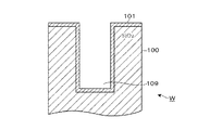
本発明の実施の形態に係る半導体装置の製造方法に使用される半導体装置製造用の基板であるウエハWの表面構造の一例について説明する。図1は半導体装置の製造工程の途中段階におけるウエハWの表面構造を示す。この表面構造は第1の層に相当するシリコン酸化膜(SiO2膜)100がエッチングされて凹部であるホール109が形成されている。そしてホール109の内側を含むSiO2膜100の表面が窒化されて、第2の層に相当する窒化シリコン膜からなるバリア膜101が形成されている。窒化シリコン膜は、理論的には、Si3N4で表わされるが、本願明細書では、「SiN膜」と略記する。
An example of the surface structure of a wafer W that is a substrate for manufacturing a semiconductor device used in the method for manufacturing a semiconductor device according to an embodiment of the present invention will be described. FIG. 1 shows the surface structure of the wafer W in the middle of the semiconductor device manufacturing process. In this surface structure, a silicon oxide film (SiO 2 film) 100 corresponding to the first layer is etched to form a
その後、ウエハWに向けて、例えばCF4ガスを供給することで、バリア膜101がドライエッチングされる。これにより図2に示すようにウエハWの表面及びホール109の底面に形成されたバリア膜101が除去されて、SiO2膜100が露出する。この時、ホール109の側面に形成されたバリア膜101は除去されずに残る。こうして形成されたコンタクトホールのアスペクト比(深さ/孔径)は、例えば1〜50である。
Thereafter, the
続いてウエハWを例えばALDにより成膜する成膜装置に搬入し、ウエハWの表面にSiN膜を成膜する前段工程である1回目の成膜工程を行う。成膜装置においては、例えばウエハWに向けて、シリコンを含むガス、例えばDCS(ジクロロシラン)と、NH3ガスをプラズマ化して得たプラズマ(アンモニアプラズマ)と、を交互に複数回供給する。これによりウエハWの表面にDCSが吸着し、次いでDCSとアンモニアプラズマとが反応してSiNの分子層が形成され、この分子層が順次積層されてSiN膜が成膜される。 Subsequently, the wafer W is loaded into a film forming apparatus for forming a film by ALD, for example, and a first film forming process, which is a pre-process for forming a SiN film on the surface of the wafer W, is performed. In the film forming apparatus, for example, a gas containing silicon, for example, DCS (dichlorosilane) and plasma (ammonia plasma) obtained by converting NH 3 gas into plasma are alternately supplied to the wafer W a plurality of times. As a result, DCS is adsorbed on the surface of the wafer W, and then DCS and ammonia plasma react to form a SiN molecular layer, and this molecular layer is sequentially laminated to form a SiN film.
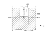
しかしながらホール109が細くかつ深い構造の場合、即ちホール109のアスペクト比が大きい場合、ホール109を隙間なく埋め切る前にSiN膜102がホール109の上方を閉塞し、図3に示すようにホール109を埋めるSiN膜102にボイドやシームなどの隙間が形成されることがある。
However, when the
続いて1回目の成膜工程を行ったウエハWは、成膜装置から搬出され、例えば公知のウェットエッチングを行う液処理装置に搬入される。液処理装置に搬入されたウエハWは、例えば160〜165℃に加熱されたリン酸液に浸漬される。エッチング処理の手法としては、スピンチャックにウエハWを吸着させて回転させながら上方のノズルからエッチング液をウエハWに供給する手法、あるいはエッチング層に複数枚のウエハWを一括して浸漬する手法などが挙げられる。そしてエッチング停止のタイミングとしては、SiN膜102の上面がホール109の開口面よりも低くなり、かつ空隙(例えばボイド)が露出している状態になるタイミングを上げることができる。
Subsequently, the wafer W that has undergone the first film formation step is unloaded from the film forming apparatus and is loaded into, for example, a known liquid processing apparatus that performs wet etching. The wafer W carried into the liquid processing apparatus is immersed in, for example, a phosphoric acid solution heated to 160 to 165 ° C. Etching methods include a method of supplying an etching solution to the wafer W from an upper nozzle while adsorbing and rotating the wafer W on a spin chuck, or a method of immersing a plurality of wafers W in an etching layer at once. Is mentioned. Etching can be stopped at a timing when the upper surface of the SiN
このように空隙が露出しているタイミングでエッチングを止めれば、後述の第2回目以降の成膜時に空隙が埋められ、空隙がなくなるまでエッチングする場合に比べてエッチング時間及び次工程の成膜時間が短くて済み処理効率が良い。図4はエッチング処理後のウエハWの表面の状態を示し、ウエハW表面のSiO2膜100が露出していると共に、ホール109に埋め込まれたSiN膜102の表面側の部分が除去されている。
If the etching is stopped at the timing when the gap is exposed in this way, the etching time and the film formation time of the next process are compared with the case where the gap is filled during the second and subsequent film formation described later and etching is performed until the gap disappears. Is short and processing efficiency is good. FIG. 4 shows the state of the surface of the wafer W after the etching process. The SiO 2
エッチング工程を行ったウエハWは、液処理装置から搬出され、例えば1回目の成膜工程に用いた成膜装置に搬入される。そしてSiN膜を成膜する2回目の成膜工程を行う。2回目の成膜工程においても、1回目の成膜工程と同様にDCSと、NH3ガスをプラズマ化して得たプラズマ(アンモニアプラズマ)と、を交互に複数回供給する。 The wafer W that has been subjected to the etching process is unloaded from the liquid processing apparatus, and is loaded into the film forming apparatus used in the first film forming process, for example. Then, a second film forming process for forming the SiN film is performed. Also in the second film formation step, DCS and plasma (ammonia plasma) obtained by converting NH 3 gas into plasma are alternately supplied a plurality of times as in the first film formation step.
既述のエッチング工程後のウエハWの表面においてSiO2膜100の表面が露出しているので、SiN膜が成膜される被成膜領域は、SiO2膜100の表面、バリア膜(SiN膜)101及びホール109に埋め込まれたSiN膜102の表面である。これらの表面におけるSiNの成膜に係るインキュベーションタイムは、SiO2膜100の方がバリア膜101及びSiN膜102よりも長い。インキュベーションタイムとは、成膜用の処理ガスを被処理表面に供給した時点から、薄膜の成膜が開始されるまでの時間である。インキュベーションタイムが発生する理由は、被処理表面と成膜種との関係において、膜の成長が起こる核が被処理表面に形成されることが必要な場合があり、処理ガスを被処理表面に供給した後、核の形成に時間を要することが挙げられる。
Since the surface of the SiO 2
SiO2膜100の表面においては、SiNの分子層が積層され始めるために必要な核が処理ガスの供給と同時に形成されるのではなく、少し遅れて形成される。一方、バリア膜101と成膜すべき膜(SiN膜103)とは、化合物という観点では同種であることから、バリア膜101の表面には処理ガスの供給とほぼ同時にSiN膜103の成膜が行われる。バリア膜101及びSiN膜102の表面は成膜が進んでいるが、SiO2膜100の表面はまだ成膜が開始されていない様子を図5に模式的に示す。なお、図5ではバリア膜101及びSiN膜102上の成膜が進んでいる状態を強調して描いている。従って処理ガスを供給した後のあるタイミングでSiN膜103の膜厚を見ると、SiO2膜100の表面よりもホール109の内周面における膜厚の方が厚い。
On the surface of the SiO 2 film 100, the nuclei necessary for the SiN molecular layer to begin to be stacked are not formed at the same time as the processing gas is supplied, but are formed with a slight delay. On the other hand, since the
従って、図5に示した状態からさらに成膜を行った時に図6に示すようにSiO2膜100の表面側に形成されるホール109の上方の周囲から押し寄せるSiN膜103が、ホール109の上方を閉塞させる前に、ホール109の内部にSiN膜103を隙間なく埋めきることができる。
その後ウエハWは、例えばCMP(Chemical Mechanical Polishing)により研磨されて、SiO2膜100の表面のSiN膜103が除去される。これにより図7に示すようにウエハWの表面にSiO2膜100が露出し、ホール109がSiN膜103(102)により埋め込まれた状態となる。
Accordingly, when further film formation is performed from the state shown in FIG. 5, the
Thereafter, the wafer W is polished by, for example, CMP (Chemical Mechanical Polishing), and the
ウエハWにSiN膜102、103を成膜する成膜装置の一例を挙げておく。成膜装置10は、図8〜図9に示すように、扁平な円筒状の真空容器11と、真空容器11内に設けられ、周方向に沿って例えば5枚のウエハWを載置する回転テーブル12と、を備えている。回転テーブル12には、回転機構13が設けられ、回転テーブル12は、鉛直軸周りに回転する。真空容器11における回転テーブル12のウエハWの載置部分の下方には、回転テーブルに載置されたウエハWを加熱するヒータ15が設けられている。真空容器11には、回転テーブル12の回転方向に沿って、原料ガス供給領域R1及び窒化ガス供給領域R2が設けられている。
An example of a film forming apparatus for forming the
原料ガス供給領域R1における回転テーブル12の上方は、ガス給排気部3が設けられている。ガス給排気部3における、中心側の領域はガスシャワーヘッド31となっている。ガスシャワーヘッド31は、例えば下方に向けて原料ガスであるDCSガスを供給できるように構成されており、回転テーブル12に載置されたウエハWが原料ガス供給領域R1に位置すると、DCSガスが当該ウエハWの表面に供給されて吸着される。またガス給排気部3の下面には、その周縁に沿って、環状の分離ガス吐出口32が開口しており、さらに分離ガス吐出口32と、ガスシャワーヘッド31との間には、分離ガス吐出口32に沿って環状の排気口33が設けられている。分離ガス吐出口32は、原料ガス供給領域R1の下方の周縁部に分離ガスであるアルゴン(Ar)ガスを供給するように構成されている。また排気口33は、ガスシャワーヘッド31からウエハWに向けて供給されたDCSガスを排気すると共に、分離ガスを吸引して排気する。この排気口33によるDCSガスの排気と、分離ガス吐出口32から分離ガスを吐出して、排気口33に向かう流れを形成することにより、DCSガスが原料ガス供給領域R1の外へ流れないようになっている。なお図9中の34はDCSガス供給源、35は分離ガス供給源、36は排気手段である。
A gas supply / exhaust unit 3 is provided above the
窒化ガス供給領域R2は、例えば2本のガスノズル41からガスノズル41挟まれた窒化ガス供給領域R2にNH3ガスを供給すると共に、窒化ガス供給領域R2上方からマイクロ波を供給するように構成されている。なお図8中の40はガス供給管、42はNH3ガス供給源、44は流量調整部を示す。また図9中の21は誘電体窓、22は誘電体プレート、23は導波管、24はマイクロ波供給部を示す。そして窒化ガス供給領域R2にNH3ガスを供給した後、マイクロ波が供給されてNH3ガスがプラズマ化する。そして回転テーブル12が回転し表面にDCSが吸着したウエハWが窒化ガス供給領域R2に進入すると、ウエハW表面に吸着したDCSとアンモニアプラズマとが反応してSiNの分子層が形成される。このようにウエハWを載置した回転テーブル12を回転させることにより、ウエハWが各領域を交互に通過することにより、原料ガスの吸着、吸着した原料ガスの窒化が繰り返されてSiN層が積層されていく。
For example, the nitriding gas supply region R2 is configured to supply NH 3 gas from two
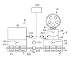
続いて本発明の半導体装置の製造方法を実施する半導体装置の製造システムである基板処理システムの一例を示す。図10に示すように基板処理システムは、ウエハWにSiN膜を成膜するための真空処理システム9を備えている。真空処理システム9は、既述の成膜装置10を備え、ウエハWを収納したキャリアCが載置されるキャリア載置部91を備えており、キャリア載置部91に載置されたキャリアCから取り出されたウエハWは、常圧搬送室92、ロードロック室93及び真空搬送室94を介して成膜装置10に搬入される。なお図10中の95、及び96は夫々常圧搬送室92及び真空搬送室94に設けられた搬送アームであり、97は、ゲートバルブである。
Next, an example of a substrate processing system, which is a semiconductor device manufacturing system for performing the semiconductor device manufacturing method of the present invention, will be described. As shown in FIG. 10, the substrate processing system includes a vacuum processing system 9 for forming a SiN film on the wafer W. The vacuum processing system 9 includes the
また基板処理システムは、ウエハWに成膜されたSiN膜をエッチングする液処理システム8を備えている。液処理システム8は、キャリア載置部81と、搬送アーム83を備えた受け渡し部82と、液処理部84と、を備えている。液処理部84は、例えばウエハWを、エッチング液である加熱されたリン酸の貯留された液槽に浸漬してSiN膜102をエッチングするエッチング部、ウエハWに付着したリン酸を洗浄する洗浄部などを備えている。キャリア載置部81において、キャリアCから取り出されたウエハWは、搬送アーム83を介して液処理部84に受け渡され、液処理後にキャリアCに戻される。
The substrate processing system also includes a liquid processing system 8 that etches the SiN film formed on the wafer W. The liquid processing system 8 includes a
また基板処理システムは、例えば天井搬送機構300を備えている。天井搬送機構300は、天井に沿って配置されたガイドレール301とキャリアCを搬送する搬送部302とを備えている。
さらに基板処理システムは、液処理システム8、真空処理システム9及び天井搬送機構300を各々制御するコントローラ202、203及び204を備えており、各コントローラ202、203及び204は、上位制御部である上位コンピュータ200により指示される。上位コンピュータ200は、例えば図2に示すウエハWに対して、真空処理システム9にて、1回目のSiN膜102の成膜処理を行う工程、次いで液処理システム8にて、SiN膜102膜のエッチング処理を行う工程、その後真空処理システム9に戻し、2回目のSiN膜103の成膜処理を行う工程を順次実施するためのプログラムを備えている。
Further, the substrate processing system includes a
The substrate processing system further includes
上述の実施形態では、SiO2膜100に形成された凹部109に対して、例えばALDによりSiN膜102の成膜を行って埋め込みを行った後、例えばウェットエッチングによりSiN膜102を、ウエハW表面のSiO2膜100が露出するまでエッチングした後、再度SiN膜103の埋め込み処理(成膜処理)を行っている。既に詳述したように、SiN膜103の成膜に係るインキュベーションタイム(処理ガス供給時から成膜開始までの遅れ時間)は、SiO2膜100の方がバリア膜101よりも長い。このため、エッチング後の再度のSiN膜103の埋め込み処理においては、SiO2膜100の上面側から凹部109の上方にSiN膜103が押し寄せる前に凹部109内にSiN膜103が埋め込まれるので、ボイドやシームなどの空隙の発生を抑えることができる。
In the above-described embodiment, the
また上述の実施の形態においては、エッチング工程と、その後の成膜工程とを1回ずつ行っているが、例えばホール109のアスペクト比がかなり大きいなどの事情により各工程が一回の場合には、空隙が生じるおそれがある場合には、2回目の成膜工程を行った後、エッチング工程と、その後の成膜工程と、を1回以上繰り返してもよい。
In the above-described embodiment, the etching process and the subsequent film formation process are performed once. However, when each process is performed once due to, for example, the aspect ratio of the
さらに半導体装置製造用の基板の他の例について説明する。図11に示すように例えば1回目の成膜処理を行う前のウエハWとして、第1の層となるSiO2膜100が第2の層となるシリコン層104の表面に成膜され、SiO2膜100からシリコン層104まで貫通するようにホール109が形成された構成が挙げられる。このようなウエハWにおいては、ホール109における大部分の側面は、シリコンとなっている。そのため例えばSiNによりホールを埋めるように成膜する場合には、シリコンとSiO2とのインキュベーションタイムの差を利用してホール109にSiNを埋め込むことができるため、本発明を適用することができる
Further, another example of a substrate for manufacturing a semiconductor device will be described. As shown in FIG. 11, for example, as a wafer W before the first film formation process, a SiO 2 film 100 as a first layer is formed on the surface of a
またホール109の内面を除くウエハWの表面のバリア膜101を除去して、ウエハW表面のSiO2膜100を露出させるにあたっては、CMPを用いてもよい。CMPの場合には、ウエハWの表面を研磨により除去するため図12に示すようにホール109の内側の底面のバリア膜101も残すことができる。そのため続いて1回目の成膜工程においてSiN膜102を成膜したときにホール109の内部の底面おいて、バリア膜101に積層されるためSiNの膜厚が速やかに厚くなる。ボイドやシームなどの空隙は、ホール109の側面から成長するSiN膜同士の間に形成されるため、ホール109の底面から積層されるSiN膜の厚さが厚くなると、空隙がホール109の深い位置に形成されにくくなる。そのためエッチング工程にてホール109を埋めたSiN膜102のエッチングを少なくすることができる。
CMP may be used to remove the
またSiN膜102をエッチングするエッチング工程は、例えばCF4、NF3、CH2F2、C4F8、C4F6、C3F8及びCHF3などのガスを用いたドライエッチングにより行ってもよく、この場合には、図10の真空処理システム9の真空搬送室94にドライエッチングを行うエッチングモジュール(真空容器内にドライエッチングを行うための設備、機器を設けたモジュール)を接続してもよい。このような真空処理システム9によれば、成膜装置10とエッチングモジュール(エッチング装置)との間において、真空搬送室94の搬送アーム96がウエハWの受け渡しを行うので成膜→エッチング→成膜を行った後、さらにエッチング→成膜を1回以上行う場合であっても高いスループットで実施することができる。
さらに成膜装置は、例えば1枚のウエハWを真空容器内に載置して処理を行う枚葉式の成膜装置でも良い。あるいはウエハWに原料ガスと、反応ガスとを供給して、ウエハWの表面に分子層(あるいは原子層)を積層するCVD(chemical vapor deposition)法を行う成膜装置でもよい。
The etching process for etching the
Furthermore, the film forming apparatus may be, for example, a single wafer type film forming apparatus that performs processing by placing one wafer W in a vacuum vessel. Alternatively, a film forming apparatus that supplies a source gas and a reactive gas to the wafer W and performs a chemical vapor deposition (CVD) method in which a molecular layer (or an atomic layer) is stacked on the surface of the wafer W may be used.
8 液処理システム
9 真空処理システム
10 成膜装置
100 SiO2膜
101 バリア膜
102 1回目のSiN膜
103 2回目のSiN膜
109 溝部
200 上位コンピュータ
202〜204 コンピュータ
300 天井搬送機構
W ウエハ
8 Liquid processing system 9
Claims (4)
次に前記第3の層をエッチングし、前記第1の層の上面が露出すると共に凹部内に第3の層が残った状態でエッチングを停止するエッチング工程と、
その後、基板の上に処理ガスを供給して第3の層を形成し、当該第3の層により前記凹部を埋め込む後段工程と、を含み、
前記第1の層はシリコン酸化層であり、前記第2の層は窒化シリコン層であり、前記第3の層は窒化シリコン層であることと、
前記処理ガスを供給した時に、第1の層の表面におけるインキュベーションタイムが第2の層の表面におけるインキュベーションタイムよりも長いことと、を特徴とする半導体装置の製造方法。 The surface of the first layer is exposed on the upper surface, and a recess is formed in the first layer, and a processing gas is applied onto the substrate for manufacturing a semiconductor device in which the side wall of the recess is covered with the second layer. A pre-process for supplying to form a third layer and filling the recess with the third layer;
Next, etching the third layer to stop the etching with the top surface of the first layer exposed and the third layer remaining in the recess; and
Thereafter, a process gas is supplied onto the substrate to form a third layer, and the recessed step is embedded in the third layer.
The first layer is a silicon oxide layer, the second layer is a silicon nitride layer, and the third layer is a silicon nitride layer;
When supplying the processing gas, a method of manufacturing a semiconductor device incubation time at the surface of the first layer and wherein the long and than incubation time at the surface of the second layer.
Priority Applications (4)
| Application Number | Priority Date | Filing Date | Title |
|---|---|---|---|
| JP2016057341A JP6583081B2 (en) | 2016-03-22 | 2016-03-22 | Manufacturing method of semiconductor device |
| TW106108647A TWI662607B (en) | 2016-03-22 | 2017-03-16 | Semiconductor device manufacturing method and semiconductor device manufacturing system |
| KR1020170033034A KR102103625B1 (en) | 2016-03-22 | 2017-03-16 | Semiconductor device manufacturing method and semiconductor device manufacturing system |
| US15/465,144 US10297443B2 (en) | 2016-03-22 | 2017-03-21 | Semiconductor device manufacturing method and semiconductor device manufacturing system |
Applications Claiming Priority (1)
| Application Number | Priority Date | Filing Date | Title |
|---|---|---|---|
| JP2016057341A JP6583081B2 (en) | 2016-03-22 | 2016-03-22 | Manufacturing method of semiconductor device |
Publications (3)
| Publication Number | Publication Date |
|---|---|
| JP2017174902A JP2017174902A (en) | 2017-09-28 |
| JP2017174902A5 JP2017174902A5 (en) | 2018-12-13 |
| JP6583081B2 true JP6583081B2 (en) | 2019-10-02 |
Family
ID=59896679
Family Applications (1)
| Application Number | Title | Priority Date | Filing Date |
|---|---|---|---|
| JP2016057341A Active JP6583081B2 (en) | 2016-03-22 | 2016-03-22 | Manufacturing method of semiconductor device |
Country Status (4)
| Country | Link |
|---|---|
| US (1) | US10297443B2 (en) |
| JP (1) | JP6583081B2 (en) |
| KR (1) | KR102103625B1 (en) |
| TW (1) | TWI662607B (en) |
Families Citing this family (7)
| Publication number | Priority date | Publication date | Assignee | Title |
|---|---|---|---|---|
| US11056348B2 (en) | 2018-04-05 | 2021-07-06 | Invensas Bonding Technologies, Inc. | Bonding surfaces for microelectronics |
| JP7040257B2 (en) * | 2018-04-25 | 2022-03-23 | 東京エレクトロン株式会社 | Film forming equipment and film forming method |
| JP7004608B2 (en) * | 2018-05-11 | 2022-01-21 | 東京エレクトロン株式会社 | Semiconductor film forming method and film forming equipment |
| US10741442B2 (en) | 2018-05-31 | 2020-08-11 | Taiwan Semiconductor Manufacturing Company, Ltd. | Barrier layer formation for conductive feature |
| US10872788B2 (en) * | 2018-11-26 | 2020-12-22 | Taiwan Semiconductor Manufacturing Co., Ltd. | Wet etch apparatus and method for using the same |
| CN110459464B (en) * | 2019-08-14 | 2021-09-14 | 中国科学院微电子研究所 | Preparation method of thick film silicon nitride by regional grooving |
| US11264357B1 (en) | 2020-10-20 | 2022-03-01 | Invensas Corporation | Mixed exposure for large die |
Family Cites Families (21)
| Publication number | Priority date | Publication date | Assignee | Title |
|---|---|---|---|---|
| JPS5654049A (en) * | 1979-10-09 | 1981-05-13 | Mitsubishi Electric Corp | Semiconductor device |
| JP2812599B2 (en) * | 1992-02-06 | 1998-10-22 | シャープ株式会社 | Method for manufacturing semiconductor device |
| JPH07297182A (en) * | 1994-04-27 | 1995-11-10 | Sony Corp | Method of forming sin-based insulating film |
| JP3660391B2 (en) * | 1994-05-27 | 2005-06-15 | 株式会社東芝 | Manufacturing method of semiconductor device |
| US20010028922A1 (en) * | 1995-06-07 | 2001-10-11 | Sandhu Gurtej S. | High throughput ILD fill process for high aspect ratio gap fill |
| JP3402972B2 (en) | 1996-11-14 | 2003-05-06 | 東京エレクトロン株式会社 | Method for manufacturing semiconductor device |
| US7115516B2 (en) * | 2001-10-09 | 2006-10-03 | Applied Materials, Inc. | Method of depositing a material layer |
| JP2003243537A (en) * | 2002-02-18 | 2003-08-29 | Mitsubishi Electric Corp | Semiconductor device and manufacturing method thereof |
| JP3759525B2 (en) * | 2003-10-27 | 2006-03-29 | 松下電器産業株式会社 | Manufacturing method of semiconductor device |
| WO2005062390A1 (en) * | 2003-12-22 | 2005-07-07 | Showa Denko K.K. | Group iii nitride semiconductor device and light-emitting device using the same |
| US7482247B1 (en) * | 2004-12-30 | 2009-01-27 | Novellus Systems, Inc. | Conformal nanolaminate dielectric deposition and etch bag gap fill process |
| KR100711928B1 (en) * | 2005-12-29 | 2007-04-27 | 동부일렉트로닉스 주식회사 | Metal line in semiconductor and fabricating method thereof |
| JP5550843B2 (en) * | 2009-03-19 | 2014-07-16 | ラピスセミコンダクタ株式会社 | Manufacturing method of semiconductor device |
| US8742476B1 (en) * | 2012-11-27 | 2014-06-03 | Monolithic 3D Inc. | Semiconductor device and structure |
| JP5490753B2 (en) * | 2010-07-29 | 2014-05-14 | 東京エレクトロン株式会社 | Trench filling method and film forming system |
| JP5544343B2 (en) * | 2010-10-29 | 2014-07-09 | 東京エレクトロン株式会社 | Deposition equipment |
| JP5599350B2 (en) * | 2011-03-29 | 2014-10-01 | 東京エレクトロン株式会社 | Film forming apparatus and film forming method |
| JP5829926B2 (en) * | 2011-07-06 | 2015-12-09 | 東京エレクトロン株式会社 | Method for forming tungsten film |
| JP5162016B1 (en) * | 2011-09-15 | 2013-03-13 | 株式会社東芝 | Semiconductor device, wafer, semiconductor device manufacturing method, and wafer manufacturing method |
| US9000557B2 (en) * | 2012-03-17 | 2015-04-07 | Zvi Or-Bach | Semiconductor device and structure |
| JP6468955B2 (en) * | 2015-06-23 | 2019-02-13 | 東京エレクトロン株式会社 | Method and apparatus for forming silicon-containing film |
-
2016
- 2016-03-22 JP JP2016057341A patent/JP6583081B2/en active Active
-
2017
- 2017-03-16 KR KR1020170033034A patent/KR102103625B1/en active IP Right Grant
- 2017-03-16 TW TW106108647A patent/TWI662607B/en active
- 2017-03-21 US US15/465,144 patent/US10297443B2/en active Active
Also Published As
| Publication number | Publication date |
|---|---|
| KR20170110020A (en) | 2017-10-10 |
| TW201738947A (en) | 2017-11-01 |
| US10297443B2 (en) | 2019-05-21 |
| JP2017174902A (en) | 2017-09-28 |
| US20170278698A1 (en) | 2017-09-28 |
| KR102103625B1 (en) | 2020-04-22 |
| TWI662607B (en) | 2019-06-11 |
Similar Documents
| Publication | Publication Date | Title |
|---|---|---|
| JP6583081B2 (en) | Manufacturing method of semiconductor device | |
| JP7190814B2 (en) | Air gap formation method | |
| TWI828989B (en) | Tin oxide films in semiconductor device manufacturing | |
| TWI657535B (en) | Selective formation of dielectric barriers for metal interconnects in semiconductor devices | |
| TWI493654B (en) | Apparatus, method for depositing thin film on wafer and method for gap-filling trench using the same | |
| KR102345587B1 (en) | Sacrificial pre-metal dielectric for self-aligned contact scheme | |
| KR102216529B1 (en) | Manufacturing method for semiconductor device | |
| JP2020529736A (en) | Selective deposition of SiN on a horizontal surface | |
| KR20170018817A (en) | Substrate processing system and substrate processing method | |
| KR102441239B1 (en) | Etching method | |
| KR102297695B1 (en) | Densification of dielectric film using inductively coupled high density plasma | |
| TW201726963A (en) | Methods for formation of low-k aluminum-containing etch stop films | |
| JP7208318B2 (en) | processing equipment | |
| KR20210134737A (en) | Film-forming method and film-forming apparatus | |
| CN111719137B (en) | Method for cleaning film forming apparatus | |
| CN112442680A (en) | Film forming apparatus and film forming method | |
| TW202105490A (en) | Etch stop layer | |
| US20220389571A1 (en) | Apparatus For Single Chamber Deposition And Etch | |
| TW202314800A (en) | Methods and apparatus for selective etch stop capping and selective via open for fully landed via on underlying metal |
Legal Events
| Date | Code | Title | Description |
|---|---|---|---|
| RD02 | Notification of acceptance of power of attorney |
Free format text: JAPANESE INTERMEDIATE CODE: A7422 Effective date: 20180117 |
|
| A621 | Written request for application examination |
Free format text: JAPANESE INTERMEDIATE CODE: A621 Effective date: 20180824 |
|
| A521 | Request for written amendment filed |
Free format text: JAPANESE INTERMEDIATE CODE: A523 Effective date: 20180918 |
|
| A521 | Request for written amendment filed |
Free format text: JAPANESE INTERMEDIATE CODE: A523 Effective date: 20181030 |
|
| A977 | Report on retrieval |
Free format text: JAPANESE INTERMEDIATE CODE: A971007 Effective date: 20190510 |
|
| A131 | Notification of reasons for refusal |
Free format text: JAPANESE INTERMEDIATE CODE: A131 Effective date: 20190521 |
|
| A521 | Request for written amendment filed |
Free format text: JAPANESE INTERMEDIATE CODE: A523 Effective date: 20190719 |
|
| TRDD | Decision of grant or rejection written | ||
| A01 | Written decision to grant a patent or to grant a registration (utility model) |
Free format text: JAPANESE INTERMEDIATE CODE: A01 Effective date: 20190806 |
|
| A61 | First payment of annual fees (during grant procedure) |
Free format text: JAPANESE INTERMEDIATE CODE: A61 Effective date: 20190819 |
|
| R150 | Certificate of patent or registration of utility model |
Ref document number: 6583081 Country of ref document: JP Free format text: JAPANESE INTERMEDIATE CODE: R150 |
|
| R250 | Receipt of annual fees |
Free format text: JAPANESE INTERMEDIATE CODE: R250 |
|
| R250 | Receipt of annual fees |
Free format text: JAPANESE INTERMEDIATE CODE: R250 |