JP6576216B2 - Processing device, inspection device, and positional deviation amount specifying method - Google Patents
Processing device, inspection device, and positional deviation amount specifying method Download PDFInfo
- Publication number
- JP6576216B2 JP6576216B2 JP2015220013A JP2015220013A JP6576216B2 JP 6576216 B2 JP6576216 B2 JP 6576216B2 JP 2015220013 A JP2015220013 A JP 2015220013A JP 2015220013 A JP2015220013 A JP 2015220013A JP 6576216 B2 JP6576216 B2 JP 6576216B2
- Authority
- JP
- Japan
- Prior art keywords
- probing
- probe
- processing
- dent
- image
- Prior art date
- Legal status (The legal status is an assumption and is not a legal conclusion. Google has not performed a legal analysis and makes no representation as to the accuracy of the status listed.)
- Active
Links
Images


Landscapes
- Measuring Leads Or Probes (AREA)
- Tests Of Electronic Circuits (AREA)
Description
本発明は、プロービング対象の被接触面における規定位置とプロービングによってプローブの先端部が実際に位置するプロービング位置との位置ずれ量を特定する処理装置、その処理装置を備えた検査装置、および規定位置とプロービング位置との位置ずれ量を特定する位置ずれ量特定方法に関するものである。 The present invention relates to a processing device that specifies a positional deviation amount between a specified position on a contacted surface to be probed and a probing position where the tip of the probe is actually positioned by probing, an inspection device including the processing device, and a specified position. The present invention relates to a positional deviation amount specifying method for specifying a positional deviation amount between a probing position and a probing position.
この種の基板検査装置として、下記特許文献1において出願人が開示したX−Y回路基板検査装置が知られている。このX−Y回路基板検査装置は、移動機構によってX−Y方向にプローブを移動させて回路基板の表面にプローブをプロービングさせ、プローブを介して入出力する電気信号に基づいて回路基板を検査することが可能に構成されている。また、このX−Y回路基板検査装置は、専用ボード、カメラおよび画像処理手段を備え、プローブの取り付け誤差を特定することが可能に構成されている。この場合、カメラはプローブと共に移動機構によって移動させられる。このX−Y回路基板検査装置では、プローブの取り付け誤差を特定する際には、まず、カメラの取付け誤差の吸収(調整)を行う。具体的には、カメラを専用ボードのマークの上に移動させてマークを撮像させ、次いで、画像処理手段が画像からマークの重心(図心)を求める。続いて、カメラの中心とマークの重心とを位置合わせする。これにより、カメラの取り付け誤差が吸収される。次いで、プローブの取り付け誤差を特定する。具体的には、専用ボードの打痕シート上における特定点(特定点の座標を(x,y)とする)を指定して移動機構にプロービングを指示する。続いて、カメラを特定点の上に移動させて打痕シートに生じた打痕を撮像させ、次いで、画像処理手段が画像から打痕の重心を求める。続いて、重心の座標と特定点の座標との差を取り付け誤差として求める。回路基板の検査を行う際に、このようにして求めた取り付け誤差を用いて、回路基板の表面にプローブをプロービングさせる際のプローブの移動量を補正することで、プロービング位置にプローブを正確にプロービングさせることが可能となる。 As this type of board inspection apparatus, an XY circuit board inspection apparatus disclosed by the applicant in Patent Document 1 below is known. In this XY circuit board inspection apparatus, a probe is moved in the XY direction by a moving mechanism to probe the probe on the surface of the circuit board, and the circuit board is inspected based on an electrical signal input / output via the probe. It is configured to be possible. The XY circuit board inspection apparatus includes a dedicated board, a camera, and image processing means, and is configured to be able to specify a probe mounting error. In this case, the camera is moved by the moving mechanism together with the probe. In this XY circuit board inspection apparatus, when specifying the probe mounting error, first, the camera mounting error is absorbed (adjusted). Specifically, the camera is moved over the mark on the dedicated board to image the mark, and then the image processing means obtains the center of gravity (centroid) of the mark from the image. Subsequently, the center of the camera and the center of gravity of the mark are aligned. As a result, camera mounting errors are absorbed. Next, the probe mounting error is specified. Specifically, a specific point on the dent sheet of the dedicated board (designating the coordinate of the specific point as (x, y)) is specified and the moving mechanism is instructed to perform probing. Subsequently, the camera is moved over a specific point to image the dent formed on the dent sheet, and then the image processing means obtains the center of gravity of the dent from the image. Subsequently, the difference between the coordinates of the center of gravity and the coordinates of the specific point is obtained as an attachment error. When inspecting a circuit board, the probe is accurately probed at the probing position by correcting the amount of movement of the probe when probing the probe on the surface of the circuit board using the mounting error obtained in this way. It becomes possible to make it.
ところが、上記のX−Y回路基板検査装置には、改善すべき以下の課題がある。すなわち、このX−Y回路基板検査装置では、打痕シートにプローブをプロービングさせて生じさせた打痕を撮像することで、プローブの取り付け誤差を特定している。一方、回路基板の高密度化に伴ってプローブも小形化(小径化)しているため、プローブによって生じる打痕が小さくなっている。この場合、打痕が小さいときには、撮像した画像における打痕の形状が不明瞭となり、打痕の重心を正確に求めることが困難となる。したがって、上記のX−Y回路基板検査装置には、小形のプローブを用いる場合において、そのプローブの取り付け誤差を正確に求めることが困難となるおそれがある。 However, the above XY circuit board inspection apparatus has the following problems to be improved. That is, in this XY circuit board inspection apparatus, an attachment error of the probe is specified by imaging a dent produced by probing the probe on the dent sheet. On the other hand, as the density of the circuit board increases, the probe also becomes smaller (smaller in diameter), so that the dent produced by the probe is smaller. In this case, when the dent is small, the shape of the dent in the captured image becomes unclear, and it is difficult to accurately obtain the center of gravity of the dent. Therefore, in the above-described XY circuit board inspection apparatus, when a small probe is used, it may be difficult to accurately obtain an attachment error of the probe.
本発明は、かかる改善すべき課題に鑑みてなされたものであり、小形のプローブを用いる場合においても、プロービング位置と規定位置との位置ずれ量を正確に特定し得る処理装置、検査装置および位置ずれ量特定方法を提供することを主目的とする。 The present invention has been made in view of such a problem to be improved, and in the case of using a small probe, a processing apparatus, an inspection apparatus, and a position that can accurately specify the amount of positional deviation between the probing position and the specified position. The main purpose is to provide a method for specifying the amount of deviation.
上記目的を達成すべく請求項1記載の処理装置は、プロービング機構にプローブのプロービングを実行させて保持位置に保持されたプロービング対象の被接触面における規定位置に対して当該プローブの先端部を接触させる際の当該先端部が実際に位置するプロービング位置と当該規定位置との位置ずれ量を特定する特定処理を実行する処理装置であって、前記保持位置に保持された前記プロービング対象の前記被接触面を撮像する撮像部と、前記保持位置に保持させた前記プロービング対象としての打痕シートの前記被接触面における前記規定位置に対して前記プロービング機構に前記プロービングを実行させたときに生じる打痕の前記撮像部によって撮像された画像を用いて前記特定処理を実行する処理部とを備え、前記処理部は、前記特定処理において、前記画像を画像処理することによって前記打痕の形状の図心の位置を算出する算出処理を複数回実行し、前記各算出処理によって算出した複数の図心の位置を統計処理して求めた処理位置を前記プロービング位置として前記位置ずれ量を特定する。 In order to achieve the above object, the processing apparatus according to claim 1, wherein the probing mechanism performs probe probing to contact the tip of the probe with a predetermined position on the contacted surface of the probing target held at the holding position. A processing device that executes a specific process for specifying a positional deviation amount between a probing position where the tip portion is actually positioned and the specified position when the tip is touched, and the contacted target of the probing object held at the holding position An imaging unit that images a surface, and a dent generated when the probing mechanism performs the probing on the specified position on the contacted surface of the dent sheet as the probing target held at the holding position And a processing unit that executes the specific process using an image captured by the imaging unit. In the fixed process, a calculation process for calculating the position of the centroid of the shape of the impression by performing image processing on the image is performed a plurality of times, and statistical processing is performed on the positions of the plurality of centroids calculated by the calculation processes. The positional deviation amount is specified using the processing position obtained in this way as the probing position.
また、請求項2記載の処理装置は、請求項1記載の処理装置において、前記処理部は、前記統計処理として前記複数の図心の位置を示す座標を相加平均して前記処理位置を求める。
The processing device according to
また、請求項3記載の処理装置は、請求項1または2記載の処理装置において、前記処理部は、前記画像処理において、前記画像を構成する画素の中から前記打痕を構成する画素を抽出し、当該抽出した画素の外周で規定される形状を前記打痕の形状として前記図心の位置を算出する。
The processing device according to
また、請求項4記載の検査装置は、請求項1から3のいずれかに記載の処理装置と、前記プロービング機構と、当該プロービング機構を制御する制御部と、前記プローブを介して入出力する電気信号に基づいて物理量を測定する測定部と、当該測定部によって測定された前記物理量に基づいて前記プロービング対象を検査する検査部とを備えている。 According to a fourth aspect of the present invention, there is provided an inspection apparatus according to any one of the first to third aspects, the probing mechanism, a control unit that controls the probing mechanism, and an electric input / output via the probe. A measurement unit that measures a physical quantity based on the signal; and an inspection unit that inspects the probing target based on the physical quantity measured by the measurement unit.
また、請求項5記載の位置ずれ量特定方法は、プロービング機構にプローブのプロービングを実行させて保持位置に保持されたプロービング対象の被接触面における規定位置に対して当該プローブの先端部を接触させる際の当該先端部が実際に位置するプロービング位置と当該規定位置との位置ずれ量を特定する位置ずれ量特定方法であって、前記保持位置に保持させた前記プロービング対象としての打痕シートの前記被接触面における前記規定位置に対して前記プロービング機構に前記プロービングを実行させたときに生じる打痕の画像を撮像し、当該画像を画像処理することによって前記打痕の形状の図心の位置を算出する算出処理を複数回実行し、前記各算出処理によって算出した複数の図心の位置を統計処理して求めた処理位置を前記プロービング位置として前記位置ずれ量を特定する。 According to a fifth aspect of the present invention, the probing mechanism causes the probing mechanism to perform probing of the probe so that the tip of the probe contacts the specified position on the contacted surface of the probing target held at the holding position. A misregistration amount specifying method for specifying a misregistration amount between a probing position where the leading end portion is actually located and the specified position, and the dent sheet as the probing target held at the holding position An image of a dent formed when the probing mechanism executes the probing with respect to the specified position on the contacted surface, and the position of the centroid of the shape of the dent is obtained by image processing the image. The calculation processing to be calculated is executed a plurality of times, and the processing positions obtained by performing statistical processing on the positions of the plurality of centroids calculated by the calculation processing are calculated in advance. Identifying the positional displacement amount as a probing positions.
請求項1記載の処理装置、請求項4記載の検査装置、および請求項5記載の位置ずれ量特定方法によれば、打痕の画像を画像処理することによって打痕の形状の図心の位置を算出する算出処理を複数回実行し、各算出処理によって算出した複数の図心の位置を統計処理して求めた処理位置をプロービング位置として位置ずれ量を特定することにより、小形のプローブを用いることで打痕シートに形成される打痕が小さいために打痕の形状が不明瞭な場合においても、画像処理の際のノイズの影響を十分に軽減することができるため、プロービング位置と規定位置との位置ずれ量を正確に特定することができる。したがって、この基板検査装置によれば、正確に特定したプロービング位置と規定位置との位置ずれ量に基づいてプロービングの際のプローブの移動量を補正することで、プローブを規定位置に確実にプロービングさせることができるため、プロービング対象の検査を正確に行うことができる。 According to the processing device according to claim 1, the inspection device according to claim 4, and the misregistration amount specifying method according to claim 5, the position of the centroid of the shape of the dent is obtained by performing image processing on the image of the dent. A small probe is used by specifying the amount of misalignment using the processing position obtained by performing statistical processing on the positions of a plurality of centroids calculated by each calculation process as a probing position. Even if the shape of the dent is unclear because the dent formed on the dent sheet is small, the influence of noise during image processing can be sufficiently reduced, so the probing position and the specified position It is possible to accurately specify the positional deviation amount. Therefore, according to this board inspection apparatus, the probe is reliably probed to the specified position by correcting the amount of movement of the probe during probing based on the amount of positional deviation between the accurately specified probing position and the specified position. Therefore, the inspection of the probing target can be performed accurately.
また、請求項2記載の処理装置、請求項4記載の検査装置によれば、統計処理として複数の図心の位置を示す座標を相加平均して処理位置を求めることにより、複数の図心の位置が正規分布をしている場合に各図心によって代表される妥当な位置を処理位置とすることができる。また、相加平均は、計算が簡易なため、処理位置を求める処理の処理効率を十分に高めることができる。
According to the processing device of
また、請求項3記載の処理装置、請求項4記載の検査装置によれば、画像を構成する画素の中から打痕を構成する画素を抽出し、抽出した画素の外周で規定される形状を打痕の形状として図心の位置を算出することにより、簡易な手順で図心の位置を算出することができるため、図心の位置を算出する処理の処理効率を十分に高めることができる。
Further, according to the processing device according to
以下、本発明に係る処理装置、検査装置および位置ずれ量特定方法の実施の形態について、添付図面を参照して説明する。 Embodiments of a processing apparatus, an inspection apparatus, and a positional deviation amount specifying method according to the present invention will be described below with reference to the accompanying drawings.
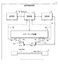
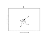
最初に、図1に示す基板検査装置1の構成について説明する。基板検査装置1は、検査装置の一例であって、基板100(プロービング対象の一例)の検査を実行可能に構成されている。具体的には、基板検査装置1は、同図に示すように、基板保持部2、プロービング機構3、プローブユニット4a,4b(以下、区別しないときには「プローブユニット4」ともいう)、撮像部5a,5b(以下、区別しないときには「撮像部5」ともいう)、測定部6、制御部7および記憶部8を備えて構成されている。なお、撮像部5および制御部7によって処理装置が構成される。
First, the configuration of the substrate inspection apparatus 1 shown in FIG. 1 will be described. The substrate inspection apparatus 1 is an example of an inspection apparatus, and is configured to be able to inspect a substrate 100 (an example of a probing target). Specifically, as shown in the figure, the substrate inspection apparatus 1 includes a
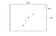
基板保持部2は、一例として、プロービング対象体としての基板100およびテスト基板200の外周部を挟持して、予め決められた保持位置において基板100およびテスト基板200を保持可能に構成されている。ここで、テスト基板200は、後述する位置ずれ量Eを特定する特定処理60において用いるテスト用の基板であって、一例として、プローブユニット4のプローブ41(図1参照)をプロービングさせたときに打痕S(図4参照)が形成される打痕シート201(一例として、感圧シート)が絶縁性を有する基板本体の上に取り付けられて構成されている。
As an example, the
プロービング機構3は、制御部7の制御に従い、基板保持部2によって保持されている基板100の表面100a(接触面に相当する)に平行な方向(XY方向)、および表面100aに垂直な方向(Z方向)にプローブ41を移動させることにより、表面100aに予め規定された規定位置Pp(図4参照)に対するプローブ41のプロービングを実行する。また、プロービング機構3は、撮像部5を上記したXYZ方向に移動させる移動処理を実行する。
The probing
プローブユニット4a,4bは、図1に示すように、プローブ41およびプローブ支持部42をそれぞれ備えて構成されている。プローブ41は、金属等の導電性材料で棒状に形成されている。プローブ支持部42は、図1に示すように、基板保持部2によって保持されている基板100の表面100aに垂直な方向に対して傾斜する姿勢でプローブ41を支持する。
As shown in FIG. 1, each of the
撮像部5a,5bは、制御部7の制御に従い、基板保持部2によって保持されているテスト基板200における打痕シート201の表面201a(被接触面)をテスト基板200の上方から撮像し、その撮像画像G(図5参照)の画像データDgを出力する撮像処理を実行する。この場合、撮像部5aはプローブユニット4aと共にプロービング機構3によって基板保持部2の上方においてXY方向に移動させられる。また、撮像部5bはプローブユニット4bと共にプロービング機構3によって基板保持部2の上方においてXYZ方向に移動させられる。
Under the control of the control unit 7, the
測定部6は、制御部7の制御に従って測定処理を実行し、プローブ41を介して入出力する電気信号に基づいて物理量(電圧や電流)を測定する。
The
制御部7は、基板検査装置1を構成する各部を制御する。具体的には、制御部7は、プロービング機構3によるプロービングおよび移動処理を制御する。また、制御部7は、撮像部5による撮像処理を制御する。また、制御部7は、処理部として機能し、基板保持部2に保持させたテスト基板200の打痕シート201の表面201aにおける規定位置Ppに対してプロービング機構3にプロービングを実行させたときに生じる打痕Sを撮像部5に撮像させると共に、撮像部5によって撮像された撮像画像Gを画像処理して打痕Sの位置(プロービング位置Pc)と規定位置Ppとの位置ずれ量E(図5参照)を特定する。
The control unit 7 controls each unit constituting the substrate inspection apparatus 1. Specifically, the control unit 7 controls probing and movement processing by the probing
記憶部8は、基板100に対してプローブ41をプロービングさせるべき位置として予め規定された規定位置Ppを示す規定位置データDpを記憶する。また、記憶部8は、制御部7によって特定される位置ずれ量Eを示す位置ずれ量データDeを記憶する。また、記憶部8は、撮像部5から出力された画像データDgを記憶する。さらに、記憶部8は、制御部7によって生成される図心データDcを記憶する。
The
次に、基板検査装置1を用いて基板100を検査する検査方法について、図面を参照して説明する。なお、発明の理解を容易とするため、撮像部5の取り付け誤差は、事前の調整によって解消されている(取り付け誤差がない状態とされている)ものとする。 Next, an inspection method for inspecting the substrate 100 using the substrate inspection apparatus 1 will be described with reference to the drawings. In order to facilitate understanding of the invention, it is assumed that the attachment error of the imaging unit 5 has been eliminated by prior adjustment (there is no attachment error).
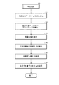
まず、基板100の検査に先立ち、プローブ41の取り付け誤差に相当する位置ずれ量Eを特定する。具体的には、テスト基板200の外周部を基板保持部2に挟持させてテスト基板200を保持させる。次いで、図外の操作部を操作して、特定処理の開始を指示する。これに応じて、制御部7は、図2に示す特定処理60を実行して、プローブユニット4aのプローブ41についての位置ずれ量Eを特定する。この特定処理60では、制御部7は、記憶部8から規定位置データDpを読み出す(ステップ61)。
First, prior to the inspection of the substrate 100, the positional deviation amount E corresponding to the attachment error of the
続いて、制御部7は、規定位置データDpに基づいて規定位置Ppの1つ(図4に示す規定位置Pp)を特定し、次いで、プロービング機構3を制御して、その規定位置Ppに対するプロービングを実行させる(ステップ62)。この際に、プローブ41の先端部41aがテスト基板200における打痕シート201の表面201aに接触し(先端部41aが表面201aを打撃し)、同図に示すように、打痕シート201の表面201aに打痕Sが形成される。
Subsequently, the control unit 7 specifies one of the specified positions Pp (the specified position Pp shown in FIG. 4) based on the specified position data Dp, and then controls the probing
続いて、制御部7は、プロービング機構3を制御して、プローブ41を上方に移動させた後に、規定位置Pp(打痕S)の上方の位置に撮像部5aを移動させる。
Subsequently, the control unit 7 controls the probing
次いで、制御部7は、撮像部5aを制御して撮像処理を実行させて(ステップ63)、打痕シート201の表面201aを撮像した撮像画像G(図5参照)の画像データDgを出力させる。
Next, the control unit 7 controls the
続いて、制御部7は、上記したプロービングの際にプローブ41の先端部41aが実際に位置したプロービング位置Pcに相当する打痕Sの位置(処理位置に相当し、以下、「打痕位置Ps」ともいう)を画像データDgに基づいて特定する打痕位置特定処理70(図3参照)を実行する(ステップ64)。
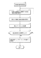
Subsequently, the control unit 7 determines the position of the dent S corresponding to the probing position Pc where the
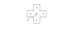
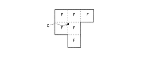
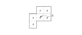
この打痕位置特定処理70では、制御部7は、図画像データDgを用いて撮像画像G(図5参照)を構成する画素Fの中から打痕Sを構成する画素Fを抽出する抽出処理を実行し(ステップ71)、次いで、抽出した画素Fの外周で規定される形状を打痕Sの形状として特定する。一例として、図6に示すように、画素Fが矩形(正方形)のときには、制御部7は、各画素Fにおける外周の辺を結ぶ形状を特定する。次いで、制御部7は、特定した打痕Sの形状の図心C(同図参照)の位置(座標)を算出する算出処理を実行する(ステップ72)。この場合、算出処理としては、公知の算出方法から任意の方法を用いることができる。続いて、制御部7は、図心Cの位置を示す図心データDcを生成して、記憶部8に記憶させる(ステップ73)。
In the dent
次いで、制御部7は、算出処理(上記したステップ72)を予め規定された複数回(一例として、5回)実行したか否かを判別する(ステップ74)。この時点では、算出処理の実行回数が1回であるため、制御部7は、上記した抽出処理(ステップ71)、算出処理(ステップ72)、および図心データDcを記憶させる処理(ステップ73)を実行した後、ステップ74を実行する。続いて、制御部7は、算出処理の実行回数が5回に達するまでステップ71〜ステップ74を繰り返して実行する。
Next, the control unit 7 determines whether or not the calculation process (step 72 described above) has been executed a plurality of times (for example, five times as an example) (step 74). At this point, since the number of executions of the calculation process is one, the control unit 7 stores the above-described extraction process (step 71), calculation process (step 72), and centroid data Dc (step 73). After executing
ここで、打痕Sの輪郭に接する画素Fや、輪郭の近傍に位置する画素Fが打痕Sを構成する画素Fとして抽出されるか否かは、制御部7による抽出処理の際のノイズ等によって変わることがある。つまり、図6〜図10に示すように、打痕Sを構成する画素Fとして抽出される画素Fは、制御部7が抽出処理を行う度に異なることがある。この結果、図6〜図10に示すように、画素Fの外周で規定される打痕Sの形状や、図心Cの位置も抽出処理や算出処理を行う度に異なることがある。このため、この基板検査装置1では、上記した抽出処理および算出処理を複数回実行して、後述する統計処理を行うことで、ノイズ等の影響の軽減を図っている。 Here, whether or not the pixel F in contact with the outline of the dent S and the pixel F located in the vicinity of the outline is extracted as the pixel F constituting the dent S depends on the noise during the extraction process by the control unit 7. May vary depending on etc. That is, as shown in FIGS. 6 to 10, the pixel F extracted as the pixel F constituting the dent S may be different each time the control unit 7 performs the extraction process. As a result, as shown in FIGS. 6 to 10, the shape of the dent S defined on the outer periphery of the pixel F and the position of the centroid C may be different each time the extraction process or the calculation process is performed. For this reason, in this board | substrate inspection apparatus 1, the above-mentioned extraction process and calculation process are performed in multiple times, and the statistical process mentioned later is performed and the influence of noise etc. is reduced.
次いで、制御部7は、ステップ74において、算出処理を5回実行したと判別したときには、統計処理の一例として、算出したn個(5個)の図心C(図11参照)の位置を示すXY座標を相加平均して、プロービング位置Pcとしての打痕位置Ps(処理位置)を特定する。具体的には、制御部7は、各図心CのX座標を相加平均してXaを算出すると共に、各図心CのY座標を相加平均してYaを算出する。続いて、制御部7は、XaをX座標、YaをY座標とする位置をプロービング位置Pcである打痕位置Ps(処理位置)として特定して(ステップ75)、打痕位置特定処理70を終了する。
Next, when it is determined in
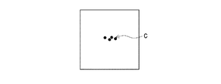
次いで、制御部7は、図2に示す特定処理60のステップ65を実行して、位置ずれ量Eを特定する。具体的には、制御部7は、図5に示すように、規定位置Ppと打痕位置Ps(プロービング位置Pc)との間のX方向の離間距離Ex、およびY方向の離間距離Eyを位置ずれ量Eとして特定する。続いて、制御部7は、位置ずれ量Eを示す位置ずれ量データDeを生成して記憶部8に記憶させて(ステップ66)、特定処理60を終了する。
Next, the control unit 7 executes
次いで、制御部7は、上記した特定処理60および打痕位置特定処理70を再び実行して、プローブユニット4bのプローブ41についての位置ずれ量Eを撮像部5bを用いて特定して位置ずれ量データDeを生成して記憶部8に記憶させる。
Next, the control unit 7 executes the above-described specifying
この場合、この基板検査装置1では、上記したように、打痕Sの形状の図心Cの位置(座標)を算出する算出処理を複数回(この例では、5回)実行して各図心Cの位置を統計処理して求めた位置をプロービング位置Pcとして位置ずれ量Eを特定している。このため、この基板検査装置1では、小形のプローブ41を用いて打痕シート201に形成される打痕Sが小さい場合においても、画像処理の際のノイズの影響を十分に軽減することが可能なため、プロービング位置Pcと規定位置Ppとの位置ずれ量Eを正確に特定することが可能となっている。
In this case, in the substrate inspection apparatus 1, as described above, the calculation process for calculating the position (coordinates) of the centroid C of the shape of the dent S is executed a plurality of times (in this example, five times). The position deviation amount E is specified with the position obtained by statistically processing the position of the heart C as the probing position Pc. For this reason, in this board | substrate inspection apparatus 1, even when the dent S formed in the dent sheet |
続いて、基板100の検査を行う。まず、テスト基板200を基板保持部2から取り外し、次いで、基板100の外周部を基板保持部2に挟持させて基板100を保持させる。続いて、図外の操作部を操作して、検査の開始を指示する。これに応じて、制御部7は、記憶部8から規定位置データDpおよび位置ずれ量データDeを読み出す。次いで、制御部7は、規定位置データDpに基づいてプローブユニット4a,4bの各プローブ41をプロービングさせるべき規定位置Ppを特定する。
Subsequently, the substrate 100 is inspected. First, the
続いて、制御部7は、規定位置Ppに対してプローブ41をプロービングさせる際のプローブユニット4a,4bの移動量を位置ずれ量データDeによって示される位置ずれ量Eで補正する。次いで、制御部7は、プロービング機構3を制御して、補正後の移動量だけプローブユニット4a,4bを移動させて規定位置Ppに対する各プローブ41のプロービングを実行させる。これにより、各プローブ41の取り付け誤差が補正された状態でプロービングが実行されるため、各規定位置Ppに各プローブ41の先端部41aが確実にプロービング(接触)させられる。
Subsequently, the control unit 7 corrects the amount of movement of the
続いて、制御部7は、測定部6を制御して測定処理を実行させる。この測定処理では、測定部6は、各プローブ41を介して測定用の電気信号を出力すると共に、プローブ41を介して入力した電気信号基づいて物理量(電圧や電流)を測定する。次いで、制御部7は、測定部6によって測定された物理量に基づいて基板100の良否を判定する。
Subsequently, the control unit 7 controls the
このように、この処理装置、基板検査装置1および位置ずれ量特定方法によれば、打痕Sの撮像画像Gを画像処理することによって打痕Sの形状の図心Cの位置を算出する算出処理を複数回実行し、各算出処理によって算出した複数の図心Cの位置を統計処理して求めた打痕位置Ps(処理位置)をプロービング位置Pcとして位置ずれ量Eを特定することにより、小形のプローブ41を用いることで打痕シート201に形成される打痕Sが小さいために打痕の形状が不明瞭な場合においても、画像処理の際のノイズの影響を十分に軽減することができるため、プロービング位置Pcと規定位置Ppとの位置ずれ量Eを正確に特定することができる。したがって、この基板検査装置1によれば、正確に特定したプロービング位置Pcと規定位置Ppとの位置ずれ量Eに基づいてプロービングの際のプローブユニット4a,4bの移動量を補正することで、プローブ41を規定位置Ppに確実にプロービングさせることができるため、基板100(プロービング対象)の検査を正確に行うことができる。
As described above, according to the processing apparatus, the substrate inspection apparatus 1, and the positional deviation amount specifying method, calculation is performed to calculate the position of the centroid C of the shape of the dent S by performing image processing on the captured image G of the dent S. By executing the process a plurality of times and specifying the displacement position E with the dent position Ps (process position) obtained by statistically processing the positions of the plurality of centroids C calculated by the respective calculation processes as the probing position Pc, Even if the shape of the dent is unclear because the dent S formed on the
また、この処理装置、基板検査装置1および位置ずれ量特定方法によれば、統計処理として複数の図心Cの位置を示す座標を相加平均して打痕位置Ps(処理位置)を求めることにより、複数の図心Cの位置が正規分布をしている場合に各図心Cによって代表される妥当な位置を打痕位置Psとすることができる。また、相加平均は、計算が簡易なため、打痕位置Psを求める処理の処理効率を十分に高めることができる。 Further, according to the processing apparatus, the substrate inspection apparatus 1 and the positional deviation amount specifying method, the dent position Ps (processing position) is obtained by arithmetically averaging coordinates indicating the positions of a plurality of centroids C as statistical processing. Thus, when the positions of a plurality of centroids C are normally distributed, an appropriate position represented by each centroid C can be set as the dent position Ps. In addition, since the arithmetic mean is easy to calculate, the processing efficiency of the processing for obtaining the dent position Ps can be sufficiently increased.
また、この処理装置、基板検査装置1および位置ずれ量特定方法によれば、撮像画像Gを構成する画素Fの中から打痕Sを構成する画素Fを抽出し、抽出した画素Fの外周で規定される形状を打痕Sの形状として図心Cの位置を算出することにより、簡易な手順で図心Cの位置を算出することができるため、図心Cの位置を算出する処理の処理効率を十分に高めることができる。 Further, according to the processing apparatus, the substrate inspection apparatus 1, and the positional deviation amount specifying method, the pixel F constituting the dent S is extracted from the pixels F constituting the captured image G, and the outer periphery of the extracted pixel F is extracted. Since the position of the centroid C can be calculated by a simple procedure by calculating the position of the centroid C using the prescribed shape as the shape of the dent S, the processing of the process of calculating the position of the centroid C is performed. Efficiency can be increased sufficiently.
なお、処理装置、検査装置および位置ずれ量特定方法の構成および方法は、上記の構成および方法に限定されない。例えば、統計処理として複数の図心Cの位置を相加平均して打痕位置Ps(処理位置)を求める例について上記したが、複数の図心Cの位置を相乗平均して(統計処理の他の一例)打痕位置Ps(処理位置)を求める構成および方法を採用することもできる。 Note that the configurations and methods of the processing device, the inspection device, and the positional deviation amount specifying method are not limited to the above configurations and methods. For example, the statistical processing is described above as an example in which the positions of a plurality of centroids C are arithmetically averaged to obtain the dent position Ps (processing position). Another example) A configuration and method for obtaining the dent position Ps (processing position) can also be adopted.
また、1つの規定位置Ppに対してプロービングを実行させて形成させた打痕Sについての位置ずれ量Eを特定する例について上記したが、複数の規定位置Ppに対してプロービングを実行させて形成させた複数の打痕Sについての位置ずれ量Eをそれぞれ特定する構成および方法を採用することもできる。この場合、複数の位置ずれ量Eを相加平均した値や相乗平均した値で規定位置Ppを補正することができる。また、複数の位置ずれ量Eを用いて、アフィン変換等の処理によって基板100の変形を特定して、規定位置Ppを補正する構成を採用することもできる。 In addition, the example of specifying the positional deviation amount E for the dent S formed by performing the probing with respect to one specified position Pp has been described above. However, the probing is performed with respect to the plurality of specified positions Pp. It is also possible to adopt a configuration and a method for specifying the positional deviation amount E for each of the plurality of dents S. In this case, the specified position Pp can be corrected with an arithmetic average value or a geometric average value of a plurality of positional deviation amounts E. In addition, it is possible to adopt a configuration in which the deformation of the substrate 100 is specified by a process such as affine transformation using a plurality of positional deviation amounts E, and the specified position Pp is corrected.
1 基板検査装置
3 プロービング機構
5a,5b 撮像部
6 測定部
7 制御部
41 プローブ
41a 先端部
100 基板
100a 表面
200 テスト基板
201 打痕シート
201a 表面
C 図心
E 位置ずれ量
G 撮像画像
Pc プロービング位置
Pp 規定位置
Ps 打痕位置
S 打痕
DESCRIPTION OF SYMBOLS 1 Board |
Claims (5)
前記保持位置に保持された前記プロービング対象の前記被接触面を撮像する撮像部と、
前記保持位置に保持させた前記プロービング対象としての打痕シートの前記被接触面における前記規定位置に対して前記プロービング機構に前記プロービングを実行させたときに生じる打痕の前記撮像部によって撮像された画像を用いて前記特定処理を実行する処理部とを備え、
前記処理部は、前記特定処理において、前記画像を画像処理することによって前記打痕の形状の図心の位置を算出する算出処理を複数回実行し、前記各算出処理によって算出した複数の図心の位置を統計処理して求めた処理位置を前記プロービング位置として前記位置ずれ量を特定する処理装置。 Probing position where the tip of the probe is actually located when the probe tip is brought into contact with a specified position on the contacted surface of the probe target to be probed by causing the probing mechanism to perform probe probing and the probe A processing device that executes a specific process for specifying a positional deviation amount from a specified position,
An imaging unit that images the contacted surface of the probing target held in the holding position;
An image of the dent formed when the probing mechanism executes the probing with respect to the specified position on the contacted surface of the dent sheet as the probing target held at the holding position was imaged. A processing unit that executes the specific process using an image,
In the specifying process, the processing unit executes a calculation process for calculating a position of a centroid of the shape of the impression by performing image processing on the image, and a plurality of centroids calculated by the calculation processes. A processing device that specifies the amount of displacement by using the processing position obtained by statistical processing of the position as the probing position.
前記保持位置に保持させた前記プロービング対象としての打痕シートの前記被接触面における前記規定位置に対して前記プロービング機構に前記プロービングを実行させたときに生じる打痕の画像を撮像し、当該画像を画像処理することによって前記打痕の形状の図心の位置を算出する算出処理を複数回実行し、前記各算出処理によって算出した複数の図心の位置を統計処理して求めた処理位置を前記プロービング位置として前記位置ずれ量を特定する位置ずれ量特定方法。 Probing position where the tip of the probe is actually located when the probe tip is brought into contact with a specified position on the contacted surface of the probe target to be probed by causing the probing mechanism to perform probe probing and the probe A positional deviation amount specifying method for specifying a positional deviation amount from a specified position,
An image of a dent formed when the probing mechanism performs the probing with respect to the specified position on the contacted surface of the dent sheet as the probing target held at the holding position, and the image A plurality of calculation processes for calculating the position of the centroid of the shape of the impression by performing image processing, and processing positions obtained by performing statistical processing on the positions of the plurality of centroids calculated by the respective calculation processes A positional deviation amount specifying method for specifying the positional deviation amount as the probing position.
Priority Applications (1)
| Application Number | Priority Date | Filing Date | Title |
|---|---|---|---|
| JP2015220013A JP6576216B2 (en) | 2015-11-10 | 2015-11-10 | Processing device, inspection device, and positional deviation amount specifying method |
Applications Claiming Priority (1)
| Application Number | Priority Date | Filing Date | Title |
|---|---|---|---|
| JP2015220013A JP6576216B2 (en) | 2015-11-10 | 2015-11-10 | Processing device, inspection device, and positional deviation amount specifying method |
Publications (2)
| Publication Number | Publication Date |
|---|---|
| JP2017090227A JP2017090227A (en) | 2017-05-25 |
| JP6576216B2 true JP6576216B2 (en) | 2019-09-18 |
Family
ID=58771520
Family Applications (1)
| Application Number | Title | Priority Date | Filing Date |
|---|---|---|---|
| JP2015220013A Active JP6576216B2 (en) | 2015-11-10 | 2015-11-10 | Processing device, inspection device, and positional deviation amount specifying method |
Country Status (1)
| Country | Link |
|---|---|
| JP (1) | JP6576216B2 (en) |
Family Cites Families (4)
| Publication number | Priority date | Publication date | Assignee | Title |
|---|---|---|---|---|
| JP3012726B2 (en) * | 1991-12-04 | 2000-02-28 | ロイヤルコントロールズ株式会社 | Ferrule eccentricity inspection device |
| JPH0829489A (en) * | 1994-07-18 | 1996-02-02 | Hioki Ee Corp | Error correction method between probes of XY system in-circuit tester |
| US6710798B1 (en) * | 1999-03-09 | 2004-03-23 | Applied Precision Llc | Methods and apparatus for determining the relative positions of probe tips on a printed circuit board probe card |
| KR20100089131A (en) * | 2009-02-03 | 2010-08-12 | 삼성전자주식회사 | Method of correcting positions of a prober and apparatus for performing the same |
-
2015
- 2015-11-10 JP JP2015220013A patent/JP6576216B2/en active Active
Also Published As
| Publication number | Publication date |
|---|---|
| JP2017090227A (en) | 2017-05-25 |
Similar Documents
| Publication | Publication Date | Title |
|---|---|---|
| KR102106349B1 (en) | Printed circuit board inspecting apparatus, method for detecting anomalry of solder paste and computer readable recording medium | |
| US9743527B2 (en) | Stencil programming and inspection using solder paste inspection system | |
| JP2013164381A (en) | Alignment method of substrate inspection device, and substrate inspection device | |
| JP6112896B2 (en) | Substrate inspection apparatus and correction information acquisition method | |
| JP2017015396A5 (en) | ||
| JP5875811B2 (en) | Substrate inspection apparatus and correction information acquisition method | |
| JP6550240B2 (en) | Coating agent inspection method, coating agent inspection device, coating agent inspection program, and computer readable recording medium recording the program | |
| JP6576216B2 (en) | Processing device, inspection device, and positional deviation amount specifying method | |
| JP2009019907A (en) | Inspection device | |
| JP6277347B2 (en) | Inspection apparatus and inspection method for flexible circuit board | |
| CN111397778A (en) | Stress detection method, device and system | |
| JP5955736B2 (en) | Substrate inspection apparatus and correction information acquisition method | |
| JP2013011569A (en) | Displacement amount identification device, displacement amount identification method, and displacement amount identification program | |
| JPH08262114A (en) | Method for controlling probe movement in circuit board inspection apparatus | |
| JP2009294155A (en) | Arm offset acquisition method | |
| JP6999327B2 (en) | Board inspection equipment | |
| JP6498564B2 (en) | Processing apparatus, substrate inspection apparatus, processing method, and substrate inspection method | |
| JP2013053968A (en) | Substrate inspection device and correction information acquisition method | |
| JPH07140088A (en) | Method of correcting unit movement amount of appearance inspection camera in circuit board inspection device | |
| JP2016102772A (en) | Circuit board inspection device and circuit board inspection method | |
| JP2009186330A (en) | Vibration detection method, appearance inspection method, and devices thereof | |
| JP4311240B2 (en) | Solder inspection apparatus and solder inspection method | |
| JP6058325B2 (en) | Substrate inspection apparatus and substrate inspection method | |
| JPH0829489A (en) | Error correction method between probes of XY system in-circuit tester | |
| JP6794215B2 (en) | Board inspection equipment |
Legal Events
| Date | Code | Title | Description |
|---|---|---|---|
| A621 | Written request for application examination |
Free format text: JAPANESE INTERMEDIATE CODE: A621 Effective date: 20180920 |
|
| A977 | Report on retrieval |
Free format text: JAPANESE INTERMEDIATE CODE: A971007 Effective date: 20190719 |
|
| TRDD | Decision of grant or rejection written | ||
| A01 | Written decision to grant a patent or to grant a registration (utility model) |
Free format text: JAPANESE INTERMEDIATE CODE: A01 Effective date: 20190730 |
|
| A61 | First payment of annual fees (during grant procedure) |
Free format text: JAPANESE INTERMEDIATE CODE: A61 Effective date: 20190820 |
|
| R150 | Certificate of patent or registration of utility model |
Ref document number: 6576216 Country of ref document: JP Free format text: JAPANESE INTERMEDIATE CODE: R150 |
|
| R250 | Receipt of annual fees |
Free format text: JAPANESE INTERMEDIATE CODE: R250 |
|
| R250 | Receipt of annual fees |
Free format text: JAPANESE INTERMEDIATE CODE: R250 |
|
| R250 | Receipt of annual fees |
Free format text: JAPANESE INTERMEDIATE CODE: R250 |