JP6574792B2 - LDMOS transistor with improved RDS × CGD and method for forming an LDMOS transistor with improved RDS × CGD - Google Patents
LDMOS transistor with improved RDS × CGD and method for forming an LDMOS transistor with improved RDS × CGD Download PDFInfo
- Publication number
- JP6574792B2 JP6574792B2 JP2016573708A JP2016573708A JP6574792B2 JP 6574792 B2 JP6574792 B2 JP 6574792B2 JP 2016573708 A JP2016573708 A JP 2016573708A JP 2016573708 A JP2016573708 A JP 2016573708A JP 6574792 B2 JP6574792 B2 JP 6574792B2
- Authority
- JP
- Japan
- Prior art keywords
- depth
- region
- dopant concentration
- semiconductor material
- back gate
- Prior art date
- Legal status (The legal status is an assumption and is not a legal conclusion. Google has not performed a legal analysis and makes no representation as to the accuracy of the status listed.)
- Active
Links
Images


Classifications
-
- H—ELECTRICITY
- H10—SEMICONDUCTOR DEVICES; ELECTRIC SOLID-STATE DEVICES NOT OTHERWISE PROVIDED FOR
- H10D—INORGANIC ELECTRIC SEMICONDUCTOR DEVICES
- H10D62/00—Semiconductor bodies, or regions thereof, of devices having potential barriers
- H10D62/10—Shapes, relative sizes or dispositions of the regions of the semiconductor bodies; Shapes of the semiconductor bodies
- H10D62/13—Semiconductor regions connected to electrodes carrying current to be rectified, amplified or switched, e.g. source or drain regions
- H10D62/149—Source or drain regions of field-effect devices
- H10D62/151—Source or drain regions of field-effect devices of IGFETs
- H10D62/156—Drain regions of DMOS transistors
- H10D62/157—Impurity concentrations or distributions
-
- H—ELECTRICITY
- H10—SEMICONDUCTOR DEVICES; ELECTRIC SOLID-STATE DEVICES NOT OTHERWISE PROVIDED FOR
- H10D—INORGANIC ELECTRIC SEMICONDUCTOR DEVICES
- H10D30/00—Field-effect transistors [FET]
- H10D30/01—Manufacture or treatment
- H10D30/021—Manufacture or treatment of FETs having insulated gates [IGFET]
- H10D30/0221—Manufacture or treatment of FETs having insulated gates [IGFET] having asymmetry in the channel direction, e.g. lateral high-voltage MISFETs having drain offset region or extended-drain MOSFETs [EDMOS]
-
- H—ELECTRICITY
- H10—SEMICONDUCTOR DEVICES; ELECTRIC SOLID-STATE DEVICES NOT OTHERWISE PROVIDED FOR
- H10D—INORGANIC ELECTRIC SEMICONDUCTOR DEVICES
- H10D30/00—Field-effect transistors [FET]
- H10D30/01—Manufacture or treatment
- H10D30/021—Manufacture or treatment of FETs having insulated gates [IGFET]
- H10D30/0223—Manufacture or treatment of FETs having insulated gates [IGFET] having source and drain regions or source and drain extensions self-aligned to sides of the gate
- H10D30/0227—Manufacture or treatment of FETs having insulated gates [IGFET] having source and drain regions or source and drain extensions self-aligned to sides of the gate having both lightly-doped source and drain extensions and source and drain regions self-aligned to the sides of the gate, e.g. lightly-doped drain [LDD] MOSFET or double-diffused drain [DDD] MOSFET
-
- H—ELECTRICITY
- H10—SEMICONDUCTOR DEVICES; ELECTRIC SOLID-STATE DEVICES NOT OTHERWISE PROVIDED FOR
- H10D—INORGANIC ELECTRIC SEMICONDUCTOR DEVICES
- H10D30/00—Field-effect transistors [FET]
- H10D30/01—Manufacture or treatment
- H10D30/021—Manufacture or treatment of FETs having insulated gates [IGFET]
- H10D30/028—Manufacture or treatment of FETs having insulated gates [IGFET] of double-diffused metal oxide semiconductor [DMOS] FETs
- H10D30/0281—Manufacture or treatment of FETs having insulated gates [IGFET] of double-diffused metal oxide semiconductor [DMOS] FETs of lateral DMOS [LDMOS] FETs
-
- H—ELECTRICITY
- H10—SEMICONDUCTOR DEVICES; ELECTRIC SOLID-STATE DEVICES NOT OTHERWISE PROVIDED FOR
- H10D—INORGANIC ELECTRIC SEMICONDUCTOR DEVICES
- H10D30/00—Field-effect transistors [FET]
- H10D30/60—Insulated-gate field-effect transistors [IGFET]
- H10D30/601—Insulated-gate field-effect transistors [IGFET] having lightly-doped drain or source extensions, e.g. LDD IGFETs or DDD IGFETs
- H10D30/603—Insulated-gate field-effect transistors [IGFET] having lightly-doped drain or source extensions, e.g. LDD IGFETs or DDD IGFETs having asymmetry in the channel direction, e.g. lateral high-voltage MISFETs having drain offset region or extended drain IGFETs [EDMOS]
-
- H—ELECTRICITY
- H10—SEMICONDUCTOR DEVICES; ELECTRIC SOLID-STATE DEVICES NOT OTHERWISE PROVIDED FOR
- H10D—INORGANIC ELECTRIC SEMICONDUCTOR DEVICES
- H10D30/00—Field-effect transistors [FET]
- H10D30/60—Insulated-gate field-effect transistors [IGFET]
- H10D30/64—Double-diffused metal-oxide semiconductor [DMOS] FETs
- H10D30/65—Lateral DMOS [LDMOS] FETs
-
- H—ELECTRICITY
- H10—SEMICONDUCTOR DEVICES; ELECTRIC SOLID-STATE DEVICES NOT OTHERWISE PROVIDED FOR
- H10D—INORGANIC ELECTRIC SEMICONDUCTOR DEVICES
- H10D62/00—Semiconductor bodies, or regions thereof, of devices having potential barriers
- H10D62/10—Shapes, relative sizes or dispositions of the regions of the semiconductor bodies; Shapes of the semiconductor bodies
- H10D62/124—Shapes, relative sizes or dispositions of the regions of semiconductor bodies or of junctions between the regions
- H10D62/125—Shapes of junctions between the regions
-
- H—ELECTRICITY
- H10—SEMICONDUCTOR DEVICES; ELECTRIC SOLID-STATE DEVICES NOT OTHERWISE PROVIDED FOR
- H10D—INORGANIC ELECTRIC SEMICONDUCTOR DEVICES
- H10D62/00—Semiconductor bodies, or regions thereof, of devices having potential barriers
- H10D62/10—Shapes, relative sizes or dispositions of the regions of the semiconductor bodies; Shapes of the semiconductor bodies
- H10D62/13—Semiconductor regions connected to electrodes carrying current to be rectified, amplified or switched, e.g. source or drain regions
- H10D62/149—Source or drain regions of field-effect devices
- H10D62/151—Source or drain regions of field-effect devices of IGFETs
-
- H—ELECTRICITY
- H10—SEMICONDUCTOR DEVICES; ELECTRIC SOLID-STATE DEVICES NOT OTHERWISE PROVIDED FOR
- H10D—INORGANIC ELECTRIC SEMICONDUCTOR DEVICES
- H10D62/00—Semiconductor bodies, or regions thereof, of devices having potential barriers
- H10D62/10—Shapes, relative sizes or dispositions of the regions of the semiconductor bodies; Shapes of the semiconductor bodies
- H10D62/17—Semiconductor regions connected to electrodes not carrying current to be rectified, amplified or switched, e.g. channel regions
- H10D62/351—Substrate regions of field-effect devices
- H10D62/357—Substrate regions of field-effect devices of FETs
- H10D62/364—Substrate regions of field-effect devices of FETs of IGFETs
- H10D62/371—Inactive supplementary semiconductor regions, e.g. for preventing punch-through, improving capacity effect or leakage current
-
- H—ELECTRICITY
- H10—SEMICONDUCTOR DEVICES; ELECTRIC SOLID-STATE DEVICES NOT OTHERWISE PROVIDED FOR
- H10D—INORGANIC ELECTRIC SEMICONDUCTOR DEVICES
- H10D62/00—Semiconductor bodies, or regions thereof, of devices having potential barriers
- H10D62/10—Shapes, relative sizes or dispositions of the regions of the semiconductor bodies; Shapes of the semiconductor bodies
- H10D62/17—Semiconductor regions connected to electrodes not carrying current to be rectified, amplified or switched, e.g. channel regions
- H10D62/393—Body regions of DMOS transistors or IGBTs
-
- H—ELECTRICITY
- H10—SEMICONDUCTOR DEVICES; ELECTRIC SOLID-STATE DEVICES NOT OTHERWISE PROVIDED FOR
- H10D—INORGANIC ELECTRIC SEMICONDUCTOR DEVICES
- H10D62/00—Semiconductor bodies, or regions thereof, of devices having potential barriers
- H10D62/10—Shapes, relative sizes or dispositions of the regions of the semiconductor bodies; Shapes of the semiconductor bodies
- H10D62/113—Isolations within a component, i.e. internal isolations
- H10D62/115—Dielectric isolations, e.g. air gaps
- H10D62/116—Dielectric isolations, e.g. air gaps adjoining the input or output regions of field-effect devices, e.g. adjoining source or drain regions
-
- H—ELECTRICITY
- H10—SEMICONDUCTOR DEVICES; ELECTRIC SOLID-STATE DEVICES NOT OTHERWISE PROVIDED FOR
- H10P—GENERIC PROCESSES OR APPARATUS FOR THE MANUFACTURE OR TREATMENT OF DEVICES COVERED BY CLASS H10
- H10P30/00—Ion implantation into wafers, substrates or parts of devices
- H10P30/20—Ion implantation into wafers, substrates or parts of devices into semiconductor materials, e.g. for doping
- H10P30/202—Ion implantation into wafers, substrates or parts of devices into semiconductor materials, e.g. for doping characterised by the semiconductor materials
- H10P30/204—Ion implantation into wafers, substrates or parts of devices into semiconductor materials, e.g. for doping characterised by the semiconductor materials into Group IV semiconductors
-
- H—ELECTRICITY
- H10—SEMICONDUCTOR DEVICES; ELECTRIC SOLID-STATE DEVICES NOT OTHERWISE PROVIDED FOR
- H10P—GENERIC PROCESSES OR APPARATUS FOR THE MANUFACTURE OR TREATMENT OF DEVICES COVERED BY CLASS H10
- H10P30/00—Ion implantation into wafers, substrates or parts of devices
- H10P30/20—Ion implantation into wafers, substrates or parts of devices into semiconductor materials, e.g. for doping
- H10P30/21—Ion implantation into wafers, substrates or parts of devices into semiconductor materials, e.g. for doping of electrically active species
-
- H—ELECTRICITY
- H10—SEMICONDUCTOR DEVICES; ELECTRIC SOLID-STATE DEVICES NOT OTHERWISE PROVIDED FOR
- H10P—GENERIC PROCESSES OR APPARATUS FOR THE MANUFACTURE OR TREATMENT OF DEVICES COVERED BY CLASS H10
- H10P30/00—Ion implantation into wafers, substrates or parts of devices
- H10P30/20—Ion implantation into wafers, substrates or parts of devices into semiconductor materials, e.g. for doping
- H10P30/22—Ion implantation into wafers, substrates or parts of devices into semiconductor materials, e.g. for doping using masks
- H10P30/221—Ion implantation into wafers, substrates or parts of devices into semiconductor materials, e.g. for doping using masks characterised by the angle between the ion beam and the mask
-
- H—ELECTRICITY
- H10—SEMICONDUCTOR DEVICES; ELECTRIC SOLID-STATE DEVICES NOT OTHERWISE PROVIDED FOR
- H10P—GENERIC PROCESSES OR APPARATUS FOR THE MANUFACTURE OR TREATMENT OF DEVICES COVERED BY CLASS H10
- H10P30/00—Ion implantation into wafers, substrates or parts of devices
- H10P30/20—Ion implantation into wafers, substrates or parts of devices into semiconductor materials, e.g. for doping
- H10P30/222—Ion implantation into wafers, substrates or parts of devices into semiconductor materials, e.g. for doping characterised by the angle between the ion beam and the crystal planes or the main crystal surface
Landscapes
- Insulated Gate Type Field-Effect Transistor (AREA)
- Thin Film Transistor (AREA)
Description
本願は、概してLDMOSトランジスタに関し、更に特定して言えば、Rds×Cgdが改善されたLDMOSトランジスタ、及びそのLDMOSトランジスタを形成する方法に関連する。 The present application relates generally to LDMOS transistors, and more particularly to LDMOS transistors with improved Rds × Cgd and methods of forming the LDMOS transistors.
金属酸化物半導体(MOS)トランジスタは、ソースと、ドレインと、ボディであって、そのチャネル領域がソースとドレインとの間にあり且つソース及びドレインに接するボディと、チャネル領域の上にありゲート誘電体層によりチャネル領域から隔離されるゲートとを有する、周知の半導体デバイスである。MOSトランジスタの2つのタイプは、n+ソースとp型チャネル領域を備えたドレイン領域とを有するNMOSトランジスタ、及び、p+ソースとn型チャネル領域を備えたドレイン領域とを有するPMOSトランジスタである。 A metal oxide semiconductor (MOS) transistor has a source, a drain, and a body, the channel region of which is between the source and the drain and is in contact with the source and drain, over the channel region and the gate dielectric. A well-known semiconductor device having a gate isolated from a channel region by a body layer. Two types of MOS transistors are NMOS transistors having an n + source and a drain region with a p-type channel region, and PMOS transistors having a drain region with a p + source and an n-type channel region.
オペレーションにおいて、ソース及びボディが接地されると、ドレイン・ソース電界を構築するため正の電圧がドレイン上に置かれ、閾値電圧より大きい電圧がゲート上に置かれ、ドレインからソースへ電流が流れる。ゲートが接地までプルダウンされるときなど、ゲート上に置かれる電圧が閾値電圧より小さいとき、電流は流れない。 In operation, when the source and body are grounded, a positive voltage is placed on the drain to build a drain-source field, a voltage greater than the threshold voltage is placed on the gate, and current flows from the drain to the source. When the voltage placed on the gate is less than the threshold voltage, such as when the gate is pulled down to ground, no current flows.
電流生成MOSトランジスタは、1.2Vから5Vまでわたる環境などの低電圧環境において一般的に用いられる。これに対し、高電圧MOSトランジスタは、例えば、10V〜400Vの範囲の電圧で動作するトランジスタである。一層高い電圧を扱うため、高電圧MOSトランジスタは低電圧MOSトランジスタよりも大きい。 Current generating MOS transistors are commonly used in low voltage environments, such as environments ranging from 1.2V to 5V. On the other hand, the high voltage MOS transistor is a transistor that operates at a voltage in the range of 10V to 400V, for example. In order to handle higher voltages, high voltage MOS transistors are larger than low voltage MOS transistors.
高電圧MOSトランジスタの一つのタイプは、横方向に拡散されたMOS(LDMOS)トランジスタとして知られている。LDMOSトランジスタは、ドレインドリフト領域も有するMOSトランジスタである。ドレインドリフト領域は、ドレイン及びチャネル領域に接し、ドレインとチャネル領域との間にあり、ドレインと同じ導電型であるが、ドレインより低いドーパント濃度を有する。オペレーションにおいて、ドレインドリフト領域は、ドレイン・ソース電界の大きさを低減する。 One type of high voltage MOS transistor is known as a laterally diffused MOS (LDMOS) transistor. An LDMOS transistor is a MOS transistor that also has a drain drift region. The drain drift region is in contact with the drain and the channel region, is between the drain and the channel region, has the same conductivity type as the drain, but has a lower dopant concentration than the drain. In operation, the drain drift region reduces the magnitude of the drain-source field.
高電流(例えば、10A及びそれ以上)及び高周波数(1〜10MHz及びそれより高い)LDMOSトランジスタに対する新たな性能指数(FOM)はRds×Cgdであり、これは、ドレイン・ソース抵抗(Rds)とゲート・ドレイン容量(Cgd)の積である。このFOMを改善するため、Rds値、Cgd値、又はこれら両方の値を低減することが望ましい。 A new figure of merit (FOM) for high current (eg, 10 A and higher) and high frequency (1-10 MHz and higher) LDMOS transistors is Rds × Cgd, which is the drain-source resistance (Rds) and It is the product of gate-drain capacitance (Cgd). In order to improve this FOM, it is desirable to reduce the Rds value, the Cgd value, or both.
Cgdの低減に対する一つのアプローチは、一つのゲートの代わりにスプリット又はステップゲートを用いることである。ステップ又はスプリットゲートを用いる少なくとも一つの例において、メインゲートと2つの順次薄くなる(progressively)ゲートとが用いられ、そのため、下にあるゲート誘電体層が、ゲートが置かれる位置がドレイン領域に一層近くなるにつれて一層厚くなるようにする。しかし、このアプローチの一つの欠点は、スプリット又はステップゲートは製造するのが困難であり高価であるという点である。また、スプリット又はステップゲートは、一層長いドレインドリフト領域を必要とし得、これは、増大されるRdsのため高速モバイル用途においてデバイスを制限する。 One approach to Cgd reduction is to use split or step gates instead of one gate. In at least one example using a step or split gate, a main gate and two progressively thin gates are used, so that the underlying gate dielectric layer is more layered in the drain region where the gate is placed. Thicker as it gets closer. However, one drawback of this approach is that split or step gates are difficult and expensive to manufacture. Also, split or step gates may require longer drain drift regions, which limits devices in high speed mobile applications due to increased Rds.
記載される例において、LDMOSトランジスタが、改善されたRds×Cgdを提供する。LDMOSトランジスタは、半導体材料、及び半導体材料内にあるドレインドリフト領域を含む。ドレインドリフト領域は、第1の導電型、第1の深さでピークに達する第1の水平ドーパント濃度、及び第2の深さでピークに達する第2のドーパント濃度を有する。第1の深さは、半導体材料の頂部表面から或る距離下方に測定される。第2の深さは、第1の深さから或る距離下方に測定される。LDMOSトランジスタはバックゲート領域も含み、バックゲート領域は、ドレインドリフト領域に接するように半導体材料内にある。バックゲート領域は、第2の導電型、第3の深さでピークに達する第3の水平ドーパント濃度、第4の深さでピークに達する第4の水平ドーパント濃度、及び第5の深さでピークに達する第5の水平ドーパント濃度を有する。第3の深さは、半導体材料の頂部表面から或る距離下方に測定される。第4の深さは、第3の深さから或る距離下方に測定される。第5の深さは、第4の深さから或る距離下方に測定される。また、LDMOSトランジスタは、半導体材料の頂部表面に接するゲート誘電体層と、ドレインドリフト領域及びバックゲート領域の直接的に上にあるゲート誘電体層に接し、そのゲート誘電体層の上にあるゲートとを含む。 In the example described, an LDMOS transistor provides an improved Rds × Cgd. An LDMOS transistor includes a semiconductor material and a drain drift region within the semiconductor material. The drain drift region has a first conductivity type, a first horizontal dopant concentration that reaches a peak at a first depth, and a second dopant concentration that reaches a peak at a second depth. The first depth is measured a distance below the top surface of the semiconductor material. The second depth is measured a distance below the first depth. The LDMOS transistor also includes a back gate region, which is in the semiconductor material so as to contact the drain drift region. The back gate region has a second conductivity type, a third horizontal dopant concentration that reaches a peak at a third depth, a fourth horizontal dopant concentration that reaches a peak at a fourth depth, and a fifth depth. It has a fifth horizontal dopant concentration that reaches a peak. The third depth is measured a distance below the top surface of the semiconductor material. The fourth depth is measured a distance below the third depth. The fifth depth is measured a distance below the fourth depth. The LDMOS transistor also has a gate dielectric layer in contact with the top surface of the semiconductor material and a gate dielectric layer directly over the drain drift region and the back gate region, and a gate over the gate dielectric layer. Including.
改善されたRds×Cgdを提供するLDMOSトランジスタを形成する或る方法において、この方法は、半導体材料内にドレインドリフト領域を形成することを含む。ドレインドリフト領域は、第1の導電型、第1の深さでピークに達する第1の水平ドーパント濃度、及び第2の深さでピークに達する第2のドーパント濃度を有する。第1の深さは、半導体材料の頂部表面から或る距離下方に測定される。第2の深さは、第1の深さから或る距離下方に測定される。この方法はまた、ドレインドリフト領域に接するように半導体材料内にバックゲート領域を形成することを含む。バックゲート領域は、第2の導電型、第3の深さでピークに達する第3の水平ドーパント濃度、第4の深さでピークに達する第4のドーパント濃度、及び第5の深さでピークに達する第5の水平ドーパント濃度を有する。第3の深さは、半導体材料の頂部表面から或る距離下方に測定される。第4の深さは、第3の深さから或る距離下方に測定される。第5の深さは、第4の深さから或る距離下方に測定される。この方法は更に、半導体材料の頂部表面に接するゲート誘電体層を形成すること、及びドレインドリフト領域及びバックゲート領域の直接的に上にあるゲート誘電体層に接し、そのゲート誘電体層の上にあるゲートを形成することを含む。 In one method of forming an LDMOS transistor that provides improved Rds × Cgd, the method includes forming a drain drift region in the semiconductor material. The drain drift region has a first conductivity type, a first horizontal dopant concentration that reaches a peak at a first depth, and a second dopant concentration that reaches a peak at a second depth. The first depth is measured a distance below the top surface of the semiconductor material. The second depth is measured a distance below the first depth. The method also includes forming a back gate region in the semiconductor material in contact with the drain drift region. The back gate region has a second conductivity type, a third horizontal dopant concentration that reaches a peak at a third depth, a fourth dopant concentration that reaches a peak at a fourth depth, and a peak at a fifth depth Having a fifth horizontal dopant concentration of The third depth is measured a distance below the top surface of the semiconductor material. The fourth depth is measured a distance below the third depth. The fifth depth is measured a distance below the fourth depth. The method further includes forming a gate dielectric layer in contact with the top surface of the semiconductor material, and in contact with the gate dielectric layer directly over the drain drift region and the back gate region, over the gate dielectric layer. Forming a gate on the substrate.
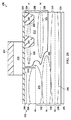
図1は、例示の実施例に従ったLDMOSトランジスタ100の一例の断面図を示す。これ以降に更に詳細に説明するように、LDMOSトランジスタ100は、ドレインドリフト領域と隣接するステップ形状のバックゲート領域との両方において複数の注入を用いることによりRds×Cgdを改善する。
FIG. 1 shows a cross-sectional view of an example of an
図1に示すように、LDMOSトランジスタ100は、基板又はエピタキシャル層などの半導体材料110、及び半導体材料110内にあるドレインドリフト領域112を含む。ドレインドリフト領域112は、第1の導電型と2つの水平ドーパント濃度ピークとを有し、2つの水平ドーパント濃度ピークは、半導体材料110の頂部表面114から下方に或る距離測定された深さD1における第1のピーク、及び深さD1から下方に或る距離測定された深さD2における第2のピークである。この例では、ドレインドリフト領域112はn導電型を有する。
As shown in FIG. 1, the
深さD1は、半導体材料110の頂部表面114から深さD1まで下方に延在するドリフト頂部120を画定する。ドリフト頂部120は或るドーパント濃度プロファイルを有し、このプロファイルにおいて、ドーパント濃度は、増大する深さと共に増大する。この例では、ドリフト頂部120は、半導体材料110の頂部表面114における低ドーパント濃度から、深さD1における高ドーパント濃度まで、継続的に増大する。また、ドリフト頂部120内の最大ドーパント濃度は深さD1にある。
The depth D1 defines a
深さD1及び深さD2は、深さD1から深さD2まで下方に延在するドリフト中間部124を画定する。ドリフト中間部124は或るドーパント濃度プロファイルを有し、このプロファイルにおいて、ドーパント濃度はまず、増大する深さと共に減少し、その後、増大する深さと共に増大する。
The depth D1 and the depth D2 define a drift
この例では、ドリフト中間部124は、深さD1における高ドーパント濃度から深さD1とD2の間の或る地点における一層低いドーパント濃度まで継続的に減少し、その後、深さD2における一層高いドーパント濃度まで継続的に増大する。また、ドリフト中間部124内の2つの最大ドーパント濃度は、深さD1及びD2にある。
In this example, drift
深さD2はまた、深さD2から或る距離下方に延在するドリフト底部126を画定する。ドリフト底部126は或るドーパント濃度プロファイルを有し、このプロファイルにおいて、ドーパント濃度は、深さD2から、増大する深さと共に減少する。この例では、ドリフト底部126は、深さD2における高ドーパント濃度から一層低いドーパント濃度まで継続的に減少する。また、ドリフト底部126内の最大ドーパント濃度は、深さD2にある。
The depth D2 also defines a
図1に更に示すように、LDMOSトランジスタ100はまた、ドレインドリフト領域112に接するように半導体材料110内にあるバックゲート領域128を含む。バックゲート領域128は、第2の導電型、及び、同じ導電型の3つの水平ドーパント濃度ピークに対応するステップ形状を有する。これらの3つの水平ドーパント濃度ピークは、半導体材料110の頂部表面114から下方に或る距離測定された深さD3におけるピーク、深さD3から下方に或る距離測定された深さD4におけるピーク、及び深さD4から下方に或る距離測定された深さD5におけるピークである。この例では、バックゲート領域128はp導電型を有する。
As further shown in FIG. 1, the
深さD3は、半導体材料110の頂部表面114から深さD3まで下方に延在するバックゲート頂部130を画定する。バックゲート頂部130は或るドーパント濃度プロファイルを有し、このプロファイルにおいて、ドーパント濃度は、増大する深さと共に増大する。この例では、バックゲート頂部130は、半導体材料110の頂部表面114における低ドーパント濃度から、深さD3における高ドーパント濃度まで、継続的に増大する。また、バックゲート頂部130内の最大ドーパント濃度は、深さD3にある。
The depth D3 defines a
深さD3及びD4はまた、深さD3から深さD4まで下方に延在するバックゲート中間部134を画定する。バックゲート中間部134は或るドーパント濃度プロファイルを有し、このプロファイルにおいて、ドーパント濃度は、まず、増大する深さと共に減少し、その後、増大する深さと共に増大する。
Depths D3 and D4 also define a backgate
この例では、バックゲート中間部134は、深さD3における高ドーパント濃度から、深さD3とD4の間の或る地点における一層低いドーパント濃度まで、継続的に減少し、その後、深さD4における一層高いドーパント濃度まで継続的に増大する。また、バックゲート中間部134内の2つの最大ドーパント濃度は、深さD3及びD4にある。
In this example, the backgate middle 134 continuously decreases from a high dopant concentration at depth D3 to a lower dopant concentration at some point between depths D3 and D4, and then at depth D4. It continuously increases to higher dopant concentrations. Further, the two maximum dopant concentrations in the back gate
深さD4及び深さD5は、深さD4から深さD5まで下方に延在するバックゲート中間部136を画定する。バックゲート中間部136は或るドーパント濃度プロファイルを有し、このプロファイルにおいて、ドーパント濃度は、まず、増大する深さと共に減少し、その後、増大する深さと共に増大する。
The depth D4 and the depth D5 define a back gate
この例では、バックゲート中間部136は、深さD4における高ドーパント濃度から、深さD4とD5の間の或る地点における一層低いドーパント濃度まで、継続的に減少し、その後、深さD5における一層高いドーパント濃度まで継続的に増大する。また、バックゲート中間部136内の2つの最大ドーパント濃度は、深さD4及びD5にある。 In this example, the backgate middle 136 continuously decreases from a high dopant concentration at depth D4 to a lower dopant concentration at some point between depths D4 and D5, and then at depth D5. It continuously increases to higher dopant concentrations. Also, the two maximum dopant concentrations in the back gate middle 136 are at depths D4 and D5.
深さD5は更に、深さD5から或る距離下方に延在するバックゲート底部138を画定する。バックゲート底部138は或るドーパント濃度プロファイルを有し、このプロファイルにおいて、ドーパント濃度は、深さD5から、増大する深さと共に減少する。この例では、バックゲート底部138は、深さD5における高ドーパント濃度から一層低いドーパント濃度まで継続的に減少する。図示するように、深さD3は深さD1と深さD2の間にある。また、深さD4は深さD2より下にある。また、バックゲート領域128のバックゲート中間部136及びバックゲート底部138の一部は、ドレインドリフト領域112の直接的に下にある。
The depth D5 further defines a
図1に更に示すように、LDMOSトランジスタ100は、半導体材料110内にある一対のシャロートレンチアイソレーション(STI)領域140を含む。STI領域140は、深さD1より下にある一層低い表面142を有する。この例では、STI領域140はまた、半導体材料110の頂部表面114と実質的に同じ平面にある頂部表面を有する。
As further shown in FIG. 1,
LDMOSトランジスタ100は更に、いずれも半導体材料110内にある、ドレイン領域150、ソース領域152、及び表面領域154を含む。第1の導電型を有するドレイン領域150は、ドレインドリフト領域112に接するようにSTI領域140間にある。ドレイン領域150は、ドレインドリフト領域112の最高ドーパント濃度より実質的に大きいドーパント濃度を有する。この例では、ドレイン領域150はn+領域として実装される。
The
ソース領域152は、同じく第1の導電型を有し、バックゲート領域128に接する。ソース領域152は、ドレイン領域150のドーパント濃度に実質的に等しいドーパント濃度を有する。この例では、ソース領域152はn+領域として実装される。
The
表面領域154は、同じく第1の導電型を有し、半導体材料110の頂部表面114、バックゲート領域128、及びソース領域152に接し、また、バックゲート領域128の一部の直接的に上にある。表面領域154は、ドレインドリフト領域112の最高ドーパント濃度より実質的に大きいドーパント濃度を有する。この例では、表面領域154はn+領域として実装される。(表面領域154は任意選択で省かれてもよい。)
The
LDMOSトランジスタ100はまた、バックゲート領域128に接するように半導体材料110内にあるボディコンタクト領域156を含む。ボディコンタクト領域156は、第2の導電型、及びバックゲート領域128の最高ドーパント濃度より実質的に大きいドーパント濃度を有する。この例では、ボディコンタクト領域156はp+領域として実装される。
The
図1に更に示されるように、LDMOSトランジスタ100は、半導体材料110の頂部表面114に接するゲート誘電体層160と、ゲート誘電体層160に接しゲート誘電体層160の上にあるゲート162と、ゲート162に接しゲート162を横方向に囲む側壁スペーサ164とを含む。バックゲート領域128は、ドレインドリフト領域112とソース領域152との間にあり、且つ、ドレインドリフト領域112及びソース領域152に接する、チャネル領域166を含む。ゲート162は、ドレインドリフト領域112及びバックゲート領域128のチャネル領域166の直接的に上にある。
As further shown in FIG. 1, the
オペレーションにおいて、ソース領域152及びボディコンタクト領域156が接地されると、ドレイン・ソース電界を構築するために16Vなどの正の電圧がドレイン領域150上に置かれ、閾値電圧より大きい電圧がゲート162上に置かれ、電流がドレイン領域150からソース領域152へ流れる。ゲート162が接地までプルダウンされるときなど、ゲート162上に置かれる電圧が閾値電圧より小さいとき、電流は流れない。
In operation, when
例示の実施例の利点の一つは、半導体材料110の頂部表面114における又はその直下のドリフト頂部120の領域が、深さと共に増大する、低いドーパント濃度を有するという点である。半導体材料110の頂部表面114におけるまたはその近辺の低いドーパント濃度の領域を用いることにより、ゲート・ドレイン容量Cgdが低減され得、Rds×Cgdが改善される。例示の実施例の別の利点は、深さD1及びD2における一層高いドーパント濃度がドレイン・ソース抵抗Rdsを低減するという点であり、これにより、Rds×Cgdが更に改善される。
One advantage of the illustrated embodiment is that the region of the
また、ドレインドリフト領域112は、ドリフト頂部120及びドリフト中間部124内の一層低いドーパント濃度領域の存在に起因して、ドレイン・ソース電界の大きさを低減し続ける。ドレイン・ソース抵抗Rds対ドレイン・ソース降伏電圧(BV)は、深さD2における高ドーパント濃度の水平領域における電荷を平衡させるためにドリフト底部126とバックゲート中間部136との間の相互作用も用いることによって、最も良好にトレードオフされる。
Also, the
例示の実施例の更なる利点は、ゲート162の下にある深さD1における高ドーパント濃度の水平領域が比較的大きく、これにより、チャネル抵抗及びJFET抵抗が低減されるという点である。JFET抵抗は、デプリーション領域の幅がドレイン150及びゲート162上の電圧と共に変化するチャネル166に近接する表面下領域に関連付けられる抵抗である。
A further advantage of the illustrated embodiment is that the high dopant concentration horizontal region at the depth D1 below the
また、深さD1及びD2における高ドーパント濃度の水平領域における表面は、低減されたCgdのため容易に空乏化される。また、増大されたドレイン電圧では、深さD3及びD4における高ドーパント濃度の水平領域のステップ形状エリアは、ゲート162の下にある深さD1及びD2における高ドーパント濃度の水平領域における増大する電界をスクリーンし得る。この現象は、デバイスドレイン・ソース降伏電圧を増大させるためにドレインドリフト領域112とバックゲート領域128との間の電荷バランスと共に働くか、又は、ターゲットとされるデバイスドレイン・ソース降伏電圧で、ドレインドリフト領域112長さ(STI領域140の一層低い表面142の真下のドリフト領域)が、低減されるRdsのために低減され得、これにより、総Rds×Cgdが改善される。そのため、例示の実施例は、Rds値及びCgd値両方を低減することによりRds×Cgdを改善する。
Also, the surface in the horizontal region of high dopant concentration at depths D1 and D2 is easily depleted due to the reduced Cgd. Also, at the increased drain voltage, the step shape area of the high dopant concentration horizontal region at depths D3 and D4 causes an increasing electric field in the high dopant concentration horizontal region at depths D1 and D2 below
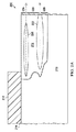
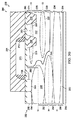
図2A〜図2Gは、例示の実施例に従ってLDMOSトランジスタ構造を形成する方法200の一例の一連の断面図を示す。方法200は、基板又はエピタキシャル層などの、従来と同様に形成された半導体材料210を用いる。
2A-2G illustrate a series of cross-sectional views of an
方法200は、半導体材料210内にドレインドリフト領域212を形成することにより始まる。ドレインドリフト領域212は、第1の導電型、及び2つの水平ドーパント濃度ピークを有する。2つの水平ドーパント濃度ピークは、半導体材料210の頂部表面214から下方へ或る距離測定された深さD1における第1のピーク、及び深さD1から下方へ或る距離測定された深さD2における第2のピークである。この例では、ドレインドリフト領域212はn導電型を有するように形成される。
The
ドレインドリフト領域212は、まず、パターニングされたフォトレジスト層216を半導体材料210上に形成することによって形成され得る。パターニングされたフォトレジスト層216は、従来のように形成され、この方式は、フォトレジストの層を堆積すること、パターニングされた画像をフォトレジストの層上に形成するために、マスクとして知られるパターニングされた黒/透明ガラスプレートを介して光を投射すること、及び光への曝露により軟化された、イメージングされたフォトレジスト領域を取り除くことを含む。
The
パターニングされたフォトレジスト層216が形成された後、上部領域220を形成するために、パターニングされたフォトレジスト層216を介してドーパントが半導体材料210に注入される。上部領域220は、深さD1でピークに達する水平ドーパント濃度を有する。この例では、n型上部領域220を形成するためにヒ素が注入される。ヒ素ドーパントは、例えば、4×10¹²〜8×10¹²のドーズ量及び200keV〜350keVのエネルギーで注入され得る。
After the patterned
パターニングされたフォトレジスト層216がまだその場にある状態で、今度は下部領域222を形成するために、ドーパントが再び、フォトレジスト層216を介して半導体材料210に注入される。下部領域222は、深さD2でピークに達する水平ドーパント濃度を有する。この例では、n型下部領域222を形成するためにリンが注入される。このリンドーパントは、例えば、8×10¹²〜2×10¹³のドーズ量及び100keV〜400keVのエネルギーで注入され得る。
With the patterned
下部領域222が形成された後、パターニングされたフォトレジスト層216は、アッシングプロセスなどの従来のように取り除かれる。これに続いて、熱駆動プロセスが、ドーパントを拡散及び活性化して、ドレインドリフト領域212の形成を完了する。熱駆動プロセスは、1100℃で90分間、又は例えば、1125℃で50分間、又は1050℃で270分間などの同等の条件の、熱処理を含み得る。
After the
深さD1は、半導体材料210の頂部表面214から深さD1まで下方に延在するドリフト頂部224を画定する。ドリフト頂部224の一部が熱駆動プロセスの間ドープされ、これにより、ドーパントが、上部領域220から上方にドリフト頂部224内に拡散される。
The depth D1 defines a
ドリフト頂部224は或るドーパント濃度プロファイルを有し、このプロファイルにおいて、ドーパント濃度は、増大する深さと共に増大する。この例では、ドリフト頂部224は、半導体材料210の頂部表面214における低ドーパント濃度から、深さD1における高ドーパント濃度まで、継続的に増大する。また、ドリフト頂部224内の最大ドーパント濃度は深さD1にある。
The
深さD1及び深さD2は、深さD1から深さD2まで下方に延在するドリフト中間部226を画定する。ドリフト中間部226の一部が熱駆動プロセスの間ドープされ、これにより、ドーパントが、上部領域220から下方に拡散され、下部領域222の一部から上方にドリフト中間部226内に拡散される。
The depth D1 and the depth D2 define a drift
ドリフト中間部226は或るドーパント濃度プロファイルを有し、このプロファイルにおいて、ドーパント濃度は、まず、増大する深さと共に減少し、その後、増大する深さと共に増大する。この例では、ドリフト中間部226は、深さD1における高ドーパント濃度から、深さD1及びD2間の或る地点における一層低いドーパント濃度まで、継続的に減少し、その後、深さD2における一層高いドーパント濃度まで継続的に増大する。また、ドリフト中間部226内の2つの最大ドーパント濃度は、深さD1及びD2にある。
The drift middle 226 has a dopant concentration profile in which the dopant concentration first decreases with increasing depth and then increases with increasing depth. In this example, the drift middle 226 continuously decreases from a high dopant concentration at depth D1 to a lower dopant concentration at some point between depths D1 and D2, and then higher at depth D2. Continuously increases to dopant concentration. Further, the two maximum dopant concentrations in the drift
深さD2はまた、深さD2から或る距離下方に延在するドリフト底部228を画定する。ドリフト底部228は熱駆動プロセスの間ドープされ、これにより、ドーパントが、下部領域222から下方に底部228内に拡散される。(上部及び下部領域220及び222が形成される順は、逆にされてもよい。)
The depth D2 also defines a
ドリフト底部228は或るドーパント濃度プロファイルを有し、このプロファイルにおいて、ドーパント濃度は、深さD2から、増大する深さと共に減少する。この例では、ドリフト底部228は、深さD2における高ドーパント濃度から一層低いドーパント濃度まで継続的に減少する。また、ドリフト底部228内の最大ドーパント濃度は深さD2にある。
The
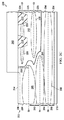
図2Bに示すように、ドレインドリフト領域212が形成された後、一対のシャロートレンチアイソレーション(STI)領域230が、ドレインドリフト領域212に接するように半導体材料210に形成される。STI領域230は従来のように形成され得る。例えば、半導体材料210の上にハードマスクが形成され得る。ハードマスクが形成された後、半導体材料210において複数のトレンチを形成するように、半導体材料210がハードマスクを介してエッチングされる。次に、ハードマスクが取り除かれ、トレンチを充填するように半導体材料210の頂部表面上に非導電性の材料が堆積される。半導体材料210の頂部表面上の非導電性の材料は、その後、トレンチにおけるSTI領域230を残すように、化学機械的平坦化(CMP)プロセスなどにより、取り除かれる。
As shown in FIG. 2B, after the
図2Bに更に示すように、STI領域230が形成された後、ドープされた領域232が次に、半導体材料210内に形成される。ドープされた領域232は、第2の導電型のバックゲート領域234、及びバックゲート領域234に接する第1の導電型の表面領域236を有する。
As further shown in FIG. 2B, after the
バックゲート領域234は、3つのドーパント濃度に対応するステップ形状を有するように形成され、3つのドーパント濃度は、半導体材料210の頂部表面から深さD3下方のピーク、一層低い深さD4のピーク、及び更に一層低い深さD5のピークである。この例では、バックゲート領域234はp導電型を有し、表面領域236はn導電型を有する。
The
バックゲート領域234は、ドレインドリフト領域212の底部228に接し、それより下にある埋め込み領域240を形成するように、先ず、ドーパントを半導体材料210にブランケット注入することによって形成され得る。埋め込み領域240は、深さD5でピークに達するドーパント濃度を有する。この例では、p型埋め込み領域234を形成するためにボロンが注入される。ボロンドーパントは、例えば、1×10¹²〜9×10¹³のドーズ量及び400keV〜900keVのエネルギーで注入され得る。
The
図2Cに示すように、埋め込み領域240が形成された後、パターニングされたフォトレジスト層242が従来のように半導体材料210上に形成される。パターニングされたフォトレジスト層242が形成された後、ドーパントは、中間領域244を形成するように、パターニングされたフォトレジスト層242を介して半導体材料210に角度注入(angle implanted)される。中間領域244は、深さD4でピークに達するドーパント濃度を有する。この例では、中間領域244を形成するためにボロンが注入される。ボロンドーパントは、例えば、2×10¹³〜4×10¹³のドーズ量及び300keV〜600keVのエネルギーで注入され得る。
As shown in FIG. 2C, after the buried
パターニングされたフォトレジスト層242がまだその場にある状態で、ボディ領域246を形成するために、ドーパントが再び、パターニングされたフォトレジスト層242を介して半導体材料210に注入される。ボディ領域246は、深さD3でピークに達するドーパント濃度を有する。この例では、ボディ領域246を形成するためにボロンが注入される。ボロンドーパントは、例えば、5×10¹³〜3×10¹⁴のドーズ量及び70keV〜300keVのエネルギーで注入され得る。
With the patterned
ボディ領域246が形成された後、バックゲート領域234のサイズを低減するため及び表面領域236を形成するために、ドーパントが再び、パターニングされたフォトレジスト層242を介して半導体材料210に注入される。表面領域236は、半導体材料210の頂部表面214に接し、ボディ領域246の上にある。この例では、表面領域236を形成するためにヒ素が注入される。ヒ素ドーパントは、例えば、5×10¹³〜1×10¹⁵のドーズ量及び30keV〜160keVのエネルギーで注入され得る。(表面領域236の形成は任意選択で省かれてもよい。)
After the
この注入の後、パターニングされたフォトレジスト層242が従来のように取り除かれる。これに続いて、ドーパントを拡散及び活性化するため、そして、ドープされた領域232、バックゲート領域234、及び表面領域236の形成を完了するために、熱駆動プロセスが実施される。この例では、表面領域236及びそのすぐ周りのエリアは、熱駆動の結果n型導電性を有し、一方、バックゲート領域234は、熱駆動の結果p型導電性を有する。(ドレインドリフト領域212及びドープされた領域232が形成される順は、逆にされてもよい。)
After this implantation, the patterned
深さD3は、半導体材料110の頂部表面114から深さD3まで下方に延在する基板頂部250を画定する。基板頂部250は、表面領域236より下であり表面領域236に近接する或るドーパント濃度プロファイルを有し、このプロファイルにおいて、ドーパント濃度は、増大する深さと共に増大する。この例では、基板頂部250は、表面領域236より下であり表面領域236に近接する低ドーパント濃度から、深さD3における高ドーパント濃度まで、継続的に増大する。また、基板頂部250内の最大ドーパント濃度は深さD3にある。
The depth D3 defines a
深さD3及び深さD4は、深さD3から深さD4まで下方に延在する基板中間部252を画定する。基板中間部252は或るドーパント濃度プロファイルを有し、このプロファイルにおいて、ドーパント濃度は、まず、増大する深さと共に減少し、その後、増大する深さと共に増大する。
The depth D3 and the depth D4 define a substrate
この例では、基板中間部252は、深さD3における高ドーパント濃度から、深さD3とD4間との或る地点における一層低いドーパント濃度まで、継続的に減少し、その後、深さD4における一層高いドーパント濃度まで継続的に増大する。また、基板中間部252内の2つの最大ドーパント濃度は、深さD3及びD4にある。
In this example, the substrate intermediate 252 continuously decreases from a high dopant concentration at depth D3 to a lower dopant concentration at some point between depths D3 and D4, and then a further layer at depth D4. It continuously increases to a high dopant concentration. Also, the two maximum dopant concentrations in the substrate
深さD4及び深さD5は、深さD4から深さD5まで下方に延在する基板中間部254を画定する。基板中間部254は或るドーパント濃度プロファイルを有し、このプロファイルにおいて、ドーパント濃度は、まず、増大する深さと共に減少し、その後、増大する深さと共に増大する。
The depth D4 and the depth D5 define a substrate
この例では、基板中間部254は、深さD4における高ドーパント濃度から、深さD4とD5との間の或る地点における一層低いドーパント濃度まで、継続的に減少し、その後、深さD5における一層高いドーパント濃度まで継続的に増大する。また、基板中間部254内の2つの最大ドーパント濃度は、深さD4及びD5にある。
In this example, the substrate intermediate 254 continuously decreases from a high dopant concentration at depth D4 to a lower dopant concentration at some point between depths D4 and D5, and then at depth D5. It continuously increases to higher dopant concentrations. Also, the two maximum dopant concentrations in the substrate
深さD5はまた、深さD5から或る距離下方に延在する基板底部256を画定する。基板底部256は或るドーパント濃度プロファイルを有し、このプロファイルにおいて、ドーパント濃度は、深さD5から、増大する深さと共に減少する。この例では、基板底部256は、深さD5における高ドーパント濃度から一層低いドーパント濃度まで低減する。図示するように、深さD3は、深さD1と深さD2との間にある。また、深さD4は深さD2より下にある。また、第2の(p)導電型のバックゲート領域234の一部が、ドレインドリフト領域212の直接的に下にある。
The depth D5 also defines a
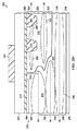
図2Dに示すように、ドープされた領域232が形成されると、方法200は次に、半導体材料210の頂部表面214上にゲート誘電体層260を形成する。例えば、希釈フッ化水素酸を用いるウェットエッチングのクリーンアップエッチングが、半導体材料210の頂部表面上の如何なる不要な酸化物も除くために、ゲート誘電体層260を形成する前に実施され得る。
As shown in FIG. 2D, once the doped
ゲート誘電体層260は、熱成長された二酸化シリコンで実装され得、用いられる電圧に従って変化する厚みを有する。例えば、ゲート誘電体層260は、5Vゲートオペレーションをサポートするために、12〜15nmの熱成長された二酸化シリコンを有し得る。ゲート誘電体層260は、シリコンオキシナイトライド又はハフニウム酸化物などの他の誘電性材料の付加的な層を含み得る。
The
これに続いて、ゲート材料262の層が、ゲート誘電体層260上に堆積される。ゲート材料262の層は、100〜200nmのポリシリコン、及び場合によっては、100〜200nmのタングステンシリサイドなどのポリシリコン上の金属シリサイドの層、を含み得る。ゲート材料262の層を実装するために用いることができる他の材料もこの例の範囲内にある。次に、パターニングされたフォトレジスト層264が、従来のようにゲート材料262の層の上に形成される。
Following this, a layer of
図2Eに示すように、パターニングされたフォトレジスト層264が形成された後、ゲート材料262の層の露出された領域は、ゲート誘電体層260を露出させるため及びゲート270を形成するために、従来のようにエッチングされる。エッチングに続いて、パターニングされたフォトレジスト層264が従来のように取り除かれる。
After the patterned
図2Fに示すように、パターニングされたフォトレジスト層264が取り除かれた後、ゲート側壁スペーサ272が、ゲート270の横方向表面上に従来のように形成される。ゲート側壁スペーサ272は、半導体デバイスの頂部表面の上に二酸化シリコンのコンフォーマル層を50〜150nmの厚み形成すること、及びその後、反応性イオンエッチング(RIE)プロセスなどの異方性エッチプロセスを用いて水平表面から二酸化シリコンを取り除くことによって形成され得る。
As shown in FIG. 2F, after the patterned
図2Fに更に示すように、次に、パターニングされたフォトレジスト層274が、ゲート誘電体層260及びゲート270上に従来のように形成される。この後、ソース領域280及びドレイン領域282を形成するために、ドレインドリフト領域212と同じ導電型を有するドーパントが、パターニングされたフォトレジスト層274を介して注入される。ソース領域280は、バックゲート領域234及び表面領域236のサイズを低減する。ドレイン領域282は、ドレインドリフト領域212のサイズを低減する。
As further shown in FIG. 2F, a patterned
ソース領域280は、重くドープされており、バックゲート領域234及び表面領域236に接する。ドレイン領域282も、同じく重くドープされており、ドレインドリフト領域212に接するように、STI領域230間に形成される。注入に続いて、パターニングされたフォトレジスト層274が従来のように取り除かれる。この例では、ソース及びドレイン領域280及び282はn+領域である。この注入は、8×10¹⁴〜1×10¹⁶のドーズ量及び20keV〜70keVのエネルギーを有し得る。
図2Gに示すように、パターニングされたフォトレジスト層274が取り除かれた後、パターニングされたフォトレジスト層284が次に、ゲート誘電体層260及びゲート270上に従来のように形成される。この後、ボディコンタクト領域286を形成するために、バックゲート領域234と同じ導電型を有するドーパントが、パターニングされたフォトレジスト層284を介して注入される。
As shown in FIG. 2G, after the patterned
ボディコンタクト領域286は、重くドープされており、ボディ領域246に接する。注入に続いて、パターニングされたフォトレジスト層284が従来のように取り除かれて、LDMOSトランジスタ構造290の形成が完了する。この例では、ボディコンタクト領域276はp+領域である。注入は、8×10¹⁴〜1×10¹⁶のドーズ量及び20keV〜70keVのエネルギーを有し得る。
本発明の特許請求の範囲内で、説明した例示の実施例に変形が成され得、他の実施例が可能である。 Within the scope of the claims of the invention, variations may be made to the illustrated exemplary embodiments and other embodiments are possible.
Claims (20)
半導体材料と、
前記半導体材料内にあるドレインドリフト領域であって、第1の導電型と、第1の深さでピークに達する第1の水平ドーパント濃度と、第2の深さでピークに達する第2の水平ドーパント濃度とを有し、前記第1の深さが前記半導体材料の頂部表面から或る距離下方に測定され、前記第2の深さが前記第1の深さから或る距離下方に測定される、前記ドレインドリフト領域と、
前記ドレインドリフト領域に接するように前記半導体材料内にあるバックゲート領域であって、第2の導電型と、第3の深さでピークに達する第3の水平ドーパント濃度と、第4の深さでピークに達する第4の水平ドーパント濃度と、第5の深さでピークに達して前記ドリフト領域の下に水平方向に延びる第5の水平ドーパント濃度とを有し、前記第3の深さが前記半導体材料の前記頂部表面から或る距離下方に測定され、前記第4の深さが前記第3の深さから或る距離下方に測定され、前記第5の深さが前記第4の深さから或る距離下方に測定される、前記バックゲート領域と、
前記半導体材料の前記頂部表面に接するゲート誘電体層と、
前記ドレインドリフト領域と前記バックゲート領域との直接的に上にある前記ゲート誘電体層に接し、前記ドレインドリフト領域と前記バックゲート領域との直接的に上にある前記ゲート誘電体層の上にある、ゲートと、
を含む、トランジスタ。 A laterally diffused metal oxide semiconductor (LDMOS) transistor,
And the semiconductor material,
A drain drift region located in said semiconductor material of a first conductivity type, a first horizontal dopant concentration peak at a first depth, the second horizontal peaking at a second depth and a dopant concentration, said first depth said measured from the top surface of the semiconductor material at a distance below, the second depth is measured at a distance downwardly from the first depth that, and the drain drift region,
A back gate region in the semiconductor material in contact with the drain drift region, the second conductivity type , a third horizontal dopant concentration that reaches a peak at a third depth, and a fourth depth; in a fourth horizontal dopant concentration peaks, a fifth horizontal dopant concentration of the Ru extending horizontally beneath said drift region and peaked at a depth of 5, the depth of the third Is measured a distance below the top surface of the semiconductor material, the fourth depth is measured a distance below the third depth, and the fifth depth is the fourth depth. is measured from the depth at a distance downward, and the back gate region,
A gate dielectric layer in contact with said top surface of said semiconductor material,
The drain drift region and directly above the gate dielectric layer in contact with the top of the back gate region, on top of the gate dielectric layer on the top directly with the drain drift region and the back gate region there is, and the gate,
Including a transistor.
前記第3の深さが前記第1の深さと前記第2の深さの間にある、トランジスタ。 The transistor of claim 1,
The transistor, wherein the third depth is between the first depth and the second depth.
前記第4の深さが前記第2の深さより下にある、トランジスタ。 A transistor according to claim 2, wherein
The transistor, wherein the fourth depth is below the second depth.
前記バックゲート領域の一部が前記ドレインドリフト領域の直接的に下にある、トランジスタ。 A transistor according to claim 3, wherein
The transistor, wherein a portion of the back gate region is directly below the drain drift region.
前記第1の深さが、前記半導体材料の前記頂部表面から第1の深さまで下方に延在するドリフト頂部を画定し、前記ドリフト頂部が、増大する深さと共に増大するドーパント濃度を有し、
前記第1の深さ及び第2の深さが、前記第1の深さから前記第2の深さまで延在するドリフト中間部を画定し、前記ドリフト中間部が、まず、増大する深さと共に減少し、その後、増大する深さと共に増大する、ドーパント濃度を有する、トランジスタ。 A transistor according to claim 4, wherein
The first depth defines a drift top extending downwardly from the top surface of the semiconductor material to a first depth, the drift top having a dopant concentration that increases with increasing depth;
The first depth and the second depth define a drift intermediate portion that extends from the first depth to the second depth, the drift intermediate portion first with an increasing depth. A transistor having a dopant concentration that decreases and then increases with increasing depth.
前記半導体材料内にあり、前記第1の深さより下にある一層低い表面を有する、一対のシャロートレンチアイソレーション(STI)領域を更に含む、トランジスタ。 A transistor according to claim 5, wherein
Wherein the semiconductor material within the near is, the first that have a much lower surface located below the depth, further including a pair of shallow trench isolation (STI) region, the transistor.
前記ドレインドリフト領域に接するように前記STI領域の間の前記半導体材料内にあり、前記ドレインドリフト領域の最高ドーパント濃度より実質的に大きいドーパント濃度を有する、ドレイン領域を更に含む、トランジスタ。 The transistor according to claim 6, wherein
Having said semiconductor material in the near is, substantially larger dopant concentration than the highest dopant concentration of the drain drift region between the STI region in contact with the drain drift region, further comprising a drain region, the transistor.
前記バックゲート領域に接するように前記半導体材料内にある前記第1の導電型を有するソース領域であって、前記ドレインドリフト領域の最高ドーパント濃度より実質的に大きいドーパント濃度を有する、前記ソース領域を更に含む、トランジスタ。 The transistor according to claim 7, wherein
A source region having the first conductivity type in said back gate within said semiconductor material in contact with the region, has a substantially greater dopant concentration than the highest dopant concentration of the drain drift region, said source region In addition, a transistor.
前記バックゲート領域に接するように前記半導体材料内にある前記第2の導電型を有するボディコンタクト領域であって、前記バックゲート領域の最高ドーパント濃度より実質的に大きいドーパント濃度を有する、前記ボディコンタクト領域を更に含む、トランジスタ。 A transistor according to claim 8, wherein
Wherein a body contact region having the second conductivity type in the back gate within the semiconductor material in contact with the region, has a substantially greater dopant concentration than the highest dopant concentration of the back gate region, said body contact A transistor further comprising a region .
前記バックゲート領域のチャネル領域が前記ソース領域と前記ドレイン領域との間にあり、前記ゲートが前記チャネル領域の直接的に上にある、トランジスタ。 The transistor according to claim 9, wherein
A transistor, wherein a channel region of the back gate region is between the source region and the drain region, and the gate is directly above the channel region.
半導体材料内のドレインドリフト領域を形成することであって、前記ドレインドリフト領域が、第1の導電型と、第1の深さでピークに達する第1の水平ドーパント濃度と、第2の深さでピークに達する第2の水平ドーパント濃度とを有し、前記第1の深さが前記半導体材料の頂部表面から下方に或る距離測定され、前記第2の深さが前記第1の深さから下方に或る距離測定される、前記ドレインドリフト領域を形成することと、
前記ドレインドリフト領域に接するように前記半導体材料内にバックゲート領域を形成することであって、前記バックゲート領域が、第2の導電型と、第3の深さでピークに達する第3の水平ドーパント濃度と、第4の深さでピークに達する第4の水平ドーパント濃度と、第5の深さでピークに達して前記ドレインドリフト領域の下に水平方向に延びる第5の水平ドーパント濃度とを有し、前記第3の深さが前記半導体材料の前記頂部表面から下方に或る距離測定され、前記第4の深さが前記第3の深さから下方に或る距離測定され、前記第5の深さが前記第4の深さから下方に或る距離測定される、前記バックゲート領域を形成することと、
前記半導体材料の前記頂部表面に接するゲート誘電体層を形成することと、
前記ドレインドリフト領域と前記バックゲート領域との直接的に上にある前記ゲート誘電体層に接し、前記ドレインドリフト領域と前記バックゲート領域との直接的に上にある前記ゲート誘電体層の上にあるゲートを形成することと、
を含む、方法。 A method of forming a laterally diffused metal oxide semiconductor (LDMOS) transistor comprising:
Forming a drain drift region in the semiconductor material, the drain drift region having a first conductivity type, a first horizontal dopant concentration that reaches a peak at a first depth, and a second depth; A first horizontal dopant concentration that reaches a peak at a distance from the top surface of the semiconductor material, the first depth being measured a distance below the top surface of the semiconductor material, and the second depth being the first depth. Forming said drain drift region , measured at a distance downward from
Forming a back gate region in the semiconductor material so as to be in contact with the drain drift region, wherein the back gate region reaches a peak at a second conductivity type and a third depth; A dopant concentration, a fourth horizontal dopant concentration that reaches a peak at a fourth depth, and a fifth horizontal dopant concentration that reaches a peak at a fifth depth and extends horizontally below the drain drift region. The third depth is measured a distance downward from the top surface of the semiconductor material, the fourth depth is measured a distance downward from the third depth, and Forming the back gate region , wherein a depth of 5 is measured a distance below the fourth depth;
Forming a gate dielectric layer in contact with the top surface of the semiconductor material;
On the gate dielectric layer directly above the drain drift region and the back gate region and on the gate dielectric layer directly above the drain drift region and the back gate region Forming a gate,
Including a method.
前記第3の深さが前記第1の深さと前記第2の深さとの間にある、方法。 The method of claim 11, comprising:
The method wherein the third depth is between the first depth and the second depth.
前記第4の深さが前記第2の深さより下にある、方法。 The method of claim 12, comprising:
The method wherein the fourth depth is below the second depth.
前記バックゲート領域の一部が前記ドレインドリフト領域の直接的に下にある、方法。 14. A method according to claim 13, comprising:
The method wherein a portion of the back gate region is directly below the drain drift region.
前記第1の深さが、前記半導体材料の前記頂部表面から前記第1の深さまで下方に延在するドリフト頂部を画定し、前記ドリフト頂部が、増大する深さと共に増大するドーパント濃度を有し、
前記第1の深さ及び第2の深さが、前記第1の深さから前記第2の深さまで延在するドリフト中間部を画定し、前記ドリフト中間部が、まず、増大する深さと共に減少し、その後、増大する深さと共に増大する、ドーパント濃度を有する、方法。 15. A method according to claim 14, comprising
The first depth defines a drift top extending downwardly from the top surface of the semiconductor material to the first depth, the drift top having a dopant concentration that increases with increasing depth. ,
The first depth and the second depth define a drift intermediate portion that extends from the first depth to the second depth, the drift intermediate portion first with an increasing depth. A method having a dopant concentration that decreases and then increases with increasing depth.
前記半導体材料内に一対のシャロートレンチアイソレーション(STI)領域を形成することを更に含み、前記STI領域が前記第1の深さより下にある一層低い表面を有する、方法。 16. A method according to claim 15, comprising
Forming a pair of shallow trench isolation (STI) regions in the semiconductor material, wherein the STI region has a lower surface below the first depth.
前記ドレインドリフト領域に接するように前記STI領域の間の前記半導体材料内に前記第1の導電型を有するドレイン領域を形成することを更に含み、前記ドレイン領域が前記ドレインドリフト領域の最高ドーパント濃度より実質的に大きいドーパント濃度を有する、方法。 The method according to claim 16, comprising:
Than the further comprises forming a drain region having the first conductivity type in the semiconductor material, the maximum dopant concentration of the drain region is the drain drift region between the drain drift region and the STI region in contact with the A method having a substantially high dopant concentration.
前記バックゲート領域に接するように前記半導体材料内に前記第1の導電型を有するソース領域を形成することを更に含み、前記ソース領域が前記ドレインドリフト領域の最高ドーパント濃度より実質的に大きいドーパント濃度を有する、方法。 The method of claim 17, comprising:
Forming a source region having the first conductivity type in the semiconductor material in contact with the back gate region, wherein the source region has a dopant concentration substantially greater than a maximum dopant concentration of the drain drift region. Having a method.
前記バックゲート領域に接するように前記半導体材料内に前記第2の導電型を有するボディコンタクト領域を形成することを更に含み、前記ボディコンタクト領域が前記バックゲート領域の最高ドーパント濃度より実質的に大きいドーパント濃度を有する、方法。 The method according to claim 18, comprising:
Forming a body contact region having the second conductivity type in the semiconductor material so as to contact the back gate region, wherein the body contact region is substantially larger than a maximum dopant concentration of the back gate region; A method having a dopant concentration.
前記バックゲート領域を形成することが、
前記第2の深さより下にある埋め込み領域を形成するために、前記第2の導電型の複数のドーパントを前記半導体材料にブランケット注入することであって、前記埋め込み領域が前記第5の深さでピークに達する水平ドーパント濃度を有する、前記ブランケット注入することと、
前記第2の深さより下にあり且つ前記第5の深さより上にある中間領域を形成するために、パターニングされた層を介して前記第2の導電型の複数のドーパントを前記半導体材料に注入することであって、前記中間領域が前記第4の深さでピークに達する水平ドーパント濃度を有する、前記中間領域を形成するために前記第2の導電型の複数のドーパントを注入することと、
前記第1の深さと前記第2の深さとの間にあるボディ領域を形成するために、前記パターニングされた層を介して前記第2の導電型の複数のドーパントを前記半導体材料に注入することであって、前記ボディ領域が前記第3の深さでピークに達する水平ドーパント濃度を有する、前記ボディ領域を形成するために前記第2の導電型の複数のドーパントを注入することと、
を含む、方法。 The method of claim 12, comprising:
Forming the back gate region,
Blanket implanting a plurality of dopants of the second conductivity type into the semiconductor material to form a buried region below the second depth, wherein the buried region is at the fifth depth. Implanting the blanket with a horizontal dopant concentration that peaks at
Implanting a plurality of dopants of the second conductivity type into the semiconductor material through a patterned layer to form an intermediate region below the second depth and above the fifth depth Implanting a plurality of dopants of the second conductivity type to form the intermediate region , wherein the intermediate region has a horizontal dopant concentration that peaks at the fourth depth;
Injecting a plurality of dopants of the second conductivity type into the semiconductor material through the patterned layer to form a body region between the first depth and the second depth. Implanting a plurality of dopants of the second conductivity type to form the body region , wherein the body region has a horizontal dopant concentration that peaks at the third depth;
Including a method.
Applications Claiming Priority (5)
| Application Number | Priority Date | Filing Date | Title |
|---|---|---|---|
| US201461948853P | 2014-03-06 | 2014-03-06 | |
| US61/948,853 | 2014-03-06 | ||
| US14/556,185 | 2014-11-30 | ||
| US14/556,185 US9455332B2 (en) | 2014-03-06 | 2014-11-30 | LDMOS transistor and method of forming the LDMOS transistor with improved Rds*Cgd |
| PCT/US2015/019258 WO2015134909A1 (en) | 2014-03-06 | 2015-03-06 | Ldmos transistor and method of forming the ldmos transistor with improved rds*cgd |
Publications (3)
| Publication Number | Publication Date |
|---|---|
| JP2017507502A JP2017507502A (en) | 2017-03-16 |
| JP2017507502A5 JP2017507502A5 (en) | 2018-04-12 |
| JP6574792B2 true JP6574792B2 (en) | 2019-09-11 |
Family
ID=54018218
Family Applications (1)
| Application Number | Title | Priority Date | Filing Date |
|---|---|---|---|
| JP2016573708A Active JP6574792B2 (en) | 2014-03-06 | 2015-03-06 | LDMOS transistor with improved RDS × CGD and method for forming an LDMOS transistor with improved RDS × CGD |
Country Status (4)
| Country | Link |
|---|---|
| US (4) | US9455332B2 (en) |
| JP (1) | JP6574792B2 (en) |
| CN (2) | CN106030820B (en) |
| WO (1) | WO2015134909A1 (en) |
Families Citing this family (14)
| Publication number | Priority date | Publication date | Assignee | Title |
|---|---|---|---|---|
| CN104701372B (en) * | 2013-12-06 | 2017-10-27 | 无锡华润上华科技有限公司 | Transverse diffusion metal oxide semiconductor device and its manufacture method |
| US20160035822A1 (en) * | 2014-07-30 | 2016-02-04 | Freescale Semiconductor, Inc. | High Voltage Semiconductor Devices and Methods for their Fabrication |
| US9893146B1 (en) * | 2016-10-04 | 2018-02-13 | Monolithic Power Systems, Inc. | Lateral DMOS and the method for forming thereof |
| US9865729B1 (en) | 2016-12-20 | 2018-01-09 | Texas Instruments Incorporated | Laterally diffused metal oxide semiconductor with segmented gate oxide |
| US10103258B2 (en) | 2016-12-29 | 2018-10-16 | Texas Instruments Incorporated | Laterally diffused metal oxide semiconductor with gate poly contact within source window |
| US10529804B2 (en) * | 2017-08-21 | 2020-01-07 | Texas Instruments Incorporated | Integrated circuit, LDMOS with trapezoid JFET, bottom gate and ballast drift and fabrication method |
| US10103233B1 (en) | 2017-09-29 | 2018-10-16 | Nxp Usa, Inc. | Transistor die with drain via arrangement, and methods of manufacture thereof |
| CN116759455A (en) * | 2018-05-25 | 2023-09-15 | 矽力杰半导体技术(杭州)有限公司 | Laterally diffused metal oxide semiconductor device and method of manufacturing same |
| US10672903B2 (en) * | 2018-07-25 | 2020-06-02 | Nxp Usa, Inc. | Semiconductor device with drain active area |
| CN114256131B (en) * | 2020-09-23 | 2025-08-19 | 无锡华润上华科技有限公司 | Method for preparing semiconductor structure and semiconductor structure |
| US11658240B2 (en) | 2020-10-04 | 2023-05-23 | Globalfoundries Singapore Pte. Ltd. | Semiconductor transistors on multi-layered substrates |
| CN114122113B (en) * | 2022-01-27 | 2022-05-03 | 江苏游隼微电子有限公司 | High-reliability MOSFET power semiconductor device structure |
| US12336220B2 (en) | 2022-02-24 | 2025-06-17 | Globalfoundries Singapore Pte. Ltd. | Extended-drain metal-oxide-semiconductor devices with a gap between the drain and body wells |
| CN121001375B (en) * | 2025-10-21 | 2026-01-30 | 合肥晶合集成电路股份有限公司 | A method for fabricating an LDMOS device and the LDMOS device itself. |
Family Cites Families (19)
| Publication number | Priority date | Publication date | Assignee | Title |
|---|---|---|---|---|
| US5386136A (en) * | 1991-05-06 | 1995-01-31 | Siliconix Incorporated | Lightly-doped drain MOSFET with improved breakdown characteristics |
| US6207994B1 (en) * | 1996-11-05 | 2001-03-27 | Power Integrations, Inc. | High-voltage transistor with multi-layer conduction region |
| US6168983B1 (en) * | 1996-11-05 | 2001-01-02 | Power Integrations, Inc. | Method of making a high-voltage transistor with multiple lateral conduction layers |
| US6768171B2 (en) * | 2000-11-27 | 2004-07-27 | Power Integrations, Inc. | High-voltage transistor with JFET conduction channels |
| KR100948139B1 (en) * | 2003-04-09 | 2010-03-18 | 페어차일드코리아반도체 주식회사 | Horizontal double-diffusion MOS transistor with multi-current travel path for high breakdown voltage and low on-resistance |
| US20080164537A1 (en) * | 2007-01-04 | 2008-07-10 | Jun Cai | Integrated complementary low voltage rf-ldmos |
| US7439584B2 (en) * | 2005-05-19 | 2008-10-21 | Freescale Semiconductor, Inc. | Structure and method for RESURF LDMOSFET with a current diverter |
| WO2007052196A1 (en) * | 2005-11-02 | 2007-05-10 | Nxp B.V. | Method of manufacturing a semiconductor device |
| JP2007258283A (en) * | 2006-03-21 | 2007-10-04 | Toyota Motor Corp | Insulated gate semiconductor device |
| US7626233B2 (en) * | 2007-04-23 | 2009-12-01 | Infineon Technologies Ag | LDMOS device |
| US7829947B2 (en) * | 2009-03-17 | 2010-11-09 | Alpha & Omega Semiconductor Incorporated | Bottom-drain LDMOS power MOSFET structure having a top drain strap |
| US8304835B2 (en) * | 2009-03-27 | 2012-11-06 | National Semiconductor Corporation | Configuration and fabrication of semiconductor structure using empty and filled wells |
| JP2011100847A (en) * | 2009-11-05 | 2011-05-19 | Sharp Corp | Semiconductor device, and method for producing the same |
| US8362557B2 (en) * | 2009-12-02 | 2013-01-29 | Fairchild Semiconductor Corporation | Stepped-source LDMOS architecture |
| KR101681494B1 (en) * | 2010-03-03 | 2016-12-01 | 삼성전자 주식회사 | Semiconductor device |
| KR101196319B1 (en) * | 2011-01-24 | 2012-11-01 | 주식회사 동부하이텍 | Lateral double diffused metal oxide semiconductor and method for fabricating the same |
| KR101800371B1 (en) * | 2011-05-27 | 2017-11-23 | 삼성전자주식회사 | Semiconductor device |
| CN103035717B (en) * | 2012-07-27 | 2015-10-14 | 上海华虹宏力半导体制造有限公司 | The LDMOS device of stairstepping drift region and manufacture method thereof |
| JP2015141996A (en) * | 2014-01-28 | 2015-08-03 | 株式会社東芝 | Semiconductor device and manufacturing method thereof |
-
2014
- 2014-11-30 US US14/556,185 patent/US9455332B2/en active Active
-
2015
- 2015-03-06 CN CN201580010177.2A patent/CN106030820B/en active Active
- 2015-03-06 WO PCT/US2015/019258 patent/WO2015134909A1/en not_active Ceased
- 2015-03-06 JP JP2016573708A patent/JP6574792B2/en active Active
- 2015-03-06 CN CN201910792601.3A patent/CN110649100B/en active Active
-
2016
- 2016-08-23 US US15/244,616 patent/US10461156B2/en active Active
-
2019
- 2019-10-29 US US16/666,587 patent/US11610968B2/en active Active
-
2023
- 2023-03-13 US US18/120,650 patent/US20230215918A1/en active Pending
Also Published As
| Publication number | Publication date |
|---|---|
| US20150255596A1 (en) | 2015-09-10 |
| US10461156B2 (en) | 2019-10-29 |
| US20230215918A1 (en) | 2023-07-06 |
| CN110649100A (en) | 2020-01-03 |
| CN106030820B (en) | 2019-09-24 |
| US11610968B2 (en) | 2023-03-21 |
| CN110649100B (en) | 2024-05-10 |
| JP2017507502A (en) | 2017-03-16 |
| WO2015134909A1 (en) | 2015-09-11 |
| US20160365412A1 (en) | 2016-12-15 |
| US20200066842A1 (en) | 2020-02-27 |
| CN106030820A (en) | 2016-10-12 |
| US9455332B2 (en) | 2016-09-27 |
Similar Documents
| Publication | Publication Date | Title |
|---|---|---|
| JP6574792B2 (en) | LDMOS transistor with improved RDS × CGD and method for forming an LDMOS transistor with improved RDS × CGD | |
| KR101381038B1 (en) | Power mosfets and methods for forming the same | |
| US9608105B2 (en) | Semiconductor structure with a doped region between two deep trench isolation structures | |
| US7928508B2 (en) | Disconnected DPW structures for improving on-state performance of MOS devices | |
| US9159786B2 (en) | Dual gate lateral MOSFET | |
| CN103456791A (en) | Trench power MOSFET | |
| CN106298935B (en) | LDMOS device and its manufacturing method | |
| CN103367163B (en) | There is below grid the MOSFET that selective doping agent is deactivated | |
| US9553150B2 (en) | Transistor design | |
| CN111403472A (en) | Trench gate trench field plate vertical MOSFET | |
| US8524548B2 (en) | DMOS Transistor with a cavity that lies below the drift region | |
| CN103311272B (en) | There is the (Silicon-on-insulator) MOSFET lateral of dielectric isolation groove | |
| CN108574014A (en) | LDMOS device and its manufacturing method | |
| US9818859B2 (en) | Quasi-vertical power MOSFET and methods of forming the same | |
| US20120261753A1 (en) | DMOS Transistor with a Slanted Super Junction Drift Structure | |
| JP2014192361A (en) | Semiconductor device and manufacturing method of the same | |
| CN110164964A (en) | Semiconductor structure and forming method thereof | |
| CN105981144B (en) | Termination structure and method of making the same | |
| JP2017034006A (en) | Semiconductor device and method of manufacturing the same |
Legal Events
| Date | Code | Title | Description |
|---|---|---|---|
| A521 | Request for written amendment filed |
Free format text: JAPANESE INTERMEDIATE CODE: A821 Effective date: 20160906 |
|
| A521 | Request for written amendment filed |
Free format text: JAPANESE INTERMEDIATE CODE: A523 Effective date: 20180228 |
|
| A621 | Written request for application examination |
Free format text: JAPANESE INTERMEDIATE CODE: A621 Effective date: 20180228 |
|
| A131 | Notification of reasons for refusal |
Free format text: JAPANESE INTERMEDIATE CODE: A131 Effective date: 20190320 |
|
| A521 | Request for written amendment filed |
Free format text: JAPANESE INTERMEDIATE CODE: A523 Effective date: 20190515 |
|
| TRDD | Decision of grant or rejection written | ||
| A01 | Written decision to grant a patent or to grant a registration (utility model) |
Free format text: JAPANESE INTERMEDIATE CODE: A01 Effective date: 20190724 |
|
| A61 | First payment of annual fees (during grant procedure) |
Free format text: JAPANESE INTERMEDIATE CODE: A61 Effective date: 20190819 |
|
| R150 | Certificate of patent or registration of utility model |
Ref document number: 6574792 Country of ref document: JP Free format text: JAPANESE INTERMEDIATE CODE: R150 |
|
| S111 | Request for change of ownership or part of ownership |
Free format text: JAPANESE INTERMEDIATE CODE: R313117 |
|
| R360 | Written notification for declining of transfer of rights |
Free format text: JAPANESE INTERMEDIATE CODE: R360 |
|
| R350 | Written notification of registration of transfer |
Free format text: JAPANESE INTERMEDIATE CODE: R350 |
|
| R250 | Receipt of annual fees |
Free format text: JAPANESE INTERMEDIATE CODE: R250 |
|
| R250 | Receipt of annual fees |
Free format text: JAPANESE INTERMEDIATE CODE: R250 |
|
| R250 | Receipt of annual fees |
Free format text: JAPANESE INTERMEDIATE CODE: R250 |