JP6574653B2 - Imaging apparatus and imaging system - Google Patents
Imaging apparatus and imaging system Download PDFInfo
- Publication number
- JP6574653B2 JP6574653B2 JP2015179224A JP2015179224A JP6574653B2 JP 6574653 B2 JP6574653 B2 JP 6574653B2 JP 2015179224 A JP2015179224 A JP 2015179224A JP 2015179224 A JP2015179224 A JP 2015179224A JP 6574653 B2 JP6574653 B2 JP 6574653B2
- Authority
- JP
- Japan
- Prior art keywords
- period
- photoelectric conversion
- signal
- exposure period
- charge
- Prior art date
- Legal status (The legal status is an assumption and is not a legal conclusion. Google has not performed a legal analysis and makes no representation as to the accuracy of the status listed.)
- Active
Links
Images


Landscapes
- Transforming Light Signals Into Electric Signals (AREA)
Description
本発明は、撮像装置及び撮像システムに関する。 The present invention relates to an imaging apparatus and an imaging system.
近年、CMOSイメージセンサにおいて、グローバル電子シャッタ動作による撮像を行うことが提案されている。特許文献1及び特許文献2には、グローバル電子シャッタを備えた撮像装置が記載されている。グローバル電子シャッタを備えた撮像装置には、動きの速い被写体を撮影する場合でも被写体像がゆがまないという利点がある。
In recent years, it has been proposed to perform imaging by a global electronic shutter operation in a CMOS image sensor.
グローバル電子シャッタ機能を備えた撮像装置において、多重露光によるダイナミックレンジの拡大や撮像面での焦点検出の高速化などの更なる高機能化が求められている。しかしながら、従来の撮像装置では、このような高機能化に適した撮像装置の構成や駆動方法について検討はなされていなかった。 In an imaging apparatus having a global electronic shutter function, further enhancement of functions such as expansion of a dynamic range by multiple exposure and speeding up of focus detection on an imaging surface is required. However, the conventional imaging apparatus has not been studied on the configuration and driving method of the imaging apparatus suitable for such high functionality.
本発明の目的は、グローバル電子シャッタを用いた撮像において、ダイナミックレンジの拡大や焦点検出の高速化を実現しうる撮像装置を提供することにある。 An object of the present invention is to provide an imaging apparatus capable of realizing an expansion of a dynamic range and a high speed of focus detection in imaging using a global electronic shutter.
本発明の一観点によれば、光電変換により電荷を生じる光電変換部と、前記光電変換部から転送される電荷を保持する保持部と、前記保持部から転送される電荷に基づく信号を出力する増幅部とをそれぞれが含む複数の画素を有し、前記複数の画素は、第1の露光期間の間に生じた電荷に基づく第1の信号と、前記第1の露光期間とは長さが異なる第2の露光期間の間に生じた電荷に基づく第2の信号とを出力するように構成されており、前記第1の露光期間において、生じた電荷を前記光電変換部が蓄積するとともに、前記保持部が保持する電荷を前記保持部から前記増幅部に転送し、前記第2の信号として出力し、前記第2の露光期間は、生じた電荷を前記光電変換部のみで蓄積する期間と、生じた電荷を前記光電変換部と前記保持部で保持する期間とを有し、前記第2の露光期間の前記光電変換部のみで蓄積する期間において、前記保持部が保持する電荷を前記保持部から前記増幅部に転送し、前記第1の信号として出力する撮像装置が提供される。
According to one aspect of the present invention, a photoelectric conversion unit caused a charge by photoelectric conversion, and a holding portion for holding a Ru conductive load is transferred from the photoelectric conversion unit, a signal based on Ru electrostatic load is transferred from the holding portion And a plurality of pixels each including an output amplifying unit, wherein the plurality of pixels has a first signal based on a charge generated during a first exposure period and a length of the first exposure period. And a second signal based on charges generated during different second exposure periods, and the photoelectric conversion unit accumulates the generated charges during the first exposure period. together, the charge holding portion holds transferred to the amplifier part from the holding unit, the output as a second signal, the second exposure period, accumulates the resulting charge only in the photoelectric conversion portion Period and the generated charge in the photoelectric conversion unit and the holding unit And a period for lifting, in the second the period to accumulate only in the photoelectric conversion unit of the exposure period, and transferring the charges the holding portion is held by the amplification unit from said holding portion, said first signal As an imaging device that outputs as:
また、本発明の他の観点によれば、光電変換により電荷を生じる光電変換部と、前記光電変換部から転送される電荷を保持する保持部と、前記保持部から転送される電荷に基づく信号を出力する増幅部とをそれぞれが含む複数の画素を有し、前記複数の画素が、第1の露光期間の間に生じた電荷に基づく第1の信号と、前記第1の露光期間とは長さが異なる第2の露光期間の間に生じた電荷に基づく第2の信号とを出力する撮像装置の駆動方法であって、前記第1の露光期間において、生じた電荷を前記光電変換部に蓄積するとともに、前記保持部が保持している電荷を前記増幅部に転送し、前記第2の信号として出力し、前記第2の露光期間において、生じた電荷を前記光電変換部のみで蓄積する期間と、生じた電荷を前記光電変換部と前記保持部で保持する期間とを実施し、前記第2の露光期間の前記光電変換部のみで蓄積する期間において、前記保持部が保持する電荷を前記保持部から前記増幅部に転送し、前記第1の信号として出力する撮像装置の駆動方法が提供される。 According to another aspect of the present invention, a photoelectric conversion unit caused a charge by photoelectric conversion, and a holding portion for holding a Ru conductive load is transferred from the photoelectric conversion unit, a Ru conductive load is transferred from the holding portion A plurality of pixels each including an amplification unit that outputs a signal based on the first signal based on the charge generated during the first exposure period, and the first exposure period. Is a method of driving an imaging device that outputs a second signal based on charges generated during a second exposure period of different length, wherein the generated charges are converted into photoelectric signals during the first exposure period. While accumulating in the conversion unit, the charge held in the holding unit is transferred to the amplifying unit and output as the second signal , and the generated charge is transferred only to the photoelectric conversion unit in the second exposure period. And the generated charge between the photoelectric conversion unit and the front A period of holding at the holding unit implemented, in the second the period to accumulate only in the photoelectric conversion unit of the exposure period, and transferring the charges the holding portion is held by the amplification unit from said holding portion, said first A driving method of an imaging apparatus that outputs a signal of 1 is provided.
本発明によれば、グローバル電子シャッタ機能を備えた撮像装置において、ダイナミックレンジの拡大や焦点検出の高速化を実現することができる。 According to the present invention, in an imaging apparatus having a global electronic shutter function, it is possible to increase the dynamic range and increase the speed of focus detection.
以下、本発明の実施形態について、図面を用いて説明する。もちろん、本発明に係る実施形態は、以下に説明される実施形態のみに限定されるものではない。例えば、以下のいずれかの実施形態の一部の構成を他の実施形態に追加した例や、他の実施形態の一部の構成と置換した例も、本発明の実施形態である。 Hereinafter, embodiments of the present invention will be described with reference to the drawings. Of course, the embodiment according to the present invention is not limited to the embodiment described below. For example, an example in which a part of the configuration of any of the following embodiments is added to another embodiment, or an example in which a part of the configuration of another embodiment is replaced is also an embodiment of the present invention.
[第1実施形態]
本発明の第1実施形態による撮像装置について、図1乃至図5を用いて説明する。図1は、本実施形態による撮像装置の概略構成を示すブロック図である。図2は、本実施形態による撮像装置の画素回路の構成例を示す回路図である。図3は、本実施形態による撮像装置の動作を示す模式図である。図4及び図5は、本実施形態による撮像装置の動作を示すタイミングチャートである。
[First Embodiment]
An imaging apparatus according to a first embodiment of the present invention will be described with reference to FIGS. FIG. 1 is a block diagram illustrating a schematic configuration of the imaging apparatus according to the present embodiment. FIG. 2 is a circuit diagram illustrating a configuration example of the pixel circuit of the imaging apparatus according to the present embodiment. FIG. 3 is a schematic diagram illustrating the operation of the imaging apparatus according to the present embodiment. 4 and 5 are timing charts showing the operation of the imaging apparatus according to the present embodiment.
はじめに、本実施形態による撮像装置の構成について、CMOSイメージセンサを例に挙げ、図1及び図2を用いて説明する。 First, the configuration of the imaging apparatus according to the present embodiment will be described with reference to FIGS. 1 and 2 by taking a CMOS image sensor as an example.
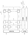
本実施形態による撮像装置100は、図1に示すように、画素アレイ部10と、垂直走査回路20と、列増幅回路30と、水平走査回路40と、制御回路50と、出力回路60とを有している。
As shown in FIG. 1, the
画素アレイ部10には、複数行及び複数列に渡って配された複数の画素12が設けられている。それぞれの画素12は、入射光をその光量に応じた電荷に変換する光電変換素子を含む。
The
垂直走査回路20は、それぞれの画素12から信号を読み出す際に画素12内の読み出し回路を駆動するための制御信号を供給するものである。列増幅回路30は、画素12から読み出された信号に対して増幅処理や必要に応じてAD変換処理等の所定の信号処理を実施する回路部である。水平走査回路40は、列増幅回路30において処理された信号を列毎に順次、出力回路60に転送するためのものである。制御回路50は、垂直走査回路20、列増幅回路30及び水平走査回路40の動作やそのタイミングを制御するためのものである。出力回路60は、画素12から読み出した信号を外部に出力するための回路である。
The
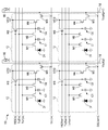
図2は、画素アレイ部10を構成する画素回路の一例を示す回路図である。図2には、画素アレイ部10を構成する画素12として、2行×2列に配列された4個の画素12を示しているが、実際には更に多くの画素12を有している。
FIG. 2 is a circuit diagram illustrating an example of a pixel circuit constituting the
各画素12は、光電変換部D1と、転送トランジスタM1と、転送トランジスタM2と、リセットトランジスタM3と、増幅トランジスタM4と、選択トランジスタM5とを含む。光電変換部D1を構成するフォトダイオードのアノードは接地電圧線に接続され、カソードは転送トランジスタM1のソースに接続されている。転送トランジスタM1のドレインは、転送トランジスタM2のソースに接続されている。転送トランジスタM1のドレインと転送トランジスタM2のソースとの接続ノードは、電荷の保持部C1を構成する。図には、保持部C1を容量素子で表している。転送トランジスタM2のドレインは、リセットトランジスタM3のソース及び増幅トランジスタM4のゲートに接続されている。転送トランジスタM2のドレイン、リセットトランジスタM3のソース及び増幅トランジスタM4のゲートの接続ノードは、電荷の保持部C2を構成する。図には、保持部C2を容量素子で表している。なお、保持部C2は、いわゆるフローティングディフュージョン(FD)である。リセットトランジスタM3のドレイン及び増幅トランジスタM4のドレインは、電源電圧線(VDD)に接続されている。増幅トランジスタM4のソースは、選択トランジスタM5のドレインに接続されている。
Each
画素アレイ部10の画素アレイの各行には、行方向(図2において横方向)に延在して、制御線Tx1、制御線Tx2、制御線RES、制御線SELが、それぞれ配されている。制御線Tx1は、行方向に並ぶ画素12の転送トランジスタM1のゲートにそれぞれ接続され、これら画素12に共通の信号線をなしている。制御線Tx2は、行方向に並ぶ画素12の転送トランジスタM2のゲートにそれぞれ接続され、これら画素12に共通の信号線をなしている。制御線RESは、行方向に並ぶ画素12のリセットトランジスタM3のゲートにそれぞれ接続され、これら画素12に共通の信号線をなしている。制御線SELは、行方向に並ぶ画素12の選択トランジスタM5のゲートにそれぞれ接続され、これら画素12に共通の信号線をなしている。なお、図2には、各制御線の名称に、対応する行番号をそれぞれ付記している(例えば、Tx1(m),Tx1(m+1))。
A control line Tx1, a control line Tx2, a control line RES, and a control line SEL are arranged in each row of the pixel array of the
制御線Tx1、制御線Tx2、制御線RES、制御線SELは、垂直走査回路20に接続されている。制御線Tx1には、垂直走査回路20から、転送トランジスタM1を制御するための駆動パルスである制御信号PTx1が出力される。制御線Tx2には、垂直走査回路20から、転送トランジスタM2を制御するための駆動パルスである制御信号PTx2が出力される。制御線RESには、垂直走査回路20から、リセットトランジスタM3を制御するための駆動パルスである制御信号PRESが出力される。制御線SELには、垂直走査回路20から、選択トランジスタM5を制御するための駆動パルスである制御信号PSELが出力される。典型例では、垂直走査回路20からハイレベルの制御信号が出力されると対応するトランジスタがオンとなり、垂直走査回路20からローレベルの制御信号が出力されると対応するトランジスタがオフとなる。これら制御信号は、制御回路50からの所定のタイミング信号に応じて、垂直走査回路20から供給される。垂直走査回路20には、シフトレジスタやアドレスデコーダなどの論理回路が用いられる。
The control line Tx1, the control line Tx2, the control line RES, and the control line SEL are connected to the
画素アレイ部10の画素アレイの各列には、列方向(図2において縦方向)に延在して、出力線14が配されている。出力線14は、列方向に並ぶ画素12の選択トランジスタM5のソースにそれぞれ接続され、これら画素12に共通の信号線をなしている。なお、画素12の選択トランジスタM5は、省略してもよい。この場合、出力線14は、増幅トランジスタM4のソースに接続される。出力線14には、電流源16が接続されている。
Each column of the pixel array of the
光電変換部D1は、入射光をその光量に応じた電荷に変換(光電変換)するとともに、光電変換により生じた電荷を蓄積する。転送トランジスタM1は、光電変換部D1が保持する電荷を保持部C1に転送する。保持部C1は、光電変換部D1で生成された電荷を、光電変換部D1とは別の場所で保持する。転送トランジスタM2は、保持部C1が保持する電荷を保持部C2に転送する。保持部C2は、保持部C1から転送された電荷を保持するとともに、増幅部の入力ノード(増幅トランジスタM4のゲート)の電圧を、その容量と転送された電荷の量とに応じた電圧に設定する。リセットトランジスタM3は、保持部C2の電圧をリセットする。選択トランジスタM5は、出力線14に信号を出力する画素12を選択する。増幅トランジスタM4は、ドレインに電源電圧が供給され、ソースに選択トランジスタM5を介して電流源16からバイアス電流が供給される構成となっており、ゲートを入力ノードとする増幅部(ソースフォロワ回路)を構成する。これにより増幅トランジスタM4は、入射光によって生じた電荷に基づく信号Voutを、出力線14に出力する。なお、図2には、信号Voutに、対応する列番号をそれぞれ付記している(Vout(p),Vout(p+1))。
The photoelectric conversion unit D1 converts incident light into charges corresponding to the light amount (photoelectric conversion), and accumulates charges generated by the photoelectric conversion. The transfer transistor M1 transfers the charge held by the photoelectric conversion unit D1 to the holding unit C1. The holding unit C1 holds the electric charge generated by the photoelectric conversion unit D1 at a place different from the photoelectric conversion unit D1. The transfer transistor M2 transfers the charge held by the holding unit C1 to the holding unit C2. The holding unit C2 holds the charge transferred from the holding unit C1, and sets the voltage of the input node (gate of the amplification transistor M4) of the amplification unit to a voltage according to the capacity and the amount of transferred charge. To do. The reset transistor M3 resets the voltage of the holding unit C2. The selection transistor M5 selects the
このような構成により、保持部C1が電荷を保持している間に光電変換部D1で生じた電荷は、光電変換部D1に蓄積することができる。これにより、複数の画素12の間で光電変換の期間が一致するような撮像動作、いわゆるグローバル電子シャッタ動作を行うことが可能となる。なお、電子シャッタとは、入射光によって生じた電荷の蓄積を電気的に制御することである。
With such a configuration, charges generated in the photoelectric conversion unit D1 while the holding unit C1 holds charges can be accumulated in the photoelectric conversion unit D1. Thereby, it is possible to perform a so-called global electronic shutter operation in which the photoelectric conversion periods coincide among the plurality of
次に、本実施形態による撮像装置の駆動方法について、図3乃至図5を用いて説明する。ここでは動画を撮影する場合の撮像動作について説明するが、静止画の撮影を行う場合についても同様に行うことができる。 Next, the driving method of the imaging apparatus according to the present embodiment will be described with reference to FIGS. Here, the imaging operation when shooting a moving image will be described, but the same can be done when shooting a still image.
図3は、時間の経過に伴う撮像装置100の動作状態の遷移を示した模式図であり、図面において左から右に向かう方向が時間軸に対応している。図3には、第nフレーム及び第n+1フレームにおける撮像動作を示している。
FIG. 3 is a schematic diagram showing transition of the operation state of the
ここで、以下の説明の便宜上、1フレーム期間の間に、時間軸方向に沿って順番に、時刻T1,T2,T3,T4を定義するものとする。時刻T1はフレームの開始時刻であり、時刻T4はフレームの終了時刻である。連続する2つのフレームにおいて、前のフレームの時刻T4と後のフレームの時刻T1とは一致する。また、時刻T1と時刻T2との間の期間を第1の期間、時刻T2と時刻T3との間の期間を第2の期間、時刻T3と時刻T4との間の期間を第3の期間と定義するものとする。 Here, for convenience of the following description, it is assumed that the times T1, T2, T3, and T4 are defined in order along the time axis direction during one frame period. Time T1 is the start time of the frame, and time T4 is the end time of the frame. In two consecutive frames, the time T4 of the previous frame coincides with the time T1 of the subsequent frame. Further, the period between time T1 and time T2 is the first period, the period between time T2 and time T3 is the second period, and the period between time T3 and time T4 is the third period. Shall be defined.
1フレーム期間の間における撮像動作には、図3に示すように、第1の露光期間と、第2の露光期間とが含まれる。本実施形態において、第1の露光期間は、第1の期間に対応し、相対的に短い露光期間である。また、第2の露光期間は、第2の期間と第3の期間の合計の期間に対応し、第1の露光期間と比較して相対的に長い露光期間である。第2の露光期間は、第1の露光期間の後に開始される。 As shown in FIG. 3, the imaging operation during one frame period includes a first exposure period and a second exposure period. In the present embodiment, the first exposure period corresponds to the first period and is a relatively short exposure period. The second exposure period corresponds to the total period of the second period and the third period, and is a relatively long exposure period compared to the first exposure period. The second exposure period starts after the first exposure period.
また、1フレーム期間の間における撮像動作には、蓄積期間PD(n,1),PD(n,2)が含まれる。蓄積期間PD(n,1)は、第1の露光期間において、光電変換部D1が電荷を生成或いは蓄積している期間である。蓄積期間PD(n,2)は、第2の露光期間において、光電変換部D1が電荷を生成或いは蓄積している期間である。 Further, the imaging operation during one frame period includes accumulation periods PD (n, 1) and PD (n, 2). The accumulation period PD (n, 1) is a period during which the photoelectric conversion unit D1 generates or accumulates charges in the first exposure period. The accumulation period PD (n, 2) is a period during which the photoelectric conversion unit D1 generates or accumulates charges in the second exposure period.
また、1フレーム期間の間における撮像動作には、保持期間MEM(n−1,2)の一部、保持期間MEM(n,1)及び保持期間MEM(n,2)の一部が含まれる。保持期間MEM(n−1,2)は、前フレーム(図示しない第n−1フレーム)の第2の露光期間に光電変換部D1で生成された電荷を保持部C1が保持している期間である。保持期間MEM(n,1)は、第2の期間に対応し、当該フレーム(第nフレーム)の第1の露光期間に光電変換部D1で生成された電荷を保持部C1が保持している期間である。保持期間MEM(n,2)は、当該フレームの第2の露光期間に光電変換部D1で生成された電荷を保持部C1が保持している期間である。保持期間MEM(n,2)は、当該フレームの第3の期間から次フレーム(第n+1フレーム)の第1の期間までの期間に対応する。 The imaging operation during one frame period includes a part of the holding period MEM (n−1, 2), a part of the holding period MEM (n, 1), and a part of the holding period MEM (n, 2). . The holding period MEM (n−1, 2) is a period in which the holding unit C1 holds the charge generated by the photoelectric conversion unit D1 during the second exposure period of the previous frame (n−1 frame not shown). is there. The holding period MEM (n, 1) corresponds to the second period, and the holding unit C1 holds the charge generated by the photoelectric conversion unit D1 during the first exposure period of the frame (nth frame). It is a period. The holding period MEM (n, 2) is a period in which the holding unit C1 holds the charge generated by the photoelectric conversion unit D1 during the second exposure period of the frame. The holding period MEM (n, 2) corresponds to a period from the third period of the frame to the first period of the next frame (n + 1 frame).
また、1フレーム期間の間における撮像動作には、第1の読み出し期間と、第2の読み出し期間とが含まれる。第1の露光期間に蓄積された電荷に基づく信号の読み出し動作を実施する期間が第1の読み出し期間であり、第2の露光期間に蓄積された電荷に基づく信号の読み出し動作を実施する期間が第2の読み出し期間である。第1の読み出し期間は当該フレームの第2の期間内に行われ、第2の読み出し期間は次フレームの第1の期間内に行われる。図には、1行の画素12から一連の読み出し動作を実施する期間を1つの四角印で示している。異なる行の画素12からの読み出し期間を異なる高さの位置に示すことで、行毎に順次読み出し動作が実施されることを模式的に示している。
In addition, the imaging operation during one frame period includes a first readout period and a second readout period. The period for performing the signal readout operation based on the charge accumulated in the first exposure period is the first readout period, and the period for performing the signal readout operation based on the charge accumulated in the second exposure period. This is the second reading period. The first readout period is performed within the second period of the frame, and the second readout period is performed within the first period of the next frame. In the drawing, a period during which a series of reading operations are performed from one row of
なお、図3では、1行目の画素12から順に読み出し動作を行う例を示している。しかし、読み出し動作を行う順序はこの例に限られない。第1の期間及び第2の期間に、1フレームの画像を構成する画素12のそれぞれに対して、少なくとも1回ずつ読み出しが行われればよい。
FIG. 3 shows an example in which the reading operation is sequentially performed from the
保持期間MEM(n,1)に保持部C1が保持している電荷は、第2の期間内において行順次で保持部C2へ転送され、読み出し動作が順次実施される(第1の読み出し)。保持期間MEM(n,2)に保持部C1が保持している電荷は、次フレームの第1の期間内において行順次で保持部C2へ転送され、読み出し動作が順次実施される(第2の読み出し)。なお、第1の読み出し及び第2の読み出しは、必ずしも画素アレイ部10を構成する総ての画素12について実施する必要はなく、一部の画素12についてのみ読み出しを実施してもよい。
The charges held in the holding unit C1 in the holding period MEM (n, 1) are transferred to the holding unit C2 in the row order in the second period, and the reading operation is sequentially performed (first reading). The charges held in the holding unit C1 in the holding period MEM (n, 2) are transferred to the holding unit C2 in the row order in the first period of the next frame, and the reading operation is sequentially performed (second operation). reading). Note that the first readout and the second readout do not necessarily have to be performed for all the
このように、1フレーム期間内の撮像動作には、第1の露光期間に対応する相対的に短い蓄積期間と、第2の露光期間に対応する相対的に長い蓄積期間とが含まれる。短い蓄積期間は、第1の期間に相当する。また、長い蓄積期間は、第2の期間と第3の期間との合計の期間に相当する。或いは、第1の期間の信号の読み出しを終えた後、増幅部の入力ノードをリセットする動作を行わないことにより、長い蓄積期間は、第1の期間と第2の期間と第3の期間との合計の期間とすることもできる。すなわち、第1の期間で生じた電荷と、第2の期間及び第3の期間で生じた電荷とを、増幅部の入力ノードの上で加算することになる。長い蓄積期間は、用途や撮影状況に応じて適宜選択することができる。 Thus, the imaging operation within one frame period includes a relatively short accumulation period corresponding to the first exposure period and a relatively long accumulation period corresponding to the second exposure period. The short accumulation period corresponds to the first period. Further, the long accumulation period corresponds to a total period of the second period and the third period. Alternatively, by not performing the operation of resetting the input node of the amplifying portion after the signal reading in the first period is completed, the long accumulation period can include the first period, the second period, and the third period. It is also possible to set the total period. That is, the charge generated in the first period and the charge generated in the second period and the third period are added on the input node of the amplifying unit. The long accumulation period can be appropriately selected according to the application and the shooting situation.
前フレームの第2の露光期間において蓄積された電荷に基づく信号は、第1の期間に読み出される。そのため、第1の期間が終われば、保持部C1は新たな電荷を保持することができる。また、第1の露光期間において蓄積された電荷に基づく信号は、第2の期間に読み出される。そのため、第2の期間が終われば、保持部C1は新たな電荷を保持することができる。したがって、光電変換部D1は、少なくとも、第1の期間の間に生じる電荷及び第2の期間に生じる電荷のうち多い方の電荷を蓄積できればよい。通常は、第1の期間及び第2の期間に生じる電荷の量は、1フレームの露光期間、すなわち第1の期間と第2の期間と第3の期間との合計の期間に生じる電荷の量より少ないため、光電変換部D1の飽和電荷量を小さくすることができる。 A signal based on the charge accumulated in the second exposure period of the previous frame is read out in the first period. Therefore, when the first period ends, the holding unit C1 can hold a new charge. A signal based on the charge accumulated in the first exposure period is read out in the second period. Therefore, when the second period ends, the holding unit C1 can hold a new charge. Therefore, the photoelectric conversion unit D1 only needs to be able to accumulate at least the larger charge of the charge generated during the first period and the charge generated during the second period. Usually, the amount of charge generated in the first period and the second period is the amount of charge generated in one frame exposure period, that is, the total period of the first period, the second period, and the third period. Therefore, the saturation charge amount of the photoelectric conversion unit D1 can be reduced.
本実施形態の駆動方法では、保持部C1が電荷を保持している第3の期間を、第1の期間及び第2の期間よりも長くしている。そのため、光電変換部D1の飽和電荷量をより小さくすることができる。ただし、第1の期間と第2の期間と第3の期間とは等しくてもよいし、第3の期間よりも第1の期間及び第2の期間が長くてもよい。その他にも任意の蓄積時間の組み合わせをとることができる。 In the driving method of the present embodiment, the third period in which the holding unit C1 holds the charge is longer than the first period and the second period. Therefore, the saturation charge amount of the photoelectric conversion unit D1 can be further reduced. However, the first period, the second period, and the third period may be the same, or the first period and the second period may be longer than the third period. In addition, any combination of accumulation times can be taken.
このように、本実施形態による撮像装置100の駆動方法では、第1の期間及び第2の期間において読み出し動作が行われる。これにより、1フレームの読み出し動作において、1つの画素12から、短い蓄積期間の間に生じた電荷に基づく信号(短い蓄積期間の信号)の読み出しと、長い蓄積期間の間に生じた電荷に基づく信号(長い蓄積期間の信号)の読み出しとが可能になる。これら蓄積時間の異なる信号は、例えば、長い蓄積時間の信号を高感度信号に、短い蓄積時間の信号を低感度信号に、それぞれ対応させることができる。したがって、これら信号を合成することにより、グローバル電子シャッタを行いながら、ワイドダイナミックレンジ画像を得ることができる。
As described above, in the driving method of the
また、図3の読み出し動作では、1フレームの露光が終了してからすぐに、次のフレームの露光を開始することができる。したがって、情報が欠落する期間をほとんどなくすことができるため、画質を向上することができる。 In the read operation of FIG. 3, the exposure of the next frame can be started immediately after the exposure of one frame is completed. Therefore, since the period during which information is lost can be almost eliminated, the image quality can be improved.
また、光電変換部D1が電荷を蓄積している第1の期間及び第2の期間に、複数の画素12のそれぞれに対して読み出し動作が行われる。このため、光電変換部D1の飽和電荷量が小さくても、画素12の飽和電荷量を増加することができる。画素12の飽和電荷量は、1回の露光で生じる電荷のうち、信号として扱うことができる電荷量の最大値である。なお、光電変換部D1の飽和電荷量及び保持部C1の飽和電荷量は、それぞれ、光電変換部D1が蓄積できる電荷量の最大値及び保持部C1が保持できる電荷量の最大値である。
In addition, a readout operation is performed on each of the plurality of
第1の期間及び第2の期間のそれぞれに対する第1の期間と第2の期間と第3の期間との合計の期間の比と、光電変換部D1の飽和電荷量に対する保持部C1の飽和電荷量の比とは、ほぼ等しいことが好ましい。ここで、第1の期間と第2の期間と第3の期間との合計の期間は、1フレームの露光期間のことである。また、低感度信号に対応する露光期間と高感度信号に対応する露光期間の合計でもある。 The ratio of the total period of the first period, the second period, and the third period with respect to each of the first period and the second period, and the saturated charge of the holding unit C1 with respect to the saturated charge amount of the photoelectric conversion unit D1 It is preferable that the ratio of the amounts is approximately equal. Here, the total period of the first period, the second period, and the third period is an exposure period of one frame. It is also the sum of the exposure period corresponding to the low sensitivity signal and the exposure period corresponding to the high sensitivity signal.
本実施形態では、第1の期間に対する1フレームの露光期間の比は4である。また、第1の期間と第2の期間は同じ長さである。つまり、第1の期間は、1フレームの露光期間の1/4である。例えば、毎秒60フレームの動画を撮影する場合、第1の期間は1/240秒である。 In the present embodiment, the ratio of the exposure period of one frame to the first period is 4. Further, the first period and the second period have the same length. That is, the first period is 1/4 of the exposure period of one frame. For example, when shooting a moving image of 60 frames per second, the first period is 1/240 seconds.
そのため、光電変換部D1の飽和電荷量に対する、保持部C1の飽和電荷量の比は4に近いことが好ましい。これは、保持部C1は1回の露光期間で生じた電荷の全部を保持するのに対し、光電変換部D1はその1/4の量の電荷を保持すればよいからである。このような飽和電荷量の比とすることで、光電変換部D1と保持部C1のサイズを最適化することができる。 Therefore, the ratio of the saturation charge amount of the holding unit C1 to the saturation charge amount of the photoelectric conversion unit D1 is preferably close to 4. This is because the holding unit C1 holds all of the charges generated in one exposure period, whereas the photoelectric conversion unit D1 only needs to hold the ¼ amount of charges. By setting such a ratio of the saturated charge amounts, the sizes of the photoelectric conversion unit D1 and the holding unit C1 can be optimized.
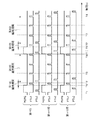
図4は、本実施形態による撮像装置の駆動に用いられる駆動パルスの一例を模式的に示したものである。図4には、第m行目〜第m+2行目の画素12の、転送トランジスタM1の制御線Tx1に供給される制御信号PTx1と、転送トランジスタM2の制御線Tx2に供給される制御信号PTx2とを示している。制御信号がハイレベルのときに対応するトランジスタがオンになり、制御信号がローレベルのときに対応するトランジスタがオフになる。
FIG. 4 schematically shows an example of drive pulses used for driving the imaging apparatus according to the present embodiment. In FIG. 4, the control signal PTx1 supplied to the control line Tx1 of the transfer transistor M1 and the control signal PTx2 supplied to the control line Tx2 of the transfer transistor M2 of the
時刻T1までの期間には、前フレームの露光(第2の露光期間)が行われている。露光とは、光電変換によって生じた電荷が信号として蓄積又は保持されることを意味する。時刻T1より前に生じた前フレームの電荷は、光電変換部D1及び保持部C1に保持されている。制御信号PTx1をハイレベルとして転送トランジスタM1をオンにすることで、前フレームの第2の露光期間に生じた電荷は、総て保持部C1に転送される。時刻T1において制御信号PTx1をローレベルとして総ての画素12で同時に転送トランジスタM1をオフにすることで、前フレームの第2の露光期間は終了する。
During the period up to time T1, exposure of the previous frame (second exposure period) is performed. Exposure means that charges generated by photoelectric conversion are accumulated or held as a signal. The charge of the previous frame generated before time T1 is held in the photoelectric conversion unit D1 and the holding unit C1. By setting the control signal PTx1 to the high level and turning on the transfer transistor M1, all charges generated in the second exposure period of the previous frame are transferred to the holding unit C1. At time T1, the control signal PTx1 is set to the low level, and the transfer transistors M1 are turned off simultaneously in all the
光電変換部D1に蓄積されていた前フレームの電荷が総て保持部C1に転送されると、光電変換部D1は初期状態になる。すなわち、時刻T1において、総ての行の画素12(図4では3行の画素12)の光電変換部D1が同時に電荷の蓄積を新たに開始する。このように、本実施形態の駆動方法では、転送トランジスタM1をオフにすることで、光電変換部D1による電荷の蓄積が開始される。時刻T1は、第1の露光期間の開始時刻となる。
When all the charges of the previous frame accumulated in the photoelectric conversion unit D1 are transferred to the holding unit C1, the photoelectric conversion unit D1 enters an initial state. That is, at time T1, the photoelectric conversion units D1 of all the rows of pixels 12 (three rows of
時刻T1までの間に保持部C1へと転送された電荷に基づく前フレームの信号は、時刻T1以降、順次読み出される(前フレームの第2の読み出し)。すなわち、制御信号PTx2をハイレベルとして転送トランジスタM2をオンにすることで、保持部C1に保持されている電荷を保持部C2に転送する。これにより、保持部C2の容量と転送された電荷の量とに応じて増幅部の入力ノード(増幅トランジスタM4のゲート)の電圧が変化し、出力線14には入力ノードの電圧に基づく信号が出力される。
The signals of the previous frame based on the charges transferred to the holding unit C1 until time T1 are sequentially read after time T1 (second reading of the previous frame). That is, by setting the control signal PTx2 to the high level and turning on the transfer transistor M2, the charge held in the holding unit C1 is transferred to the holding unit C2. As a result, the voltage of the input node of the amplifier (the gate of the amplifier transistor M4) changes according to the capacity of the holding unit C2 and the amount of charge transferred, and a signal based on the voltage of the input node is output to the
この動作を、読み出し対象の画素12について、第1行目から最後の行まで行毎に順次、実施する。図4に示す第m行目から第m+2行目までの動作で説明すると、まず、第m行目の画素12の転送トランジスタM2をオンにすることで、第m行目の画素12の保持部C1の電荷を保持部C2に転送する。これにより、保持部C2の容量及び転送された電荷の量に応じて入力ノードの電圧が変化し、入力ノードの電圧に基づく信号が増幅トランジスタM4によって出力線14に出力される。次いで、第m+1行目の画素12について同様の動作を行い、その後、第m+2行目の画素12について同様の動作を行う。読み出し対象の画素12の読み出しが総て行われた後には、これら画素12の転送トランジスタM1,M2はオフになっている。
This operation is sequentially performed for each pixel from the first row to the last row for the
第1の期間に出力する信号の数は、出力する画像のフォーマット等に応じて適宜変更されうる。例えば、動画の撮影であれば、1フレームに用いられる水平ラインに対応する数の行の画素12から信号が出力されればよい。このような実施形態では、必ずしも撮像装置100が備える総ての画素12から信号が出力されなくてもよい。
The number of signals output in the first period can be changed as appropriate according to the format of the image to be output. For example, in the case of moving image shooting, signals may be output from the
転送トランジスタM1は、時刻T1から、少なくとも前フレームの第2の読み出しが終了するまで、オフ状態に維持される。本実施形態では、総ての画素12の転送トランジスタM1をオフ状態に維持する例を示すが、少なくとも1つの画素12の転送トランジスタM1をオフ状態に維持すればよい。これにより、転送トランジスタM1をオフ状態で維持した画素12においては、この期間に生じた電荷が光電変換部D1に蓄積される。この期間に生じた電荷は光電変換部D1に蓄積されるので、転送トランジスタM1がオフ状態の間、保持部C1は、時刻T1よりも前に生じた電荷を保持することができる。
The transfer transistor M1 is maintained in the off state from time T1 until at least the second reading of the previous frame is completed. In the present embodiment, an example is shown in which the transfer transistors M1 of all the
次いで、前フレームの第2の読み出しが終了後、制御信号PTx1をハイレベルとして転送トランジスタM1をオンにすることで、時刻T1以降に光電変換部D1で生じた電荷を保持部C1に転送する。転送トランジスタM1をオンにしている間に生じる電荷は、光電変換部D1から保持部C1へと即座に転送される。なお、本実施形態では、読み出し対象の総ての画素12の転送トランジスタM1を同時にオフからオンに遷移する例を示している。しかしながら、転送トランジスタM1は時刻T2までにオンになっていればよく、遷移のタイミングは行毎に互いに異なっていてもよい。例えば、前フレームの第2の読み出し動作が終了した行の画素12から順に、転送トランジスタM1をオンにしてもよい。
Next, after the second reading of the previous frame is completed, the control signal PTx1 is set to the high level to turn on the transfer transistor M1, thereby transferring the charge generated in the photoelectric conversion unit D1 after time T1 to the holding unit C1. The charges generated while the transfer transistor M1 is turned on are immediately transferred from the photoelectric conversion unit D1 to the holding unit C1. In the present embodiment, an example is shown in which the transfer transistors M1 of all the
時刻T2において、制御信号PTx1をローレベルとして転送トランジスタM1を同時にオフし、第1の露光期間を終了する。時刻T2は、第1の露光期間の終了時刻となる。光電変換部D1に保持されていた電荷が総て保持部C1に転送されると、光電変換部D1は初期状態になる。すなわち、時刻T2において、総ての画素12の光電変換部D1が同時に電荷の蓄積を新たに開始する。時刻T2は、第2の露光期間の開始時刻となる。時刻T1から時刻T2までの期間が、第1の期間である。第1の露光期間に生じた電荷は、時刻T2以降、保持部C1によって保持される。時刻T2以降に生じた電荷は光電変換部D1に蓄積されるので、転送トランジスタM1がオフ状態の間、保持部C1は、第1の露光期間に生じた電荷を保持することができる。
At time T2, the control signal PTx1 is set to the low level to simultaneously turn off the transfer transistor M1, and the first exposure period ends. Time T2 is the end time of the first exposure period. When all the charges held in the photoelectric conversion unit D1 are transferred to the holding unit C1, the photoelectric conversion unit D1 enters an initial state. That is, at time T2, the photoelectric conversion units D1 of all the
時刻T2までの間に保持部C1へと転送された電荷に基づく信号は、時刻T2以降、順次読み出される(第1の読み出し)。すなわち、前フレームの第2の読み出しと同様に、制御信号PTx2をハイレベルとして転送トランジスタM2をオンにすることで、保持部C1に保持されている電荷を保持部C2に転送する。これにより、保持部C2の容量と転送された電荷の量に応じて増幅部の入力ノード(増幅トランジスタM4のゲート)の電圧が変化し、出力線14には入力ノードの電圧に基づく信号が出力される。
Signals based on the charges transferred to the holding unit C1 until time T2 are sequentially read after time T2 (first reading). That is, as in the second reading of the previous frame, the charge held in the holding unit C1 is transferred to the holding unit C2 by setting the control signal PTx2 to the high level and turning on the transfer transistor M2. As a result, the voltage of the input node of the amplifier (the gate of the amplifier transistor M4) changes according to the capacity of the holding unit C2 and the amount of transferred charge, and a signal based on the voltage of the input node is output to the
この動作を、読み出し対象の画素12について、第1行目から最後の行まで行毎に順次、実行する。図4に示す第m行目から第m+2行目までの動作で説明すると、まず、第m行目の画素12の転送トランジスタM2をオンにすることで、第m行目の画素12の保持部C1の電荷を保持部C2に転送する。これにより、保持部C2の容量と転送された電荷の量に応じて増幅部の入力ノード(増幅トランジスタM4のゲート)の電圧が変化し、入力ノードの電圧に基づく信号が増幅トランジスタM4によって出力線14に出力される。次いで、第m+1行目の画素12について同様の動作を行い、その後、第m+2行目の画素12について同様の動作を行う。読み出し対象の画素12の読み出しが総て行われた後には、これら画素12の転送トランジスタM1,M2はオフになっている。
This operation is sequentially executed for each pixel from the first row to the last row for the
このようにすることで、第1の露光期間の間に蓄積された電荷に基づく信号を、短い蓄積期間の信号(低感度信号)として出力することができる。 In this way, a signal based on the charge accumulated during the first exposure period can be output as a short accumulation period signal (low sensitivity signal).
転送トランジスタM1は、時刻T2から、少なくとも第1の読み出しが終了するまで、オフ状態に維持される。時刻T2以降、転送トランジスタM1が最初にオンになるまでの期間において光電変換部D1で生じた電荷は、光電変換部D1に蓄積される。 The transfer transistor M1 is maintained in the off state from time T2 until at least the first reading is completed. After time T2, the charge generated in the photoelectric conversion unit D1 in a period until the transfer transistor M1 is first turned on is accumulated in the photoelectric conversion unit D1.
第1の読み出しが終了した後、制御信号PTx1をハイレベルとして転送トランジスタM1をオンにすることで、時刻T2以降に光電変換部D1で生じた電荷を保持部C1に転送する。本実施形態の例では、図4に示すように、第1の読み出しの終了後、間欠的に3回、転送トランジスタM1をオンにしている。ここで、1回目の間欠駆動における制御信号PTx1の立ち下がりのタイミングが時刻T3であり、3回目の間欠駆動における制御信号PTx1の立ち下がりのタイミングが時刻T4である。また、時刻T2から時刻T3までの期間が第2の期間であり、時刻T3から時刻T4までの期間が第3の期間である。この場合、1回目の間欠駆動において、第2の期間の間に光電変換部D1に蓄積された電荷が、保持部C1に転送される。以後の間欠駆動においても光電変換部D1から保持部C1への電荷の転送が同様に行われ、3回目の間欠駆動の後の時刻T4には、第2の期間及び第3の期間において光電変換部D1で生じた電荷の総てが保持部C1へ転送されることになる。 After the first reading is completed, the control signal PTx1 is set to the high level to turn on the transfer transistor M1, thereby transferring the charge generated in the photoelectric conversion unit D1 after the time T2 to the holding unit C1. In the example of this embodiment, as shown in FIG. 4, the transfer transistor M1 is turned on three times intermittently after the end of the first reading. Here, the fall timing of the control signal PTx1 in the first intermittent drive is time T3, and the fall timing of the control signal PTx1 in the third intermittent drive is time T4. The period from time T2 to time T3 is the second period, and the period from time T3 to time T4 is the third period. In this case, in the first intermittent drive, the charge accumulated in the photoelectric conversion unit D1 during the second period is transferred to the holding unit C1. In subsequent intermittent driving, charge transfer from the photoelectric conversion unit D1 to the holding unit C1 is performed in the same manner, and at time T4 after the third intermittent driving, photoelectric conversion is performed in the second period and the third period. All the charges generated in the part D1 are transferred to the holding part C1.
転送トランジスタM1を間欠的に駆動しているのは、第2の露光期間の間に生成される電荷が光電変換部D1の飽和電荷量を超える前に保持部C1へと転送するためである。間欠動作を行う間隔は、光電変換部D1の飽和電荷量等に応じて適宜選択することができるが、一実施例では、第1の期間或いは第2の期間と同じ長さに設定することができる。間欠動作を行う間隔は、均等であることが望ましい。 The reason why the transfer transistor M1 is intermittently driven is that the charge generated during the second exposure period is transferred to the holding unit C1 before it exceeds the saturation charge amount of the photoelectric conversion unit D1. The interval at which the intermittent operation is performed can be appropriately selected according to the saturation charge amount of the photoelectric conversion unit D1 or the like. However, in one embodiment, the interval may be set to the same length as the first period or the second period. it can. It is desirable that the intervals at which the intermittent operation is performed be uniform.
なお、時刻T2から時刻T4の間において、光電変換部D1から保持部C1に電荷を転送する期間は、第1の読み出しが終了した後であれば、自由に設定することができる。例えば、転送トランジスタM1を間欠的にオンする回数は、3回に限定されるものではなく、何度でもよい。また、転送トランジスタM1は、第3の期間の間、常にオン状態に維持していてもよい。その場合には、第3の期間に生じた電荷は、光電変換部D1から即座に保持部C1に転送される。ただし、ノイズを低減する観点からは、転送トランジスタM1をオンにする期間が短い動作、例えば上述の間欠動作が望ましい。 Note that the period during which charge is transferred from the photoelectric conversion unit D1 to the holding unit C1 between time T2 and time T4 can be freely set as long as the first reading is completed. For example, the number of times the transfer transistor M1 is intermittently turned on is not limited to three, and may be any number. Further, the transfer transistor M1 may always be kept on during the third period. In that case, the charge generated in the third period is immediately transferred from the photoelectric conversion unit D1 to the holding unit C1. However, from the viewpoint of reducing noise, an operation with a short period during which the transfer transistor M1 is turned on, for example, the above-described intermittent operation is desirable.
次いで、時刻T4において、総ての行の制御信号PTx1をハイレベルからローレベルへと遷移することにより、総ての行の画素12の転送トランジスタM1を同時にオンからオフに制御する。これにより、1フレームの露光期間が終了する。時刻T4は、第2の露光期間の終了時刻となる。
Next, at time T4, the control signals PTx1 for all the rows are changed from the high level to the low level, thereby simultaneously controlling the transfer transistors M1 of the
次いで、次の第n+1フレームの第1の期間において、前述した前フレームの第2の読み出しと同様にして、第nフレームの第2の露光期間に生じた電荷に基づく信号の読み出しを行う(第2の読み出し)。 Next, in the first period of the next (n + 1) th frame, in the same manner as the second reading of the previous frame described above, a signal is read based on the charge generated in the second exposure period of the nth frame (the first frame). 2).
このようにすることで、第2の露光期間の間に蓄積された電荷に基づく信号を、長い蓄積期間の信号(高感度信号)として出力することができる。 By doing so, a signal based on the charge accumulated during the second exposure period can be output as a signal (high sensitivity signal) of a long accumulation period.
このように、本実施形態による撮像装置の駆動方法では、総ての画素12において、露光期間が互いに一致している。つまり、総ての画素12において、時刻T1に露光が開始し、時刻T4に露光が終了する。また、時刻T4において、次フレームの露光が開始され、以降、時刻T1から時刻T4までの動作が繰り返される。
As described above, in the driving method of the imaging apparatus according to the present embodiment, the exposure periods of all the
このようにして得られた蓄積期間の異なる低感度信号と高感度信号とを合成することにより、ダイナミックレンジを拡大することができる。これにより、撮影される画像において被写体の黒つぶれや白飛びを回避することが可能となり、高品質な画像を得ることができる。 The dynamic range can be expanded by synthesizing the low-sensitivity signal and the high-sensitivity signal obtained in this manner and having different accumulation periods. As a result, it is possible to avoid blackout and whiteout of the subject in the captured image, and a high-quality image can be obtained.
次に、1つの画素12からの信号の読み出し動作について、図5を用いて説明する。図5は、本実施形態による撮像装置100の駆動に用いられる駆動パルスの一例を模式的に示したものである。図5には、選択トランジスタM5に供給される制御信号PSELと、リセットトランジスタM3に供給される制御信号PRESと、転送トランジスタM2に供給される制御信号PTx2とを示している。制御信号がハイレベルのときに対応するトランジスタがオンとなり、制御信号がローレベルのときに対応するトランジスタがオフとなる。
Next, a signal reading operation from one
図5(a)は、第2の読み出しにおいて、第2の露光期間の蓄積電荷に対応する信号を読み出す場合のタイミングチャートである。図5(b)は、第2の読み出しにおいて、第1の露光期間及び第2の露光期間の蓄積電荷に対応する信号を読み出す場合のタイミングチャートである。各図において、破断線よりも左側が第1の読み出しの動作を示し、破断線よりも右側が第2の読み出しの動作を示している。 FIG. 5A is a timing chart in the case where a signal corresponding to the accumulated charge in the second exposure period is read in the second reading. FIG. 5B is a timing chart in the case where a signal corresponding to the accumulated charge in the first exposure period and the second exposure period is read in the second reading. In each figure, the left side of the broken line shows the first reading operation, and the right side of the broken line shows the second reading operation.
第1の読み出し動作では、図5(a),(b)に示される駆動パルスに従って、画素12の選択、リセット、ノイズ信号の読み出し(N読み)、電荷の転送、光信号の読み出し(S読み)が行われる。
In the first readout operation, the
図5(a)に示される第2の読み出し動作では、第1の読み出し動作と同様に、画素12の選択、リセット、ノイズ信号の読み出し(N読み)、電荷の転送、光信号の読み出し(S読み)が、順次行われる。図5(a)の動作では、電荷の転送(PTx2)の前に保持部C2のリセット(PRES)を行っているため、保持部C1からの電荷の転送の後に保持部C2が保持する電荷は、第2の露光期間において生じた電荷のみとなる。なお、上述した図4の説明は、図5(a)の読み出し動作を前提としている。
In the second readout operation shown in FIG. 5A, as in the first readout operation, the
図5(b)に示される第2の読み出し動作では、画素12の選択、電荷の転送、光信号の読み出し(S読み)が、順次行われる。すなわち、第2の読み出しの際には、電荷の転送の前に保持部C2のリセットは行わない。図5(b)の動作では電荷の転送前にリセットを行わないため、保持部C1からの電荷の転送前の保持部C2には、第1の露光期間において生じた電荷が残存している。したがって、この状態で第2の露光期間において生じた電荷を保持部C1から保持部C2へ転送すると、保持部C2には、第1の露光期間において生じた電荷と、第2の露光期間において生じた電荷とが転送されることになる。つまり、図5(b)に示される第2の読み出しは、第1の露光期間及び第2の露光期間の蓄積電荷に対応する信号を読み出すことに相当する。
In the second readout operation shown in FIG. 5B, the selection of the
このようにして画素12から出力された信号は、撮像装置100の内部(例えば、AD変換機能を備えた列増幅回路30)でAD変換されてもよいし、撮像装置100の外部(例えば、後述する信号処理部208)でAD変換されてもよい。
The signals output from the
以上、説明したように、本実施形態による撮像装置の駆動方法を用いることにより、短い蓄積時間の信号と長い蓄積時間の信号とを、同じフレーム期間において取得することができる。したがって、これらの信号から得られる画像を用いることで、ダイナミックレンジを拡大した画像を得ることができる。 As described above, by using the driving method of the imaging apparatus according to the present embodiment, a signal having a short accumulation time and a signal having a long accumulation time can be acquired in the same frame period. Therefore, an image with an expanded dynamic range can be obtained by using images obtained from these signals.
また、長い蓄積時間の信号として、第1の露光期間及び第2の露光期間の蓄積電荷に基づく信号を用いることで、短い蓄積時間の信号の露光期間と長い蓄積時間の信号の露光期間とは、どちらも時刻T1において開始されることになる。また、これら露光期間は、重複する露光期間(第1の期間)を有する。このように露光期間の開始時刻を揃えることにより、短い蓄積時間の信号に基づく画像と長い蓄積時間の信号に基づく画像とを合成する際の被写体の位置ずれを低減することができる。これにより、被写体の位置ずれが小さく、黒つぶれや白飛びのないワイドダイナミックレンジ画像を得ることができる。 In addition, by using a signal based on the accumulated charge in the first exposure period and the second exposure period as the long accumulation time signal, the exposure period of the short accumulation time signal and the exposure period of the long accumulation time signal Both are started at time T1. Further, these exposure periods have overlapping exposure periods (first periods). By aligning the start times of the exposure periods in this way, it is possible to reduce the positional deviation of the subject when the image based on the short accumulation time signal and the image based on the long accumulation time signal are combined. Thereby, it is possible to obtain a wide dynamic range image in which the subject position is small and no blackout or whiteout occurs.
画素12の光電変換部D1は、少なくとも第1の期間或いは第2の期間に生じる電荷を蓄積できればよいため、光電変換部D1の飽和電荷量が小さくても、画素12の飽和電荷量を維持することができる。したがって、このような構成により、画素12の飽和電荷量を維持しつつ、グローバル電子シャッタを行いながら、ワイドダイナミックレンジ画像を得ることができる。なお、画素12の保持部C1が電荷を保持している第3の期間は、第1の期間及び第2の期間よりも長いことが望ましい。このようにすることで、光電変換部D1の飽和電荷量をより小さくすることができる。
Since the photoelectric conversion unit D1 of the
本実施形態では、所定のフレームにおいて、短い蓄積期間の撮像後に、長い蓄積期間の撮像を行う例を説明した。しかし、所定のフレームにおいて、長い蓄積期間の撮像の後に短い蓄積期間の撮像を行ってもよい。 In the present embodiment, an example in which imaging for a long accumulation period is performed after imaging for a short accumulation period in a predetermined frame has been described. However, in a predetermined frame, imaging in a short accumulation period may be performed after imaging in a long accumulation period.
また、本実施形態の撮像装置100は、ローリングシャッタ動作を行う動作モードを有していてもよい。ローリングシャッタ動作を行う動作モードでは、複数の画素12の光電変換部D1による電荷の蓄積を、順次、開始する。その後、複数の画素12の転送トランジスタM1を、順次、オンに制御する。また、本実施形態の撮像装置100は、別の方式のグローバル電子シャッタを行う動作モードを有していてもよい。別の方式のグローバル電子シャッタとは、光電変換部D1が電荷を蓄積している期間が露光期間と等しくなるような動作である。
Further, the
このように、本実施形態によれば、画素の飽和を抑制しつつ、グローバル電子シャッタ動作を行うことができる。また、ダイナミックレンジを拡大した画像を得ることができる。 Thus, according to the present embodiment, it is possible to perform a global electronic shutter operation while suppressing pixel saturation. In addition, an image with an expanded dynamic range can be obtained.
[第2実施形態]
本発明の第2実施形態による撮像装置について、図6乃至図8を用いて説明する。図1乃至図5に示す第1実施形態による撮像装置と同様の構成要素には同一の符号を付し、説明を省略し或いは簡潔にする。図6は、本実施形態による撮像装置の画素回路の構成例を示す回路図である。図7は、本実施形態による撮像装置の動作を示す模式図である。図8は、本実施形態による撮像装置の動作を示すタイミングチャートである。
[Second Embodiment]
An imaging apparatus according to a second embodiment of the present invention will be described with reference to FIGS. Constituent elements similar to those of the imaging apparatus according to the first embodiment shown in FIGS. 1 to 5 are denoted by the same reference numerals, and description thereof is omitted or simplified. FIG. 6 is a circuit diagram illustrating a configuration example of the pixel circuit of the imaging apparatus according to the present embodiment. FIG. 7 is a schematic diagram illustrating the operation of the imaging apparatus according to the present embodiment. FIG. 8 is a timing chart showing the operation of the imaging apparatus according to the present embodiment.
はじめに、本実施形態による撮像装置100の構成について、図6を用いて説明する。
First, the configuration of the
本実施形態による撮像装置100は、画素12の回路構成が異なるほかは、第1実施形態による撮像装置100と同様である。本実施形態による撮像装置100の画素12は、図6に示すように、光電変換部D1、転送トランジスタM1,M2、リセットトランジスタM3、増幅トランジスタM4、選択トランジスタM5に加え、オーバーフロートランジスタM6を更に有している。
The
オーバーフロートランジスタM6のソースは、光電変換部D1を構成するフォトダイオードのカソードと転送トランジスタM1のソースとの接続ノードに接続されている。オーバーフロートランジスタM6のドレインは、電源電圧線(VDD)に接続されている。画素アレイ部10の画素アレイの各行には、制御線OFGが更に配されている。制御線OFGは、行方向に並ぶ画素12のオーバーフロートランジスタM6のゲートにそれぞれ接続され、これら画素12に共通の信号線をなしている。制御線OFGは、垂直走査回路20に接続されている。制御線OFGには、垂直走査回路20から、オーバーフロートランジスタM6を制御するための制御信号POFGが出力される。典型例では、垂直走査回路20からハイレベルの制御信号POFGが出力されるとオーバーフロートランジスタM6がオンとなり、垂直走査回路20からローレベルの制御信号が出力されるとオーバーフロートランジスタM6がオフとなる。
The source of the overflow transistor M6 is connected to a connection node between the cathode of the photodiode constituting the photoelectric conversion unit D1 and the source of the transfer transistor M1. The drain of the overflow transistor M6 is connected to the power supply voltage line (VDD). A control line OFG is further arranged in each row of the pixel array of the
オーバーフロートランジスタM6は、光電変換部D1の電荷を電源ノードに排出する機能を備える。 The overflow transistor M6 has a function of discharging the charge of the photoelectric conversion unit D1 to the power supply node.
第1実施形態では転送トランジスタM1を制御することによって光電変換部D1における電荷の蓄積を開始したが、本実施形態ではオーバーフロートランジスタM6を制御することによって光電変換部D1における電荷の蓄積を開始することも可能である。具体的には、オーバーフロートランジスタM6をオンからオフへ制御することで、光電変換部D1による電荷の蓄積を開始することができる。これにより、露光時間の設定の自由度を向上することができる。 In the first embodiment, charge accumulation in the photoelectric conversion unit D1 is started by controlling the transfer transistor M1, but in this embodiment, charge accumulation in the photoelectric conversion unit D1 is started by controlling the overflow transistor M6. Is also possible. Specifically, charge accumulation by the photoelectric conversion unit D1 can be started by controlling the overflow transistor M6 from on to off. Thereby, the freedom degree of the setting of exposure time can be improved.
次に、本実施形態による撮像装置の駆動方法について、図7及び図8を用いて説明する。本実施形態による撮像装置の駆動方法は、第1の露光期間の開始時刻をオーバーフロートランジスタM6によって制御している点において、第1実施形態による撮像装置の駆動方法とは異なっている。ここでは、第1実施形態の駆動方法と異なる点を中心に説明し、同じ部分については説明を省略し或いは簡潔にする。 Next, the driving method of the imaging apparatus according to the present embodiment will be described with reference to FIGS. The driving method of the imaging apparatus according to the present embodiment is different from the driving method of the imaging apparatus according to the first embodiment in that the start time of the first exposure period is controlled by the overflow transistor M6. Here, the difference from the driving method of the first embodiment will be mainly described, and the description of the same part will be omitted or simplified.
図7は、時間の経過に伴う撮像装置100の動作状態の遷移を示した模式図であり、図面において左から右に向かう方向が時間軸に対応している。図7には、第nフレーム及び第n+1フレームにおける撮像動作を示している。
FIG. 7 is a schematic diagram showing transition of the operation state of the
本実施形態による撮像装置の駆動方法は、図7に示すように、1フレーム期間の間に、第1の露光期間と、第2の露光期間と、蓄積期間PD(n,1),PD(n,2)と、排出期間OFDとを含む。また、1フレーム期間の間に、保持期間MEM(n−1,2),MEM(n,1),MEM(n,2)と、2回の読み出し期間とを含む。 As shown in FIG. 7, the driving method of the image pickup apparatus according to the present embodiment includes a first exposure period, a second exposure period, an accumulation period PD (n, 1), PD ( n, 2) and the discharge period OFD. Further, one frame period includes a holding period MEM (n-1, 2), MEM (n, 1), MEM (n, 2), and two reading periods.
第1の露光期間は、時刻T1と時刻T2との間の時刻T5から時刻T2までの期間に対応し、相対的に短い露光期間である。第2の露光期間は、第2の期間と第3の期間の合計の期間に対応し、第1の露光期間と比較して相対的に長い露光期間である。第2の露光期間は、第1の露光期間の後に開始される。蓄積期間PD(n,1)は、第1の露光期間において、光電変換部D1が電荷を生成或いは蓄積している期間である。保持期間MEM(n,1)は、第1の露光期間に光電変換部D1で生成された電荷を保持部C1が保持している期間である。蓄積期間PD(n,2)は、第2の露光期間において、光電変換部D1が電荷を生成或いは蓄積している期間である。保持期間MEM(n,2)は、第2の露光期間に光電変換部D1で生成された電荷を保持部C1が保持している期間である。排出期間OFDは、オーバーフロートランジスタM6がオンの期間である。排出期間OFD中に光電変換部D1で生じた電荷或いは光電変換部D1に保持されている電荷は、オーバーフロートランジスタM6を介して排出されるため、光電変換部D1には蓄積されない。 The first exposure period corresponds to a period from time T5 to time T2 between time T1 and time T2, and is a relatively short exposure period. The second exposure period corresponds to the total period of the second period and the third period, and is an exposure period that is relatively longer than the first exposure period. The second exposure period starts after the first exposure period. The accumulation period PD (n, 1) is a period during which the photoelectric conversion unit D1 generates or accumulates charges in the first exposure period. The holding period MEM (n, 1) is a period in which the holding unit C1 holds the charge generated by the photoelectric conversion unit D1 in the first exposure period. The accumulation period PD (n, 2) is a period during which the photoelectric conversion unit D1 generates or accumulates charges in the second exposure period. The holding period MEM (n, 2) is a period in which the holding unit C1 holds the charge generated by the photoelectric conversion unit D1 in the second exposure period. The discharge period OFD is a period in which the overflow transistor M6 is on. The charge generated in the photoelectric conversion unit D1 during the discharge period OFD or the charge held in the photoelectric conversion unit D1 is discharged through the overflow transistor M6 and is not accumulated in the photoelectric conversion unit D1.
本実施形態による撮像装置100の駆動方法では、第1の露光期間が、時刻T1と時刻T2との間の時刻T5から時刻T2までの期間となるように、その開始時刻と終了時刻とを規定している。このような場合、第1の露光期間の開始時刻は、制御信号POFGのタイミングにより制御することができる。また、第1の露光期間の終了時刻は、第1実施形態の場合と同様、制御信号PTx1のタイミングにより制御することができる。
In the driving method of the
より具体的には、第1の露光期間の開始時刻は、フレーム期間の開始後、最初に制御信号POFGがハイレベルからローレベルへと遷移するタイミングによって規定することができる。制御信号POFGをローレベルとしてオーバーフロートランジスタM6をオフにすることで、光電変換部D1で生じた電荷は、オーバーフロートランジスタM6を介して排出されなくなり、光電変換部D1に蓄積されるようになる。 More specifically, the start time of the first exposure period can be defined by the timing at which the control signal POFG first transitions from the high level to the low level after the start of the frame period. By turning off the overflow transistor M6 by setting the control signal POFG to the low level, the charge generated in the photoelectric conversion unit D1 is not discharged through the overflow transistor M6, but is accumulated in the photoelectric conversion unit D1.
また、第1の露光期間の終了時刻は、制御信号POFGがローレベルであって、且つ、制御信号PTx1がハイレベルからローレベルへと遷移するタイミングによって規定することができる。第1の露光期間は、光電変換部D1で生じた電荷を保持部C1に転送することによって終了する。オーバーフロートランジスタM6がオンになると光電変換部D1がリセットされるため、露光期間の終了時刻は、オーバーフロートランジスタM6がオンになるタイミングよりも前に、転送トランジスタM1がオフになるタイミングとなる。露光期間の開始時刻から終了時刻までの間、オーバーフロートランジスタM6はオフ状態のまま維持する。 The end time of the first exposure period can be defined by the timing at which the control signal POFG is at the low level and the control signal PTx1 transitions from the high level to the low level. The first exposure period ends when the charge generated in the photoelectric conversion unit D1 is transferred to the holding unit C1. Since the photoelectric conversion unit D1 is reset when the overflow transistor M6 is turned on, the end time of the exposure period is the timing when the transfer transistor M1 is turned off before the timing when the overflow transistor M6 is turned on. The overflow transistor M6 is maintained in the OFF state from the start time to the end time of the exposure period.
第2の露光期間における撮像動作は、この期間の間、制御信号POFGをローレベルとしてオーバーフロートランジスタM6をオフ状態に維持しているほかは、第1実施形態の場合と同様である。 The imaging operation in the second exposure period is the same as that in the first embodiment except that the control signal POFG is set to the low level and the overflow transistor M6 is maintained in the OFF state during this period.
図8は、本実施形態による撮像装置100の駆動方法に用いられる駆動パルスの一例を模式的に示したものである。図8には、第m行目〜第m+2行目の画素12の、制御線Tx1に供給される制御信号PTx1と、制御線Tx2に供給される制御信号PTx2と、制御線OFGに供給される制御信号POFGとを示している。制御信号がハイレベルのときに対応するトランジスタがオンになり、制御信号がローレベルのときに対応するトランジスタがオフになる。なお、制御信号PTx1,PTx2の駆動タイミングは、第1実施形態による撮像装置100の駆動方法の場合と同じである。
FIG. 8 schematically shows an example of drive pulses used in the method for driving the
時刻T1において、フレーム期間は開始されるが、制御信号POFGはハイレベルでありオーバーフロートランジスタM6がオンになっているため、光電変換部D1で生じた電荷は蓄積されない。第1の露光期間は、制御信号POFGがハイレベルからローレベルへと遷移するタイミング、すなわちオーバーフロートランジスタM6がオフになる時刻T5から開始される。オーバーフロートランジスタM6がオフの間、光電変換部D1で生じた電荷は光電変換部D1に蓄積される。読み出し対象の画素12について同時にオーバーフロートランジスタM6をオフにすることで、グローバル電子シャッタ動作が可能となる。
At time T1, the frame period is started, but the control signal POFG is at the high level and the overflow transistor M6 is turned on, so that the charge generated in the photoelectric conversion unit D1 is not accumulated. The first exposure period starts from the timing when the control signal POFG transitions from the high level to the low level, that is, the time T5 when the overflow transistor M6 is turned off. While the overflow transistor M6 is off, the charge generated in the photoelectric conversion unit D1 is accumulated in the photoelectric conversion unit D1. By simultaneously turning off the overflow transistor M6 for the
オーバーフロートランジスタM6がオンからオフに制御される時刻T5は、図7に示すように、前フレームの信号読み出しを行っている期間にある。すなわち、第1の露光期間は、前フレームの信号読み出しを行っている期間中に開始している。このようにすることで、情報が欠落する期間を短くすることができ、画質を向上することができる。 The time T5 when the overflow transistor M6 is controlled from on to off is in the period during which the signal of the previous frame is being read, as shown in FIG. That is, the first exposure period starts during the period in which the signal of the previous frame is being read. By doing so, the period during which information is lost can be shortened, and the image quality can be improved.
オーバーフロートランジスタM6がオフの期間中に、制御信号PTx1をハイレベルとして転送トランジスタM1をオンにすることで、光電変換部D1で生じた電荷を保持部C1に転送する。本実施形態の例では、図8に示すように、オーバーフロートランジスタM6がオフの間、間欠的に4回、転送トランジスタM1をオンにしている。転送トランジスタM1を間欠的に駆動している理由は、第1実施形態の場合と同様である。 While the overflow transistor M6 is off, the control signal PTx1 is set to the high level to turn on the transfer transistor M1, thereby transferring the charge generated in the photoelectric conversion unit D1 to the holding unit C1. In the example of this embodiment, as shown in FIG. 8, while the overflow transistor M6 is off, the transfer transistor M1 is turned on four times intermittently. The reason why the transfer transistor M1 is driven intermittently is the same as in the first embodiment.
第1の露光期間の終了時刻は、オーバーフロートランジスタM6がオフの状態において、転送トランジスタM1がオフになるタイミングによって規定することができる。図8の例では、転送トランジスタM1の1回目の間欠駆動における制御信号PTx1の立ち下がりのタイミング、すなわち時刻T2を、第1の露光期間の終了時刻としている。このとき、読み出し対象の画素12について同時に転送トランジスタM1をオフにすることで、グローバル電子シャッタ動作が可能となる。つまり、図8の駆動によれば、短い蓄積期間に対応する第1の露光期間は、時刻T5から時刻T2の期間である。
The end time of the first exposure period can be defined by the timing at which the transfer transistor M1 is turned off when the overflow transistor M6 is turned off. In the example of FIG. 8, the falling timing of the control signal PTx1 in the first intermittent drive of the transfer transistor M1, that is, the time T2, is the end time of the first exposure period. At this time, the global electronic shutter operation can be performed by simultaneously turning off the transfer transistor M1 for the
時刻T2までの間に保持部C1へと転送された電荷に基づく信号は、時刻T2以降、転送トランジスタM1の2回目の間欠駆動よりも前の期間(第2の期間)に、順次読み出される(第1の読み出し)。 A signal based on the charge transferred to the holding unit C1 until time T2 is sequentially read out after time T2 in a period (second period) before the second intermittent driving of the transfer transistor M1 (second period) ( First read).
第1の露光期間の終了時刻である時刻T2は、第2の露光期間の開始時刻でもある。第2の露光期間の終了時刻は、図8の例では、転送トランジスタM1の4回目の間欠駆動における制御信号PTx1の立ち下がりのタイミング、すなわち時刻T4となる。第2の露光期間における電荷の蓄積並びに第2の露光期間において生じた電荷に基づく信号の読み出し(第2の読み出し)の動作は、第1実施形態の場合と同様である。オーバーフロートランジスタM6は、第2の露光期間の終了時刻である時刻T4以降にオフからオンへと制御する。 Time T2, which is the end time of the first exposure period, is also the start time of the second exposure period. In the example of FIG. 8, the end time of the second exposure period is the falling timing of the control signal PTx1 in the fourth intermittent drive of the transfer transistor M1, that is, time T4. The operation of accumulating charges in the second exposure period and reading out signals based on the charges generated in the second exposure period (second reading) are the same as in the first embodiment. The overflow transistor M6 controls from off to on after time T4, which is the end time of the second exposure period.
なお、上述の例では、前フレームの第2の読み出し期間の間にオーバーフロートランジスタM6をオンからオフに制御する例を示したが、オーバーフロートランジスタM6をオンからオフに制御するタイミングは、これに限定されるものではない。すなわち、オーバーフロートランジスタM6は、前フレームの第2の読み出し動作の完了と同時にオンからオフに制御してもよいし、前フレームの第2の読み出し動作が完了した後にオフに制御してもよい。これらの場合、オーバーフロートランジスタM6をオフにした時点で保持部C1には前フレームの電荷がないため、転送トランジスタM1をオフからオンに制御することができる。したがって、光電変換部D1に瞬間的に強い光が入射し、光電変換部D1の飽和電荷量を超える電荷が生じた場合でも、光電変換部D1の飽和電荷量と保持部C1の飽和電荷量の合計の飽和電荷量まで、画素12を飽和させずに用いることができる。すなわち、本実施形態によれば、被写体の明るさに応じて、駆動方法を変えることができる。
In the above example, the overflow transistor M6 is controlled from on to off during the second readout period of the previous frame. However, the timing for controlling the overflow transistor M6 from on to off is limited to this. Is not to be done. That is, the overflow transistor M6 may be controlled from on to off simultaneously with the completion of the second read operation of the previous frame, or may be controlled to be off after the second read operation of the previous frame is completed. In these cases, since there is no charge in the previous frame in the holding unit C1 when the overflow transistor M6 is turned off, the transfer transistor M1 can be controlled from off to on. Therefore, even when intense light is incident on the photoelectric conversion unit D1 and charges exceeding the saturation charge amount of the photoelectric conversion unit D1 are generated, the saturation charge amount of the photoelectric conversion unit D1 and the saturation charge amount of the holding unit C1 The
また、低感度信号に対応する第1の露光期間の長さを図8のように短くした場合、高感度信号に対応する第2の露光期間の長さを短くすることができる。これにより、被写体が高速で動く場合などの被写体ブレを小さくすることができる。 Further, when the length of the first exposure period corresponding to the low sensitivity signal is shortened as shown in FIG. 8, the length of the second exposure period corresponding to the high sensitivity signal can be shortened. Thereby, subject blurring when the subject moves at high speed can be reduced.
このように、本実施形態によれば、画素の飽和を抑制しつつ、グローバル電子シャッタ動作を行うことができる。また、ダイナミックレンジを拡大した画像を得ることができる。また、オーバーフロートランジスタを用いることで、露光期間の設定の自由度を向上することができる。これにより、高輝度の被写体に対して、低感度信号に対応する第1の露光期間をごく短く設定することができる。これにより、画素が飽和することなく信号を扱うことが可能となるため、より白トビの少ない高品位な画像を得ることができる。 Thus, according to the present embodiment, it is possible to perform a global electronic shutter operation while suppressing pixel saturation. In addition, an image with an expanded dynamic range can be obtained. Further, by using an overflow transistor, the degree of freedom in setting the exposure period can be improved. As a result, the first exposure period corresponding to the low sensitivity signal can be set very short for a high-luminance subject. As a result, signals can be handled without pixel saturation, and a high-quality image with less white stripes can be obtained.
[第3実施形態]
本発明の第3実施形態による撮像装置について、図9及び図10を用いて説明する。図1乃至図8に示す第1及び第2実施形態による撮像装置と同様の構成要素には同一の符号を付し、説明を省略し或いは簡潔にする。図9は、本実施形態による撮像装置の動作を示す模式図である。図10は、本実施形態による撮像装置の動作を示すタイミングチャートである。
[Third Embodiment]
An imaging apparatus according to a third embodiment of the present invention will be described with reference to FIGS. Constituent elements similar to those of the imaging apparatus according to the first and second embodiments shown in FIGS. 1 to 8 are denoted by the same reference numerals, and description thereof is omitted or simplified. FIG. 9 is a schematic diagram illustrating the operation of the imaging apparatus according to the present embodiment. FIG. 10 is a timing chart showing the operation of the imaging apparatus according to the present embodiment.
本実施形態では、図6に示す回路構成の画素12を有する第2実施形態による撮像装置100の他の駆動方法を説明する。本実施形態による撮像装置100の駆動方法は、第1の露光期間の間に生じた電荷を保持する期間として、光電変換部D1で保持する期間と保持部C1で保持する期間とを有する点で、第2実施形態による撮像装置100の駆動方法とは異なっている。ここでは、第1及び第2実施形態の駆動方法と異なる点を中心に説明し、同様の部分については説明を省略し或いは簡潔にする。
In the present embodiment, another driving method of the
図9は、時間の経過に伴う撮像装置100の動作状態の遷移を示した模式図であり、図面において左から右に向かう方向が時間軸に対応している。図9には、第nフレーム及び第n+1フレームにおける撮像動作を示している。
FIG. 9 is a schematic diagram showing transition of the operation state of the
本実施形態による駆動方法は、第1の露光期間を含む第1の期間において前フレームの信号の読み出しを実施する点は、第1及び第2実施形態の場合と同じである。本実施形態による駆動方法が第1及び第2実施形態と異なる点は、第1の露光期間の途中で光電変換部D1から保持部C1へと電荷を転送している点である。すなわち、本実施形態による駆動方法では、第1の期間中に、転送トランジスタM1をオフからオンへと制御している。図9の模式図で説明すると、第1の露光期間の間に、蓄積期間PD(n,1)と保持期間MEM(n,1)とが重複する期間を有している。 The driving method according to the present embodiment is the same as the first and second embodiments in that the signal of the previous frame is read in the first period including the first exposure period. The driving method according to this embodiment is different from the first and second embodiments in that charges are transferred from the photoelectric conversion unit D1 to the holding unit C1 during the first exposure period. That is, in the driving method according to the present embodiment, the transfer transistor M1 is controlled from OFF to ON during the first period. Referring to the schematic diagram of FIG. 9, the accumulation period PD (n, 1) and the holding period MEM (n, 1) have a period that overlaps during the first exposure period.
図10は、本実施形態による撮像装置100の駆動方法に用いられる駆動パルスの一例を模式的に示したものである。図10には、第m行目〜第m+2行目の画素12の、制御線Tx1に供給される制御信号PTx1と、制御線Tx2に供給される制御信号PTx2と、制御線OFGに供給される制御信号POFGとを示している。制御信号がハイレベルのときに対応するトランジスタがオンになり、制御信号がローレベルのときに対応するトランジスタがオフになる。なお、制御信号POFGの駆動タイミングは、第2実施形態による撮像装置100の駆動方法の場合と同じである。
FIG. 10 schematically shows an example of drive pulses used in the method for driving the
時刻T1において、フレーム期間は開始されるが、制御信号POFGはハイレベルでありオーバーフロートランジスタM6がオンになっているため、光電変換部D1で生じた電荷は蓄積されない。第1の露光期間は、制御信号POFGがハイレベルからローレベルへと遷移するタイミング、すなわちオーバーフロートランジスタM6がオフになる時刻T5から開始される。 At time T1, the frame period is started, but the control signal POFG is at the high level and the overflow transistor M6 is turned on, so that the charge generated in the photoelectric conversion unit D1 is not accumulated. The first exposure period starts from the timing when the control signal POFG transitions from the high level to the low level, that is, the time T5 when the overflow transistor M6 is turned off.
オーバーフロートランジスタM6がオフの期間中に、制御信号PTx1をハイレベルとして転送トランジスタM1をオンにすることで、光電変換部D1で生じた電荷を保持部C1に転送する。本実施形態の例では、図10に示すように、前フレームの第2の読み出し動作が完了した後、第1の露光期間の終了時刻である時刻T2までの間に、間欠的に2回、転送トランジスタM1をオンにしている。転送トランジスタM1を間欠的に駆動している理由は、第1実施形態の場合と同様である。 While the overflow transistor M6 is off, the control signal PTx1 is set to the high level to turn on the transfer transistor M1, thereby transferring the charge generated in the photoelectric conversion unit D1 to the holding unit C1. In the example of the present embodiment, as shown in FIG. 10, after the second readout operation of the previous frame is completed, until the time T2, which is the end time of the first exposure period, twice intermittently, The transfer transistor M1 is turned on. The reason why the transfer transistor M1 is driven intermittently is the same as in the first embodiment.
1回目の間欠駆動において転送トランジスタM1をオンからオフに制御するタイミングを時刻T6とすると、時刻T5から時刻T6までの間に光電変換部D1で生じた電荷は、当該1回目の間欠駆動によって、保持部C1へと転送される。また、時刻T6から時刻T2までの間に光電変換部D1で生じた電荷は、2回目の間欠駆動によって、保持部C1へと転送される。 If the timing at which the transfer transistor M1 is controlled from on to off in the first intermittent drive is time T6, the charge generated in the photoelectric conversion unit D1 from time T5 to time T6 is caused by the first intermittent drive. It is transferred to the holding unit C1. Further, the charge generated in the photoelectric conversion unit D1 between time T6 and time T2 is transferred to the holding unit C1 by the second intermittent drive.
このようにすることで、時刻T5から時刻T2の間に光電変換部D1に瞬間的に強い光が入射し、光電変換部D1の飽和電荷量を超える電荷が生じた場合でも、光電変換部D1及び保持部C1の合計の飽和電荷量まで画素12を飽和させずに用いることができる。
By doing in this way, even when strong light enters the photoelectric conversion unit D1 instantaneously between time T5 and time T2 and charge exceeding the saturation charge amount of the photoelectric conversion unit D1 is generated, the photoelectric conversion unit D1 In addition, the
第1の露光期間の間において、転送トランジスタM1は、必ずしも間欠的に駆動する必要はない。前フレームの第2の読み出しが完了した後であれば、時刻T2までの期間の間、転送トランジスタM1はオン状態のまま維持するようにしてもよい。 During the first exposure period, the transfer transistor M1 is not necessarily driven intermittently. After the second reading of the previous frame is completed, the transfer transistor M1 may be maintained in the on state for the period up to time T2.
第1の露光期間、すなわち時刻T5から時刻T2までの間に保持部C1へと転送された電荷に基づく信号は、続く第2の期間の間に順次、読み出される(第1の読み出し)。このようにして、短秒蓄積信号の読み出しが完了する。 The signals based on the charges transferred to the holding unit C1 during the first exposure period, that is, from time T5 to time T2, are sequentially read out during the subsequent second period (first reading). In this way, reading of the short second accumulation signal is completed.
第1の露光期間の終了時刻である時刻T2は、第2の露光期間の開始時刻でもある。第2の露光期間の間に、制御信号PTx1をハイレベルとして転送トランジスタM1をオンにすることで、光電変換部D1で生じた電荷を保持部C1に転送する。本実施形態の例では、図10に示すように、当該フレームの第1の読み出し動作が完了した後から時刻T4までの間に間欠的に3回、転送トランジスタM1をオンにしている。転送トランジスタM1の3回目の間欠駆動における制御信号PTx1の立ち下がりのタイミングが、第2の露光期間の終了時刻である時刻T4である。転送トランジスタM1を間欠的に駆動している理由は、第1実施形態の場合と同様である。 Time T2, which is the end time of the first exposure period, is also the start time of the second exposure period. During the second exposure period, the control signal PTx1 is set to the high level to turn on the transfer transistor M1, thereby transferring the charge generated in the photoelectric conversion unit D1 to the holding unit C1. In the example of this embodiment, as shown in FIG. 10, the transfer transistor M1 is turned on three times intermittently from the completion of the first read operation of the frame to the time T4. The falling timing of the control signal PTx1 in the third intermittent drive of the transfer transistor M1 is time T4, which is the end time of the second exposure period. The reason why the transfer transistor M1 is driven intermittently is the same as in the first embodiment.
第2の露光期間の間において、転送トランジスタM1は、必ずしも間欠的に駆動する必要はない。当該フレームの第1の読み出しが完了した後であれば、時刻T4までの期間の間、転送トランジスタM1はオン状態で維持するようにしてもよい。 During the second exposure period, the transfer transistor M1 is not necessarily driven intermittently. If the first reading of the frame is completed, the transfer transistor M1 may be maintained in the on state for the period up to time T4.
第2の露光期間における電荷の蓄積並びに第2の露光期間において生じた電荷に基づく信号の読み出し(第2の読み出し)の動作は、第1実施形態の場合と同様である。オーバーフロートランジスタM6は、第2の露光期間の終了時刻である時刻T4以降にオフからオンへと制御する。 The operation of accumulating charges in the second exposure period and reading out signals based on the charges generated in the second exposure period (second reading) are the same as in the first embodiment. The overflow transistor M6 controls from off to on after time T4, which is the end time of the second exposure period.
このように、本実施形態によれば、画素の飽和を抑制しつつ、グローバル電子シャッタ動作を行うことができる。また、ダイナミックレンジを拡大した画像を得ることができる。また、オーバーフロートランジスタを用いることで、露光期間の設定の自由度を向上することができる。また、第1の露光期間における蓄積電荷量を増加することができる。これにより、高輝度の被写体に対しても、画素が飽和することなく信号を扱うことが可能となり、より白トビの少ない高品位な画像を得ることができる。 Thus, according to the present embodiment, it is possible to perform a global electronic shutter operation while suppressing pixel saturation. In addition, an image with an expanded dynamic range can be obtained. Further, by using an overflow transistor, the degree of freedom in setting the exposure period can be improved. In addition, the amount of accumulated charge in the first exposure period can be increased. This makes it possible to handle a signal without saturating pixels even for a high-luminance subject, and a high-quality image with less white highlights can be obtained.
[第4実施形態]
本発明の第4実施形態による撮像装置について、図11及び図12を用いて説明する。図1乃至図10に示す第1乃至第3実施形態による撮像装置と同様の構成要素には同一の符号を付し、説明を省略し或いは簡潔にする。図11は、本実施形態による撮像装置の動作を示す模式図である。図12は、本実施形態による撮像装置の動作を示すタイミングチャートである。
[Fourth Embodiment]
An imaging apparatus according to the fourth embodiment of the present invention will be described with reference to FIGS. 11 and 12. Constituent elements similar to those of the imaging apparatus according to the first to third embodiments shown in FIGS. 1 to 10 are denoted by the same reference numerals, and description thereof is omitted or simplified. FIG. 11 is a schematic diagram illustrating the operation of the imaging apparatus according to the present embodiment. FIG. 12 is a timing chart showing the operation of the imaging apparatus according to the present embodiment.
本実施形態では、図6に示す回路構成の画素12を有する第2実施形態による撮像装置100の他の駆動方法を説明する。本実施による撮像装置100の駆動方法は、長い蓄積期間に対応する第2の露光期間において符号化露光を行う点で、第1乃至第3実施形態とは異なっている。ここでは、第1乃至第3実施形態の駆動方法と異なる点を中心に説明し、同様の部分については説明を省略し或いは簡潔にする。
In the present embodiment, another driving method of the
画像の黒つぶれを改善するために、高感度信号に対応する第2の露光期間を長く設定する場合、高速に動く被写体に対して動きブレが生じてしまう。これを解決するために、後段の画像処理系においてブレ復元処理を施すことが考えられる。しかし、露光期間中に被写体が移動する距離に対して、ちょうど整数倍含まれる空間周波数に対応する信号は、情報が欠落してしまう。このような画像を用いてブレ復元処理を行うと、画像に含まれるノイズ成分が増幅され、画像にアーティファクト(偽信号)が生じてしまい、画質が著しく悪化してしまう。 When the second exposure period corresponding to the high-sensitivity signal is set to be long in order to improve the blackout of the image, motion blur occurs with respect to a subject that moves at high speed. In order to solve this problem, it is conceivable to perform a blur restoration process in the subsequent image processing system. However, the signal corresponding to the spatial frequency included in an integral multiple of the distance that the subject moves during the exposure period loses information. When blur restoration processing is performed using such an image, a noise component included in the image is amplified, an artifact (false signal) is generated in the image, and the image quality is significantly deteriorated.
本実施形態では、長い露光時間の高感度信号に対応する第2の露光期間における露光を符号化露光とする。それにより、通常の露光によって生じるような、特定の空間周波数成分の信号が欠落してしまうのを回避する。このようにして得られた高感度信号を含むブレ画像に対して、別途推定をおこなったPSF(点像分布関数)を用いてブレ復元処理を施す。このようにすることで、ノイズを増幅することなくブレ除去された高感度信号の画像を得ることができる。その後、同一のフレームで得られた短い露光時間の低感度信号の画像と合成処理することにより、低ノイズ且つブレが除去されたワイドダイナミックレンジ画像を得ることができる。 In the present embodiment, the exposure in the second exposure period corresponding to the high-sensitivity signal having a long exposure time is referred to as coded exposure. Thereby, it is avoided that a signal having a specific spatial frequency component is lost due to normal exposure. The blur restoration process is performed on the blur image including the high-sensitivity signal obtained in this manner using a PSF (point spread function) that has been separately estimated. By doing so, it is possible to obtain a high-sensitivity signal image from which blurring has been removed without amplifying noise. Then, a wide dynamic range image from which low noise and blur are removed can be obtained by synthesizing with an image of a low sensitivity signal having a short exposure time obtained in the same frame.
図11は、時間の経過に伴う撮像装置100の動作状態の遷移を示した模式図であり、図面において左から右に向かう方向が時間軸に対応している。図11には、第nフレーム及び第n+1フレームにおける撮像動作を示している。短秒蓄積信号の露光期間が含まれる第1の期間において前フレームの信号を読み出す点は、第1乃至第3実施形態の場合と同じである。本実施形態では、長秒蓄積信号の露光期間である第3の期間において、転送トランジスタM1及びオーバーフロートランジスタM6を間欠的に動作することによって、蓄積期間PD(n,2)を複数の期間に分割している。すなわち、露光期間を時間軸方向に沿って符号化している。分割された複数の蓄積期間PD(n,2)の間は、排出期間OFDとなる。
FIG. 11 is a schematic diagram illustrating the transition of the operation state of the
図12は、本実施形態による撮像装置100の駆動方法に用いられる駆動パルスの一例を模式的に示したものである。図12には、第m行目〜第m+2行目の画素12の、制御線Tx1に供給される制御信号PTx1と、制御線Tx2に供給される制御信号PTx2と、制御線OFGに供給される制御信号POFGとを示している。制御信号がハイレベルのときに対応するトランジスタがオンになり、制御信号がローレベルのときに対応するトランジスタがオフになる。
FIG. 12 schematically shows an example of drive pulses used in the method for driving the
第2実施形態において説明したように、オーバーフロートランジスタM6を含む画素12の場合、蓄積期間の開始時刻は、オーバーフロートランジスタM6をオンからオフに切り替えるタイミングによって規定することができる。また、蓄積期間の終了時刻は、転送トランジスタM1をオンからオフに切り替えるタイミングによって規定することができる。そこで、本実施形態の駆動方法では、蓄積期間PD(n,1),PD(n,2)の開始時刻を、オーバーフロートランジスタM6をオンからオフに切り替えるタイミングによって規定する。また、蓄積期間PD(n,1),PD(n,2)の終了時刻を、転送トランジスタM1をオンからオフに切り替えるタイミングによって規定する。
As described in the second embodiment, in the case of the
1つの蓄積期間に着目すると、転送トランジスタM1がオフでありオーバーフロートランジスタM6がオンである排出状態から、オーバーフロートランジスタM6をオフに切り替えることで、蓄積期間を開始する。蓄積期間の間の任意のタイミングで転送トランジスタM1をオンにして電荷の転送を行い、その後、転送トランジスタM1をオフに切り替えることで、蓄積期間が終了する。蓄積期間の終了後、オーバーフロートランジスタM6をオフからオンに切り替えることで、転送トランジスタM1がオフでありオーバーフロートランジスタM6がオンである排出状態に戻り、一連の動作が終了する。この一連の動作を、蓄積期間PD(n,1)及び分割された複数の蓄積期間PD(n,2)のそれぞれにおいて行う。 Focusing on one accumulation period, the accumulation period is started by switching the overflow transistor M6 off from the discharge state in which the transfer transistor M1 is off and the overflow transistor M6 is on. The transfer transistor M1 is turned on at an arbitrary timing during the accumulation period to perform charge transfer, and then the transfer transistor M1 is turned off to complete the accumulation period. After the accumulation period ends, the overflow transistor M6 is switched from OFF to ON, thereby returning to the discharge state in which the transfer transistor M1 is OFF and the overflow transistor M6 is ON, and a series of operations is completed. This series of operations is performed in each of the accumulation period PD (n, 1) and the plurality of divided accumulation periods PD (n, 2).
時刻T1から時刻T2までの第1の期間は、第1の露光期間と、前フレームの高感度信号の読み出し期間とを含む。前フレームの高感度信号の読み出し動作は、時刻T1から時刻T2の間に行われる。第1の露光期間は、時刻T5から時刻T2の間に行われる。 The first period from time T1 to time T2 includes a first exposure period and a high-sensitivity signal readout period for the previous frame. The read operation of the high sensitivity signal of the previous frame is performed between time T1 and time T2. The first exposure period is performed between time T5 and time T2.
時刻T5から時刻T2の間に上述の蓄積期間における一連の動作を行うことで、蓄積期間PD(n,1)を実施する。時刻T5においてオーバーフロートランジスタM6をオンからオフに切り替えることで、蓄積期間PD(n,1)が開始する。つまり、低感度信号の露光期間(第1の露光期間)は、時刻T5より開始される。 The accumulation period PD (n, 1) is performed by performing a series of operations in the accumulation period described above from time T5 to time T2. By switching the overflow transistor M6 from on to off at time T5, the accumulation period PD (n, 1) starts. That is, the exposure period (first exposure period) of the low sensitivity signal starts at time T5.
時刻T2までの任意のタイミングで転送トランジスタM1をオフからオンに切り替えた後、時刻T2において転送トランジスタM1をオンからオフに切り替えることで、蓄積期間PD(n,1)を終了する。つまり、低感度信号の露光期間は、時刻T5から時刻T2までの期間である。 After switching the transfer transistor M1 from off to on at any timing up to time T2, the transfer transistor M1 is switched from on to off at time T2, thereby ending the accumulation period PD (n, 1). That is, the exposure period of the low sensitivity signal is a period from time T5 to time T2.
時刻T2から時刻T4までの第2及び第3の期間は、第2の露光期間と、当該フレームの短秒蓄積信号の読み出し期間(第1の読み出し)とを含む。当該フレームの低感度信号の読み出し動作は、時刻T2から時刻T3の間に行われる。第2の露光期間は、時刻T2から時刻T4の間に行われる。 The second and third periods from time T2 to time T4 include a second exposure period and a reading period (first reading) of the short-second accumulation signal of the frame. The low-sensitivity signal readout operation of the frame is performed between time T2 and time T3. The second exposure period is performed between time T2 and time T4.
時刻T2から時刻T4の間に上述の蓄積期間における一連の動作を複数回行うことで、分割された複数の蓄積期間PD(n,2)、すなわち符号化露光を実施する。時刻T7においてオーバーフロートランジスタM6をオンからオフに切り替えることで、最初の蓄積期間PD(n,2)が開始する。つまり、高感度信号の露光期間(第2の露光期間)は、時刻T7より開始される。時刻T4において転送トランジスタM1をオンからオフに切り替えることで、最後の蓄積期間PD(n,2)が終了する。つまり、高感度信号の露光期間は、時刻T7から時刻T4までの期間である。 By performing a series of operations in the above-described accumulation period a plurality of times from time T2 to time T4, a plurality of divided accumulation periods PD (n, 2), that is, coded exposure is performed. By switching the overflow transistor M6 from on to off at time T7, the first accumulation period PD (n, 2) starts. That is, the exposure period (second exposure period) of the high sensitivity signal starts from time T7. By switching the transfer transistor M1 from on to off at time T4, the last accumulation period PD (n, 2) ends. That is, the exposure period of the high sensitivity signal is a period from time T7 to time T4.
上記一連の動作は、第m行から第m+2行の3行について一括に行われる。しかし、この動作は3行に限られるものではなく、その他の複数の画素12においても一括に行われてもよい。この第3の期間、複数の画素12の保持部C1には、間欠的に露光された電荷が蓄積される。
The above series of operations is performed collectively for three rows from the m-th row to the m + 2th row. However, this operation is not limited to three rows, and may be performed collectively for other
その後、時刻T4において、複数の画素12の転送トランジスタM1が一括でオンからオフに制御され、長秒蓄積信号の露光が完了する。当該フレームの長秒蓄積信号の読み出し(第2の読み出し)は、次フレームの第1の期間の間に行われる。
After that, at time T4, the transfer transistors M1 of the plurality of
このように、本実施形態によれば、画素の飽和を抑制しつつ、グローバル電子シャッタ動作を行うことができる。また、ダイナミックレンジを拡大した画像を得ることができる。また、長い露光時間を有する高感度信号に対して、低ノイズのブレ復元処理を施すことが可能となる。これにより、被写体ブレのない高品位なワイドダイナミックレンジ画像を得ることができる。 Thus, according to the present embodiment, it is possible to perform a global electronic shutter operation while suppressing pixel saturation. In addition, an image with an expanded dynamic range can be obtained. Further, it is possible to perform a low noise blur restoration process on a high sensitivity signal having a long exposure time. Thereby, a high-quality wide dynamic range image without subject blurring can be obtained.
[第5実施形態]
本発明の第5実施形態による撮像装置について、図13乃至図15を用いて説明する。図1乃至図12に示す第1乃至第4実施形態による撮像装置と同様の構成要素には同一の符号を付し、説明を省略し或いは簡潔にする。図13は、本実施形態による撮像装置の画素回路の構成例を示す回路図である。図14は、本実施形態による撮像装置の動作を示す模式図である。図15は、本実施形態による撮像装置の動作を示すタイミングチャートである。
[Fifth Embodiment]
An imaging apparatus according to a fifth embodiment of the present invention will be described with reference to FIGS. Constituent elements similar to those of the imaging apparatus according to the first to fourth embodiments shown in FIGS. 1 to 12 are denoted by the same reference numerals, and description thereof is omitted or simplified. FIG. 13 is a circuit diagram illustrating a configuration example of the pixel circuit of the imaging apparatus according to the present embodiment. FIG. 14 is a schematic diagram illustrating the operation of the imaging apparatus according to the present embodiment. FIG. 15 is a timing chart illustrating the operation of the imaging apparatus according to the present embodiment.
はじめに、本実施形態による撮像装置100の構成について、図13を用いて説明する。
First, the configuration of the
本実施形態による撮像装置100は、画素12の回路構成が異なるほかは、第1実施形態による撮像装置100と同様である。本実施形態による撮像装置100の画素12は、図13に示すように、2つの光電変換部D1A,D1Bを有している。また、光電変換部D1Aから保持部C1に電荷を転送するための転送トランジスタM1Aと、光電変換部D1Bから保持部C1に電荷を転送するための転送トランジスタM1Bとを有している。
The
光電変換部D1Aを構成するフォトダイオードのアノードは接地電圧線に接続され、カソードは転送トランジスタM1Aのソースに接続されている。光電変換部D1Bを構成するフォトダイオードのアノードは接地電圧線に接続され、カソードは転送トランジスタM1Bのソースに接続されている。転送トランジスタM1Aのドレイン及び転送トランジスタM1Bのドレインは、転送トランジスタM2のソースに接続されている。画素12のその他の構成は、第1実施形態による撮像装置100の画素12と同様である。
The anode of the photodiode constituting the photoelectric conversion unit D1A is connected to the ground voltage line, and the cathode is connected to the source of the transfer transistor M1A. The anode of the photodiode constituting the photoelectric conversion unit D1B is connected to the ground voltage line, and the cathode is connected to the source of the transfer transistor M1B. The drain of the transfer transistor M1A and the drain of the transfer transistor M1B are connected to the source of the transfer transistor M2. Other configurations of the
画素アレイ部10の画素アレイの各行には、行方向に延在して、制御線Tx1_A、制御線Tx1_Bが、それぞれ配されている。制御線Tx1_Aは、行方向に並ぶ画素12の転送トランジスタM1Aのゲートにそれぞれ接続され、これら画素12に共通の信号線をなしている。制御線Tx1_Bは、行方向に並ぶ画素12の転送トランジスタM1Bのゲートにそれぞれ接続され、これら画素12に共通の信号線をなしている。
A control line Tx1_A and a control line Tx1_B are arranged in each row of the pixel array of the
制御線Tx1_A、制御線Tx1_Bは、垂直走査回路20に接続されている。制御線Tx1_Aには、垂直走査回路20から、転送トランジスタM1Aを制御するための駆動パルスである制御信号PTx1_Aが出力される。制御線Tx1_Bには、垂直走査回路20から、転送トランジスタM1Bを制御するための駆動パルスである制御信号PTx1_Bが出力される。典型例では、垂直走査回路20からハイレベルの制御信号が出力されると対応するトランジスタがオンとなり、垂直走査回路20からローレベルの制御信号が出力されると対応するトランジスタがオフとなる。
The control line Tx1_A and the control line Tx1_B are connected to the
光電変換部D1A及び光電変換部D1Bは、レンズの瞳とほぼ共役となるように配置されている。そして、光電変換部D1A及び光電変換部D1Bは、レンズの瞳の互いに異なる位置を透過した光束を受光する。これにより、光電変換部D1Aから出力される信号と光電変換部D1Bから出力される信号とに基づいて焦点検出が可能となる。また、光電変換部D1Aから出力される信号と光電変換部D1Bから出力される信号とを加算することにより、画像用信号を取得することも可能である。すなわち、図13に示した画素構成によれば、焦点検出用の画素として用いることも、撮像用の画素として用いることも可能である。 The photoelectric conversion unit D1A and the photoelectric conversion unit D1B are arranged so as to be substantially conjugate with the pupil of the lens. Then, the photoelectric conversion unit D1A and the photoelectric conversion unit D1B receive light beams transmitted through different positions of the pupil of the lens. This enables focus detection based on the signal output from the photoelectric conversion unit D1A and the signal output from the photoelectric conversion unit D1B. It is also possible to obtain an image signal by adding the signal output from the photoelectric conversion unit D1A and the signal output from the photoelectric conversion unit D1B. That is, according to the pixel configuration shown in FIG. 13, it can be used as a focus detection pixel or an imaging pixel.
次に、本実施形態による撮像装置100の駆動方法について、図14及び図15を用いて説明する。
Next, the driving method of the
本実施形態による駆動方法は、第1実施形態において光電変換部D1に対して行った動作と同じ動作を、光電変換部D1A及び光電変換部D1Bのうちの一方に対して行う場合を含む。また、光電変換部D1A及び光電変換部D1Bのうちの他方に対しては、各フレームの総ての期間について露光を行う場合を含む。つまり、光電変換部D1A,D1Bのうちの一方の動作は、各フレームの露光期間の中に、短い露光期間と、長い露光期間の2種類の期間を含み、それぞれによって生じた信号を異なるタイミングで出力する。焦点検出を行わない場合には、光電変換部D1Aと光電変換部D1Bとが同じ回路の動作によって駆動されてもよい。 The driving method according to the present embodiment includes a case where the same operation as that performed on the photoelectric conversion unit D1 in the first embodiment is performed on one of the photoelectric conversion unit D1A and the photoelectric conversion unit D1B. In addition, the other of the photoelectric conversion unit D1A and the photoelectric conversion unit D1B includes a case where exposure is performed for all periods of each frame. That is, one operation of the photoelectric conversion units D1A and D1B includes two types of periods, that is, a short exposure period and a long exposure period in the exposure period of each frame, and signals generated by each of them are at different timings. Output. When focus detection is not performed, the photoelectric conversion unit D1A and the photoelectric conversion unit D1B may be driven by the same circuit operation.
図14は、時間の経過に伴う撮像装置の動作状態の遷移を示した模式図であり、図面において左から右へ向かう方向が時間軸に対応している。図14には、第nフレーム及び第n+1フレームにおける撮像動作を示している。 FIG. 14 is a schematic diagram illustrating the transition of the operation state of the imaging apparatus over time, and the direction from left to right in the drawing corresponds to the time axis. FIG. 14 shows imaging operations in the nth frame and the (n + 1) th frame.
1フレーム期間の間における撮像動作には、図14に示すように、第1の露光期間と、第2の露光期間と、第3の露光期間とが含まれる。第1の露光期間は、第1の期間に対応する。第2の露光期間は、第2の期間と第3の期間との合計の期間に対応する。第3の露光期間は、第1の期間と第2の期間と第3の期間との合計の期間に対応する。第1の露光期間及び第2の露光期間は光電変換部D1A及び光電変換部D1Bのうちの一方に対して実施され、第3の露光期間は光電変換部D1A及び光電変換部D1Bのうちの他方に対して実施される。 As shown in FIG. 14, the imaging operation during one frame period includes a first exposure period, a second exposure period, and a third exposure period. The first exposure period corresponds to the first period. The second exposure period corresponds to the total period of the second period and the third period. The third exposure period corresponds to the total period of the first period, the second period, and the third period. The first exposure period and the second exposure period are performed for one of the photoelectric conversion unit D1A and the photoelectric conversion unit D1B, and the third exposure period is the other of the photoelectric conversion unit D1A and the photoelectric conversion unit D1B. To be implemented.
また、1フレーム期間の間における撮像動作には、蓄積期間PD1(n,1),PD1(n,2),PD2(n,1)が含まれる。蓄積期間PD1(n,1)は、第1の露光期間において、光電変換部D1が電荷を生成或いは蓄積している期間である。蓄積期間PD1(n,2)は、第2の露光期間において、光電変換部D1が電荷を生成或いは蓄積している期間である。蓄積期間PD2(n,1)は、第3の露光期間において、光電変換部D1が電荷を生成或いは蓄積している期間である。光電変換部D1Aに対して蓄積期間PD1(n,1),PD1(n,2)が実施される場合、光電変換部D1Bに対しては蓄積期間PD2(n,1)が実施される。また、光電変換部D1Aに対して蓄積期間PD2(n,1)が実施される場合、光電変換部D1Bに対しては蓄積期間PD1(n,1),PD1(n,2)が実施される。 The imaging operation during one frame period includes an accumulation period PD1 (n, 1), PD1 (n, 2), PD2 (n, 1). The accumulation period PD1 (n, 1) is a period during which the photoelectric conversion unit D1 generates or accumulates charges in the first exposure period. The accumulation period PD1 (n, 2) is a period during which the photoelectric conversion unit D1 generates or accumulates charges in the second exposure period. The accumulation period PD2 (n, 1) is a period during which the photoelectric conversion unit D1 generates or accumulates charges in the third exposure period. When the accumulation periods PD1 (n, 1) and PD1 (n, 2) are implemented for the photoelectric conversion unit D1A, the accumulation period PD2 (n, 1) is implemented for the photoelectric conversion unit D1B. Further, when the accumulation period PD2 (n, 1) is performed for the photoelectric conversion unit D1A, the accumulation periods PD1 (n, 1) and PD1 (n, 2) are performed for the photoelectric conversion unit D1B. .
また、1フレーム期間の間における撮像動作には、保持期間MEM(n−1,2)の一部、保持期間MEM(n,1)及び保持期間MEM(n,2)の一部が含まれる。保持期間MEM(n−1,2)は、前フレーム(図示しない第n−1フレーム)の第2の露光期間又は第3の露光期間に光電変換部D1で生成された電荷を保持部C1が保持している期間である。保持期間MEM(n,1)は、第2の期間に対応し、当該フレーム(第nフレーム)の第1の露光期間に光電変換部D1で生成された電荷を保持部C1が保持している期間である。保持期間MEM(n,2)は、当該フレームの第2の露光期間又は第3の露光期間に光電変換部D1で生成された電荷を保持部C1が保持している期間である。保持期間MEM(n,2)は、当該フレームの第3の期間から次フレーム(第n+1フレーム)の第1の期間までの期間に対応する。 The imaging operation during one frame period includes a part of the holding period MEM (n−1, 2), a part of the holding period MEM (n, 1), and a part of the holding period MEM (n, 2). . The holding period MEM (n−1, 2) is generated when the holding unit C1 stores the charge generated by the photoelectric conversion unit D1 during the second exposure period or the third exposure period of the previous frame (n−1th frame not illustrated). This is the holding period. The holding period MEM (n, 1) corresponds to the second period, and the holding unit C1 holds the charge generated by the photoelectric conversion unit D1 during the first exposure period of the frame (nth frame). It is a period. The holding period MEM (n, 2) is a period in which the holding unit C1 holds the charge generated by the photoelectric conversion unit D1 during the second exposure period or the third exposure period of the frame. The holding period MEM (n, 2) corresponds to a period from the third period of the frame to the first period of the next frame (n + 1 frame).
また、1フレーム期間の間における撮像動作には、第1の読み出し期間と、第2の読み出し期間とが含まれる。第1の読み出し期間は、第1の露光期間に蓄積された電荷に基づく信号の読み出し動作を実施する期間である。第2の読み出し期間は、第2の露光期間に蓄積された電荷に基づく信号及び第3の露光期間に蓄積された電荷に基づく信号の読み出し動作を実施する期間である。第1の読み出しは当該フレームの第2の期間内に行われ、第2の読み出しは次フレームの第1の期間内に行われる。 In addition, the imaging operation during one frame period includes a first readout period and a second readout period. The first readout period is a period in which a signal readout operation based on the charge accumulated in the first exposure period is performed. The second readout period is a period in which the readout operation of the signal based on the charge accumulated in the second exposure period and the signal based on the charge accumulated in the third exposure period is performed. The first reading is performed within the second period of the frame, and the second reading is performed within the first period of the next frame.
図15は、本実施形態による撮像装置の駆動方法に用いられる駆動パルスの一例を模式的に示したものである。図15には、第m行目〜第m+3行目の画素12の、制御線Tx1_Aに供給される制御信号PTx1_Aと、制御線Tx1_Bに供給される制御信号PTx1_Bと、制御線Tx2に供給される制御信号PTx2とを示している。制御信号がハイレベルのときに対応するトランジスタがオンになり、制御信号がローレベルのときに対応するトランジスタがオフになる。
FIG. 15 schematically shows an example of a driving pulse used in the driving method of the imaging apparatus according to the present embodiment. In FIG. 15, the control signal PTx1_A supplied to the control line Tx1_A, the control signal PTx1_B supplied to the control line Tx1_B, and the control line Tx2 of the
時刻T1までの期間には、前フレームの露光(第2及び第3の露光期間)が行われている。時刻T1より前に生じた前フレームの電荷は、光電変換部D1A,D1B及び保持部C1に保持されている。制御信号PTx1_A,PTx1_Bをハイレベルとして転送トランジスタM1A,M1Bをオンにすることで、前フレームの露光期間に生じた電荷は、総て保持部C1に転送される。時刻T1において制御信号PTx1_A,PTx1_Bをローレベルとして総ての画素12で同時に転送トランジスタM1をオフにすることで、前フレームの露光期間は終了する。
During the period up to time T1, exposure of the previous frame (second and third exposure periods) is performed. The charges of the previous frame generated before time T1 are held in the photoelectric conversion units D1A and D1B and the holding unit C1. By setting the control signals PTx1_A and PTx1_B to the high level and turning on the transfer transistors M1A and M1B, all charges generated during the exposure period of the previous frame are transferred to the holding unit C1. At time T1, the control signals PTx1_A and PTx1_B are set to the low level to simultaneously turn off the transfer transistors M1 in all the
光電変換部D1A,D1Bに蓄積されていた前フレームの電荷が総て保持部C1に転送されると、光電変換部D1A,D1Bは初期状態になる。すなわち、時刻T1において、総ての行の画素12の光電変換部D1A,D1Bが同時に電荷の蓄積を新たに開始する。時刻T1は、第1の露光期間及び第3の露光期間の開始時刻となる。
When all the charges of the previous frame accumulated in the photoelectric conversion units D1A and D1B are transferred to the holding unit C1, the photoelectric conversion units D1A and D1B are in an initial state. That is, at time T1, the photoelectric conversion units D1A and D1B of the
時刻T1までの間に保持部C1へと転送された電荷に基づく前フレームの信号は、時刻T1以降、順次読み出される(前フレームの第2の読み出し)。すなわち、制御信号PTx2をハイレベルとして転送トランジスタM2をオンにすることで、保持部C1に保持されている電荷を保持部C2に転送する。これにより、保持部C2の容量と転送された電荷の量に応じて増幅部の入力ノード(増幅トランジスタM4のゲート)の電圧が変化し、出力線14には入力ノードの電圧に基づく信号が出力される。
The signals of the previous frame based on the charges transferred to the holding unit C1 until time T1 are sequentially read after time T1 (second reading of the previous frame). That is, by setting the control signal PTx2 to the high level and turning on the transfer transistor M2, the charge held in the holding unit C1 is transferred to the holding unit C2. As a result, the voltage of the input node of the amplifier (the gate of the amplifier transistor M4) changes according to the capacity of the holding unit C2 and the amount of transferred charge, and a signal based on the voltage of the input node is output to the
転送トランジスタM1A,M1Bは、時刻T1から、少なくとも前フレームの第2の読み出しが終了するまでは、オフ状態に維持される。 The transfer transistors M1A and M1B are maintained in the off state from time T1 until at least the second reading of the previous frame is completed.
次いで、前フレームの第2の読み出しが終了後、制御信号PTx1_A又は制御信号PTx1_Bをハイレベルとして、転送トランジスタM1A又は転送トランジスタM1Bをオンにする。これにより、時刻T1以降に光電変換部D1A又は光電変換部D1Bで生じた電荷を保持部C1に転送する。ここでは一例として、1行毎に、転送トランジスタM1Aを駆動する画素12と、転送トランジスタM1Bを駆動する画素12とを選択するものとする。例えば図15に示すように、第m行目及び第m+2行目の画素12については転送トランジスタM1Aを駆動し、第m+1行目及び第m+3行目の画素12については転送トランジスタM1Bを駆動する。これにより、第m行目及び第m+2行目の画素12においては、第1の露光期間において光電変換部D1Aで生じた電荷が保持部C1に転送される。また、第m+1行目及び第m+3行目の画素12においては、第1の露光期間において光電変換部D1Bで生じた電荷が保持部C1に転送される。
Next, after the second reading of the previous frame is completed, the control signal PTx1_A or the control signal PTx1_B is set to a high level to turn on the transfer transistor M1A or the transfer transistor M1B. As a result, charges generated in the photoelectric conversion unit D1A or the photoelectric conversion unit D1B after time T1 are transferred to the holding unit C1. Here, as an example, the
時刻T2において、制御信号PTx1_A,PTx1_Bをローレベルとしてオンになっている転送トランジスタM1A,M1Bを同時にオフし、第1の露光期間を終了する。時刻T2は、第1の露光期間の終了時刻となる。保持されていた電荷が保持部C1に転送された光電変換部D1A,D1Bは、初期状態になる。すなわち、時刻T2において、第m行目及び第m+2行目の画素12の光電変換部D1A及び第m+1行目及び第m+3行目の画素12の光電変換部D1Bが、同時に電荷の蓄積を新たに開始する。時刻T2は、第2の露光期間の開始時刻となる。これら画素12において第1の露光期間に生じた電荷は、時刻T2以降、保持部C1によって保持される(保持期間MEM(n,1))。時刻T2以降に生じた電荷は光電変換部D1A,D1Bに蓄積されるので、転送トランジスタM1A,M1Bがオフ状態の間、保持部C1は、第1の露光期間に生じた電荷を保持することができる。
At time T2, the control transistors PTx1_A and PTx1_B are set to the low level to turn off the transfer transistors M1A and M1B that are turned on at the same time, thereby ending the first exposure period. Time T2 is the end time of the first exposure period. The photoelectric conversion units D1A and D1B in which the held charges are transferred to the holding unit C1 are in the initial state. That is, at time T2, the photoelectric conversion units D1A of the
なお、第m行目及び第m+2行目の画素12の光電変換部D1B及び第m+1行目及び第m+3行目の画素12の光電変換部D1Aには、第1の期間において生じた電荷が保持されたままである。
Note that the photoelectric conversion units D1B of the
時刻T2までの間に保持部C1へと転送された電荷に基づく信号は、時刻T2以降、順次読み出される(第1の読み出し)。 Signals based on the charges transferred to the holding unit C1 until time T2 are sequentially read after time T2 (first reading).
このようにすることで、第1の期間の間に光電変換部D1Aに蓄積された電荷に基づく信号と光電変換部D1Bに蓄積された電荷に基づく信号とを、焦点検出用信号として出力することができる。 By doing so, the signal based on the charge accumulated in the photoelectric conversion unit D1A and the signal based on the charge accumulated in the photoelectric conversion unit D1B during the first period are output as a focus detection signal. Can do.
転送トランジスタM1A,M1Bは、時刻T2から、少なくとも第1の読み出しが終了するまで、オフ状態に維持される。時刻T2以降、転送トランジスタM1A,M1Bが最初にオンとなるまでの期間において光電変換部D1A,D1Bで生じた電荷は、光電変換部D1A,D1Bに蓄積される。 The transfer transistors M1A and M1B are maintained in the off state from time T2 until at least the first reading is completed. After time T2, charges generated in the photoelectric conversion units D1A and D1B in a period until the transfer transistors M1A and M1B are first turned on are accumulated in the photoelectric conversion units D1A and D1B.
第1の読み出しが終了した後、制御信号PTx1_A,PTx1_Bをハイレベルとして転送トランジスタM1A,M1Bをオンにすることで、光電変換部D1A,D1Bが保持している電荷を保持部C1に転送する。本実施形態の例では、図15に示すように、第1の読み出しの終了後、間欠的に3回、転送トランジスタM1A,M1Bをオンにしている。ここで、1回目の間欠駆動における制御信号PTx1_A,PTx1_Bの立ち下がりのタイミングが時刻T3であり、3回目の間欠駆動における制御信号PTx1_A,TPx1Bの立ち下がりのタイミングが時刻T4である。 After the first reading is completed, the control signals PTx1_A and PTx1_B are set to the high level to turn on the transfer transistors M1A and M1B, thereby transferring the charges held in the photoelectric conversion units D1A and D1B to the holding unit C1. In the example of this embodiment, as shown in FIG. 15, the transfer transistors M1A and M1B are turned on intermittently three times after the end of the first reading. Here, the fall timing of the control signals PTx1_A and PTx1_B in the first intermittent drive is time T3, and the fall timing of the control signals PTx1_A and TPx1B in the third intermittent drive is time T4.
このとき、第m行目及び第m+2行目の画素12の光電変換部D1Bには、第1の期間において生じた電荷が保持されている。このため、第m行目及び第m+2行目の画素12では、1回目の間欠駆動において、第1の期間の間に光電変換部D1Bに蓄積された電荷と、第2の期間の間に光電変換部D1A,D1Bに蓄積された電荷とが、保持部C1に転送される。以後の間欠駆動においても、光電変換部D1A,D1Bから保持部C1への電荷の転送が同様に行われる。3回目の間欠駆動の後の時刻T4には、第1の期間の間に光電変換部D1Bで生じた電荷と、第2の期間及び第3の期間において光電変換部D1A,D1Bで生じた電荷が保持部C1へ転送されることになる。
At this time, charges generated in the first period are held in the photoelectric conversion units D1B of the
また、第m+1行目及び第m+3行目の画素12の光電変換部D1Aには、第1の期間において生じた電荷が保持されている。このため、第m+1行目及び第m+3行目の画素12では、1回目の間欠駆動において、第1の期間の間に光電変換部D1Aに蓄積された電荷と、第2の期間の間に光電変換部D1A,D1Bに蓄積された電荷とが、保持部C1に転送される。以後の間欠駆動においても、光電変換部D1A,D1Bから保持部C1への電荷の転送が同様に行われる。3回目の間欠駆動の後の時刻T4には、第1の期間の間に光電変換部D1Aで生じた電荷と、第2の期間及び第3の期間において光電変換部D1A,D1Bで生じた電荷が保持部C1へ転送されることになる。
In addition, the charges generated in the first period are held in the photoelectric conversion units D1A of the
転送トランジスタM1A,M1Bを間欠的に駆動している理由は、第1実施形態の場合と同様である。第2の期間及び第3の期間において転送トランジスタM1A,M1Bを間欠的に駆動する回数は特に限定されるものではなく、第2の期間及び第3の期間において転送トランジスタM1A,M1Bをオン状態に維持してもよい。 The reason why the transfer transistors M1A and M1B are driven intermittently is the same as in the first embodiment. The number of times that the transfer transistors M1A and M1B are intermittently driven in the second period and the third period is not particularly limited, and the transfer transistors M1A and M1B are turned on in the second period and the third period. May be maintained.
次いで、時刻T4において、総ての行の制御信号PTx1_A,PTx1_Bをハイレベルからローレベルへと遷移することにより、総ての行の画素12の転送トランジスタM1A,M1Bを同時にオンからオフに制御する。これにより、1フレームの露光期間が終了する。
Next, at time T4, the control signals PTx1_A and PTx1_B of all the rows are changed from the high level to the low level, thereby simultaneously controlling the transfer transistors M1A and M1B of the
次いで、次の第n+1フレームの第1の期間において、前述した第n−1フレームの第2の読み出しと同様にして、第nフレームの第3の期間までに生じた電荷に基づく信号の読み出しを行う。 Next, in the first period of the next (n + 1) th frame, in the same way as the second reading of the (n-1) th frame described above, signal reading based on the charges generated up to the third period of the nth frame is performed. Do.
このとき、第m行目及び第m+2行目の画素12から読み出される信号は、第2の露光期間において光電変換部D1Aで生じた電荷と第3の露光期間において光電変換部D1Bで生じた電荷とを加算したトータルの電荷に基づく信号となる。第1の読み出しと第2の読み出しとの間にリセット動作を行わない図5(b)の駆動方法を用いた場合には、第3の露光期間において光電変換部D1A,D1Bで生じたトータルの電荷に基づく信号となる。
At this time, signals read from the
また、第m+1行目及び第m+3行目の画素12から読み出される信号は、第2の露光期間において光電変換部D1Bで生じた電荷と第3の露光期間において光電変換部D1Aで生じた電荷とを加算したトータルの電荷に基づく信号となる。第1の読み出しと第2の読み出しとの間にリセット動作を行わない図5(b)の駆動方法を用いた場合には、第3の露光期間において光電変換部D1A,D1Bで生じたトータルの電荷に基づく信号となる。
The signals read from the
したがって、このようにすることで、第1の期間から第3の期間の間に光電変換部D1A,D1Bに蓄積された電荷に基づく信号を、画像用信号として出力することができる。 Therefore, in this way, a signal based on charges accumulated in the photoelectric conversion units D1A and D1B during the first period to the third period can be output as an image signal.
なお、図15の例では、第m行と第m+2行の転送トランジスタM1A,M1Bの駆動タイミングが一致している。また、第m+1行と第m+3行の転送トランジスタM1A,M1Bの駆動タイミングが一致している。しかしながら、焦点検出用信号が光電変換部D1Aと光電変換部D1Bのそれぞれから出力される構成であればよく、各行の転送トランジスタM1A,M1Bの駆動タイミングは適宜選択することができる。 In the example of FIG. 15, the drive timings of the transfer transistors M1A and M1B in the m-th row and the (m + 2) -th row are the same. The drive timings of the transfer transistors M1A and M1B in the (m + 1) th row and the (m + 3) th row are the same. However, it suffices if the focus detection signal is output from each of the photoelectric conversion unit D1A and the photoelectric conversion unit D1B, and the drive timing of the transfer transistors M1A and M1B in each row can be appropriately selected.
また、制御線Tx1_A,Tx1_Bは、転送トランジスタM1A,M1Bに対して任意の組み合わせで配置することができる。すなわち、同じ行に、制御線Tx1_Aに転送トランジスタM1Aが接続された画素12と、制御線Tx1_Aに転送トランジスタM1Bが接続された画素12とを含んでもよい。また、同じ行に、制御線Tx1_Bに転送トランジスタM1Aが接続された画素12と、制御線Tx1_Bに転送トランジスタM1Bが接続された画素12とを含んでもよい。
The control lines Tx1_A and Tx1_B can be arranged in any combination with respect to the transfer transistors M1A and M1B. That is, the
また、焦点検出及び撮像を行うにあたり、図15に示す駆動を行う画素12が画素アレイ部10内に複数含まれていればよく、総ての画素12において上記の駆動を行わなくてもよい。その場合、図15に記載の駆動を行わない画素12については、第1乃至第4実施形態のいずれかに記載の駆動、または、そのほかの形態の駆動を行ってもよい。
Further, when performing focus detection and imaging, it is sufficient that the
本実施形態による撮像装置の駆動方法では、焦点検出用信号を、画像用信号とは異なるタイミングにおいて、画像用信号に先立って取得することができる。これにより、高速な焦点検出動作を行うことができる。 In the driving method of the imaging apparatus according to the present embodiment, the focus detection signal can be acquired prior to the image signal at a timing different from that of the image signal. Thereby, a high-speed focus detection operation can be performed.
このように、本実施形態によれば、画素の飽和を抑制しつつ、グローバル電子シャッタ動作を行うことができる。また、焦点検出用信号を、画像用信号とは異なるタイミングにおいて、画像用信号に先立って取得することができる。これにより、焦点検出を高速化することができる。 Thus, according to the present embodiment, it is possible to perform a global electronic shutter operation while suppressing pixel saturation. Further, the focus detection signal can be acquired prior to the image signal at a timing different from that of the image signal. Thereby, the speed of focus detection can be increased.
[第6実施形態]
本発明の第6実施形態による撮像システムについて、図16を用いて説明する。図1乃至図15に示す第1乃至第5実施形態による撮像装置と同様の構成要素には同一の符号を付し、説明を省略し或いは簡潔にする。図16は、本実施形態による撮像システムの構成を示すブロック図である。
[Sixth Embodiment]
An imaging system according to the sixth embodiment of the present invention will be described with reference to FIG. Constituent elements similar to those of the imaging apparatus according to the first to fifth embodiments shown in FIGS. 1 to 15 are denoted by the same reference numerals, and description thereof is omitted or simplified. FIG. 16 is a block diagram illustrating a configuration of the imaging system according to the present embodiment.
上記第1乃至第5実施形態で述べた撮像装置100は、種々の撮像システムに適用可能である。適用可能な撮像システムの例としては、デジタルスチルカメラ、デジタルカムコーダ、監視カメラ、複写機、ファックス、携帯電話、車載カメラ、観測衛星などが挙げられる。また、レンズなどの光学系と撮像装置とを備えるカメラモジュールも、撮像システムに含まれる。図16には、これらのうちの一例として、デジタルスチルカメラのブロック図を例示している。
The
図16に例示した撮像システム200は、撮像装置100、被写体の光学像を撮像装置100に結像させるレンズ202、レンズ202を通過する光量を可変にするための絞り204、レンズ202の保護のためのバリア206を有する。レンズ202及び絞り204は、撮像装置100に光を集光する光学系である。撮像装置100は、第1乃至第5実施形態で説明した撮像装置100であって、レンズ202により結像された光学像を画像データに変換する。
An
撮像システム200は、また、撮像装置100より出力される出力信号の処理を行う信号処理部208を有する。信号処理部208は、撮像装置100が出力するアナログ信号をデジタル信号に変換するAD変換を行う。また、信号処理部208はその他、必要に応じて各種の補正、圧縮を行って画像データを出力する動作を行う。信号処理部208の一部であるAD変換部は、撮像装置100が設けられた半導体基板に形成されていてもよいし、撮像装置100とは別の半導体基板に形成されていてもよい。また、撮像装置100と信号処理部208とが同一の半導体基板に形成されていてもよい。
The
撮像システム200は、さらに、画像データを一時的に記憶するためのメモリ部210、外部コンピュータ等と通信するための外部インターフェース部(外部I/F部)212を有する。さらに撮像システム200は、撮像データの記録又は読み出しを行うための半導体メモリ等の記録媒体214、記録媒体214に記録又は読み出しを行うための記録媒体制御インターフェース部(記録媒体制御I/F部)216を有する。なお、記録媒体214は、撮像システム200に内蔵されていてもよく、着脱可能であってもよい。
The
さらに撮像システム200は、各種演算とデジタルスチルカメラ全体を制御する全体制御・演算部218、撮像装置100と信号処理部208に各種タイミング信号を出力するタイミング発生部220を有する。ここで、タイミング信号などは外部から入力されてもよく、撮像システム200は少なくとも撮像装置100と、撮像装置100から出力された出力信号を処理する信号処理部208とを有すればよい。
The
撮像装置100は、画像用信号を信号処理部208に出力する。信号処理部208は、撮像装置100から出力される画像用信号に対して所定の信号処理を実施し、画像データを出力する。第5実施形態の撮像装置100にあっては、画像用信号に加え、焦点検出用信号をも信号処理部208に出力する。信号処理部208は、焦点検出用信号を用いて、合焦しているか否かを検出する。また、信号処理部208は、画像用信号を用いて、画像を生成する。信号処理部208が合焦していないことを検出した場合には、全体制御・演算部218は、合焦する方向に光学系を駆動する。再び信号処理部208は、撮像装置100から出力される焦点検出用信号を用いて、再び合焦しているか否かを検出する。以下、撮像装置100、信号処理部208、全体制御・演算部218は、合焦するまでこの動作を繰り返す。
The
ワイドダイナミックレンジ画像を取得する場合にあっては、全体制御・演算部218は、短秒蓄積信号に基づく画像データと、長秒蓄積信号に基づく画像データとを合成する処理を実施する。
In the case of acquiring a wide dynamic range image, the overall control /
第1乃至第5実施形態による撮像装置100を適用することにより、被写体の位置ずれが小さく黒つぶれや白飛びのないワイドダイナミックレンジ画像を取得しうる撮像システムを実現することができる。また、高速な焦点検出動作が可能な撮像システムを実現することができる。
By applying the
[その他の実施形態]
本発明は、上記実施形態に限らず種々の変形が可能である。
[Other Embodiments]
The present invention is not limited to the above embodiment, and various modifications can be made.
例えば、上記実施形態では、信号電荷として電子を生成する光電変換部D1を用いた撮像装置を例にして説明したが、信号電荷として正孔を生成する光電変換部D1を用いた撮像装置についても同様に適用可能である。この場合、画素12を構成するトランジスタの導電型は、逆導電型になる。なお、上記実施形態に記載したトランジスタのソースとドレインの呼称は、トランジスタの導電型や着目する機能等に応じて異なることもあり、上述のソース及びドレインの全部又は一部が逆の名称で呼ばれることもある。
For example, in the above-described embodiment, the imaging apparatus using the photoelectric conversion unit D1 that generates electrons as the signal charge has been described as an example. However, the imaging apparatus using the photoelectric conversion unit D1 that generates holes as the signal charge is also described. The same applies. In this case, the conductivity type of the transistor constituting the
また、上記第2及び第3実施形態では、第1の露光期間の開始時刻を、オーバーフロートランジスタM6の駆動タイミングによって制御した。しかしながら、例えば静止画の撮像を行う場合、第1の露光期間の開始時刻は、必ずしもオーバーフロートランジスタM6の駆動タイミングによって制御する必要はない。静止画の撮像を行う場合、前フレームの蓄積電荷は必ずしも保持部C1で保持しておく必要はないため、光電変換部D1の初期化を、保持部C1,C2を介してリセットトランジスタM3により行うことも可能である。 In the second and third embodiments, the start time of the first exposure period is controlled by the drive timing of the overflow transistor M6. However, for example, when a still image is captured, the start time of the first exposure period is not necessarily controlled by the drive timing of the overflow transistor M6. When capturing a still image, the accumulated charge of the previous frame does not necessarily need to be held by the holding unit C1, and therefore the photoelectric conversion unit D1 is initialized by the reset transistor M3 via the holding units C1 and C2. It is also possible.
また、上記第5実施形態では、撮像信号の取得に先立って焦点検出用信号を取得したが、焦点検出用信号は、必ずしも撮像信号の取得に先立って取得する必要はない。 In the fifth embodiment, the focus detection signal is acquired prior to acquisition of the imaging signal. However, the focus detection signal is not necessarily acquired prior to acquisition of the imaging signal.
また、上記第5実施形態では、2つの光電変換部D1A,D1Bを有する画素12について説明したが、1つの画素12に含まれる光電変換部D1の数は、2つ以上であってもよい。また、1つの画素12に必ずしも複数の光電変換部D1を設ける必要はなく、光電変換部D1上を覆う遮光膜等によって、画素12毎に異なる瞳領域の光を受光するように構成してもよい。
In the fifth embodiment, the
また、第5実施形態の撮像装置の画素12に、第2乃至第4実施形態で説明したオーバーフロートランジスタを追加するようにしてもよい。
Further, the overflow transistor described in the second to fourth embodiments may be added to the
また、第6実施形態に示した撮像システムは、本発明の撮像装置を適用しうる撮像システムの一例を示したものであり、本発明の撮像装置を適用可能な撮像システムは図16に示した構成に限定されるものではない。 The imaging system shown in the sixth embodiment is an example of an imaging system to which the imaging apparatus of the present invention can be applied. The imaging system to which the imaging apparatus of the present invention can be applied is shown in FIG. The configuration is not limited.
なお、上記実施形態は、何れも本発明を実施するにあたっての具体化の例を示したものに過ぎず、これらによって本発明の技術的範囲が限定的に解釈されてはならないものである。すなわち、本発明はその技術思想、又はその主要な特徴から逸脱することなく、様々な形で実施することができる。 The above-described embodiments are merely examples of implementation in carrying out the present invention, and the technical scope of the present invention should not be construed in a limited manner. That is, the present invention can be implemented in various forms without departing from the technical idea or the main features thereof.
D1,D1A,D1B…光電変換部
C1,C2…保持部
M1,M1A,M1B,M2…転送トランジスタ
M3…リセットトランジスタ
M4…増幅トランジスタ
M5…選択トランジスタ
M6…オーバーフロートランジスタ
10…画素アレイ部
12…画素
14…出力線
D1, D1A, D1B ... photoelectric conversion units C1, C2 ... holding units M1, M1A, M1B, M2 ... transfer transistor M3 ... reset transistor M4 ... amplification transistor M5 ... selection transistor M6 ...
Claims (10)
前記複数の画素は、第1の露光期間の間に生じた電荷に基づく第1の信号と、前記第1の露光期間とは長さが異なる第2の露光期間の間に生じた電荷に基づく第2の信号とを出力するように構成されており、
前記第1の露光期間において、生じた電荷を前記光電変換部が蓄積するとともに、前記保持部が保持する電荷を前記保持部から前記増幅部に転送し、前記第2の信号として出力し、
前記第2の露光期間は、生じた電荷を前記光電変換部のみで蓄積する期間と、生じた電荷を前記光電変換部と前記保持部で保持する期間とを有し、
前記第2の露光期間の前記光電変換部のみで蓄積する期間において、前記保持部が保持する電荷を前記保持部から前記増幅部に転送し、前記第1の信号として出力する
ことを特徴とする撮像装置。 Including a photoelectric conversion unit caused a charge by photoelectric conversion, respectively a holder for holding a Ru conductive load is transferred, and an amplifier portion that outputs a signal based on the Ru electrostatic load is transferred from the holding portion from the photoelectric conversion portion Having a plurality of pixels,
The plurality of pixels are based on a first signal based on a charge generated during a first exposure period and a charge generated during a second exposure period having a length different from that of the first exposure period. Configured to output a second signal;
In the first exposure period, the photoelectric conversion unit accumulates the generated charge, and the charge held by the holding unit is transferred from the holding unit to the amplification unit, and is output as the second signal.
The second exposure period has a period of accumulating the resulting charge only in the photoelectric conversion unit, and a period for holding the resulting charges by the holding portion and the photoelectric conversion unit,
The charge held by the holding unit is transferred from the holding unit to the amplifying unit and output as the first signal during a period in which the photoelectric conversion unit accumulates only in the second exposure period. Imaging device.
ことを特徴とする請求項1記載の撮像装置。 The imaging apparatus according to claim 1, wherein charges generated during the second exposure period are intermittently transferred from the photoelectric conversion unit to the holding unit.
ことを特徴とする請求項1または2に記載の撮像装置。 The imaging apparatus according to claim 1, wherein the second exposure period is longer than the first exposure period.
ことを特徴とする請求項1乃至3のいずれか1項に記載の撮像装置。 The imaging apparatus according to any one of claims 1 to 3, wherein the first exposure period and the second exposure period coincide with each other in the plurality of pixels.
ことを特徴とする請求項1乃至4のいずれか1項に記載の撮像装置。 The imaging apparatus according to any one of claims 1 to 4, wherein a start time of one frame period is different from a start time of the first exposure period.
ことを特徴とする請求項1乃至5のいずれか1項に記載の撮像装置。 6. The wide dynamic range image is acquired from the first image based on the first signal and the second image based on the second signal. 6. The imaging device described.
前記第1の露光期間において、生じた電荷を前記光電変換部に蓄積するとともに、前記保持部が保持している電荷を前記増幅部に転送し、前記第2の信号として出力し、
前記第2の露光期間において、生じた電荷を前記光電変換部のみで蓄積する期間と、生じた電荷を前記光電変換部と前記保持部で保持する期間とを実施し、
前記第2の露光期間の前記光電変換部のみで蓄積する期間において、前記保持部が保持する電荷を前記保持部から前記増幅部に転送し、前記第1の信号として出力する
ことを特徴とする撮像装置の駆動方法。 Including a photoelectric conversion unit caused a charge by photoelectric conversion, respectively a holder for holding a Ru conductive load is transferred, and an amplifier portion that outputs a signal based on the Ru electrostatic load is transferred from the holding portion from the photoelectric conversion portion A plurality of pixels, wherein the plurality of pixels have a first signal based on charges generated during the first exposure period, and a second exposure period having a length different from the first exposure period. A driving method of an imaging apparatus that outputs a second signal based on a charge generated between
In the first exposure period, the generated charge is accumulated in the photoelectric conversion unit, the charge held by the holding unit is transferred to the amplification unit, and is output as the second signal .
In the second exposure period, a period in which the generated charge is accumulated only by the photoelectric conversion unit, and a period in which the generated charge is held by the photoelectric conversion unit and the holding unit,
The charge held by the holding unit is transferred from the holding unit to the amplifying unit and output as the first signal during a period in which the photoelectric conversion unit accumulates only in the second exposure period. Driving method of imaging apparatus.
前記撮像装置からの信号を処理する信号処理部と
を有することを特徴とする撮像システム。 The imaging device according to any one of claims 1 to 6,
An image pickup system comprising: a signal processing unit that processes a signal from the image pickup apparatus.
ことを特徴とする請求項8記載の撮像システム。 The said signal processing part acquires a wide dynamic range image from the 1st image based on the said 1st signal, and the 2nd image based on the said 2nd signal. Imaging system.
ことを特徴とする請求項8記載の撮像システム。 The imaging system according to claim 8, wherein the signal processing unit generates a focus detection signal based on the first signal and generates an image signal based on the second signal.
Priority Applications (3)
| Application Number | Priority Date | Filing Date | Title |
|---|---|---|---|
| JP2015179224A JP6574653B2 (en) | 2015-09-11 | 2015-09-11 | Imaging apparatus and imaging system |
| US15/226,651 US10205894B2 (en) | 2015-09-11 | 2016-08-02 | Imaging device and imaging system |
| US16/233,920 US10771718B2 (en) | 2015-09-11 | 2018-12-27 | Imaging device and imaging system |
Applications Claiming Priority (1)
| Application Number | Priority Date | Filing Date | Title |
|---|---|---|---|
| JP2015179224A JP6574653B2 (en) | 2015-09-11 | 2015-09-11 | Imaging apparatus and imaging system |
Publications (3)
| Publication Number | Publication Date |
|---|---|
| JP2017055321A JP2017055321A (en) | 2017-03-16 |
| JP2017055321A5 JP2017055321A5 (en) | 2018-10-18 |
| JP6574653B2 true JP6574653B2 (en) | 2019-09-11 |
Family
ID=58321198
Family Applications (1)
| Application Number | Title | Priority Date | Filing Date |
|---|---|---|---|
| JP2015179224A Active JP6574653B2 (en) | 2015-09-11 | 2015-09-11 | Imaging apparatus and imaging system |
Country Status (1)
| Country | Link |
|---|---|
| JP (1) | JP6574653B2 (en) |
Families Citing this family (3)
| Publication number | Priority date | Publication date | Assignee | Title |
|---|---|---|---|---|
| JP7075208B2 (en) * | 2017-12-22 | 2022-05-25 | キヤノン株式会社 | Imaging equipment and imaging system |
| JP2019114956A (en) | 2017-12-25 | 2019-07-11 | キヤノン株式会社 | Image processing system, imaging system, mobile |
| JP7445899B2 (en) * | 2018-09-14 | 2024-03-08 | パナソニックIpマネジメント株式会社 | Imaging device and imaging method |
Family Cites Families (4)
| Publication number | Priority date | Publication date | Assignee | Title |
|---|---|---|---|---|
| JP2010109902A (en) * | 2008-10-31 | 2010-05-13 | Panasonic Corp | Solid-state imaging device and method of driving the same |
| JP5258551B2 (en) * | 2008-12-26 | 2013-08-07 | キヤノン株式会社 | Solid-state imaging device, driving method thereof, and imaging system |
| JP2013021533A (en) * | 2011-07-12 | 2013-01-31 | Sony Corp | Solid-state image pickup device, driving method of solid-state image pickup device, and electronic apparatus |
| JP2013172210A (en) * | 2012-02-17 | 2013-09-02 | Canon Inc | Imaging device |
-
2015
- 2015-09-11 JP JP2015179224A patent/JP6574653B2/en active Active
Also Published As
| Publication number | Publication date |
|---|---|
| JP2017055321A (en) | 2017-03-16 |
Similar Documents
| Publication | Publication Date | Title |
|---|---|---|
| US10771718B2 (en) | Imaging device and imaging system | |
| JP6570384B2 (en) | Imaging apparatus and imaging system | |
| JP6688165B2 (en) | Imaging device and imaging system | |
| JP4844853B2 (en) | Solid-state imaging device and driving method thereof | |
| JP6541523B2 (en) | Imaging device, imaging system, and control method of imaging device | |
| JP6482186B2 (en) | Imaging apparatus and driving method thereof | |
| JP4973115B2 (en) | Solid-state imaging device, driving method of solid-state imaging device, and imaging device | |
| JP4609428B2 (en) | Solid-state imaging device, driving method of solid-state imaging device, and imaging device | |
| JP4978818B2 (en) | Solid-state imaging device and driving method thereof | |
| US9794497B2 (en) | Solid-state imaging device controlling read-out of signals from pixels in first and second areas | |
| US9930273B2 (en) | Image pickup apparatus, image pickup system, and control method for the image pickup apparatus for controlling transfer switches | |
| US8300122B2 (en) | Solid-state imaging device, camera system, and signal reading method | |
| JP6574653B2 (en) | Imaging apparatus and imaging system | |
| JP6600202B2 (en) | Imaging apparatus, imaging system, and driving method of imaging apparatus | |
| JP2010206653A (en) | Imaging apparatus, and imaging element and driving method thereof | |
| JP6245856B2 (en) | Photoelectric conversion device, photoelectric conversion system | |
| WO2009087726A1 (en) | Imaging device | |
| JP2016092792A (en) | Imaging apparatus | |
| KR20140107212A (en) | Solid-state imaging element, method for driving same, and camera system | |
| JP7271131B2 (en) | IMAGING DEVICE AND METHOD OF CONTROLLING IMAGING DEVICE | |
| JP2018093301A (en) | Image pick-up device and control method of the same | |
| JP5428792B2 (en) | Solid-state imaging device, driving method thereof, camera system, and program | |
| JP2016092594A (en) | Imaging device and driving method of solid state image sensor | |
| JP6412347B2 (en) | Pixel circuit and imaging apparatus equipped with the same | |
| JP6053321B2 (en) | Solid-state imaging device |
Legal Events
| Date | Code | Title | Description |
|---|---|---|---|
| RD05 | Notification of revocation of power of attorney |
Free format text: JAPANESE INTERMEDIATE CODE: A7425 Effective date: 20171214 |
|
| RD04 | Notification of resignation of power of attorney |
Free format text: JAPANESE INTERMEDIATE CODE: A7424 Effective date: 20180126 |
|
| A521 | Request for written amendment filed |
Free format text: JAPANESE INTERMEDIATE CODE: A523 Effective date: 20180906 |
|
| A621 | Written request for application examination |
Free format text: JAPANESE INTERMEDIATE CODE: A621 Effective date: 20180906 |
|
| A977 | Report on retrieval |
Free format text: JAPANESE INTERMEDIATE CODE: A971007 Effective date: 20190606 |
|
| TRDD | Decision of grant or rejection written | ||
| A01 | Written decision to grant a patent or to grant a registration (utility model) |
Free format text: JAPANESE INTERMEDIATE CODE: A01 Effective date: 20190718 |
|
| A61 | First payment of annual fees (during grant procedure) |
Free format text: JAPANESE INTERMEDIATE CODE: A61 Effective date: 20190819 |
|
| R151 | Written notification of patent or utility model registration |
Ref document number: 6574653 Country of ref document: JP Free format text: JAPANESE INTERMEDIATE CODE: R151 |