JP6536474B2 - Sensor device - Google Patents
Sensor device Download PDFInfo
- Publication number
- JP6536474B2 JP6536474B2 JP2016093519A JP2016093519A JP6536474B2 JP 6536474 B2 JP6536474 B2 JP 6536474B2 JP 2016093519 A JP2016093519 A JP 2016093519A JP 2016093519 A JP2016093519 A JP 2016093519A JP 6536474 B2 JP6536474 B2 JP 6536474B2
- Authority
- JP
- Japan
- Prior art keywords
- attached
- flexible
- flexible substrate
- rigid member
- sensor device
- Prior art date
- Legal status (The legal status is an assumption and is not a legal conclusion. Google has not performed a legal analysis and makes no representation as to the accuracy of the status listed.)
- Expired - Fee Related
Links
Images


Classifications
-
- G—PHYSICS
- G01—MEASURING; TESTING
- G01K—MEASURING TEMPERATURE; MEASURING QUANTITY OF HEAT; THERMALLY-SENSITIVE ELEMENTS NOT OTHERWISE PROVIDED FOR
- G01K1/00—Details of thermometers not specially adapted for particular types of thermometer
- G01K1/14—Supports; Fastening devices; Arrangements for mounting thermometers in particular locations
- G01K1/143—Supports; Fastening devices; Arrangements for mounting thermometers in particular locations for measuring surface temperatures
-
- G—PHYSICS
- G01—MEASURING; TESTING
- G01K—MEASURING TEMPERATURE; MEASURING QUANTITY OF HEAT; THERMALLY-SENSITIVE ELEMENTS NOT OTHERWISE PROVIDED FOR
- G01K1/00—Details of thermometers not specially adapted for particular types of thermometer
- G01K1/14—Supports; Fastening devices; Arrangements for mounting thermometers in particular locations
-
- G—PHYSICS
- G01—MEASURING; TESTING
- G01K—MEASURING TEMPERATURE; MEASURING QUANTITY OF HEAT; THERMALLY-SENSITIVE ELEMENTS NOT OTHERWISE PROVIDED FOR
- G01K1/00—Details of thermometers not specially adapted for particular types of thermometer
- G01K1/16—Special arrangements for conducting heat from the object to the sensitive element
-
- G—PHYSICS
- G01—MEASURING; TESTING
- G01K—MEASURING TEMPERATURE; MEASURING QUANTITY OF HEAT; THERMALLY-SENSITIVE ELEMENTS NOT OTHERWISE PROVIDED FOR
- G01K7/00—Measuring temperature based on the use of electric or magnetic elements directly sensitive to heat ; Power supply therefor, e.g. using thermoelectric elements
- G01K7/16—Measuring temperature based on the use of electric or magnetic elements directly sensitive to heat ; Power supply therefor, e.g. using thermoelectric elements using resistive elements
-
- G—PHYSICS
- G01—MEASURING; TESTING
- G01N—INVESTIGATING OR ANALYSING MATERIALS BY DETERMINING THEIR CHEMICAL OR PHYSICAL PROPERTIES
- G01N27/00—Investigating or analysing materials by the use of electric, electrochemical, or magnetic means
- G01N27/02—Investigating or analysing materials by the use of electric, electrochemical, or magnetic means by investigating impedance
-
- H—ELECTRICITY
- H05—ELECTRIC TECHNIQUES NOT OTHERWISE PROVIDED FOR
- H05K—PRINTED CIRCUITS; CASINGS OR CONSTRUCTIONAL DETAILS OF ELECTRIC APPARATUS; MANUFACTURE OF ASSEMBLAGES OF ELECTRICAL COMPONENTS
- H05K1/00—Printed circuits
- H05K1/02—Details
- H05K1/0201—Thermal arrangements, e.g. for cooling, heating or preventing overheating
-
- H—ELECTRICITY
- H05—ELECTRIC TECHNIQUES NOT OTHERWISE PROVIDED FOR
- H05K—PRINTED CIRCUITS; CASINGS OR CONSTRUCTIONAL DETAILS OF ELECTRIC APPARATUS; MANUFACTURE OF ASSEMBLAGES OF ELECTRICAL COMPONENTS
- H05K1/00—Printed circuits
- H05K1/02—Details
- H05K1/0277—Bendability or stretchability details
- H05K1/028—Bending or folding regions of flexible printed circuits
-
- H—ELECTRICITY
- H05—ELECTRIC TECHNIQUES NOT OTHERWISE PROVIDED FOR
- H05K—PRINTED CIRCUITS; CASINGS OR CONSTRUCTIONAL DETAILS OF ELECTRIC APPARATUS; MANUFACTURE OF ASSEMBLAGES OF ELECTRICAL COMPONENTS
- H05K1/00—Printed circuits
- H05K1/02—Details
- H05K1/11—Printed elements for providing electric connections to or between printed circuits
- H05K1/115—Via connections; Lands around holes or via connections
- H05K1/116—Lands, clearance holes or other lay-out details concerning the surrounding of a via
-
- H—ELECTRICITY
- H05—ELECTRIC TECHNIQUES NOT OTHERWISE PROVIDED FOR
- H05K—PRINTED CIRCUITS; CASINGS OR CONSTRUCTIONAL DETAILS OF ELECTRIC APPARATUS; MANUFACTURE OF ASSEMBLAGES OF ELECTRICAL COMPONENTS
- H05K1/00—Printed circuits
- H05K1/18—Printed circuits structurally associated with non-printed electric components
-
- G—PHYSICS
- G01—MEASURING; TESTING
- G01K—MEASURING TEMPERATURE; MEASURING QUANTITY OF HEAT; THERMALLY-SENSITIVE ELEMENTS NOT OTHERWISE PROVIDED FOR
- G01K2205/00—Application of thermometers in motors, e.g. of a vehicle
-
- G—PHYSICS
- G01—MEASURING; TESTING
- G01V—GEOPHYSICS; GRAVITATIONAL MEASUREMENTS; DETECTING MASSES OR OBJECTS; TAGS
- G01V8/00—Prospecting or detecting by optical means
- G01V8/10—Detecting, e.g. by using light barriers
- G01V8/12—Detecting, e.g. by using light barriers using one transmitter and one receiver
-
- H—ELECTRICITY
- H05—ELECTRIC TECHNIQUES NOT OTHERWISE PROVIDED FOR
- H05K—PRINTED CIRCUITS; CASINGS OR CONSTRUCTIONAL DETAILS OF ELECTRIC APPARATUS; MANUFACTURE OF ASSEMBLAGES OF ELECTRICAL COMPONENTS
- H05K2201/00—Indexing scheme relating to printed circuits covered by H05K1/00
- H05K2201/10—Details of components or other objects attached to or integrated in a printed circuit board
- H05K2201/10007—Types of components
- H05K2201/10151—Sensor
Description
本発明は、センサ素子を備え、被取付部材に取り付けられた取付状態で、センサ素子により被取付部材の温度を検出するセンサ装置に関する。 BACKGROUND OF THE INVENTION Field of the Invention The present invention relates to a sensor device that includes a sensor element and detects the temperature of the attached member by the sensor element in an attached state attached to the attached member.
従来、特許文献1に記載のように、ウインドシールド(被取付部材)に取り付けられる統合センサ装置(センサ装置)が知られている。統合センサ装置は、車内温度検出素子(センサ素子)と、第1基板と、接触部材(柔軟性部材)と、ハウジング(押圧部材)と、を備えている。車内温度検出素子は、第1基板におけるウインドシールドと反対側に実装されている。接触部材は、第1基板とウインドシールドとの間に配置されている。ハウジングは、第1基板及びウインドシールドと接続され、第1基板をウインドシールドに押圧している。 DESCRIPTION OF RELATED ART Conventionally, as described in patent document 1, the integrated sensor apparatus (sensor apparatus) attached to a windshield (attachment member) is known. The integrated sensor device includes an in-vehicle temperature detection element (sensor element), a first substrate, a contact member (flexible member), and a housing (pressing member). The in-vehicle temperature detection element is mounted on the first substrate opposite to the windshield. The contact member is disposed between the first substrate and the windshield. The housing is connected to the first substrate and the windshield, and presses the first substrate against the windshield.
接触部材が第1基板及びウインドシールドに密着することで、ウインドシールドから第1基板を介して車内温度検出素子に伝熱される。言い換えると、接触部材により、ウインドシールドから車内温度検出素子への熱伝導性を確保することができる。 When the contact member is in close contact with the first substrate and the windshield, the heat is transferred from the windshield to the in-vehicle temperature detection element via the first substrate. In other words, the thermal conductivity from the windshield to the in-vehicle temperature detection element can be secured by the contact member.
例えば配置自由度向上のため、第1基板として、フレキシブル基板を採用することが考えられる。しかしながら、この構成では、組み付け工程において、フレキシブル基板が変形し易い。詳しくは、組み付け工程において、フレキシブル基板におけるハウジングに押圧される部分が、押圧されない部分よりもウインドシールド側に変形し易い。フレキシブル基板が変形すると、車内温度検出素子とフレキシブル基板との電気的な接続信頼性が低下する虞がある。 For example, it is conceivable to adopt a flexible substrate as the first substrate in order to improve the freedom of arrangement. However, in this configuration, the flexible substrate is easily deformed in the assembling process. Specifically, in the assembling step, the portion of the flexible substrate pressed by the housing is more likely to be deformed toward the windshield than the portion not pressed. When the flexible substrate is deformed, there is a possibility that the reliability of electrical connection between the in-vehicle temperature detection element and the flexible substrate may be reduced.
そこで、本発明は、上記問題点に鑑み、被取付部材からセンサ素子への熱伝導性を確保しつつ、フレキシブル基板とセンサ素子との電気的な接続信頼性の低下を抑制するセンサ装置を提供することを目的とする。 Therefore, in view of the above problems, the present invention provides a sensor device that suppresses the decrease in the reliability of the electrical connection between the flexible substrate and the sensor element while securing the thermal conductivity from the mounting member to the sensor element. The purpose is to
ここに開示される発明は、上記目的を達成するために以下の技術的手段を採用する。なお、特許請求の範囲及びこの項に記載した括弧内の符号は、ひとつの態様として下記の実施形態に記載の具体的手段との対応関係を示すものであって、発明の技術的範囲を限定するものではない。 The invention disclosed herein employs the following technical means to achieve the above object. In addition, the reference numerals in the parenthesis described in the claims and this section indicate the correspondence with the specific means described in the following embodiment as one aspect, and the technical scope of the invention is limited. It is not something to do.
開示された発明のひとつは、温度を検出するセンサ素子(52,94)を備え、被取付部材(200)に取り付けられた取付状態で、センサ素子により被取付部材の温度を検出するセンサ装置であって、
一面(54a)及び該一面と反対の裏面(54b)を有するとともに、電気絶縁性の材料を用いて形成された基材(80)と、一面側に配置され、センサ素子と電気的に接続されたランド(82,102)と、を有するフレキシブル基板(54)と、
基材よりも熱伝導性及び剛性に優れるとともに、裏面に接着された剛性部材(56)と、
基材よりも熱伝導性及び柔軟性に優れるとともに、剛性部材におけるフレキシブル基板の反対側に接触して剛性部材に積層され、取付状態で被取付部材に接触して配置される柔軟性部材(58)と、
取付状態で、フレキシブル基板を被取付部材側に押圧する押圧部材(110)と、
を備え、
剛性部材は、金属材料を用いて形成されるとともに、フレキシブル基板と電気的に接続されて、所定電位に固定されることを特徴とする。
One of the disclosed inventions is a sensor device that includes a sensor element (52, 94) that detects a temperature, and detects the temperature of the attached member by the sensor element in an attached state attached to the attached member (200). There,
A substrate (80) having one surface (54a) and a back surface (54b) opposite to the one surface, and disposed on one surface side of a substrate (80) formed using an electrically insulating material, and electrically connected to the sensor element A flexible substrate (54) having a land (82, 102);
A rigid member (56) which is superior in thermal conductivity and rigidity to a substrate and is adhered to the back surface,
A flexible member (58) is superior in thermal conductivity and flexibility than the base material, and is laminated on the rigid member in contact with the opposite side of the flexible substrate in the rigid member and is in contact with the mounting member in the mounted state )When,
A pressing member (110) for pressing the flexible substrate toward the mounting member in the mounted state;
Equipped with
The rigid member is characterized by being formed using a metal material, electrically connected to the flexible substrate, and fixed at a predetermined potential .
上記構成では、押圧部材の押圧により、柔軟性部材が被取付部材及び剛性部材に密着する。剛性部材は、フレキシブル基板に接着されている。これらによれば、被取付部材から柔軟性部材、剛性部材、及びフレキシブル基板を介してセンサ素子へ伝熱し易い。言い換えると、被取付部材からセンサ素子への熱伝導性を確保することができる。 In the above configuration, the flexible member is in close contact with the mounting member and the rigid member by the pressing of the pressing member. The rigid member is bonded to the flexible substrate. According to these, it is easy to transfer heat from the mounting member to the sensor element via the flexible member, the rigid member, and the flexible substrate. In other words, the thermal conductivity from the mounting member to the sensor element can be secured.
また、上記構成では、フレキシブル基板が剛性部材に接着されているため、組み付け工程においてフレキシブル基板が変形し難い。したがって、フレキシブル基板とセンサ素子との電気的な接続信頼性が低下するのを抑制することができる。 Further, in the above configuration, since the flexible substrate is bonded to the rigid member, the flexible substrate is not easily deformed in the assembling process. Therefore, it can suppress that the electrical connection reliability of a flexible substrate and a sensor element falls.
以下、本発明の実施形態を、図面を参照して説明する。なお、以下に示す各実施形態において、共通乃至関連する要素には同一の符号を付与するものとする。また、積層方向をZ方向、Z方向に直交する特定の方向をX方向、Z方向及びX方向に直交する方向をY方向と示す。X方向及びY方向により規定される平面をXY平面と示す。特に断わりのない限り、XY平面に沿う形状を平面形状と示す。 Hereinafter, embodiments of the present invention will be described with reference to the drawings. In each embodiment described below, the same or related elements are given the same reference numerals. Further, the stacking direction is referred to as the Z direction, and the specific direction orthogonal to the Z direction is referred to as the X direction, and the direction orthogonal to the Z direction and the X direction as the Y direction. A plane defined by the X direction and the Y direction is referred to as an XY plane. Unless otherwise specified, the shape along the XY plane is referred to as a planar shape.
(第1実施形態)
先ず、図1及び図2に基づき、センサ装置10の概略構成について説明する。
First Embodiment
First, a schematic configuration of the
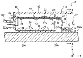
図1に示すように、センサ装置10は、被取付部材200へ取り付けられて、被取付部材200の温度を検出する装置である。本実施形態において、被取付部材200は、車両のウインドシールドである。被取付部材200は、一面200aと、一面200aと反対の裏面200bと、を有している。一面200aは、被取付部材200において、車両における室内側の面である。センサ装置10は、一面200aに配置されている。
As shown in FIG. 1, the
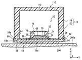
本実施形態において、センサ装置10は、レイン検出部20と、ライト検出部40と、温湿度検出部50と、ハウジング110と、コネクタ130と、を備えている。以下、被取付部材200に取り付けられた取付状態におけるセンサ装置10の概略構成について説明する。
In the present embodiment, the
レイン検出部20は、プリント基板22と、LED24と、レンズ26と、シート28と、PD30と、演算器32と、を有している。プリント基板22は、被取付部材200側の一面22aと、一面22aと反対の裏面22bと、を有している。一面22aには、LED24及びPD30が実装されている。裏面22bには、演算器32が実装されている。なお、演算器32が一面22aに実装された例を採用することもできる。LED24、PD30、及び演算器32は、特許請求の範囲に記載の電子部品に相当する。
The
LED24は、被取付部材200側に光を照射する。LED24の光は、レンズ26に入射する。レンズ26は、LED24の光を導光する部材である。レンズ26と被取付部材200との間には、シート28が配置されている。シート28は、柔軟性に優れた材料を用いて形成され、レンズ26及び被取付部材200に接触している。シート28としては、例えば、シリコーンシートを採用することができる。
The
LED24の光は、レンズ26及びシート28を介して被取付部材200に入射する。裏面200bに雨滴が付着している場合、LED24の光は、裏面200bで反射することなく、雨滴に入射する。一方、裏面200bに雨滴が付着していない場合、LED24の光は、裏面200bで反射する。裏面200bで反射したLED24の光は、シート28及びレンズ26を介してPD30に入射する。なお、レンズ26は、レイン検出部20及びライト検出部40と、温湿度検出部50と、を仕切るように一面22aに向かって延設された部分を有している。
The light of the
PD30は、LED24の光を受光し、受光強度に応じた検出信号を演算器32に出力する。演算器32は、PD30の検出信号に基づき、裏面200bに付着する雨滴の有無、又は、雨滴の量を判定する。演算器32は、例えば、制御回路、通信回路、演算回路を含んでいる。
The
ライト検出部40は、車両外部から入射する外光を検出するものである。ライト検出部40は、PD42、プリント基板22、演算器32を有している。PD42は、一面22aに実装されている。PD42には、被取付部材200、シート28及びレンズ26を介して、外光が入射する。PD42は、外光を受光し、受光強度に応じた検出信号を演算器32に出力する。演算器32は、PD42の検出信号に基づき、外光の有無、又は、外光の強度を判定する。PD42は、特許請求の範囲に記載の電子部品に相当する。なお、PD30及びPD42を、フォトダイオード、又は、受光素子と称することもできる。
The
温湿度検出部50は、温湿度検出素子52と、フレキシブル基板54と、剛性部材56と、柔軟性部材58と、を有している。温湿度検出素子52は、被取付部材200の温度、及び、被取付部材200の近傍の湿度を検出する素子である。詳しくは、温湿度検出素子52が、一面200aの温度、及び、一面200aの近傍の湿度を検出する。温湿度検出素子52は、特許請求の範囲に記載のセンサ素子に相当する。
The temperature and
温湿度検出素子52は、検出した温度及び湿度に応じた検出信号を、フレキシブル基板54及びプリント基板22を介して演算器32に出力する。演算器32は、温湿度検出素子52の検出信号に基づき、被取付部材200の温度、及び、一面200a近傍の湿度を算出する。演算器32が、温湿度検出素子52の検出信号に基づき、一面200aに付着する水滴の有無を判定する構成としてもよい。
The temperature and
フレキシブル基板54は、プリント基板22に接続された接続部60と、温湿度検出素子52が実装された実装部62と、実装部62及び接続部60の間に介在する介在部64を有している。接続部60は、プリント基板22と電気的に接続されている。接続部60は、例えば、コネクタ、はんだ、ACFを用いてプリント基板22と接続されている。なお、プリント基板22は、フレキシブル基板54よりも剛性に優れている。
The
図2に示すように、フレキシブル基板54は、一面54aと、一面54aと反対の裏面54bと、を有している。一面54aは、特許請求の範囲に記載の一面に相当する。裏面54bは、特許請求の範囲に記載の裏面に相当する。実装部62は、板厚方向がZ方向に沿う平板状をなしている。実装部62、剛性部材56、及び柔軟性部材58は、Z方向に積層されている。温湿度検出部50の構造については、下記で詳細に説明する。
As shown in FIG. 2, the
ハウジング110は、レイン検出部20及びライト検出部40を収容するとともに、温湿度検出部50を被取付部材200に押圧する部材である。ハウジング110は、レイン検出部20、ライト検出部40、及び温湿度検出部50を覆っている。ハウジング110は、少なくともプリント基板22を収容している。
The
ハウジング110は、図示しないばね要素とブラケットを介して被取付部材200に固定されている。ブラケットは、被取付部材200に接着されるとともに、ばね要素を介してハウジング110と嵌合している。なお、ハウジング110が、接着材のみを介して被取付部材200に固定された例を採用することもできる。
The
ハウジング110は、平板部112、側壁部114、及び押圧部116を有している。平板部112は、板厚方向がZ方向に沿う平板状をなしており、プリント基板22の裏面22b側に配置されている。平板部112は、Z方向の投影視において、レイン検出部20、ライト検出部40、及び温湿度検出部50と重なるように配置されている。
The
側壁部114は、平板部112において、Y方向の両端、及び、X方向の一端から、被取付部材200側に延設されている。さらに、側壁部114は、レイン検出部20及びライト検出部40と、温湿度検出部50と、を仕切るように、平板部112から裏面22bに向かって延設されている。なお、温湿度検出部50は、ハウジング110により密閉されていない。これにより、温湿度検出部50周囲の湿度を、センサ装置10の外部の空気における湿度とほぼ同じとすることができる。押圧部116の構造については、下記で詳細に説明する。
The
コネクタ130は、外部機器と演算器32とを電気的に中継するものである。コネクタ130は、ハウジング110と一体に成形、又は、ハウジング110に装着される。本実施形態では、コネクタ130がハウジング110に装着されている。
The
コネクタ130は、ターミナル132と、ターミナル132を保持する保持部134と、を有している。保持部134は、一面が開口する有底筒形状をなしている。保持部134の底部が、平板部112のX方向における一端から延設された側壁部114と嵌合している。保持部134、平板部112、及び側壁部114により、レイン検出部20及びライト検出部40を収容する空間が形成されている。
The
保持部134は、外部機器のコネクタと嵌合する。ターミナル132は、一端が保持部134の中空に位置して外部機器と接続され、他端がプリント基板22と接続されている。以上により、演算器32は、ターミナル132を介して外部機器との通信が可能とされている。
The holding
次に、図2及び図3に基づき、温湿度検出部50の詳細構造について説明する。
Next, the detailed structure of the temperature and
図2に示すように、温湿度検出素子52は、半導体基板66、温度検出部68、湿度検出部70、リードフレーム72、モールド樹脂74、透湿フィルタ76を有している。半導体基板66は、板厚方向がZ方向に沿う平板状をなしている。半導体基板66において、Z方向における被取付部材200と反対側の面には、温度検出部68及び湿度検出部70が形成されている。
As shown in FIG. 2, the temperature and
温度検出部68は、例えば、半導体基板66を表面処理することにより形成され、温度変化に応じて抵抗値が変化するものである。湿度検出部70は、例えば、感湿膜及び電極を有し、湿度変化に応じて感湿膜のインピーダンスが変化するものである。なお、半導体基板66は、リードフレーム72に配置されるとともに、リードフレーム72と電気的に接続されている。
The
リードフレーム72には、半導体基板66における被取付部材200側の面が固定されている。リードフレーム72は、ボンディングワイヤにより半導体基板66と電気的に接続されている。また、リードフレーム72は、フレキシブル基板54のランド82にはんだ接合されている。言い換えると、温湿度検出素子52は、フレキシブル基板54のランド82にはんだ接合されている。半導体基板66は、ボンディングワイヤ及びリードフレーム72を介してフレキシブル基板54と電気的に接続されている。すなわち、温湿度検出素子52は、はんだを介してランド82と電気的及び機械的に接続されている。
The surface of the
モールド樹脂74は、半導体基板66の一部、リードフレーム72の一部、及びボンディングワイヤを封止している。半導体基板66において、温度検出部68及び湿度検出部70は、モールド樹脂74から露出している。すなわち、半導体基板66は、モールド樹脂74により露出モールドされている。また、リードフレーム72におけるフレキシブル基板54との接続部分も、モールド樹脂74から露出している。
The
モールド樹脂74には、透湿フィルタ76が固定されている。透湿フィルタ76は、モールド樹脂74に貼着され、モールド樹脂74とともに内部空間78を形成する。この内部空間78には、温度検出部68及び湿度検出部70が露出している。
A moisture
フレキシブル基板54は、基材80及びランド82を有している。基材80は、電気絶縁性の材料を用いて形成されている。フレキシブル基板54は、基材80として、ベースフィルム及びカバーフィルムを有している。実装部62において、ベースフィルム及びカバーフィルムは、板厚方向がZ方向に沿う平板状をなしている。
The
ランド82は、フレキシブル基板54の電極であって、金属材料を用いて形成されている。ベースフィルムには、一部にランド82が配置され、ランド82が配置されない部分にカバーフィルムが配置されている。これにより、ランド82は、基材80から露出している。ランド82は、フレキシブル基板54において、少なくとも一面54a側に配置されている。本実施形態では、ランド82が一面54a側にのみ配置されている。
The
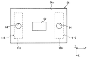
また、フレキシブル基板54は、図示しない配線層を有している。配線層は、ランド82と同様に、金属材料を用いて形成されている。配線層は、ベースフィルムにおいて、ランド82と異なる箇所に配置されるとともに、ランド82と電気的に接続されている。配線層は、カバーフィルムに被覆されている。言い換えると、配線層は、ベースフィルムとカバーフィルムとの間に配置されている。なお、実装部62には、下記の第1挿入部120が挿入配置される貫通孔84が形成されている。貫通孔84は、実装部62をZ方向に貫通している。
Also, the
剛性部材56は、基材80よりも熱伝導性及び剛性に優れた材料を用いて形成されている。剛性部材56は、例えば、樹脂材料、金属材料、セラミック材料を用いて形成される。本実施形態では、剛性部材56が、SUS、アルミニウム等の金属材料を用いて形成されている。剛性部材56は、板厚方向がZ方向に沿う平板状をなしている。
The
剛性部材56は、実装部62の裏面54bに接着されている。例えば、剛性部材56及びフレキシブル基板54は、接着材を介して互いに固定される。また、剛性部材56及びフレキシブル基板54が、熱圧着により互いに固定された例を採用することもできる。
The
実装部62には、下記の第1挿入部120が挿入配置される貫通孔86が形成されている。貫通孔86は、剛性部材56をZ方向に貫通している。剛性部材56における実装部62と反対側には、柔軟性部材58が配置されている。
The mounting
柔軟性部材58は、基材80よりも熱伝導性及び柔軟性に優れた材料を用いて形成されている。柔軟性部材58は、例えば、シリコーンシートにフィラーが添加されることにより形成される。柔軟性部材58は、板厚方向がZ方向に沿う平板状をなしている。
The
柔軟性部材58は、剛性部材56及び被取付部材200の間において、剛性部材56及び被取付部材200に接触して配置されている。詳しくは、柔軟性部材58が、剛性部材56及び被取付部材200に接着されている。なお、本実施形態では、剛性部材56における柔軟性部材58との接触面56aが、Z方向と直交する平面とされている。
The
温湿度検出素子52は、フレキシブル基板54のうちの、Z方向の投影視において剛性部材56及び柔軟性部材58と重なる部分である実装部62に配置されている。すなわち、温湿度検出素子52は、Z方向の投影視において、実装部62、剛性部材56、及び、柔軟性部材58と重なっている。
The temperature and
ハウジング110は、フレキシブル基板54を被取付部材200側に押圧する押圧部116を有している。ハウジング110は、特許請求の範囲に記載の押圧部材に相当する。押圧部116は、平板部112から被取付部材200側に延設された柱部118と、貫通孔84及び貫通孔86に挿入配置された第1挿入部120と、を有している。
The
柱部118は、延設方向がZ方向に沿う柱状をなしている。なお、図3では、柱部118を一点鎖線で示している。図3に示すように、柱部118の平面形状は、略矩形状をなしている。第1挿入部120は、柱部118における被取付部材200側の一端から突出している。第1挿入部120の平面形状は、貫通孔84の平面形状とほぼ同じ形状とされ、略円形状をなしている。
The
柱部118の平面形状は、第1挿入部120の平面形状よりも大きくされている。これにより、柱部118における被取付部材200側の一端において、第1挿入部120が形成されていない箇所が、一面54aと接触している。本実施形態において、柱部118及び第1挿入部120の個数は、それぞれ2つとされている。
The planar shape of the
組み付け工程において、貫通孔84及び貫通孔86に第1挿入部120を挿入して、フレキシブル基板54及び剛性部材56に対してハウジング110を配置する。第1挿入部120を貫通孔84及び貫通孔86を挿入することで、フレキシブル基板54及び剛性部材56に対してハウジング110を容易に位置決めすることができる。また、第1挿入部120が貫通孔84及び貫通孔86に挿入配置されることで、ハウジング110は、フレキシブル基板54及び剛性部材56に対して、Z方向と直交する方向に動くことが抑制される。
In the assembling process, the
次に、上記したセンサ装置10の効果について説明する。
Next, the effects of the above-described
本実施形態では、押圧部116の押圧により、柔軟性部材58が被取付部材200及び剛性部材56に密着する。剛性部材56は、フレキシブル基板54に接着されている。これらによれば、被取付部材200から柔軟性部材58、剛性部材56、及びフレキシブル基板54を介して温湿度検出素子52へ伝熱し易い。言い換えると、被取付部材200から温湿度検出素子52への熱伝導性を確保することができる。
In the present embodiment, the
また、本実施形態では、フレキシブル基板54が剛性部材56に接着されているため、組み付け工程においてフレキシブル基板54が変形し難い。したがって、フレキシブル基板54と温湿度検出素子52との電気的な接続信頼性が低下するのを抑制することができる。
Further, in the present embodiment, since the
また、本実施形態では、LED24、PD30、演算器32、PD42がプリント基板22に実装され、温湿度検出素子52がフレキシブル基板54に実装されている。これによれば、プリント基板22に実装された電子部品から温湿度検出素子52への伝熱を抑制することができる。
Further, in the present embodiment, the
(第2実施形態)
本実施形態において、第1実施形態に示したセンサ装置10と共通する部分についての説明は割愛する。
Second Embodiment
In the present embodiment, descriptions of parts common to the
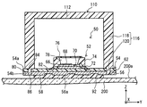
本実施形態では、第1実施形態と同様に、剛性部材56が金属材料を用いて形成されている。剛性部材56は、図示しない箇所で、フレキシブル基板54と電気的に接続されている。例えば、実装部62に対して、Z方向に沿って貫通孔を形成し、貫通孔が囲む空間にランド82を露出させる。この貫通孔にはんだを塗布することで、フレキシブル基板54と剛性部材56とを電気的に接続する。
In the present embodiment, as in the first embodiment, the
剛性部材56がフレキシブル基板54と電気的に接続されることで、剛性部材56の電位は所定電位に固定される。所定電位としては、例えば、電源電位、グランド電位を採用することができる。
By the
また、本実施形態では、図4に示すように、温湿度検出部50がコンデンサ88を有している。コンデンサ88は、剛性部材56の電位が変動するのを抑制するものである。コンデンサ88は、フレキシブル基板54及び剛性部材56と電気的に接続されている。本実施形態では、コンデンサ88が、チップコンデンサであって、一面54aに実装されている。
Further, in the present embodiment, as shown in FIG. 4, the temperature and
ところで、剛性部材56が金属材料を用いて形成された構成では、フレキシブル基板54と剛性部材56とが、寄生容量を介して電気的に接続され易い。フレキシブル基板54と剛性部材56とが寄生容量を介して剛性部材56と接続されると、フレキシブル基板54における剛性部材56との接続部分の電位が変動する虞がある。
By the way, in the configuration in which the
これに対し、本実施形態では、フレキシブル基板54と剛性部材56とが、寄生容量を介して電気的に接続されるのを抑制することができる。したがって、フレキシブル基板54における剛性部材56との接続部分の電位が変動するのを抑制することができる。また、本実施形態では、コンデンサ88により、フレキシブル基板54の電位が変動するのを効果的に抑制することができる。
On the other hand, in the present embodiment, the
(第3実施形態)
本実施形態において、第1実施形態に示したセンサ装置10と共通する部分についての説明は割愛する。
Third Embodiment
In the present embodiment, descriptions of parts common to the
図5に示すように、剛性部材56が、Z方向に沿って形成された貫通孔90を有している。Z方向の投影視において、貫通孔90は、柔軟性部材58と重なるように形成されている。XY平面において、貫通孔90は、貫通孔86と異なる箇所に形成されている。貫通孔90は、特許請求の範囲に記載の貫通孔に相当する。
As shown in FIG. 5, the
柔軟性部材58の一部は、貫通孔90に配置されている。詳しくは、組み付け工程において、押圧部116の押圧により、柔軟性部材58が、変形して貫通孔90に配置される。本実施形態では、複数の貫通孔90が形成されている。
A portion of the
本実施形態において、柔軟性部材58における貫通孔90に配置された部分は、剛性部材56に対して、Z方向と直交する方向に動くことが抑制される。これによれば、剛性部材56全体が柔軟性部材58に対して動くのを抑制することができる。
In the present embodiment, the portion of the
また、本実施形態では、剛性部材56に貫通孔90が形成されない構成に較べ、柔軟性部材58と剛性部材56との接触面積を大きくすることができる。したがって、柔軟性部材58から剛性部材56へ効果的に伝熱させることができる。
Further, in the present embodiment, the contact area between the
(第4実施形態)
本実施形態において、第1実施形態に示したセンサ装置10と共通する部分についての説明は割愛する。
Fourth Embodiment
In the present embodiment, descriptions of parts common to the
図6に示すように、剛性部材56の接触面56aが、凹凸形状をなしている。本実施形態では、剛性部材56に有底孔92が複数形成されることで、接触面56aが凹凸形状をなしている。有底孔92は、剛性部材56において、被取付部材200と反対側に凹んで形成されている。Z方向の投影視において、有底孔92は、柔軟性部材58と重なるように形成されている。XY平面において、有底孔92は、貫通孔86と異なる箇所に形成されている。
As shown in FIG. 6, the
柔軟性部材58の一部は、有底孔92に配置されている。詳しくは、組み付け工程において、押圧部116の押圧により、柔軟性部材58が、変形して有底孔92に配置される。
A portion of the
本実施形態では、接触面56aが平坦な面とされた構成に較べて、剛性部材56が柔軟性部材58に対して動くのを抑制することができる。また、接触面56aが平坦な構成に較べて、柔軟性部材58と剛性部材56との接触面積を大きくすることができ、柔軟性部材58から剛性部材56へ効果的に伝熱させることができる。
In the present embodiment, it is possible to suppress the movement of the
(第5実施形態)
本実施形態において、第1実施形態に示したセンサ装置10と共通する部分についての説明は割愛する。
Fifth Embodiment
In the present embodiment, descriptions of parts common to the
図7に示すように、温湿度検出部50が、温度検出素子94と湿度検出素子96とを有している。温度検出素子94は、被取付部材200の温度を検出する素子である。湿度検出素子96は、一面200aの近傍の湿度を検出する素子であって、温度検出素子94とは別に設けられている。
As shown in FIG. 7, the temperature and
フレキシブル基板54は、温度検出素子94と電気的に接続された第1ランド102と、湿度検出素子96と電気的に接続された第2ランド104と、を有している。第1ランド102及び第2ランド104は、一面54a側に配置されている。よって、温度検出素子94及び湿度検出素子96は、一面54aに実装されている。
The
(第6実施形態)
本実施形態において、第1実施形態に示したセンサ装置10と共通する部分についての説明は割愛する。
Sixth Embodiment
In the present embodiment, descriptions of parts common to the
図8に示すように、押圧部116は、フレキシブル基板54及び剛性部材56に対して、かしめ固定されている。押圧部116は、接触面56aに接触する第1接触部122を有している。第1接触部122は、第1挿入部120に対して被取付部材200側に配置されている。第1接触部122の平面形状は、貫通孔86の平面形状よりも大きくされている。フレキシブル基板54及び剛性部材56は、柱部118及び第1接触部122によりZ方向に挟持されている。第1接触部122は、例えば、熱かしめにより形成される。
As shown in FIG. 8, the
本実施形態では、フレキシブル基板54及び剛性部材56に対して、ハウジング110を強固に固定することができる。したがって、フレキシブル基板54及び剛性部材56に対してハウジング110が動くのを効果的に抑制することができる。
In the present embodiment, the
(第7実施形態)
本実施形態において、第1実施形態に示したセンサ装置10と共通する部分についての説明は割愛する。
Seventh Embodiment
In the present embodiment, descriptions of parts common to the
図9に示すように、ハウジング110は、第1挿入部120と異なる箇所でフレキシブル基板54に固定されている。フレキシブル基板54は、実装部62におけるY方向の両端からZ方向に延設された延設部98を有している。延設部98は、実装部62から被取付部材200と反対側へ延設されている。延設部98は、柱部118とY方向に対向している。延設部98は、Y方向に沿って形成された貫通孔100を有している。
As shown in FIG. 9, the
押圧部116は、貫通孔100に挿入配置された第2挿入部124と、延設部98における柱部118と反対側の面に接触する第2接触部126と、を有している。第2挿入部124は、柱部118からY方向における延設部98側へ突出している。第2接触部126は、第2挿入部124に対して柱部118と反対側に配置されている。
The
組み付け工程では、延設部98を変形させて貫通孔100に第2接触部126を通して、貫通孔100に第2挿入部124を挿入する。この方法では、第2接触部126をかしめにより形成する必要がない。したがって、本実施形態では、組み付け工程を簡素化しつつ、フレキシブル基板54及び剛性部材56に対して、ハウジング110を強固に固定することができる。
In the assembling process, the
(第8実施形態)
本実施形態において、第1実施形態に示したセンサ装置10と共通する部分についての説明は割愛する。
Eighth Embodiment
In the present embodiment, descriptions of parts common to the
以下、柔軟性部材58における剛性部材56側の面を一面58a、一面58aと反対の面を裏面58bと示す。一面58aは、柔軟性部材58における剛性部材56との接触面である。すなわち、一面58aは、接触面56aと接触している。裏面58bは、被取付部材200と接触する面である。
Hereinafter, the surface on the side of the
図10に示すように、本実施形態において柔軟性部材58は、シリコンシート58cとPETシート58dとを有している。なお、PETとは、ポリエチレンテフタレートのことである。以上によれば、柔軟性部材58は、シート状をなす2つの部材により構成されている。シリコンシート58cは、特許請求の範囲に記載の第1シートに相当する。PETシート58dは、特許請求の範囲に記載の第2シートに相当する。
As shown in FIG. 10, in the present embodiment, the
シリコンシート58cは、剛性部材56に接着されている。よって、シリコンシート58cにおける剛性部材56側の面が、柔軟性部材58の一面58aをなしている。シリコンシート58cの厚さは、例えば、1.5〜2.0mm程度とされている。シリコンシート58cにおける剛性部材56と反対側にPETシート58dが接着して配置されている。よって、Z方向において、被取付部材200、PETシート58d、シリコンシート58c、剛性部材56の順に並んでいる。
The
PETシート58dは、シリコンシート58c及び被取付部材200の間に配置され、シリコンシート58c及び被取付部材200の両方に接触している。すなわち、PETシート58dにおける被取付部材200側の面が、柔軟性部材58の裏面58bをなしている。PETシート58dの厚さは、シリコンシート58cの厚さに較べて薄くされ、例えば10〜20μm程度とされている。本実施形態では、PETシート58dの厚さが、12μm程度とされている。
The
シリコンシート58cは、PETシート58dに較べて接着性に優れている。言い換えると、PETシート58dは、シリコンシート58cに較べて接着性に劣っている。これによれば、一面58aは、裏面58bに較べて接着強度が高くされている。言い換えると、裏面58bは、一面58aに較べて接着強度が低くされている。さらに言い換えると、柔軟性部材では、剛性部材56側の一面58a、及び、被取付部材200側の裏面58bにおいて、接着強度に差が設けられている。
The
シリコンシート58cと剛性部材56との接着強度は、PETシート58dと被取付部材200との接着強度に較べて高くされている。言い換えると、PETシート58dと被取付部材200との接着強度は、シリコンシート58cと剛性部材56との接着強度に較べて低くされている。また、シリコンシート58cとPETシート58dとの接着強度は、PETシート58dと被取付部材200との接着強度に較べて高くされている。
The bonding strength between the
センサ装置10の組み付け方法としては、シリコンシート58cを剛性部材56に貼り付けるとともに、シリコンシート58cにPETシート58dを貼り付ける。そして、PETシート58dが一面200aと接触するように、センサ装置10を被取付部材200に配置する。
As a method of assembling the
ところで、被取付部材200が割れること等により、被取付部材200を取り替えることがある。この場合に、取り替える前の被取付部材200からセンサ装置10を取り外して、取り外したセンサ装置10を新たな被取付部材200に取り付けることが考えられる。すなわち、センサ装置10をリユースすることが考えられる。
By the way, the mounting
なお、ブラケットは被取付部材200に接着材を介して固定されている。そのため、ブラケットは被取付部材200から取り外し難い。したがって、センサ装置10をリユースする際には、取り替える前の被取付部材200からブラケットを取り外すことなく、新たなブラケットを用いる。
The bracket is fixed to the mounting
センサ装置10を被取付部材200から取り外す方法としては、ばね要素をブラケットから取り外す。これにより、センサ装置10におけるブラケット以外の部分を被取付部材200から取り外すことができる。このとき、柔軟性部材58と被取付部材200との接着強度が高いと、柔軟性部材58を被取付部材200から取り外し難い。この場合には、ブラケットと同様に、センサ装置10をリユースする際に新たな柔軟性部材58を用いる必要がある。
As a method of removing the
これに対し本実施形態では、裏面58bの接着強度が、一面58aの接着強度に較べて低くされている。そのため、PETシート58dと被取付部材200との接着強度は、シリコンシート58cと剛性部材56との接着強度に較べて低くされる。これによれば、センサ装置10を被取付部材200から取り外す際に、柔軟性部材58を被取付部材200から取り外し易い。したがって、センサ装置10をリユースする際に、取り替える前の被取付部材200に接触していた柔軟性部材58を取り外して新たな被取付部材200に取り付けることができる。よって、新たな柔軟性部材58を用いるコストを抑制することができる。
On the other hand, in the present embodiment, the adhesive strength of the
また本実施形態では、一面58aの接着強度が、裏面58bの接着強度に較べて高くされている。そのため、シリコンシート58cと剛性部材56との接着強度は、PETシート58dと被取付部材200との接着強度に較べて高くされる。さらに本実施形態では、シリコンシート58cとPETシート58dとの接着強度が、PETシート58dと被取付部材200との接着強度に較べて高くされる。
Further, in the present embodiment, the adhesive strength of the one
これによれば、センサ装置10を被取付部材200から取り外す際に、シリコンシート58cが剛性部材56から離れ難く、且つ、シリコンシート58cからPETシート58dが離れ難い。すなわち、剛性部材56から柔軟性部材58が離れ難い。したがって、センサ装置10を新たな被取付部材200に取り付ける際に、剛性部材56に柔軟性部材58を貼り直す必要がない。すなわち、センサ装置10をリユースする際に、センサ装置10を被取付部材200に取り付ける工程を簡略化することができる。
According to this, when the
なお、本実施形態において柔軟性部材58はシリコンシート58cとPETシート58dとを有する例を示したが、これに限定するものではない。図11の第1変形例に示すように、柔軟性部材58が、接着性に優れた第1層58eと、第1層58eよりも接着性に劣る第2層58fと、を有するシリコンシートとされた例を採用することもできる。なお図11では、便宜上、第1層58eと第2層58fとの境界を破線で示している。
In the present embodiment, the
第1層58eは、剛性部材56に接着されている。すなわち、第1層58eにおける剛性部材56側の面が、柔軟性部材58の一面58aをなしている。第1層58eにおける剛性部材56と反対側に第2層58fが形成されている。第2層58fは、被取付部材200に接触している。すなわち、第2層58fにおける被取付部材200側の面が、柔軟性部材58の裏面58bをなしている。
The
第1層58eは、一面58a側からシリコンシートに紫外線(UV)が照射されることによって形成されている。すなわち、シリコンシートにUV処理が施されることによって第1層58eが形成されている。
The
UV処理が施された部分である第1層58eは、UV処理の影響を受けていない部分である第2層58fに較べて、接着性に優れている。これにより、一面58aは、裏面58bに較べて接着強度が高くされている。第1層58eと剛性部材56との接着強度は、第2層58fと被取付部材200との接着強度に較べて高くされている。言い換えると、第2層58fと被取付部材200との接着強度は、第1層58eと剛性部材56との接着強度に較べて低くされている。
The
また、図12の第2変形例に示すように、剛性部材56に対して液状の樹脂をポッティングすることにより、柔軟性部材58を形成してもよい。剛性部材56に対して樹脂をポッティングした後、加熱等により、樹脂を硬化させる。これにより柔軟性部材58を形成することができる。硬化により柔軟性部材58を形成した後、柔軟性部材58の裏面58bが一面200aと接触するように、センサ装置10を被取付部材200に配置する。
Further, as shown in the second modified example of FIG. 12, the
この例では、ポッティングの際、樹脂が、液状であるため、接触面56aに形成された微細な凹凸に入り込む。したがって、シリコンシートを剛性部材56に配置する方法に較べて、柔軟性部材58と剛性部材56との接触面積を大きくすることができる。また、ポッティングする樹脂の結合手は、硬化することによって数が少なくなる。そのため、ポッティングの際に剛性部材56と接触する樹脂の結合手は多く、センサ装置10を被取付部材200に配置する際に被取付部材200と接触する柔軟性部材58の結合手は少ない。以上によれば、裏面58bは、一面58aに較べて接着強度が低くされる。
In this example, at the time of potting, since the resin is in a liquid state, the resin enters the fine unevenness formed on the
図13の第3変形例に示すように、柔軟性部材58が、プライマー58gとシリコンシート58hとを有する例を採用することもできる。プライマー58gとは、粘着剤である。なお、プライマー58gが接着材であってもよい。
As shown in the third modified example of FIG. 13, an example in which the
プライマー58gは、シリコンシート58hに塗布され、シリコンシート58hを剛性部材56に接着している。すなわち、プライマー58gは、剛性部材56及びシリコンシート58hの両方に接着されている。プライマー58gにおける剛性部材56側の面が、柔軟性部材58の一面58aに相当する。
The
シリコンシート58hにおけるプライマー58gと反対側の面が、被取付部材200に接触している。すなわち、シリコンシート58hにおける被取付部材200側の面が、柔軟性部材58の裏面58bをなしている。
The surface of the
プライマー58gと剛性部材56との接着強度は、シリコンシート58hと被取付部材200との接着強度に較べて高くされている。言い換えると、シリコンシート58hと被取付部材200との接着強度は、プライマー58gと剛性部材56との接着強度に較べて低くされている。また、プライマー58gとシリコンシート58hとの接着強度は、シリコンシート58hと被取付部材200との接着強度に較べて高くされている。
The bonding strength between the
なお、第3変形例において、第8実施形態と同様に、シリコンシート58hと被取付部材200との間にPETシートが配置されていてもよい。すなわち、柔軟性部材58が、プライマ−58g及びシリコンシート58hに加えて、PETシートを有していてもよい。また、第3変形例において、第1変形例と同様に、シリコンシート58hは、裏面58b側からUV処理が施されていてもよい。
In the third modification, as in the eighth embodiment, a PET sheet may be disposed between the
以上、本発明の好ましい実施形態について説明したが、本発明は上記実施形態になんら制限されることなく、本発明の主旨を逸脱しない範囲において、種々変形して実施することが可能である。 The preferred embodiments of the present invention have been described above. However, the present invention is not limited to the above-described embodiments and can be variously modified and implemented without departing from the spirit of the present invention.
また、上記実施形態では、温湿度検出素子52が、フレキシブル基板54にはんだ接合された例を示したが、これに限定するものではない。温湿度検出素子52が、ボンディングワイヤ、銀ペーストにより、フレキシブル基板54と電気的に接続された例を採用することもできる。
Moreover, although the temperature and
また、上記実施形態では、センサ装置10が、レイン検出部20、ライト検出部40、温湿度検出部50、ハウジング110、コネクタ130を備える例を示した。しかしながら、これに限定するものではない。センサ装置10は、被取付部材200に取り付けられ、被取付部材200の温度を検出する構成であれば採用することができる。
Moreover, in the said embodiment, the
また、上記実施形態では、温湿度検出素子52が、半導体基板66、リードフレーム72、モールド樹脂74、透湿フィルタ76を有する例を示した。しかしながら、これに限定するものではない。温湿度検出素子52が、リードフレーム72、モールド樹脂74を有さない例を採用することもできる。また、半導体基板66がセラミックケース又は樹脂ケースに収容された例を採用することもできる。
Moreover, in the said embodiment, the temperature /
また、上記実施形態では、押圧部116が、柱部118及び第1挿入部120を有する例を示したが、これに限定するものではない。柱部118及び第1挿入部120の個数が、それぞれ2つである例を示したが、これに限定するものではない。柱部118の平面形状が略矩形状とされ、第1挿入部120の平面形状が略円形状とされた例を示したが、これに限定するものではない。
Moreover, in the said embodiment, although the
10…センサ装置、20…レイン検出部、22…プリント基板、40…ライト検出部、50…温湿度検出部、52…温湿度検出素子、54…フレキシブル基板、54a…一面、54b…裏面、56…剛性部材、56a…接触面、58…柔軟性部材、62…実装部、66…半導体基板、68…温度検出部、70…湿度検出部、72…リードフレーム、74…モールド樹脂、76…透湿フィルタ、80…基材、82…ランド、84…貫通孔、86…貫通孔、88…コンデンサ、90…貫通孔、92…有底孔、94…温度検出素子、96…湿度検出素子、98…延設部、100…貫通孔、102…第1ランド、104…第2ランド、110…ハウジング、112…平板部、116…押圧部、130…コネクタ、200…被取付部材
DESCRIPTION OF
Claims (17)
一面(54a)及び該一面と反対の裏面(54b)を有するとともに、電気絶縁性の材料を用いて形成された基材(80)と、前記一面側に配置され、前記センサ素子と電気的に接続されたランド(82,102)と、を有するフレキシブル基板(54)と、
前記基材よりも熱伝導性及び剛性に優れるとともに、前記裏面に接着された剛性部材(56)と、
前記基材よりも熱伝導性及び柔軟性に優れるとともに、前記剛性部材における前記フレキシブル基板の反対側に接触して前記剛性部材に積層され、前記取付状態で前記被取付部材に接触して配置される柔軟性部材(58)と、
前記取付状態で、前記フレキシブル基板を前記被取付部材側に押圧する押圧部材(110)と、を備え、
前記剛性部材は、金属材料を用いて形成されるとともに、前記フレキシブル基板と電気的に接続されて、所定電位に固定されることを特徴とするセンサ装置。 A sensor device comprising a sensor element (52, 94) for detecting a temperature and detecting the temperature of the attached member by the sensor element in an attached state attached to the attached member (200),
A substrate (80) having one surface (54a) and a back surface (54b) opposite to the one surface, and being formed using an electrically insulating material, and disposed on the one surface side electrically with the sensor element A flexible substrate (54) having lands (82, 102) connected to each other;
A rigid member (56) which is superior in thermal conductivity and rigidity to the base material and is bonded to the back surface;
It is superior in thermal conductivity and flexibility than the base material, is in contact with the opposite side of the flexible substrate in the rigid member, is laminated on the rigid member, and is disposed in contact with the attached member in the attached state Flexible member (58),
And a pressing member (110) for pressing the flexible substrate toward the mounting member in the mounting state.
The sensor device, wherein the rigid member is formed using a metal material, is electrically connected to the flexible substrate, and is fixed at a predetermined potential.
一面(54a)及び該一面と反対の裏面(54b)を有するとともに、電気絶縁性の材料を用いて形成された基材(80)と、前記一面側に配置され、前記センサ素子と電気的に接続されたランド(82,102)と、を有するフレキシブル基板(54)と、
前記基材よりも熱伝導性及び剛性に優れるとともに、前記裏面に接着された剛性部材(56)と、
前記基材よりも熱伝導性及び柔軟性に優れるとともに、前記剛性部材における前記フレキシブル基板の反対側に接触して前記剛性部材に積層され、前記取付状態で前記被取付部材に接触して配置される柔軟性部材(58)と、
前記取付状態で、前記フレキシブル基板を前記被取付部材側に押圧する押圧部材(110)と、を備え、
前記剛性部材は、前記剛性部材及び前記柔軟性部材の積層方向に沿って形成されるとともに、前記積層方向の投影視において前記柔軟性部材と重なるように形成された貫通孔(90)を有し、
前記取付状態で、前記柔軟性部材の一部は、前記貫通孔に配置されていることを特徴とするセンサ装置。 A sensor device comprising a sensor element (52, 94) for detecting a temperature and detecting the temperature of the attached member by the sensor element in an attached state attached to the attached member (200),
A substrate (80) having one surface (54a) and a back surface (54b) opposite to the one surface, and being formed using an electrically insulating material, and disposed on the one surface side electrically with the sensor element A flexible substrate (54) having lands (82, 102) connected to each other;
A rigid member (56) which is superior in thermal conductivity and rigidity to the base material and is bonded to the back surface;
It is superior in thermal conductivity and flexibility than the base material, is in contact with the opposite side of the flexible substrate in the rigid member, is laminated on the rigid member, and is disposed in contact with the attached member in the attached state Flexible member (58),
And a pressing member (110) for pressing the flexible substrate toward the mounting member in the mounting state.
The rigid member is formed along the stacking direction of the rigid member and the flexible member, and has a through hole (90) formed so as to overlap the flexible member in projection view of the stacking direction ,
In the attached state, a part of the flexible member is disposed in the through hole.
一面(54a)及び該一面と反対の裏面(54b)を有するとともに、電気絶縁性の材料を用いて形成された基材(80)と、前記一面側に配置され、前記センサ素子と電気的に接続されたランド(82,102)と、を有するフレキシブル基板(54)と、
前記基材よりも熱伝導性及び剛性に優れるとともに、前記裏面に接着された剛性部材(56)と、
前記基材よりも熱伝導性及び柔軟性に優れるとともに、前記剛性部材における前記フレキシブル基板の反対側に接触して前記剛性部材に積層され、前記取付状態で前記被取付部材に接触して配置される柔軟性部材(58)と、
前記取付状態で、前記フレキシブル基板を前記被取付部材側に押圧する押圧部材(110)と、を備え、
前記剛性部材は、前記柔軟性部材との接触面(56a)が、凹凸形状をなしていることを特徴とするセンサ装置。 A sensor device comprising a sensor element (52, 94) for detecting a temperature and detecting the temperature of the attached member by the sensor element in an attached state attached to the attached member (200),
A substrate (80) having one surface (54a) and a back surface (54b) opposite to the one surface, and being formed using an electrically insulating material, and disposed on the one surface side electrically with the sensor element A flexible substrate (54) having lands (82, 102) connected to each other;
A rigid member (56) which is superior in thermal conductivity and rigidity to the base material and is bonded to the back surface;
It is superior in thermal conductivity and flexibility than the base material, is in contact with the opposite side of the flexible substrate in the rigid member, is laminated on the rigid member, and is disposed in contact with the attached member in the attached state Flexible member (58),
And a pressing member (110) for pressing the flexible substrate toward the mounting member in the mounting state.
A sensor device characterized in that the contact surface (56a) of the rigid member with the flexible member has an uneven shape.
一面(54a)及び該一面と反対の裏面(54b)を有するとともに、電気絶縁性の材料を用いて形成された基材(80)と、前記一面側に配置され、前記センサ素子と電気的に接続されたランド(82,102)と、を有するフレキシブル基板(54)と、
前記基材よりも熱伝導性及び剛性に優れるとともに、前記裏面に接着された剛性部材(56)と、
前記基材よりも熱伝導性及び柔軟性に優れるとともに、前記剛性部材における前記フレキシブル基板の反対側に接触して前記剛性部材に積層され、前記取付状態で前記被取付部材に接触して配置される柔軟性部材(58)と、
前記取付状態で、前記フレキシブル基板を前記被取付部材側に押圧する押圧部材(110)と、を備え、
前記柔軟性部材では、前記取付状態で前記被取付部材と接触する面(58a)の接着強度が、前記剛性部材と接触している面(58b)の接着強度よりも低くされていることを特徴とするセンサ装置。 A sensor device comprising a sensor element (52, 94) for detecting a temperature and detecting the temperature of the attached member by the sensor element in an attached state attached to the attached member (200),
A substrate (80) having one surface (54a) and a back surface (54b) opposite to the one surface, and being formed using an electrically insulating material, and disposed on the one surface side electrically with the sensor element A flexible substrate (54) having lands (82, 102) connected to each other;
A rigid member (56) which is superior in thermal conductivity and rigidity to the base material and is bonded to the back surface;
It is superior in thermal conductivity and flexibility than the base material, is in contact with the opposite side of the flexible substrate in the rigid member, is laminated on the rigid member, and is disposed in contact with the attached member in the attached state Flexible member (58),
And a pressing member (110) for pressing the flexible substrate toward the mounting member in the mounting state.
In the flexible member, the adhesive strength of the surface (58a) in contact with the mounting member in the mounted state is lower than the adhesive strength of the surface (58b) in contact with the rigid member. Sensor device to be.
一面(54a)及び該一面と反対の裏面(54b)を有するとともに、電気絶縁性の材料を用いて形成された基材(80)と、前記一面側に配置され、前記センサ素子と電気的に接続されたランド(82,102)と、を有するフレキシブル基板(54)と、
前記基材よりも熱伝導性及び剛性に優れるとともに、前記裏面に接着された剛性部材(56)と、
前記基材よりも熱伝導性及び柔軟性に優れるとともに、前記剛性部材における前記フレキシブル基板の反対側に接触して前記剛性部材に積層され、前記取付状態で前記被取付部材に接触して配置される柔軟性部材(58)と、
前記取付状態で、前記フレキシブル基板を前記被取付部材側に押圧する押圧部材(110)と、を備え、
前記フレキシブル基板よりも剛性に優れ、前記フレキシブル基板と電気的に接続されたプリント基板(22)と、
前記プリント基板に実装された電子部品(24,30,32,42)と、
をさらに備えていることを特徴とするセンサ装置。 A sensor device comprising a sensor element (52, 94) for detecting a temperature and detecting the temperature of the attached member by the sensor element in an attached state attached to the attached member (200),
A substrate (80) having one surface (54a) and a back surface (54b) opposite to the one surface, and being formed using an electrically insulating material, and disposed on the one surface side electrically with the sensor element A flexible substrate (54) having lands (82, 102) connected to each other;
A rigid member (56) which is superior in thermal conductivity and rigidity to the base material and is bonded to the back surface;
It is superior in thermal conductivity and flexibility than the base material, is in contact with the opposite side of the flexible substrate in the rigid member, is laminated on the rigid member, and is disposed in contact with the attached member in the attached state Flexible member (58),
And a pressing member (110) for pressing the flexible substrate toward the mounting member in the mounting state.
A printed circuit board (22) which is more rigid than the flexible substrate and electrically connected to the flexible substrate;
Electronic components (24, 30, 32, 42) mounted on the printed circuit board;
A sensor device characterized by further comprising:
前記取付状態で、前記柔軟性部材の一部は、前記貫通孔に配置されていることを特徴とする請求項1、3〜7のいずれか1項に記載のセンサ装置。 The rigid member is formed along the stacking direction of the rigid member and the flexible member, and has a through hole (90) formed so as to overlap the flexible member in projection view of the stacking direction ,
The sensor device according to any one of claims 1 to 7, wherein a part of the flexible member is disposed in the through hole in the attached state.
前記第1シートは、前記第2シートよりも接着性に優れている請求項4または請求項10に記載のセンサ装置。 The flexible member is disposed on the first sheet (58c) adhered to the rigid member and adhered to the side opposite to the flexible member with respect to the first sheet. And a second sheet (58d) in contact with the member;
The sensor device according to claim 4, wherein the first sheet is more adhesive than the second sheet.
前記プリント基板に実装された電子部品(24,30,32,42)と、
をさらに備えていることを特徴とする請求項1〜4のいずれか1項に記載のセンサ装置。 A printed circuit board (22) which is more rigid than the flexible substrate and electrically connected to the flexible substrate;
Electronic components (24, 30, 32, 42) mounted on the printed circuit board;
The sensor device according to any one of claims 1 to 4 , further comprising:
前記フレキシブル基板は、前記一面側に配置された第2ランド(104)を有し、
前記第2ランドと電気的に接続され、前記取付状態で、前記被取付部材の近傍の湿度を検出する湿度検出素子(96)をさらに備えることを特徴とする請求項1〜13のいずれか1項に記載のセンサ装置。 The land is a first land,
The flexible substrate has a second land (104) disposed on the one surface side,
The humidity detection element (96) according to any one of claims 1 to 13, further comprising a humidity detection element (96) electrically connected to the second land and detecting the humidity in the vicinity of the mounting member in the mounted state. Sensor device given in paragraph.
Priority Applications (3)
| Application Number | Priority Date | Filing Date | Title |
|---|---|---|---|
| PCT/JP2016/002511 WO2016194334A1 (en) | 2015-06-01 | 2016-05-24 | Sensor device |
| US15/559,109 US10527498B2 (en) | 2015-06-01 | 2016-05-24 | Sensor device |
| DE112016002445.2T DE112016002445B4 (en) | 2015-06-01 | 2016-05-24 | Sensor device |
Applications Claiming Priority (2)
| Application Number | Priority Date | Filing Date | Title |
|---|---|---|---|
| JP2015111728 | 2015-06-01 | ||
| JP2015111728 | 2015-06-01 |
Publications (3)
| Publication Number | Publication Date |
|---|---|
| JP2016224037A JP2016224037A (en) | 2016-12-28 |
| JP2016224037A5 JP2016224037A5 (en) | 2017-07-06 |
| JP6536474B2 true JP6536474B2 (en) | 2019-07-03 |
Family
ID=57748651
Family Applications (1)
| Application Number | Title | Priority Date | Filing Date |
|---|---|---|---|
| JP2016093519A Expired - Fee Related JP6536474B2 (en) | 2015-06-01 | 2016-05-07 | Sensor device |
Country Status (3)
| Country | Link |
|---|---|
| US (1) | US10527498B2 (en) |
| JP (1) | JP6536474B2 (en) |
| DE (1) | DE112016002445B4 (en) |
Families Citing this family (5)
| Publication number | Priority date | Publication date | Assignee | Title |
|---|---|---|---|---|
| US10433387B2 (en) * | 2016-12-28 | 2019-10-01 | Asahi Kasei Microdevices Corporation | Light emitting device and light emitting and receiving device |
| JP2019074327A (en) | 2017-10-12 | 2019-05-16 | 株式会社オートネットワーク技術研究所 | Sensor unit and power storage module |
| EP3628540B1 (en) * | 2018-09-25 | 2022-03-16 | MEAS France | Windshield sensing device |
| JP7068397B2 (en) * | 2020-08-06 | 2022-05-16 | 株式会社オートネットワーク技術研究所 | Sensor unit and power storage module |
| JP7293453B2 (en) | 2020-08-06 | 2023-06-19 | 株式会社オートネットワーク技術研究所 | Sensor unit and power storage module |
Family Cites Families (17)
| Publication number | Priority date | Publication date | Assignee | Title |
|---|---|---|---|---|
| JPS6255157U (en) | 1985-09-27 | 1987-04-06 | ||
| US5370459A (en) * | 1993-06-08 | 1994-12-06 | Claud S. Gordon Company | Surface temperature probe with uniform thermocouple junction |
| JP3223716B2 (en) * | 1994-08-30 | 2001-10-29 | 三菱マテリアル株式会社 | Thermistor sensor |
| JP4712929B2 (en) * | 1999-09-21 | 2011-06-29 | パナソニック株式会社 | Abnormal temperature detection device for battery pack |
| JP2003337112A (en) | 2002-05-21 | 2003-11-28 | Asahi Glass Co Ltd | Window glass with dew formation sensor |
| JP2006258520A (en) * | 2005-03-16 | 2006-09-28 | Ishizuka Electronics Corp | Probe for electronic clinical thermometer |
| DE102005016896B3 (en) * | 2005-04-12 | 2006-10-26 | Sitronic Gesellschaft für elektrotechnische Ausrüstung mbH. & Co. KG | Sensor arrangement for temperature measurement |
| EP1700724B1 (en) | 2006-07-19 | 2009-09-02 | Sensirion Holding AG | Humidity detector for detecting fogging on a window |
| DE102006060548B4 (en) | 2006-12-21 | 2022-12-08 | HELLA GmbH & Co. KGaA | Optoelectronic rain sensor unit for motor vehicles |
| DE102006060546B4 (en) | 2006-12-21 | 2020-10-08 | HELLA GmbH & Co. KGaA | Optoelectronic rain sensor unit for motor vehicles |
| US8496377B2 (en) * | 2007-12-31 | 2013-07-30 | Covidien Lp | Thermometer having molded probe component |
| JP5248360B2 (en) * | 2009-02-10 | 2013-07-31 | 矢崎総業株式会社 | Circuit structure for temperature detection |
| DE102011122456A1 (en) | 2011-12-24 | 2013-06-27 | Valeo Schalter Und Sensoren Gmbh | Optical sensor with an integrated humidity sensor |
| JP2014038056A (en) * | 2012-08-20 | 2014-02-27 | Hitachi Automotive Systems Ltd | Humidity detector |
| JP3184781U (en) | 2013-04-15 | 2013-07-18 | 祥 田邉 | Surface temperature sensor |
| JP6083351B2 (en) * | 2013-08-06 | 2017-02-22 | 株式会社デンソー | Integrated sensor device, manufacturing method thereof, and contact member |
| US10113915B1 (en) * | 2015-05-19 | 2018-10-30 | Maxim Integrated Products, Inc. | Non-contact temperature measurement sensor |
-
2016
- 2016-05-07 JP JP2016093519A patent/JP6536474B2/en not_active Expired - Fee Related
- 2016-05-24 DE DE112016002445.2T patent/DE112016002445B4/en not_active Expired - Fee Related
- 2016-05-24 US US15/559,109 patent/US10527498B2/en not_active Expired - Fee Related
Also Published As
| Publication number | Publication date |
|---|---|
| DE112016002445B4 (en) | 2023-10-05 |
| DE112016002445T5 (en) | 2018-02-22 |
| US20180156670A1 (en) | 2018-06-07 |
| JP2016224037A (en) | 2016-12-28 |
| US10527498B2 (en) | 2020-01-07 |
Similar Documents
| Publication | Publication Date | Title |
|---|---|---|
| JP6536474B2 (en) | Sensor device | |
| JP5277755B2 (en) | Electronic components | |
| JP4763724B2 (en) | Control module | |
| KR101364486B1 (en) | Test carrier | |
| JP6666927B2 (en) | Electronic control unit | |
| JP3546059B2 (en) | Pressure sensor components that can be assembled on the mounting surface of a printed wiring board | |
| JP5889718B2 (en) | Electronic component mounting structure and input device, and method of manufacturing the mounting structure | |
| US6649834B1 (en) | Injection molded image sensor and a method for manufacturing the same | |
| TW200701430A (en) | Semiconductor device and manufacturing method therefor | |
| JP2018506855A (en) | Electronic component and method for manufacturing such an electronic component | |
| US10964623B2 (en) | Electronic module and method for encapsulation thereof | |
| JP2006084232A (en) | Capacitance type humidity sensor | |
| WO2022188524A1 (en) | Packaging module, packaging process, and electronic device | |
| JP5458517B2 (en) | Electronic components | |
| CN111422819A (en) | Sensor packaging structure, packaging method thereof and electronic equipment | |
| TW201408149A (en) | Circuit board assembly and camera module | |
| JP7455585B2 (en) | How to interconnect sensor units and substrates and carriers | |
| JP6666048B2 (en) | Circuit board device | |
| WO2016194334A1 (en) | Sensor device | |
| EP3456682B1 (en) | Sensor system, sensor arrangement, and assembly method using solder for sealing | |
| WO2019102737A1 (en) | Flow rate meter | |
| JP2005228782A (en) | Electronic component mounting structure onto flexible board | |
| JP5555974B2 (en) | Piezoelectric device, electronic device using the same, and automobile | |
| US20200152482A1 (en) | Semiconductor device and method for producing the semiconductor device | |
| CN209927304U (en) | Surface-mounted pyroelectric sensor |
Legal Events
| Date | Code | Title | Description |
|---|---|---|---|
| A521 | Request for written amendment filed |
Free format text: JAPANESE INTERMEDIATE CODE: A523 Effective date: 20170526 |
|
| A621 | Written request for application examination |
Free format text: JAPANESE INTERMEDIATE CODE: A621 Effective date: 20170526 |
|
| A131 | Notification of reasons for refusal |
Free format text: JAPANESE INTERMEDIATE CODE: A131 Effective date: 20180529 |
|
| A521 | Request for written amendment filed |
Free format text: JAPANESE INTERMEDIATE CODE: A523 Effective date: 20180723 |
|
| A131 | Notification of reasons for refusal |
Free format text: JAPANESE INTERMEDIATE CODE: A131 Effective date: 20181211 |
|
| A521 | Request for written amendment filed |
Free format text: JAPANESE INTERMEDIATE CODE: A523 Effective date: 20190204 |
|
| TRDD | Decision of grant or rejection written | ||
| A01 | Written decision to grant a patent or to grant a registration (utility model) |
Free format text: JAPANESE INTERMEDIATE CODE: A01 Effective date: 20190507 |
|
| A61 | First payment of annual fees (during grant procedure) |
Free format text: JAPANESE INTERMEDIATE CODE: A61 Effective date: 20190520 |
|
| R151 | Written notification of patent or utility model registration |
Ref document number: 6536474 Country of ref document: JP Free format text: JAPANESE INTERMEDIATE CODE: R151 |
|
| LAPS | Cancellation because of no payment of annual fees |