JP6533501B2 - Light irradiation device - Google Patents

Light irradiation device Download PDF

Info

Publication number
JP6533501B2
JP6533501B2 JP2016165194A JP2016165194A JP6533501B2 JP 6533501 B2 JP6533501 B2 JP 6533501B2 JP 2016165194 A JP2016165194 A JP 2016165194A JP 2016165194 A JP2016165194 A JP 2016165194A JP 6533501 B2 JP6533501 B2 JP 6533501B2
Authority
JP
Japan
Prior art keywords
substrate
axis direction
light
light irradiation
led elements
Prior art date
Legal status (The legal status is an assumption and is not a legal conclusion. Google has not performed a legal analysis and makes no representation as to the accuracy of the status listed.)
Active
Application number
JP2016165194A
Other languages
Japanese (ja)
Other versions
JP2018032799A (en
Inventor
正志 藤野
正志 藤野
Current Assignee (The listed assignees may be inaccurate. Google has not performed a legal analysis and makes no representation or warranty as to the accuracy of the list.)
Hoya Candeo Optronics Corp
Original Assignee
Hoya Candeo Optronics Corp
Priority date (The priority date is an assumption and is not a legal conclusion. Google has not performed a legal analysis and makes no representation as to the accuracy of the date listed.)
Filing date
Publication date
Application filed by Hoya Candeo Optronics Corp filed Critical Hoya Candeo Optronics Corp
Priority to JP2016165194A priority Critical patent/JP6533501B2/en
Publication of JP2018032799A publication Critical patent/JP2018032799A/en
Application granted granted Critical
Publication of JP6533501B2 publication Critical patent/JP6533501B2/en
Active legal-status Critical Current
Anticipated expiration legal-status Critical

Links

Images

Description

本発明は、一方向に相対的に移動する照射対象物に対して、ライン状の光を照射する光照射装置に関し、特に、複数の光源がライン状に配置された光照射モジュールを複数備えた光照射装置に関する。   The present invention relates to a light irradiation apparatus for irradiating line-shaped light to an irradiation object relatively moving in one direction, and in particular, includes a plurality of light irradiation modules in which a plurality of light sources are arranged in a line. The present invention relates to a light irradiation device.

従来、オフセット枚葉印刷用のインキとして、紫外光の照射により硬化する紫外線硬化型インキが用いられている。また、液晶パネルや有機EL(Electro Luminescence)パネル等、FPD(Flat Panel Display)回りの接着剤として、紫外線硬化樹脂が用いられている。このような紫外線硬化型インキや紫外線硬化樹脂の硬化には、一般に、紫外光を照射する紫外光照射装置が用いられるが、特にオフセット枚葉印刷やFPDの用途においては、幅広の照射領域を照射する必要があるため、ライン状の照射光を照射する紫外光照射装置が用いられる。   Conventionally, as an ink for offset sheet-fed printing, an ultraviolet curable ink which is cured by irradiation of ultraviolet light is used. In addition, an ultraviolet curing resin is used as an adhesive agent around a flat panel display (FPD) such as a liquid crystal panel or an organic EL (electro luminescence) panel. An ultraviolet light irradiation device for irradiating ultraviolet light is generally used to cure such ultraviolet curable ink and ultraviolet curable resin, but in particular in applications of offset sheet-fed printing and FPD, a wide irradiation region is irradiated Since it is necessary to use an ultraviolet light irradiation apparatus for irradiating line-shaped irradiation light.

紫外光照射装置としては、従来から高圧水銀ランプや水銀キセノンランプ等を光源とするランプ型照射装置が知られているが、近年、消費電力の削減、長寿命化、装置サイズのコンパクト化の要請から、従来の放電ランプに替えて、LEDを光源として利用した紫外光照射装置が開発されている。   As an ultraviolet light irradiation apparatus, a lamp type irradiation apparatus using a high pressure mercury lamp, a mercury xenon lamp, etc. as a light source has been known conventionally, but in recent years, a demand for reduction of power consumption, prolongation of life, and downsizing of apparatus size Therefore, instead of the conventional discharge lamp, an ultraviolet light irradiation apparatus using an LED as a light source has been developed.

このようなLEDを光源として利用した紫外光照射装置は、例えば、特許文献1に記載されている。特許文献1に記載の紫外光照射装置は、複数の発光素子(LED)が搭載された光照射デバイス等を有する光照射モジュールを複数備えている。複数の光照射モジュールは、放熱用部材上に一列に並べて配置されており、複数の光照射モジュールに対向して配置された照射対象物の所定領域に対してライン状の紫外光が照射されるようになっている。   The ultraviolet light irradiation apparatus which used such LED as a light source is described in patent document 1, for example. The ultraviolet light irradiation apparatus described in Patent Document 1 includes a plurality of light irradiation modules having a light irradiation device or the like on which a plurality of light emitting elements (LEDs) are mounted. The plurality of light irradiation modules are arranged in a line on the heat dissipation member, and linear ultraviolet light is irradiated to a predetermined region of the irradiation target object arranged to face the plurality of light irradiation modules. It is supposed to be.

特開2015−153771号公報Unexamined-Japanese-Patent No. 2015-153771

特許文献1の構成のように、複数の光照射モジュールを連結してライン状の(つまり、長尺の)光照射装置を構成すると、各光照射モジュールの基板サイズを小さく抑えることができる。このため、基板の反りの発生を抑制することができ、放熱用部材からの基板の浮きを抑制できるため、LEDの熱を放熱用部材に効率よく伝達することができる。また、特許文献1の構成においては、使用する光照射モジュールの数を変更することによって照射幅を容易に変更することができるため、照射対象物の幅に応じて(つまり、仕様に応じて)使用する光照射モジュールの数を決定すればよく、様々なサイズの照射対象物に対応することができる点で有効である。   When a plurality of light irradiation modules are connected to configure a linear (i.e., long) light irradiation device as in the configuration of Patent Document 1, the substrate size of each light irradiation module can be reduced. For this reason, since generation | occurrence | production of the curvature of a board | substrate can be suppressed and float of the board | substrate from the member for thermal radiation can be suppressed, the heat of LED can be efficiently transmitted to the member for thermal radiation. Further, in the configuration of Patent Document 1, the irradiation width can be easily changed by changing the number of light irradiation modules to be used, so according to the width of the irradiation object (that is, according to the specification) The number of light irradiation modules to be used may be determined, which is effective in that it can correspond to irradiation objects of various sizes.

しかしながら、特許文献1の構成のように、複数の光照射モジュールを連結すると、隣接する光照射モジュールとの連結部(つまり、継ぎ目部分)において、LEDの配置が連続しない(つまり、LEDの間隔が広くなってしまう)といった問題がある。特に、オフセット枚葉印刷の用途等、照射対象物が光照射装置に対して相対的に移動する場合には、照射対象物上において所定の積算光量が必要とされるところ、隣接する光照射モジュールとの連結部(つまり、継ぎ目部分)において、LEDの間隔が広くなってしまうと、この部分の積算光量が他の部分の積算光量と比較して低くなってしまうため(つまり、積算光量が均一にならないため)、インキを均一に硬化できない(つまり、硬化むらが発生する)といった問題がある。   However, as in the configuration of Patent Document 1, when a plurality of light irradiation modules are connected, the arrangement of the LEDs is not continuous (that is, the distance between the LEDs is not continuous at the connection portion (that is, joint) with the adjacent light irradiation modules). It becomes a problem of becoming wide). In particular, when the object to be irradiated moves relative to the light irradiation apparatus, such as in the use of offset sheet-fed printing, the light irradiation modules adjacent to each other where a predetermined integrated light amount is required on the object to be irradiated When the distance between the LEDs is increased at the connecting portion (that is, the joint portion), the integrated light amount of this portion becomes lower compared to the integrated light amount of the other portion (that is, the integrated light amount is uniform And the ink can not be cured uniformly (that is, uneven curing occurs).

本発明は、このような事情に鑑みてなされたものであり、その目的とするところは、複数の光照射モジュールを連結する構成を採りつつも、一方向に相対的に移動する照射対象物に対して、積算光量が均一となるように光を照射する光照射装置を提供することである。   The present invention has been made in view of such circumstances, and an object thereof is to irradiate an object relatively moving in one direction while adopting a configuration of connecting a plurality of light irradiation modules. On the other hand, it is providing the light irradiation apparatus which irradiates light so that integrated light quantity may become uniform.

上記目的を達成するため、本発明の光照射装置は、第1方向に相対的に移動する照射対象物上に、第1方向と直交する第2方向に延び、かつ、第1方向に所定の線幅を有するライン状の光を照射する光照射装置であって、少なくとも前記第2方向に平行な2辺を有し、第1方向及び第2方向で規定される平板状の基板と、基板の表面に配置され、光を出射する複数の光源と、をそれぞれ有し、第2方向に連結するように配置された複数の光照射モジュールを備え、各基板は、複数の光源が第1方向及び第2方向に第1の密度で配列される基板中央部と、複数の光源が少なくとも第2方向において第1の密度よりも高い第2の密度で配列される基板端部と、からなり、各基板の基板端部は、第2方向に隣接する基板の基板端部と連結可能な形状を呈し、第2方向に隣接する基板の基板端部と連結したときに、第1方向及び前記第2方向に連続して、基板隣接部を形成し、基板隣接部の複数の光源の密度が、基板中央部の複数の光源の密度と略等しいことを特徴とする。 In order to achieve the above object, the light irradiation device of the present invention extends in a second direction orthogonal to the first direction on the irradiation object relatively moved in the first direction, and is predetermined in the first direction. A light irradiation apparatus for irradiating line-shaped light having a line width, comprising: a flat substrate having at least two sides parallel to the second direction and defined in the first direction and the second direction; A plurality of light emitting modules respectively disposed on the surface of the light emitting device and having a plurality of light sources for emitting light and arranged to be connected in the second direction, each substrate having a plurality of light sources in the first direction And a substrate central portion arranged at a first density in a second direction, and a substrate end at which a plurality of light sources are arranged at a second density higher than the first density in at least a second direction, substrate end of each substrate, which can be connected to the substrate end portion of the substrate adjacent to the second way shape Exhibits, when connected to the substrate end portions of the substrate adjacent to the second direction, continuous to the first direction and the second direction to form a substrate adjacent portion, the density of the plurality of light sources of the substrate adjacent section, The density of the plurality of light sources in the central portion of the substrate is substantially equal.

このような構成によれば、複数の光照射モジュールを連結する構成を採りつつも、基板中央部と基板隣接部において、光源の密度を略等しくなるため、照射対象物上において、積算光量が均一となる。   According to such a configuration, the density of the light source is substantially equal at the central portion of the substrate and the portion adjacent to the substrate, while the configuration of connecting a plurality of light irradiation modules is taken into account. It becomes.

また、基板中央部において、複数の光源は、第1方向に沿って第1の間隔をおいてM個(Mは2以上の整数)並び、第2方向に沿って第2の間隔をおいてN個(Nは4以上の整数)並び、基板隣接部において、複数の光源は、第2方向に沿って前記第2の間隔よりも狭い第3の間隔をおいて並ぶように構成することができる。また、この場合、基板隣接部において、複数の光源は、第1方向に沿って第1の間隔をおいて並ぶことが望ましい。   In the central portion of the substrate, M light sources (M is an integer of 2 or more) are arranged at a first interval along the first direction and a second interval is arranged along the second direction. N (N is an integer of 4 or more) lined up, and in the substrate adjacent portion, the plurality of light sources may be arranged along a second direction at a third distance narrower than the second distance. it can. In this case, it is desirable that the plurality of light sources be arranged at a first distance along the first direction in the substrate adjacent portion.

また、基板隣接部において、複数の光源は、第1方向に沿って第1の間隔よりも狭い第4の間隔をおいて並ぶことが望ましい。   Further, in the substrate adjacent portion, it is desirable that the plurality of light sources be arranged along the first direction at a fourth interval narrower than the first interval.

また、各基板の基板端部と隣接する基板の基板端部との間に、光源が配置されない接合部を有し、各基板の基板端部が接合部を介して隣接する基板の基板端部と連結するように構成することが望ましい。 In addition, there is a bonding portion where the light source is not disposed between the substrate end of each substrate and the substrate end of the adjacent substrate, and the substrate end of each substrate is adjacent to the substrate end through the bonding portion. It is desirable to be configured to connect with

また、接合部が、第1方向に対して傾斜するように構成することができる。また、この場合、各基板の形状が平行四辺形であることが望ましい。   In addition, the junction may be configured to be inclined with respect to the first direction. In this case, it is desirable that the shape of each substrate is a parallelogram.

また、接合部が、階段状に形成されることが望ましい。   In addition, it is desirable that the junction be formed in a step shape.

また、接合部が、くの字状に形成されることが望ましい。   Further, it is desirable that the junction be formed in a V shape.

以上のように、本発明によれば、一方向に移動する立体の照射対象物に対して、積算光量が均一となるように光を照射する光照射装置が実現される。   As described above, according to the present invention, it is possible to realize a light irradiation apparatus that irradiates light so that the integrated light quantity becomes uniform with respect to a solid irradiation object moving in one direction.

本発明の第1の実施形態に係る光照射装置の概略構成を説明する外観図である。BRIEF DESCRIPTION OF THE DRAWINGS It is an external view explaining schematic structure of the light irradiation apparatus which concerns on the 1st Embodiment of this invention. 本発明の第1の実施形態に係る光照射装置に備わるLEDモジュールの構成を説明する図である。It is a figure explaining the composition of the LED module with which the light irradiation device concerning a 1st embodiment of the present invention is equipped. 本発明の第1の実施形態に係る光照射装置を用いて、照射対象物上に紫外光を照射したときの積算光量を示すグラフである。It is a graph which shows the integral light quantity when an ultraviolet-ray is irradiated on an irradiation target using the light irradiation apparatus which concerns on the 1st Embodiment of this invention. 本発明の第1の実施形態に係る光照射装置の比較例の構成を説明する図である。It is a figure explaining the structure of the comparative example of the light irradiation apparatus which concerns on the 1st Embodiment of this invention. 図4の比較例の構成を用いて、照射対象物上に紫外光を照射したときの積算光量を示すグラフである。It is a graph which shows the integral light quantity when irradiating an ultraviolet-ray on an irradiation target using the structure of the comparative example of FIG. 本発明の第1の実施形態に係る光照射装置の比較例の構成を説明する図である。It is a figure explaining the structure of the comparative example of the light irradiation apparatus which concerns on the 1st Embodiment of this invention. 図6の比較例の構成を用いて、照射対象物上に紫外光を照射したときの積算光量を示すグラフである。It is a graph which shows the integral light quantity when an ultraviolet-ray is irradiated on an irradiation target using the structure of the comparative example of FIG. 本発明の第2の実施形態に係る光照射装置の構成を説明する図である。It is a figure explaining the composition of the light irradiation device concerning a 2nd embodiment of the present invention. 本発明の第2の実施形態に係る光照射装置を用いて、照射対象物上に紫外光を照射したときの積算光量を示すグラフである。It is a graph which shows the integral light quantity when an ultraviolet-ray is irradiated on an irradiation target using the light irradiation apparatus which concerns on the 2nd Embodiment of this invention. 本発明の第3の実施形態に係る光照射装置の構成を説明する図である。It is a figure explaining the composition of the light irradiation device concerning a 3rd embodiment of the present invention. 本発明の第3の実施形態に係る光照射装置を用いて、照射対象物上に紫外光を照射したときの積算光量を示すグラフである。It is a graph which shows the integral light quantity when irradiating an ultraviolet-ray on an irradiation target using the light irradiation apparatus which concerns on the 3rd Embodiment of this invention. 本発明の第4の実施形態に係る光照射装置の構成を説明する図である。It is a figure explaining the structure of the light irradiation apparatus which concerns on the 4th Embodiment of this invention. 本発明の第4の実施形態に係る光照射装置を用いて、照射対象物上に紫外光を照射したときの積算光量を示すグラフである。It is a graph which shows the integral light quantity when an ultraviolet-ray is irradiated on an irradiation target using the light irradiation apparatus which concerns on the 4th Embodiment of this invention.

以下、本発明の実施の形態について図面を参照して詳細に説明する。なお、図中同一又は相当部分には同一の符号を付してその説明は繰り返さない。   Hereinafter, embodiments of the present invention will be described in detail with reference to the drawings. In the drawings, the same or corresponding portions are denoted by the same reference characters and description thereof will not be repeated.

(第1の実施形態)
図1は、本発明の実施形態に係る光照射装置10の概略構成を説明する外観図である。本実施形態の光照射装置10は、オフセット枚葉印刷用のインキとして用いられる紫外線硬化型インキを硬化させる光源装置に搭載される装置であり、照射対象物に対向して配置され、相対的に移動する照射対象物に対してライン状の紫外光を出射する。本明細書においては、光照射装置10から出射されるライン状の紫外光の長手(線長)方向をX軸方向(第2方向)、短手(線幅)方向(すなわち、照射対象物の移動方向)をY軸方向(第1方向)、X軸及びY軸と直交する方向(すなわち、鉛直方向)をZ軸方向と定義して説明する。なお、図1(a)は、本実施形態の光照射装置10の正面図(Z軸方向から見た図)であり、図1(b)は、底面図(Y軸方向から見た図)であり、図1(c)は、右側面図(X軸方向から見た図)である。
First Embodiment
FIG. 1 is an external view illustrating a schematic configuration of a light irradiation device 10 according to an embodiment of the present invention. The light irradiation device 10 of the present embodiment is a device mounted on a light source device that cures an ultraviolet curable ink used as an ink for offset sheet-fed printing, and is disposed to be opposed to an irradiation object, and is relatively Line-shaped ultraviolet light is emitted to a moving irradiation object. In this specification, the longitudinal (line length) direction of the linear ultraviolet light emitted from the light irradiation device 10 is the X-axis direction (second direction), the short (line width) direction (that is, the irradiation object The movement direction is defined as a Y-axis direction (first direction), and a direction orthogonal to the X-axis and the Y-axis (ie, vertical direction) as the Z-axis direction. FIG. 1 (a) is a front view (a view from the Z-axis direction) of the light irradiation device 10 of the present embodiment, and FIG. 1 (b) is a bottom view (a view from the Y-axis direction) FIG. 1C is a right side view (a view from the X-axis direction).

図1に示すように、本実施形態の光照射装置10は、不図示のケース内に、ベースプレート100と、2個のLEDモジュール210、220(光照射モジュール)を有している。   As shown in FIG. 1, the light irradiation apparatus 10 of this embodiment has a base plate 100 and two LED modules 210 and 220 (light irradiation modules) in a case not shown.

ベースプレート100は、LEDモジュール210、220を固定する金属(例えば、アルミニウムや銅等)の矩形板状の部材である。図1に示すように、本実施形態のベースプレート100の表面には、2個のLEDモジュール210、220が載置され、不図示のネジによって固定されている。なお、本実施形態のベースプレート100は、各LEDモジュール210、220からの熱を空気中に放熱するヒートシンクの機能も有している。   The base plate 100 is a rectangular plate-like member made of metal (for example, aluminum, copper or the like) for fixing the LED modules 210 and 220. As shown in FIG. 1, two LED modules 210 and 220 are mounted on the surface of the base plate 100 of the present embodiment and fixed by screws (not shown). In addition, the base plate 100 of this embodiment also has a function of a heat sink for radiating the heat from each of the LED modules 210 and 220 into the air.

LEDモジュール210、220は、紫外光を出射する部材であり、平面視で略平行四辺形の平板状の基板202と、基板202上に配置された複数のLED素子205と、を備えている。図1に示すように、本実施形態のLEDモジュール210、220は、各基板202がX軸方向に連結して配置されるが、従来技術において述べたように、連結部(つまり、継ぎ目部分)において、各LED素子205の間隔が部分的に広くなってしまうと、積算光量が均一にならなくなってしまうという問題がある。そこで、かかる問題を解決するため、本実施形態においては、各基板202の形状を略平行四辺形とし、各基板202の斜辺と隣接する基板202の斜辺とが係合するように配置されると共に、この係合部(つまり、各基板202のX軸方向の端部(図2に示す「基板端部Q」))において、LED素子205の配置密度を高くしている。   The LED modules 210 and 220 are members that emit ultraviolet light, and include a flat substrate 202 having a substantially parallelogram in plan view and a plurality of LED elements 205 disposed on the substrate 202. As shown in FIG. 1, in the LED modules 210 and 220 of the present embodiment, the respective substrates 202 are arranged to be connected in the X-axis direction, but as described in the prior art, connection portions (that is, joint portions) In the case where the distance between the LED elements 205 is partially widened, there is a problem that the integrated light quantity is not uniform. Therefore, in order to solve such a problem, in the present embodiment, the shape of each substrate 202 is a substantially parallelogram, and the oblique side of each substrate 202 and the oblique side of the adjacent substrate 202 are engaged. The arrangement density of the LED elements 205 is increased at this engaging portion (that is, the end in the X axis direction of each substrate 202 (“substrate end Q” shown in FIG. 2)).

基板202は、熱伝導率の高い材料(例えば、窒化アルミニウム)で形成された配線基板であり、その表面には、20個(X軸方向)×10列(Y軸方向)の態様で、200個のLED素子205がCOB(Chip On Board)実装されている。基板202上には、各LED素子205に電力を供給するためのアノードパターン(不図示)及びカソードパターン(不図示)が形成されており、各LED素子205は、アノードパターン及びカソードパターンにそれぞれ電気的に接続されている。また、基板202は、不図示の配線ケーブルによって不図示のドライバ回路と電気的に接続されており、各LED素子205には、アノードパターン及びカソードパターンを介して、ドライバ回路から駆動電流が供給されるようになっている。そして、各LED素子205に駆動電流が供給されると、各LED素子205からは駆動電流に応じた光量の紫外光(例えば、波長365nm、385nm、405nm)が出射される。なお、本実施形態の各LED素子205は、略等しい光量の紫外光を出射するように各LED素子205に供給される駆動電流が調整されている。   The substrate 202 is a wiring substrate formed of a material having high thermal conductivity (for example, aluminum nitride), and on the surface thereof, 200 pieces in the form of 20 pieces (in the X-axis direction) × 10 rows (in the Y-axis direction). The LED elements 205 are mounted on a chip on board (COB). An anode pattern (not shown) and a cathode pattern (not shown) for supplying power to the respective LED elements 205 are formed on the substrate 202, and each LED element 205 is electrically connected to the anode pattern and the cathode pattern, respectively. Connected. The substrate 202 is electrically connected to a driver circuit (not shown) by a wiring cable (not shown), and a driving current is supplied to each LED element 205 from the driver circuit via the anode pattern and the cathode pattern. It has become so. Then, when a drive current is supplied to each LED element 205, ultraviolet light (for example, wavelengths 365 nm, 385 nm, and 405 nm) of a light amount corresponding to the drive current is emitted from each LED element 205. The drive current supplied to each LED element 205 is adjusted so that each LED element 205 according to the present embodiment emits ultraviolet light of substantially the same light amount.

図2は、本実施形態のLEDモジュール210、220の各LED素子205の配置を説明する図である。なお、図2において、(1)〜(10)は、各LED素子205の列番号を示している。   FIG. 2 is a diagram for explaining the arrangement of the LED elements 205 of the LED modules 210 and 220 of the present embodiment. In FIG. 2, (1) to (10) indicate the column numbers of the respective LED elements 205.

図2に示すように、本実施形態のLEDモジュール210、220は、平行四辺形の基板202の底辺がX軸方向と平行となる向きで、X軸方向に沿って並べられ、LEDモジュール210の基板202の一方斜辺(図2において右側の斜辺)がLEDモジュール220の基板202の他方斜辺(図2において左側の斜辺)と当接する(係合する)ように配置されて固定されている。そして、LEDモジュール210、220の各列(1)〜(10)のLED素子205が、継ぎ目部J(接合部)を挟んで、X軸方向に連続するように配置されている。なお、継ぎ目部Jにおいては、物理的にLED素子205を配置することができないため、LED素子205の間隔が部分的に広くなっている。また、本実施形態においては、各列(1)〜(10)の間隔(つまり、Y軸方向の間隔)は略3mmに設定されている。   As shown in FIG. 2, the LED modules 210 and 220 of this embodiment are arranged along the X-axis direction such that the bottom of the parallelogram substrate 202 is parallel to the X-axis direction. One oblique side (the oblique side on the right side in FIG. 2) of the substrate 202 is disposed and fixed so as to abut (engage) with the other oblique side (the oblique side on the left side in FIG. 2) of the substrate 202 of the LED module 220. And LED element 205 of each row (1)-(10) of LED module 210, 220 is arranged so that it may continue in the direction of the X-axis on both sides of joint part J (joint part). In the joint portion J, since the LED elements 205 can not be physically arranged, the distance between the LED elements 205 is partially wide. Further, in the present embodiment, the interval between the rows (1) to (10) (that is, the interval in the Y-axis direction) is set to about 3 mm.

また、基板202の形状公差及びパターン配線上の制約から、基板202の端から所定距離(例えば、1mm)以内にLED素子205を配置することができないため、本実施形態においては、2列毎にLED素子205の配置をX軸方向にシフトしている。より具体的には、図2に示すように、列(1)、(2)のLED素子205は、X軸方向において同じ位置に配置され、また、列(3)、(4)のLED素子205はX軸方向において同じ位置に配置され、列(1)、(2)のLED素子205に対してX軸方向にシフトしている。また、列(5)、(6)のLED素子205は、X軸方向において同じ位置に配置され、列(3)、(4)のLED素子205に対してX軸方向にシフトしている。また、列(7)、(8)のLED素子205は、X軸方向において同じ位置に配置され、列(5)、(6)のLED素子205に対してX軸方向にシフトしている。また、列(9)、(10)のLED素子205は、X軸方向において同じ位置に配置され、列(7)、(8)のLED素子205に対してX軸方向にシフトしている。そして、本実施形態の各LED素子205は、Y軸方向においても整列しており、Y軸方向に10個のLED素子205が並ぶ領域(基板中央部P)のLED素子205(図2において、白色の□(白抜き四角)で示すLED素子205)は、X軸方向に略3mmの間隔で配置されており、Y軸方向に10個よりも少ないLED素子205が並ぶ領域(基板端部Q)のLED素子205(図2において、黒色の■(黒塗り四角)で示すLED素子205)は、X軸方向に略2.5mmの間隔で配置されている。つまり、基板端部QにおけるLED素子205のX軸方向の配置密度が、基板中央部PにおけるLED素子205のX軸方向の配置密度よりも高くなるように構成している。そして、2つのLEDモジュール210、220の基板端部Qが継ぎ目部Jを挟んで隣接している領域(つまり、図2の基板隣接部R)における、LED素子205の配置密度は、60個(基板隣接部RのLED素子205の数)/15mm(基板隣接部Rの幅)となり、各LEDモジュール210、220の基板中央部Pにおける、LED素子205の配置密度(基板中央部Pにおける15mmあたりのLED素子205の数:60個)と略等しくなるように設定されている。そして、このような構成によって、図2に示すように、基板隣接部RにおけるLED素子205の配置がX軸方向及びY軸方向に等間隔とならない部分ができたとしても、相対的に移動する照射対象物上において、略均一な積算光量が得られるようになっている。   In addition, since the LED elements 205 can not be disposed within a predetermined distance (for example, 1 mm) from the end of the substrate 202 due to the shape tolerance of the substrate 202 and the restriction on pattern wiring, in the present embodiment, The arrangement of the LED elements 205 is shifted in the X-axis direction. More specifically, as shown in FIG. 2, the LED elements 205 in the rows (1) and (2) are arranged at the same position in the X-axis direction, and the LED elements in the rows (3) and (4) The reference numeral 205 is disposed at the same position in the X-axis direction, and shifted in the X-axis direction with respect to the LED elements 205 in the rows (1) and (2). Further, the LED elements 205 in the rows (5) and (6) are arranged at the same position in the X-axis direction, and are shifted in the X-axis direction with respect to the LED elements 205 in the rows (3) and (4). Further, the LED elements 205 in the rows (7) and (8) are arranged at the same position in the X-axis direction, and are shifted in the X-axis direction with respect to the LED elements 205 in the rows (5) and (6). The LED elements 205 in the rows (9) and (10) are arranged at the same position in the X-axis direction, and are shifted in the X-axis direction with respect to the LED elements 205 in the rows (7) and (8). The LED elements 205 of this embodiment are also aligned in the Y-axis direction, and the LED elements 205 (in FIG. 2, in the area (substrate center P) where ten LED elements 205 are arranged in the Y-axis direction. LED elements 205 shown by white squares (open squares) are arranged at intervals of about 3 mm in the X-axis direction, and a region (substrate end Q) in which less than ten LED elements 205 are arranged in the Y-axis direction The LED elements 205) (LED elements 205 indicated by black squares (black squares) in FIG. 2) are arranged at intervals of about 2.5 mm in the X-axis direction. That is, the arrangement density of the LED elements 205 at the substrate end Q in the X-axis direction is higher than the arrangement density of the LED elements 205 at the substrate center P in the X-axis direction. The arrangement density of the LED elements 205 in the region where the substrate ends Q of the two LED modules 210 and 220 are adjacent to each other across the joint portion J (that is, the substrate adjacent portion R in FIG. 2) The number of LED elements 205 in the board adjacent part R) / 15 mm (width of the board adjacent part R), and the arrangement density of the LED elements 205 in the board center part P of each LED module 210, 220 (about 15 mm in the board center part P) The number of LED elements 205: 60) is set to be approximately equal. With such a configuration, as shown in FIG. 2, even if the arrangement of the LED elements 205 in the substrate adjacent portion R is not equally spaced in the X axis direction and the Y axis direction, they move relatively. A substantially uniform integrated light amount can be obtained on the irradiation target.

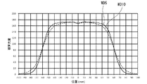
図3は、本実施形態の光照射装置10を用いて、Y軸方向に一定の速度で移動する照射対象物上に紫外光を照射したときの積算光量を示すグラフである。図3の「WD5」及び「WD10」は、照射対象物のワークディスタンス(つまり、走行位置)を示し、「WD5」は、光照射装置10から5mm離れた位置を走行する照射対象物上の積算光量を示し、「WD10」は、光照射装置10から10mm離れた位置を走行する照射対象物上の積算光量を示している。なお、図3の縦軸は、積算光量(W/cm)を示し、図3の横軸は、光照射装置10の長手方向中央を0mmとして、光照射装置10の長手方向(つまり、X軸方向)に対応する位置を示している。なお、光照射装置10のX軸方向の有効照射エリアは、±40mm(つまり、80mm)である。   FIG. 3 is a graph showing the integrated light quantity when ultraviolet light is irradiated on the irradiation target moving at a constant speed in the Y-axis direction using the light irradiation apparatus 10 of the present embodiment. “WD5” and “WD10” in FIG. 3 indicate the work distance (that is, the traveling position) of the irradiation object, and “WD5” indicates the integration on the irradiation object traveling at a position 5 mm away from the light irradiation device 10 The light amount is shown, and “WD10” is the integrated light amount on the irradiation object traveling at a position 10 mm away from the light irradiation device 10. The vertical axis in FIG. 3 indicates the integrated light quantity (W / cm), and the horizontal axis in FIG. 3 indicates the longitudinal direction center of the light irradiation apparatus 10 as 0 mm. Position corresponding to the direction). In addition, the effective irradiation area of the X-axis direction of the light irradiation apparatus 10 is +/- 40 mm (that is, 80 mm).

図3に示すように、本実施形態の光照射装置10によれば、「WD5」の位置の照射対象物上において均一度:1.9%の積算光量が得られ、「WD10」の位置の照射対象物上において均一度:4.1%の積算光量が得られる。なお、本明細書において、均一度とは、有効照射エリア内の積算光量の最大値を「MAX」とし、最小値を「MIN」としたときに、(MAX−MIN)/(MAX+MIN)×100で示される値であり、本実施形態においては、均一度(つまり、有効照射エリア内の積算光量分布のムラ)が6%未満であるときに、略均一な積算光量であると評価している。   As shown in FIG. 3, according to the light irradiation device 10 of the present embodiment, the integrated light quantity of uniformity: 1.9% is obtained on the irradiation object at the position of “WD5”, and An integrated light quantity of 4.1% is obtained on the object to be irradiated. In the present specification, uniformity is defined as (MAX−MIN) / (MAX + MIN) × 100, where “MAX” is the maximum value of integrated light quantity in the effective irradiation area and “MIN” is the minimum value. In this embodiment, when the degree of uniformity (that is, the unevenness of the integrated light amount distribution in the effective irradiation area) is less than 6%, it is evaluated as a substantially uniform integrated light amount. .

ここで、本実施形態の効果を説明するために、いくつかの比較例を示す。図4は、第1の比較例の光照射装置10Xが有するLEDモジュール210X、220Xの構成を説明する図である。また、図5は、光照射装置10Xを用いて、Y軸方向に一定の速度で移動する照射対象物上に紫外光を照射したときの積算光量を示すグラフである。   Here, in order to explain the effect of the present embodiment, some comparative examples are shown. FIG. 4 is a view for explaining the configuration of the LED modules 210X and 220X included in the light irradiation device 10X of the first comparative example. FIG. 5 is a graph showing the integrated light quantity when ultraviolet light is irradiated on the irradiation target moving at a constant speed in the Y-axis direction using the light irradiation device 10X.

図4に示すように、LEDモジュール210X、220Xにおいては、矩形状の基板202X上に、20個(X軸方向)×10列(Y軸方向)の態様で、200個のLED素子205が正方格子状(3mm×3mm)にCOB(Chip On Board)実装されている。つまり、LEDモジュール210X、220Xは、基板202Xの形状が異なると共に、LED素子205の配置密度が高い基板端部Qを備えていない点で本実施形態のLEDモジュール210、220と異なっている。そして、このような構成を採ると、連結部(つまり、継ぎ目部J)において、各LED素子205の間隔が広くなってしまうため、図5に示すように、光照射装置10Xの長手方向略中央において積算光量が落ち込み、均一にはならないことが分かる。なお、図5において、「WD5」の位置の照射対象物上の均一度は、10.3%であり、「WD10」の位置の照射対象物上の均一度は、7.1%であった。   As shown in FIG. 4, in the LED modules 210X and 220X, 200 LED elements 205 are square on the rectangular substrate 202X in a mode of 20 (X-axis direction) × 10 rows (Y-axis direction) COB (Chip On Board) is mounted in a grid (3 mm × 3 mm). That is, the LED modules 210X and 220X differ from the LED modules 210 and 220 of the present embodiment in that they do not have the substrate end Q with a different arrangement of the substrate 202X and a high arrangement density of the LED elements 205. And if such a configuration is adopted, the distance between the LED elements 205 becomes wider at the connection portion (that is, the joint portion J), and therefore, as shown in FIG. The accumulated light amount drops in the case of (3), and it can be seen that the amount of In FIG. 5, the uniformity on the irradiation object at the position of “WD5” was 10.3%, and the uniformity on the irradiation object at the position of “WD10” was 7.1%. .

図6は、第2の比較例の光照射装置10Yが有するLEDモジュール210Y、220Yの構成を説明する図である。また、図7は、光照射装置10Yを用いて、Y軸方向に一定の速度で移動する照射対象物上に紫外光を照射したときの積算光量を示すグラフである。   FIG. 6 is a diagram for explaining the configuration of the LED modules 210Y and 220Y of the light irradiation device 10Y of the second comparative example. FIG. 7 is a graph showing the integrated light quantity when ultraviolet light is irradiated on the irradiation target moving at a constant speed in the Y-axis direction using the light irradiation device 10Y.

図6に示すように、LEDモジュール210Y、220Yにおいては、平面視で略平行四辺形の平板状の基板202Y上に、20個(X軸方向)×10列(Y軸方向)の態様で、200個のLED素子205が等間隔(X軸方向:3mm、Y軸方向:3mm)にCOB(Chip On Board)実装されている。つまり、LEDモジュール210Y、220Yは、LED素子205の配置密度が高い基板端部Qを備えていない点で本実施形態のLEDモジュール210、220と異なっている。そして、このような構成を採ると、連結部(つまり、継ぎ目部J)周辺において、LED素子205の配置密度が低くなってしまうため、図7に示すように、光照射装置10Yの長手方向略中央において積算光量が落ち込み、均一にはならないことが分かる。なお、図7において、「WD5」の位置の照射対象物上の均一度は、9.0%であり、「WD10」の位置の照射対象物上の均一度は、6.2%であった。   As shown in FIG. 6, in the LED modules 210Y and 220Y, 20 (in the X-axis direction) × 10 (in the Y-axis direction) on the flat substrate 202Y having a substantially parallelogram in plan view, Two hundred LED elements 205 are COB (Chip On Board) mounted at equal intervals (X-axis direction: 3 mm, Y-axis direction: 3 mm). That is, the LED modules 210Y and 220Y are different from the LED modules 210 and 220 of the present embodiment in that the substrate end Q having a high arrangement density of the LED elements 205 is not provided. And if such a configuration is adopted, the arrangement density of the LED elements 205 becomes low around the connection portion (that is, the joint portion J), and therefore, as shown in FIG. It can be seen that the integrated light quantity drops at the center and is not uniform. In FIG. 7, the uniformity on the irradiation object at the position of “WD5” was 9.0%, and the uniformity on the irradiation object at the position of “WD10” was 6.2%. .

以上説明したように、本実施形態の構成においては、LEDモジュール210、220の各基板202の形状を略平行四辺形とし、各基板202の斜辺と隣接する基板202の斜辺とが係合するように配置されると共に、各基板202の基板端部QにおけるLED素子205のX軸方向の配置密度を基板中央部PにおけるLED素子205のX軸方向の配置密度よりも高くなるように構成している。そして、2つのLEDモジュール210、220がX軸方向に連結されたときに、各基板202の基板端部Qが継ぎ目部Jを挟んで隣接している領域(つまり、図2の基板隣接部R)における、LED素子205の配置密度が、各基板202の基板中央部Pにおける、LED素子205の配置密度と略等しくなるように構成されている。このため、本実施形態の光照射装置10を用いて、Y軸方向に一定の速度で移動する照射対象物上に紫外光を照射すると、照射対象物上において、略均一な積算光量が得られる。   As described above, in the configuration of the present embodiment, the shapes of the substrates 202 of the LED modules 210 and 220 are substantially parallelograms, and the oblique sides of the respective substrates 202 are engaged with the oblique sides of the adjacent substrates 202. And the arrangement density of the LED elements 205 at the substrate end Q of each substrate 202 in the X-axis direction is higher than the arrangement density of the LED elements 205 at the substrate central portion P in the X-axis direction. There is. Then, when the two LED modules 210 and 220 are connected in the X-axis direction, the substrate end Q of each substrate 202 is adjacent to each other across the joint portion J (that is, the substrate adjacent portion R in FIG. , The arrangement density of the LED elements 205 is approximately equal to the arrangement density of the LED elements 205 at the substrate central portion P of each substrate 202. Therefore, when the irradiation object moving at a constant speed in the Y-axis direction is irradiated with ultraviolet light using the light irradiation device 10 of the present embodiment, a substantially uniform integrated light amount can be obtained on the irradiation object .

以上が本実施形態の説明であるが、本発明は、上記の構成に限定されるものではなく、本発明の技術的思想の範囲内において様々な変形が可能である。   The above is the description of the present embodiment, but the present invention is not limited to the above configuration, and various modifications are possible within the scope of the technical idea of the present invention.

例えば、本実施形態の基板202は、平面視で略平行四辺形の形状を呈するものとして説明したが、このような構成に限定されるものではなく、2つの基板202をX軸方向に沿って繋ぎ合わせたときに、2つの基板202が係合し、各基板202の基板端部Qが継ぎ目部Jを挟んでX軸方向及びY軸方向に連続するような形状であればよい。   For example, although the substrate 202 according to the present embodiment has been described as having a substantially parallelogram shape in a plan view, the present invention is not limited to such a configuration, and two substrates 202 along the X axis direction The two substrates 202 may be engaged when they are joined, and the substrate end portions Q of the respective substrates 202 may be shaped so as to be continuous in the X axis direction and the Y axis direction across the joint portion J.

また、本実施形態においては、2つのLEDモジュール210、220がX軸方向に連結されるものとして説明したが、かかる構成に限定されるものではなく、さらに多くのLEDモジュールがX軸方向に連結されてもよい。   Further, in the present embodiment, the two LED modules 210 and 220 are described as being coupled in the X-axis direction. However, the present invention is not limited to this configuration, and more LED modules are coupled in the X-axis direction. It may be done.

(第2の実施形態)
図8は、本発明の第2の実施形態に係る光照射装置10Aの構成を示す図である。なお、説明の便宜のため、図8においては、LEDモジュール210A、220Aのみを示し、その他の構成は省略している。
Second Embodiment
FIG. 8 is a view showing a configuration of a light irradiation device 10A according to a second embodiment of the present invention. In addition, in FIG. 8, only the LED modules 210 </ b> A and 220 </ b> A are shown for the convenience of description, and the other configuration is omitted.

図8に示すように、本実施形態の光照射装置10Aは、LEDモジュール210A、220Aの各基板202Aが、くの字状に突出する凸部202Aaと、凸部202Aaを補完するように、くの字状に窪む凹部202Abを有する点で第1の実施形態の光照射装置10と異なり、LEDモジュール210Aの基板202Aの凸部202AaがLEDモジュール220Aの基板202Aの凹部202Abと係合するように配置されて固定されている。そして、LEDモジュール210A、220Aの各列(1)〜(10)のLED素子205が、継ぎ目部Jを挟んで(つまり、LED素子205の間隔が部分的に広くなって)、X軸方向に連続するように配置されている。なお、本実施形態においては、列(1)、(10)のLED素子205は、X軸方向において同じ位置に配置され、また、列(2)、(9)のLED素子205はX軸方向において同じ位置に配置され、列(1)、(10)のLED素子205に対してX軸方向にシフトしている。また、列(3)、(8)のLED素子205は、X軸方向において同じ位置に配置され、列(2)、(9)のLED素子205に対してX軸方向にシフトしている。また、列(4)、(7)のLED素子205は、X軸方向において同じ位置に配置され、列(3)、(8)のLED素子205に対してX軸方向にシフトしている。また、列(5)、(6)のLED素子205は、X軸方向において同じ位置に配置され、列(4)、(7)のLED素子205に対してX軸方向にシフトしている。そして、本実施形態の各LED素子205は、Y軸方向においても整列しており、Y軸方向に10個のLED素子205が並ぶ領域(基板中央部P)のLED素子205(図8において、白色の□(白抜き四角)で示すLED素子205)は、X軸方向に略3mmの間隔で配置されており、Y軸方向に10個よりも少ないLED素子205が並ぶ領域(基板端部Q)のLED素子205(図8において、黒色の■(黒塗り四角)で示すLED素子205)は、X軸方向に略2.5mmの間隔で配置されている。つまり、基板端部QにおけるLED素子205のX軸方向の配置密度が、基板中央部PにおけるLED素子205のX軸方向の配置密度よりも高くなるように構成している。そして、2つのLEDモジュール210A、220Aが継ぎ目部Jを挟んで隣接している領域(つまり、図8の基板隣接部R)における、LED素子205の配置密度は、60個(基板隣接部RのLED素子205の数)/15mm(基板隣接部Rの幅)となり、各LEDモジュール210A、220Aの基板中央部Pにおける、LED素子205の配置密度(基板中央部Pにおける15mmあたりのLED素子205の数:60個)と略等しくなるように設定されている。つまり、本実施形態においても、第1の実施形態と同様、LEDモジュール210A、220Aの各基板202Aが係合するように配置されると共に、各基板202Aの基板端部QにおけるLED素子205のX軸方向の配置密度を基板中央部PにおけるLED素子205のX軸方向の配置密度よりも高くなるように構成している。そして、2つのLEDモジュール210A、220AがX軸方向に連結されたときに、各基板202Aの基板端部Qが継ぎ目部Jを挟んで隣接している領域(つまり、図8の基板隣接部R)における、LED素子205の配置密度が、各基板202Aの基板中央部Pにおける、LED素子205の配置密度と略等しくなるように構成されている。このため、本実施形態の光照射装置10Aを用いて、Y軸方向に一定の速度で移動する照射対象物上に紫外光を照射すると、照射対象物上において、略均一な積算光量が得られる。   As shown in FIG. 8, in the light irradiation device 10A of the present embodiment, each substrate 202A of the LED modules 210A and 220A has a convex portion 202Aa that protrudes in a V shape and a convex portion 202Aa. Unlike the light irradiation device 10 of the first embodiment in that the concave portion 202Ab of the LED module is recessed, the convex portion 202Aa of the substrate 202A of the LED module 210A engages with the concave portion 202Ab of the substrate 202A of the LED module 220A. Placed and fixed. Then, the LED elements 205 of each row (1) to (10) of the LED modules 210A and 220A sandwich the joint portion J (that is, the distance between the LED elements 205 is partially widened) in the X axis direction It is arranged to be continuous. In the present embodiment, the LED elements 205 in the rows (1) and (10) are arranged at the same position in the X-axis direction, and the LED elements 205 in the rows (2) and (9) are in the X-axis direction At the same position and shifted in the X-axis direction with respect to the LED elements 205 of the rows (1) and (10). Further, the LED elements 205 in the rows (3) and (8) are arranged at the same position in the X-axis direction, and are shifted in the X-axis direction with respect to the LED elements 205 in the rows (2) and (9). The LED elements 205 in the rows (4) and (7) are arranged at the same position in the X-axis direction, and shifted in the X-axis direction with respect to the LED elements 205 in the rows (3) and (8). The LED elements 205 in the rows (5) and (6) are arranged at the same position in the X-axis direction, and shifted in the X-axis direction with respect to the LED elements 205 in the rows (4) and (7). And each LED element 205 of this embodiment is aligned also in the Y-axis direction, and in the area (substrate center P) where ten LED elements 205 are arranged in the Y-axis direction (in FIG. 8) LED elements 205 shown by white squares (open squares) are arranged at intervals of about 3 mm in the X-axis direction, and a region (substrate end Q) in which less than ten LED elements 205 are arranged in the Y-axis direction The LED elements 205) (LED elements 205 shown by black squares (black squares) in FIG. 8) are arranged at an interval of about 2.5 mm in the X-axis direction. That is, the arrangement density of the LED elements 205 at the substrate end Q in the X-axis direction is higher than the arrangement density of the LED elements 205 at the substrate center P in the X-axis direction. The arrangement density of the LED elements 205 in the region where the two LED modules 210A and 220A are adjacent to each other across the joint portion J (that is, the substrate adjacent portion R in FIG. 8) is 60 (substrate adjacent portion R). The number of LED elements 205/15 mm (the width of the substrate adjacent portion R), and the arrangement density of the LED elements 205 in the substrate central portion P of each LED module 210A, 220 A (15 mm of the LED devices 205 in the substrate central portion P The number is set to be approximately equal to 60). That is, also in the present embodiment, as in the first embodiment, the respective substrates 202A of the LED modules 210A and 220A are arranged to be engaged, and X of the LED elements 205 at the substrate end Q of the respective substrates 202A. The arrangement density in the axial direction is configured to be higher than the arrangement density in the X-axis direction of the LED elements 205 at the substrate central portion P. Then, when the two LED modules 210A and 220A are connected in the X-axis direction, a region where the substrate end Q of each substrate 202A is adjacent to each other across the joint portion J (that is, the substrate adjacent portion R in FIG. , The arrangement density of the LED elements 205 is approximately equal to the arrangement density of the LED elements 205 at the substrate central portion P of each substrate 202A. Therefore, when the irradiation object moving at a constant speed in the Y-axis direction is irradiated with ultraviolet light using the light irradiation device 10A of the present embodiment, a substantially uniform integrated light amount can be obtained on the irradiation object .

図9は、本実施形態の光照射装置10Aを用いて、Y軸方向に一定の速度で移動する照射対象物上に紫外光を照射したときの積算光量を示すグラフである。図9に示すように、本実施形態の光照射装置10Aによれば、「WD5」の位置の照射対象物上において均一度:3.8%の積算光量が得られ、「WD10」の位置の照射対象物上において均一度:5.0%の積算光量が得られる。   FIG. 9 is a graph showing the integrated light quantity when ultraviolet light is irradiated on the irradiation target moving at a constant speed in the Y-axis direction using the light irradiation device 10A of the present embodiment. As shown in FIG. 9, according to the light irradiation device 10A of the present embodiment, the integrated light quantity of uniformity: 3.8% is obtained on the irradiation object at the position of “WD5”, and the light emission device 10A of the position of “WD10” An integrated light quantity of 5.0% uniformity can be obtained on the object to be irradiated.

(第3の実施形態)
図10は、本発明の第3の実施形態に係る光照射装置10Bの構成を示す図である。なお、説明の便宜のため、図10においては、LEDモジュール210B、220Bのみを示し、その他の構成は省略している。
Third Embodiment
FIG. 10 is a view showing a configuration of a light irradiation device 10B according to a third embodiment of the present invention. In addition, in FIG. 10, only LED module 210B, 220B is shown for the facilities of description, and the other structure is abbreviate | omitted.

図10に示すように、本実施形態の光照射装置10Bは、LEDモジュール210B、220Bの各基板202Bが、階段状に突出する凸部202Baと、凸部202Baを補完するように、階段状に窪む凹部202Bbを有する点で第1の実施形態の光照射装置10と異なり、LEDモジュール210Bの基板202Bの凸部202BaがLEDモジュール220Bの基板202Bの凹部202Bbと係合するように配置されて固定されている。そして、LEDモジュール210B、220Bの各列(1)〜(10)のLED素子205が、継ぎ目部Jを挟んで(つまり、LED素子205の間隔が部分的に広くなって)、X軸方向に連続するように配置されている。なお、本実施形態においては、列(1)〜(5)のLED素子205は、X軸方向において同じ位置に配置され、また、列(6)〜(10)のLED素子205はX軸方向において同じ位置に配置され、列(1)〜(5)のLED素子205に対してX軸方向にシフトしている。そして、本実施形態の各LED素子205は、Y軸方向においても整列しており、Y軸方向に10個のLED素子205が並ぶ領域(基板中央部P)のLED素子205(図10において、白色の□(白抜き四角)で示すLED素子205)は、X軸方向に略3mmの間隔で配置されており、Y軸方向に10個よりも少ないLED素子205が並ぶ領域(基板端部Q)のLED素子205(図10において、黒色の■(黒塗り四角)で示すLED素子205)は、X軸方向に略2.5mmの間隔で配置されている。また、本実施形態の基板隣接部RのLED素子205は、Y軸方向の間隔が2.5mmとなるように配置されている。つまり、基板端部QにおけるLED素子205のX軸方向及びY軸方向の配置密度が、基板中央部PにおけるLED素子205のX軸方向及びY軸方向の配置密度よりも高くなるように構成している。そして、2つのLEDモジュール210B、220Bの基板端部Qが継ぎ目部Jを挟んで隣接している領域(つまり、図10の基板隣接部R)における、LED素子205の配置密度は、60個(基板隣接部RのLED素子205の数)/15mm(基板隣接部Rの幅)となり、各LEDモジュール210、220の基板中央部Pにおける、LED素子205の配置密度(基板中央部Pにおける15mmあたりのLED素子205の数:60個)と略等しくなるように設定されている。つまり、本実施形態においても、第1の実施形態と同様、LEDモジュール210B、220Bの各基板202Bが係合するように配置されると共に、各基板202Bの基板端部QにおけるLED素子205の配置密度が、基板中央部PにおけるLED素子205の配置密度よりも高くなるように構成している。そして、2つのLEDモジュール210B、220BがX軸方向に連結されたときに、各基板202Bの基板端部Qが継ぎ目部Jを挟んで隣接している領域(つまり、図10の基板隣接部R)における、LED素子205の配置密度が、各基板202Bの基板中央部Pにおける、LED素子205の配置密度と略等しくなるように構成されている。このため、本実施形態の光照射装置10Bを用いて、Y軸方向に一定の速度で移動する照射対象物上に紫外光を照射すると、照射対象物上において、略均一な積算光量が得られる。   As shown in FIG. 10, in the light irradiation device 10B of the present embodiment, each substrate 202B of the LED modules 210B and 220B has a step shape so as to complement the protrusion 202Ba and the protrusion 202Ba protruding in a step shape. Unlike the light irradiation device 10 of the first embodiment in that the concave portion 202Bb is recessed, the convex portion 202Ba of the substrate 202B of the LED module 210B is arranged to engage with the concave portion 202Bb of the substrate 202B of the LED module 220B. It is fixed. Then, the LED elements 205 of each row (1) to (10) of the LED modules 210B and 220B sandwich the joint portion J (that is, the distance between the LED elements 205 is partially widened) in the X axis direction It is arranged to be continuous. In the present embodiment, the LED elements 205 in the rows (1) to (5) are arranged at the same position in the X-axis direction, and the LED elements 205 in the rows (6) to (10) are in the X-axis direction , And are shifted in the X-axis direction with respect to the LED elements 205 in the rows (1) to (5). The LED elements 205 of this embodiment are also aligned in the Y-axis direction, and the LED elements 205 (in FIG. 10, in a region (substrate central portion P) in which ten LED elements 205 are arranged in the Y-axis direction. LED elements 205 shown by white squares (open squares) are arranged at intervals of about 3 mm in the X-axis direction, and a region (substrate end Q) in which less than ten LED elements 205 are arranged in the Y-axis direction The LED elements 205) (LED elements 205 indicated by black squares (black squares) in FIG. 10) are arranged at intervals of about 2.5 mm in the X-axis direction. In addition, the LED elements 205 of the substrate adjacent portion R of the present embodiment are arranged so that the distance in the Y-axis direction is 2.5 mm. That is, the arrangement density of the LED elements 205 in the X axis direction and the Y axis direction at the substrate end Q is higher than the arrangement density in the X axis direction and the Y axis direction of the LED elements 205 at the substrate center P ing. The arrangement density of the LED elements 205 is 60 (in the area where the substrate ends Q of the two LED modules 210B and 220B are adjacent to each other across the joint portion J (that is, the substrate adjacent portion R in FIG. 10). The number of LED elements 205 in the board adjacent part R) / 15 mm (width of the board adjacent part R), and the arrangement density of the LED elements 205 in the board center part P of each LED module 210, 220 (about 15 mm in the board center part P) The number of LED elements 205: 60) is set to be approximately equal. That is, also in the present embodiment, as in the first embodiment, the respective substrates 202B of the LED modules 210B and 220B are arranged to be engaged, and the arrangement of the LED elements 205 at the substrate end Q of the respective substrates 202B. The density is configured to be higher than the arrangement density of the LED elements 205 at the substrate central portion P. Then, when the two LED modules 210B and 220B are connected in the X-axis direction, a region where the substrate end Q of each substrate 202B is adjacent to each other across the joint portion J (that is, the substrate adjacent portion R in FIG. , The arrangement density of the LED elements 205 is approximately equal to the arrangement density of the LED elements 205 at the substrate central portion P of each substrate 202B. For this reason, when the ultraviolet light is irradiated on the irradiation target moving at a constant speed in the Y-axis direction using the light irradiation device 10B of the present embodiment, a substantially uniform integrated light amount can be obtained on the irradiation target .

図11は、本実施形態の光照射装置10Bを用いて、Y軸方向に一定の速度で移動する照射対象物上に紫外光を照射したときの積算光量を示すグラフである。図11に示すように、本実施形態の光照射装置10Bによれば、「WD5」の位置の照射対象物上において均一度:5.2%の積算光量が得られ、「WD10」の位置の照射対象物上において均一度:4.0%の積算光量が得られる。   FIG. 11 is a graph showing the integrated light quantity when ultraviolet light is irradiated on the irradiation target moving at a constant speed in the Y-axis direction using the light irradiation device 10B of the present embodiment. As shown in FIG. 11, according to the light irradiation device 10B of the present embodiment, the integrated light quantity of uniformity: 5.2% is obtained on the irradiation object at the position of “WD5”, and the light emission device 10B at the position of “WD10” An integrated light quantity of 4.0% uniformity can be obtained on the object to be irradiated.

(第4の実施形態)
図12は、本発明の第4の実施形態に係る光照射装置10Cの構成を示す図である。なお、説明の便宜のため、図12においては、LEDモジュール210C、220Cのみを示し、その他の構成は省略している。
Fourth Embodiment
FIG. 12 is a view showing a configuration of a light irradiation device 10C according to a fourth embodiment of the present invention. In addition, in FIG. 12, only the LED modules 210C and 220C are shown for the convenience of description, and the other structure is abbreviate | omitted.

図12に示すように、本実施形態の光照射装置10Cは、LEDモジュール210C、220Cの各基板202Cの斜辺の角度が大きく、各基板202C上に、20個(X軸方向)×20列(Y軸方向)の態様で、400個のLED素子205がCOB(Chip On Board)実装されている点で第1の実施形態の光照射装置10と異なる。そして、LEDモジュール210C、220Cの各列(1)〜(20)のLED素子205が、継ぎ目部Jを挟んで(つまり、LED素子205の間隔が部分的に広くなって)、X軸方向に連続するように配置されている。なお、本実施形態においては、列(1)〜(4)のLED素子205は、X軸方向において同じ位置に配置され、また、列(5)〜(8)のLED素子205はX軸方向において同じ位置に配置され、列(1)〜(4)のLED素子205に対してX軸方向にシフトしている。また、列(9)〜(12)のLED素子205は、X軸方向において同じ位置に配置され、列(5)〜(8)のLED素子205に対してX軸方向にシフトしている。また、列(13)〜(16)のLED素子205は、X軸方向において同じ位置に配置され、列(9)〜(12)のLED素子205に対してX軸方向にシフトしている。また、列(17)〜(20)のLED素子205は、X軸方向において同じ位置に配置され、列(13)〜(16)のLED素子205に対してX軸方向にシフトしている。そして、本実施形態の各LED素子205は、Y軸方向においても整列しており、Y軸方向に20個のLED素子205が並ぶ領域(基板中央部P)のLED素子205(図12において、白色の□(白抜き四角)で示すLED素子205)は、X軸方向に略3mmの間隔で配置されており、Y軸方向に20個よりも少ないLED素子205が並ぶ領域(基板端部Q)のLED素子205(図12において、黒色の■(黒塗り四角)で示すLED素子205)は、X軸方向に略2.14mmの間隔で配置されている。つまり、基板端部QにおけるLED素子205のX軸方向の配置密度が、基板中央部PにおけるLED素子205のX軸方向の配置密度よりも高くなるように構成している。そして、2つのLEDモジュール210C、220Cが継ぎ目部Jを挟んで隣接している領域(つまり、図12の基板隣接部R)における、LED素子205の配置密度は、120個(基板隣接部RのLED素子205の数)/約15mm(基板隣接部Rの幅)となり、各LEDモジュール210C、220Cの基板中央部Pにおける、LED素子205の配置密度(基板中央部Pにおける15mmあたりのLED素子205の数:120個)と略等しくなるように設定されている。つまり、本実施形態においても、第1の実施形態と同様、LEDモジュール210C、220Cの各基板202Cが係合するように配置されると共に、各基板202Cの基板端部QにおけるLED素子205のX軸方向の配置密度が、基板中央部PにおけるLED素子205のX軸方向の配置密度よりも高くなるように構成している。そして、2つのLEDモジュール210C、220CがX軸方向に連結されたときに、各基板202Cの基板端部Qが継ぎ目部Jを挟んで隣接している領域(つまり、図12の基板隣接部R)における、LED素子205の配置密度が、各基板202Cの基板中央部Pにおける、LED素子205の配置密度と略等しくなるように構成されている。このため、本実施形態の光照射装置10Cを用いて、Y軸方向に一定の速度で移動する照射対象物上に紫外光を照射すると、照射対象物上において、略均一な積算光量が得られる。   As shown in FIG. 12, in the light irradiation device 10C of the present embodiment, the angle of the oblique side of each substrate 202C of the LED modules 210C and 220C is large, and 20 pieces (X axis direction) × 20 rows on each substrate 202C. It differs from the light irradiation device 10 of the first embodiment in that 400 LED elements 205 are mounted on a chip on board (COB) in the aspect of Y axis direction). Then, the LED elements 205 of each row (1) to (20) of the LED modules 210C and 220C sandwich the joint portion J (that is, the distance between the LED elements 205 is partially widened) in the X axis direction It is arranged to be continuous. In the present embodiment, the LED elements 205 in the rows (1) to (4) are arranged at the same position in the X-axis direction, and the LED elements 205 in the rows (5) to (8) are in the X-axis direction , And are shifted in the X-axis direction with respect to the LED elements 205 of the rows (1) to (4). Further, the LED elements 205 in the rows (9) to (12) are arranged at the same position in the X-axis direction, and shifted in the X-axis direction with respect to the LED elements 205 in the rows (5) to (8). Further, the LED elements 205 in the rows (13) to (16) are arranged at the same position in the X-axis direction, and shifted in the X-axis direction with respect to the LED elements 205 in the rows (9) to (12). Further, the LED elements 205 in the rows (17) to (20) are arranged at the same position in the X-axis direction, and are shifted in the X-axis direction with respect to the LED elements 205 in the rows (13) to (16). The LED elements 205 according to the present embodiment are also aligned in the Y-axis direction, and the LED elements 205 (in FIG. 12, in the central portion P of the substrate) where 20 LED elements 205 are arranged in the Y-axis direction. LED elements 205 shown by white squares (open squares) are arranged at intervals of approximately 3 mm in the X-axis direction, and a region (substrate end Q) in which less than 20 LED elements 205 are arranged in the Y-axis direction The LED elements 205) (LED elements 205 shown by black squares (black squares) in FIG. 12) are arranged at intervals of approximately 2.14 mm in the X-axis direction. That is, the arrangement density of the LED elements 205 at the substrate end Q in the X-axis direction is higher than the arrangement density of the LED elements 205 at the substrate center P in the X-axis direction. The arrangement density of the LED elements 205 in the region where the two LED modules 210C and 220C are adjacent to each other across the joint portion J (that is, the substrate adjacent portion R in FIG. 12) is 120 (substrate adjacent portion R). The number of LED elements 205 / about 15 mm (the width of the substrate adjacent part R), and the arrangement density of the LED elements 205 at the substrate central part P of each LED module 210C, 220C (LED elements 205 per 15 mm in the substrate central part P (Number of 120) is set to be approximately equal to That is, also in the present embodiment, as in the first embodiment, the respective substrates 202C of the LED modules 210C and 220C are arranged to be engaged, and X of the LED elements 205 at the substrate end Q of the respective substrates 202C. The arrangement density in the axial direction is configured to be higher than the arrangement density in the X-axis direction of the LED elements 205 at the substrate central portion P. Then, when the two LED modules 210C and 220C are connected in the X-axis direction, a region where the substrate end Q of each substrate 202C is adjacent to each other across the joint portion J (that is, the substrate adjacent portion R in FIG. 12) , The arrangement density of the LED elements 205 is substantially equal to the arrangement density of the LED elements 205 at the substrate central portion P of each substrate 202C. For this reason, when the ultraviolet light is irradiated on the irradiation target moving at a constant speed in the Y-axis direction using the light irradiation device 10C of the present embodiment, a substantially uniform integrated light amount can be obtained on the irradiation target .

図13は、本実施形態の光照射装置10Cを用いて、Y軸方向に一定の速度で移動する照射対象物上に紫外光を照射したときの積算光量を示すグラフである。図13に示すように、本実施形態の光照射装置10Cによれば、「WD5」の位置の照射対象物上において均一度:4.4%の積算光量が得られ、「WD10」の位置の照射対象物上において均一度:5.3%の積算光量が得られる。   FIG. 13 is a graph showing the integrated light quantity when ultraviolet light is irradiated on the irradiation target moving at a constant speed in the Y-axis direction using the light irradiation device 10C of the present embodiment. As shown in FIG. 13, according to the light irradiation device 10C of the present embodiment, the integrated light quantity of uniformity: 4.4% is obtained on the irradiation object at the position of “WD5”, and the light emission device 10C at the position of “WD10” An integrated light quantity of 5.3% is obtained on the object to be irradiated.

なお、本実施形態においては、LED素子205が20個(X軸方向)×20列(Y軸方向)の態様で並び、第1の実施形態においては、LED素子205が20個(X軸方向)×10列(Y軸方向)の態様で並ぶものとして説明したが、本発明は、かかる構成に限定されるものではなく、基板隣接部Rが形成される限りにおいて、X軸方向にN個(Nは4以上の整数)、Y軸方向にM個(Mは2以上の整数)の態様で並べばよい。   In the present embodiment, the LED elements 205 are arranged in the form of 20 pieces (X-axis direction) × 20 rows (Y-axis direction), and in the first embodiment, 20 pieces of LED elements 205 (X-axis direction) The present invention is not limited to this configuration, but N in the X-axis direction as long as the substrate adjacent portion R is formed. (N is an integer of 4 or more), and may be arranged in the form of M (M is an integer of 2 or more) in the Y-axis direction.

また、第1乃至第4の実施形態において、基板中央部PのLED素子205は、正方格子状に配置されるものとしたが、本発明は、かかる構成に限定されるものではなく、略一様な配置密度となるように配置されればよい。   In the first to fourth embodiments, the LED elements 205 in the central portion P of the substrate are arranged in a square grid shape, but the present invention is not limited to this configuration, and substantially It should just be arrange | positioned so that it may become an arrangement | positioning density.

また、第1乃至第4の実施形態において、基板端部QのLED素子205は、X軸方向及びY軸方向に所定の間隔をおいて配置されるものとしたが、本発明は、かかる構成に限定されるものではなく、各基板がX軸方向に連結されたときに、各基板の基板端部Qが継ぎ目部Jを挟んで隣接している領域(つまり、基板隣接部R)において、略一様な配置密度となるように配置されればよい。   In the first to fourth embodiments, the LED elements 205 at the substrate end Q are arranged at predetermined intervals in the X-axis direction and the Y-axis direction, but the present invention In the region where the substrate ends Q of the respective substrates are adjacent to each other across the joint portion J (that is, the substrate adjacent portions R) when the respective substrates are connected in the X-axis direction, It may be arranged to have a substantially uniform arrangement density.

なお、今回開示された実施の形態は、全ての点で例示であって、制限的なものではないと考えられるべきである。本発明の範囲は、上記した説明ではなく、特許請求の範囲によって示され、特許請求の範囲と均等の意味及び範囲内での全ての変更が含まれることが意図される。   It should be understood that the embodiment disclosed this time is illustrative in all points and not restrictive. The scope of the present invention is shown not by the above description but by the scope of the claims, and is intended to include all modifications within the scope and meaning equivalent to the scope of the claims.

10、10A、10B、10C、10X、10Y 光照射装置
100 ベースプレート
202 基板
202Aa、202Ba 凸部
202Ab、202Bb 凹部
205 LED素子
210、220、210A、220A、210B、220B、210C、220C LEDモジュール
10, 10A, 10B, 10C, 10X, 10Y Light irradiation apparatus 100 Base plate 202 Base plate 202Aa, 202Ba Convex part 202Ab, 202Bb Concave part 205 LED element 210, 220, 210A, 220A, 210B, 220B, 210C, 220C LED module

Claims (9)

第1方向に相対的に移動する照射対象物上に、前記第1方向と直交する第2方向に延び、かつ、前記第1方向に所定の線幅を有するライン状の光を照射する光照射装置であって、
少なくとも前記第2方向に平行な2辺を有し、前記第1方向及び前記第2方向で規定される平板状の基板と、前記基板の表面に配置され、前記光を出射する複数の光源と、をそれぞれ有し、前記第2方向に連結するように配置された複数の光照射モジュールを備え、
前記各基板は、前記複数の光源が前記第1方向及び前記第2方向に第1の密度で配列される基板中央部と、前記複数の光源が少なくとも前記第2方向において前記第1の密度よりも高い第2の密度で配列される基板端部と、からなり、
前記各基板の前記基板端部は、前記第2方向に隣接する基板の前記基板端部と連結可能な形状を呈し、前記第2方向に隣接する基板の前記基板端部と連結したときに、前記第1方向及び前記第2方向に連続して、基板隣接部を形成し、
前記基板隣接部の前記複数の光源の密度が、前記基板中央部の前記複数の光源の密度と略等しい
ことを特徴とする光照射装置。
Light irradiation for irradiating line-shaped light extending in a second direction orthogonal to the first direction and having a predetermined line width in the first direction on an irradiation object relatively moving in a first direction A device,
A flat substrate having at least two sides parallel to the second direction and defined by the first direction and the second direction , and a plurality of light sources disposed on the surface of the substrate and emitting the light , And are provided with a plurality of light irradiation modules arranged to be connected in the second direction,
In each of the substrates, a substrate central portion in which the plurality of light sources are arranged at a first density in the first direction and the second direction, and the first density in at least the second direction of the plurality of light sources And the substrate end arranged at a high second density,
The substrate end of each substrate has a shape connectable to the substrate end of the substrate adjacent in the second direction, and when connected to the substrate end of the substrate adjacent in the second direction, A substrate adjacent portion is formed continuously in the first direction and the second direction ,
A light irradiation apparatus characterized in that the density of the plurality of light sources adjacent to the substrate is substantially equal to the density of the plurality of light sources in the central portion of the substrate.
前記基板中央部において、前記複数の光源は、前記第1方向に沿って第1の間隔をおいてM個(Mは2以上の整数)並び、前記第2方向に沿って第2の間隔をおいてN個(Nは4以上の整数)並び、
前記基板隣接部において、前記複数の光源は、前記第2方向に沿って前記第2の間隔よりも狭い第3の間隔をおいて並ぶ
ことを特徴とする請求項1に記載の光照射装置。
In the central portion of the substrate, M light sources (M is an integer of 2 or more) are arranged at a first spacing along the first direction, and a second spacing is formed along the second direction. Where N (N is an integer of 4 or more)
2. The light irradiation apparatus according to claim 1, wherein the plurality of light sources are arranged at a third distance narrower than the second distance along the second direction at the substrate adjacent part. 3.
前記基板隣接部において、前記複数の光源は、前記第1方向に沿って前記第1の間隔をおいて並ぶことを特徴とする請求項2に記載の光照射装置。   The light irradiation apparatus according to claim 2, wherein the plurality of light sources are arranged at the first interval along the first direction at the substrate adjacent portion. 前記基板隣接部において、前記複数の光源は、前記第1方向に沿って前記第1の間隔よりも狭い第4の間隔をおいて並ぶことを特徴とする請求項2に記載の光照射装置。   The light irradiation apparatus according to claim 2, wherein the plurality of light sources are arranged at a fourth interval narrower than the first interval along the first direction at the substrate adjacent portion. 前記各基板の前記基板端部と隣接する基板の前記基板端部との間に、前記光源が配置されない接合部を有し、前記各基板の前記基板端部が前記接合部を介して隣接する基板の前記基板端部と連結することを特徴とする請求項1から請求項のいずれか一項に記載の光照射装置。 Between the substrate end of each substrate and the substrate end of the adjacent substrate, there is a joint where the light source is not disposed, and the substrate end of each substrate is adjacent via the joint. The light irradiation device according to any one of claims 1 to 4 , wherein the light irradiation device is connected to the substrate end of the substrate. 前記接合部が、前記第1方向に対して傾斜していることを特徴とする請求項に記載の光照射装置。 The light irradiation apparatus according to claim 5 , wherein the bonding portion is inclined with respect to the first direction. 前記各基板の形状が平行四辺形であることを特徴とする請求項に記載の光照射装置。 The light irradiation apparatus according to claim 6 , wherein the shape of each of the substrates is a parallelogram. 前記接合部が、階段状に形成されていることを特徴とする請求項に記載の光照射装置。 The light irradiation apparatus according to claim 5 , wherein the joint portion is formed in a step shape. 前記接合部が、くの字状に形成されていることを特徴とする請求項に記載の光照射装置。 The light irradiation apparatus according to claim 5 , wherein the joint portion is formed in a V shape.
JP2016165194A 2016-08-25 2016-08-25 Light irradiation device Active JP6533501B2 (en)

Priority Applications (1)

Application Number Priority Date Filing Date Title
JP2016165194A JP6533501B2 (en) 2016-08-25 2016-08-25 Light irradiation device

Applications Claiming Priority (1)

Application Number Priority Date Filing Date Title
JP2016165194A JP6533501B2 (en) 2016-08-25 2016-08-25 Light irradiation device

Publications (2)

Publication Number Publication Date
JP2018032799A JP2018032799A (en) 2018-03-01
JP6533501B2 true JP6533501B2 (en) 2019-06-19

Family

ID=61303673

Family Applications (1)

Application Number Title Priority Date Filing Date
JP2016165194A Active JP6533501B2 (en) 2016-08-25 2016-08-25 Light irradiation device

Country Status (1)

Country Link
JP (1) JP6533501B2 (en)

Families Citing this family (1)

* Cited by examiner, † Cited by third party
Publication number Priority date Publication date Assignee Title
EP3761764A4 (en) 2018-02-27 2021-12-01 Mitsubishi Materials Corporation Insulating circuit board

Family Cites Families (11)

* Cited by examiner, † Cited by third party
Publication number Priority date Publication date Assignee Title
JP3612850B2 (en) * 1996-03-28 2005-01-19 富士ゼロックス株式会社 Photoelectric conversion element array device, light source device using semiconductor light emitting element array, and manufacturing method thereof
JPH11330656A (en) * 1998-05-18 1999-11-30 Seiko Precision Inc Joint structure for printed board
JP2000091646A (en) * 1998-09-17 2000-03-31 Oki Electric Ind Co Ltd Led array
JP2000289250A (en) * 1999-04-13 2000-10-17 Oki Data Corp Led array chip and led array print head
JP2002333847A (en) * 2001-05-10 2002-11-22 Mitsubishi Electric Engineering Co Ltd Led display
JP5228502B2 (en) * 2008-01-23 2013-07-03 凸版印刷株式会社 Unit surface light source light emitter element, surface light source light emitter unit, backlight unit, illumination device, and display device
JP2013254630A (en) * 2012-06-06 2013-12-19 Panasonic Corp Led unit and lighting fixture
JP2014090055A (en) * 2012-10-30 2014-05-15 Kyocera Corp Light irradiation module and printer
KR101319360B1 (en) * 2013-03-04 2013-10-16 유버 주식회사 Chip on board type uv led package and method for making the same
JP6208563B2 (en) * 2013-11-28 2017-10-04 国立大学法人 東京大学 UV irradiation equipment
JP5907291B1 (en) * 2015-02-26 2016-04-26 ウシオ電機株式会社 Light irradiation element and line light irradiation device

Also Published As

Publication number Publication date
JP2018032799A (en) 2018-03-01

Similar Documents

Publication Publication Date Title
CN107388213B (en) Heat dissipation device and light irradiation device with same
US10119759B2 (en) Heat radiating apparatus and light illuminating apparatus with the same
JP6640544B2 (en) Light emitting module, lamp and circuit board for light emitting element
US10317067B2 (en) Heat radiating apparatus and light illuminating apparatus with the same
JP2017170616A (en) Light irradiation device
JP6675151B2 (en) Light irradiation device
JP5257308B2 (en) Light irradiation device
JP7128433B2 (en) Light irradiation device
JP6533501B2 (en) Light irradiation device
US9625119B2 (en) Non-uniform lens array for illumination profile modification
JP6411572B1 (en) Light emitting device and light irradiation device including the light emitting device
US10784425B2 (en) Light illuminating module and wire board for LED device
JP4946190B2 (en) LED UV irradiation device
CN107364226B (en) Light irradiation device
KR20160010352A (en) Light irradiation apparatus
KR20150000527U (en) Wrap-around window for lighting module
KR102147464B1 (en) Led substrate and light illuminating apparatus with the same
JP7192029B2 (en) Light irradiation module and wiring board for LED element
KR102097708B1 (en) Heat radiating apparatus and light illuminating apparatus with the same
JP5075789B2 (en) Light irradiation device
TW201929604A (en) Light irradiation apparatus
JP7007569B2 (en) Luminescent device
JP2022031370A (en) Light-emitting device and light-emitting module
KR101671808B1 (en) Uv cure apparatus using light emitting diode
JP2019057632A (en) Ultraviolet ray irradiation apparatus

Legal Events

Date Code Title Description
A977 Report on retrieval

Free format text: JAPANESE INTERMEDIATE CODE: A971007

Effective date: 20180130

A131 Notification of reasons for refusal

Free format text: JAPANESE INTERMEDIATE CODE: A131

Effective date: 20180207

A601 Written request for extension of time

Free format text: JAPANESE INTERMEDIATE CODE: A601

Effective date: 20180406

A521 Request for written amendment filed

Free format text: JAPANESE INTERMEDIATE CODE: A523

Effective date: 20180605

A131 Notification of reasons for refusal

Free format text: JAPANESE INTERMEDIATE CODE: A131

Effective date: 20180829

A601 Written request for extension of time

Free format text: JAPANESE INTERMEDIATE CODE: A601

Effective date: 20181023

A521 Request for written amendment filed

Free format text: JAPANESE INTERMEDIATE CODE: A523

Effective date: 20181213

TRDD Decision of grant or rejection written
A01 Written decision to grant a patent or to grant a registration (utility model)

Free format text: JAPANESE INTERMEDIATE CODE: A01

Effective date: 20190514

A61 First payment of annual fees (during grant procedure)

Free format text: JAPANESE INTERMEDIATE CODE: A61

Effective date: 20190524

R150 Certificate of patent or registration of utility model

Ref document number: 6533501

Country of ref document: JP

Free format text: JAPANESE INTERMEDIATE CODE: R150

S111 Request for change of ownership or part of ownership

Free format text: JAPANESE INTERMEDIATE CODE: R313111

R350 Written notification of registration of transfer

Free format text: JAPANESE INTERMEDIATE CODE: R350

R250 Receipt of annual fees

Free format text: JAPANESE INTERMEDIATE CODE: R250

R250 Receipt of annual fees

Free format text: JAPANESE INTERMEDIATE CODE: R250