JP6526323B2 - POWER MODULE, POWER SEMICONDUCTOR DEVICE, AND POWER MODULE MANUFACTURING METHOD - Google Patents
POWER MODULE, POWER SEMICONDUCTOR DEVICE, AND POWER MODULE MANUFACTURING METHOD Download PDFInfo
- Publication number
- JP6526323B2 JP6526323B2 JP2018510542A JP2018510542A JP6526323B2 JP 6526323 B2 JP6526323 B2 JP 6526323B2 JP 2018510542 A JP2018510542 A JP 2018510542A JP 2018510542 A JP2018510542 A JP 2018510542A JP 6526323 B2 JP6526323 B2 JP 6526323B2
- Authority
- JP
- Japan
- Prior art keywords
- power module
- rib
- metal base
- resin
- power
- Prior art date
- Legal status (The legal status is an assumption and is not a legal conclusion. Google has not performed a legal analysis and makes no representation as to the accuracy of the status listed.)
- Active
Links
Images


Classifications
-
- H—ELECTRICITY
- H01—ELECTRIC ELEMENTS
- H01L—SEMICONDUCTOR DEVICES NOT COVERED BY CLASS H10
- H01L23/00—Details of semiconductor or other solid state devices
- H01L23/34—Arrangements for cooling, heating, ventilating or temperature compensation ; Temperature sensing arrangements
- H01L23/36—Selection of materials, or shaping, to facilitate cooling or heating, e.g. heatsinks
- H01L23/367—Cooling facilitated by shape of device
-
- H—ELECTRICITY
- H01—ELECTRIC ELEMENTS
- H01L—SEMICONDUCTOR DEVICES NOT COVERED BY CLASS H10
- H01L23/00—Details of semiconductor or other solid state devices
- H01L23/28—Encapsulations, e.g. encapsulating layers, coatings, e.g. for protection
- H01L23/31—Encapsulations, e.g. encapsulating layers, coatings, e.g. for protection characterised by the arrangement or shape
- H01L23/3107—Encapsulations, e.g. encapsulating layers, coatings, e.g. for protection characterised by the arrangement or shape the device being completely enclosed
-
- H—ELECTRICITY
- H01—ELECTRIC ELEMENTS
- H01L—SEMICONDUCTOR DEVICES NOT COVERED BY CLASS H10
- H01L21/00—Processes or apparatus adapted for the manufacture or treatment of semiconductor or solid state devices or of parts thereof
- H01L21/02—Manufacture or treatment of semiconductor devices or of parts thereof
- H01L21/04—Manufacture or treatment of semiconductor devices or of parts thereof the devices having at least one potential-jump barrier or surface barrier, e.g. PN junction, depletion layer or carrier concentration layer
- H01L21/50—Assembly of semiconductor devices using processes or apparatus not provided for in a single one of the subgroups H01L21/06 - H01L21/326, e.g. sealing of a cap to a base of a container
- H01L21/56—Encapsulations, e.g. encapsulation layers, coatings
-
- H—ELECTRICITY
- H01—ELECTRIC ELEMENTS
- H01L—SEMICONDUCTOR DEVICES NOT COVERED BY CLASS H10
- H01L23/00—Details of semiconductor or other solid state devices
- H01L23/28—Encapsulations, e.g. encapsulating layers, coatings, e.g. for protection
-
- H—ELECTRICITY
- H01—ELECTRIC ELEMENTS
- H01L—SEMICONDUCTOR DEVICES NOT COVERED BY CLASS H10
- H01L23/00—Details of semiconductor or other solid state devices
- H01L23/28—Encapsulations, e.g. encapsulating layers, coatings, e.g. for protection
- H01L23/29—Encapsulations, e.g. encapsulating layers, coatings, e.g. for protection characterised by the material, e.g. carbon
-
- H—ELECTRICITY
- H01—ELECTRIC ELEMENTS
- H01L—SEMICONDUCTOR DEVICES NOT COVERED BY CLASS H10
- H01L23/00—Details of semiconductor or other solid state devices
- H01L23/34—Arrangements for cooling, heating, ventilating or temperature compensation ; Temperature sensing arrangements
- H01L23/40—Mountings or securing means for detachable cooling or heating arrangements ; fixed by friction, plugs or springs
- H01L23/4006—Mountings or securing means for detachable cooling or heating arrangements ; fixed by friction, plugs or springs with bolts or screws
-
- H—ELECTRICITY
- H01—ELECTRIC ELEMENTS
- H01L—SEMICONDUCTOR DEVICES NOT COVERED BY CLASS H10
- H01L23/00—Details of semiconductor or other solid state devices
- H01L23/34—Arrangements for cooling, heating, ventilating or temperature compensation ; Temperature sensing arrangements
- H01L23/42—Fillings or auxiliary members in containers or encapsulations selected or arranged to facilitate heating or cooling
- H01L23/433—Auxiliary members in containers characterised by their shape, e.g. pistons
- H01L23/4334—Auxiliary members in encapsulations
-
- H—ELECTRICITY
- H01—ELECTRIC ELEMENTS
- H01L—SEMICONDUCTOR DEVICES NOT COVERED BY CLASS H10
- H01L23/00—Details of semiconductor or other solid state devices
- H01L23/48—Arrangements for conducting electric current to or from the solid state body in operation, e.g. leads, terminal arrangements ; Selection of materials therefor
- H01L23/488—Arrangements for conducting electric current to or from the solid state body in operation, e.g. leads, terminal arrangements ; Selection of materials therefor consisting of soldered or bonded constructions
- H01L23/495—Lead-frames or other flat leads
- H01L23/49541—Geometry of the lead-frame
- H01L23/49562—Geometry of the lead-frame for devices being provided for in H01L29/00
-
- H—ELECTRICITY
- H01—ELECTRIC ELEMENTS
- H01L—SEMICONDUCTOR DEVICES NOT COVERED BY CLASS H10
- H01L23/00—Details of semiconductor or other solid state devices
- H01L23/48—Arrangements for conducting electric current to or from the solid state body in operation, e.g. leads, terminal arrangements ; Selection of materials therefor
- H01L23/488—Arrangements for conducting electric current to or from the solid state body in operation, e.g. leads, terminal arrangements ; Selection of materials therefor consisting of soldered or bonded constructions
- H01L23/495—Lead-frames or other flat leads
- H01L23/49568—Lead-frames or other flat leads specifically adapted to facilitate heat dissipation
-
- H—ELECTRICITY
- H01—ELECTRIC ELEMENTS
- H01L—SEMICONDUCTOR DEVICES NOT COVERED BY CLASS H10
- H01L23/00—Details of semiconductor or other solid state devices
- H01L23/58—Structural electrical arrangements for semiconductor devices not otherwise provided for, e.g. in combination with batteries
- H01L23/60—Protection against electrostatic charges or discharges, e.g. Faraday shields
-
- H—ELECTRICITY
- H01—ELECTRIC ELEMENTS
- H01L—SEMICONDUCTOR DEVICES NOT COVERED BY CLASS H10
- H01L24/00—Arrangements for connecting or disconnecting semiconductor or solid-state bodies; Methods or apparatus related thereto
- H01L24/01—Means for bonding being attached to, or being formed on, the surface to be connected, e.g. chip-to-package, die-attach, "first-level" interconnects; Manufacturing methods related thereto
- H01L24/34—Strap connectors, e.g. copper straps for grounding power devices; Manufacturing methods related thereto
- H01L24/39—Structure, shape, material or disposition of the strap connectors after the connecting process
- H01L24/40—Structure, shape, material or disposition of the strap connectors after the connecting process of an individual strap connector
-
- H—ELECTRICITY
- H01—ELECTRIC ELEMENTS
- H01L—SEMICONDUCTOR DEVICES NOT COVERED BY CLASS H10
- H01L25/00—Assemblies consisting of a plurality of individual semiconductor or other solid state devices ; Multistep manufacturing processes thereof
- H01L25/03—Assemblies consisting of a plurality of individual semiconductor or other solid state devices ; Multistep manufacturing processes thereof all the devices being of a type provided for in the same subgroup of groups H01L27/00 - H01L33/00, or in a single subclass of H10K, H10N, e.g. assemblies of rectifier diodes
- H01L25/04—Assemblies consisting of a plurality of individual semiconductor or other solid state devices ; Multistep manufacturing processes thereof all the devices being of a type provided for in the same subgroup of groups H01L27/00 - H01L33/00, or in a single subclass of H10K, H10N, e.g. assemblies of rectifier diodes the devices not having separate containers
- H01L25/07—Assemblies consisting of a plurality of individual semiconductor or other solid state devices ; Multistep manufacturing processes thereof all the devices being of a type provided for in the same subgroup of groups H01L27/00 - H01L33/00, or in a single subclass of H10K, H10N, e.g. assemblies of rectifier diodes the devices not having separate containers the devices being of a type provided for in group H01L29/00
-
- H—ELECTRICITY
- H01—ELECTRIC ELEMENTS
- H01L—SEMICONDUCTOR DEVICES NOT COVERED BY CLASS H10
- H01L25/00—Assemblies consisting of a plurality of individual semiconductor or other solid state devices ; Multistep manufacturing processes thereof
- H01L25/18—Assemblies consisting of a plurality of individual semiconductor or other solid state devices ; Multistep manufacturing processes thereof the devices being of types provided for in two or more different subgroups of the same main group of groups H01L27/00 - H01L33/00, or in a single subclass of H10K, H10N
-
- H—ELECTRICITY
- H01—ELECTRIC ELEMENTS
- H01L—SEMICONDUCTOR DEVICES NOT COVERED BY CLASS H10
- H01L2224/00—Indexing scheme for arrangements for connecting or disconnecting semiconductor or solid-state bodies and methods related thereto as covered by H01L24/00
- H01L2224/01—Means for bonding being attached to, or being formed on, the surface to be connected, e.g. chip-to-package, die-attach, "first-level" interconnects; Manufacturing methods related thereto
- H01L2224/26—Layer connectors, e.g. plate connectors, solder or adhesive layers; Manufacturing methods related thereto
- H01L2224/31—Structure, shape, material or disposition of the layer connectors after the connecting process
- H01L2224/32—Structure, shape, material or disposition of the layer connectors after the connecting process of an individual layer connector
- H01L2224/321—Disposition
- H01L2224/32151—Disposition the layer connector connecting between a semiconductor or solid-state body and an item not being a semiconductor or solid-state body, e.g. chip-to-substrate, chip-to-passive
- H01L2224/32221—Disposition the layer connector connecting between a semiconductor or solid-state body and an item not being a semiconductor or solid-state body, e.g. chip-to-substrate, chip-to-passive the body and the item being stacked
- H01L2224/32245—Disposition the layer connector connecting between a semiconductor or solid-state body and an item not being a semiconductor or solid-state body, e.g. chip-to-substrate, chip-to-passive the body and the item being stacked the item being metallic
-
- H—ELECTRICITY
- H01—ELECTRIC ELEMENTS
- H01L—SEMICONDUCTOR DEVICES NOT COVERED BY CLASS H10
- H01L2224/00—Indexing scheme for arrangements for connecting or disconnecting semiconductor or solid-state bodies and methods related thereto as covered by H01L24/00
- H01L2224/01—Means for bonding being attached to, or being formed on, the surface to be connected, e.g. chip-to-package, die-attach, "first-level" interconnects; Manufacturing methods related thereto
- H01L2224/42—Wire connectors; Manufacturing methods related thereto
- H01L2224/47—Structure, shape, material or disposition of the wire connectors after the connecting process
- H01L2224/48—Structure, shape, material or disposition of the wire connectors after the connecting process of an individual wire connector
- H01L2224/4805—Shape
- H01L2224/4809—Loop shape
- H01L2224/48091—Arched
-
- H—ELECTRICITY
- H01—ELECTRIC ELEMENTS
- H01L—SEMICONDUCTOR DEVICES NOT COVERED BY CLASS H10
- H01L2224/00—Indexing scheme for arrangements for connecting or disconnecting semiconductor or solid-state bodies and methods related thereto as covered by H01L24/00
- H01L2224/01—Means for bonding being attached to, or being formed on, the surface to be connected, e.g. chip-to-package, die-attach, "first-level" interconnects; Manufacturing methods related thereto
- H01L2224/42—Wire connectors; Manufacturing methods related thereto
- H01L2224/47—Structure, shape, material or disposition of the wire connectors after the connecting process
- H01L2224/48—Structure, shape, material or disposition of the wire connectors after the connecting process of an individual wire connector
- H01L2224/481—Disposition
- H01L2224/48135—Connecting between different semiconductor or solid-state bodies, i.e. chip-to-chip
- H01L2224/48137—Connecting between different semiconductor or solid-state bodies, i.e. chip-to-chip the bodies being arranged next to each other, e.g. on a common substrate
- H01L2224/48139—Connecting between different semiconductor or solid-state bodies, i.e. chip-to-chip the bodies being arranged next to each other, e.g. on a common substrate with an intermediate bond, e.g. continuous wire daisy chain
-
- H—ELECTRICITY
- H01—ELECTRIC ELEMENTS
- H01L—SEMICONDUCTOR DEVICES NOT COVERED BY CLASS H10
- H01L2224/00—Indexing scheme for arrangements for connecting or disconnecting semiconductor or solid-state bodies and methods related thereto as covered by H01L24/00
- H01L2224/01—Means for bonding being attached to, or being formed on, the surface to be connected, e.g. chip-to-package, die-attach, "first-level" interconnects; Manufacturing methods related thereto
- H01L2224/42—Wire connectors; Manufacturing methods related thereto
- H01L2224/47—Structure, shape, material or disposition of the wire connectors after the connecting process
- H01L2224/48—Structure, shape, material or disposition of the wire connectors after the connecting process of an individual wire connector
- H01L2224/481—Disposition
- H01L2224/48151—Connecting between a semiconductor or solid-state body and an item not being a semiconductor or solid-state body, e.g. chip-to-substrate, chip-to-passive
- H01L2224/48221—Connecting between a semiconductor or solid-state body and an item not being a semiconductor or solid-state body, e.g. chip-to-substrate, chip-to-passive the body and the item being stacked
- H01L2224/48245—Connecting between a semiconductor or solid-state body and an item not being a semiconductor or solid-state body, e.g. chip-to-substrate, chip-to-passive the body and the item being stacked the item being metallic
- H01L2224/48247—Connecting between a semiconductor or solid-state body and an item not being a semiconductor or solid-state body, e.g. chip-to-substrate, chip-to-passive the body and the item being stacked the item being metallic connecting the wire to a bond pad of the item
-
- H—ELECTRICITY
- H01—ELECTRIC ELEMENTS
- H01L—SEMICONDUCTOR DEVICES NOT COVERED BY CLASS H10
- H01L2924/00—Indexing scheme for arrangements or methods for connecting or disconnecting semiconductor or solid-state bodies as covered by H01L24/00
-
- H—ELECTRICITY
- H01—ELECTRIC ELEMENTS
- H01L—SEMICONDUCTOR DEVICES NOT COVERED BY CLASS H10
- H01L2924/00—Indexing scheme for arrangements or methods for connecting or disconnecting semiconductor or solid-state bodies as covered by H01L24/00
- H01L2924/0001—Technical content checked by a classifier
- H01L2924/00012—Relevant to the scope of the group, the symbol of which is combined with the symbol of this group
-
- H—ELECTRICITY
- H01—ELECTRIC ELEMENTS
- H01L—SEMICONDUCTOR DEVICES NOT COVERED BY CLASS H10
- H01L2924/00—Indexing scheme for arrangements or methods for connecting or disconnecting semiconductor or solid-state bodies as covered by H01L24/00
- H01L2924/0001—Technical content checked by a classifier
- H01L2924/00014—Technical content checked by a classifier the subject-matter covered by the group, the symbol of which is combined with the symbol of this group, being disclosed without further technical details
-
- H—ELECTRICITY
- H01—ELECTRIC ELEMENTS
- H01L—SEMICONDUCTOR DEVICES NOT COVERED BY CLASS H10
- H01L2924/00—Indexing scheme for arrangements or methods for connecting or disconnecting semiconductor or solid-state bodies as covered by H01L24/00
- H01L2924/15—Details of package parts other than the semiconductor or other solid state devices to be connected
- H01L2924/181—Encapsulation
- H01L2924/1815—Shape
Description
本発明は、パワーモジュール及び、パワーモジュールとヒートシンクを備えたパワー半導体装置に関するものである。 The present invention relates to a power module and a power semiconductor device provided with a power module and a heat sink.
パワーモジュールは、産業用機器から、家電、情報端末まで幅広い機器の主電力の制御(パワー制御)に用いられる。パワーモジュールの一例としては、直流電力を交流電力に変換するインバータなどである。このようなパワーモジュールは、大電流、高電圧下で動作するため、高い絶縁性を確保するとともに、動作に伴う発熱をパワーモジュールの外部に効率よく逃がすことが必要不可欠とされている。 The power module is used for control (power control) of the main power of a wide range of devices from industrial devices to home appliances and information terminals. An example of the power module is an inverter that converts DC power into AC power. Since such a power module operates under a large current and high voltage, it is essential to ensure high insulation and efficiently dissipate the heat generated by the operation to the outside of the power module.
例えば、複数の電力用半導体素子(パワー素子)が放熱板に半田で接合される共にモールド樹脂筐体で封止された電力用半導体装置(パワーモジュール)が、特許文献1に開示されている。特許文献1の電力用半導体装置は、モールド樹脂筐体の上面に配置された押さえ板と放熱板(金属ベース)が露出した底面に熱伝導グリースを介して接触する放熱フィン(ヒートシンク)とに挟まれており、押さえ板、モールド樹脂筐体及び放熱板に設けられた貫通孔に挿入されたボルトにより、電力用半導体装置が放熱フィンに固定している。また、特許文献1の電力用半導体装置は、複数の半導体素子の電極に接続された板状の配線部材(リードフレーム)の一端が外部電極としてモールド樹脂筐体の側面から突出している。半導体素子の表面電極はワイヤを介して配線部材に接続され、半導体素子の裏面電極は放熱板を介して配線部材に接続されている。また、特許文献2の半導体モジュール(パワーモジュール)、及び特許文献3のパワーモジュールは、それぞれ放熱板側の面で露出している露出材料物の端部が封止樹脂で覆われており、リブを形成している。
For example,
特許文献1のパワーモジュールのように、金属ベースに接続されたパワー素子が樹脂により封止されたパワーモジュールでは、パワー素子の表面電極に接続されたリードフレームの一端である外部電極と、パワー素子の裏面電極に接続された金属ベースとを絶縁する必要がある。樹脂から突出したリードフレームと樹脂から露出した金属ベースとの間の絶縁距離はリードフレームと金属ベースとの間の樹脂の沿面距離で決定されるため、必要な絶縁距離を確保するには、金属ベースの外周と樹脂の外周との距離を十分に確保することになる。大電力のパワーモジュールであればあるほど、扱う電力に応じて大きな絶縁距離が必要であり、大きな絶縁距離を確保するために、リードフレームと金属ベースとの間の距離を長くする必要があり、すなわちパワーモジュールを横方向に広げる必要があった。その結果、パワーモジュールの面積が大きくなり、パワーモジュールが大型化する問題があった。
In a power module in which a power element connected to a metal base is sealed with resin as in the power module of
パワーモジュールの金属ベース面を基準としてパワーモジュール端部で反る凹み形状になる場合がある。このとき、大型のパワーモジュールは、封止樹脂の熱収縮が大きくなり、反り量が大きくなる傾向になることが知られている。パワーモジュールの反り量が大きくなると、パワーモジュールの金属ベースはヒートシンクと接触する面積が小さくなり、パワー素子が発生させた熱を効率良くヒートシンクに伝えることができなくなり、パワー素子のチップ温度が大きくなる問題が生じる。したがって、大型のパワーモジュールでは、特別な放熱対策を講じる必要がある。パワーモジュールの放熱対策の一例として、パワーモジュールの反りを押圧して抑制し、パワーモジュールの金属ベースとヒートシンクとの接触面積を大きくする方法が考えられる。パワーモジュールの金属ベースとヒートシンクとを大きな接触面積で接触させるには、すなわちパワーモジュールの反りを抑制するには、特許文献1の押さえ板のような押さえ部材が必要になり、パワーモジュールをヒートシンクに固定する工程が長く複雑化する問題があった。
In some cases, the end of the power module may have a concave shape that is warped with respect to the metal base surface of the power module. At this time, it is known that in a large power module, the thermal contraction of the sealing resin becomes large and the amount of warpage tends to be large. When the amount of warpage of the power module increases, the metal base of the power module makes small contact area with the heat sink, and the heat generated by the power element can not be efficiently transmitted to the heat sink, and the chip temperature of the power element increases. A problem arises. Therefore, for a large power module, it is necessary to take special heat dissipation measures. As an example of the measures against heat radiation of the power module, a method is conceivable in which the warpage of the power module is pressed and suppressed to increase the contact area between the metal base of the power module and the heat sink. In order to contact the metal base of the power module and the heat sink with a large contact area, that is, to suppress the warpage of the power module, a pressing member such as the pressing plate of
また、特許文献2のパワーモジュールの端部にリブなどを形成して封止樹脂量を増やすことができるが、リブの幅を大きくすると、パワーモジュールが大型化する問題がある。一方、パワーモジュールの金属ベース面を基準としてパワーモジュールが反っている。特に、モジュールが大きくなると、樹脂の収縮率の影響を受けるため、顕著となる。特許文献3のようにパワーモジュールの端部にある底面部では反り量を制御するのが難しい。そのため、封止樹脂とフレーム材の線膨張差を厳しく管理する必要があり、製造上のマージンが少なかった。
Moreover, although a rib etc. can be formed in the edge part of the power module of
本発明は、上記のような問題を解決するためになされたものであり、リードフレームと金属ベースとの間の絶縁性を高めながら小型のパワーモジュールを得ることを目的とする。 The present invention has been made to solve the above-mentioned problems, and it is an object of the present invention to obtain a compact power module while enhancing the insulation between the lead frame and the metal base.
本発明のパワーモジュールは、パワー素子と、パワー素子からの熱を放熱する金属ベースと、パワー素子の電極に電気的に接続されたリードフレームと、金属ベースの一面及びリードフレームの一部が露出するようにパワー素子を封止する樹脂筐体とを備え、樹脂筐体は、パワー素子及びリードフレームの一部が内部に配置されると共に、底面において金属ベースの一面が露出した本体部と、本体部の底面において、金属ベースの外周を包囲するように設置されると共に、本体部の底面から当該底面に垂直な方向に突出して設けられたリブ部を備えている。リブ部は、底面から突出した端部に窪みを有する。 The power module according to the present invention comprises the power element, a metal base for dissipating heat from the power element, a lead frame electrically connected to the electrode of the power element, and a surface of the metal base and a part of the lead frame exposed. And a resin case for sealing the power element, wherein the resin case has the power element and a part of the lead frame disposed inside, and a main body portion in which one surface of the metal base is exposed at the bottom surface; The bottom surface of the main body portion is provided so as to surround the outer periphery of the metal base, and includes a rib portion provided to project from the bottom surface of the main body portion in a direction perpendicular to the bottom surface . The rib portion has a recess at an end projecting from the bottom surface .
本発明のパワーモジュールは、本体部は、露出した金属ベースの一面を上下方向の基準として、上方向に凸形状であり、樹脂筐体の本体部の底面において、金属ベースの外周を包囲するように設置されると共に、本体部の底面から当該底面に垂直な方向に突出して設けられ、かつ底面から突出した端部に窪みを有するリブ部を備えたので、リードフレームと金属ベースとの間の絶縁性を高めながら小型にできる。 In the power module of the present invention, the main body portion is upwardly convex with reference to one surface of the exposed metal base in the vertical direction, and the outer periphery of the metal base is surrounded on the bottom surface of the main body portion of the resin case Between the lead frame and the metal base, and is provided with a rib portion provided at a bottom surface of the main body portion in a direction perpendicular to the bottom surface and having a recess at an end projecting from the bottom surface . It can be miniaturized while enhancing the insulation.
実施の形態1.
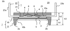
図1は、本発明の実施の形態1によるパワーモジュールの断面図である。図2は図1のパワーモジュールを金属ベース側から見た斜視図であり、図3は図1のパワーモジュールを金属ベース側から見た底面図である。図4は図1のパワーモジュールのリブ部の拡大図である。図5は、比較例のパワーモジュールの絶縁距離を説明する図であり、図4に対応する部分の拡大図である。図1は、図2の破線で示した切断面をA方向から見た断面図であり、図2と上下が逆転している。なお図3において、リードフレーム1の端子部22は省略した。パワーモジュール20は、リードフレーム1、金属ベース3、パワー素子4、絶縁シート5、樹脂筐体7を備える。パワー素子4は、入力交流電力を直流電力に変換するコンバータ部に用いるダイオードや、直流電力を交流電力に変換するインバータ部に用いるバイポーラトランジスタ、IGBT(Insulated Gate Bipolar Transistor)、MOSFET(Metal Oxide Semiconductor Field Effect Transistor)、GTO(Gate Turn-Off thyristor)等がある。
FIG. 1 is a cross-sectional view of a power module according to
絶縁シート5は、放熱性の高い絶縁層であり、リードフレーム1の配線部21と金属ベース3とを絶縁すると共に、パワー素子4が発生させた熱を金属ベース3に放熱する。絶縁シート5は、エポキシなどの熱硬化性樹脂が用いられ、その内部にはシリカや窒化ホウ素(BN(boron nitride))などの高伝導性フィラーが混入されている。金属ベース3は、パワー素子4からの熱を放熱する。金属ベース3は、銅板、アルミ板、銅箔など高熱伝導部材が用いられている。リードフレーム1は、銅板やアルミ板からプレス成形することによりパターン形成される。
The insulating
リードフレーム1は、配線部21と端子部22を備える。配線部21には、パワー素子4が搭載され、パワー素子4の裏面電極が半田等で接続される。また、複数のパワー素子4間の接続、及びパワー素子4の表面電極と配線部21との接続はワイヤ6により接続される。リードフレーム1は、パワー素子4の電極に電気的に接続される。端子部22は、外部の機器等に接続する複数の端子23a、23b、23cを有する。端子部22の各端子は、L形状に曲げられて、樹脂筐体7の本体部10より露出されている。図2では、5つの端子23a、5つの端子23b、5つの端子23cが、パワーモジュール20の3方向から出ている例を示した。パワーモジュール20の中央部には、パワーモジュール20を後述するヒートシンク16(図10参照)にねじを用いて固定する孔18が、樹脂筐体7の上面10aから金属ベース3を貫通するように設けられている。端子の符号は、総括的に23を用い、区別して説明する場合に23a、23b、23c、23d(図8参照)を用いる。
The
樹脂筐体7は、エポキシなどの熱硬化性樹脂により形成され、高温で成形して製品となり、樹脂筐体7の内部に配置した部材間の絶縁性を確保する。樹脂内部にはシリカやアルミナ、窒化ホウ素などの高伝導性フィラーが混入されている。樹脂封止はインジェクションモールド、トランスファーモールドがある。パワーモジュールではトランスファーモールドが一般的に使われる。樹脂筐体7は、金属ベース3の一面(露出面)及びリードフレーム1の一部(端子部22)が露出するようにパワー素子4を封止している。樹脂筐体7は、本体部10とリブ部11を備える。本体部10は、パワー素子4及びリードフレーム1の一部(端子部22)が内部に配置されると共に、底面10bにおいて金属ベース3の一面(露出面)が露出している。金属ベース3を露出させることで吸湿性がある樹脂の表面積を低下させることができ、吸湿によるイオンマイグレーションなどの電気的不具合を抑制する。リブ部11は、本体部10の底面10bにおいて、金属ベース3の外周を包囲するように設置されると共に、本体部10の底面10bから当該底面10bに垂直な方向に突出して設けられている。リブ部11は、本体部10の底面10bの外周に4つのリブ2a、2b、2c、2dを備える。リブの符号は、総括的に2を用い、区別して説明する場合に2a、2b、2c、2dを用いる。
The
リブ2は、樹脂筐体7の底面10bにおいて金属ベース3の側面よりも外側に設置され、金属ベース3の底面(露出面)を基準面としてリードフレーム1の端子23の曲げ方向とは反対側に突出して設けられる。また、図1に示したリブ2の断面は、本体部10の側面に平行な方向である延伸方向に垂直な方向の短手方向の断面である。このリブ2の短手方向の断面は、先端に向かうに従って小さくなるテーパ形状であり、樹脂筐体7を成形する際に使用される金型の離型性を向上させている。さらに、リブ2は金属ベース3の底面(露出面)を取り囲むように(包囲するように)同一高さで配置され、隣接するリブ間は繋がった状態である。リブ部11は、隣接するリブ間をつなげることで角部の剛性を向上させ、パワーモジュール20の対極方向(対向する3つの角方向)の曲げ剛性を向上させている。なお、樹脂筐体7を成形する際に使用する金型の離型性を向上させるため、リブ2の角にR形状及びテーパ形状を施されるのが望ましい。
The
図15、図16に示す他のパワーモジュールでは、リブ2の頂上に丸形状の窪み101を有している例を示した。図15は本発明の実施の形態1による他のパワーモジュールの断面図であり、図16は図15のパワーモジュールを金属ベース側から見た斜視図である。この窪み101は、リードフレーム1の端子23と金属ベース3間に配置され、リードフレーム1の端子23と金属ベース3間の絶縁距離を大きくする。すなわち、窪み分の絶縁距離を増やすことで、リブ2の幅を小さくすることができる。これにより、モジュール面積をさらに小型化できる。ここでは、窪み101は丸形状の例を示したが、三角形、四角形、五角形、六角形、八角形などの多角形であってもよい。
In the other power modules shown in FIG. 15 and FIG. 16, an example is shown in which the
パワー素子4は、リードフレーム1の配線部21に実装されている。リードフレーム1における、パワー素子4が実装された面と反対側の面に、絶縁シート5と金属ベース3が配置されている。パワー素子4、リードフレーム1、ワイヤ6、絶縁シート5、金属ベース3は、リードフレーム1の端子部22と金属ベース3の底面を露出した状態で樹脂筐体7により覆われる。パワー素子4の発熱はリードフレーム1、絶縁シート5、金属ベース3へと放出される。
The
実施の形態1のパワーモジュール20は、樹脂筐体7を形成する際に、半硬化の絶縁シート5が塗られた金属ベース3である銅箔の上にリードフレーム1を設置する。このとき、樹脂筐体7を形成する金型に対する銅箔の位置決めは、可動ピンを銅箔角部の縦方向と横方向に1本ずつ配置し、これらの可動ピンを銅箔の4つ角に設置することで実施している。これにより、樹脂が注入されたときの樹脂圧力で銅箔の位置ずれを抑制する。銅箔は薄いと撓みやすくなり、装置内の搬送が難しく、一方、厚いとコストが高くなることから、銅箔の厚さは0.03mmから0.1mmが望ましい。パワーモジュール20における樹脂筐体7の底面10bから露出した銅箔である金属ベース3と樹脂筐体7の底面10bとは同一面となっている。樹脂筐体7の形成工程では、金型内の樹脂充填圧と樹脂温度により、樹脂筐体7の樹脂硬化を行うと同時に、リードフレーム1を介して絶縁シート5を銅箔(金属ベース3)に押しつけながら半硬化から硬化させている。これにより絶縁シート5の高い放熱性と絶縁性を確保している。また、銅箔の厚さが0.03mmから0.1mmであれば、パワーモジュールが反り変形しやすくなり、図15に示すようにパワーモジュール20が凸形状となる。また、実施の形態1のパワーモジュール20は、モジュールの銅箔面から吸湿しないため、吸湿によるイオンマイグレーションなどの電気的不具合を抑制する。
In the
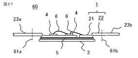
パワーモジュール20の樹脂充填に着眼すると、パワーモジュール20の樹脂筐体7の形成工程は、樹脂厚の厚いリードフレーム1の上方から粘度(粘性)の高い樹脂が充填され、流動抵抗の高いリブ2は最後に充填される。具体的には、図1のようにリブ部11が下を向くように、パワー素子4が実装されたリードフレーム1に絶縁シート5、金属ベース3が設置された中間製造部品60を、金型62に配置し(図18参照)、リードフレーム1の樹脂面(本体部10の側面)から樹脂を注入する。このとき、金型62に載せる順序は絶縁シート5、金属ベース3を先に設置し、次にパワー素子4が実装されたリードフレーム1を設置している。これにより、金属ベース3を位置決めした後、リードフレーム1の位置決めを個別にすることで、各部材の位置決め精度を向上させている。図17は、本発明の実施の形態1による中間製造部品を示す図である。図18は本発明の実施の形態1によるパワーモジュールの製造方法を説明する図であり、図19は本発明の実施の形態1による金型の断面図である。金型62は、リードフレーム1の端子部22を外部に露出させる端子開口65a、65bが設けされた金型本体63と、金型蓋64を備える。金型本体63における破線73よりも下側部分はパワーモジュール20におけるリブ部11のリブ2の端部を形成するリブ端部形成部69である。
Focusing on the resin filling of the
図19に示した、リブ高さhm1、本体部高さhm2、樹脂筐体高さhm3、本体上面側高さhm8、本体リブ側高さhm9は、それぞれ図15に示したパワーモジュール20における、リブ高さh1、本体部高さh2、樹脂筐体高さh3、樹脂厚さh8、樹脂厚さh9に相当する高さであり、樹脂筐体7の硬化に伴う縮小を考慮したサイズに設定されている。中間製造部品60を金型62に配置する際に、中間製造部品60を、金属ベース3を金属ベース配置部66に接触させると共にリードフレーム1の一部が金型62から露出するように、金型62に配置する。図17に示した破線61aから左側の部分と、破線61bから右側の部分は、樹脂筐体7から露出する部分である。金属ベース3を金属ベース配置部66に接触させて中間製造部品60を金型62に配置することで、金属ベース3の一面が露出したパワーモジュール20を製造することができる。なお、樹脂筐体7から露出した端子部22は、樹脂筐体7を形成する樹脂筐体形成工程の後に、L形状に曲げられて、複数の端子23a、23bを完成品(製品のパワーモジュール)の向きに形成する。
The rib height hm1, the main body height hm2, the resin housing height hm3, the main body upper surface side height hm8, and the main body rib side height hm9 shown in FIG. 19 are ribs in the
図20は本発明の実施の形態1による他の金型の断面図であり、図21は図20の金型本体及び金型蓋の断面図である。図15に示したパワーモジュール20における樹脂筐体7の形成工程では、図20に示した金型62を用いる。図20に示した金型62は、端子開口65a、65b及びピン開口67a、67bを有する金型本体63と、金型蓋64と、ピン開口67a、67bに移動可能に挿入された、離型性を向上させる突き出しピン71を備える。突き出しピン71はバネ(図示せず)により動作する。金型62が締まった状態、すなわち閉じた状態では突き出しピン71は動作せず、金型62が開くと同時にバネにより突き出しピン71が動作する。ピン開口67aは図15のパワーモジュール20のリブ2aを押出す際に、ピンを挿入する貫通孔である。同様に、ピン開口67bは図15のパワーモジュール20のリブ2bを押出す際に、ピンを挿入する貫通孔である。図20に示した金型62を用いて、樹脂筐体7を形成する工程である樹脂筐体形成工程を実行する際は、ピン開口67a、67bに突き出しピン71でピン開口67a、67bを閉じる。ピン開口67a、67bが閉じられた状態で、樹脂筐体形成工程が実行され、樹脂筐体7を形成する樹脂(トランスファーモールド樹脂)が樹脂硬化した後に、金型62が開いたと同時にピン開口67a、67bから突き出しピン71が樹脂筐体7側に出て樹脂筐体7のリブ部11を押出して、樹脂筐体7を金型62から取り出す(樹脂筐体取出工程)。この金型62から樹脂筐体7を取り出す際に、リブ部11に窪み101が形成される。このため、樹脂筐体取出工程は、リブ部11に窪み101を形成する工程(リブ部窪み形成工程)でもある。リブ部11の窪み101の深さはリブ部11の底面、すなわち本体部10から突出したリブ2の最遠方の端部の幅ws1(図3参照)より大きくしており、樹脂を金型内に入り込んで付着しないようにして、金型62の清掃をしやすくしている。
FIG. 20 is a cross-sectional view of another mold according to
なお、樹脂筐体7を形成する金型に彫り込みを入れて、この掘り込みに銅箔を設置しても良い。この掘り込みにより、樹脂筐体7を形成する金型に対する銅箔である金属ベース3の位置決めを行うことができる。この場合、銅箔面はパワーモジュール20における樹脂筐体7の底面10bよりも出っ張ることになるが、この形状でも構わない。
In addition, you may insert in a mold which forms the
一方、従来のパワーモジュールは本体部しかないので、樹脂筐体を形成する樹脂筐体形成工程において、以下のような問題が懸念されていた。樹脂筐体形成工程において、リードフレーム1に実装されたパワー素子4が上を向くように金型に配置された場合には、本体部の側面側から樹脂を注入するので、リードフレーム1のパワー素子実装面側又は側面にエアが残り、空隙となることが懸念された。特に空隙の周辺にワイヤ6があると、ワイヤ6の被覆している樹脂筐体7が薄くなる問題、又はワイヤ6が樹脂筐体7の外部へ露出する問題が懸念された。このような状態になると、ワイヤ6とパワーモジュール20の外側に配置された部品間で空間絶縁距離が小さくなり、絶縁性を確保できなくなることが懸念された。
On the other hand, since the conventional power module has only the main body, the following problems have been concerned in the resin case forming step of forming the resin case. In the resin housing formation step, when the
実施の形態1のパワーモジュール20は、樹脂筐体形成工程において、パワーモジュール20のリブ2が樹脂充填の最後となるため、リードフレーム1のパワー素子実装面側又は側面にエアが残って空隙とならない。その結果、ワイヤ露出など発生せずにパワーモジュール20の外側に配置された部品との空間絶縁距離を確保することができる。
In the
また、実施の形態1のパワーモジュール20は、リブ部11の各リブ2a、2b、2c、2dの高さであるリブ高さh1が、リードフレーム1を封止する本体部10の高さである本体部高さh2よりも小さくしている。すなわち、h1<h2の関係になっている。樹脂筐体高さh3は、リブ高さh1と本体部高さh2との合計なので、h1<0.5×h3の関係も成立している。
Further, in the
パワーモジュール20を製作する上で、樹脂筐体7の樹脂の硬化時間と同時に絶縁シート5の硬化させる時間を合わせる必要がある。樹脂筐体7の樹脂の硬化時間が長くなると、絶縁シート5が先に硬化するため、リードフレーム1と絶縁シート5との密着が悪くなり、放熱性や絶縁性を確保できなくなる。そのため、パワーモジュール20のリブ高さh1は本体部高さh2よりも小さくし、リブ部11の樹脂充填量を減らし、リブ部11の樹脂充填時間を短縮している。リブ部11のリブ構造は、前述したようにリブ2の断面がテーパ形状であり、すなわち樹脂充填性を上げるためにリブ2にテーパを設けている。リブ部11のリブ2と本体部10とが接続された接続部の幅(接続幅)はリブ根元幅wb1であり、本体部10から突出したリブ2の最遠方の端部の幅は端部幅ws1である。リブ部11のリブ2はテーパが設けられているので、端部幅ws1はリブ根元幅wb1より小さくなっており、すなわちws1<wb1の関係が成立している。
When manufacturing the
金型62内ではパワーモジュール20のリブ部11を形成する溝が細いため、金型62からパワーモジュール20を取り出すときに、金型62に樹脂が残ること、すなわちリブ部の形状崩れが懸念される場合がある。しかし、リブ部の形状崩れが懸念される場合には、図20の金型62を用いて樹脂筐体7を形成し、リブ側からピンで押して、パワーモジュール20を金型から押し出すことで、離型性を改善することができる。このとき、パワーモジュール20のリブ2に窪み101が形成される。この窪み101を残すことで、リードフレーム1の端子23と金属ベース3間の絶縁距離を大きくすることができる。ピンは、離型性の観点から断面は円形状が好ましい。そのため、製造方法と絶縁距離確保の観点を両立できるため、窪み101の形状は丸形状が好ましい。
Since the groove for forming the
実施の形態1のパワーモジュール20は、樹脂筐体7の樹脂の充填時間内で絶縁シート5を硬化させることができ、絶縁シート5の放熱性と絶縁性を確保できる。
The
実施の形態1のパワーモジュール20は、リブ部11のリブ2が、リードフレーム1と金属ベース3との間の沿面距離である下外周部長Liを長くすることができる。リードフレーム1と金属ベース3との間の沿面距離である下外周部長Liはリードフレーム1と金属ベース3との間の絶縁距離(沿面距離)に相当するので、実施の形態1のパワーモジュール20は、リードフレーム1と金属ベース3との間の絶縁距離(沿面距離)を長くすることができる。図4及び図5を用いて、実施の形態1のパワーモジュール20の下外周部長Liを説明する。なお、図5の比較例のパワーモジュール100において、実施の形態1のパワーモジュール20のリブ2を破線で示した。
In the
実施の形態1のパワーモジュール20におけるリードフレーム1と金属ベース3との間の沿面距離である下外周部長Liは、金属ベース3の外周からリブ部11のリブ2までの長さである樹脂底面長L1、リブ2の外周の長さである外周長L2、本体部10におけるリブ部11との境界からリードフレーム1の端子部22までの長さである本体底部長L3の合計長さである。リブ2を有しないパワーモジュール(比較例)のリードフレーム1と金属ベース3との間の絶縁距離(沿面距離)Lexを、実施の形態1のパワーモジュール20で説明した長さ及び幅を使って説明する。比較例のパワーモジュール100におけるリードフレーム1と金属ベース3との間の絶縁距離(沿面距離)Lexは、樹脂底面長L1、リブ根元幅wb1、本体底部長L3の合計長さである。リブ2のリブ根元幅wb1はリブ2の外周長L2よりも短いので、実施の形態1のパワーモジュール20の絶縁距離(下外周部長Li)は比較例のパワーモジュールの絶縁距離Lexよりも長くすることができる。また、実施の形態1のパワーモジュール20は、リブ2のリブ高さh1が高いほどリブ2の外周の長さである外周長L2を長くすることができる。
The lower outer peripheral length Li, which is a creeping distance between the
実施の形態1のパワーモジュール20における下外周部長Liを比較例のパワーモジュール100の絶縁距離Lexと等しくすることを考える。この場合、実施の形態1のパワーモジュール20は、リードフレーム1が露出する樹脂筐体7における本体部10の側面(端部)と金属ベース3の外周(端部)との端部間長L4(図3参照)を比較例のパワーモジュール100よりも短くできる。端部間長L4は、樹脂底面長L1とリブ2のリブ根元幅wb1との合計長さである。したがって、実施の形態1のパワーモジュール20は、絶縁距離の等しい比較例のパワーモジュール100よりもパワーモジュールの面積が小さくでき、小型化できる。
The lower outer peripheral length Li in the
また、パワーモジュール20のリブ高さh1がリブ根元幅wb1より大きなっており、絶縁距離をリブ高さ方向に伸ばすことにより、パワーモジュール20の面積をさらに小さくできる。また、図15に示すようにパワーモジュール20のリードフレーム1における樹脂筐体7から突出する下端面から上側の樹脂厚さh8からリードフレーム1の厚さを引いた厚さである樹脂厚さh10が、リードフレーム1の下端面から下側の樹脂厚さh9より大きい場合には、下端面から下側の樹脂が熱収縮しやすい。特に、樹脂筐体7がリードフレーム1よりも線膨張が小さいと顕著になる。樹脂厚さh10は、リードフレーム1が樹脂筐体7から突出するフレーム接触部51の上面10a側であるフレーム接触部上面51aと上面10aとの最大の厚さである。樹脂厚さh9は、フレーム接触部51の底面10b側であるフレーム接触部底面51bと金属ベース3の露出面との最小の厚さである。フレーム接触部51の形状は、樹脂筐体7から突出するリードフレーム1の断面形状と同じである。さらに、パワーモジュール20の端部のリブ2を含めると、樹脂量が大きくなり、下端面から下側の熱収縮することで、パワーモジュール20の金属ベース3の露出面を上下方向の基準として上方向に凸形状に反りやすくなる。樹脂厚さh8からリードフレーム1の厚さを引いた厚さである樹脂厚さh10を樹脂厚さh9より大きくするには、本体上面側高さhm8が本体リブ側高さhm9より大きい金型62を用いることで、樹脂筐体形成工程を実行することで実現できる。
The rib height h1 of the
さらに、実施の形態1のパワーモジュール20は、リブ2が梁の役割を兼ねることでパワーモジュールの曲げ剛性が向上する。実施の形態1のパワーモジュール20は、パワーモジュールの曲げ剛性が向上するので、高温で樹脂筐体7が成形されたパワーモジュールが常温まで冷却されることで発生する樹脂の熱収縮や、この冷却過程でリードフレーム1、金属ベース3、樹脂筐体7などの部材の線膨張差の違いによるパワーモジュールの反り量を低減することができる。その結果、実施の形態1のパワーモジュール20は、特許文献1のような押さえ部材を使用する必要がなく、パワーモジュールをヒートシンクに固定する工程を特許文献1のパワーモジュールよりも短くするこができる。また、実施の形態1のパワーモジュール20は、特許文献1のような押さえ部材を使用する必要がないので、押さえ部材の費用が発生しないので、低コスト化できる。
Furthermore, in the
実施の形態1のパワーモジュール20は、樹脂筐体7の本体部10の底面10bにおいて、金属ベース3の外周を包囲するように設置されると共に、本体部10の底面10bから当該底面10bに垂直な方向に突出して設けられたリブ部11を備えており、すなわち樹脂筐体7の底面10bにおいて金属ベース3の側面よりも外側に設置されると共に底面10bから突出して設けられたリブ2を備えるので、リードフレーム1と金属ベース3との間の絶縁性を高めながら小型にできる。また、実施の形態1のパワーモジュール20は、本体部10の底面10bよりも内側に絶縁シート5が配置されているので、高価な絶縁シート5を最小サイズにしている。
なお、図1では、リードフレーム1は絶縁シート5と接触する端面より内側に段差を設けて配線部21を配置した例を示した。この配線部21と端子部22との段差により、端子部22は配線部21よりも金属ベース3からの高さが高くなるので、この段差に相当する樹脂筐体7の厚さ分によりリードフレーム1と金属ベース3との絶縁距離を長くしている。本実施の形態では、例えばリードフレーム1の厚さ0.6mmに対して、段差量は0.3mmとリードフレーム1の厚さに対して半分以下になるように形成している。これは、リードフレーム1の段差加工がプレス工程等で製作される場合、リードフレーム1の段差量が多いと破断等の懸念があるため、破断しない段差にする必要がある。リードフレーム1の厚さが大きいと、リードフレーム材と樹脂との線膨張差により、パワーモジュール20の反り量が大きくなるため、リードフレーム1の厚さは0.3〜1.0mmの範囲が望ましい。
Note that FIG. 1 shows an example in which the
実施の形態1のパワーモジュール20は、リードフレーム1の段差加工を行うことで、リードフレーム1を薄い状態で樹脂封止でき、モジュール厚さを薄く、かつ均一化できる。モジュール厚さを薄くする場合には、パワーモジュール20のモジュール厚さ、すなわち本体部高さh2は5mm〜15mmの範囲が望ましい。また、パワーモジュール20の凸形状の反り量が0.1mmを超えると、ねじ締め力でパワーモジュール20を平坦にするのが難しいため、反り量は0.1mm以下にすることが望ましい。また、実施の形態1のパワーモジュール20は、リブ高さh1をリブ根元幅wb1より大きくすることで、モジュールの絶縁性の確保と小型化を両立している。
In the
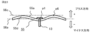
ここで、パワーモジュールの反り量を説明する。図22は、パワーモジュールの反り量を説明する図である。図23はパワーモジュールのプラス方向の反り量を説明する図であり、図24はパワーモジュールのマイナス方向の反り量を説明する図である。図22〜図24では、パワーモジュール55がねじ止めされる前の状態を示している。図22〜図24のパワーモジュール55はリブ部11や金属ベース3等が省略され簡略化している。図22の上側にパワーモジュール55の側面であるパワーモジュール側面55cを示し、下側にパワーモジュール55の上面であるパワーモジュール上面55aを示した。パワーモジュール55の底面であるパワーモジュール底面55bには、図示しない金属ベース3が配置されている。このパワーモジュールの反り量は、本願のパワーモジュール20にも適用できる。
Here, the amount of warpage of the power module will be described. FIG. 22 is a diagram for explaining the amount of warpage of the power module. FIG. 23 is a view for explaining the amount of warpage in the positive direction of the power module, and FIG. 24 is a view for explaining the amount of warpage in the negative direction of the power module. FIG. 22 to FIG. 24 show the state before the
パワーモジュール55の反り量の方向を示す「+」(「プラス」)、「−」(「マイナス」)は金属ベース3の露出面(図22のパワーモジュール底面55b)を上下方向の基準とし、「+」は反りが上方向に凸形状、「−」は反りが下方向に凸形状とする。ただし、反り量はパワーモジュール55の上面(パワーモジュール上面55a)で測定する。そこで、図22〜24では、実際に測定するパワーモジュール上面55aの破線56aを基準にしている。パワーモジュール55がねじ止めされる前では、図22に示しように、パワーモジュール55の樹脂側、すなわちパワーモジュール上面55aの中心の計測点p1と、4隅の計測点p2、p3、p4、p5の平均との差で表記する。図22では、計測点p1が上方向の最も高い位置にあり、4隅の計測点p2、p3、p4、p5が計測点p1よりも低い位置にある。破線56bは、反り量の絶対値が最大となる計測点を通り、破線56aに平行である。なお、基準となる破線56aは、例えば、ねじ止めするねじ13が貫通する孔18に垂直に設定する。したがって、図22のパワーモジュール55は、反り量が「−」であり、反りが下方向に凸形状である。
“+” (“Plus”) and “−” (“minus”) indicating the direction of the amount of warpage of the
図23、図24では、パワーモジュール上面55aの中心の計測点p1においてねじ13で図示しないヒートシンク16にねじ止めする状態を示している。図23、図24では、パワーモジュール55の断面であるパワーモジュール断面55dを示している。なお、断面を示す斜線は省略している。ねじ止めしている状態のパワーモジュール55の反り量は、中心の計測点p1、すなわち破線56aを基準にして、中心の計測点p1から高さ方向に最も離れた点である計測点と計測点p1との差を反り量とする。図23のパワーモジュール55では、中心の計測点p1から高さ方向に最も離れた点である計測点p6と計測点p1との差を反り量とする。破線56cは計測点p6を通り、破線56aに平行である。図23のパワーモジュール55は、反り量が「+」であり、反りが上方向に凸形状である。図24では、パワーモジュール55では、中心の計測点p1から高さ方向に最も離れた点である計測点p7と計測点p1との差を反り量とする。破線56dは計測点p7を通り、破線56aに平行である。図24のパワーモジュール55は、反り量が「−」であり、反りが下方向に凸形状である。なお、図24のパワーモジュール55は、図22のパワーモジュール55のねじ止めの初期状態を示しており、図23のパワーモジュール55は、図22のパワーモジュール55のねじ止めの最終状態を示している。
FIG. 23 and FIG. 24 show a state in which the
また、本実施の形態では、絶縁シート5と金属ベース3を個別で組み合わせて一体化したものを用いているが、これに限らず一般的なセラミック基板や金属基板を備えたパワーモジュールにも本実施の形態のリブ構造を適用できる。また、絶縁シート5を用いずに、パワー素子4が厚い金属ベース3に接続されたものでも、本実施の形態のリブ構造を適用できる。
Further, in the present embodiment, although the insulating
以上のように、実施の形態1のパワーモジュール20は、パワー素子4と、パワー素子4からの熱を放熱する金属ベース3と、パワー素子4の電極に電気的に接続されたリードフレーム1と、金属ベース3の一面及びリードフレーム1の一部が露出するようにパワー素子4を封止する樹脂筐体7とを備える。パワーモジュール20の樹脂筐体7は、パワー素子4及びリードフレーム1の一部が内部に配置されると共に、底面10bにおいて金属ベース3の一面が露出した本体部10と、本体部10の底面10bにおいて、金属ベース3の外周を包囲するように設置されると共に、本体部10の底面から当該底面10bに垂直な方向に突出して設けられたリブ部11を備えたことを特徴とする。実施の形態1のパワーモジュール20は、樹脂筐体7の本体部10の底面10bにおいて、金属ベース3の外周を包囲するように設置されると共に、本体部10の底面10bから当該底面10bに垂直な方向に突出して設けられたリブ部11を備えたので、リードフレーム1と金属ベース3との間の絶縁性を高めながら小型にできる。さらに、実施の形態1のパワーモジュール20は、リブ2の梁効果により、パワーモジュール20の剛性を上げて、反り量を効果的に制御できる。
As described above, the
実施の形態1のパワーモジュール20を製造するパワーモジュール製造方法は、パワー素子4と、金属ベース3と、リードフレーム1を備えた中間製造部品60を、金属ベース3が金属ベース配置部66に接触すると共にリードフレーム1の一部が金型62から露出するように、金型62に配置する工程と、金型62にトランスファーモールド樹脂を注入し、樹脂筐体7を形成する工程と、を含むことを特徴とする。実施の形態1のパワーモジュール製造方法は、樹脂筐体7の本体部10の底面10bにおいて、金属ベース3の外周を包囲するように設置されると共に、本体部10の底面10bから当該底面10bに垂直な方向に突出して設けられたリブ部11を備えたパワーモジュール20を製造するこができる。また、実施の形態1のパワーモジュール製造方法は、金属ベース3が接触する金属ベース配置部66とリードフレーム1が露出する開口(端子開口65a、65b)における金属ベース側の開口端との、樹脂筐体7の底面10bに垂直な方向の長さ(本体リブ側高さhm9)が、パワーモジュール20の底面10bと反対側の上面10aが形成される内面と前記開口端との、樹脂筐体7の底面10bに垂直な方向の長さ(本体上面側高さhm8)よりも短くした金型62を用いることで、露出した金属ベース3の一面を上下方向の基準として、上方向に凸形状であるパワーモジュール20を製造することができる。
The power module manufacturing method for manufacturing the
また、実施の形態1のパワーモジュール製造方法は、樹脂筐体7における底面10bから突出したリブ部11の端部が形成されるリブ端部形成部69に、樹脂筐体7を押出すピンを挿入するピン開口67a、67bが複数形成されている金型62を用い、ピン開口67a、67bが閉じられた状態で、樹脂筐体7を形成する工程が実行され、樹脂筐体7を金型62から取り出す際に、ピン開口67a、67bからピンを挿入して樹脂筐体7のリブ部11を押出して、リブ部11に窪み101を形成する工程を含むことを特徴とする。実施の形態1のパワーモジュール製造方法は、ピン開口67a、67bが複数形成されている金型62を用いることで、底面10bから突出した端部に窪み101を有するリブ部11を備えたパワーモジュール20を製造することができる。
Further, in the power module manufacturing method according to the first embodiment, a pin for pushing the
実施の形態2.
図6は、本発明の実施の形態2によるパワーモジュールの断面図である。実施の形態2のパワーモジュール20は、リブ部11のリブ2の形状が実施の形態1と異なる。リブ2は、リブ土台部26と凸部27を備えている。実施の形態2のパワーモジュール20は、実施の形態1と同様に、樹脂筐体7の底面10bにおいて金属ベース3の側面よりも外側に設置されると共に底面10bから突出して設けられたリブ2を備えるので、リードフレーム1と金属ベース3との間の絶縁性を高めながら小型にできる。図6では、リブ2a、2bを記載した。凸部27はリブ土台部26の上に小さいリブを配置した形状している。リブ土台部26は本体部10の底面10bに接続されており、凸部27はリブ土台部26における本体部10の底面10bから突出した端部に設置されると共に本体部10の底面10bに垂直な方向に突出して設けられている。凸部27の小さいリブ形状は先端が細くなるので、先端部をR形状するなど、衝撃で欠けない対策をするのが望ましい。Second Embodiment
FIG. 6 is a cross-sectional view of a power module according to
図6に示したリブ2の断面は、図1と同様に、本体部10の側面に平行な方向である延伸方向に垂直な方向の短手方向の断面である。リブ土台部26は、短手方向の断面であって本体部10の底面10bに垂直な断面の形状が、本体部10の底面10bに接続した接続幅が底面10bから突出した端部であるリブ土台部端部の幅よりも大きいテーパ形状であり、凸部27は、短手方向の断面であって本体部10の底面10bに垂直な断面の形状が、リブ土台部26に接続した接続幅がリブ土台部端部から突出した端部である凸部端部の幅よりも大きいテーパ形状である。
The cross section of the
実施の形態2のリブ2は、2段形状になっており、凸部27のテーパ傾斜がリブ土台部26のテーパ傾斜よりも急になっているので、実施の形態1のような1段形状のリブと比べて、同じ高さであってもリブ2の外周長L2が長くなる。したがって、実施の形態2のパワーモジュール20は、同じ高さのリブ2で1段形状のものと比べてリードフレーム1と金属ベース3との間の下外周部長Liを大きくすることができ、すなわちリードフレーム1と金属ベース3との間の絶縁距離を大きくすることができる。さらに、実施の形態2のパワーモジュール20は、必要な絶縁距離を形成する場合に、実施の形態1のパワーモジュール20よりもリブ高さh4を小さくできる。
The
実施の形態2のパワーモジュール20は、樹脂筐体7における本体部10の高さが本体部高さh2であり、リブ部11の高さがリブ高さh4であり、樹脂筐体7の高さが樹脂筐体高さh5である。リブ高さh4は実施の形態1のリブ高さh1よりも小さいので、実施の形態2のパワーモジュール20は、リードフレーム1と金属ベース3との間の絶縁距離を十分確保しながら、樹脂筐体7の高さを小さくでき、実施の形態1のパワーモジュール20よりも樹脂筐体7が小型にできる。さらに、実施の形態2のパワーモジュール20は、リブ2の樹脂量を減らすことができ、樹脂筐体7の樹脂コストを低減することができる。
In the
実施の形態3.
図7は、本発明の実施の形態3によるパワーモジュールの断面図である。実施の形態3のパワーモジュール20は、リブ部11におけるリブ2の高さを2種類にした点で、実施の形態1と異なる。図7では、リブ2aの高さがリブ高さh1であり、リブ2bの高さがリブ高さh6の例を示した。Third Embodiment
FIG. 7 is a cross-sectional view of a power module according to a third embodiment of the present invention. The
リードフレーム1と金属ベース3との絶縁距離は、各端子23に必要な電圧で決まる。例えば、IGBT、FwD(Free Wheeling Diode)、CVD(Converter Diode)などのパワー素子4が実装されているリードフレーム1の出力端子である端子23aは高電圧である。一方、IGBTのゲートを制御するリードフレーム1の制御端子、あるいは電流センサ用の電流を検出するリードフレーム1の制御端子である端子23bは低電圧である。図7に示したリブ2a、2bは、それぞれ高電圧側リブ、低電圧側リブと呼ぶこともできる。
The insulation distance between the
そこで、高電圧となるリードフレーム1の出力端子である端子23aと金属ベース3との間のリブ2aの高さは高くし、低電圧となるリードフレーム1の制御端子である端子23bと金属ベース3との間のリブ2bの高さを低くすることができる。すなわち、高電圧側リブ2aの高さは高くし、低電圧側リブ2bの高さを低くすることができる。本実施の形態では、図2に示したパワーモジュール20と同様に、3方向からリードフレーム1の端子23が出ており、リードフレーム1の端子が出ない方向、すなわちリブ2dは、低電圧であるため、高さがリブ高さh6の低電圧側リブが使用される。リブ2cについては、端子23cが高電圧となる端子であれば高電圧側リブを用い、端子23cが低電圧となる端子であれば低電圧側リブを用いる。
Therefore, the height of the
実施の形態3のパワーモジュール20は、実施の形態1と同様に、樹脂筐体7の底面10bにおいて金属ベース3の側面よりも外側に設置されると共に底面10bから突出して設けられたリブ2を備えるので、リードフレーム1と金属ベース3との間の絶縁性を高めながら小型にできる。実施の形態3のパワーモジュール20は、リブ部11の複数のリブ2のうち、少なくとも1つのリブ(リブ2b、2d)は、本体部10の底面10bと当該リブ(リブ2b、2d)の本体部10の底面10bから最も遠方の端部との高さであるリブ高さh6が、他のリブ(リブ2a)におけるリブ高さh1よりも低くなっている。実施の形態3のパワーモジュール20は、リードフレーム1の端子の電圧に応じて、高さの異なるリブ2を備えるので、パワーモジュールの反り低減効果を保ちつつ、樹脂筐体7の樹脂量を少なくして、樹脂筐体7の樹脂コストを低減できる。なお、リブ部11におけるリブ2の高さを2種類にした例で説明したが、3種類以上であっても構わない。
As in the first embodiment, the
実施の形態4.
図8は本発明の実施の形態4によるパワーモジュールの斜視図であり、図9は図8のパワーモジュールを金属ベース側から見た底面図である。なお図9において、リードフレーム1の端子部22は省略した。実施の形態4のパワーモジュール20は、樹脂筐体7の上面10a又は底面10bから見た外形が長方形である点で、実施の形態1と異なる。なお、樹脂筐体7の上面10a又は底面10bから見た外形が長方形に限らず、長辺及び短辺を有する四辺形状であっても構わない。パワーモジュール20の外観はリードフレーム1の端子23が4方向から端子が出ている形状であり、パワーモジュール20を固定する孔18が2ヶ所設けられている。パワーモジュール20の長辺の外周側において長手方向に配置されたリブ2c、2dは、短辺の外周側において短手方向に配置されたリブ2a、2bに比べて厚さが大きい。また、本実施の形態ではパワーモジュール20の側面から出るリードフレーム1の端子23を4方向としたが、端子23の突出方向の数はこれに限定されない。図8では、長辺の外周側に配置されたリブ2a、2bが設けられた樹脂筐体7の側面ではそれぞれ5本の端子23a、23bが出ており、短辺の外周側に配置されたリブ2c、2dが設けられた樹脂筐体7の側面ではそれぞれ6本の端子23c、23dが出ている例を示した。Fourth Embodiment
8 is a perspective view of a power module according to a fourth embodiment of the present invention, and FIG. 9 is a bottom view of the power module of FIG. 8 as seen from the metal base side. In FIG. 9, the
一般的に、パワーモジュールの長手方向は短手方向よりも反り量は大きい。そのため、パワーモジュールの短手方向ではパワーモジュールの反りが小さいため、リブ2を備えた実施の形態3のパワーモジュール20は、短手方向に配置されたリブ2a、2bは長手方向に配置されたリブ2c、2dよりも厚みを小さくできる。なお、適宜、短手方向に配置されたリブを短手方向のリブ、或いは短辺リブと呼び、長手方向に配置されたリブを長手方向のリブ、或いは長辺リブと呼ぶことにする。
In general, the amount of warping in the longitudinal direction of the power module is larger than that in the lateral direction. Therefore, since the warp of the power module is small in the lateral direction of the power module, in the
実施の形態4のパワーモジュール20は、実施の形態1と同様に、リブ部11のリブ構造はリブ2の断面がテーパ形状である。リブ部11の短手方向のリブ2a、2bと本体部10との接続部の幅はリブ根元幅wb1であり、本体部10から突出したリブ2a、2bの最遠方の端部の幅は端部幅ws1である。リブ部11の長手方向のリブ2c、2dと本体部10との接続部の幅はリブ根元幅wb2であり、本体部10から突出したリブ2c、2dの最遠方の端部の幅は端部幅ws2である。リブ部11のリブ2a、2b、2c、2dはテーパが設けられているので、端部幅ws1、ws2はそれぞれリブ根元幅wb1、wb2より小さくなっており、すなわちws1<wb1及びws2<wb2の関係が成立している。
In the
実施の形態4のパワーモジュール20は、短手方向のリブ2a、2bは長手方向のリブ2c、2dよりも厚みを小さくしており、すなわち短手方向のリブ根元幅wb1は長手方向のリブ根元幅wb2よりも小さく、及び短手方向の端部幅ws1は長手方向の端部幅ws2よりも小さくなっている。すなわち、wb1<wb2及びws1<ws2の関係が成立している。
In the
実施の形態4のパワーモジュール20は、実施の形態1と同様に、樹脂筐体7の底面10bにおいて金属ベース3の側面よりも外側に設置されると共に底面10bから突出して設けられたリブ2を備えるので、リードフレーム1と金属ベース3との間の絶縁性を高めながら小型にできる。また、実施の形態4のパワーモジュール20は、短手方向のリブ2a、2bは長手方向のリブ2c、2dよりも厚みが小さくなっているので、パワーモジュールの反り低減効果を保ちつつ、樹脂筐体7の樹脂量を少なくして、樹脂筐体7の樹脂コストを低減できる。
As in the first embodiment, the
実施の形態5.
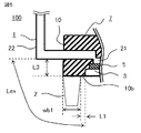
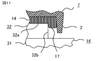
図10は本発明の実施の形態5によるパワー半導体装置の断面図である。図11は図10のパワー半導体装置の要部を示す図であり、図12は図10のパワー半導体装置の斜視図である。図10は、図12の破線で示した切断面をB方向から見た断面図である。実施の形態5では、パワーモジュール20と、ヒートシンク16を備えたパワー半導体装置40の例を説明する。パワーモジュール20の構成は、実施の形態1と同じ例で説明する。ヒートシンク16は、ヒートシンク土台部31と、ベース段差部32と、フィン33を備える。パワーモジュール20の金属ベース3の底面は、ヒートシンク16に設けられたベース段差部32の平坦な上面32aにグリース14が塗布され、ねじ13でグリース14を介してヒートシンク16に締結される。パワーモジュール20のパワー素子4から生じた発熱は金属ベース3からグリース14を介してヒートシンク16のベース段差部32へ伝わり、ヒートシンク16のヒートシンク土台部31、フィン33へ放出される。
FIG. 10 is a cross-sectional view of a power semiconductor device according to a fifth embodiment of the present invention. 11 is a view showing the main part of the power semiconductor device of FIG. 10, and FIG. 12 is a perspective view of the power semiconductor device of FIG. FIG. 10 is a cross-sectional view of the cut surface shown by the broken line in FIG. 12 as viewed from the B direction. In the fifth embodiment, an example of a
ベース段差部32の平坦な上面32aは、金属ベース3の平坦な底面よりも大きくなっている。これは、パワー素子4の発熱が金属ベース3から放出される放熱面積を、ベース段差部32で放熱面積を拡大させて、パワー素子4から生じた発熱の放熱性を向上するためである。ベース段差部32は、ヒートシンク土台部31、フィン33と一体構造であり、銅、アルミなどの高伝導部材が使用される。なお、これに限らず、ベース段差部32は別部品としてヒートシンク土台部31と接続しても構わない。
The flat
また、パワーモジュール20のリブ部11はベース段差部32の外周を覆うようにヒートシンク16に固定されるので、図11に示すように、グリース14はベース段差部32とリブ2によりグリース溜り17が発生している。実施の形態5のパワー半導体装置40は、グリース溜り17を設けることで、パワーモジュール20とヒートシンク16とをねじ締結する際に、金属ベース3とベース段差部32の合わせ面から排出されるグリース14がベース段差部32の側面32bまでまわり込む。このため、実施の形態5のパワー半導体装置40は、グリース14とベース段差部32との接触面積が増大するので、グリース14への熱伝導がよくなり、放熱性が向上する。また、実施の形態5のパワー半導体装置40は、パワーモジュール20のリブ2がヒートシンク16のヒートシンク土台部31に接しないように、ベース段差部32の高さは大きくしている。すなわち、ベース段差部32の高さがリブ2のリブ高さh1よりも大きくなっている。なお、実施の形態3のようにリブ2のリブ高さが複数ある場合は、ベース段差部32の高さが最も高いリブ高さよりも大きい。
Further, since the
また、図15に示した凸形状のパワーモジュール20を中心付近1点でヒートシンク16とねじ締めをする場合、パワーモジュール20の端部はヒートシンク16のベース段差部32の上面32aに接した状態から、パワーモジュール20の中央の隙間をねじ締め力により、パワーモジュール20はバネを締めつけるようになる。このように、凸形状のパワーモジュール20では、金属ベース3をヒートシンク16のベース段差部32の上面32aに塗布されたグリース14に押しつけながら、パワーモジュール20を凸形状から平坦形状にし、グリース14を薄く形成する。グリース14を薄くするほど、熱伝導率が大きくなるので、パワーモジュール20は放熱性が向上する。
When screwing with the
また、一般的に、パワーモジュールはグリースを介してヒートシンクにねじ固定されている。この状態でパワーモジュールを冷熱環境下で連続して使用すると、パワーモジュールの部材間で線膨張差による膨張と収縮が繰り返すため、パワーモジュールは平坦な状態から反りのある状態、及び反りのある状態から平坦な状態のようになり、モジュール端辺で反りと平坦の動作を繰り返す。そのため、グリースがパワーモジュール端辺から外へ排出させるポンピングアウト現象が発生し、放熱性が阻害されることが知られている。しかしながら、凸形状のパワーモジュール20を搭載した、実施の形態5のパワー半導体装置40では、パワーモジュール20のバネ力を利用して、ねじ13で締めけているため、ヒートシンク16に押し付けた状態を保持して、グリース14の排出を抑制している。ねじ締め状態でのパワーモジュール20の反り量は、図15に示したようにパワーモジュール20が上に凸とした場合に、−50〜+50μmとなる。この反り量は、グリース14がパワーモジュール20の中央に残る場合や、モジュールの両端に残る場合などで決まる。また、グリース14のフィラー径に由来しており、一般的に50μm以下である。ここで、ねじ止め時の反り量は、図22〜図24の通り、ねじ止め部のモジュール最表面側を基準に、上方向を「+」(「プラス」)、下方向を「−」「マイナス」)とする。0μmは平坦を意味する。プラス方向の反りがある場合には、パワーモジュール20の形状が図23のM字のような形状、すなわち、ねじ止め部のモジュール表面(上面10a)よりも上側に高い最高部(計測点p6を含む部分)を有する形状である。また、マイナス方向の反りがある場合には、パワーモジュール20の形状が上に凸の形状となる。元々、上に凸の形状をねじ締めするからである。反り量が−50〜0μmの形状の方が、信頼性が高くより好ましい。
Also, generally, the power module is screwed to the heat sink via grease. In this state, if the power module is continuously used in a cold environment, expansion and contraction due to the difference in linear expansion are repeated between the members of the power module, so the power module is warped from a flat state and a warped state It becomes flat state, and repeats warping and flat operation at the module edge. Therefore, it is known that the pumping-out phenomenon which grease discharges from a power module end side generate | occur | produces, and heat dissipation is inhibited. However, in the
図10〜図12に示した実施の形態5のパワー半導体装置40は、パワーモジュール20のリブ部11よりも低い位置にある樹脂筐体7の底面10b及び金属ベース3の底面(適宜、モジュール内側底面と呼ぶ)に、ヒートシンク16のベース段差部32を挿入して、中央部に形成された孔18にねじ13を挿入して1点で締結する。パワーモジュール20のリブ2は、リブ2の端部がヒートシンク16のベース段差部32の上面32aより低く、ヒートシンク16のヒートシンク土台部31に接しない位置でねじ締結される。そのため、実施の形態5のパワー半導体装置40は、ベース段差部32とリブ2間にグリース溜り17が発生し、製品を設置した状態で長期間使用しても、グリース14がたれる懸念が低減される。また、パワーモジュール20のリブ2はヒートシンク16と接しない位置にあるため、実施の形態5のパワー半導体装置40は、リブ2があってもパワーモジュール20が浮かない状態でねじ締めができる。ヒートシンク16は、ベース段差部32と共に一体で製作されたものであるが、ベース段差部32が別部品として製作されても同じ効果を得る。リブ部11を有しない比較例のパワーモジュール100において、このような1点締結を行う場合、パワーモジュール100を回転しないように固定しながら、ねじ締結することになる。この際に、パワーモジュール100の固定が甘いと、パワーモジュール100が回転して、リードフレーム1の端子の先端も回転してしまうので、パワーモジュール100の回転を抑制する回転抑制治具が必要だった。
The
この比較例とは異なり、実施の形態5のパワー半導体装置40では、パワーモジュール20の回転は、ヒートシンク16のベース段差部32の端辺(側面32b)とベース段差部32に対向するリブ2の端面とが接触することにより抑制されるので、回転抑制治具は必要ない。実施の形態5のパワー半導体装置40は、回転抑制治具が必要でないので、パワー半導体装置の組み立て工程を容易に実行することができる。
Different from this comparative example, in the
また、実施の形態5のパワー半導体装置40は、パワーモジュール20のリブ2が梁の役割をすることで、モジュール反りを抑制でき、特許文献1のような押さえ部材を使用する必要がなく、パワーモジュール20をヒートシンク16に固定する工程を特許文献1のパワーモジュールよりも短くするこができる。また、実施の形態5のパワー半導体装置40は、パワーモジュール20の中央部の1箇所でねじ13によりパワーモジュール20をヒートシンク16に締結できる。その結果、実施の形態5のパワー半導体装置40は、パワーモジュール20をヒートシンク16に締結するねじ本数を減らすことができ、すなわち小型のパワーモジュール20を搭載できるので、パワー半導体装置が小型化できる。
Further, in the
実施の形態5のパワー半導体装置40は、パワーモジュール20のリブ部11がベース段差部32の外周を覆うようにヒートシンク16に固定されるので、グリース14はリブ2とベース段差部32の間で一旦せき止められる。その後、グリース14はベース段差部32から流れでた流出方向から、リブ2に沿って流出方向に垂直な方向へ移動する。このとき、グリース14は、リブ2とベース段差部32の管路抵抗、或いは曲り管路抵抗を受けることで、移動しにくくなる。よって、実施の形態5のパワー半導体装置40は、冷熱環境下におけるグリース14の排出を低減することができ、パワーモジュール20の放熱性低下を抑制することができる。
In the
実施の形態6.
図25は、本発明の実施の形態6によるパワー半導体装置の断面図である。実施の形態6のパワー半導体装置40では、ヒートシンク16にパワーモジュール20のリブ部11が入るようなヒートシンク溝部16aが設けられた例を示す。図25のヒートシンク16は、ヒートシンク溝部16aの内側で破線34よりも上側がベース段差部32であり、破線35よりも下側がフィン33である。図25のヒートシンク16のヒートシンク土台部31は、図10のヒートシンク16のヒートシンク土台部31に比べて外周側に外周枠36を備えた構造ということもできる。外周枠36は、ヒートシンク溝部16aの外側で破線34よりも上側である。実施の形態6のパワー半導体装置40は、このヒートシンク溝部16aを用いることで、グリース14がヒートシンク溝部16aに入り、溜まることができる。そのため、実施の形態6のパワー半導体装置40は、パワーモジュール20を縦置きにしたときに発生するグリース14の漏れ出しを防止することができる。特にグリース14の粘度が低いものに対して有効である。Sixth Embodiment
FIG. 25 is a cross-sectional view of a power semiconductor device according to a sixth embodiment of the present invention. In the
実施の形態7.
今まで、実施の形態5及び実施の形態6では、パワーモジュール20の中央部の1箇所でねじ13によりパワーモジュール20をヒートシンク16に締結したパワー半導体装置40の例を説明したが、パワーモジュール20の締結箇所を増やしてもよい。ねじ13が複数ある場合、ねじ13の締結箇所(ねじ締結部)はパワーモジュール20の中心からパワーモジュール全面の2/3の範囲内で、ねじ位置が線対称になるように配置していることが望ましい。これにより、パワーモジュール20の金属ベース3の露出面が均一になるので、グリース厚さを均一にできる。図13は本発明の実施の形態7によるパワー半導体装置の斜視図であり、図14は本発明の実施の形態7による他のパワー半導体装置の斜視図である。図13は、パワーモジュール20をヒートシンク16に2箇所(2点)でねじ締結したパワー半導体装置40の例である。図14は、パワーモジュール20をヒートシンク16に4箇所(4点)でねじ締結したパワー半導体装置40の例である。パワーモジュール20をヒートシンク16に2点でねじ締結すると、パワーモジュール20の金属ベース3の平坦な底面とヒートシンク16におけるベース段差部32の平坦な上面32aを固定する力が向上するので、パワーモジュール20のポンピングアウト現象を更に抑制することができ、冷熱環境下のグリース14の排出を低減することで、パワーモジュール20の放熱性低下を抑制することができる。さらに、グリース14の粘度が高く、硬い場合、ねじ締結部とパワーモジュール20の端辺(モジュール端辺)の間でグリース移動がしにくく、停滞する。そのため、パワーモジュール20がねじ締結部とモジュール端辺で膨らむことがある。図13に示したパワー半導体装置40は、パワーモジュール20とヒートシンク16とを、2点でねじ締結することで、グリース厚さを均一化できる。なお、パワーモジュール20とヒートシンク16とを、2点以上でねじ締結することで、グリース厚さを均一化できる。
So far, in the fifth and sixth embodiments, an example of the
また、図14のパワー半導体装置40のように、パワーモジュール20をヒートシンク16に4点でねじ締結することもできる。パワーモジュール20に流れる電流が大きくなると、リードフレーム1の端子23cのように幅を大きくすることが知られている。幅の広い端子23cを有するリードフレーム1を備えたパワーモジュール20も、実施の形態1と同様に、樹脂筐体7の底面10bにおいて金属ベース3の側面よりも外側に設置されると共に底面10bから突出して設けられたリブ2を備えるので、リードフレーム1と金属ベース3との間の絶縁性を高めながら小型にできる。
Further, as in the
実施の形態5〜7のパワー半導体装置40は、パワーモジュール20をヒートシンク16に4点でねじ締結することでも、同様にパワーモジュール20のポンピングアウト現象をさらに抑制することができ、グリース14の排出を低減できる。
The
実施の形態5〜7のパワー半導体装置40は、パワーモジュール20のリブ2が梁の役割により、モジュール反りを抑制できる。また、実施の形態5〜7のパワー半導体装置40は、パワーモジュール20のリブ部11がベース段差部32の外周を覆うようにヒートシンク16に固定されるので、冷熱環境下で発生するパワーモジュール20のポンピングアウト現象を抑制することで、グリース14の排出を低減することができ、パワーモジュール20の放熱性低下を抑制できる。
In the
以上のように実施の形態5〜7のパワー半導体装置40は、パワーモジュール20と、パワーモジュール20の金属ベース3にグリース14を介して接続されたヒートシンク16を備える。パワーモジュール20は、パワー素子4と、パワー素子4からの熱を放熱する金属ベース3と、パワー素子4の電極に電気的に接続されたリードフレーム1と、金属ベース3の一面及びリードフレーム1の一部が露出するようにパワー素子4を封止する樹脂筐体7とを備える。パワーモジュール20の樹脂筐体7は、パワー素子4及びリードフレーム1の一部が内部に配置されると共に、底面10bにおいて金属ベース3の一面が露出した本体部10と、本体部10の底面10bにおいて、金属ベース3の外周を包囲するように設置されると共に、本体部10の底面から当該底面10bに垂直な方向に突出して設けられたリブ部11を備える。パワー半導体装置40のヒートシンク16は、ヒートシンク土台部31と、金属ベース3にグリース14を介して接続されたベース段差部32を備え、パワーモジュール20はリブ部11がベース段差部32の外周を覆うようにヒートシンク16に固定されたことを特徴とする。実施の形態5〜7のパワー半導体装置40は、リブ部11がベース段差部32の外周を覆うようにパワーモジュール20がヒートシンク16に固定されたので、冷熱環境下で発生するパワーモジュール20のポンピングアウト現象を抑制することができ、グリース14の排出を低減することができ、パワーモジュール20の放熱性低下を抑制できる。
As described above, the
実施の形態8.
図26は、本発明の実施の形態8によるパワーモジュールの金属ベース側から見た底面図である。図26のパワーモジュール20は、樹脂筐体7の端部からリードフレーム1の露出した端子23a、23bが、一部樹脂で覆われた樹脂部50を備えている。この構造により、実施の形態8のパワーモジュール20は、リードフレーム1と金属ベース3間の絶縁距離を大きくすることができ、パワーモジュール20を小型化できる。Eighth Embodiment
FIG. 26 is a bottom view of the power module according to Embodiment 8 of the present invention as seen from the metal base side. The
実施の形態8のパワーモジュール20と、パワーモジュール20の金属ベース3にグリース14を介して接続されたヒートシンク16を備えたパワー半導体装置40は、リブ部11がベース段差部32の外周を覆うようにパワーモジュール20がヒートシンク16に固定されたので、冷熱環境下で発生するパワーモジュール20のポンピングアウト現象を抑制することができ、グリース14の排出を低減することができ、パワーモジュール20の放熱性低下を抑制できる。
In the
実施の形態9.
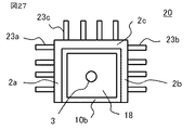
図27は、本発明の実施の形態9によるパワーモジュールの金属ベース側から見た底面図である。図27のパワーモジュール20は、樹脂筐体7の端部からリードフレーム1の端子23が露出していない部分にリブ2がない構造である。図27では、3つのリブ2a、2b、2cが形成され、このリブ2a、2b、2cが形成された樹脂筐体7の端部において、それぞれ端子23a、23b、23cが露出している例を示した。この構造により、実施の形態9のパワーモジュール20は、絶縁距離がない部分の樹脂量を減らすことができ、コストの削減ができる。Embodiment 9
FIG. 27 is a bottom view of the power module according to Embodiment 9 of the present invention as seen from the metal base side. The
実施の形態9のパワーモジュール20と、パワーモジュール20の金属ベース3にグリース14を介して接続されたヒートシンク16を備えたパワー半導体装置40は、リブ部11がベース段差部32の外周を覆うようにパワーモジュール20がヒートシンク16に固定されたので、冷熱環境下で発生するパワーモジュール20のポンピングアウト現象を抑制することができ、グリース14の排出を低減することができ、パワーモジュール20の放熱性低下を抑制できる。
In the
なお、上記各実施の形態においては、パワーモジュール20に搭載される、IGBTやMOSFET等のスイッチング素子や、SBD(Schottky Barrier Diode)やFwD等の整流素子として機能するパワー素子4には、シリコンウエハを基材とした一般的な素子でも良いが、炭化珪素(SiC)や窒化ガリウム(GaN)系材料、またはダイヤモンドといったシリコンと較べてバンドギャップが広い、いわゆるワイドバンドギャップ半導体材料を用いることができる。例えば、スイッチング素子として機能するパワー素子4や、整流素子として機能するパワー素子4に、炭化珪素(SiC)や窒化ガリウム(GaN)系材料又はダイヤモンドを用いた場合、従来から用いられてきたシリコン(Si)で形成された素子よりも電力損失が低いため、パワーモジュール20の高効率化が可能となる。また、耐電圧性が高く、許容電流密度も高いため、パワーモジュール20の小型化が可能となる。さらにワイドバンドギャップ半導体素子は、耐熱性が高いので、高温動作が可能であり、ヒートシンク16の小型化や、水冷部の空冷化も可能となるので、ヒートシンク16を備えたパワー半導体装置40の一層の小型化が可能になる。
In each of the above embodiments, a silicon wafer is used as the
また、本発明は、矛盾のない範囲内において、各実施の形態の内容を自由に組み合わせたり、各実施の形態を適宜、変形、省略したりすることが可能である。 In the present invention, the contents of the respective embodiments can be freely combined, or each embodiment can be appropriately modified or omitted, as long as no contradiction arises.
1…リードフレーム、2、2a、2b、2c、2d…リブ、3…金属ベース、4…パワー素子、7…樹脂筐体、10…本体部、10b…底面、11…リブ部、13…ねじ、14…グリース、16…ヒートシンク、16a…ヒートシンク溝部、18…孔、20…パワーモジュール、26…リブ土台部、27…凸部、31…ヒートシンク土台部、32…ベース段差部、40…パワー半導体装置、50…樹脂部、51…フレーム接触部、51a…フレーム接触部上面、51b…フレーム接触部底面、60…中間製造部品、62…金型、65a、65b…端子開口、66…金属ベース配置部、67a、67b…ピン開口、69…リブ端部形成部、71…突き出しピン、101…窪み、h1、h4、h6、h8、h9…リブ高さ、wb1、wb2…リブ根元幅、hm8…本体上面側高さ、hm9…本体リブ側高さ
DESCRIPTION OF
Claims (19)
前記樹脂筐体は、
前記パワー素子及び前記リードフレームの一部が内部に配置されると共に、底面において前記金属ベースの一面が露出した本体部と、
前記本体部の前記底面において、前記金属ベースの外周を包囲するように設置されると共に、前記本体部の前記底面から当該底面に垂直な方向に突出して設けられたリブ部を備え、
前記リブ部は、前記底面から突出した端部に窪みを有するパワーモジュール。 A power element, a metal base that dissipates heat from the power element, a lead frame electrically connected to an electrode of the power element, and a surface of the metal base and a part of the lead frame are exposed And a resin housing for sealing the power element, wherein the power module comprises:
The resin case is
A body portion in which the power element and a part of the lead frame are disposed inside, and one surface of the metal base is exposed at the bottom surface;
The bottom surface of the main body portion is provided so as to surround the outer periphery of the metal base, and includes a rib portion provided to project from the bottom surface of the main body portion in a direction perpendicular to the bottom surface.
The said rib part is a power module which has a hollow in the edge part which protruded from the said bottom face .
前記凸部は、短手方向の断面であって前記本体部の前記底面に垂直な断面の形状が、前記リブ土台部に接続した接続幅が前記リブ土台部端部から突出した端部である凸部端部の幅よりも大きいテーパ形状であることを特徴とする請求項5記載のパワーモジュール。 The rib base portion is a cross section in a short direction, and a shape of a cross section perpendicular to the bottom surface of the main body portion is a rib whose end whose connection width connected to the bottom surface of the main body portion protrudes from the bottom surface It has a tapered shape that is larger than the width of the base end,
The convex portion is a cross-section in a short direction, and a cross-sectional shape perpendicular to the bottom surface of the main body portion is an end portion where a connection width connected to the rib base portion protrudes from the rib base portion end portion The power module according to claim 5 , wherein the power module has a tapered shape larger than the width of the convex end.
少なくとも1つの前記リブは、前記本体部の前記底面と当該リブの前記本体部の前記底面から最も遠方の端部との高さであるリブ高さが、他のリブにおける前記リブ高さよりも低いことを特徴とする請求項1から6のいずれか1項に記載のパワーモジュール。 The rib portion has a plurality of ribs,
At least one of the ribs has a rib height which is a height between the bottom surface of the main body portion and an end farthest from the bottom surface of the main body portion of the rib is lower than the rib height of other ribs The power module according to any one of claims 1 to 6 , characterized in that:
前記リブ部は、複数のリブを有し、
複数の前記リブのうち2つは、前記底面の前記長辺の外周側に配置された長辺リブであり、
複数の前記リブのうち他の2つは、前記底面の前記短辺の外周側に配置された短辺リブであり、
前記長辺リブの短手方向における前記本体部の前記底面に接続した接続幅は、前記短辺リブの短手方向における前記本体部の前記底面に接続した接続幅よりも大きいことを特徴とする請求項1から7のいずれか1項に記載のパワーモジュール。 The resin case has a quadrilateral shape in which the bottom surface of the main body has a long side and a short side,
The rib portion has a plurality of ribs,
Two of the plurality of ribs are long side ribs disposed on the outer peripheral side of the long side of the bottom surface,
The other two of the plurality of ribs are short side ribs disposed on the outer peripheral side of the short side of the bottom surface,
The connection width connected to the bottom surface of the main body in the short side direction of the long side rib is larger than the connection width connected to the bottom side of the main body in the short direction of the short side rib The power module according to any one of claims 1 to 7.
前記リードフレームが露出するフレーム接触部における前記底面側であるフレーム接触部底面と前記金属ベースの露出面との、前記樹脂筐体の前記底面に垂直な方向の長さが、前記フレーム接触部における前記底面と反対側の当該樹脂筐体の上面の側であるフレーム接触部上面と前記上面との、前記樹脂筐体の前記底面に垂直な方向の長さよりも短いことを特徴とする請求項1から10のいずれか1項に記載のパワーモジュール。 The resin case is
The length in the direction perpendicular to the bottom surface of the resin casing of the bottom surface side of the frame contact portion on the bottom surface side and the exposed surface of the metal base in the frame contact portion where the lead frame is exposed The upper surface of the frame contact portion on the side of the upper surface of the resin casing opposite to the bottom surface and the upper surface are shorter than the length in the direction perpendicular to the bottom surface of the resin casing. The power module according to any one of 10 .
前記ヒートシンクは、ヒートシンク土台部と、前記金属ベースに前記グリースを介して接続されたベース段差部を備え、
前記パワーモジュールは、前記リブ部が前記ベース段差部の外周を覆うように前記ヒートシンクに固定されたことを特徴とするパワー半導体装置。 A power semiconductor device comprising: the power module according to any one of claims 1 to 13 ; and a heat sink connected to the metal base of the power module via grease.
The heat sink comprises a heat sink base and a base step connected to the metal base via the grease.
The power semiconductor device according to claim 1, wherein the power module is fixed to the heat sink such that the rib portion covers an outer periphery of the base step portion.
前記パワーモジュールは、前記貫通孔に挿入されたねじにより前記ヒートシンクの前記ベース段差部に固定されたことを特徴とする請求項14記載のパワー半導体装置。 The power module has a through hole penetrating the metal base from the top surface opposite to the bottom surface,
The power semiconductor device according to claim 14 , wherein the power module is fixed to the base step portion of the heat sink by a screw inserted into the through hole.
前記ヒートシンクは、前記パワーモジュールのリブ部が挿入される溝部を有し、
前記パワーモジュールは、前記リブ部が前記ヒートシンクの前記溝部に挿入されており、かつ前記貫通孔に挿入されたねじにより前記ヒートシンクに固定されたことを特徴とする請求項14記載のパワー半導体装置。 The power module has a through hole penetrating the metal base from the top surface opposite to the bottom surface,
The heat sink has a groove into which the rib of the power module is inserted,
The power semiconductor device according to claim 14 , wherein the rib is fixed to the groove of the heat sink, and the power module is fixed to the heat sink by a screw inserted into the through hole.
金型は、前記樹脂筐体における前記底面から突出した前記リブ部の端部が形成されるリブ端部形成部に、前記樹脂筐体を押出すピンを挿入するピン開口が複数形成されており、
前記パワー素子と、前記金属ベースと、前記リードフレームを備えた中間製造部品を、前記金属ベースが金属ベース配置部に接触すると共に前記リードフレームの一部が前記金型から露出するように、前記金型に配置する工程と、
前記ピン開口が前記ピンで閉じられた状態で、前記金型にトランスファーモールド樹脂を注入し、前記樹脂筐体を形成する工程と、
前記樹脂筐体を前記金型から取り出す際に、前記ピン開口から前記ピンが前記リブ部の端部における短手方向の幅よりも長い深さまで挿入されて、前記ピンが前記樹脂筐体の前記リブ部を押出すことにより、前記リブ部に窪みを形成する工程と、を含むことを特徴とするパワーモジュール製造方法。 A power module manufacturing method for manufacturing a power module according to any one of claims 1 to 10, comprising:
In the mold, a plurality of pin openings for inserting pins for extruding the resin case are formed in a rib end portion forming portion where an end of the rib portion protruding from the bottom surface of the resin case is formed ,
And the power element, and the metal base, an intermediate manufacturing parts having the lead frame, so that a portion of the lead frame with the metal base comes into contact with the metal base placement portion is exposed from the mold, the Placing in the mold;
Transfer mold resin into the mold in a state where the pin opening is closed by the pin, to form the resin casing;
When taking out the resin case from the mold, the pin is inserted from the pin opening to a depth longer than the width in the short direction at the end of the rib portion, and the pin is inserted into the resin case And a step of forming a recess in the rib portion by extruding the rib portion .
Applications Claiming Priority (3)
| Application Number | Priority Date | Filing Date | Title |
|---|---|---|---|
| JP2016074887 | 2016-04-04 | ||
| JP2016074887 | 2016-04-04 | ||
| PCT/JP2017/012257 WO2017175612A1 (en) | 2016-04-04 | 2017-03-27 | Power module, power semiconductor device, and power module manufacturing method |
Publications (2)
| Publication Number | Publication Date |
|---|---|
| JPWO2017175612A1 JPWO2017175612A1 (en) | 2018-07-26 |
| JP6526323B2 true JP6526323B2 (en) | 2019-06-05 |
Family
ID=60000415
Family Applications (1)
| Application Number | Title | Priority Date | Filing Date |
|---|---|---|---|
| JP2018510542A Active JP6526323B2 (en) | 2016-04-04 | 2017-03-27 | POWER MODULE, POWER SEMICONDUCTOR DEVICE, AND POWER MODULE MANUFACTURING METHOD |
Country Status (5)
| Country | Link |
|---|---|
| US (1) | US10461010B2 (en) |
| JP (1) | JP6526323B2 (en) |
| CN (1) | CN108886036B (en) |
| DE (1) | DE112017001840T5 (en) |
| WO (1) | WO2017175612A1 (en) |
Families Citing this family (18)
| Publication number | Priority date | Publication date | Assignee | Title |
|---|---|---|---|---|
| CN210897246U (en) * | 2017-04-28 | 2020-06-30 | 株式会社村田制作所 | Circuit module |
| JP7221930B2 (en) * | 2017-07-12 | 2023-02-14 | ヒタチ・エナジー・スウィツァーランド・アクチェンゲゼルシャフト | power semiconductor module |
| JP7024269B2 (en) * | 2017-09-12 | 2022-02-24 | 富士電機株式会社 | A method for transporting a semiconductor device, a laminate of semiconductor devices, and a laminate of semiconductor devices. |
| CN112655087A (en) * | 2018-09-06 | 2021-04-13 | 三菱电机株式会社 | Power semiconductor device, method for manufacturing same, and power conversion device |
| US11373939B2 (en) * | 2018-09-26 | 2022-06-28 | Semiconductor Components Industries, Llc | Quad leadframe packages and related methods |
| WO2020144814A1 (en) * | 2019-01-10 | 2020-07-16 | 三菱電機株式会社 | Semiconductor device |
| JP7187716B2 (en) | 2019-04-25 | 2022-12-12 | アメリカン アクスル アンド マニュファクチャリング,インコーポレイテッド | electric drive module |
| DE112019007411T5 (en) * | 2019-06-06 | 2022-02-17 | Mitsubishi Electric Corporation | SEMICONDUCTOR MODULE AND POWER CONVERSION DEVICE |
| JP7178978B2 (en) * | 2019-10-24 | 2022-11-28 | 三菱電機株式会社 | Semiconductor device and method for manufacturing semiconductor device |
| US11276624B2 (en) * | 2019-12-17 | 2022-03-15 | Infineon Technologies Austria Ag | Semiconductor device power metallization layer with stress-relieving heat sink structure |
| CN114902400A (en) * | 2020-01-08 | 2022-08-12 | 三菱电机株式会社 | Semiconductor device and method for manufacturing semiconductor device |
| DE102020208434A1 (en) | 2020-07-06 | 2022-01-13 | Zf Friedrichshafen Ag | Half-bridge module for an inverter of an electric drive of an electric vehicle or a hybrid vehicle, method for its production, inverter for an electric drive of an electric vehicle or a hybrid vehicle and tool for transfer molding the half-bridge module |
| DE102020129423B4 (en) * | 2020-11-09 | 2024-03-07 | Infineon Technologies Ag | Linear spacer for spacing a carrier of a package |
| DE102020130612A1 (en) | 2020-11-19 | 2022-05-19 | Infineon Technologies Ag | Package with an electrically insulating carrier and at least one step on the encapsulant |
| CN112864113A (en) * | 2021-02-10 | 2021-05-28 | 华为技术有限公司 | Power device, power device assembly and related device |
| CN113394201B (en) * | 2021-06-21 | 2022-08-09 | 深圳市好年华电子有限公司 | Multi-chip integrated circuit packaging structure |
| JP2023007133A (en) * | 2021-07-01 | 2023-01-18 | 日立Astemo株式会社 | Power semiconductor device |
| EP4177942A1 (en) * | 2021-10-18 | 2023-05-10 | American Axle & Manufacturing, Inc. | Electrical assembly having a heat sink that is unitarily and integrally formed with a lead of a power semiconductor |
Family Cites Families (20)
| Publication number | Priority date | Publication date | Assignee | Title |
|---|---|---|---|---|
| JPS53108872U (en) * | 1977-02-07 | 1978-08-31 | ||
| JPH09260550A (en) * | 1996-03-22 | 1997-10-03 | Mitsubishi Electric Corp | Semiconductor device |
| JP3910383B2 (en) | 2001-07-17 | 2007-04-25 | 株式会社日立製作所 | Power module and inverter |
| JP4177571B2 (en) | 2001-09-20 | 2008-11-05 | 三菱電機株式会社 | Semiconductor device |
| JP3740116B2 (en) * | 2002-11-11 | 2006-02-01 | 三菱電機株式会社 | Molded resin encapsulated power semiconductor device and manufacturing method thereof |
| JP3740117B2 (en) * | 2002-11-13 | 2006-02-01 | 三菱電機株式会社 | Power semiconductor device |
| JP4594237B2 (en) * | 2003-09-04 | 2010-12-08 | パナソニック株式会社 | Semiconductor device |
| DE102005010311A1 (en) * | 2005-03-03 | 2006-09-14 | Atmel Germany Gmbh | Method and mold for producing an optical semiconductor module |
| JP2007073743A (en) * | 2005-09-07 | 2007-03-22 | Denso Corp | Semiconductor device |
| KR101221805B1 (en) * | 2006-03-03 | 2013-01-14 | 페어차일드코리아반도체 주식회사 | Package and package assembly for power device |
| JP2008118067A (en) * | 2006-11-08 | 2008-05-22 | Hitachi Ltd | Power module and motor-integrated controlling device |
| US8207607B2 (en) | 2007-12-14 | 2012-06-26 | Denso Corporation | Semiconductor device with resin mold |
| JP4760876B2 (en) * | 2008-08-22 | 2011-08-31 | 株式会社デンソー | Electronic device and manufacturing method thereof |
| JP5669866B2 (en) * | 2011-02-09 | 2015-02-18 | 三菱電機株式会社 | Power semiconductor module |
| JP5936310B2 (en) | 2011-03-17 | 2016-06-22 | 三菱電機株式会社 | Power semiconductor module and its mounting structure |
| JP5623367B2 (en) * | 2011-10-21 | 2014-11-12 | 三菱電機株式会社 | Semiconductor device and semiconductor device module |
| JP2013157550A (en) * | 2012-01-31 | 2013-08-15 | Rohm Co Ltd | Power module semiconductor device and method of manufacturing the same |
| KR101388815B1 (en) * | 2012-06-29 | 2014-04-23 | 삼성전기주식회사 | Semiconductor package |
| CN106165089B (en) | 2014-03-28 | 2020-06-09 | 三菱电机株式会社 | Semiconductor module and driving device mounted with semiconductor module |
| JP6470938B2 (en) | 2014-10-06 | 2019-02-13 | 日立オートモティブシステムズ株式会社 | Power module and power converter |
-
2017
- 2017-03-27 JP JP2018510542A patent/JP6526323B2/en active Active
- 2017-03-27 WO PCT/JP2017/012257 patent/WO2017175612A1/en active Application Filing
- 2017-03-27 DE DE112017001840.4T patent/DE112017001840T5/en active Pending
- 2017-03-27 US US16/070,839 patent/US10461010B2/en active Active
- 2017-03-27 CN CN201780021845.0A patent/CN108886036B/en active Active
Also Published As
| Publication number | Publication date |
|---|---|
| US10461010B2 (en) | 2019-10-29 |
| CN108886036A (en) | 2018-11-23 |
| WO2017175612A1 (en) | 2017-10-12 |
| DE112017001840T5 (en) | 2018-12-27 |
| CN108886036B (en) | 2022-06-24 |
| US20190067154A1 (en) | 2019-02-28 |
| JPWO2017175612A1 (en) | 2018-07-26 |
Similar Documents
| Publication | Publication Date | Title |
|---|---|---|
| JP6526323B2 (en) | POWER MODULE, POWER SEMICONDUCTOR DEVICE, AND POWER MODULE MANUFACTURING METHOD | |
| KR101221805B1 (en) | Package and package assembly for power device | |
| JP4455488B2 (en) | Semiconductor device | |
| JP5873998B2 (en) | Semiconductor device and manufacturing method thereof | |
| TWI404177B (en) | Electric power semiconductor circuit device and method for making same | |
| KR101915873B1 (en) | Power semiconductor device and method for manufacturing same | |
| US7902653B2 (en) | Semiconductor module | |
| US9754855B2 (en) | Semiconductor module having an embedded metal heat dissipation plate | |
| JPH09153572A (en) | Semiconductor device | |
| CN108292631B (en) | Semiconductor module | |
| JP6707328B2 (en) | Power module, heat dissipation structure of power module, and joining method of power module | |
| JP2014216459A (en) | Semiconductor device | |
| JP2014187209A (en) | Semiconductor device | |
| JP2015046476A (en) | Power semiconductor device and method of manufacturing the same | |
| CN106298700B (en) | Semiconductor device with a plurality of semiconductor chips | |
| CN111095537B (en) | Semiconductor device and power conversion device provided with same | |
| US10777476B2 (en) | Semiconductor device | |
| JP7379886B2 (en) | semiconductor equipment | |
| JP2012209470A (en) | Semiconductor device, semiconductor device module, and manufacturing method of the semiconductor device | |
| KR101255930B1 (en) | Power Module Package and Method for Manufacturing the same | |
| JP2010050395A (en) | Semiconductor device, and method of manufacturing the same | |
| CN219658693U (en) | Power semiconductor module | |
| WO2019021507A1 (en) | Semiconductor device and semiconductor module | |
| JP7136367B2 (en) | semiconductor package | |
| US20230067725A1 (en) | Semiconductor device and method of manufacturing semiconductor device |
Legal Events
| Date | Code | Title | Description |
|---|---|---|---|
| A521 | Request for written amendment filed |
Free format text: JAPANESE INTERMEDIATE CODE: A523 Effective date: 20180406 |
|
| A621 | Written request for application examination |
Free format text: JAPANESE INTERMEDIATE CODE: A621 Effective date: 20180406 |
|
| TRDD | Decision of grant or rejection written | ||
| A01 | Written decision to grant a patent or to grant a registration (utility model) |
Free format text: JAPANESE INTERMEDIATE CODE: A01 Effective date: 20190409 |
|
| A61 | First payment of annual fees (during grant procedure) |
Free format text: JAPANESE INTERMEDIATE CODE: A61 Effective date: 20190507 |
|
| R151 | Written notification of patent or utility model registration |
Ref document number: 6526323 Country of ref document: JP Free format text: JAPANESE INTERMEDIATE CODE: R151 |
|
| R250 | Receipt of annual fees |
Free format text: JAPANESE INTERMEDIATE CODE: R250 |
|
| R250 | Receipt of annual fees |
Free format text: JAPANESE INTERMEDIATE CODE: R250 |