JP6519045B2 - Glass panel manufacturing method and liquid crystal panel manufacturing method - Google Patents
Glass panel manufacturing method and liquid crystal panel manufacturing method Download PDFInfo
- Publication number
- JP6519045B2 JP6519045B2 JP2017102308A JP2017102308A JP6519045B2 JP 6519045 B2 JP6519045 B2 JP 6519045B2 JP 2017102308 A JP2017102308 A JP 2017102308A JP 2017102308 A JP2017102308 A JP 2017102308A JP 6519045 B2 JP6519045 B2 JP 6519045B2
- Authority
- JP
- Japan
- Prior art keywords
- etching
- glass
- liquid crystal
- line
- substrate
- Prior art date
- Legal status (The legal status is an assumption and is not a legal conclusion. Google has not performed a legal analysis and makes no representation as to the accuracy of the status listed.)
- Active
Links
Images


Description
本発明は、多面取り用ガラス母材から所望形状のガラスパネルや所望形状の液晶パネルを複数得るためのガラスパネル製造方法および液晶パネル製造方法に関する。 The present invention relates to a glass panel manufacturing method and a liquid crystal panel manufacturing method for obtaining a plurality of glass panels of a desired shape and a liquid crystal panel of a desired shape from a glass substrate for multiple chamfers.
一般的に、液晶パネルやカバーガラス等のガラスパネルの製造時には、多面取り用ガラス母材から所望形状の複数のガラスパネルを得るような処理が行われる。例えば、液晶パネルの製造においては、1組のガラス母材で同時に複数の液晶パネルを製造し、その後にガラス母材を単個の液晶パネルに分断するという手法(いわゆる多面取り)が広く採用されてきた。そして、ガラス母材を分断する際には、スクライブブレーク、レーザアブレーション加工、エッチング処理といった手法が用いられることが多かった。 Generally, at the time of manufacture of glass panels, such as a liquid crystal panel and cover glass, processing which obtains a plurality of glass panels of a desired shape from a glass base material for multiple chamfers is performed. For example, in the manufacture of liquid crystal panels, a method (so-called multi-chamfering) in which a plurality of liquid crystal panels are simultaneously manufactured from one set of glass base materials and then the glass base materials are divided into single liquid crystal panels It has And when dividing a glass base material, methods, such as a scribe break, a laser ablation process, and an etching process, were used in many cases.
ところが、スクライブブレークを採用した場合には、丸みを持った輪郭を有するガラスパネルを形成することが困難であった。また、レーザアブレーション加工では、加工速度が遅かったり、アブレーションデブリによる汚損が生じたりするといった不具合が発生し易かった。 However, when a scribe break is adopted, it is difficult to form a glass panel having a rounded contour. Further, in the laser ablation process, problems such as a slow processing speed and contamination due to ablation debris easily occurred.
そこで、従来、多面取り用ガラス母材をエッチング処理によって分断することによって複数のガラスパネルを得る技術が注目されるようになってきた。エッチング処理は、所望形状のカバーガラスを得るために利用されるようになり、最近では、アレイ基板およびカラーフィルタ基板を貼り合せてなる液晶パネルを多面取りするための多面取り用ガラス母材から所定形状の液晶パネルを複数得る際にもエッチング処理が用いられるようになってきている(例えば、特許文献1参照。)。 Therefore, in the past, techniques for obtaining a plurality of glass panels by dividing a glass substrate for multiple chamfers by etching processing have come to be noted. The etching process is used to obtain a cover glass having a desired shape, and recently, it is specified from a glass base material for multiple chamfering for multiple chamfering of a liquid crystal panel formed by bonding an array substrate and a color filter substrate. The etching process has come to be used also when obtaining a plurality of liquid crystal panels having a shape (see, for example, Patent Document 1).
しかしながら、エッチング処理においては、ガラスパネルの厚み方向にエッチングが進行するのに加えて、これに直交する方向にもエッチングが進行するサイドエッチングが発生する。このため、エッチング処理においては、ガラスパネルの切断面を主面とほぼ直角になるように形成することが困難になる。例えば、液晶パネルをエッチング処理によって多面取りする場合には、ガラス母材の厚み方向に直交する方向に進行するサイドエッチングの影響を考慮して、ガラス母材において各液晶パネル間にスペースを設ける必要があるため、多面取り効率が悪くなることがあった。 However, in the etching process, in addition to the etching progressing in the thickness direction of the glass panel, side etching occurs in which the etching progresses also in the direction orthogonal to this. Therefore, in the etching process, it is difficult to form the cut surface of the glass panel so as to be substantially perpendicular to the main surface. For example, when the liquid crystal panel is chamfered by etching, it is necessary to provide a space between the liquid crystal panels in the glass base material in consideration of the influence of side etching which proceeds in the direction orthogonal to the thickness direction of the glass base material. There are cases where the efficiency of multiple beveling is worse.
本発明の目的は、エッチング処理に伴うサイドエッチングの影響を最小限に抑制することが可能なガラスパネル製造方法および液晶パネル製造方法を提供することである。 An object of the present invention is to provide a glass panel manufacturing method and a liquid crystal panel manufacturing method capable of minimizing the influence of side etching associated with etching processing.
本発明に係るガラスパネル製造方法は、ガラスパネルを多面取りするための多面取り用ガラス母材から所望形状のガラスパネルを複数得るための方法である。このガラスパネル製造方法は、透明の耐エッチング層を形成するステップ、レーザ走査ステップ、およびエッチングステップを少なくとも含む。 The glass panel manufacturing method which concerns on this invention is a method for obtaining two or more glass panels of a desired shape from the glass base material for multiple chamfers for chamfering a glass panel multiple. The glass panel manufacturing method includes at least a step of forming a transparent etching resistant layer, a laser scanning step, and an etching step.
透明の耐エッチング層を形成するステップでは、多面取り用ガラスパネルの表面に対して、耐エッチング性を備えた透明の耐エッチング層を形成する。耐エッチング層の代表例としては、ガラスをエッチングするフッ酸を含むエッチング液に対する耐性を備えた透明の樹脂材料からなる耐エッチングフィルムが挙げられる。耐エッチングフィルムは、透明の耐エッチング性を有する接着剤を介して貼付しても良いし、自己粘着性を備えたものを用いても良い。耐エッチングフィルム以外にも、耐エッチング性を備えた透明のレジスト材料やその他の透明のマスキング部材を用いて耐エッチング層を形成することが可能である。 In the step of forming a transparent etching resistant layer, a transparent etching resistant layer having etching resistance is formed on the surface of the glass panel with multiple bevels. A representative example of the etching resistant layer is an etching resistant film made of a transparent resin material resistant to an etching solution containing hydrofluoric acid for etching glass. The etching resistant film may be attached via a transparent etching resistant adhesive, or one having self-adhesiveness may be used. Besides the etching resistant film, it is possible to form the etching resistant layer using a transparent resist material with etching resistance and other transparent masking members.
レーザ走査ステップにおいては、取り出すべきガラスパネルの形状に対応する形状切断予定線に沿ってレーザを走査することによって、形状切断予定線に沿って、耐エッチング層を除去しかつ多面取り用ガラス母材にエッチングされ易い性質の改質ラインが形成される。耐エッチング層が形状切断予定線に沿って除去されることにより、形状切断予定線に沿って耐エッチング層の開口部が形成されることになり、その結果、多面取り用ガラス母材の改質ライン形成位置が露出する。特に、同じレーザビームによって耐エッチング層の除去および改質ラインの形成を行っているため、耐エッチング層の開口位置と改質ラインの形成位置とがずれることを防止可能になる。改質ラインを形成する手法の代表例としては、ピコ秒レーザまたはフェムト秒レーザによるフィラメント加工が挙げられる。改質ラインの幅は、概ね10μm以下に設定することが好ましい。 In the laser scanning step, the etching resistant layer is removed along the planned shape cutting line by scanning the laser along the planned shape cutting line corresponding to the shape of the glass panel to be taken out, and the glass substrate for multiple chamfers The reformed line of the nature which is easy to be etched is formed. By removing the etching resistant layer along the planned shape cutting line, the opening of the etching resistant layer is formed along the planned shape cutting line, and as a result, modification of the glass substrate for multiple beveling The line formation position is exposed. In particular, since the removal of the etching resistant layer and the formation of the reforming line are performed by the same laser beam, it is possible to prevent the shift between the opening position of the etching resistant layer and the forming position of the modifying line. Representative examples of the method of forming the reforming line include filament processing with a picosecond laser or a femtosecond laser. The width of the reforming line is preferably set to about 10 μm or less.
エッチングステップにおいては、レーザ走査ステップ後に、多面取り用ガラス母材をエッチング液に接触させることによって改質ラインがエッチングされる。改質ラインに沿ってエッチング液が浸透し易くなっており、エッチング処理の進行が容易で短時間化されるため、サイドエッチングの影響を最小化することが可能になる。 In the etching step, after the laser scanning step, the reforming line is etched by bringing the glass substrate for multiple beveling into contact with the etching solution. Since the etchant easily penetrates along the reforming line and the progress of the etching process is easy and shortened, the influence of side etching can be minimized.
上述のガラスパネル製造方法において、透明の耐エッチング層が、50μm〜100μmの薄型透明フィルムであることが好ましい。耐エッチング層を50μm〜100μm程度まで薄型化することにより、剥離を行い易くなる。また、レーザビームが通過する際の光学的影響も少なくなるため、レーザビームの焦点やビームプロファイルを正確に調整し易くなる。一方で、形状切断予定線に沿って改質ラインが形成されているため、エッチング処理を迅速に行うことが可能であり、要求される耐エッチング性能が低く抑えられる。このため、通常のエッチング処理よりも耐エッチングフィルムは薄くても問題はない。なお、薄型透明フィルムの特性はガラスの特性と類似している方がレーザ光の焦点精度向上の観点からさらに好ましいと言える。 In the glass panel manufacturing method described above, the transparent etching resistant layer is preferably a thin transparent film of 50 μm to 100 μm. By thinning the etching resistant layer to about 50 μm to 100 μm, it becomes easy to peel off. In addition, since the optical effect when the laser beam passes is also reduced, it becomes easy to accurately adjust the focus and beam profile of the laser beam. On the other hand, since the reforming line is formed along the planned shape cutting line, the etching process can be performed quickly, and the required etching resistance can be suppressed to a low level. Therefore, there is no problem even if the etching resistant film is thinner than the usual etching process. In addition, it can be said that it is more preferable from the viewpoint of the focus precision improvement of a laser beam that the characteristic of a thin transparent film to be similar to the characteristic of glass.
さらに、この発明に係る液晶パネル製造方法は、アレイ基板およびカラーフィルタ基板を貼り合せてなる液晶パネルを多面取りするための多面取り用ガラス母材から所定形状の液晶パネルを複数得るためのものである。この液晶パネル製造方法は、透明の耐エッチング層を形成するステップ、レーザ走査ステップ、およびエッチングステップを少なくとも含んでいる。 Furthermore, the liquid crystal panel manufacturing method according to the present invention is to obtain a plurality of liquid crystal panels having a predetermined shape from a multiple bevel glass base material for multi beveling a liquid crystal panel formed by bonding an array substrate and a color filter substrate. is there. This liquid crystal panel manufacturing method includes at least a step of forming a transparent etching resistant layer, a laser scanning step, and an etching step.
透明の耐エッチング層を形成するステップにおいては、アレイ基板およびカラーフィルタ基板に対して、耐エッチング性を備えた透明のエッチング層を貼付する。上述と同様、耐エッチング層の代表例としては、ガラスをエッチングするフッ酸を含むエッチング液に対する耐性を備えた透明の樹脂材料からなる耐エッチングフィルムが挙げられる。耐エッチングフィルムは、透明の耐エッチング性を有する接着剤を介して貼付しても良いし、自己粘着性を備えたものを用いても良い。耐エッチングフィルム以外にも、耐エッチング性を備えた透明のレジスト材料やその他の透明のマスキング部材を用いて耐エッチング層を形成することが可能である。 In the step of forming a transparent etching resistant layer, a transparent etching layer having etching resistance is attached to the array substrate and the color filter substrate. As described above, as a representative example of the etching resistant layer, an etching resistant film made of a transparent resin material having resistance to an etching solution containing hydrofluoric acid for etching glass can be mentioned. The etching resistant film may be attached via a transparent etching resistant adhesive, or one having self-adhesiveness may be used. Besides the etching resistant film, it is possible to form the etching resistant layer using a transparent resist material with etching resistance and other transparent masking members.
レーザ走査ステップにおいては、液晶パネルの形状に対応する形状切断予定線に沿ってレーザを走査することによって、形状切断予定線に沿って、耐エッチング層を除去しかつ多面取り用ガラス母材にエッチングされ易い性質の改質ラインを形成する。さらに、エッチングステップにおいては、レーザ走査ステップ後に、多面取り用ガラス母材をエッチング液に接触させることによって改質ラインをエッチングする。 In the laser scanning step, the etching resistant layer is removed along the planned shape cutting line and the glass substrate for multiple chamfering is etched by scanning the laser along the planned shape cutting line corresponding to the shape of the liquid crystal panel. Form a reforming line of a nature that is easy to Furthermore, in the etching step, after the laser scanning step, the modified line is etched by bringing the multiple bevel glass substrate into contact with the etching solution.
この液晶パネル製造方法においては、アレイ基板およびカラーフィルタ基板にそれぞれ改質ラインが形成されるため、それぞれの基板をサイドエッチングの影響を最小化しつつ、エッチング処理によって多面取り用ガラス母材を分断することが可能になる。 In this liquid crystal panel manufacturing method, modification lines are respectively formed on the array substrate and the color filter substrate, and therefore the multiple bevel glass base material is divided by etching while minimizing the influence of side etching on each substrate. It becomes possible.
上述のレーザ走査ステップにおいて、アレイ基板およびカラーフィルタ基板に挟まれる液晶層において気泡発生等の不具合が生じる場合には、形状切断予定線に沿って、耐エッチングフィルムを除去しかつ改質ラインをアレイ基板またはカラーフィルタ基板のいずれか一方にのみ形成すると良い。この方法を採用することにより、液晶層に対するレーザビームの熱的影響等を減少させることが可能となるため、液晶層において気泡が発生するといった不具合が生じにくくなる。 If defects such as air bubbles occur in the liquid crystal layer sandwiched between the array substrate and the color filter substrate in the above-mentioned laser scanning step, the etching resistant film is removed along the shape cutting lines and the reforming lines are arrayed. It is preferable to form on only one of the substrate and the color filter substrate. By adopting this method, it is possible to reduce the thermal influence and the like of the laser beam on the liquid crystal layer, so it becomes difficult to cause a problem such as generation of bubbles in the liquid crystal layer.
また、前段落に記載の方法では、多面取り用ガラス部材の分断が困難になる場合には、上述のレーザ走査ステップにおいて、形状切断予定線に沿って、耐エッチングフィルムを除去しかつ改質ラインをアレイ基板またはカラーフィルタ基板のいずれか一方にのみ形成し、その後に反対側からレーザを走査することによって改質ラインをアレイ基板またはカラーフィルタ基板のいずれか他方にも形成すると良い。 In the method described in the preceding paragraph, when it becomes difficult to divide the glass member for multiple chamfers, the etching resistant film is removed along the shape cutting planned line in the above-mentioned laser scanning step, and the reforming line is modified. It is preferable to form the modified line on either the array substrate or the color filter substrate by scanning the laser from the opposite side only on either the array substrate or the color filter substrate.
エッチング処理後には、形状切断予定線において実質的にほぼ切断された状態になっているため、わずかな機械的圧力や熱的応力を加えることによって完全な切断を実現することが可能である。微小な押圧力を加えたり、微小な超音波振動を与えたり、加熱をしたりすることによって、多面取り用ガラス母材を汚損することなく、完全な切断を実現することが可能である。 After the etching process, it is possible to achieve complete cutting by applying a slight mechanical pressure or thermal stress, since it is in a substantially substantially cut state at the shape cutting scheduled line. It is possible to realize complete cutting without staining the multi-faceted glass base material by applying a minute pressing force, giving a minute ultrasonic vibration, or heating.
上述のガラスパネル製造方法および液晶パネル製造方法において、改質ラインが、パルスレーザのビームによって形成された複数の貫通孔または複数の改質孔を有するミシン目状を呈することが好ましい。ガラスパネルや液晶パネルの形状切断予定線をパルスレーザによって加工するため、ガラスパネルや液晶パネルの輪郭に複雑な曲線や微小な曲線部分が含まれていたり、ガラスパネルや液晶パネルに開口部が形成されていたりする場合であっても、適切な加工を実現することが可能になる。 In the above-described glass panel manufacturing method and liquid crystal panel manufacturing method, it is preferable that the reforming line has a perforated shape having a plurality of through holes or a plurality of reforming holes formed by a beam of a pulse laser. In order to process the shape cutting scheduled line of a glass panel or a liquid crystal panel with a pulse laser, the contour of the glass panel or the liquid crystal panel includes a complicated curve or a minute curved portion, or an opening is formed in the glass panel or the liquid crystal panel Even if it is done, it becomes possible to realize appropriate processing.
この発明によれば、ガラスパネル製造方法および液晶パネル製造方法においてエッチング処理に伴うサイドエッチングの影響を最小限に抑制することが可能になる。 According to the present invention, it is possible to minimize the influence of side etching accompanying the etching process in the glass panel manufacturing method and the liquid crystal panel manufacturing method.
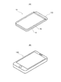
まず、図1〜図3を用いて本発明に係るガラスパネル製造方法の一実施形態を説明する。図1(A)は、ガラスパネル2を多面取りするための多面取り用ガラス母材4の概略を示している。多面取り用ガラス母材4から所望形状のガラスパネル2を複数得るために、まず、図1(B)に示すように、透明の耐エッチングフィルム6が多面取り用ガラス母材4の少なくとも両主面に貼付される。この実施形態では、耐エッチングフィルム6として、透明のポリエチレン樹脂材料を採用している。ただし、耐エッチングフィルム6として、透明のポリプロピレンや透明ポリ塩化ビニルやオレフィン系樹脂等を採用することも可能である。
First, an embodiment of a glass panel manufacturing method according to the present invention will be described using FIGS. 1 to 3. FIG. 1A shows an outline of a multiple
この実施形態では、耐エッチングフィルム6が本発明に係る耐エッチング層に対応している。耐エッチングフィルム6は、厚みが100μm以下の薄型のものが用いられる。薄型化することにより剥離を行い易くなり、かつ、レーザビームが通過する際の光学的影響も少なくなることを考慮すると、耐エッチングフィルム6の厚みは耐エッチング性能を満たすために必要な最小限の厚みにすることが好ましい。よって、好ましくは耐エッチングフィルム6の厚みを75μm以下に抑え、さらに好ましくは、耐エッチングフィルム6の厚みを60μm以下にすると良い。後述するように、この実施形態では、改質ラインが形成されることによってエッチング処理が迅速化するため、耐エッチングフィルム6を超薄化してもデメリットが発生しにくい。
In this embodiment, the etching
多面取り用ガラス母材4に耐エッチングフィルム6が貼付された後に、図1(C)に示すレーザ走査ステップに移行する。レーザ走査ステップにおいては、取り出すべきガラスパネル2の形状に対応する形状切断予定線に沿ってレーザビームの走査が行われる。この結果、形状切断予定線に沿って、耐エッチングフィルムが除去されて開口部が形成される。
After the etching
さらに、図2(A)〜図2(C)に示すように、多面取り用ガラス母材4にエッチングされ易い性質の改質ライン20が形成される。耐エッチングフィルム6が形状切断予定線に沿って除去されることにより、形状切断予定線に沿って耐エッチングフィルム6の開口部が形成されることになり、その結果、図2(C)に示すように、多面取り用ガラス母材4の改質ライン20の形成位置が外部に露出することになる。この実施形態では、ピコ秒レーザによるフィラメント加工が採用されており、改質ライン20の幅は、概ね10μm以下になるように設定されている。
Furthermore, as shown to FIG. 2 (A)-FIG.2 (C), the
レーザ走査ステップが終了するとエッチングステップに移行する。レーザ走査ステップ後に、多面取り用ガラス母材4をエッチング液に接触させることによって改質ライン20がエッチングされる。改質ライン20に沿ってエッチング液が浸透し易くなっているため、サイドエッチングが大きく進行する前にエッチング処理を終了することが可能になる。その結果、エッチング処理に伴うサイドエッチングの影響を最小限に抑制しつつ、多面取り用ガラス母材4から複数のガラスパネル2を取り出すことが可能になる。なお、エッチングステップにおいて用いられる構成等については、後述の液晶パネルの製造の際にまとめて説明を行うため、ここではその説明を省略している。
When the laser scanning step is finished, the etching step is started. After the laser scanning step, the reforming
続いて、本発明に係る液晶パネルの製造方法の一実施形態を説明する。図4(A)は、本発明の一実施形態に係る液晶パネル10の概略構成を示している。同図に示すように、液晶パネル10は、アレイ基板12およびカラーフィルタ基板14が液晶層を挟んで貼り合わされるように構成されている。アレイ基板12およびカラーフィルタ基板14の構成は、公知の構成と同様の構成が採用可能であるため、ここでは説明を省略する。
Subsequently, an embodiment of a method of manufacturing a liquid crystal panel according to the present invention will be described. FIG. 4A shows a schematic configuration of a
アレイ基板12は、カラーフィルタ基板14と貼り合わされる領域から延び出すように設けられた電極端子部122を有している。この電極端子部122には、複数の電気回路が接続され、液晶パネル10と、それらの電気回路とが筐体に収納されることによって、例えば、図4(B)に示すようなスマートフォン100が構成される。
The
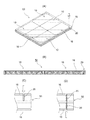
続いて、液晶パネル10を製造する方法の一例について説明する。図5(A)および図5(B)に示すように、一般的に、液晶パネル10は、これを複数含んだ多面取り用ガラス母材50として製造され、多面取り用ガラス母材50を分断することによって、単個の液晶パネル10が得られる。この実施形態では、便宜上、6つの液晶パネル10が3行2列のマトリクス状に配置された多面取り用ガラス母材50に対する処理について説明するが、多面取り用ガラス母材50に含まれる液晶パネル10の数は適宜増減することが可能である。
Subsequently, an example of a method of manufacturing the
多面取り用ガラス母材50は、まず、図6(A)および図6(B)に示すように、両方の主面に耐エッチング性を備えた透明の耐エッチングフィルム16が貼付される。ここでは、耐エッチングフィルム16として、厚みが50〜75μmのポリエチレンを採用している。ただし、耐エッチングフィルム16の構成はこれには限定されない。例えば、ポリプロピレンやポリ塩化ビニルやオレフィン系樹脂等のように透明性を備え、かつ、ガラスをエッチングするエッチング液に対する耐性を備えたものであれば適宜選択して採用することも可能である。
First, as shown in FIG. 6A and FIG. 6B, a transparent etching
多面取り用ガラス母材50は、続いて、図7(A)および図7(B)に示すように、液晶パネル10の形状(輪郭)に対応する形状切断予定線に沿って改質ライン20が形成される。この改質ライン20は、例えば、ピコ秒レーザまたはフェムト秒レーザ等のパルスレーザから照射される光ビームパルス(ビーム径は1〜5μm程度)によって形成される複数のフィラメント層を配列したフィラメントアレイである。
Subsequently, as shown in FIGS. 7A and 7B, the
ピコレーザからの光ビームは、一般的には、少なくともアレイ基板12、カラーフィルタ基板14、および耐エッチングフィルム16の厚みを合計した厚みよりも広範囲にわたって均一で強い光強度になるようなビームプロファイルを備えていることが好ましい。このような構成を採用する場合には、アレイ基板12、カラーフィルタ基板14、および耐エッチングフィルム16のすべてに対してエネルギを伝達することが可能になり、耐エッチングフィルム16の除去および液晶パネル10を取り出すための改質ライン20の形成を同時に行うことが可能になる。
The light beam from the picolaser generally has a beam profile such that the light intensity is uniform and strong over a wider range than the total thickness of at least the
ただし、アレイ基板12、カラーフィルタ基板14、および耐エッチングフィルム16を同時に1つのレーザビームによって処理することによって液晶層に不具合が生じる場合には、図7(C)および図7(D)に示すようなレーザ加工を採用することにより、このような不具合の発生を抑制することが可能となる。すなわち図7(C)に示すように、アレイ基板12側からアレイ基板12のみに改質ライン20を形成されるように焦点調整および強度調整をした上でレーザを走査し、液晶層近傍にエネルギが伝達しにくくすると良い。この状態で、物理的作用または熱的作用を加えることによって多面取り用ガラス母材50の分断が可能であれば、レーザ加工はここで終了する。
However, when problems occur in the liquid crystal layer by treating the
一方で、この状態では多面取り用ガラス母材50の分断が困難な場合には、図7(D)に示すように、今度は反対側となるカラーフィルタ基板14側からカラーフィルタ基板14のみに改質ライン20を形成するように焦点調整および強度調整をした上でレーザを走査すると良い。図7(D)に示す処理を行うことにより、レーザ加工の工程数が増加するものの、液晶層における不具合の発生を抑制しつつ、多面取り用ガラス母材50の分断を容易に行うことが可能になる。
On the other hand, if it is difficult to divide the multiple bevel
この実施形態においても、改質ライン20は、上述の図2(A)にて示したものと同様に、複数の貫通孔または改質層を有するミシン目状を呈している。改質ライン20は、多面取り用ガラス母材50における他の箇所よりもエッチングされ易い性質を有している。もちろん、改質ライン20の形状は、この形状には限定されるものではなく、これ以外の形状を呈するものであっても良い。
Also in this embodiment, the reforming
上述のレーザ加工が終わると、図8に示すように、多面取り用ガラス母材50は、エッチング装置300に導入され、フッ酸および塩酸等を含むエッチング液によってエッチング処理が施される。エッチング装置300では、搬送ローラによって多面取り用ガラス母材50を搬送しつつ、エッチングチャンバ内で多面取り用ガラス母材50の片面または両面にエッチング液を接触させることによって、多面取り用ガラス母材50に対するエッチング処理が行われる。なお、エッチング装置300におけるエッチングチャンバの後段には、多面取り用ガラス母材50に付着したエッチング液を洗い流すための洗浄チャンバが設けられているため、多面取り用ガラス母材50はエッチング液が取り除かれた状態でエッチング装置300から排出される。
After the above-mentioned laser processing is completed, as shown in FIG. 8, the glass substrate for
多面取り用ガラス母材50にエッチング液を接触させる手法の一例として、図9(A)に示すように、エッチング装置300の各エッチングチャンバ302において、多面取り用ガラス母材50に対してエッチング液をスプレイするスプレイエッチングが挙げられる。また、スプレイエッチングに代えて、図9(B)に示すように、オーバーフロー型のエッチングチャンバ304において、オーバーフローしたエッチング液に接触しながら多面取り用ガラス母材50が搬送される構成を採用することも可能である。
As an example of the method for bringing the etching solution into contact with the
さらには、図9(C)に示すように、エッチング液が収納されたエッチング槽306に、キャリアに収納された単数または複数の多面取り用ガラス母材50を浸漬されるディップ式のエッチングを採用することも可能である。
Furthermore, as shown in FIG. 9C, a dip type etching is employed in which one or a plurality of multi-faceted
いずれの場合であっても、エッチング処理中に、形状切断予定線が厚み方向に貫通して、多面取り用ガラス母材50が分断してしまわないようにすることが重要である。このため、エッチング処理中(特にエッチング処理の後半部分)においては、エッチングレートを遅くして、エッチング量を正確に制御する必要がある。この実施形態では、2重量%以下の薄いフッ酸によって、3μm/分以下の遅い速度にてエッチング処理が進行するようにしているが、この手法に限定されるものではない。
In any case, it is important that the planned shape cutting line penetrates in the thickness direction during the etching process so that the multiple bevel
エッチング処理の全体においてエッチングレートを遅くするのではなく、当初は速めのエッチングレートを採用しつつ段階的に遅くしていくようにすれば、エッチング処理の時間を短縮することが可能である。例えば、エッチング装置300の後段に進むにつれてエッチング液におけるフッ酸濃度を低下させるような構成を採用すると良い。
If the etching rate is not slowed down in the entire etching process but is gradually delayed while adopting an earlier etching rate, it is possible to shorten the etching time. For example, it is preferable to adopt a configuration in which the concentration of hydrofluoric acid in the etching solution is reduced as it proceeds to the later stage of the
多面取り用ガラス母材50がエッチング装置300を通過すると、改質ライン20がエッチングされる。改質ライン20では、他の箇所よりも速くエッチング液が浸透し、このラインに沿ってガラスが溶解されることによって、改質ライン20によってカラーフィルタ基板を切断し易くなる。また、レーザ照射時においてキズ等が発生していた場合であっても、このキズが消失し易くなる。
When the glass substrate for
エッチング処理が終了すると、貼付されていた耐エッチングフィルム16が剥離される。続いて、多面取り用ガラス母材50に対して、図10(A)〜図10(C)に示すように、カラーフィルタ基板14におけるアレイ基板12の電極端子部122に対向する領域を取り除くための端子部切断溝30を形成する処理が行われる。この実施形態では、スクライブホイール(ホイールカッタ)250によって、カラーフィルタ基板14におけるアレイ基板12の電極端子部122に対向する領域の内側に端子部切断溝30が形成される。端子部切断溝30は、カラーフィルタ基板14におけるアレイ基板12の電極端子部122に対向する領域を取り除くため端子部切断予定線に沿って形成される。
When the etching process is completed, the pasted etching
スクライブホイール250による端子部切断溝30の形成が終わると、多面取り用ガラス母材50の分断および電極端子部122に対向する領域の除去に移行する。多面取り用ガラス母材50において、レーザのフィラメント加工によって改質ライン20が形成され、この改質ラインをさらにエッチングすることにより、わずかな機械的圧力のみで、多面取り用ガラス母材50を改質ライン20において分割することができる。例えば、多面取り用ガラス母材50に微小な押圧力を加えたり、微小な超音波振動を与えたりすることによって、図11に示すように、多面取り用ガラス母材50を汚損することなく、分断することが可能である。
When the formation of the terminal
あえて、エッチング処理によって完全には切断してしまわないため、エッチング中に分離された液晶パネル10端面どうしが衝突して破損するといった不具合の発生が防止される。また、エッチング処理後の不完全に切断された状態の多面取り用ガラス母材50のまま(大判の状態のまま)、運搬することも可能になる。さらに、エッチング液が電極端子部に到達することがないため、耐エッチング性を備えたマスキング剤によって電極端子部を保護することが不要になる。また、液晶パネル10の端面における少なくとも中央部以外はエッチング処理が施されているため、レーザ加工のみで切断を行った場合に比較して液晶パネルの強度(例えば、曲げ強度)が高くなる。
Despite this, since the etching process does not completely cut off, it is possible to prevent the occurrence of a defect that the end faces of the
図12(A)〜図12(C)は、分断後の液晶パネル10の概略構成を示している。同図に示すように、液晶パネル10の端面は主面に対してほぼ直角になっている。例えば、それぞれが0.15mm〜0.25mm程度の板厚のアレイ基板12およびカラーフィルタ基板14の各端面に発生するテーパ幅(図12(C)におけるL1〜L4)を、50μm以下(多くは20〜35μm)に抑えることが可能である。
12A to 12C show a schematic configuration of the
このように、液晶パネル10を製造するにあたって、サイドエッチングの影響がほとんど発生しないため、液晶パネル10どうしを近接配置した多面取り用ガラス母材50の設計することができる。例えば、レーザ幅2μm+αで合計10μm程度の隙間があれば、多面取り用ガラス母材50を適正に単個の液晶パネル10に分離することが可能である。
As described above, when manufacturing the
上述の実施形態では、説明の便宜上、アレイ基板12およびカラーフィルタ基板14のオーバーコート(OC)膜やITO膜について説明を省略したが、上述の処理によってこれらが汚損することはない。また、オーバーコート(OC)膜やITO膜が形成されていない状態の被処理物(液晶パネル等)であっても、上述の方法によって適切に処理することが可能である。
In the above-described embodiment, the overcoat (OC) film and the ITO film of the
上述の実施形態の説明は、すべての点で例示であって、制限的なものではないと考えられるべきである。本発明の範囲は、上述の実施形態ではなく、特許請求の範囲によって示される。さらに、本発明の範囲には、特許請求の範囲と均等の意味および範囲内でのすべての変更が含まれることが意図される。 The above description of the embodiments should be considered in all respects as illustrative and not restrictive. The scope of the present invention is indicated not by the embodiments described above but by the claims. Further, the scope of the present invention is intended to include all modifications within the scope and meaning equivalent to the claims.
2−ガラスパネル
4−多面取り用ガラス母材
6,16−耐エッチングフィルム
10−液晶パネル
12−アレイ基板
14−カラーフィルタ基板
20−改質ライン
30−端子部切断溝
50−多面取り用ガラス母材
100−スマートフォン
122−電極端子部
250−スクライブホイール
300−エッチング装置
302,304−エッチングチャンバ
306−エッチング槽
2-Glass panel 4-Glass substrate for
Claims (4)
前記多面取り用ガラス母材の表面に対して、耐エッチング性を備えた透明の耐エッチング層を形成するステップと、
取り出すべきガラスパネルの形状に対応する形状切断予定線に沿ってレーザを走査することによって、前記形状切断予定線に沿って、前記透明の耐エッチング層を除去しかつ前記多面取り用ガラス母材にエッチングされ易い性質の改質ラインを形成するレーザ走査ステップと、
前記レーザ走査ステップ後に、前記多面取り用ガラス母材をエッチング液に接触させることによって前記改質ラインをエッチングするエッチングステップと、
を少なくとも含み、
前記透明の耐エッチング層が、50μm〜100μmの薄型透明フィルムであることを特徴とするガラスパネル製造方法。 A glass panel manufacturing method for obtaining a plurality of glass panels of a desired shape from a glass substrate for multiple chamfering for multiple chamfering of a glass panel, comprising:
Forming a transparent etching resistant layer having etching resistance on the surface of the multiple bevel glass substrate;
The transparent etching-resistant layer is removed along the shape cutting scheduled line by scanning the laser along the shape cutting planned line corresponding to the shape of the glass panel to be taken out, and the glass substrate for multiple chamfering is formed. A laser scanning step to form a reformed line of a nature susceptible to etching;
An etching step of etching the reforming line by bringing the multiple bevel glass substrate into contact with an etching solution after the laser scanning step;
At least including
The said transparent etching resistant layer is a 50 micrometers-100 micrometers thin transparent film, The glass panel manufacturing method characterized by the above-mentioned.
前記アレイ基板および前記カラーフィルタ基板に対して、耐エッチング性を備えた透明の耐エッチング層を形成するステップと、
液晶パネルの形状に対応する形状切断予定線に沿ってレーザを走査することによって、前記形状切断予定線に沿って、前記透明の耐エッチング層を除去しかつ前記多面取り用ガラス母材にエッチングされ易い性質の改質ラインを形成するレーザ走査ステップと、
前記レーザ走査ステップ後に、前記多面取り用ガラス母材をエッチング液に接触させることによって前記改質ラインをエッチングするエッチングステップと、
を少なくとも含み、
前記透明の耐エッチング層が、50μm〜100μmの薄型透明フィルムであることを特徴とする液晶パネル製造方法。 A liquid crystal panel manufacturing method for obtaining a plurality of liquid crystal panels having a predetermined shape from a glass base material having a plurality of chamfers for chamfering a liquid crystal panel formed by bonding an array substrate and a color filter substrate.
Forming a transparent etching resistant layer having etching resistance on the array substrate and the color filter substrate;
The transparent etching resistant layer is removed along the shape cutting scheduled line by scanning the laser along the shape cutting planned line corresponding to the shape of the liquid crystal panel, and the glass substrate for multiple beveling is etched. Laser scanning step to form a reforming line of easy nature;
An etching step of etching the reforming line by bringing the multiple bevel glass substrate into contact with an etching solution after the laser scanning step;
At least including
A method of manufacturing a liquid crystal panel, wherein the transparent etching resistant layer is a thin transparent film of 50 μm to 100 μm.
Priority Applications (3)
| Application Number | Priority Date | Filing Date | Title |
|---|---|---|---|
| JP2017102308A JP6519045B2 (en) | 2017-05-24 | 2017-05-24 | Glass panel manufacturing method and liquid crystal panel manufacturing method |
| CN201880039445.7A CN110770640A (en) | 2017-05-24 | 2018-05-23 | Method for manufacturing glass panel with transparent film, method for manufacturing liquid crystal panel with transparent film, method for manufacturing glass panel, and method for manufacturing liquid crystal panel |
| PCT/JP2018/019773 WO2018216712A1 (en) | 2017-05-24 | 2018-05-23 | Method for manufacturing glass panel equipped with transparent thin film, method for manufacturing liquid crystal panel equipped with transparent thin film, method for manufacturing glass panel, and method for manufacturing liquid crystal panel |
Applications Claiming Priority (1)
| Application Number | Priority Date | Filing Date | Title |
|---|---|---|---|
| JP2017102308A JP6519045B2 (en) | 2017-05-24 | 2017-05-24 | Glass panel manufacturing method and liquid crystal panel manufacturing method |
Publications (2)
| Publication Number | Publication Date |
|---|---|
| JP2018197800A JP2018197800A (en) | 2018-12-13 |
| JP6519045B2 true JP6519045B2 (en) | 2019-05-29 |
Family
ID=64663072
Family Applications (1)
| Application Number | Title | Priority Date | Filing Date |
|---|---|---|---|
| JP2017102308A Active JP6519045B2 (en) | 2017-05-24 | 2017-05-24 | Glass panel manufacturing method and liquid crystal panel manufacturing method |
Country Status (1)
| Country | Link |
|---|---|
| JP (1) | JP6519045B2 (en) |
Families Citing this family (1)
| Publication number | Priority date | Publication date | Assignee | Title |
|---|---|---|---|---|
| JP6803018B2 (en) * | 2019-03-05 | 2020-12-23 | 株式会社Nsc | Etching solution for glass and manufacturing method of glass substrate |
Family Cites Families (5)
| Publication number | Priority date | Publication date | Assignee | Title |
|---|---|---|---|---|
| JP4910746B2 (en) * | 2007-02-13 | 2012-04-04 | セイコーエプソン株式会社 | Substrate dividing method and droplet discharge head manufacturing method. |
| JP2010026041A (en) * | 2008-07-16 | 2010-02-04 | Seiko Epson Corp | Manufacturing method of display panel |
| JP2010126398A (en) * | 2008-11-27 | 2010-06-10 | Seiko Epson Corp | Method for manufacturing display panel |
| JP5451443B2 (en) * | 2010-02-15 | 2014-03-26 | 株式会社ジャパンディスプレイ | Method for manufacturing electrical solid state device |
| DE112013007305A5 (en) * | 2013-08-07 | 2016-06-02 | Trumpf Laser- Und Systemtechnik Gmbh | Method for processing a plate-like workpiece with a transparent, glassy, vitreous, ceramic and / or crystalline layer, separating device for such a workpiece and product from such a workpiece |
-
2017
- 2017-05-24 JP JP2017102308A patent/JP6519045B2/en active Active
Also Published As
| Publication number | Publication date |
|---|---|
| JP2018197800A (en) | 2018-12-13 |
Similar Documents
| Publication | Publication Date | Title |
|---|---|---|
| WO2018216712A1 (en) | Method for manufacturing glass panel equipped with transparent thin film, method for manufacturing liquid crystal panel equipped with transparent thin film, method for manufacturing glass panel, and method for manufacturing liquid crystal panel | |
| JP2005219960A (en) | Cutting and separation method of glass, glass substrate for flat panel display, and flat panel display | |
| JP6803018B2 (en) | Etching solution for glass and manufacturing method of glass substrate | |
| CN103159411A (en) | Strengthened glass, touch panel and method of manufacturing strengthened glass | |
| KR20210048000A (en) | Method of cutting and thinning glass substrate without crack | |
| JP2014069981A (en) | Substrate processing device and substrate processing method | |
| JP6519045B2 (en) | Glass panel manufacturing method and liquid crystal panel manufacturing method | |
| JP7176695B2 (en) | Glass substrate manufacturing method | |
| JP2019109411A (en) | Method for manufacturing liquid crystal panel | |
| JP6519044B2 (en) | Liquid crystal panel manufacturing method | |
| JP6578533B1 (en) | Liquid crystal panel manufacturing method | |
| JP6501093B1 (en) | METHOD FOR MANUFACTURING GLASS PANEL WITH TRANSPARENT THIN FILM AND METHOD FOR MANUFACTURING LIQUID CRYSTAL PANEL WITH TRANSPARENT THIN FILM | |
| JP7251704B2 (en) | Etching liquid for glass and method for manufacturing glass substrate | |
| WO2018135565A1 (en) | Method for manufacturing liquid crystal panel | |
| JP2019156651A (en) | Glass substrate cutting device and production method of liquid crystal panel using the same | |
| JP2019120738A (en) | Method for manufacturing liquid crystal panel | |
| JP6534105B2 (en) | Liquid crystal panel manufacturing method | |
| CN114524620A (en) | Glass and method for producing glass | |
| JP2019066783A (en) | Method for manufacturing substrate | |
| JP7058870B2 (en) | LCD panel manufacturing method | |
| JP2018136492A (en) | Liquid crystal panel manufacturing method and protection glass plate to be used therefor | |
| JP2019078838A (en) | Method for manufacturing liquid crystal panel | |
| TWI832970B (en) | Etching liquid for glass and glass substrate manufacturing method | |
| JP2019028202A (en) | Liquid crystal panel production method | |
| KR102421155B1 (en) | Manufacturing method for cell unit substrate |
Legal Events
| Date | Code | Title | Description |
|---|---|---|---|
| A521 | Request for written amendment filed |
Free format text: JAPANESE INTERMEDIATE CODE: A523 Effective date: 20180928 |
|
| A131 | Notification of reasons for refusal |
Free format text: JAPANESE INTERMEDIATE CODE: A131 Effective date: 20190129 |
|
| A521 | Request for written amendment filed |
Free format text: JAPANESE INTERMEDIATE CODE: A523 Effective date: 20190129 |
|
| TRDD | Decision of grant or rejection written | ||
| A01 | Written decision to grant a patent or to grant a registration (utility model) |
Free format text: JAPANESE INTERMEDIATE CODE: A01 Effective date: 20190402 |
|
| A61 | First payment of annual fees (during grant procedure) |
Free format text: JAPANESE INTERMEDIATE CODE: A61 Effective date: 20190402 |
|
| R150 | Certificate of patent or registration of utility model |
Ref document number: 6519045 Country of ref document: JP Free format text: JAPANESE INTERMEDIATE CODE: R150 |
|
| R250 | Receipt of annual fees |
Free format text: JAPANESE INTERMEDIATE CODE: R250 |
|
| R250 | Receipt of annual fees |
Free format text: JAPANESE INTERMEDIATE CODE: R250 |