JP6518890B2 - Display device and electronic device - Google Patents
Display device and electronic device Download PDFInfo
- Publication number
- JP6518890B2 JP6518890B2 JP2014071920A JP2014071920A JP6518890B2 JP 6518890 B2 JP6518890 B2 JP 6518890B2 JP 2014071920 A JP2014071920 A JP 2014071920A JP 2014071920 A JP2014071920 A JP 2014071920A JP 6518890 B2 JP6518890 B2 JP 6518890B2
- Authority
- JP
- Japan
- Prior art keywords
- layer
- transistor
- pixel
- display device
- display
- Prior art date
- Legal status (The legal status is an assumption and is not a legal conclusion. Google has not performed a legal analysis and makes no representation as to the accuracy of the status listed.)
- Active
Links
- 239000000758 substrate Substances 0.000 claims description 39
- 239000004065 semiconductor Substances 0.000 claims description 36
- 229910021420 polycrystalline silicon Inorganic materials 0.000 claims description 14
- 229920005591 polysilicon Polymers 0.000 claims description 13
- 239000010410 layer Substances 0.000 description 352
- 239000010408 film Substances 0.000 description 97
- 230000004048 modification Effects 0.000 description 42
- 238000012986 modification Methods 0.000 description 42
- 238000010586 diagram Methods 0.000 description 24
- 229910052751 metal Inorganic materials 0.000 description 18
- 239000002184 metal Substances 0.000 description 18
- 239000011229 interlayer Substances 0.000 description 17
- 238000007789 sealing Methods 0.000 description 15
- 238000000034 method Methods 0.000 description 14
- 239000003990 capacitor Substances 0.000 description 12
- 239000000463 material Substances 0.000 description 12
- 239000012044 organic layer Substances 0.000 description 12
- 230000000052 comparative effect Effects 0.000 description 11
- 239000010936 titanium Substances 0.000 description 11
- 239000011347 resin Substances 0.000 description 10
- 229920005989 resin Polymers 0.000 description 10
- 230000005540 biological transmission Effects 0.000 description 9
- 230000000694 effects Effects 0.000 description 9
- 230000002093 peripheral effect Effects 0.000 description 8
- 229910052782 aluminium Inorganic materials 0.000 description 7
- 239000002356 single layer Substances 0.000 description 7
- 229910045601 alloy Inorganic materials 0.000 description 6
- 239000000956 alloy Substances 0.000 description 6
- XAGFODPZIPBFFR-UHFFFAOYSA-N aluminium Chemical compound [Al] XAGFODPZIPBFFR-UHFFFAOYSA-N 0.000 description 6
- 239000011159 matrix material Substances 0.000 description 6
- 230000008569 process Effects 0.000 description 5
- 229910052581 Si3N4 Inorganic materials 0.000 description 4
- 239000011521 glass Substances 0.000 description 4
- 238000002347 injection Methods 0.000 description 4
- 239000007924 injection Substances 0.000 description 4
- 230000001681 protective effect Effects 0.000 description 4
- VYPSYNLAJGMNEJ-UHFFFAOYSA-N silicon dioxide Inorganic materials O=[Si]=O VYPSYNLAJGMNEJ-UHFFFAOYSA-N 0.000 description 4
- HQVNEWCFYHHQES-UHFFFAOYSA-N silicon nitride Chemical compound N12[Si]34N5[Si]62N3[Si]51N64 HQVNEWCFYHHQES-UHFFFAOYSA-N 0.000 description 4
- 229910052721 tungsten Inorganic materials 0.000 description 4
- 239000004925 Acrylic resin Substances 0.000 description 3
- 229920000178 Acrylic resin Polymers 0.000 description 3
- PXHVJJICTQNCMI-UHFFFAOYSA-N Nickel Chemical compound [Ni] PXHVJJICTQNCMI-UHFFFAOYSA-N 0.000 description 3
- 239000010949 copper Substances 0.000 description 3
- 230000001151 other effect Effects 0.000 description 3
- BASFCYQUMIYNBI-UHFFFAOYSA-N platinum Chemical compound [Pt] BASFCYQUMIYNBI-UHFFFAOYSA-N 0.000 description 3
- 229910052814 silicon oxide Inorganic materials 0.000 description 3
- 229910052719 titanium Inorganic materials 0.000 description 3
- RYGMFSIKBFXOCR-UHFFFAOYSA-N Copper Chemical compound [Cu] RYGMFSIKBFXOCR-UHFFFAOYSA-N 0.000 description 2
- ZOKXTWBITQBERF-UHFFFAOYSA-N Molybdenum Chemical compound [Mo] ZOKXTWBITQBERF-UHFFFAOYSA-N 0.000 description 2
- KDLHZDBZIXYQEI-UHFFFAOYSA-N Palladium Chemical compound [Pd] KDLHZDBZIXYQEI-UHFFFAOYSA-N 0.000 description 2
- XUIMIQQOPSSXEZ-UHFFFAOYSA-N Silicon Chemical compound [Si] XUIMIQQOPSSXEZ-UHFFFAOYSA-N 0.000 description 2
- BQCADISMDOOEFD-UHFFFAOYSA-N Silver Chemical compound [Ag] BQCADISMDOOEFD-UHFFFAOYSA-N 0.000 description 2
- RTAQQCXQSZGOHL-UHFFFAOYSA-N Titanium Chemical compound [Ti] RTAQQCXQSZGOHL-UHFFFAOYSA-N 0.000 description 2
- 229910021417 amorphous silicon Inorganic materials 0.000 description 2
- 230000015572 biosynthetic process Effects 0.000 description 2
- 239000011651 chromium Substances 0.000 description 2
- 238000004891 communication Methods 0.000 description 2
- 239000000470 constituent Substances 0.000 description 2
- 238000005401 electroluminescence Methods 0.000 description 2
- 239000010931 gold Substances 0.000 description 2
- 238000003475 lamination Methods 0.000 description 2
- 229910021424 microcrystalline silicon Inorganic materials 0.000 description 2
- 229910052750 molybdenum Inorganic materials 0.000 description 2
- 239000011733 molybdenum Substances 0.000 description 2
- 239000011368 organic material Substances 0.000 description 2
- TWNQGVIAIRXVLR-UHFFFAOYSA-N oxo(oxoalumanyloxy)alumane Chemical compound O=[Al]O[Al]=O TWNQGVIAIRXVLR-UHFFFAOYSA-N 0.000 description 2
- 229910052710 silicon Inorganic materials 0.000 description 2
- 239000010703 silicon Substances 0.000 description 2
- 229910052709 silver Inorganic materials 0.000 description 2
- 239000004332 silver Substances 0.000 description 2
- 239000010409 thin film Substances 0.000 description 2
- YVTHLONGBIQYBO-UHFFFAOYSA-N zinc indium(3+) oxygen(2-) Chemical compound [O--].[Zn++].[In+3] YVTHLONGBIQYBO-UHFFFAOYSA-N 0.000 description 2
- 229910001316 Ag alloy Inorganic materials 0.000 description 1
- VYZAMTAEIAYCRO-UHFFFAOYSA-N Chromium Chemical compound [Cr] VYZAMTAEIAYCRO-UHFFFAOYSA-N 0.000 description 1
- 229910000881 Cu alloy Inorganic materials 0.000 description 1
- XEEYBQQBJWHFJM-UHFFFAOYSA-N Iron Chemical compound [Fe] XEEYBQQBJWHFJM-UHFFFAOYSA-N 0.000 description 1
- FYYHWMGAXLPEAU-UHFFFAOYSA-N Magnesium Chemical compound [Mg] FYYHWMGAXLPEAU-UHFFFAOYSA-N 0.000 description 1
- 229910000583 Nd alloy Inorganic materials 0.000 description 1
- 229910001252 Pd alloy Inorganic materials 0.000 description 1
- 229910002668 Pd-Cu Inorganic materials 0.000 description 1
- 239000004642 Polyimide Substances 0.000 description 1
- ATJFFYVFTNAWJD-UHFFFAOYSA-N Tin Chemical compound [Sn] ATJFFYVFTNAWJD-UHFFFAOYSA-N 0.000 description 1
- XLOMVQKBTHCTTD-UHFFFAOYSA-N Zinc monoxide Chemical compound [Zn]=O XLOMVQKBTHCTTD-UHFFFAOYSA-N 0.000 description 1
- 229910001297 Zn alloy Inorganic materials 0.000 description 1
- 230000009471 action Effects 0.000 description 1
- 238000005452 bending Methods 0.000 description 1
- 230000008859 change Effects 0.000 description 1
- 229910052804 chromium Inorganic materials 0.000 description 1
- 229910017052 cobalt Inorganic materials 0.000 description 1
- 239000010941 cobalt Substances 0.000 description 1
- GUTLYIVDDKVIGB-UHFFFAOYSA-N cobalt atom Chemical compound [Co] GUTLYIVDDKVIGB-UHFFFAOYSA-N 0.000 description 1
- 230000000295 complement effect Effects 0.000 description 1
- 239000004020 conductor Substances 0.000 description 1
- 229910052802 copper Inorganic materials 0.000 description 1
- 230000005684 electric field Effects 0.000 description 1
- 238000001962 electrophoresis Methods 0.000 description 1
- 230000002708 enhancing effect Effects 0.000 description 1
- 230000007613 environmental effect Effects 0.000 description 1
- 239000003822 epoxy resin Substances 0.000 description 1
- PCHJSUWPFVWCPO-UHFFFAOYSA-N gold Chemical compound [Au] PCHJSUWPFVWCPO-UHFFFAOYSA-N 0.000 description 1
- 229910052737 gold Inorganic materials 0.000 description 1
- 230000005525 hole transport Effects 0.000 description 1
- 229910052738 indium Inorganic materials 0.000 description 1
- APFVFJFRJDLVQX-UHFFFAOYSA-N indium atom Chemical compound [In] APFVFJFRJDLVQX-UHFFFAOYSA-N 0.000 description 1
- AMGQUBHHOARCQH-UHFFFAOYSA-N indium;oxotin Chemical compound [In].[Sn]=O AMGQUBHHOARCQH-UHFFFAOYSA-N 0.000 description 1
- 239000004973 liquid crystal related substance Substances 0.000 description 1
- 229910052749 magnesium Inorganic materials 0.000 description 1
- 239000011777 magnesium Substances 0.000 description 1
- 229910044991 metal oxide Inorganic materials 0.000 description 1
- 150000004706 metal oxides Chemical class 0.000 description 1
- 239000000203 mixture Substances 0.000 description 1
- 229910052759 nickel Inorganic materials 0.000 description 1
- 230000003287 optical effect Effects 0.000 description 1
- 238000001579 optical reflectometry Methods 0.000 description 1
- 238000000059 patterning Methods 0.000 description 1
- 239000004033 plastic Substances 0.000 description 1
- 229910052697 platinum Inorganic materials 0.000 description 1
- 229920000647 polyepoxide Polymers 0.000 description 1
- 229920001721 polyimide Polymers 0.000 description 1
- 239000010453 quartz Substances 0.000 description 1
- 230000006798 recombination Effects 0.000 description 1
- 238000005215 recombination Methods 0.000 description 1
- 238000000926 separation method Methods 0.000 description 1
- 238000000638 solvent extraction Methods 0.000 description 1
- 239000010935 stainless steel Substances 0.000 description 1
- 229910001220 stainless steel Inorganic materials 0.000 description 1
- 229910052715 tantalum Inorganic materials 0.000 description 1
- GUVRBAGPIYLISA-UHFFFAOYSA-N tantalum atom Chemical compound [Ta] GUVRBAGPIYLISA-UHFFFAOYSA-N 0.000 description 1
- 238000002834 transmittance Methods 0.000 description 1
- WFKWXMTUELFFGS-UHFFFAOYSA-N tungsten Chemical compound [W] WFKWXMTUELFFGS-UHFFFAOYSA-N 0.000 description 1
- 239000010937 tungsten Substances 0.000 description 1
- XLYOFNOQVPJJNP-UHFFFAOYSA-N water Substances O XLYOFNOQVPJJNP-UHFFFAOYSA-N 0.000 description 1
- 229910052727 yttrium Inorganic materials 0.000 description 1
Images


Classifications
-
- H—ELECTRICITY
- H10—SEMICONDUCTOR DEVICES; ELECTRIC SOLID-STATE DEVICES NOT OTHERWISE PROVIDED FOR
- H10K—ORGANIC ELECTRIC SOLID-STATE DEVICES
- H10K59/00—Integrated devices, or assemblies of multiple devices, comprising at least one organic light-emitting element covered by group H10K50/00
- H10K59/10—OLED displays
- H10K59/12—Active-matrix OLED [AMOLED] displays
- H10K59/131—Interconnections, e.g. wiring lines or terminals
-
- H—ELECTRICITY
- H01—ELECTRIC ELEMENTS
- H01L—SEMICONDUCTOR DEVICES NOT COVERED BY CLASS H10
- H01L27/00—Devices consisting of a plurality of semiconductor or other solid-state components formed in or on a common substrate
- H01L27/02—Devices consisting of a plurality of semiconductor or other solid-state components formed in or on a common substrate including semiconductor components specially adapted for rectifying, oscillating, amplifying or switching and having at least one potential-jump barrier or surface barrier; including integrated passive circuit elements with at least one potential-jump barrier or surface barrier
- H01L27/12—Devices consisting of a plurality of semiconductor or other solid-state components formed in or on a common substrate including semiconductor components specially adapted for rectifying, oscillating, amplifying or switching and having at least one potential-jump barrier or surface barrier; including integrated passive circuit elements with at least one potential-jump barrier or surface barrier the substrate being other than a semiconductor body, e.g. an insulating body
- H01L27/1214—Devices consisting of a plurality of semiconductor or other solid-state components formed in or on a common substrate including semiconductor components specially adapted for rectifying, oscillating, amplifying or switching and having at least one potential-jump barrier or surface barrier; including integrated passive circuit elements with at least one potential-jump barrier or surface barrier the substrate being other than a semiconductor body, e.g. an insulating body comprising a plurality of TFTs formed on a non-semiconducting substrate, e.g. driving circuits for AMLCDs
- H01L27/1255—Devices consisting of a plurality of semiconductor or other solid-state components formed in or on a common substrate including semiconductor components specially adapted for rectifying, oscillating, amplifying or switching and having at least one potential-jump barrier or surface barrier; including integrated passive circuit elements with at least one potential-jump barrier or surface barrier the substrate being other than a semiconductor body, e.g. an insulating body comprising a plurality of TFTs formed on a non-semiconducting substrate, e.g. driving circuits for AMLCDs integrated with passive devices, e.g. auxiliary capacitors
-
- H—ELECTRICITY
- H10—SEMICONDUCTOR DEVICES; ELECTRIC SOLID-STATE DEVICES NOT OTHERWISE PROVIDED FOR
- H10K—ORGANIC ELECTRIC SOLID-STATE DEVICES
- H10K59/00—Integrated devices, or assemblies of multiple devices, comprising at least one organic light-emitting element covered by group H10K50/00
- H10K59/10—OLED displays
- H10K59/12—Active-matrix OLED [AMOLED] displays
- H10K59/123—Connection of the pixel electrodes to the thin film transistors [TFT]
Description
本開示は、例えば有機電界発光(EL:Electro Luminescence)素子を含む表示装置およびそれを用いた電子機器に関する。 The present disclosure relates to, for example, a display device including an organic electro luminescence (EL: Electro Luminescence) element and an electronic device using the same.
近年、モバイル用途をはじめとする表示装置において狭額縁化が進んでいる。ところが、中小型の表示装置では、周辺駆動回路のレイアウトに制約があり、狭額縁化を実現することが困難である。そこで、ステンレス基板やプラスチック基板を用いて、額縁部分を折り曲げる手法が提案されている(特許文献1)。 In recent years, narrowing of the frame has been advanced in display devices including mobile applications. However, in the small-to-medium-sized display device, the layout of the peripheral drive circuit is restricted, and it is difficult to realize narrowing of the frame. Then, the method of bending a frame part using a stainless steel board | substrate or a plastic substrate is proposed (patent document 1).
しかしながら、上記特許文献1の手法では、基板材料や厚み、駆動回路のレイアウトによっては、折り曲げることができない場合がある。したがって、このような手法とは異なる手法により、狭額縁化(あるいは額縁レス化)を実現することが望まれている。
However, in the method of
本開示はかかる問題点に鑑みてなされたもので、その目的は、狭額縁あるいは額縁レスを実現することが可能な表示装置および電子機器を提供することにある。 The present disclosure has been made in view of such problems, and an object thereof is to provide a display device and an electronic device capable of realizing a narrow frame or no frame.
本開示の第1の表示装置は、それぞれが表示素子を含み2次元配置された複数の画素を有する画素部と、複数の回路要素を有し、複数の画素を表示駆動する駆動回路部とを備え、基板上に、駆動回路部を含む第1層と、画素部を含む第2層とがこの順に積層され、複数の回路要素は、第1層内に分散して設けられ、第1層と第2層とは、互いに積層方向に沿って連通する光透過部を有し、第1層に形成されたトランジスタは、低温ポリシリコンを含み、第2層に形成されたトランジスタは、酸化物半導体を含むものである。
本開示の第2の表示装置は、それぞれが表示素子を含み2次元配置された複数の画素を有する画素部と、複数の回路要素を有し、複数の画素を表示駆動する駆動回路部とを備え、基板上に、駆動回路部を含む第1層と、画素部を含む第2層とがこの順に積層され、複数の回路要素は、第1層内に分散して設けられ、第1層と第2層とは、互いに積層方向に沿って連通する光透過部を有し、第1層に形成されたトランジスタと、第2層に形成されたトランジスタとは、いずれも低温ポリシリコンを含むものである。
本開示の第3の表示装置は、それぞれが表示素子を含み2次元配置された複数の画素を有する画素部と、複数の画素を表示駆動する駆動回路部とを備え、基板上に、駆動回路部を含む第1層と、画素部を含む第2層とがこの順に積層され、第1層と第2層とは、互いに積層方向に沿って連通する光透過部を有し、第1層に形成されたトランジスタは、低温ポリシリコンを含み、第2層に形成されたトランジスタは、酸化物半導体を含み、画素部は、画素トランジスタとして、書き込みトランジスタと駆動トランジスタとを含み、書き込みトランジスタが第1層に形成され、駆動トランジスタが第2層に形成されているものである。
本開示の第4の表示装置は、それぞれが表示素子を含み2次元配置された複数の画素を有する画素部と、複数の画素を表示駆動する駆動回路部とを備え、基板上に、駆動回路部を含む第1層と、画素部を含む第2層とがこの順に積層され、第1層と第2層とは、互いに積層方向に沿って連通する光透過部を有し、第1層に形成されたトランジスタと、第2層に形成されたトランジスタとは、いずれも低温ポリシリコンを含み、画素部は、画素トランジスタとして、書き込みトランジスタと駆動トランジスタとを含み、書き込みトランジスタが第1層に形成され、駆動トランジスタが第2層に形成されているものである。
A first display device according to an embodiment of the present disclosure includes a pixel portion including a plurality of pixels each including a display element and two-dimensionally arranged, and a driver circuit portion including a plurality of circuit elements and displaying and driving the plurality of pixels. A first layer including a drive circuit portion and a second layer including a pixel portion are stacked in this order on the substrate, and the plurality of circuit elements are provided dispersed in the first layer; And the second layer have light transmitting portions communicating with each other along the stacking direction, the transistor formed in the first layer includes low temperature polysilicon, and the transistor formed in the second layer is an oxide It contains a semiconductor.
A second display device according to an embodiment of the present disclosure includes a pixel portion including a plurality of pixels each including a display element and two-dimensionally arranged, and a driver circuit portion including a plurality of circuit elements and displaying and driving the plurality of pixels. A first layer including a drive circuit portion and a second layer including a pixel portion are stacked in this order on the substrate, and the plurality of circuit elements are provided dispersed in the first layer; And the second layer have light transmitting portions communicating with each other along the stacking direction, and the transistor formed in the first layer and the transistor formed in the second layer both contain low-temperature polysilicon. It is
A third display device of the present disclosure includes a pixel unit including a plurality of pixels each including a display element and two-dimensionally arranged, and a drive circuit unit configured to display and drive the plurality of pixels, and the drive circuit is provided on the substrate. A first layer including a portion and a second layer including a pixel portion are stacked in this order, and the first layer and the second layer have light transmitting portions communicating with each other along the stacking direction, The transistor formed in the layer includes low temperature polysilicon, the transistor formed in the second layer includes an oxide semiconductor, the pixel portion includes a write transistor and a drive transistor as a pixel transistor, and the write transistor includes It is formed in one layer, and the drive transistor is formed in the second layer.
The fourth display device of the present disclosure includes a pixel unit including a plurality of pixels each including a display element and two-dimensionally arranged, and a drive circuit unit configured to display and drive the plurality of pixels, and the drive circuit is provided on the substrate. A first layer including a portion and a second layer including a pixel portion are stacked in this order, and the first layer and the second layer have light transmitting portions communicating with each other along the stacking direction, The transistor formed in the second layer and the transistor formed in the second layer both contain low-temperature polysilicon, the pixel portion includes a write transistor and a drive transistor as the pixel transistor, and the write transistor is in the first layer The drive transistor is formed in the second layer.
本開示の第1,第2,第3,第4の電子機器は各々、上記本開示の第1,第2,第3,第4の表示装置を備えたものである。 The first, second , third and fourth electronic devices of the present disclosure each include the first, second , third and fourth display devices of the present disclosure.
本開示の第1,第2,第3,第4の表示装置および電子機器では、2次元配置された複数の画素を有する画素部と、複数の画素を表示駆動する駆動回路部とを備え、駆動回路部を含む第1層と、画素部を含む第2層とが積層されることにより、画素部の周辺領域における駆動回路部の配置スペースが削減される。 The first, second , third and fourth display devices and electronic devices of the present disclosure include a pixel portion having a plurality of pixels arranged two-dimensionally and a drive circuit portion for displaying and driving a plurality of pixels. By stacking the first layer including the driver circuit portion and the second layer including the pixel portion, the arrangement space of the driver circuit portion in the peripheral region of the pixel portion is reduced.
本開示の第1,第2,第3,第4の表示装置および電子機器によれば、2次元配置された複数の画素を有する画素部と、複数の画素を表示駆動する駆動回路部とを備え、駆動回路部を含む第1層と、画素部を含む第2層とが積層されている。これにより、画素部の周辺領域における駆動回路部の配置スペースを削減することができる。よって、狭額縁あるいは額縁レスを実現することが可能となる。
According to the first, second , third, and fourth display devices and the electronic device of the present disclosure, a pixel portion having a plurality of pixels arranged two-dimensionally and a drive circuit portion for displaying and driving a plurality of pixels are provided. A first layer including a driver circuit portion and a second layer including a pixel portion are stacked. Thereby, the arrangement space of the drive circuit portion in the peripheral region of the pixel portion can be reduced. Therefore, it is possible to realize a narrow frame or no frame.
なお、上記内容は本開示の一例である。本開示の効果は、上述したものに限らず、他の異なる効果であってもよいし、更に他の効果を含んでいてもよい。 The above content is an example of the present disclosure. The effects of the present disclosure are not limited to those described above, and may be other different effects or may include other effects.
以下、本開示の実施の形態について図面を参照して以下の順に詳細に説明する。
1.第1の実施の形態(回路部がパネルの3辺に対応する領域において画素部と積層して設けられた表示装置の例)
2.変形例1(回路部の構成要素が分散して設けられた例)
3.変形例2(走査線駆動回路がパネルの1辺に集約して設けられた例)
4.第2の実施の形態(透明ディスプレイに用いられる表示装置の例)
5.変形例3(他の発光方式(ボトムエミッション方式)の表示装置の例)
6.第3の実施の形態(書き込みトランジスタが回路部と同層に設けられた例)
7.変形例4(第1電極と駆動トランジスタとの接続層を省略した例)
8.変形例5(端面封止の好適例)
9.適用例(電子機器の例)
Hereinafter, embodiments of the present disclosure will be described in detail in the following order with reference to the drawings.
1. First Embodiment (an example of a display device in which a circuit portion is stacked on a pixel portion in a region corresponding to three sides of a panel)
2. Modification 1 (an example in which components of the circuit unit are dispersedly provided)
3. Modification 2 (an example in which a scanning line driving circuit is provided collectively on one side of a panel)
4. Second Embodiment (Example of Display Device Used for Transparent Display)
5. Modified Example 3 (Example of Display Device of Other Light Emitting Method (Bottom Emission Method))
6. Third embodiment (example in which a write transistor is provided in the same layer as the circuit portion)
7. Modification 4 (an example in which the connection layer between the first electrode and the drive transistor is omitted)
8. Modification 5 (preferred example of end face sealing)
9. Application example (example of electronic equipment)
<第1の実施の形態>
[構成]
図1は、本開示の第1の実施の形態に係る表示装置(表示装置1)の全体構成を表すものである。この表示装置1は、有機ELディスプレイなどとして用いられるものである。表示装置1は、例えば、マトリクス状に2次元配置された複数の画素PXLCを含む画素部(画素部110A)と、画素部110Aを表示駆動するための駆動回路部(回路部110B)とを備えている。画素PXLCは、例えば赤(R),緑(G),青(B),白(W)の4色のサブピクセルのいずれかに相当し、これらの4色の画素PXLCの組を1ピクセルとして画像が表示される。
First Embodiment
[Constitution]
FIG. 1 illustrates the entire configuration of a display device (display device 1) according to a first embodiment of the present disclosure. The
画素PXLCは、例えば表示素子(例えば、後述の有機EL素子10)と、画素トランジスタと、容量素子とを含む画素(あるいは画素回路)である。この画素PXLCは、互いに直交するX方向(例えば表示画面の水平方向)およびY方向(例えば表示画面の垂直方向)の2方向に沿って配列されている。回路部110Bは、例えば、映像表示用のドライバである信号線駆動回路120と、走査線駆動回路130とを有する。なお、図示しないが、回路部110Bは、この他にも電源線駆動回路など他の回路要素を含んでいてもよい。
The pixel PXLC is, for example, a pixel (or a pixel circuit) including a display element (for example, an
図2は、画素PXLCの回路構成を表したものである。画素PXLCは、例えばアクティブ型の画素回路であり、例えば駆動トランジスタDRTrと、書き込みトランジスタWSTrと、キャパシタ(保持容量)Csと、有機EL素子10とを有する。有機EL素子10は、第1の電源ラインDSL(Vcc)と第2の電源ライン(GND)との間において駆動トランジスタDRTrに直列に接続されている。駆動トランジスタDRTrおよび書き込みトランジスタWSTrは、一般的な薄膜トランジスタ(TFT(Thin Film Transistor))であり、例えば逆スタガ構造(いわゆるボトムゲート型)またはスタガ構造(トップゲート型)を有している。これらの駆動トランジスタDRTrおよび書き込みトランジスタWSTrの構成については後述する。
FIG. 2 shows a circuit configuration of the pixel PXLC. The pixel PXLC is, for example, an active pixel circuit, and includes, for example, a drive transistor DRTr, a write transistor WSTr, a capacitor (holding capacitance) Cs, and the
表示装置1では、列方向に沿って複数の信号線DTLが配置され、行方向に沿って複数の走査線WSLが配置されている。各信号線DTLと各走査線WSLとの交差点が、画素PXLCに対応している。各信号線DTLは、信号線駆動回路120に接続されており、この信号線駆動回路120から信号線DTLを介して書き込みトランジスタWSTrのソース電極に映像信号が供給される。各走査線WSLは、走査線駆動回路130に接続されており、この走査線駆動回路130から走査線WSLを介して書き込みトランジスタWSTrのゲート電極に走査信号が供給される。
In the
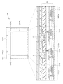
図3Aおよび図3Bは、画素部110Aと回路部110Bとのレイアウトを説明するための模式図であり、図3AがXY平面構成、図3Bが断面構成を表している。なお、図3Bは、図3AのI−I線における矢視断面図である。
FIGS. 3A and 3B are schematic diagrams for explaining the layout of the
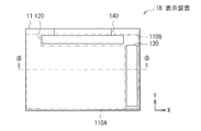
画素部110Aは、基板11のほぼ全面にわたって形成されている。つまり、表示装置1では、表示パネルの一面のほぼ全域が有効表示領域となっており、パネルの端面e1付近まで発光可能となっている。回路部110Bは、画素部110Aの周辺領域ではなく、画素部110Aと対向するように設けられている。具体的には、表示装置1では、回路部110Bを含む層(第1層F1)と、画素部110Aを含む層(第2層F2)とが、積層されている。ここでは、駆動側基板11上に、第1層F1と、第2層F2とが、この順に形成されている。第2層F2上には、封止基板12が設けられる。なお、回路部110Bの走査線駆動回路120と信号線駆動回路130とは、図示しない配線を通じて外部接続用のパッド部140に電気的に接続されている。
The pixel portion 110 </ b> A is formed over substantially the entire surface of the
第1層F1は、回路部110Bの構成要素(シフトレジスタ回路、バッファ回路およびロジック回路などの回路要素)を含む層である。本実施の形態では、回路部110Bの回路要素が、第1層F1内の選択的な領域に偏って(密に)形成されている。具体的には、画素部110A(表示領域A)のXY平面形状が矩形状であり、この矩形状の3辺に対応する領域に、回路部110Bが形成されている。換言すると、表示装置1は、表示領域Aの矩形状の3辺に対応して、画素部110Aと回路部110Bとが積層する部分(積層部B1)を有している。
The first layer F1 is a layer including components (circuit elements such as a shift register circuit, a buffer circuit, and a logic circuit) of the
第2層F2は、画素部110Aの構成要素(例えば、有機EL素子10、書き込みトランジスタWSTr、駆動トランジスタDRTr、キャパシタCs等)を含む層である。但し、詳細は後述するが、画素部110Aの全ての構成要素が第2層F2に形成される必要はなく、一部の構成要素が第1層F1に形成されていてもよい。
The second layer F2 is a layer including components of the
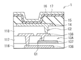
図4は、表示装置1の詳細な断面構成を表したものである。なお、図4では、R,G,B,Wの4画素に対応する領域のみを示している。また、スケール、画素数、積層部B1の位置等についても実際のものとは異なっている。表示装置1は、例えばトップエミッション方式(上面発光方式)の有機電界発光装置であり、上述のように、駆動側基板11と封止基板12との間に、回路部110Bを含む第1層F1と、画素部110Aを含む第2層F2と備えたものである。以下、各構成要素について説明する。
FIG. 4 shows a detailed cross-sectional configuration of the
駆動側基板11は、例えばガラスなどの基板から構成されている。但し、駆動側基板11は、ガラスに限定されるものではなく、この他にも、例えば石英あるいは樹脂などから構成されていてもよい。封止基板12は、ガラスなどの透明基板から構成されている。トップエミッション方式の場合には、封止基板12が透明性を有していればよく、駆動側基板11は透明性を持たない材料から構成されていても構わない。
The driving
(第1層F1)
第1層F1は、回路部110Bとして複数の回路要素を含み、積層部B1には、各種素子(トランジスタおよび容量素子など)が形成される。但し、図4には、一例としてトランジスタ13Bのみを図示している。トランジスタ13Bは、駆動側基板11上に、ゲート電極131と、半導体層132と、電極層133とを有している。ゲート電極131と半導体層132の間には、ゲート絶縁膜111が、半導体層132と電極層133との間には、層間絶縁膜112が、それぞれ形成されている。電極層133上には層間絶縁膜113が形成されている。なお、本実施の形態では、第1層F1内の積層部B1以外の領域(図3A中の領域110C)には、電源線配線などの配線層134が配置されている。
(First layer F1)
The first layer F1 includes a plurality of circuit elements as the
ゲート電極131は、例えばモリブデン(Mo)から構成されている。半導体層132は、例えば低温ポリシリコン(LTPS:Low Temperature Poly-silicon)から構成されている。電極層133は、例えばソースまたはドレインとして機能する電極、信号線用配線あるいは電源線用配線である。この電極層133は、例えばチタン(Ti)およびアルミニウム(Al)を積層させた多層膜(Ti/AlあるいはTi/Al/Ti)である。なお、図4において、トランジスタ「13A」,「13B」として図示した部分は、厳密にはトランジスタ構造となっていないが、説明上そのように記載している。図示した部分は、詳細には、トランジスタ13A,13Bがそれぞれ形成される層構造に相当する。また、以降の断面図においても同様である。
The
ゲート絶縁膜111、層間絶縁膜112,113は、シリコン酸化膜、シリコン窒化膜、シリコン酸窒化膜および酸化アルミニウム膜などの無機膜からなり、それらのうちの1つからなる単層膜であってもよいし、2つ以上からなる積層膜であってもよい。
The
層間絶縁膜113上には、平坦化膜114が形成されている。平坦化膜114は、例えばアクリル樹脂などの有機膜により構成されている。この平坦化膜114上には、シールド層135が設けられている。
A
シールド層135は、例えばチタンおよびアルミニウムの積層膜(Ti/Al/Ti)、あるいはITOなどにより構成されている。シールド層135は、第2層F2の形成過程で使用されるレーザ光の影響が第1層F1に及ばないようにするためのレーザ光遮蔽機能を有するものである。シールド層135の形成領域は、特に限定されないが、第1層F1と第2層F2との層間接続部分(コンタクト部分)を除いた、駆動側基板11のほぼ全面に形成されている。このシールド層135を覆って、層間絶縁膜115が形成されており、層間絶縁膜115上に、第2層F2が形成される。つまり、第2層F2は、第1層F1上に、平坦化膜114、シールド層135および層間絶縁膜115を介して形成されている。ただし、このシールド層135は必ずしも設けられていなくともよい。
The
(第2層F2)
第2層F2は、画素部110Aとして複数の画素PXLCを含み、第1層F1の全域にわたって、上述した構成要素(有機EL素子10,キャパシタCs,書き込みトランジスタWSTr,駆動トランジスタDRTr)が形成されている。但し、図4には、画素PXLCの一部の構成要素であるトランジスタ13A(上記の駆動トランジスタDRTrに相当)と、有機EL素子10のみを図示している。
(Second layer F2)
The second layer F2 includes a plurality of pixels PXLC as the
トランジスタ13Aは、層間絶縁膜115上に、ゲート電極136と、半導体層137と、ソース・ドレイン電極138とを有している。ゲート電極136と半導体層137の間には、ゲート絶縁膜116が、半導体層137とソース・ドレイン電極138との間には、層間絶縁膜117が、それぞれ形成されている。ソース・ドレイン電極138上には平坦化膜118が形成されている。このトランジスタ13Aは、第1層F1に形成されたトランジスタ13Bと平面視的に重畳して形成されている。
The
ゲート電極136は、例えばモリブデン(Mo)から構成されている。半導体層137は、例えば低温ポリシリコン(LTPS)から構成されている。ソース・ドレイン電極138は、ソースまたはドレインとして機能する電極であり、上記電極層133と同様の材料から構成されている。なお、キャパシタCsは、図4には図示しないが、ゲート電極136、ゲート絶縁膜116および半導体層137の層構造を利用して形成されている。ゲート絶縁膜116、層間絶縁膜117は、シリコン酸化膜、シリコン窒化膜、シリコン酸窒化膜および酸化アルミニウム膜などの無機膜からなり、それらのうちの1つからなる単層膜であってもよいし、2つ以上からなる積層膜であってもよい。このように、本実施の形態では、積層部B1に形成されるトランジスタ13Aとトランジスタ13Bとが、いずれもLTPSを含んでいる(半導体層132,137がLTPSから構成されている)。このため、トランジスタ13Aを形成する際のレーザ照射によって、トランジスタ13Bの特性への影響が懸念されるが、上記のように第1層F1と第2層F2との間にシールド層135が設けられていることから、トランジスタ13Bへのレーザ光の影響は軽減される。但し、シールド層135は必ずしも設けられていなくともよく、この場合には、レーザ照射条件を適切に設定することにより、所望の特性を有するトランジスタ13A,13Bを形成可能である。
The
なお、第1層F1と第2層F2とにおいて、互いに異なる材料を用いてトランジスタ13A,13Bを形成することも可能である。例えば、第1層F1のトランジスタ13BがLTPSを含み、第2層F2のトランジスタ13Aが透明酸化物半導体(TOS:Transparent Oxide Semiconductor)を含んでいてもよい。換言すると、半導体層132がLTPSから構成され、半導体層137が透明酸化物半導体から構成されていてもよい。この場合、トランジスタ13Aの形成時に、トランジスタ13Bの特性が影響を受けにくいことから、トランジスタ13A,13Bの各特性を制御し易い。また、第2層F2の形成時にレーザ照射工程が不要となることから、第1層F1へのダメージコントロールが不要となる。また、第1層F1については、CMOS(Complementary Metal-Oxide Semiconductor)構造により回路部を形成可能となる。
It is also possible to form the
あるいは、第1層F1のトランジスタ13Bと、第2層F2のトランジスタ13AとのいずれもがTOSを含んでいてもよい(半導体層132,137がTOSから構成されていてもよい)。あるいは更に、第1層F1のトランジスタ13BがTOSを含み、第2層F2のトランジスタ13AがLTPSを含んでいてもよい(半導体層132がTOSから構成され、半導体層137がLTPSから構成されていてもよい)。なお、これらのLTPSおよびTOSに限られず、他の半導体、例えばアモルファスシリコン、微結晶シリコンあるいは高温ポリシリコン(HTPS:High Temperature Poly-silicon)が用いられてもよい。
Alternatively, both of the
平坦化膜118は、例えばアクリル樹脂などの有機膜により構成されている。この平坦化膜118上に、画素PXLC毎に、有機EL素子10が形成されている。
The
有機EL素子10は、駆動側基板11の側から順に、第1電極14と、有機層16と、第2電極17とを有するものである。第1電極14は、画素毎に設けられており、この第1電極14上には全画素にわたって画素間絶縁膜15が形成されている。画素間絶縁膜15は、第1電極14に対向して開口H1を有している。この開口H1内において、第1電極14と有機層16とが接している。第2電極17は、例えば、有機層16を覆うように、全画素にわたって形成されている。第2電極17上には、保護膜および封止樹脂を含む樹脂層18を介して、封止基板12が貼り合わせられている。封止基板12の一面(有機EL素子10に対向する面)には、BM/CF層19が形成されている。有機EL素子10は白色発光素子であり、有機EL素子10から発せられた白色光が、BM/CF層19を通過することによりR,G,B,Wのいずれかの色光(LR,LG,LB,LW)に分離されて取り出される。
The
第1電極14は、光反射性を有する反射電極である。第1電極14は、アノードとして機能する場合には、例えばアルミニウム(Al),白金(Pt),金(Au),銀(Ag),クロム(Cr),タングステン(W),ニッケル(Ni),銅(Cu),鉄(Fe),コバルト(Co),タンタル(Ta)などの金属の単体あるいはそれらのうちの少なくとも1種を含む合金から構成されることが望ましい。合金としては、例えばAg−Pd−Cu合金(銀とパラジウムと銅の合金)、あるいはAl−Nd合金を挙げることができる。あるいは、第1電極14は、上記のような金属よりなる膜と、透明導電膜との積層膜であってもよい。第1電極14は、正孔注入性の高い材料により構成されていることが望ましいが、そうでない材料(アルミニウム(Al)あるいはアルミニウムを含む合金等)であっても、適切な正孔注入層を設けることによってアノードとして使用することができる。透明導電膜としては、例えばインジウムとスズの酸化物(ITO)、InZnO(インジウ亜鉛オキシド)、および酸化亜鉛(ZnO)とアルミニウム(Al)との合金などが挙げられる。
The
画素間絶縁膜15は、画素開口(発光領域,発光開口)を定義(区画)すると共に、第1電極14同士を電気的に分離するためのものである。この画素間絶縁膜15は、例えばアクリル樹脂あるいはポリイミドなどの有機材料から構成されている。
The inter-pixel
有機層16は、電界をかけることにより電子と正孔との再結合が起こり、色光を発生する有機電界発光層を含むものである。ここでは、有機層16は、例えば白色光を発生する白色発光層を含み、例えば全画素にわたって形成されている。白色発光層は、例えば赤色発光層、緑色発光層および青色発光層を積層した構造、あるいは青色発光層と黄色発光層とを積層した構造を有している。但し、有機層16の構成はこれに限定されず、画素毎に発光層が塗り分けられていてもよい。具体的には、画素PXLC毎に、赤色発光層,緑色発光層,青色発光層および白色発光層のうちのいずれかが形成されていてもよい。また、有機層16は、そのような有機電界発光層の他にも、例えば正孔注入層、正孔輸送層および電子輸送層を含んでいてもよい。また、有機層16と第2電極17との間には、電子注入層等が形成されていてもよい。
The
第2電極17は、適度な仕事関数をもつと共に、光透過性を有する導電性材料、例えばITO(酸化インジウム錫)あるいはIZO(酸化インジウム亜鉛)などの透明導電膜から構成されている。また、第2電極17の構成材料としては、この他にも、マグネシウムと銀との合金(MgAg合金)が挙げられる。
The
樹脂層18は、例えばシリコン窒化膜などの無機膜から構成される保護膜と、例えばエポキシ樹脂などから構成される封止樹脂とを含んでいる。
The
BM/CF層19は、第2電極17の光出射側に、全画素にわたって形成されている。このBM/CF層19は、例えばXY平面形状が格子状である遮光部分(ブラックマトリクス)と、格子状の開口部分に形成されたカラーフィルタ(赤色フィルタ19R,緑色フィルタ19G,青色フィルタ19B)とを含む層である。赤色フィルタ19R,緑色フィルタ19G,青色フィルタ19Bは、それぞれ有機EL素子10に対向して形成されている。赤色フィルタ層19Rは、赤色光を選択的に透過させ、その他の波長を吸収するものであり、緑色フィルタ層19Gは、緑色光を選択的に透過させ、その他の波長を吸収するものであり、青色フィルタ層19Bは、青色光を選択的に透過させ、その他の波長を吸収するものである。なお、W画素では、カラーフィルタが設けられておらず、有機層16から発せられた白色光がそのまま封止基板12上へ取り出される。あるいは、W画素には、輝度や色度を調整する目的で光学フィルタが設けられていてもよい。このBM/CF層19の表面(有機EL素子10側の面)は、オーバーコート層119によって覆われている。
The BM /
[作用,効果]
本実施の形態の表示装置1では、第1電極14と第2電極17とを介して有機層16に駆動電流が供給されると、有機電界発光素子10において色光(例えば白色光)が発生する。この白色光が、第2電極17、樹脂層18、BM/CF層19および封止基板12を透過することにより、光LR,LG,LB,LWとして上方へ出射される。このようにして画像表示がなされる。
[Action, effect]
In the
ここで、一般的な有機ELディスプレイは、パネルの有効表示領域の周辺に額縁と呼ばれる非表示領域を有している。この額縁に、駆動回路が配置されている。 Here, a general organic EL display has a non-display area called a frame around the effective display area of the panel. The drive circuit is disposed in this frame.
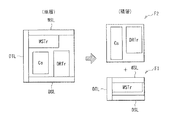
図5に、本実施の形態の比較例(比較例1)に係る表示装置(表示装置100)の平面構成(上図)および断面構成(下図)について示す。表示装置100は、駆動側基板1011上に、複数の画素(画素回路)を含む画素部1010Aを有する。この画素部1010Aの周辺に、走査線駆動回路1012と信号線駆動回路1013とを含む回路部1010Bが形成されている。つまり、比較例1では、画素部1010Aと、回路部1010Bとが、互いに同じ層F0内に形成されている。詳細には、画素部1010Aの構成要素であるトランジスタ101Aと、回路部1010Bの構成要素であるトランジスタ101Bとが、駆動側基板1011の面内方向に沿って並列に形成されている。これらのトランジスタ101Aとトランジスタ101Bとは、互いに同じ工程でパターン形成されるものである。
FIG. 5 shows a plan configuration (upper view) and a cross-sectional configuration (lower view) of a display apparatus (display apparatus 100) according to a comparative example (comparative example 1) of the present embodiment. The
この比較例1の表示装置100では、上記のように画素部1010Aの周辺に回路部1010Bが形成される。回路部1010Bの配置スペースとして額縁を確保することが望ましい。特に中小型のディスプレイでは、回路部1010Bの占有面積を減らすことが難しく、狭額縁化が困難である。
In the
これに対し、本実施の形態の表示装置1では、画素部110Aの周辺に回路部110Bが形成されるのではなく、回路部110Bを含む第1層F1と、画素部110Aを含む第2層F2とが積層されている。具体的には、駆動側基板11上に、第1層F1と第2層F2とがこの順に形成されている。
On the other hand, in the
このような構成により、画素部110Aの周辺に、回路部110Bを配置するためのスペースを確保する必要がなくなる。即ち、画素部110Aの周辺領域における回路部110Bの配置スペースが削減される。
With such a configuration, it is not necessary to secure a space for arranging the
また、画素部110Aの矩形状の3辺に対応する領域に、画素部110Aと回路部110Bとが重畳する積層部B1を有している。これにより、第1層F1のうちの、回路部110Bが形成されていない領域110C(積層部B1以外の領域)には、例えば配線層134を形成することができる。このため、配線レイアウトの自由度が向上する。加えて、配線層134の線幅を十分に大きく確保することができることから、配線層134を所望のインピーダンスで形成可能となる。また、領域110Cには、このような配線層134の他にも、センサ素子やエレクトロクロミック素子などの機能素子を配置することが可能である。これにより、例えばタッチセンサ機能付きのディスプレイや、透明モードと不透明モードとを切り替えることが可能なディスプレイ(後述)などを実現可能となる。このように、回路部110Bが第1層F1内において偏って配置される場合、第1層F1にはスペース(領域110C)が生じ、このスペースを様々な用途で活用することができる。
Further, a stacked portion B1 in which the
以上のように本実施の形態では、2次元配置された複数の画素PXLCを有する画素部110Aと、複数の画素PXLCを表示駆動する回路部110Bとを備え、回路部110Bを含む第1層F1と、画素部110Aを含む第2層F2とが積層されている。これにより、画素部110Aの周辺領域における回路部110Bの配置スペースを削減することができる。よって、狭額縁あるいは額縁レスを実現することが可能となる。
As described above, in the present embodiment, the first layer F1 including the
次に、上記第1の実施の形態の他の実施の形態および変形例について説明する。なお、上記第1の実施の形態と同様の構成要素については同一の符号を付し、適宜その説明を省略する。 Next, other embodiments and modified examples of the first embodiment will be described. The same components as those in the first embodiment are given the same reference numerals, and the description thereof will be omitted as appropriate.
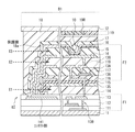
<変形例1>
図6は、上記第1の実施の形態の変形例(変形例1)に係る表示装置(表示装置1A)の画素部110Aと回路部110Bとのレイアウトを説明するための平面模式図である。図7は、図6のIA−IA線における矢視断面図である。上記第1の実施の形態では、回路部110Bが第1層F1において、選択的な領域(矩形状の3辺に対応する領域)に偏って配置される場合について説明したが、回路部110Bのレイアウトはこれに限定されない。例えば、本変形例のように、回路部110Bを構成する複数の回路要素が第1層F1内に分散して配置されていてもよい。換言すると、第1層F1の全域にわたって回路部110Bが形成され、表示領域Aの全域が、画素部110Aと回路部110Bとが積層される積層部B2となっている。
<
FIG. 6 is a schematic plan view for illustrating the layout of the
図8A〜図8Cは、回路部110Bの回路要素(回路要素D1,D2,D3)のレイアウトの一例を模式的に表したものである。図8Aに示したように、上記第1の実施の形態のように所定の領域にのみ回路部110Bが配置される場合、例えば、走査線駆動回路130の回路要素D1〜D3は、所定の領域内に収まるように隙間なく密に配置される。一方、本変形例のように、積層部B2が表示領域Aの全域に形成される場合には、例えば図8Bに示したように、回路要素D1〜D3をそれぞれ細分化し、間隙Saをおいて配置させることができる。あるいは、図8Cに示したように、回路要素D1〜D3をX方向に沿って延在する細長い領域にわたって配置することもできる。走査線駆動回路130は、一般的に画素部110Aの1辺に対応する領域にY方向に沿って延在するように形成されるが、本変形例では、回路部110Bのレイアウトの制限が小さいことから、X方向に沿って延在するように形成することもできる。また、このようなX方向に伸びる回路要素D1〜D3を複数本配列させることも可能である。
8A to 8C schematically illustrate an example of the layout of circuit elements (circuit elements D1, D2, and D3) of the
このように、第1層F1に回路部110Bの回路要素を分散して配置してもよく、これにより、回路部110Bのレイアウトの自由度が高まる。また、回路部110Bの分散配置により、回路要素の密度が低くなることから、空いた領域に透過窓を形成して表示領域Aの透明性を高めることもできる(詳細は後述)。なお、上記の回路部110Bのレイアウトは一例であり、用途や他の素子のレイアウトに応じて様々なレイアウトを取りうる。
As described above, the circuit elements of the
<変形例2>
図9は、上記第1の実施の形態の変形例(変形例2)に係る表示装置(表示装置1B)の画素部110Aと回路部110Bとのレイアウトを説明するための平面模式図である。図10は、図9のIB−IB線における矢視断面図である。上記第1の実施の形態では、回路部110Bが第1層F1において、選択的な領域(矩形状の3辺に対応する領域)に偏って配置される場合について説明したが、回路部110Bのレイアウトはこれに限定されない。例えば、本変形例のように、回路部110Bを構成する複数の回路要素が第1層F1において、矩形状の2辺に対応する領域に配置されていてもよい。具体的には、回路部110Bのうち走査線駆動回路130が、矩形状の1辺に集約して設けられている。この場合にも、第1層F1のうち、画素部110Aと回路部110Bとの積層部B1以外の領域110Cには、上記第1の実施の形態と同様、配線層134を形成することができる。その一例を、図11に示す。あるいは、領域110Cには、上述したような機能素子が形成されていてもよい。
<
FIG. 9 is a schematic plan view for illustrating the layout of the
このように、走査線駆動回路130を矩形状の1辺(信号線駆動回路120とは異なる1つの辺)に対応する領域に集約して形成することにより、即ち回路部分を矩形状の2辺に集約して形成することにより、後述の透明ディスプレイ用途において、次のような効果がある。詳細は後述するが、回路部分が集約されていない2辺に対応する領域の第2層F2の画素部110Aに透過窓を設けることで、額縁レスの2辺透明ディスプレイを実現できる。また、信号線駆動回路120と走査線駆動回路130とを、矩形状の1辺に集約して配置するようにしてもよく、この場合には、額縁レスの3辺透明ディスプレイを実現可能となる。
As described above, by collectively forming the scanning
<第2の実施の形態>
上記第1の実施の形態において説明したように、画素部110Aと回路部110Bとの積層(第1層F1と第2層F2との積層)により、第1層F1におけるレイアウトの自由度が高まり、回路部110Bを分散して配置することが可能となる。このような回路部110Bの分散配置を利用して、例えば、光透過性を有し、背面側の景色が透けて見えるような透明ディスプレイを実現可能となる。
Second Embodiment
As described in the first embodiment, the degree of freedom in the layout in the first layer F1 is increased by the lamination of the
ここで、一般的なディスプレイでは、図12に示したように、例えば4色の画素10R,10G,10B,10Wのそれぞれに発光部(発光開口)E1が形成され、この発光部E1からのみ光が出射するように構成されている。これに対し、図13に示したように、透明ディスプレイでは、画素10R,10G,10B,10Wのそれぞれに、発光部E1と、光透過用の窓(透過部T1)とが形成されている。この透過部T1により、各画素を光が透過可能となり、透明性を有するディスプレイを実現可能となる。
Here, in a general display, as shown in FIG. 12, for example, a light emitting portion (light emitting aperture) E1 is formed in each of the four
図14は、本開示の第2の実施の形態の表示装置(表示装置2)の要部構成を表すXY平面図である。図14において、上図は、画素部110Aを含む第2層F2の要部構成を、下図は、回路部110Bを含む第1層F1の要部構成を、それぞれ表す。このように、本実施の形態では、第2層F2において、有機EL素子10毎(画素PXLC毎)に、発光部E1と透過部T1とが設けられている。一方、第1層F1にも、透過部T2が設けられている。上記変形例1と同様、第1層F1では、回路部110Bの回路要素D1〜D3が分散配置され、これによって生じた間隙に透過部T2が形成されている。第1層F1における透過部T2と第2層F2における透過部T1とは、積層方向において互いに連通する位置に設けられ、これらの透過部T1,T2を貫通して光が透過する。なお、第1層F1では、回路要素D1,D2,D3をそれぞれ電気的に接続する配線層139が、透過部T2を避けるように配置されている。
FIG. 14 is an XY plan view showing the main configuration of a display device (display device 2) according to the second embodiment of the present disclosure. In FIG. 14, the upper diagram shows the main configuration of the second layer F2 including the
図15は、表示装置2の具体的な断面構成を表したものである。このように、第1層F1に回路部110Bの回路要素が分散配置されており(ここではトランジスタ13Bのみを図示する)、積層方向において連通する透過部T1,T2を光が透過する。なお、本実施の形態では、ブラックマトリクスは形成されておらず、樹脂層18上には、赤色フィルタ21R,緑色フィルタ21G,青色フィルタ21Bを含むCF層21が形成されている。CF層21の表面は、オーバーコート層119によって覆われている。
FIG. 15 shows a specific cross-sectional configuration of the
図16は、発光部E1および透過部T1,T2付近の素子構造を拡大したものである。このように、発光部E1に対応する領域では、トランジスタ13A,13Bが重畳すると共に、有機EL素子10が形成されている。金属などの不透明な層は、透過部T1,T2を避けて設けられている。一方、透過部T1,T2に対応する領域では、比較的透明性の高い膜が積層されている。材料や厚みに起因して透明性が低い層(例えば、ここでは平坦化膜118、画素間絶縁膜15)では、開口(開口H2)を設けることにより、あるいは厚みを薄くすることによって光透過性が高められている。なお、図16において、トランジスタ「13A」,「13B」として図示した部分は、厳密にはトランジスタ構造となっていないが、説明上そのように付記している。図示した部分は、トランジスタ13A,13Bがそれぞれ形成される層構造に相当する。
FIG. 16 is an enlarged view of the element structure in the vicinity of the light emitting portion E1 and the transmitting portions T1 and T2. As described above, in the region corresponding to the light emitting unit E1, the
本実施の形態の表示装置2においても、回路部110Bを含む第1層F1と、画素部110Aを含む第2層F2とが積層されることにより、画素部110Aの周辺領域における回路部110Bの配置スペースを削減することができる。よって、上記第1の実施の形態と同等の効果を得ることができる。また、第1層F1内に回路部110Bを分散して配置することにより、第1層F1と第2層F2とにおいて連通する透過部T1,T2を形成することができ、透明ディスプレイを実現可能となる。
Also in the
また、上記変形例2において述べたように走査線駆動回路130を矩形状の1辺(信号線駆動回路120とは異なる1つの辺)に対応する領域に集約し、即ち回路部分を矩形状の2辺に集約して形成する。その上で、他の2辺に対応する領域の第2層F2の画素部110Aに透過窓を設けることで、図17Aに示したように、回路部110Bが形成されていない2辺に対応する領域を透明にし、かつ端面発光とすることができる。つまり、回路部110Bの集約されている2辺を除いた領域が透明領域(透明領域110D)となり、額縁レスの2辺透明ディスプレイを実現可能となる。また、信号線駆動回路120と走査線駆動回路130とを、矩形状の1辺に集約して配置するようにしてもよく、この場合には、額縁レスの3辺透明ディスプレイを実現可能となる(図17B)。但し、この場合、走査線WSLは、信号線DTLと同様にY方向に沿って延伸して形成される。この走査線WSLは、他の層にX方向に沿って形成された配線とクロスする位置で層間接続される。
Further, as described in the second modification, the scanning
<変形例3>
図18は、上記第1,第2の実施の形態の変形例(変形例3)に係る表示装置(表示装置2A)の断面構成を表したものである。上記実施の形態等では、トップエミッション方式の有機EL素子10を用いた表示装置を例に挙げて説明したが、本変形例のように、ボトムエミッション方式(下面発光方式)の有機EL素子(有機EL素子20)が用いられてもよい。本変形例の表示装置2Aでは、第1層F1において、上記変形例1および第2の実施の形態と同様、回路部110Bが分散配置され、回路要素同士の間隙を光(発光光、あるいは発光光および透過光)が通るように構成される。有機EL素子20は、第1電極22と第2電極23との間に有機層16を有している。有機EL素子20(発光部E2)が、トランジスタ13A,13Bに非重畳となるように形成されている。第1電極22は、ITOなどの透明導電膜により構成され、画素間絶縁膜15によって画素毎に電気的に分離されている。第2電極23は、反射電極であり、例えば上記第1の実施の形態の第1電極14と同様の材料により構成されている。カラーフィルタ(赤色フィルタ24R,緑色フィルタ24G,青色フィルタ24B)は、第1電極22よりも下層に形成され、いわゆるオンチップカラーフィルタ(OCCF)となっている。
<
FIG. 18 illustrates a cross-sectional configuration of a display device (display device 2A) according to a modification (modification 3) of the first and second embodiments. In the above embodiments and the like, the display device using the top emission type
このように、第1層F1と第2層F2との積層構造において、第1層F1内に回路部110Bを分散配置することにより、ボトムエミッション方式のディスプレイ、あるいはボトムエミッション方式の透明ディスプレイを実現可能となる。表示装置2Aにおいても、狭額縁あるいは額縁レスを実現可能となる。
As described above, in the laminated structure of the first layer F1 and the second layer F2, the bottom emission type display or the bottom emission type transparent display is realized by dispersing the
<第3の実施の形態>
図19は、本開示の第3の実施の形態の表示装置(表示装置3)の断面構成を表したものである。本実施の形態においても、上記第1の実施の形態と同様、回路部110Bを含む第1層F1と、画素部110Aを含む第2層F2とが積層されている。また、回路部110Bと画素部110Aとは、積層部B1において重畳する。但し、本実施の形態では、上記第1の実施の形態と異なり、画素PXLCのうちの一部が、第2層F2ではなく第1層F1に形成されている。例えば、書き込みトランジスタWsTrに相当するトランジスタ13Cが第1層F1に形成されている。第2層F2には、駆動トランジスタDRTrに相当するトランジスタ13Aが、トランジスタ13Cに平面視的に重畳するように形成されている。トランジスタ13Aとトランジスタ13Cとは、平坦化膜114等を介して層間接続されている。
Third Embodiment
FIG. 19 illustrates a cross-sectional configuration of a display device (display device 3) according to a third embodiment of the present disclosure. Also in the present embodiment, as in the first embodiment, the first layer F1 including the
図20は、画素PXLCの構成要素(書き込みトランジスタWSTr,駆動トランジスタDRTr,キャパシタCs)を1つの層に配置(以下、「単層配置」という)した場合と、2層(第1層F1と第2層F2)に分けて配置(以下、「積層配置」という)した場合とレイアウトの一例を表したものである。なお、信号線DTL,走査線WSLおよび電源線DSLについても図示している。このように、単層配置の場合には、書き込みトランジスタWSTr,駆動トランジスタDRTr,キャパシタCsが互いに重畳しないように配置される。一方、積層配置の場合には、例えば第1層F1に、書き込みトランジスタWSTrと、信号線DTL,走査線WSLおよび電源線DSLとが配置され、第2層F2に、駆動トランジスタDRTrとキャパシタCsとが配置される。このように、積層配置では、第1層F1および第2層f2のそれぞれにおける素子の占有面積が、単層配置の場合よりも減少する。 FIG. 20 shows the case where the components of the pixel PXLC (write transistor WSTr, drive transistor DRTr, capacitor Cs) are arranged in one layer (hereinafter referred to as “single-layer arrangement”), and two layers (first layer F1 and It shows an example of a case where it is divided into two layers F2) and arranged (hereinafter referred to as "stacked arrangement") and an example of layout. The signal line DTL, the scanning line WSL, and the power supply line DSL are also illustrated. As described above, in the case of the single layer arrangement, the write transistor WSTr, the drive transistor DRTr, and the capacitor Cs are arranged so as not to overlap with each other. On the other hand, in the case of the stacked arrangement, for example, the write transistor WSTr, the signal line DTL, the scan line WSL, and the power supply line DSL are disposed in the first layer F1, and the drive transistor DRTr and the capacitor Cs are disposed in the second layer F2. Is placed. Thus, in the stacked arrangement, the occupied area of the element in each of the first layer F1 and the second layer f2 is smaller than in the single layer arrangement.
図21は、上記のような積層配置と、回路要素の分散配置とを組み合わせてレイアウトを行った例である。なお、領域Pは、1つの画素に相当する領域である。このように、第1層F1では、書き込みトランジスタWSTrと、信号線DTL,走査線WSLおよび電源線DSLと共に、回路要素D1,D2,…が配置されている。換言すると、第1層F1では、回路要素の分散配置によって、空きスペースができることから、その空きスペースを利用して、書き込みトランジスタWSTr等が配置される。 FIG. 21 shows an example in which a layout is performed by combining the above-described stacked arrangement and the distributed arrangement of circuit elements. The area P is an area corresponding to one pixel. As described above, in the first layer F1, the circuit elements D1, D2,... Are arranged together with the write transistor WSTr, the signal line DTL, the scanning line WSL, and the power supply line DSL. In other words, in the first layer F <b> 1, since free space is made by the distributed arrangement of the circuit elements, the write transistor WSTr or the like is arranged using the free space.
本実施の形態では、上記第1の実施の形態と同様、回路部110Bを含む第1層F1と、画素部110Aを含む第2層F2とが積層されることにより、画素部110Aの周辺領域における回路部110Bの配置スペースを削減することができる。よって、上記第1の実施の形態と同等の効果を得ることができる。また、画素部110Aの一部を第1層F1に形成することにより、図22の単層配置の場合と同じ構成要素を、図23に示したように、第1層F1(書き込みトランジスタWSTr,信号線DTL,走査線WSLおよび電源線DSL)と、第2層F2(駆動トランジスタDRTr,キャパシタCs)とにそれぞれ形成することができる。つまり、書き込みトランジスタWSTr,信号線DTL,走査線WSLおよび電源線DSLと、駆動トランジスタDRTr,キャパシタCsとを、平面視的に重畳して配置することができる。このため、画素幅p12が、単層配置の場合の画素幅p11よりも小さくなり、高精細化を実現可能となる。
In the present embodiment, as in the first embodiment, the first layer F1 including the
また、上記のような積層配置では、トランジスタ13A(駆動トランジスタDRTr)とトランジスタ13C(書き込みトランジスタWSTr)とが、それぞれ独立したプロセスにより形成される。このため、トランジスタ13Aとトランジスタ13Cとの性能を個別に制御することが可能である。
Further, in the above-described stacked arrangement, the
例えば、第2層F2のトランジスタ13A(駆動トランジスタDRTr)では、第1層F1のトランジスタ13C(書き込みトランジスタWSTr)に比べ、高い性能(例えば、高移動度)が要求されない。このため、例えば、図24Aに示したように、トランジスタ13Aでは、ゲート電極1301とチャネル層1303との間のゲート絶縁膜1303aの厚みを比較的大きく設定する。一方、図24Bに示したように、トランジスタ13Cでは、ゲート電極1301とチャネル層1303との間のゲート絶縁膜1303bの厚みを比較的小さく設定する。このようにトランジスタ13A,13Cの性能を個別に制御することができる。
For example, the
また、第1層F1には、同一のパターニング工程により、トランジスタ13Cを含む複数のトランジスタが形成されてもよい。例えば、図24Cに示したように、ゲート絶縁膜1302cを間にしてゲート電極1301aとチャネル層1303aが配置されたトランジスタと、ゲート絶縁膜1302dを間にしてゲート電極1301bとチャネル層1303bが配置されたトランジスタとが形成されてもよい。あるいは、図24Dに示したように、ゲート絶縁膜1302cを間にしてゲート電極1301aとチャネル層1303aが配置されたトランジスタと、ゲート絶縁膜1302c,1302dを間にしてゲート電極1301bとチャネル層1303bが配置されたトランジスタとが形成されてもよい。なお、上述したように、上下のトランジスタにおいて、構成材料(LTPS,TOS,アモルファスシリコン,微結晶シリコン,HTPS等)を変えることによっても性能に変化を持たせることができる。このように、積層配置によって、様々な性能のトランジスタを組み合わせて使用することができる。
Further, in the first layer F1, a plurality of transistors including the
<変形例4>
図25は、上記第3の実施の形態の変形例(変形例4)に係る表示装置(表示装置3A)の断面構成を表したものである。本変形例では、画素部110Aにおいて、有機EL素子10の第1電極(第1電極14A)が、駆動トランジスタDRTrに相当するトランジスタ(トランジスタ13A1)のソース・ドレイン電極を兼ねている。換言すると、第1電極14Aとトランジスタ13A1との間の接続層(図4に示したソース・ドレイン電極138に相当)が省略されており、上記第1の実施の形態よりも簡易な層構造となっている。詳細には、本変形例では、上記第1の実施の形態における層間絶縁膜117とソース・ドレイン電極138とが省略され、半導体層137に第1電極14Aが直接に接続されることで、プロセス工程数が削減される。この理由について、以下に説明する。
<Modification 4>
FIG. 25 shows a cross-sectional configuration of a display device (
図26は、本変形例の比較例(比較例2)として上記第1の実施の形態に係る表示装置1の要部断面構成を表したものである。図27は、表示装置1の要部構成の平面レイアウトを表したものである。第2層F2に、画素PXLCの構成要素(書き込みトランジスタWSTr,駆動トランジスタDRTr,キャパシタCs等)が形成される場合、例えば図27に示したようなレイアウトで配置される。即ち、ゲート電極136と同一層内に金属層(Mo層)S1がパターン形成され、半導体層137と同一層内には、半導体層(p−Si層)S2がパターン形成されている。これらの金属層S1および半導体層S2は、ソース・ドレイン電極138と同一層内にパターン形成される金属層(Ti/Al層)S3と、コンタクト部C1等を介して層間接続されている。金属層S3には、走査線WSLや電源線DSLなどの配線層も形成される。このため、比較例2では、金属層S3と同一層内に、第1電極14を形成するスペースが乏しいことから、金属層S3とは異なる層に、第1電極14が形成される。具体的には、第1電極14は、平坦化膜118を介して形成されており、第1電極14とソース・ドレイン電極138とが、コンタクト部C2を介して電気的に接続されている。
FIG. 26 illustrates the cross-sectional configuration of the main part of the
ここで、上記第3の実施の形態では、書き込みトランジスタWSTr(トランジスタ13C)が第1層F1に、駆動トランジスタDRTr(トランジスタ13A)が第2層F2に、それぞれ形成された「積層配置」について説明したが、この積層配置によって、第2層F2では、上記比較例2の金属層S3のうち、書き込みトランジスタWSTr,走査線WSLおよび電源線DSLに使用されている部分が不要となる。換言すると、本変形例の表示装置3Aでは、上記金属層S3のうち、駆動トランジスタDRTrに使用されている部分(第1電極14Aを兼ねる部分)のみが配置される。このため、第1電極14Aの面積を比較例2よりも広く確保することができる。
Here, in the third embodiment, the “stacked arrangement” in which the write transistor WSTr (
図28は、表示装置3Aの要部断面構成を表したものである。図29は、表示装置3Aの要部構成の平面レイアウトを表したものである。なお、図29の上図は第2層F2のレイアウト、下図は第1層F1のレイアウトにそれぞれ対応する。本変形例においても、上記第3の実施の形態と同様、第1層F1に、書き込みトランジスタWSTr(トランジスタ13C),走査線WSL,信号線DTLおよび電源線DSLが形成されている。第2層F2には、駆動トランジスタDRTr(トランジスタ13A1)およびキャパシタCsが形成されている。
FIG. 28 shows the cross-sectional configuration of the main part of the
第1層F1では、例えば図29の下図に示したようなレイアウトで、ゲート電極131と同一層内に形成された金属層(Mo層)S1と、半導体層132と同一層内に形成された半導体層(p−Si層)S2と、電極層133と同一層内に形成された金属層(Ti/Al層)S3と、が平面視的に重畳して配置されている。第2層F2では、例えば図29の上図に示したレイアウトで、ゲート電極136と同一層内に形成された金属層(Mo層)S1と、半導体層137と同一層内に形成された半導体層(p−Si層)S2と、第1電極14Aとが、平面視的に重畳して配置されている。
In the first layer F1, for example, the metal layer (Mo layer) S1 formed in the same layer as the
このような積層配置において、コンタクト部C4,C5等を介して第1層F1と第2層F2とが層間接続されている。第2層F2では、コンタクト部C3を介して半導体層137と第1電極14Aが層間接続されている。
In such a stacked arrangement, the first layer F1 and the second layer F2 are connected in layers via the contact portions C4, C5 and the like. In the second layer F2, the
本変形例では、上記のように、積層配置によって第2層F2内に空きスペースが生じることから、第1電極14Aを、金属層S3と同一層内に形成可能となる。よって、層間絶縁膜117およびソース・ドレイン電極138を省略して、第1電極14Aを形成可能となり、層構造およびプロセス工程を簡略化することができる。
In the present modification, as described above, since the vacant space is generated in the second layer F2 due to the stacked arrangement, the
<変形例5>
図30は、上記実施の形態等の変形例(変形例5)に係る表示装置の端面付近の断面構成を表したものである。上記実施の形態等の表示装置は、第1層F1と第2層F2との積層構造を有するが、この積層構造は、本変形例のように、端面e1において無機絶縁膜あるいは金属膜などにより覆われていることが望ましい。具体的には、駆動側基板11上には、第1層F1、平坦化膜114、シールド層135、層間絶縁膜115および第2層F2がこの順に形成されている。第2層F2の上に、樹脂層18およびBM/CF層19を介して封止基板12が貼り合わせられている。
<Modification 5>
FIG. 30 illustrates a cross-sectional configuration in the vicinity of an end face of a display device according to a modification (modification 5) of the above-described embodiment and the like. The display device according to the above-described embodiment and the like has a laminated structure of the first layer F1 and the second layer F2, but this laminated structure is formed of an inorganic insulating film or a metal film on the end face e1 as in this modification. It is desirable to be covered. Specifically, on the driving
この積層構造のうち、特に平坦化膜114と、第2層F2内の平坦化膜118および画素間絶縁膜15とは、有機材料から構成されることが多い。このため、これらの平坦化膜114,118および画素間絶縁膜15を介した水分の浸入が懸念される(X1,X2,X3)。このため、表示装置の端面e1では、平坦化膜114,118および画素間絶縁膜15を覆うように、他の層(無機絶縁膜あるいは金属膜)が延在して形成されていることが望ましい。ここでは、シールド層135、層間絶縁膜115、ゲート電極136(Mo層S1)、層間絶縁膜117、ソース・ドレイン電極138(Ti/Al層S3)、第1電極14および第2電極17が端面e1まで延在形成されている。なお、第2電極17は、駆動側基板11上の第1層F1に形成されたコンタクト部141(カソードコンタクト)に接続されている。また、第2層F2と樹脂層18との間に、表示領域の全面と端面e1とを覆うように保護膜18aが形成されている。保護膜18aは、例えばシリコン酸化膜あるいはシリコン窒化膜などよりなる無機膜である。
In the stacked structure, in particular, the
本変形例のように、端面e1において無機絶縁膜あるいは金属膜よりなる層が、有機膜よりなる層を覆うように形成されることにより、表示装置の封止性能が向上し、信頼性を高めることができる。上記実施の形態等では、第1層F1と第2層F2との積層構造により、層数が増えることから、有機膜による水分の浸入経路が増える可能性があることから、本変形例のような封止構造が有効である。 As in the present modification, the layer formed of the inorganic insulating film or the metal film is formed to cover the layer formed of the organic film at the end face e1, thereby improving the sealing performance of the display device and enhancing the reliability. be able to. In the above embodiment and the like, the number of layers is increased by the stacked structure of the first layer F1 and the second layer F2, and therefore there is a possibility that the water permeation path by the organic film may be increased. Sealing structure is effective.
<適用例>
以下、上記実施の形態等で説明した表示装置の適用例について説明する。上記実施の形態の表示装置は、テレビジョン装置,デジタルカメラ,ノート型パーソナルコンピュータ、携帯電話等の携帯端末装置,ビデオカメラ,スマートフォン,タブレット型ディスプレイなど、外部から入力された映像信号あるいは内部で生成した映像信号を、画像あるいは映像として表示するあらゆる分野の電子機器の表示装置に適用することが可能である。特に、中小型のディスプレイあるいは透明ディスプレイに好適である。以下にその一例を示す。
<Example of application>
Hereinafter, application examples of the display device described in the above-described embodiment and the like will be described. The display device according to the above embodiment is a television device, a digital camera, a laptop personal computer, a portable terminal device such as a mobile phone, a video camera, a smartphone, a tablet display, etc. The present invention can be applied to display devices of electronic devices of all fields that display the resulting video signal as an image or a video. In particular, it is suitable for small to medium sized displays or transparent displays. An example is shown below.
図31Aおよび図31Bは、スマートフォン220の外観を表したものである。このスマートフォン220は、例えば、表側に表示部221および操作部222を有し、裏側にカメラ223を有しており、表示部221に上記実施の形態等の表示装置が搭載されている。
31A and 31B show the appearance of the
図32Aおよび図32Bは、タブレット型ディスプレイ230の外観を表したものである。このタブレット型ディスプレイ230は、例えば、タッチパネル部231、筐体232および操作部233を有しており、タッチパネル部231に上記実施の形態等の表示装置が搭載されている。操作部233は、タッチパネル部231の額縁部分に設けられていてもよいし(図32A)、筐体232の側面に設けられていてもよい(図32B)。
32A and 32B show the appearance of the
図33Aおよび図33Bは、携帯電話機290の外観を表したものである。この携帯電話機290は、例えば、上側筐体291と下側筐体292とを連結部(ヒンジ部)293で連結したものであり、ディスプレイ294,サブディスプレイ295,ピクチャーライト296およびカメラ297を有している。ディスプレイ294またはサブディスプレイ295が上記実施の形態等の表示装置により構成されている。
33A and 33B show the appearance of the
図34Aおよび図34Bは、タブレット型透明ディスプレイ300の外観を表したものである。このタブレット型透明ディスプレイ300は、例えば表示部310と、操作部311と、筐体312とを有しており、表示部310に上記実施の形態等の表示装置が搭載されている。このタブレット型透明ディスプレイ300では、例えばエレクトロクロミック素子を用いることにより、透明ディスプレイモードM1(図34A)とディスプレイモードM2(図34B)とを切り替えることができる。エレクトロクロミック素子は、上記第1の実施の形態において説明したように、第1層F1の積層部B1以外のスペースを利用して配置することができる。透明ディスプレイモードM1では、表示部310の背景を透過しつつ、画像や文字情報を表示することが可能である。
34A and 34B show the appearance of the tablet-type
図35は、ヘッドアップディスプレイ400の外観を表したものである。このヘッドアップディスプレイ400は、例えば自動車のフロントガラス410に埋め込まれた表示部420を有しており、表示部420が上記実施の形態等の表示装置に相当する。表示部420は、ガラス越しの景色を透過しつつ、画像や文字情報を表示可能であり、例えばドライバーの視界を狭めることなく情報提示を行うものである。
FIG. 35 shows the appearance of the head-up
上記実施の形態等の表示装置は、狭額縁、額縁レスあるいは透明ディスプレイを実現可能であることから、上記タブレット型透明ディスプレイ300およびヘッドアップディスプレイ400のような環境一体型のアンビエントディスプレイとして好適に用いることができる。また、狭額縁あるいは額縁レスの実現により、複数枚のパネルを敷き詰めて配置する、いわゆるタイリング型のディスプレイにも適している。
The display device according to the above-described embodiment and the like can realize a narrow frame, frameless or transparent display, and therefore, is suitably used as an environmental integrated ambient display such as the tablet type
以上、実施の形態および変形例を挙げて本開示を説明したが、本開示は上記実施の形態等に限定されるものではなく、種々変形が可能である。例えば、上記実施の形態等では、1つのピクセルがR,G,B,Wの4つのサブピクセルにより構成される場合を例示したが、本開示の画素構成はこれに限定されるものではない。例えば、1ピクセルを、R,G,Bの3画素構成としてもいし、あるいは2画素構成としてもよい。また、R,G,B,Y(黄)の4画素構成であってもよい。 Although the present disclosure has been described above by citing the embodiment and the modification, the present disclosure is not limited to the above-described embodiment and the like, and various modifications may be made. For example, although the case where one pixel is comprised by four sub-pixels of R, G, B, W was illustrated in the above-mentioned embodiment etc., the pixel configuration of this indication is not limited to this. For example, one pixel may have a three-pixel configuration of R, G, and B, or may have a two-pixel configuration. Also, it may have a four-pixel configuration of R, G, B, and Y (yellow).
また、上記実施の形態等では、画素の表示素子として、有機EL素子を例に挙げたが、本開示の表示素子は、これに限定されず、他の表示素子、例えば液晶表示素子あるいは電気泳動素子などであってもよい。 Moreover, although the organic EL element was mentioned as an example as a display element of a pixel in the said embodiment etc., the display element of this indication is not limited to this, Other display elements, for example, a liquid crystal display element or electrophoresis It may be an element or the like.
さらに、上記実施の形態等では、有機電界発光素子から発せられた白色光を、カラーフィルタを用いて色分離することが可能な素子構造を例示したが、本開示は、カラーフィルタを用いない素子構造にも適用可能である。 Furthermore, in the above-described embodiment and the like, an element structure capable of performing color separation of white light emitted from an organic electroluminescent element using a color filter is exemplified, but the present disclosure is an element that does not use a color filter. It is also applicable to the structure.
加えて、上記実施の形態等において説明した各層の材料および厚み、または成膜方法および成膜条件などは特に限定されるものではなく、他の材料および厚みとしてもよく、または他の成膜方法および成膜条件としてもよい。 In addition, the material and thickness of each layer or the film forming method and film forming conditions described in the above embodiment and the like are not particularly limited, and other materials and thicknesses may be used, or other film forming methods Alternatively, film formation conditions may be used.
また、上記実施の形態では、アクティブマトリクス型の表示装置の場合について説明したが、本開示はパッシブマトリクス型の表示装置への適用も可能である。更にまた、アクティブマトリクス駆動のための画素駆動回路の構成は、上記実施の形態で説明したものに限られず、必要に応じて容量素子やトランジスタを追加してもよい。その場合、画素駆動回路の変更に応じて、上述した信号線駆動回路120や走査線駆動回路130のほかに、必要な駆動回路を追加してもよい。また、上記実施の形態等において説明した効果は一例であり、他の効果であってもよいし、更に他の効果を含んでいてもよい。
Further, although the case of the active matrix display device has been described in the above embodiment, the present disclosure can also be applied to a passive matrix display device. Furthermore, the configuration of the pixel drive circuit for active matrix drive is not limited to that described in the above embodiment, and a capacitive element or a transistor may be added as needed. In that case, necessary drive circuits may be added in addition to the signal
なお、本開示は、以下のような構成であってもよい。
(1)
それぞれが表示素子を含み2次元配置された複数の画素を有する画素部と、
前記複数の画素を表示駆動する駆動回路部と
を備え、
前記駆動回路部を含む第1層と、前記画素部を含む第2層とが積層されている
表示装置。
(2)
基板上に、前記第1層と前記第2層とがこの順に形成されている
上記(1)に記載の表示装置。
(3)
前記駆動回路部は、複数の回路要素を有し、
前記複数の回路要素は、前記第1層内に分散して設けられている
上記(1)または(2)に記載の表示装置。
(4)
前記第1層と前記第2層とは、互いに積層方向に沿って連通する光透過部を有する
上記(1)〜(3)のいずれかに記載の表示装置。
(5)
前記駆動回路部は、複数の回路要素を有し、
前記複数の回路要素は、前記第1層内に分散して設けられ、
前記光透過部は、前記複数の回路要素同士の間隙に形成されている
上記(4)に記載の表示装置。
(6)
前記駆動回路部は、複数の回路要素を有し、
前記複数の回路要素は、前記第1層のうちの選択的な第1の領域に設けられている
上記(1)〜(5)のいずれかに記載の表示装置。
(7)
前記第1層のうちの他の選択的な第2の領域に、配線層が形成されている
上記(6)に記載の表示装置。
(8)
前記第1層のうちの他の選択的な第2の領域に、機能素子が形成されている
上記(6)または(7)に記載の表示装置。
(9)
前記画素部は平面視的に矩形状を成し、
前記第1の領域は、前記矩形状の少なくとも1辺に対応する領域である
上記(6)〜(8)のいずれかに記載の表示装置。
(10)
前記画素部に形成されたトランジスタと、前記回路部に形成されたトランジスタとは、平面視的に重畳して形成されている
上記(1)〜(9)のいずれかに記載の表示装置。
(11)
前記画素部は複数の画素トランジスタを含み、
前記複数の画素トランジスタのうちの1つが、前記第1層に形成されている
上記(1)〜(10)のいずれかに記載の表示装置。
(12)
前記画素部は、前記画素トランジスタとして、書き込みトランジスタと駆動トランジスタとを含み、
前記書き込みトランジスタが前記第1層に形成され、前記駆動トランジスタが前記第2層に形成されている
上記(11)に記載の表示装置。
(13)
前記表示素子の電極は、前記駆動トランジスタのソース・ドレイン電極を兼ねている
上記(12)に記載の表示装置。
(14)
前記第1層に形成されたトランジスタは、低温ポリシリコンを含み、
前記第2層に形成されたトランジスタは、酸化物半導体を含む
上記(2)〜(13)のいずれかに記載の表示装置。
(15)
前記第1層に形成されたトランジスタと、前記第2層に形成されたトランジスタとは、いずれも酸化物半導体を含む
上記(2)〜(13)のいずれかに記載の表示装置。
(16)
前記第1層に形成されたトランジスタと、前記第2層に形成されたトランジスタとは、いずれも低温ポリシリコンを含む
上記(2)〜(13)のいずれかに記載の表示装置。
(17)
前記第1層に形成されたトランジスタは、酸化物半導体を含み、
前記第2層に形成されたトランジスタは、低温ポリシリコンを含む
上記(2)〜(13)のいずれかに記載の表示装置。
(18)
前記第1層と前記第2層との間に、シールド層が設けられている
上記(1)〜(17)のいずれかに記載の表示装置。
(19)
前記表示素子は有機電界発光素子である
上記(1)〜(18)のいずれかに記載の表示装置。
(20)
それぞれが表示素子を含み2次元配置された複数の画素を有する画素部と、
前記複数の画素を表示駆動する駆動回路部と
を備え、
前記駆動回路部を含む第1層と、前記画素部を含む第2層とが積層されている
表示装置を備えた電子機器。
The present disclosure may have the following configuration.
(1)
A pixel portion having a plurality of two-dimensionally arranged pixels each including a display element;
And a drive circuit unit for displaying and driving the plurality of pixels.
A display device in which a first layer including the drive circuit portion and a second layer including the pixel portion are stacked.
(2)
The display device according to (1), wherein the first layer and the second layer are formed in this order on a substrate.
(3)
The drive circuit unit has a plurality of circuit elements,
The display device according to (1) or (2), wherein the plurality of circuit elements are provided dispersedly in the first layer.
(4)
The display device according to any one of (1) to (3), wherein the first layer and the second layer have a light transmitting portion in communication with each other along a stacking direction.
(5)
The drive circuit unit has a plurality of circuit elements,
The plurality of circuit elements are provided dispersed in the first layer,
The display unit according to (4), wherein the light transmitting portion is formed in a gap between the plurality of circuit elements.
(6)
The drive circuit unit has a plurality of circuit elements,
The display device according to any one of (1) to (5), wherein the plurality of circuit elements are provided in a selective first region of the first layer.
(7)
The display unit according to (6), wherein a wiring layer is formed in another selective second region of the first layer.
(8)
The display device according to (6) or (7), wherein a functional element is formed in another selective second region of the first layer.
(9)
The pixel portion has a rectangular shape in plan view,
The display device according to any one of (6) to (8), wherein the first area is an area corresponding to at least one side of the rectangular shape.
(10)
The display device according to any one of (1) to (9), wherein the transistor formed in the pixel portion and the transistor formed in the circuit portion are formed to overlap in a plan view.
(11)
The pixel unit includes a plurality of pixel transistors,
The display according to any one of (1) to (10), wherein one of the plurality of pixel transistors is formed in the first layer.
(12)
The pixel unit includes a write transistor and a drive transistor as the pixel transistor,
The display device according to (11), wherein the write transistor is formed in the first layer, and the drive transistor is formed in the second layer.
(13)
The display device according to (12), wherein the electrode of the display element doubles as a source / drain electrode of the drive transistor.
(14)
The transistor formed in the first layer includes low temperature polysilicon,
The display device according to any one of (2) to (13), wherein the transistor formed in the second layer includes an oxide semiconductor.
(15)
The display device according to any one of (2) to (13), wherein each of the transistor formed in the first layer and the transistor formed in the second layer includes an oxide semiconductor.
(16)
The display device according to any one of (2) to (13), wherein each of the transistor formed in the first layer and the transistor formed in the second layer includes low-temperature polysilicon.
(17)
The transistor formed in the first layer includes an oxide semiconductor,
The display device according to any one of (2) to (13), wherein the transistor formed in the second layer includes low temperature polysilicon.
(18)
The display device according to any one of (1) to (17), wherein a shield layer is provided between the first layer and the second layer.
(19)
The display device according to any one of (1) to (18), wherein the display device is an organic electroluminescent device.
(20)
A pixel portion having a plurality of two-dimensionally arranged pixels each including a display element;
A drive circuit unit for driving the plurality of pixels to display
An electronic device comprising a display device in which a first layer including the drive circuit portion and a second layer including the pixel portion are stacked.
1,1A,1B,2,2A,3,3A…表示装置、10,20…有機EL素子、11…駆動側基板、12…封止基板、13A,13A1,13B,13C…トランジスタ、14,22…第1電極、15…画素間絶縁膜,16…有機層、17,23…第2電極、18…樹脂層、19…BM/CF層、19R,21R,24R…赤色フィルタ、19G,21G,24G…緑色フィルタ、19B,21B,24B…青色フィルタ、110A…画素部、110B…回路部、A…表示領域、B1,B2…積層部、F1…第1層、F2…第2層、D1〜D3…回路要素、e…端面、E1…発光部、T1,T2…透過部。 1, 1A, 1B, 2, 2A, 3, 3A: display device, 10, 20: organic EL element, 11: drive side substrate, 12: sealing substrate, 13A, 13A1, 13B, 13C: transistor, 14, 22 ... 1st electrode, 15 ... inter-pixel insulating film, 16 ... organic layer, 17, 23 ... second electrode, 18 ... resin layer, 19 ... BM / CF layer, 19R, 21R, 24R ... red filter, 19G, 21G, 24G: green filter, 19B, 21B, 24B: blue filter, 110A: pixel portion, 110B: circuit portion, A: display region, B1, B2: laminated portion, F1: first layer, F2: second layer, D1 to D D3: circuit element, e: end face, E1: light emitting part, T1, T2: transmission part.
Claims (8)
前記複数の画素を表示駆動する駆動回路部と
を備え、
基板上に、前記駆動回路部を含む第1層と、前記画素部を含む第2層とがこの順に積層され、
前記第1層と前記第2層とは、互いに積層方向に沿って連通する光透過部を有し、
前記第1層に形成されたトランジスタは、低温ポリシリコンを含み、
前記第2層に形成されたトランジスタは、酸化物半導体を含み、
前記画素部は、画素トランジスタとして、書き込みトランジスタと駆動トランジスタとを含み、
前記書き込みトランジスタが前記第1層に形成され、前記駆動トランジスタが前記第2層に形成されている
表示装置。 A pixel portion having a plurality of two-dimensionally arranged pixels each including a display element;
And a drive circuit unit for displaying and driving the plurality of pixels.
A first layer including the driving circuit portion and a second layer including the pixel portion are stacked in this order on the substrate;
The first layer and the second layer have a light transmitting portion communicating with each other along the stacking direction,
The transistor formed in the first layer includes low temperature polysilicon,
The transistor formed in the second layer includes an oxide semiconductor,
The pixel unit includes a write transistor and a drive transistor as a pixel transistor,
A display device, wherein the write transistor is formed in the first layer, and the drive transistor is formed in the second layer.
前記複数の画素を表示駆動する駆動回路部と
を備え、
基板上に、前記駆動回路部を含む第1層と、前記画素部を含む第2層とがこの順に積層され、
前記第1層と前記第2層とは、互いに積層方向に沿って連通する光透過部を有し、
前記第1層に形成されたトランジスタと、前記第2層に形成されたトランジスタとは、いずれも低温ポリシリコンを含み、
前記画素部は、画素トランジスタとして、書き込みトランジスタと駆動トランジスタとを含み、
前記書き込みトランジスタが前記第1層に形成され、前記駆動トランジスタが前記第2層に形成されている
表示装置。 A pixel portion having a plurality of two-dimensionally arranged pixels each including a display element;
And a drive circuit unit for displaying and driving the plurality of pixels.
A first layer including the driving circuit portion and a second layer including the pixel portion are stacked in this order on the substrate;
The first layer and the second layer have a light transmitting portion communicating with each other along the stacking direction,
The transistor formed in the first layer and the transistor formed in the second layer both include low temperature polysilicon,
The pixel unit includes a write transistor and a drive transistor as a pixel transistor,
A display device, wherein the write transistor is formed in the first layer, and the drive transistor is formed in the second layer.
請求項1または請求項2に記載の表示装置。 The electrodes of the display element double as the source and drain electrodes of the drive transistor.
The display device according to claim 1 or 2 .
請求項1ないし請求項3のうちいずれか1項に記載の表示装置。 The display device according to any one of claims 1 to 3 , wherein a shield layer is provided between the first layer and the second layer.
請求項4に記載の表示装置。 The shield layer has a laser light shielding function
The display device according to claim 4 .
請求項1ないし請求項5のうちいずれか1項に記載の表示装置。 The display device according to any one of claims 1 to 5 , wherein the display device is an organic electroluminescent device.
前記複数の画素を表示駆動する駆動回路部と
を備え、
基板上に、前記駆動回路部を含む第1層と、前記画素部を含む第2層とがこの順に積層され、
前記第1層と前記第2層とは、互いに積層方向に沿って連通する光透過部を有し、
前記第1層に形成されたトランジスタは、低温ポリシリコンを含み、
前記第2層に形成されたトランジスタは、酸化物半導体を含み、
前記画素部は、画素トランジスタとして、書き込みトランジスタと駆動トランジスタとを含み、
前記書き込みトランジスタが前記第1層に形成され、前記駆動トランジスタが前記第2層に形成されている
表示装置を備えた電子機器。 A pixel portion having a plurality of two-dimensionally arranged pixels each including a display element;
And a drive circuit unit for displaying and driving the plurality of pixels.
A first layer including the driving circuit portion and a second layer including the pixel portion are stacked in this order on the substrate;
The first layer and the second layer have a light transmitting portion communicating with each other along the stacking direction,
The transistor formed in the first layer includes low temperature polysilicon,
The transistor formed in the second layer includes an oxide semiconductor,
The pixel unit includes a write transistor and a drive transistor as a pixel transistor,
The electronic device comprising a display device, wherein the write transistor is formed in the first layer, and the drive transistor is formed in the second layer.
複数の回路要素を有し、前記複数の画素を表示駆動する駆動回路部と
を備え、
基板上に、前記駆動回路部を含む第1層と、前記画素部を含む第2層とがこの順に積層され、
前記複数の回路要素は、前記第1層内に分散して設けられ、
前記第1層と前記第2層とは、互いに積層方向に沿って連通する光透過部を有し、
前記第1層に形成されたトランジスタと、前記第2層に形成されたトランジスタとは、いずれも低温ポリシリコンを含み、
前記画素部は、画素トランジスタとして、書き込みトランジスタと駆動トランジスタとを含み、
前記書き込みトランジスタが前記第1層に形成され、前記駆動トランジスタが前記第2層に形成されている
表示装置を備えた電子機器。
A pixel portion having a plurality of two-dimensionally arranged pixels each including a display element;
A driving circuit unit having a plurality of circuit elements and displaying and driving the plurality of pixels;
A first layer including the driving circuit portion and a second layer including the pixel portion are stacked in this order on the substrate;
The plurality of circuit elements are provided dispersed in the first layer,
The first layer and the second layer have a light transmitting portion communicating with each other along the stacking direction,
The transistor formed in the first layer and the transistor formed in the second layer both include low temperature polysilicon,
The pixel unit includes a write transistor and a drive transistor as a pixel transistor,
The electronic device comprising a display device, wherein the write transistor is formed in the first layer, and the drive transistor is formed in the second layer.
Priority Applications (2)
| Application Number | Priority Date | Filing Date | Title |
|---|---|---|---|
| JP2014071920A JP6518890B2 (en) | 2014-03-31 | 2014-03-31 | Display device and electronic device |
| US14/662,449 US9564482B2 (en) | 2014-03-31 | 2015-03-19 | Display device and electronic apparatus |
Applications Claiming Priority (1)
| Application Number | Priority Date | Filing Date | Title |
|---|---|---|---|
| JP2014071920A JP6518890B2 (en) | 2014-03-31 | 2014-03-31 | Display device and electronic device |
Publications (3)
| Publication Number | Publication Date |
|---|---|
| JP2015194577A JP2015194577A (en) | 2015-11-05 |
| JP2015194577A5 JP2015194577A5 (en) | 2017-02-23 |
| JP6518890B2 true JP6518890B2 (en) | 2019-05-29 |
Family
ID=54191507
Family Applications (1)
| Application Number | Title | Priority Date | Filing Date |
|---|---|---|---|
| JP2014071920A Active JP6518890B2 (en) | 2014-03-31 | 2014-03-31 | Display device and electronic device |
Country Status (2)
| Country | Link |
|---|---|
| US (1) | US9564482B2 (en) |
| JP (1) | JP6518890B2 (en) |
Families Citing this family (31)
| Publication number | Priority date | Publication date | Assignee | Title |
|---|---|---|---|---|
| KR102335214B1 (en) * | 2014-11-18 | 2021-12-06 | 삼성디스플레이 주식회사 | Display panel |
| KR102421010B1 (en) * | 2015-01-09 | 2022-07-14 | 삼성디스플레이 주식회사 | Organic light emitting diode display |
| CN104749850B (en) * | 2015-04-17 | 2017-11-07 | 京东方科技集团股份有限公司 | Electrochromic display panel and its driving method, display device |
| JP6815122B2 (en) | 2015-08-07 | 2021-01-20 | 株式会社半導体エネルギー研究所 | Display panel |
| WO2017055971A1 (en) | 2015-10-01 | 2017-04-06 | Semiconductor Energy Laboratory Co., Ltd. | Display device and manufacturing method thereof |
| WO2017068454A1 (en) | 2015-10-23 | 2017-04-27 | Semiconductor Energy Laboratory Co., Ltd. | Display panel, input/output device, and data processing device |
| CN108475699B (en) | 2015-12-28 | 2021-11-16 | 株式会社半导体能源研究所 | Semiconductor device and display device including the same |
| JP6917734B2 (en) | 2016-03-18 | 2021-08-11 | 株式会社半導体エネルギー研究所 | Semiconductor device |
| WO2017168283A1 (en) | 2016-04-01 | 2017-10-05 | 株式会社半導体エネルギー研究所 | Composite oxide semiconductor, semiconductor device using said composite oxide semiconductor, and display device having said semiconductor device |
| CN113936601A (en) * | 2016-04-22 | 2022-01-14 | 索尼公司 | Display device and electronic equipment |
| US10043858B2 (en) | 2016-04-27 | 2018-08-07 | Semiconductor Energy Laboratory Co., Ltd. | Display device and manufacturing method thereof |
| KR102632616B1 (en) * | 2016-06-27 | 2024-02-02 | 삼성디스플레이 주식회사 | Display device |
| KR20180003302A (en) * | 2016-06-30 | 2018-01-09 | 엘지디스플레이 주식회사 | Backplane Substrate, Manufacturing Method for the Same, and Organic Light Emitting Display Device Using the Same |
| KR102655677B1 (en) * | 2016-07-04 | 2024-04-11 | 티씨엘 차이나 스타 옵토일렉트로닉스 테크놀로지 컴퍼니 리미티드 | Display device |
| TWI709791B (en) * | 2016-07-07 | 2020-11-11 | 日商半導體能源研究所股份有限公司 | Display device and electronic device |
| US10541375B2 (en) | 2016-07-21 | 2020-01-21 | Semiconductor Energy Laboratory Co., Ltd. | Display device and electronic device |
| US10586495B2 (en) | 2016-07-22 | 2020-03-10 | Semiconductor Energy Laboratory Co., Ltd. | Display device and electronic device |
| KR102458660B1 (en) | 2016-08-03 | 2022-10-26 | 가부시키가이샤 한도오따이 에네루기 켄큐쇼 | Display device and electronic device |
| US10642110B2 (en) * | 2016-08-17 | 2020-05-05 | Semiconductor Energy Laboratory Co., Ltd. | Display device and electronic appliance |
| US10475869B2 (en) | 2016-08-23 | 2019-11-12 | Semiconductor Energy Laboratory Co., Ltd. | Display device including display element and transistor |
| US10163984B1 (en) * | 2016-09-12 | 2018-12-25 | Apple Inc. | Display with embedded components and subpixel windows |
| KR102467221B1 (en) * | 2017-12-18 | 2022-11-14 | 엘지디스플레이 주식회사 | Multi-view display device |
| KR102630641B1 (en) * | 2018-01-25 | 2024-01-30 | 삼성디스플레이 주식회사 | Display apparatus and method of manufacturing thereof |
| JP7293589B2 (en) * | 2018-08-29 | 2023-06-20 | 富士フイルムビジネスイノベーション株式会社 | Light emitting device, optical measuring device, image forming device and light emitting device |
| KR102539517B1 (en) * | 2018-10-11 | 2023-06-02 | 엘지디스플레이 주식회사 | Sensing driving circuit, display panel and display device |
| KR102612390B1 (en) * | 2018-12-19 | 2023-12-12 | 엘지디스플레이 주식회사 | Display panel and display device |
| US11228005B2 (en) * | 2019-01-11 | 2022-01-18 | Joled Inc. | Organic el display panel having dummy light emitting layers and method for manufacturing organic el display panel having dummy light emitting layers |
| KR20210130724A (en) * | 2019-02-22 | 2021-11-01 | 가부시키가이샤 한도오따이 에네루기 켄큐쇼 | Glasses-type electronic device |
| CN113497093B (en) * | 2020-04-02 | 2022-11-08 | 昆山国显光电有限公司 | Display panel and display device |
| WO2023067456A1 (en) * | 2021-10-22 | 2023-04-27 | 株式会社半導体エネルギー研究所 | Display apparatus and electronic instrument |
| WO2023248643A1 (en) * | 2022-06-23 | 2023-12-28 | ソニーグループ株式会社 | Display device and electronic apparatus |
Family Cites Families (14)
| Publication number | Priority date | Publication date | Assignee | Title |
|---|---|---|---|---|
| US6911675B2 (en) * | 2001-11-30 | 2005-06-28 | Semiconductor Energy Laboratory Co., Ltd. | Active matrix display device and manufacturing method thereof |
| JP4554152B2 (en) * | 2002-12-19 | 2010-09-29 | 株式会社半導体エネルギー研究所 | Manufacturing method of semiconductor chip |
| JP2004247373A (en) * | 2003-02-12 | 2004-09-02 | Semiconductor Energy Lab Co Ltd | Semiconductor device |
| JP4573267B2 (en) * | 2004-11-17 | 2010-11-04 | セイコーエプソン株式会社 | Thin film device, thin film device manufacturing method, integrated circuit, matrix device, electronic equipment |
| JP4619186B2 (en) * | 2005-04-19 | 2011-01-26 | 株式会社半導体エネルギー研究所 | Light emitting device |
| JP2010003910A (en) * | 2008-06-20 | 2010-01-07 | Toshiba Mobile Display Co Ltd | Display element |
| US8279145B2 (en) * | 2009-02-17 | 2012-10-02 | Global Oled Technology Llc | Chiplet driver pairs for two-dimensional display |
| US8125472B2 (en) * | 2009-06-09 | 2012-02-28 | Global Oled Technology Llc | Display device with parallel data distribution |
| KR101084198B1 (en) * | 2010-02-24 | 2011-11-17 | 삼성모바일디스플레이주식회사 | Organic light emitting display device |
| JP5720222B2 (en) | 2010-12-13 | 2015-05-20 | ソニー株式会社 | Display device and electronic device |
| CA2845768A1 (en) * | 2011-06-24 | 2012-12-27 | Sharp Kabushiki Kaisha | Display device and method for manufacturing same |
| US9721998B2 (en) * | 2011-11-04 | 2017-08-01 | Semiconductor Energy Laboratory Co., Ltd. | Display device and driving method thereof |
| JP5954651B2 (en) * | 2011-12-09 | 2016-07-20 | 株式会社Joled | Display device and electronic device |
| JP6034048B2 (en) * | 2012-04-23 | 2016-11-30 | 株式会社半導体エネルギー研究所 | Display device, electronic equipment |
-
2014
- 2014-03-31 JP JP2014071920A patent/JP6518890B2/en active Active
-
2015
- 2015-03-19 US US14/662,449 patent/US9564482B2/en active Active
Also Published As
| Publication number | Publication date |
|---|---|
| US9564482B2 (en) | 2017-02-07 |
| US20150279918A1 (en) | 2015-10-01 |
| JP2015194577A (en) | 2015-11-05 |
Similar Documents
| Publication | Publication Date | Title |
|---|---|---|
| JP6518890B2 (en) | Display device and electronic device | |
| US11245090B2 (en) | Display device with structure for preventing organic material overflow | |
| US10580836B2 (en) | OLED touch display panel with baffles on a TFT back plate, method for manufacturing the same and touch display device | |
| US10930197B2 (en) | Display apparatus and tiled display apparatus | |
| US9710084B2 (en) | Organic light-emitting diode (OLED) display | |
| JP5899535B2 (en) | EL display device | |
| US20140253856A1 (en) | Display unit, method of manufacturing display unit, and electronic apparatus | |
| JP2014229356A (en) | Light emitting element and method for manufacturing the same, and display device | |
| KR20160149385A (en) | Flexible display device and the fabrication method thereof | |
| WO2014046031A1 (en) | Semiconductor device and display device | |
| JP7326137B2 (en) | Display device | |
| KR20130020068A (en) | Display device and method of fabricating the same | |
| WO2013183230A1 (en) | Liquid crystal display apparatus and method for manufacturing liquid crystal display apparatus | |
| JP6258047B2 (en) | Light emitting element display device | |
| US20230337469A1 (en) | Display device | |
| WO2014054558A1 (en) | Semiconductor device and display device | |
| TWI750656B (en) | Display device | |
| KR101980239B1 (en) | Organic Light Emitting diode display and method of manufacturing the same | |
| EP3679422B1 (en) | Display substrate and display apparatus | |
| JP2000206565A (en) | Semiconductor device for display and liquid crystal display using such device | |
| KR101932514B1 (en) | Organic electro luminescent device | |
| US20220246710A1 (en) | Light emitting display device | |
| JP5311323B2 (en) | Organic EL display device | |
| KR102029169B1 (en) | Display device and method for manufacturing the same | |
| CN117082898A (en) | Display panel and manufacturing method of display panel |
Legal Events
| Date | Code | Title | Description |
|---|---|---|---|
| A711 | Notification of change in applicant |
Free format text: JAPANESE INTERMEDIATE CODE: A712 Effective date: 20151019 |
|
| A521 | Request for written amendment filed |
Free format text: JAPANESE INTERMEDIATE CODE: A523 Effective date: 20170117 |
|
| A621 | Written request for application examination |
Free format text: JAPANESE INTERMEDIATE CODE: A621 Effective date: 20170117 |
|
| A977 | Report on retrieval |
Free format text: JAPANESE INTERMEDIATE CODE: A971007 Effective date: 20171124 |
|
| A131 | Notification of reasons for refusal |
Free format text: JAPANESE INTERMEDIATE CODE: A131 Effective date: 20171205 |
|
| A521 | Request for written amendment filed |
Free format text: JAPANESE INTERMEDIATE CODE: A523 Effective date: 20180131 |
|
| A131 | Notification of reasons for refusal |
Free format text: JAPANESE INTERMEDIATE CODE: A131 Effective date: 20180313 |
|
| A521 | Request for written amendment filed |
Free format text: JAPANESE INTERMEDIATE CODE: A523 Effective date: 20180510 |
|
| A131 | Notification of reasons for refusal |
Free format text: JAPANESE INTERMEDIATE CODE: A131 Effective date: 20181030 |
|
| A521 | Request for written amendment filed |
Free format text: JAPANESE INTERMEDIATE CODE: A523 Effective date: 20181129 |
|
| TRDD | Decision of grant or rejection written | ||
| A01 | Written decision to grant a patent or to grant a registration (utility model) |
Free format text: JAPANESE INTERMEDIATE CODE: A01 Effective date: 20190226 |
|
| A61 | First payment of annual fees (during grant procedure) |
Free format text: JAPANESE INTERMEDIATE CODE: A61 Effective date: 20190313 |
|
| R150 | Certificate of patent or registration of utility model |
Ref document number: 6518890 Country of ref document: JP Free format text: JAPANESE INTERMEDIATE CODE: R150 |
|
| R250 | Receipt of annual fees |
Free format text: JAPANESE INTERMEDIATE CODE: R250 |
|
| S303 | Written request for registration of pledge or change of pledge |
Free format text: JAPANESE INTERMEDIATE CODE: R316303 |
|
| R350 | Written notification of registration of transfer |
Free format text: JAPANESE INTERMEDIATE CODE: R350 |
|
| R250 | Receipt of annual fees |
Free format text: JAPANESE INTERMEDIATE CODE: R250 |
|
| S803 | Written request for registration of cancellation of provisional registration |
Free format text: JAPANESE INTERMEDIATE CODE: R316803 |
|
| R350 | Written notification of registration of transfer |
Free format text: JAPANESE INTERMEDIATE CODE: R350 |
|
| S111 | Request for change of ownership or part of ownership |
Free format text: JAPANESE INTERMEDIATE CODE: R313113 |