JP6498570B2 - Electrical system, electrical device, and method of manufacturing electrical device - Google Patents
Electrical system, electrical device, and method of manufacturing electrical device Download PDFInfo
- Publication number
- JP6498570B2 JP6498570B2 JP2015169711A JP2015169711A JP6498570B2 JP 6498570 B2 JP6498570 B2 JP 6498570B2 JP 2015169711 A JP2015169711 A JP 2015169711A JP 2015169711 A JP2015169711 A JP 2015169711A JP 6498570 B2 JP6498570 B2 JP 6498570B2
- Authority
- JP
- Japan
- Prior art keywords
- annular
- terminal
- recess
- circuit board
- case
- Prior art date
- Legal status (The legal status is an assumption and is not a legal conclusion. Google has not performed a legal analysis and makes no representation as to the accuracy of the status listed.)
- Active
Links
- 238000004519 manufacturing process Methods 0.000 title claims description 27
- 238000007789 sealing Methods 0.000 claims description 95
- 239000011347 resin Substances 0.000 claims description 61
- 229920005989 resin Polymers 0.000 claims description 61
- 238000003825 pressing Methods 0.000 claims description 57
- 239000003566 sealing material Substances 0.000 claims description 54
- 238000000034 method Methods 0.000 claims description 29
- 238000002347 injection Methods 0.000 claims description 26
- 239000007924 injection Substances 0.000 claims description 26
- 230000000149 penetrating effect Effects 0.000 claims description 7
- 230000002093 peripheral effect Effects 0.000 claims description 4
- 238000012986 modification Methods 0.000 description 35
- 230000004048 modification Effects 0.000 description 35
- 125000004122 cyclic group Chemical group 0.000 description 7
- XLYOFNOQVPJJNP-UHFFFAOYSA-N water Substances O XLYOFNOQVPJJNP-UHFFFAOYSA-N 0.000 description 6
- 239000000463 material Substances 0.000 description 4
- 239000004925 Acrylic resin Substances 0.000 description 2
- 229920000178 Acrylic resin Polymers 0.000 description 2
- 239000004743 Polypropylene Substances 0.000 description 2
- 230000000694 effects Effects 0.000 description 2
- 239000003822 epoxy resin Substances 0.000 description 2
- 239000011810 insulating material Substances 0.000 description 2
- 238000000465 moulding Methods 0.000 description 2
- 229920000647 polyepoxide Polymers 0.000 description 2
- -1 polypropylene Polymers 0.000 description 2
- 229920001155 polypropylene Polymers 0.000 description 2
- 229920001296 polysiloxane Polymers 0.000 description 2
- 229920002803 thermoplastic polyurethane Polymers 0.000 description 2
- 239000004593 Epoxy Substances 0.000 description 1
- 238000007792 addition Methods 0.000 description 1
- 230000002730 additional effect Effects 0.000 description 1
- 230000015572 biosynthetic process Effects 0.000 description 1
- 239000003990 capacitor Substances 0.000 description 1
- 239000000919 ceramic Substances 0.000 description 1
- 239000003795 chemical substances by application Substances 0.000 description 1
- 238000005520 cutting process Methods 0.000 description 1
- 238000012217 deletion Methods 0.000 description 1
- 230000037430 deletion Effects 0.000 description 1
- 239000011521 glass Substances 0.000 description 1
- 238000012966 insertion method Methods 0.000 description 1
- 238000003754 machining Methods 0.000 description 1
- 239000002184 metal Substances 0.000 description 1
- 239000007769 metal material Substances 0.000 description 1
- 238000012544 monitoring process Methods 0.000 description 1
- 238000012856 packing Methods 0.000 description 1
- 230000035515 penetration Effects 0.000 description 1
- 229920001187 thermosetting polymer Polymers 0.000 description 1
- 238000004078 waterproofing Methods 0.000 description 1
Images


Landscapes
- Connector Housings Or Holding Contact Members (AREA)
- Switch Cases, Indication, And Locking (AREA)
Description
本発明は、電気システム、電気装置、および電気装置の製造方法に関する。 The present invention relates to an electrical system, an electrical device, and a method for manufacturing the electrical device.
従来、防水構造を有する電気装置においては、Oリングやパッキン等の防水部材を用いている。例えば特許文献1に記載のヘッドランプ用LED点灯装置の場合、ヘッドランプケースと取付板との間に防水部材が介装されている。
Conventionally, in an electric device having a waterproof structure, a waterproof member such as an O-ring or packing is used. For example, in the case of the LED lighting device for headlamps described in
上記のように、従来、部材間に介装されたOリング等の防水部材等により防水構造を構成しているため、防水部材の調達に伴って追加コストが発生するという課題があった。 As described above, conventionally, since the waterproof structure is configured by a waterproof member such as an O-ring interposed between the members, there is a problem that additional costs are generated with the procurement of the waterproof member.
そこで、本発明は、追加コストを発生させずに防水構造を簡易に構成可能な電気システム、電気装置、および電気装置の製造方法を提供することを目的とする。 Accordingly, an object of the present invention is to provide an electrical system, an electrical device, and a method for manufacturing the electrical device that can easily configure a waterproof structure without generating additional costs.
本発明に係る電気システムは、コネクタ装置と、前記コネクタ装置に電気的に接続される電気装置とを備える電気システムであって、
前記コネクタ装置は、
前記電気装置に対向する下面に凹部が設けられたコネクタケースと、
前記凹部の底面から突出するように設けられたコネクタ端子部と、
前記コネクタ端子部を取り囲むように前記凹部の前記底面に環状に突設された環状押圧部と、を有し、
前記電気装置は、
上方が開口したケースと、
電子部品が実装され、前記ケース内に収容された回路基板と、
前記ケース内に収容された前記回路基板を封止し、弾性を有する封止部と、
前記回路基板の上に設けられ、上方に向けて延在する端子部と、を有し、
前記封止部の上面に、環状に窪んだ環状凹部または環状に突出した環状突部が形成され、
前記コネクタ装置と前記電気装置とが固定手段を介して互いに固定された固定状態において、前記コネクタ端子部は前記端子部に接触して電気的に接続され、前記環状押圧部は、前記環状凹部または前記環状突部を押圧し弾性変形させることを特徴とする。
An electrical system according to the present invention is an electrical system comprising a connector device and an electrical device electrically connected to the connector device,
The connector device includes:
A connector case provided with a recess on the lower surface facing the electrical device;
A connector terminal portion provided so as to protrude from the bottom surface of the recess;
An annular pressing portion projecting annularly on the bottom surface of the recess so as to surround the connector terminal portion,
The electrical device is
A case with an open top;
A circuit board on which electronic components are mounted and housed in the case;
Sealing the circuit board housed in the case, and having a sealing portion having elasticity;
A terminal portion provided on the circuit board and extending upward;
On the upper surface of the sealing portion, an annular recess recessed annularly or an annular protrusion projecting annularly is formed,
In the fixed state in which the connector device and the electric device are fixed to each other via fixing means, the connector terminal portion is in contact with and electrically connected to the terminal portion, and the annular pressing portion is the annular recess or The annular protrusion is pressed and elastically deformed.
また、前記電気システムにおいて、
前記固定状態において、前記環状押圧部は前記環状凹部に圧入されてもよい。
In the electrical system,
In the fixed state, the annular pressing portion may be press-fitted into the annular recess.
また、前記電気システムにおいて、
前記環状凹部の底面に環状に突出した凹部内突部が形成され、前記固定状態において、前記環状押圧部は前記凹部内突部を押圧して弾性変形させてもよい。
In the electrical system,
An indented protrusion projecting in an annular shape may be formed on the bottom surface of the annular recess, and the annular pressing part may be elastically deformed by pressing the indented protrusion in the fixed state.
また、前記電気システムにおいて、
前記環状凹部より前記端子部側の前記封止部の上面に中央凹部が形成され、前記固定状態において、前記環状押圧部は、前記環状凹部および前記環状突部に代えて、前記封止部の上面のうち前記環状凹部と前記中央凹部に挟まれた環状領域を押圧してもよい。
In the electrical system,
A central recess is formed on the upper surface of the sealing portion closer to the terminal portion than the annular recess, and in the fixed state, the annular pressing portion is replaced with the annular recess and the annular protrusion. You may press the annular area | region pinched | interposed into the said annular recessed part and the said center recessed part among upper surfaces.
また、前記電気システムにおいて、
前記環状押圧部の先端部には前記底面側に窪んだ先端凹部が形成され、前記固定状態において、前記環状押圧部は、前記先端凹部により前記環状突部の先端を覆いつつ前記環状突部を押圧してもよい。
In the electrical system,
A tip concave portion that is recessed toward the bottom surface is formed at the tip of the annular pressing portion, and in the fixed state, the annular pressing portion covers the tip of the annular projection with the tip concave portion. You may press.
また、前記電気システムにおいて、
前記電気装置は、上方に開口し、前記端子部を収容する端子ハウジングをさらに有してもよい。
In the electrical system,
The electric device may further include a terminal housing that opens upward and accommodates the terminal portion.
また、前記電気システムにおいて、
前記端子ハウジングは、前記端子部を収容するように前記回路基板上に設けられ、前記封止部の上面から突出した筒状の筒部を含み、
前記環状凹部または前記環状突部は、前記封止部のうち、前記端子ハウジングの外部の封止部と一体成形されたハウジング内封止部の上面に形成されていてもよい。
In the electrical system,
The terminal housing is provided on the circuit board so as to accommodate the terminal portion, and includes a cylindrical tube portion protruding from an upper surface of the sealing portion,
The annular recess or the annular protrusion may be formed on an upper surface of an in-housing sealing portion that is integrally formed with a sealing portion outside the terminal housing among the sealing portions.
また、前記電気システムにおいて、
前記端子ハウジングは、前記封止部内に配置され、前記筒部の内周面に突設された底部と、前記底部の上面に環状に突設され前記封止部の上面から突出し、前記端子部を取り囲む内側筒部とをさらに有してもよい。
In the electrical system,
The terminal housing is disposed in the sealing portion, and protrudes from a bottom portion protruding from an inner peripheral surface of the cylindrical portion, and an annular protrusion protruding from an upper surface of the bottom portion, and protrudes from the upper surface of the sealing portion. And an inner cylinder portion surrounding the.
また、前記電気システムにおいて、
前記環状突部は、前記内側筒部のうち前記封止部の上面から突出した部位を覆うように形成されていてもよい。
In the electrical system,
The annular protrusion may be formed so as to cover a portion of the inner cylindrical portion that protrudes from the upper surface of the sealing portion.
本発明に係る電気装置は、コネクタ装置に電気的に接続される電気装置であって、
前記コネクタ装置は、前記電気装置に対向する下面に凹部が設けられたコネクタケースと、前記凹部の底面から突出するように設けられたコネクタ端子部と、前記コネクタ端子部を取り囲むように前記凹部の前記底面に環状に突設された環状押圧部とを有し、
前記電気装置は、
上方が開口したケースと、
電子部品が実装され、前記ケース内に収容された回路基板と、
前記ケース内に収容された前記回路基板を封止し、弾性を有する封止部と、
前記回路基板の上に設けられ、上方に向けて延在する端子部と、を有し、
前記封止部の上面に、環状に窪んだ環状凹部または環状に突出した環状突部が形成され、
前記コネクタ装置と前記電気装置とが固定手段を介して互いに固定された固定状態において、前記コネクタ端子部は前記端子部に接触して電気的に接続され、前記環状押圧部は、前記環状凹部または前記環状突部を押圧し弾性変形させることを特徴とする。
An electrical device according to the present invention is an electrical device electrically connected to a connector device,
The connector device includes a connector case provided with a recess on a lower surface facing the electrical device, a connector terminal portion provided so as to protrude from the bottom surface of the recess, and the recess portion so as to surround the connector terminal portion. An annular pressing portion projecting annularly on the bottom surface,
The electrical device is
A case with an open top;
A circuit board on which electronic components are mounted and housed in the case;
Sealing the circuit board housed in the case, and having a sealing portion having elasticity;
A terminal portion provided on the circuit board and extending upward;
On the upper surface of the sealing portion, an annular recess recessed annularly or an annular protrusion projecting annularly is formed,
In the fixed state in which the connector device and the electric device are fixed to each other via fixing means, the connector terminal portion is in contact with and electrically connected to the terminal portion, and the annular pressing portion is the annular recess or The annular protrusion is pressed and elastically deformed.
本発明に係る電気装置の製造方法は、
電子部品、端子部および端子ハウジングが実装された回路基板を、上方が開口したケース内に前記端子部が上方に向くように収容する工程と、
上面から下面に貫通する空気逃がし孔が設けられた本体部と、前記空気逃し孔の前記下面における開口を取り囲むように前記下面に環状に突設された環状凹部形成部とを有する治具を用意し、前記端子部が前記環状凹部形成部内に配置されるように前記治具を前記端子ハウジングに取り付ける工程と、
前記回路基板が埋設され且つ前記環状凹部形成部の少なくとも先端部が浸るように、前記ケース内に樹脂封止材を注入する注入工程と、
前記注入された樹脂封止材を硬化させて弾性を有する封止部を形成する硬化工程と、
前記硬化工程の後、前記治具を前記端子ハウジングから取り外して、前記封止部の上面に環状に窪んだ環状凹部を形成する工程と、
を備えることを特徴とする。
A method for manufacturing an electrical device according to the present invention includes:
A step of accommodating the circuit board on which the electronic component, the terminal portion, and the terminal housing are mounted so that the terminal portion faces upward in a case having an upper opening;
A jig having a main body portion provided with an air escape hole penetrating from the upper surface to the lower surface and an annular recess forming portion projecting annularly on the lower surface so as to surround the opening of the lower surface of the air escape hole is prepared. And attaching the jig to the terminal housing such that the terminal part is disposed in the annular recess forming part,
An injection step of injecting a resin sealing material into the case so that the circuit board is embedded and at least the tip of the annular recess forming portion is immersed;
A curing step of curing the injected resin sealing material to form a sealing portion having elasticity;
After the curing step, removing the jig from the terminal housing and forming an annular recess that is annularly recessed on the upper surface of the sealing portion;
It is characterized by providing.
本発明に係る電気装置の製造方法は、
電子部品、端子部および端子ハウジングが実装された回路基板を、上方が開口したケース内に前記端子部が上方に向くように収容する工程と、
本体部と、前記本体部の下面に環状に突設された環状突部形成部とを有し、前記環状突部形成部の先端部には環状の先端凹部が形成され、前記先端凹部から前記本体部に貫通する貫通孔が設けられた治具を用意し、前記端子部が前記環状突部形成部内に配置されるように前記治具を前記端子ハウジングに取り付ける工程と、
前記回路基板が埋設され且つ前記環状突部形成部の先端部が浸るまで前記ケース内に樹脂封止材を注入する注入工程と、
前記治具の前記貫通孔から真空引きを行って、前記先端凹部内を前記樹脂封止材で充填する真空引き工程と、
前記真空引き工程の後、前記樹脂封止材を硬化させて、前記回路基板を封止し弾性を有する封止部、および前記封止部の上面に環状に突出した環状突部を形成する硬化工程と、
前記硬化工程の後、前記治具を前記端子ハウジングから取り外す工程と、
を備えることを特徴とする電気装置の製造方法。
A method for manufacturing an electrical device according to the present invention includes:
A step of accommodating the circuit board on which the electronic component, the terminal portion, and the terminal housing are mounted so that the terminal portion faces upward in a case having an upper opening;
A main body portion and an annular protrusion forming portion projecting annularly on the lower surface of the main body portion, and an annular tip recess is formed at the tip of the annular protrusion forming portion. Preparing a jig provided with a through-hole penetrating the main body, and attaching the jig to the terminal housing such that the terminal part is disposed in the annular protrusion forming part;
An injection step of injecting a resin sealing material into the case until the circuit board is embedded and the tip of the annular protrusion forming portion is immersed;
Evacuating from the through hole of the jig, and filling the inside of the concave portion with the resin sealing material;
After the evacuation step, the resin sealing material is cured to form a sealing portion that seals the circuit board and has elasticity, and an annular protrusion that protrudes in an annular shape on the top surface of the sealing portion. Process,
After the curing step, removing the jig from the terminal housing;
An electrical device manufacturing method comprising:
本発明に係る電気装置の製造方法は、
電子部品、端子部および端子ハウジングが実装された回路基板を、上方が開口したケース内に前記端子部が上方に向くように収容する工程と、
前記回路基板が埋設されるように、前記ケース内に所定の充填レベルまで樹脂封止材を注入する第1注入工程と、
本体部と、前記本体部の下面に環状に突設された環状突部形成部とを有し、前記環状突部形成部の先端部には環状の先端凹部が形成され、前記先端凹部から前記本体部に貫通する貫通孔が設けられた治具を用意し、前記端子部が前記環状突部形成部内に配置されるように前記治具を前記端子ハウジングに取り付ける工程と、
前記第1注入工程で注入した樹脂封止材の少なくとも上面が硬化した後、前記治具の前記貫通孔から樹脂封止材を注入し、前記先端凹部内を樹脂封止材で充填する第2注入工程と、
前記第1および第2注入工程で注入された樹脂封止材を硬化させて、前記回路基板を封止し弾性を有する封止部、および前記封止部の上面に環状に突出した環状突部を形成する硬化工程と、
前記硬化工程の後、前記治具を前記端子ハウジングから取り外す工程と、
を備えることを特徴とする。
A method for manufacturing an electrical device according to the present invention includes:
A step of accommodating the circuit board on which the electronic component, the terminal portion, and the terminal housing are mounted so that the terminal portion faces upward in a case having an upper opening;
A first injection step of injecting a resin sealing material up to a predetermined filling level in the case so that the circuit board is embedded;
A main body portion and an annular protrusion forming portion projecting annularly on the lower surface of the main body portion, and an annular tip recess is formed at the tip of the annular protrusion forming portion. Preparing a jig provided with a through-hole penetrating the main body, and attaching the jig to the terminal housing such that the terminal part is disposed in the annular protrusion forming part;
After at least the upper surface of the resin sealing material injected in the first injection step is cured, the resin sealing material is injected from the through hole of the jig, and the inside of the tip recess is filled with the resin sealing material. An injection process;
The resin sealing material injected in the first and second injection steps is cured to seal the circuit board and have elasticity, and an annular protrusion protruding annularly on the upper surface of the sealing portion A curing step to form,
After the curing step, removing the jig from the terminal housing;
It is characterized by providing.
本発明では、ケース内に収容された回路基板を封止し、弾性を有する封止部の上面に環状凹部または環状突部が形成されている。そして、コネクタ装置と電気装置とが互いに固定された固定状態において、コネクタ装置の環状押圧部が封止部の上面に形成された環状凹部または環状突部を押圧し弾性変形させることにより、防水構造が構成される。よって、本発明によれば、追加コストを発生させることがなく防水構造を簡易に構成することができる。さらに、環状凹部または環状突部によって外部からの水の浸入経路が長くなるため、防水性能を向上させることができる。 In the present invention, the circuit board accommodated in the case is sealed, and an annular recess or an annular protrusion is formed on the upper surface of the sealing portion having elasticity. Then, in a fixed state where the connector device and the electric device are fixed to each other, the annular pressing portion of the connector device presses the annular recess or the annular protrusion formed on the upper surface of the sealing portion to elastically deform the waterproof structure. Is configured. Therefore, according to the present invention, the waterproof structure can be easily configured without generating additional costs. Furthermore, since the water intrusion path from the outside becomes longer due to the annular recess or the annular protrusion, the waterproof performance can be improved.
以下、図面を参照しつつ本発明の実施形態について説明する。 Hereinafter, embodiments of the present invention will be described with reference to the drawings.
(第1の実施形態)
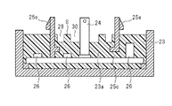
まず、図1を参照して本発明の第1の実施形態に係る電気システム1について説明する。なお、図1(b)は、コネクタ装置10と電気装置20が固定手段を介して互いに固定された状態(以下、単に「固定状態」ともいう。)における断面図を示している。
(First embodiment)
First, an
第1の実施形態に係る電気システム1は、コネクタ装置10と、このコネクタ装置10に電気的に接続される電気装置20とを備えている。電気装置20は、例えば、バイクや車等の車両のウィンカーを点滅させるウィンカーリレーである。なお、電気装置20はウィンカーリレーに限られず、他の電気装置であってもよい。
The
コネクタ装置10は、図1(b)に示すように、コネクタケース11と、コネクタ端子部12と、環状押圧部13とを有する。
As shown in FIG. 1B, the
コネクタケース11には、電気装置20に対向する面(図1(b)では下面)に凹部11aが設けられている。また、コネクタケース11には係合部11cが設けられている。この係合部11cは、例えばコネクタケース11の開口の縁部に設けられ(図1(b)参照)、電気装置20(端子ハウジング25の被係合部25e)に係合可能である。
The
コネクタ端子部12は、凹部11aの底面11bから突出するように設けられている。このコネクタ端子部12は、例えば、対向配置された2枚の板ばねから構成される。
The
環状押圧部13は、コネクタ端子部12を取り囲むように凹部11aの底面11bに環状に突設されている。なお、環状押圧部13は、樹脂成形等により、コネクタケース11と一体に形成されていてもよい。
The annular
電気装置20は、図1(a)に示すように、ケース21と、回路基板22と、封止部23と、端子部24と、端子ハウジング25とを有する。
As shown in FIG. 1A, the
ケース21は、一方(図1(a)では上方)が開口している。ケース21の材質は、例えば樹脂であるが、これに限らず金属等であってもよい。また、ケース21の形状は、例えば直方体形状であるが、これに限らず、円柱形状やその他の形状であってもよい。図1(a)に示すように、ケース21には、回路基板22を載置するための載置台27が設けられている。
One side (upper side in FIG. 1A) of the
回路基板22は、図1(a)に示すように、ケース21内に収容されている。回路基板22は、例えば、ガラスエポキシ基板、セラミック基板等である。また、回路基板22には、ICチップ、抵抗、コンデンサ、コイル等の電子部品26が実装されている。なお、図1(a)に示すように、端子ハウジング25の内側の領域に電子部品26が実装されていてもよい。
The
封止部23は、ケース21内に収容された回路基板22、および電子部品26を封止している。なお、電子部品26の種類によっては封止部23に埋設されなくてもよい。この封止部23は、弾性を有する。封止部23の材質は、特に限定されないが、例えば、エポキシ樹脂、ウレタン樹脂、アクリル樹脂、シリコーン等である。
The sealing
第1の実施形態では、図1(a)に示すように、封止部23の上面に、環状に窪んだ環状凹部28が形成されている。この環状凹部28の平面形状は、例えば円形または多角形であるが、これらに限定されるものではなく、環状に閉じていればよい。
In the first embodiment, as shown in FIG. 1A, an
環状凹部28は、ハウジング内封止部23aの上面に形成されている。ハウジング内封止部23aは封止部23の一部である。より詳しくは、ハウジング内封止部23aは、封止部23のうち、筒部25aの流通路25cを介して端子ハウジング25の外部の封止部と一体成形された部分である。例えば、ハウジング内封止部23aは、流通路25cを介して端子ハウジング25内に入り込んだ封止部である。このハウジング内封止部23aが従来のOリング等に相当する防水部材として機能する。
The
端子部24は、回路基板22の上に設けられ、上方に向けて延在する。この端子部24は、回路基板22の配線パターン(図示せず)に電気的に接続されている。なお、端子部24は、例えば電極(+,−)であるが、制御やモニタ用の端子であってもよい。また、端子部24の端子の数は2本に限らず、1本あるいは3本以上であってもよい。
The
端子ハウジング25は、図1(b)に示すように、端子部24を収容するように回路基板22上に設けられている。この端子ハウジング25は、封止部23の上面から突出した筒状の筒部25aを含む。この筒部25aには、コネクタ装置10の係合部11cに係合可能な被係合部25eが設けられている。なお、複数の被係合部25eが端子ハウジング25に対して略対称に設けられていることが好ましい。これにより、環状押圧部13が環状凹部28を押圧する力が均等化され、十分な防水能力を確保することができる。
As shown in FIG. 1B, the
筒部25aには流通路25cが設けられている。この流通路25cを介して、電気装置20の製造時にケース21内に注入された樹脂封止材が筒部25aの外部から内部へ(あるいは筒部25aの内部から外部へ)流通する。なお、流通路25cは、筒部25aの下端に切り欠き状に設けられているが、これに限らず、筒部25aの側面に貫通孔として設けられてもよい。
A
なお、端子ハウジング25は、上記の構成に限らず、一般的に言えば、端子ハウジング25は、上方に開口し、端子部24を収容するものであればよい。端子ハウジング25は、端子部24に固定され、一体の端子モジュールを構成してもよい。
Note that the
上記のコネクタ装置10と電気装置20は固定手段を介して互いに固定される。第1の実施形態では、固定手段はコネクタケース11の係合部11cと、端子ハウジング25の被係合部25eとから構成されている。図1(b)に示すように、係合部11cが被係合部25eに係合することにより、コネクタ装置10は電気装置20に固定される。
The
固定状態において、コネクタ端子部12は、図1(b)に示すように、端子部24に接触して電気的に接続される。例えば、電気装置20の端子部24は、コネクタ端子部12の2枚の板ばねに挟まれた状態となる。
In the fixed state, the
そして、固定状態において、コネクタ装置10の環状押圧部13は、図1(b)に示すように、弾性を有する封止部23の上面に形成された環状凹部28を押圧し弾性変形させる。より詳しくは、環状押圧部13がその環状の先端部の全周にわたって環状凹部28を押圧し弾性変形させることにより、防水構造が構成される。
In the fixed state, as shown in FIG. 1B, the annular pressing
よって、第1の実施形態によれば、Oリング等の防水部材を用いずに、すなわち追加コストを発生させずに防水構造を簡易に構成することができる。さらに、第1の実施形態によれば、環状凹部28によって外部からの水の浸入経路が長くなるため、防水性能を向上させることができる。
Therefore, according to the first embodiment, the waterproof structure can be easily configured without using a waterproof member such as an O-ring, that is, without generating additional costs. Furthermore, according to the first embodiment, the water penetration path from the outside is lengthened by the
次に、第1の実施形態に係る変形例1〜5について説明する。いずれの変形例によっても、第1の実施形態と同様の効果を得ることができる。
Next,
<変形例1>
本変形例では、環状凹部28の幅がコネクタ装置10の環状押圧部13の厚さよりも小さく、図2に示すように、固定状態において、コネクタ装置10の環状押圧部13は環状凹部28に圧入される。これにより、環状押圧部13は底面だけでなく側面においても環状凹部28に接することになるため、防水性能を向上させることができる。
<
In this modification, the width of the
<変形例2>
本変形例では、図3(a)に示すように、環状凹部28の底面に、環状に突出した凹部内突部29が形成されている。そして、固定状態において、図3(b)に示すように、コネクタ装置10の環状押圧部13は凹部内突部29を押圧して弾性変形させる。本変形例によれば、環状凹部28に対する環状押圧部13の押圧力が増加する結果、防水性能を向上させることができる。
<
In this modified example, as shown in FIG. 3A, an
<変形例3>
本変形例では、図4に示すように、環状凹部28に加えて、環状凹部28より端子部24側の封止部23の上面に中央凹部30が形成されている。そして、固定状態において、コネクタ装置10の環状押圧部13は、環状凹部28ではなく環状領域Sを押圧する。環状領域Sは、封止部23の上面のうち、環状凹部28と中央凹部30に挟まれた領域である。環状領域Sは、環状凹部28と中央凹部30により挟まれているため、上方からの押圧力に対して弾性変形し易い。よって、本変形例によれば、環状押圧部13と封止部23との接触面積が増え、その結果、防水性能を向上させることができる。
<Modification 3>
In this modified example, as shown in FIG. 4, in addition to the
<変形例4>
本変形例では、図5に示すように、端子ハウジング25は、封止部23内に配置された底部25bと、封止部23の上面から突出する内側筒部25dとをさらに有する。底部25bは、筒部25aの内周面に突設されている。この底部25bは、周方向に延在している。また、底部25bには、貫通孔25b1が設けられている。内側筒部25dは、底部25bの上面に環状に突設され、端子部24を取り囲むように構成されている。なお、本変形例において、ハウジング内封止部23aは、封止部23のうち、筒部25aの流通路25cおよび底部25bの貫通孔25b1を介して端子ハウジング25の外部の封止部と一体成形された部分である。
<Modification 4>
In the present modification, as shown in FIG. 5, the
本変形例によれば、端子ハウジング25に設けられた内側筒部25dにより、外部からの水の浸入経路が長くなるため、防水性能を向上させることができる。
According to this modification, the
<変形例5>
本変形例では、図6に示すように、端子ハウジング25は、封止部23内に配置され、筒部25aの内周面に突設された底部25bをさらに有する。ただし、筒部25aには流通路25cが設けられておらず、底部25bには貫通孔25b1が設けられていない。本変形例のハウジング内封止部23aは、端子ハウジング25の外部の封止部と一体成形されたものではなく、別の工程で形成されたものである。
<Modification 5>
In the present modification, as shown in FIG. 6, the
また、図6に示すように、ハウジング内封止部23aの上面は、端子ハウジング25の外部の封止部23よりも高く、これに合わせて環状凹部28の底面も高い。これにより、環状凹部28に対する環状押圧部13の押圧力が増加し、その結果、防水性能を向上させることができる。
As shown in FIG. 6, the upper surface of the in-
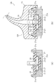
(電気装置20の製造方法)
次に、上記の電気装置20の製造方法について図7Aおよび図7Bを参照して説明する。
(Method for manufacturing electric device 20)
Next, a method for manufacturing the
まず、図7A(1)に示すように、電子部品26、端子部24および端子ハウジング25を回路基板22に実装する(実装工程)。例えば、端子部24および電子部品26を回路基板22上に実装した後、端子ハウジング25を回路基板22に載置する。なお、端子部24と端子ハウジング25が一体の端子モジュールを構成している場合は、一体の端子モジュールを回路基板22に実装する。
First, as shown in FIG. 7A (1), the
次に、図7A(2)に示すように、電子部品26、端子部24および端子ハウジング25が実装された回路基板22を、上方が開口したケース21内に端子部24が上方に向くように収容する(収容工程)。この際、回路基板22はケース21の載置台27の上に載置される。
Next, as shown in FIG. 7A (2), the
次に、環状凹部28を形成するための治具40を用意する。この治具40は、図7B(a),(b)に示すように、本体部41および環状凹部形成部42を有する。本体部41には、上面41aから下面41bに貫通する空気逃がし孔43が設けられている。環状凹部形成部42は、空気逃し孔43の、本体部41の下面41bにおける開口を取り囲むように下面41bに環状に突設されている。環状凹部形成部42の長さおよび厚さは、環状凹部28の所望の深さおよび幅に応じて決められる。例えば、図2で説明したように環状押圧部13を環状凹部28に圧入させる場合には、環状凹部形成部42の厚さは環状押圧部13の厚さよりも小さくする。
Next, a
次に、図7B(b)に示すように、端子部24が環状凹部形成部42内に配置されるように治具40を端子ハウジング25に取り付ける。ここでは、治具40は、端子ハウジング25の上端開口部に載置される。なお、治具40は、図8に示すように、端子ハウジング25の被係合部25eに係合可能な係合部44を有してもよい。この場合、治具40は、本工程において、係合部44が被係合部25eに係合することにより端子ハウジング25に固定される。これにより、後段の樹脂封止材の注入工程を安定して行うことができる。
Next, as shown in FIG. 7B (b), the
次に、図7B(b)および図8に示すように、回路基板22が埋設され且つ環状凹部形成部42の少なくとも先端部が浸るように、ケース21内に樹脂封止材を注入する(注入工程)。治具40には空気逃がし孔43が設けられているため、環状凹部形成部42の内側の空間に樹脂封止材を注入することができる。なお、本工程で注入する樹脂封止材としては、例えば熱硬化性樹脂(エポキシ樹脂、ウレタン樹脂、アクリル樹脂、シリコーン等)を用いる。
Next, as shown in FIGS. 7B (b) and 8, a resin sealing material is injected into the
樹脂封止材は、ケース21と端子ハウジング25との間(図7B(a)の注入位置F1)からケース21内に注入される。この場合、ケース21内に注入された樹脂封止材は、回路基板22を埋設した後、端子ハウジング25の流通路25cを通って端子ハウジング25の内部に浸入することになる。すなわち、注入工程において、ケース21内に樹脂封止材を注入し、流通路25cを介して端子ハウジング25の内部に樹脂封止材を入り込ませる。
The resin sealing material is injected into the
なお、端子ハウジング25の流通路25cの大きさや数、樹脂封止材の注入速度によっては、端子ハウジング25(図7B(a)の注入位置F2)からケース21内に樹脂封止材を注入するようにしてもよい。この場合、端子ハウジング25から注入された樹脂封止材は、流通路25cを通って端子ハウジング25の外部に流出し、ケース21内を充填することになる。
Depending on the size and number of the
次に、注入工程において注入された樹脂封止材を硬化させて弾性を有する封止部23を形成する(硬化工程)。端子ハウジング25内の樹脂封止材は硬化してハウジング内封止部23aとなる。封止部23が形成された後、治具40を端子ハウジング25から取り外して、封止部23の上面に環状に窪んだ環状凹部28を形成する。
Next, the resin sealing material injected in the injection step is cured to form the sealing
なお、図6を参照して説明した第5の変形例のように、端子ハウジング25に流通路25cが設けられていない場合は、樹脂封止材の注入を端子ハウジング25の外部と内部の2回に分けて行う。この場合、端子ハウジング25内に樹脂封止材を注入する工程が新たに追加されることになるが、樹脂封止材の注入位置を少し変えるだけであるため、大きな追加コストを発生させることはなくハウジング内封止部23aを形成することができる。
As in the fifth modification described with reference to FIG. 6, when the
また、端子ハウジング25を実装するタイミングは、上記の実装工程に限るものではない。例えば、ケース21内に回路基板22を収容した後でもよいし、あるいは、ケース21内に樹脂封止材を注入している途中もしくは注入完了後であってもよい。
Moreover, the timing which mounts the
(第2の実施形態)
次に、本発明の第2の実施形態に係る電気システム1Aについて説明する。第2の実施形態の第1の実施形態との相違点の一つは、電気装置が端子ハウジングを有しない点である。以下、第1の実施形態との相違点を中心に第2の実施形態について説明する。
(Second Embodiment)
Next, an
第2の実施形態に係る電気システム1Aは、図9(b)に示すように、コネクタ装置10Aと、このコネクタ装置10Aに電気的に接続される電気装置20Aとを備えている。
As shown in FIG. 9B, the
コネクタ装置10Aは、コネクタケース15と、コネクタ端子部16と、環状押圧部17とを有する。
The
コネクタケース15は、電気装置20Aに対向する面(図9(b)では下面)に凹部15aが設けられている。また、コネクタケース15には係合部15cが設けられている。この係合部15cは、例えばコネクタケース15の開口の縁部に設けられており、電気装置20A(の被係合部21a)に係合可能である。
The
コネクタ端子部16は、凹部15aの底面15bから突出するように設けられている。このコネクタ端子部16は、例えば、対向配置された2枚の板ばねから構成される。
The
環状押圧部17は、コネクタ端子部16を取り囲むように凹部15aの底面15bに環状に突設されている。なお、環状押圧部17は、樹脂成形等により、コネクタケース15と一体に形成されていてもよい。
The annular pressing portion 17 is provided in a ring shape on the
電気装置20Aは、図9(a)に示すように、ケース21と、回路基板22と、封止部23と、端子部24とを有するが、端子ハウジング25は有しない。
As illustrated in FIG. 9A, the
ケース21には、コネクタケース15の係合部15cに係合可能な被係合部21aが設けられている。被係合部21aは、第1の実施形態で説明した被係合部25eと同様に、ケース21に対して略対称となる位置に複数設けられている。これにより、環状押圧部17が封止部23の環状凹部28を押圧する力が均等化され、十分な防水能力を確保することができる。なお、第2の実施形態に係る電気装置20Aは、第1の実施形態で説明した製造方法と同様の方法により製造することが可能である。この場合、治具40はケース21に取り付けられる。
The
上記のコネクタ装置10Aと電気装置20Aは固定手段を介して互いに固定される。第2の実施形態では、固定手段は、コネクタケース15の係合部15cと、ケース21の被係合部21aとから構成されている。図9(b)に示すように、係合部15cが被係合部21aに係合することにより、コネクタ装置10Aは電気装置20Aに固定される。固定状態において、コネクタ端子部16は端子部24に接触して電気的に接続され、環状押圧部17は、弾性を有する封止部23の上面に形成された環状凹部28を押圧し弾性変形させる。より詳しくは、環状押圧部17がその環状の先端部の全周にわたって環状凹部28を押圧し弾性変形させることにより、防水構造が構成される。
The
よって、第2の実施形態によれば、第1の実施形態と同様に、追加コストを発生させずに防水構造を簡易に構成することができる。また、環状凹部28によって外部からの水の浸入経路が長くなるため、防水性能を向上させることができる。
Therefore, according to the second embodiment, similarly to the first embodiment, the waterproof structure can be easily configured without generating an additional cost. Moreover, since the intrusion path | route of the water from the outside becomes long with the cyclic | annular recessed
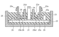
(第3の実施形態)
次に、本発明の第3の実施形態に係る電気システム1Bについて説明する。第3の実施形態の第1の実施形態との相違点の一つは、環状凹部の代わりに環状突部が封止部の上面に形成されている点である。以下、第1の実施形態との相違点を中心に第3の実施形態について説明する。
(Third embodiment)
Next, an
第3の実施形態に係る電気システム1Bは、図10(b)に示すように、コネクタ装置10と、このコネクタ装置10に電気的に接続される電気装置20Bとを備えている。コネクタ装置10については、第1の実施形態と同様であるため、詳しい説明を省略する。
As shown in FIG. 10B, the
電気装置20Bは、図10(a)に示すように、ケース21と、回路基板22と、封止部23と、端子部24と、端子ハウジング25とを有する。
As illustrated in FIG. 10A, the
図10(a)に示すように、封止部23の上面には、環状に突出した環状突部31が形成されている。本実施形態では、環状突部31はハウジング内封止部23aの上面に形成されている。
As shown in FIG. 10A, an
環状突部31は、封止部23と同様に弾性を有する。環状突部31の平面形状は、例えば円形または多角形であるが、これらに限定されるものではなく、環状に閉じていればよい。
The
なお、外部からの水の浸入経路を長くするために、環状突部31に加えて、第1の実施形態で説明した環状凹部28が設けられてもよい。また、第3の実施形態においても第2の実施形態と同様に、電気装置が端子ハウジング25を有しない構成を想定することが可能である。
In addition to the
固定状態において、コネクタ装置10の環状押圧部13は、図10(b)に示すように、封止部23(ハウジング内封止部23a)の上面に形成された環状突部31を押圧し弾性変形させる。より詳しくは、環状押圧部13がその環状の先端部の全周にわたって環状突部31を押圧し弾性変形させることにより、防水構造が構成される。
In the fixed state, as shown in FIG. 10B, the annular pressing
よって、第3の実施形態によれば、第1および第2の実施形態と同様に、追加コストを発生させずに防水構造を簡易に構成することができる。また、環状突部31によって外部からの水の浸入経路が長くなるため、防水性能を向上させることができる。
Therefore, according to the third embodiment, similarly to the first and second embodiments, the waterproof structure can be easily configured without generating additional costs. Moreover, since the intrusion path | route of the water from the outside becomes long with the cyclic |
次に、第3の実施形態に係る変形例1〜3について説明する。いずれの変形例によっても、第3の実施形態と同様の効果を得ることができる。 Next, modified examples 1 to 3 according to the third embodiment will be described. In any of the modifications, the same effect as that of the third embodiment can be obtained.
<変形例1>
本変形例では、図11(a)に示すように、コネクタ装置10Bの環状押圧部13の先端部には、凹部11aの底面11b側に窪んだ先端凹部13aが形成されている。そして、図11(b)に示すように、環状押圧部13は、固定状態において、環状の先端凹部13aにより環状突部31の先端を覆いつつ環状突部31を押圧する。これにより、環状押圧部13は安定的に環状突部31を押圧して弾性変形させることができる。より詳しくは、環状押圧部13から押圧力を受ける環状突部31が座屈変形した場合であっても、環状突部31を押圧し続けることができ、防水能力を維持できる。
<
In this modification, as shown in FIG. 11A, a
さらに、環状押圧部13は環状突部31の上端角部においても接することから、環状押圧部13と環状突部31との間の接触面積が増加し、防水性能を向上させることができる。
Furthermore, since the annular pressing
<変形例2>
本変形例では、図12(a)に示すように、電気装置20Cの端子ハウジング25は内側筒部25dを有し、環状突部31は内側筒部25dのうち封止部23の上面から突出した部位を覆うように形成されている。これにより、端子ハウジング25の平面サイズを増やすことなく、環状突部31を形成することができる。また、環状突部31の内部に内側筒部25dが芯として存在するため、環状押圧部13から受ける押圧力によって環状突部31が座屈変形することを抑制できる。
<
In this modified example, as shown in FIG. 12A, the
<変形例3>
本変形例は、上記の変形例1と変形例2を組み合わせたものである。図13に示すように、環状押圧部13の先端部には先端凹部13aが形成されるとともに、環状突部31は内側筒部25dのうち封止部23の上面から突出した部位を覆うように形成されている。
<Modification 3>
This modification is a combination of
次に、第3の実施形態および変形例に係る電気装置20B,20Cの2つの製造方法について説明する。いずれの製造方法についても、実装工程および収容工程については第1の実施形態に係る電気装置の場合と同様であるので説明を省略し、収容工程の次の工程から説明する。
Next, two manufacturing methods of the
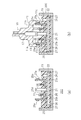
(電気装置20Bの第1の製造方法)
まず、第1の製造方法について、図14(a),(b)を参照して説明する。本製造方法では、ケース21内に注入した樹脂封止材を吸引する方式で環状突部31を形成する。
(First manufacturing method of
First, the first manufacturing method will be described with reference to FIGS. 14 (a) and 14 (b). In this manufacturing method, the
環状突部31を形成するための治具50を用意する。この治具50は、図14(a)に示すように、本体部51および環状突部形成部52を有する。環状突部形成部52は、本体部51の下面51bに環状に突設されている。また、環状突部形成部52の先端部には、当該先端部に沿って環状の先端凹部52aが形成されている。さらに、治具50には、先端凹部52aの底面から本体部51の上面51aに貫通する貫通孔53が設けられている。
A
なお、本体部51の形状は、図14(a)に示すものに限られない。例えば、コーナー部Cを設けずに、本体部51から環状突部形成部52に向かってなだらかに縮径するテーパー形状としてもよい。
In addition, the shape of the main-
また、治具50の材質は特に限定されないが、離型性の良い絶縁材料からなることが好ましい。例えば、治具50は、ポリプロピレン等を含む絶縁材料から機械加工で切り出すことにより形成される。あるいは、金属材料を用いて治具50を形成してもよい。この場合、環状突部形成部52の先端部に離型剤を塗布するか、環状突部形成部52の先端部をポリプロピレン等の離型性の良い樹脂で被覆することが好ましい。
Further, the material of the
次に、図14(b)に示すように、端子部24が環状突部形成部52内に配置されるように治具50を端子ハウジング25に取り付ける。治具50は、端子ハウジング25の上端開口部に載置される。なお、治具50は、端子ハウジング25の被係合部25eに係合可能な係合部(図示せず)を有し、端子ハウジング25に固定されてもよい。あるいは、環状突部形成部52の外径を筒部25aの内径に略等しくして、治具50が筒部25aに圧入固定されるようにしてもよい。
Next, as shown in FIG. 14B, the
次に、回路基板22が埋設され且つ環状突部形成部52の先端部が浸るまでケース21内に樹脂封止材を注入する(注入工程)。より詳しくは、後段の真空引き工程での樹脂封止材の吸引量に応じて、環状突部形成部52の下端から所定の高さまで樹脂封止材を注入する。なお、樹脂封止材は、第1の実施形態と同様に、ケース21と端子ハウジング25との間からケース21内に注入してもよいし、あるいは、端子ハウジング25からケース21内に樹脂封止材を注入してもよい。
Next, a resin sealing material is injected into the
次に、治具50にポンプを接続し、治具50の貫通孔53から真空引きを行って、先端凹部52a内を樹脂封止材で充填する(真空引き工程)。
Next, a pump is connected to the
真空引き工程の後、ケース21内に注入された樹脂封止材および先端凹部52a内に充填された樹脂封止材を硬化させて、回路基板22を封止し弾性を有する封止部23、および封止部23の上面に環状に突出した環状突部31を形成する(硬化工程)。硬化工程の後、治具50を端子ハウジング25から取り外す。
After the evacuation step, the resin sealing material injected into the
なお、上記の製造工程において、端子ハウジング25への治具50の取り付けは、実装工程の後、かつ収容工程の前に行ってもよい。
In the above manufacturing process, the
(電気装置20Bの第2の製造方法)
次に、電気装置20B(20C)の第2の製造方法について図15(a),(b)を参照して説明する。本製造方法では、樹脂封止材の二度入れ方式により封止部23および環状突部31を形成する。
(Second Manufacturing Method of
Next, a second manufacturing method of the
収容工程の後、図15(a)に示すように、回路基板22が埋設されるように、ケース21内に所定の充填レベル(高さ)Hまで樹脂封止材を注入する(第1注入工程)。ここで、所定の充填レベルHは、端子ハウジング25に治具50を取り付けた状態において、治具50の環状突部形成部52が樹脂封止材の上面に接するように決められる。
After the accommodating step, as shown in FIG. 15A, a resin sealing material is injected into the
前述の治具50を用意した後、図15(b)に示すように、端子部24が環状突部形成部52内に配置されるように治具50を端子ハウジング25に取り付ける。
After the
次に、第1注入工程で注入した樹脂封止材の少なくとも上面を硬化させる。その後、図15(b)に示すように、治具50の貫通孔53から樹脂封止材を注入し、環状突部形成部52の先端凹部52a内を樹脂封止材で充填する(第2注入工程)。
Next, at least the upper surface of the resin sealing material injected in the first injection step is cured. Thereafter, as shown in FIG. 15 (b), a resin sealing material is injected from the through
次に、第1および第2注入工程で注入された樹脂封止材を硬化させて、回路基板22を封止し弾性を有する封止部23、および封止部23の上面に環状に突出した環状突部31を形成する(硬化工程)。硬化工程の後、治具50を端子ハウジング25から取り外す。
Next, the resin sealing material injected in the first and second injection steps is cured to seal the
上記の記載に基づいて、当業者であれば、本発明の追加の効果や種々の変形を想到できるかもしれないが、本発明の態様は、上述した個々の実施形態に限定されるものではない。異なる実施形態にわたる構成要素を適宜組み合わせてもよい。特許請求の範囲に規定された内容及びその均等物から導き出される本発明の概念的な思想と趣旨を逸脱しない範囲で種々の追加、変更及び部分的削除が可能である。 Based on the above description, those skilled in the art may be able to conceive additional effects and various modifications of the present invention, but the aspects of the present invention are not limited to the individual embodiments described above. . You may combine suitably the component covering different embodiment. Various additions, modifications, and partial deletions can be made without departing from the concept and spirit of the present invention derived from the contents defined in the claims and equivalents thereof.
1,1A,1B 電気システム
10,10A,10B コネクタ装置
11,15 コネクタケース
11a,15a 凹部
11b,15b (凹部の)底面
11c,15c 係合部
12,16 コネクタ端子部
13,17 環状押圧部
13a 先端凹部
20,20A,20B,20C 電気装置
21,21A ケース
21a 被係合部
22 回路基板
23 封止部
23a ハウジング内封止部
24 端子部
25 端子ハウジング
25a 筒部
25b 底部
25b1 貫通孔
25c 流通路
25d 内側筒部
25e 被係合部
26 電子部品
27 (ケースの)載置台
28 (封止部の)環状凹部
29 凹部内突部
30 中央凹部
31 (封止樹脂の)環状突部
40 (環状凹部形成用の)治具
41 本体部
41a 上面
41b 下面
42 環状凹部形成部
43 空気逃がし孔
44 係合部
50 (環状突部形成用の)治具
51 本体部
51a 上面
51b 下面
52 環状突部形成部
52a 先端凹部
53 貫通孔
C コーナー部
F1,F2 樹脂注入位置
H 充填レベル
S 環状領域
1, 1A,
Claims (13)
前記コネクタ装置は、
前記電気装置に対向する下面に凹部が設けられたコネクタケースと、
前記凹部の底面から突出するように設けられたコネクタ端子部と、
前記コネクタ端子部を取り囲むように前記凹部の前記底面に環状に突設された環状押圧部と、を有し、
前記電気装置は、
上方が開口したケースと、
電子部品が実装され、前記ケース内に収容された回路基板と、
前記ケース内に収容された前記回路基板を封止し、弾性を有する封止部と、
前記回路基板の上に設けられ、上方に向けて延在する端子部と、を有し、
前記封止部の上面に、環状に窪んだ環状凹部または環状に突出した環状突部が形成され、
前記コネクタ装置と前記電気装置とが固定手段を介して互いに固定された固定状態において、前記コネクタ端子部は前記端子部に接触して電気的に接続され、前記環状押圧部は、前記環状凹部または前記環状突部を押圧し弾性変形させることを特徴とする電気システム。 An electrical system comprising a connector device and an electrical device electrically connected to the connector device,
The connector device includes:
A connector case provided with a recess on the lower surface facing the electrical device;
A connector terminal portion provided so as to protrude from the bottom surface of the recess;
An annular pressing portion projecting annularly on the bottom surface of the recess so as to surround the connector terminal portion,
The electrical device is
A case with an open top;
A circuit board on which electronic components are mounted and housed in the case;
Sealing the circuit board housed in the case, and having a sealing portion having elasticity;
A terminal portion provided on the circuit board and extending upward;
On the upper surface of the sealing portion, an annular recess recessed annularly or an annular protrusion projecting annularly is formed,
In the fixed state in which the connector device and the electric device are fixed to each other via fixing means, the connector terminal portion is in contact with and electrically connected to the terminal portion, and the annular pressing portion is the annular recess or An electric system, wherein the annular protrusion is pressed and elastically deformed.
前記環状凹部または前記環状突部は、前記封止部のうち、前記端子ハウジングの外部の封止部と一体成形されたハウジング内封止部の上面に形成されていることを特徴とする請求項6に記載の電気システム。 The terminal housing is provided on the circuit board so as to accommodate the terminal portion, and includes a cylindrical tube portion protruding from an upper surface of the sealing portion,
The said annular recessed part or the said annular protrusion is formed in the upper surface of the sealing part in a housing integrally molded with the sealing part outside the said terminal housing among the said sealing parts. 7. The electrical system according to 6.
前記コネクタ装置は、前記電気装置に対向する下面に凹部が設けられたコネクタケースと、前記凹部の底面から突出するように設けられたコネクタ端子部と、前記コネクタ端子部を取り囲むように前記凹部の前記底面に環状に突設された環状押圧部とを有し、
前記電気装置は、
上方が開口したケースと、
電子部品が実装され、前記ケース内に収容された回路基板と、
前記ケース内に収容された前記回路基板を封止し、弾性を有する封止部と、
前記回路基板の上に設けられ、上方に向けて延在する端子部と、を有し、
前記封止部の上面に、環状に窪んだ環状凹部または環状に突出した環状突部が形成され、
前記コネクタ装置と前記電気装置とが固定手段を介して互いに固定された固定状態において、前記コネクタ端子部は前記端子部に接触して電気的に接続され、前記環状押圧部は、前記環状凹部または前記環状突部を押圧し弾性変形させることを特徴とする電気装置。 An electrical device electrically connected to the connector device,
The connector device includes a connector case provided with a recess on a lower surface facing the electrical device, a connector terminal portion provided so as to protrude from the bottom surface of the recess, and the recess portion so as to surround the connector terminal portion. An annular pressing portion projecting annularly on the bottom surface,
The electrical device is
A case with an open top;
A circuit board on which electronic components are mounted and housed in the case;
Sealing the circuit board housed in the case, and having a sealing portion having elasticity;
A terminal portion provided on the circuit board and extending upward;
On the upper surface of the sealing portion, an annular recess recessed annularly or an annular protrusion projecting annularly is formed,
In the fixed state in which the connector device and the electric device are fixed to each other via fixing means, the connector terminal portion is in contact with and electrically connected to the terminal portion, and the annular pressing portion is the annular recess or An electric device, wherein the annular protrusion is pressed and elastically deformed.
上面から下面に貫通する空気逃がし孔が設けられた本体部と、前記空気逃し孔の前記下面における開口を取り囲むように前記下面に環状に突設された環状凹部形成部とを有する治具を用意し、前記端子部が前記環状凹部形成部内に配置されるように前記治具を前記端子ハウジングに取り付ける工程と、
前記回路基板が埋設され且つ前記環状凹部形成部の少なくとも先端部が浸るように、前記ケース内に樹脂封止材を注入する注入工程と、
前記注入された樹脂封止材を硬化させて弾性を有する封止部を形成する硬化工程と、
前記硬化工程の後、前記治具を前記端子ハウジングから取り外して、前記封止部の上面に環状に窪んだ環状凹部を形成する工程と、
を備えることを特徴とする電気装置の製造方法。 A step of accommodating the circuit board on which the electronic component, the terminal portion, and the terminal housing are mounted so that the terminal portion faces upward in a case having an upper opening;
A jig having a main body portion provided with an air escape hole penetrating from the upper surface to the lower surface and an annular recess forming portion projecting annularly on the lower surface so as to surround the opening of the lower surface of the air escape hole is prepared. And attaching the jig to the terminal housing such that the terminal part is disposed in the annular recess forming part,
An injection step of injecting a resin sealing material into the case so that the circuit board is embedded and at least the tip of the annular recess forming portion is immersed;
A curing step of curing the injected resin sealing material to form a sealing portion having elasticity;
After the curing step, removing the jig from the terminal housing and forming an annular recess that is annularly recessed on the upper surface of the sealing portion;
An electrical device manufacturing method comprising:
本体部と、前記本体部の下面に環状に突設された環状突部形成部とを有し、前記環状突部形成部の先端部には環状の先端凹部が形成され、前記先端凹部から前記本体部に貫通する貫通孔が設けられた治具を用意し、前記端子部が前記環状突部形成部内に配置されるように前記治具を前記端子ハウジングに取り付ける工程と、
前記回路基板が埋設され且つ前記環状突部形成部の先端部が浸るまで前記ケース内に樹脂封止材を注入する注入工程と、
前記治具の前記貫通孔から真空引きを行って、前記先端凹部内を前記樹脂封止材で充填する真空引き工程と、
前記真空引き工程の後、前記樹脂封止材を硬化させて、前記回路基板を封止し弾性を有する封止部、および前記封止部の上面に環状に突出した環状突部を形成する硬化工程と、
前記硬化工程の後、前記治具を前記端子ハウジングから取り外す工程と、
を備えることを特徴とする電気装置の製造方法。 A step of accommodating the circuit board on which the electronic component, the terminal portion, and the terminal housing are mounted so that the terminal portion faces upward in a case having an upper opening;
A main body portion and an annular protrusion forming portion projecting annularly on the lower surface of the main body portion, and an annular tip recess is formed at the tip of the annular protrusion forming portion. Preparing a jig provided with a through-hole penetrating the main body, and attaching the jig to the terminal housing such that the terminal part is disposed in the annular protrusion forming part;
An injection step of injecting a resin sealing material into the case until the circuit board is embedded and the tip of the annular protrusion forming portion is immersed;
Evacuating from the through hole of the jig, and filling the inside of the concave portion with the resin sealing material;
After the evacuation step, the resin sealing material is cured to form a sealing portion that seals the circuit board and has elasticity, and an annular protrusion that protrudes in an annular shape on the top surface of the sealing portion. Process,
After the curing step, removing the jig from the terminal housing;
An electrical device manufacturing method comprising:
前記回路基板が埋設されるように、前記ケース内に所定の充填レベルまで樹脂封止材を注入する第1注入工程と、
本体部と、前記本体部の下面に環状に突設された環状突部形成部とを有し、前記環状突部形成部の先端部には環状の先端凹部が形成され、前記先端凹部から前記本体部に貫通する貫通孔が設けられた治具を用意し、前記端子部が前記環状突部形成部内に配置されるように前記治具を前記端子ハウジングに取り付ける工程と、
前記第1注入工程で注入した樹脂封止材の少なくとも上面が硬化した後、前記治具の前記貫通孔から樹脂封止材を注入し、前記先端凹部内を樹脂封止材で充填する第2注入工程と、
前記第1および第2注入工程で注入された樹脂封止材を硬化させて、前記回路基板を封止し弾性を有する封止部、および前記封止部の上面に環状に突出した環状突部を形成する硬化工程と、
前記硬化工程の後、前記治具を前記端子ハウジングから取り外す工程と、
を備えることを特徴とする電気装置の製造方法。 A step of accommodating the circuit board on which the electronic component, the terminal portion, and the terminal housing are mounted so that the terminal portion faces upward in a case having an upper opening;
A first injection step of injecting a resin sealing material up to a predetermined filling level in the case so that the circuit board is embedded;
A main body portion and an annular protrusion forming portion projecting annularly on the lower surface of the main body portion, and an annular tip recess is formed at the tip of the annular protrusion forming portion. Preparing a jig provided with a through-hole penetrating the main body, and attaching the jig to the terminal housing such that the terminal part is disposed in the annular protrusion forming part;
After at least the upper surface of the resin sealing material injected in the first injection step is cured, the resin sealing material is injected from the through hole of the jig, and the inside of the tip recess is filled with the resin sealing material. An injection process;
The resin sealing material injected in the first and second injection steps is cured to seal the circuit board and have elasticity, and an annular protrusion protruding annularly on the upper surface of the sealing portion A curing step to form,
After the curing step, removing the jig from the terminal housing;
An electrical device manufacturing method comprising:
Priority Applications (1)
| Application Number | Priority Date | Filing Date | Title |
|---|---|---|---|
| JP2015169711A JP6498570B2 (en) | 2015-08-28 | 2015-08-28 | Electrical system, electrical device, and method of manufacturing electrical device |
Applications Claiming Priority (1)
| Application Number | Priority Date | Filing Date | Title |
|---|---|---|---|
| JP2015169711A JP6498570B2 (en) | 2015-08-28 | 2015-08-28 | Electrical system, electrical device, and method of manufacturing electrical device |
Publications (2)
| Publication Number | Publication Date |
|---|---|
| JP2017045699A JP2017045699A (en) | 2017-03-02 |
| JP6498570B2 true JP6498570B2 (en) | 2019-04-10 |
Family
ID=58210361
Family Applications (1)
| Application Number | Title | Priority Date | Filing Date |
|---|---|---|---|
| JP2015169711A Active JP6498570B2 (en) | 2015-08-28 | 2015-08-28 | Electrical system, electrical device, and method of manufacturing electrical device |
Country Status (1)
| Country | Link |
|---|---|
| JP (1) | JP6498570B2 (en) |
Families Citing this family (2)
| Publication number | Priority date | Publication date | Assignee | Title |
|---|---|---|---|---|
| FR3065588B1 (en) * | 2017-04-25 | 2019-06-21 | Jtekt Europe | WIRING METHOD INCLUDING A COATING STEP OF NON-SEALED CONNECTORS IN A RESIN |
| JP7474959B2 (en) * | 2019-06-11 | 2024-04-26 | パナソニックIpマネジメント株式会社 | Electronic component connection structure |
Family Cites Families (4)
| Publication number | Priority date | Publication date | Assignee | Title |
|---|---|---|---|---|
| JP5082405B2 (en) * | 2006-11-24 | 2012-11-28 | いすゞ自動車株式会社 | Harness grommet |
| JP5564844B2 (en) * | 2009-07-21 | 2014-08-06 | 株式会社デンソー | Electronic equipment |
| JP2011204482A (en) * | 2010-03-25 | 2011-10-13 | Panasonic Electric Works Co Ltd | Discharge lamp lighting device |
| JP6329475B2 (en) * | 2014-10-09 | 2018-05-23 | 株式会社畑屋製作所 | Waterproof outlet |
-
2015
- 2015-08-28 JP JP2015169711A patent/JP6498570B2/en active Active
Also Published As
| Publication number | Publication date |
|---|---|
| JP2017045699A (en) | 2017-03-02 |
Similar Documents
| Publication | Publication Date | Title |
|---|---|---|
| JP2019016689A (en) | Electronic control device and manufacturing method thereof | |
| KR200482547Y1 (en) | Waterproof ear-connector | |
| CN207925774U (en) | Socket connector | |
| JP4779614B2 (en) | Semiconductor device | |
| JP2015512116A (en) | Method for the manufacture of control equipment casings and control equipment casings produced by this method | |
| JP6498570B2 (en) | Electrical system, electrical device, and method of manufacturing electrical device | |
| JP6844455B2 (en) | Circuit equipment | |
| CN105611774A (en) | System including sensor and electrical cable | |
| JP2011060627A (en) | Electronic component | |
| JP6639487B2 (en) | Part with at least one opening | |
| JP2013069832A (en) | Control device of apparatus | |
| JP2006013170A (en) | Electronic component and method for manufacturing electronic component | |
| CN101320700B (en) | Method and molding tool for manufacturing electronic device having resin molded case | |
| JP6366071B2 (en) | Electronic equipment | |
| JP6897332B2 (en) | connector | |
| JP4960923B2 (en) | Electronic device and manufacturing method thereof | |
| JP4912350B2 (en) | Manufacturing method of electronic device | |
| JP2018133421A (en) | Electronic unit | |
| JP2017033767A (en) | Electric system, electric device, and manufacturing method of electric device | |
| KR102679404B1 (en) | Menufacturing method for socketshellless-type soketconnector | |
| KR100843356B1 (en) | Insert Injection Molding Terminal | |
| JP2016115697A (en) | Electronic device | |
| JP6292868B2 (en) | Batch molding module | |
| JP5358056B2 (en) | Electronic component equipment | |
| JP2013115265A (en) | Resin sealed module and method of manufacturing the same |
Legal Events
| Date | Code | Title | Description |
|---|---|---|---|
| A621 | Written request for application examination |
Free format text: JAPANESE INTERMEDIATE CODE: A621 Effective date: 20180222 |
|
| TRDD | Decision of grant or rejection written | ||
| A01 | Written decision to grant a patent or to grant a registration (utility model) |
Free format text: JAPANESE INTERMEDIATE CODE: A01 Effective date: 20190212 |
|
| A61 | First payment of annual fees (during grant procedure) |
Free format text: JAPANESE INTERMEDIATE CODE: A61 Effective date: 20190313 |
|
| R150 | Certificate of patent or registration of utility model |
Ref document number: 6498570 Country of ref document: JP Free format text: JAPANESE INTERMEDIATE CODE: R150 |