JP6495025B2 - Vacuum integrated hard mask processing and equipment - Google Patents
Vacuum integrated hard mask processing and equipment Download PDFInfo
- Publication number
- JP6495025B2 JP6495025B2 JP2015016254A JP2015016254A JP6495025B2 JP 6495025 B2 JP6495025 B2 JP 6495025B2 JP 2015016254 A JP2015016254 A JP 2015016254A JP 2015016254 A JP2015016254 A JP 2015016254A JP 6495025 B2 JP6495025 B2 JP 6495025B2
- Authority
- JP
- Japan
- Prior art keywords
- metal
- containing film
- module
- patterning
- film
- Prior art date
- Legal status (The legal status is an assumption and is not a legal conclusion. Google has not performed a legal analysis and makes no representation as to the accuracy of the status listed.)
- Active
Links
- 238000012545 processing Methods 0.000 title claims description 29
- 229910052751 metal Inorganic materials 0.000 claims description 124
- 239000002184 metal Substances 0.000 claims description 123
- 238000000034 method Methods 0.000 claims description 81
- 238000000059 patterning Methods 0.000 claims description 68
- 238000000151 deposition Methods 0.000 claims description 61
- 230000008021 deposition Effects 0.000 claims description 54
- 239000000758 substrate Substances 0.000 claims description 50
- 238000001900 extreme ultraviolet lithography Methods 0.000 claims description 28
- 239000004065 semiconductor Substances 0.000 claims description 27
- 238000012546 transfer Methods 0.000 claims description 20
- 230000015572 biosynthetic process Effects 0.000 claims description 12
- 238000009833 condensation Methods 0.000 claims description 10
- 230000005494 condensation Effects 0.000 claims description 10
- 238000007872 degassing Methods 0.000 claims description 9
- 230000003321 amplification Effects 0.000 claims description 8
- 238000003199 nucleic acid amplification method Methods 0.000 claims description 8
- 238000000206 photolithography Methods 0.000 claims description 8
- 238000011068 loading method Methods 0.000 claims description 4
- 230000005855 radiation Effects 0.000 claims description 4
- XUIMIQQOPSSXEZ-UHFFFAOYSA-N Silicon Chemical compound [Si] XUIMIQQOPSSXEZ-UHFFFAOYSA-N 0.000 claims description 3
- 230000035945 sensitivity Effects 0.000 claims description 3
- 229910052710 silicon Inorganic materials 0.000 claims description 3
- 239000010703 silicon Substances 0.000 claims description 3
- 238000007772 electroless plating Methods 0.000 claims description 2
- PCHJSUWPFVWCPO-UHFFFAOYSA-N gold Chemical compound [Au] PCHJSUWPFVWCPO-UHFFFAOYSA-N 0.000 claims 4
- 239000010931 gold Substances 0.000 claims 4
- 229910052737 gold Inorganic materials 0.000 claims 4
- 239000010408 film Substances 0.000 description 74
- 230000008569 process Effects 0.000 description 36
- 229920002120 photoresistant polymer Polymers 0.000 description 17
- 239000003795 chemical substances by application Substances 0.000 description 13
- 235000012431 wafers Nutrition 0.000 description 13
- 238000011161 development Methods 0.000 description 9
- 230000010354 integration Effects 0.000 description 9
- 150000002500 ions Chemical class 0.000 description 8
- 239000002243 precursor Substances 0.000 description 8
- 229910052718 tin Inorganic materials 0.000 description 8
- 238000006243 chemical reaction Methods 0.000 description 7
- 238000001459 lithography Methods 0.000 description 7
- 238000005530 etching Methods 0.000 description 6
- 239000007789 gas Substances 0.000 description 6
- 229910001507 metal halide Inorganic materials 0.000 description 6
- 150000005309 metal halides Chemical class 0.000 description 6
- 230000003287 optical effect Effects 0.000 description 6
- 150000002902 organometallic compounds Chemical class 0.000 description 6
- 150000003839 salts Chemical class 0.000 description 6
- ATJFFYVFTNAWJD-UHFFFAOYSA-N Tin Chemical compound [Sn] ATJFFYVFTNAWJD-UHFFFAOYSA-N 0.000 description 5
- 238000000354 decomposition reaction Methods 0.000 description 5
- 238000004519 manufacturing process Methods 0.000 description 5
- 239000000463 material Substances 0.000 description 5
- 230000007935 neutral effect Effects 0.000 description 5
- 229910052760 oxygen Inorganic materials 0.000 description 5
- 238000000623 plasma-assisted chemical vapour deposition Methods 0.000 description 5
- 239000002094 self assembled monolayer Substances 0.000 description 5
- 239000013545 self-assembled monolayer Substances 0.000 description 5
- 239000006227 byproduct Substances 0.000 description 4
- 239000010949 copper Substances 0.000 description 4
- 229910052735 hafnium Inorganic materials 0.000 description 4
- 230000008018 melting Effects 0.000 description 4
- 238000002844 melting Methods 0.000 description 4
- 238000001465 metallisation Methods 0.000 description 4
- 238000006303 photolysis reaction Methods 0.000 description 4
- 230000015843 photosynthesis, light reaction Effects 0.000 description 4
- 239000000376 reactant Substances 0.000 description 4
- 238000011160 research Methods 0.000 description 4
- 230000032258 transport Effects 0.000 description 4
- RYGMFSIKBFXOCR-UHFFFAOYSA-N Copper Chemical compound [Cu] RYGMFSIKBFXOCR-UHFFFAOYSA-N 0.000 description 3
- PXHVJJICTQNCMI-UHFFFAOYSA-N Nickel Chemical compound [Ni] PXHVJJICTQNCMI-UHFFFAOYSA-N 0.000 description 3
- KDLHZDBZIXYQEI-UHFFFAOYSA-N Palladium Chemical compound [Pd] KDLHZDBZIXYQEI-UHFFFAOYSA-N 0.000 description 3
- 238000010521 absorption reaction Methods 0.000 description 3
- 230000004075 alteration Effects 0.000 description 3
- 239000000460 chlorine Substances 0.000 description 3
- 229910052802 copper Inorganic materials 0.000 description 3
- 238000005516 engineering process Methods 0.000 description 3
- 230000004907 flux Effects 0.000 description 3
- 230000006870 function Effects 0.000 description 3
- VBJZVLUMGGDVMO-UHFFFAOYSA-N hafnium atom Chemical compound [Hf] VBJZVLUMGGDVMO-UHFFFAOYSA-N 0.000 description 3
- 239000010410 layer Substances 0.000 description 3
- 150000002739 metals Chemical class 0.000 description 3
- 238000012986 modification Methods 0.000 description 3
- 230000004048 modification Effects 0.000 description 3
- 125000002524 organometallic group Chemical group 0.000 description 3
- 238000005268 plasma chemical vapour deposition Methods 0.000 description 3
- 239000007787 solid Substances 0.000 description 3
- WYTZZXDRDKSJID-UHFFFAOYSA-N (3-aminopropyl)triethoxysilane Chemical compound CCO[Si](OCC)(OCC)CCCN WYTZZXDRDKSJID-UHFFFAOYSA-N 0.000 description 2
- QGZKDVFQNNGYKY-UHFFFAOYSA-N Ammonia Chemical compound N QGZKDVFQNNGYKY-UHFFFAOYSA-N 0.000 description 2
- KJTLSVCANCCWHF-UHFFFAOYSA-N Ruthenium Chemical compound [Ru] KJTLSVCANCCWHF-UHFFFAOYSA-N 0.000 description 2
- 238000009835 boiling Methods 0.000 description 2
- 229910052794 bromium Inorganic materials 0.000 description 2
- 230000015556 catabolic process Effects 0.000 description 2
- 238000006731 degradation reaction Methods 0.000 description 2
- 238000000295 emission spectrum Methods 0.000 description 2
- 238000001704 evaporation Methods 0.000 description 2
- 230000008020 evaporation Effects 0.000 description 2
- 230000031700 light absorption Effects 0.000 description 2
- 239000011159 matrix material Substances 0.000 description 2
- 229910052759 nickel Inorganic materials 0.000 description 2
- 230000006911 nucleation Effects 0.000 description 2
- 238000010899 nucleation Methods 0.000 description 2
- BASFCYQUMIYNBI-UHFFFAOYSA-N platinum Chemical compound [Pt] BASFCYQUMIYNBI-UHFFFAOYSA-N 0.000 description 2
- 125000002924 primary amino group Chemical group [H]N([H])* 0.000 description 2
- 238000007639 printing Methods 0.000 description 2
- 229910052707 ruthenium Inorganic materials 0.000 description 2
- VXKWYPOMXBVZSJ-UHFFFAOYSA-N tetramethyltin Chemical compound C[Sn](C)(C)C VXKWYPOMXBVZSJ-UHFFFAOYSA-N 0.000 description 2
- 239000010409 thin film Substances 0.000 description 2
- LTSUHJWLSNQKIP-UHFFFAOYSA-J tin(iv) bromide Chemical compound Br[Sn](Br)(Br)Br LTSUHJWLSNQKIP-UHFFFAOYSA-J 0.000 description 2
- XLYOFNOQVPJJNP-UHFFFAOYSA-N water Chemical compound O XLYOFNOQVPJJNP-UHFFFAOYSA-N 0.000 description 2
- WKBOTKDWSSQWDR-UHFFFAOYSA-N Bromine atom Chemical compound [Br] WKBOTKDWSSQWDR-UHFFFAOYSA-N 0.000 description 1
- KZBUYRJDOAKODT-UHFFFAOYSA-N Chlorine Chemical compound ClCl KZBUYRJDOAKODT-UHFFFAOYSA-N 0.000 description 1
- OTMSDBZUPAUEDD-UHFFFAOYSA-N Ethane Chemical compound CC OTMSDBZUPAUEDD-UHFFFAOYSA-N 0.000 description 1
- GYHNNYVSQQEPJS-UHFFFAOYSA-N Gallium Chemical compound [Ga] GYHNNYVSQQEPJS-UHFFFAOYSA-N 0.000 description 1
- 101150003085 Pdcl gene Proteins 0.000 description 1
- BQCADISMDOOEFD-UHFFFAOYSA-N Silver Chemical compound [Ag] BQCADISMDOOEFD-UHFFFAOYSA-N 0.000 description 1
- 239000006096 absorbing agent Substances 0.000 description 1
- 125000000217 alkyl group Chemical group 0.000 description 1
- 229910052782 aluminium Inorganic materials 0.000 description 1
- XAGFODPZIPBFFR-UHFFFAOYSA-N aluminium Chemical compound [Al] XAGFODPZIPBFFR-UHFFFAOYSA-N 0.000 description 1
- 229910021529 ammonia Inorganic materials 0.000 description 1
- 229910003481 amorphous carbon Inorganic materials 0.000 description 1
- 229910052787 antimony Inorganic materials 0.000 description 1
- WATWJIUSRGPENY-UHFFFAOYSA-N antimony atom Chemical compound [Sb] WATWJIUSRGPENY-UHFFFAOYSA-N 0.000 description 1
- 238000013459 approach Methods 0.000 description 1
- QVGXLLKOCUKJST-UHFFFAOYSA-N atomic oxygen Chemical compound [O] QVGXLLKOCUKJST-UHFFFAOYSA-N 0.000 description 1
- 230000005540 biological transmission Effects 0.000 description 1
- GDTBXPJZTBHREO-UHFFFAOYSA-N bromine Substances BrBr GDTBXPJZTBHREO-UHFFFAOYSA-N 0.000 description 1
- 239000003054 catalyst Substances 0.000 description 1
- 229910052801 chlorine Inorganic materials 0.000 description 1
- 238000004140 cleaning Methods 0.000 description 1
- 229910017052 cobalt Inorganic materials 0.000 description 1
- 239000010941 cobalt Substances 0.000 description 1
- GUTLYIVDDKVIGB-UHFFFAOYSA-N cobalt atom Chemical compound [Co] GUTLYIVDDKVIGB-UHFFFAOYSA-N 0.000 description 1
- 150000001875 compounds Chemical class 0.000 description 1
- 239000002772 conduction electron Substances 0.000 description 1
- 239000004020 conductor Substances 0.000 description 1
- 238000011109 contamination Methods 0.000 description 1
- 239000013078 crystal Substances 0.000 description 1
- 230000007547 defect Effects 0.000 description 1
- 238000005137 deposition process Methods 0.000 description 1
- 238000013461 design Methods 0.000 description 1
- 239000012636 effector Substances 0.000 description 1
- 230000000694 effects Effects 0.000 description 1
- 238000001803 electron scattering Methods 0.000 description 1
- 229910052733 gallium Inorganic materials 0.000 description 1
- 229910052732 germanium Inorganic materials 0.000 description 1
- GNPVGFCGXDBREM-UHFFFAOYSA-N germanium atom Chemical compound [Ge] GNPVGFCGXDBREM-UHFFFAOYSA-N 0.000 description 1
- PDPJQWYGJJBYLF-UHFFFAOYSA-J hafnium tetrachloride Chemical compound Cl[Hf](Cl)(Cl)Cl PDPJQWYGJJBYLF-UHFFFAOYSA-J 0.000 description 1
- 238000010438 heat treatment Methods 0.000 description 1
- 238000011065 in-situ storage Methods 0.000 description 1
- 239000012212 insulator Substances 0.000 description 1
- 229910052741 iridium Inorganic materials 0.000 description 1
- GKOZUEZYRPOHIO-UHFFFAOYSA-N iridium atom Chemical compound [Ir] GKOZUEZYRPOHIO-UHFFFAOYSA-N 0.000 description 1
- 239000011344 liquid material Substances 0.000 description 1
- WPBNNNQJVZRUHP-UHFFFAOYSA-L manganese(2+);methyl n-[[2-(methoxycarbonylcarbamothioylamino)phenyl]carbamothioyl]carbamate;n-[2-(sulfidocarbothioylamino)ethyl]carbamodithioate Chemical compound [Mn+2].[S-]C(=S)NCCNC([S-])=S.COC(=O)NC(=S)NC1=CC=CC=C1NC(=S)NC(=O)OC WPBNNNQJVZRUHP-UHFFFAOYSA-L 0.000 description 1
- 238000002488 metal-organic chemical vapour deposition Methods 0.000 description 1
- 238000005457 optimization Methods 0.000 description 1
- 150000002894 organic compounds Chemical class 0.000 description 1
- 239000001301 oxygen Substances 0.000 description 1
- 229910052763 palladium Inorganic materials 0.000 description 1
- 238000001782 photodegradation Methods 0.000 description 1
- 229910052697 platinum Inorganic materials 0.000 description 1
- 238000011112 process operation Methods 0.000 description 1
- 239000010453 quartz Substances 0.000 description 1
- 230000009467 reduction Effects 0.000 description 1
- 229910052703 rhodium Inorganic materials 0.000 description 1
- 239000010948 rhodium Substances 0.000 description 1
- MHOVAHRLVXNVSD-UHFFFAOYSA-N rhodium atom Chemical compound [Rh] MHOVAHRLVXNVSD-UHFFFAOYSA-N 0.000 description 1
- VYPSYNLAJGMNEJ-UHFFFAOYSA-N silicon dioxide Inorganic materials O=[Si]=O VYPSYNLAJGMNEJ-UHFFFAOYSA-N 0.000 description 1
- 229910052709 silver Inorganic materials 0.000 description 1
- 239000004332 silver Substances 0.000 description 1
- 239000011343 solid material Substances 0.000 description 1
- 238000001179 sorption measurement Methods 0.000 description 1
- 230000003595 spectral effect Effects 0.000 description 1
- 238000001228 spectrum Methods 0.000 description 1
- 238000003860 storage Methods 0.000 description 1
- 239000000126 substance Substances 0.000 description 1
- 229910052715 tantalum Inorganic materials 0.000 description 1
- GUVRBAGPIYLISA-UHFFFAOYSA-N tantalum atom Chemical compound [Ta] GUVRBAGPIYLISA-UHFFFAOYSA-N 0.000 description 1
- WFKWXMTUELFFGS-UHFFFAOYSA-N tungsten Chemical compound [W] WFKWXMTUELFFGS-UHFFFAOYSA-N 0.000 description 1
- 229910052721 tungsten Inorganic materials 0.000 description 1
- 239000010937 tungsten Substances 0.000 description 1
- 238000007704 wet chemistry method Methods 0.000 description 1
Images


Classifications
-
- G—PHYSICS
- G03—PHOTOGRAPHY; CINEMATOGRAPHY; ANALOGOUS TECHNIQUES USING WAVES OTHER THAN OPTICAL WAVES; ELECTROGRAPHY; HOLOGRAPHY
- G03F—PHOTOMECHANICAL PRODUCTION OF TEXTURED OR PATTERNED SURFACES, e.g. FOR PRINTING, FOR PROCESSING OF SEMICONDUCTOR DEVICES; MATERIALS THEREFOR; ORIGINALS THEREFOR; APPARATUS SPECIALLY ADAPTED THEREFOR
- G03F1/00—Originals for photomechanical production of textured or patterned surfaces, e.g., masks, photo-masks, reticles; Mask blanks or pellicles therefor; Containers specially adapted therefor; Preparation thereof
- G03F1/68—Preparation processes not covered by groups G03F1/20 - G03F1/50
- G03F1/76—Patterning of masks by imaging
-
- C—CHEMISTRY; METALLURGY
- C23—COATING METALLIC MATERIAL; COATING MATERIAL WITH METALLIC MATERIAL; CHEMICAL SURFACE TREATMENT; DIFFUSION TREATMENT OF METALLIC MATERIAL; COATING BY VACUUM EVAPORATION, BY SPUTTERING, BY ION IMPLANTATION OR BY CHEMICAL VAPOUR DEPOSITION, IN GENERAL; INHIBITING CORROSION OF METALLIC MATERIAL OR INCRUSTATION IN GENERAL
- C23C—COATING METALLIC MATERIAL; COATING MATERIAL WITH METALLIC MATERIAL; SURFACE TREATMENT OF METALLIC MATERIAL BY DIFFUSION INTO THE SURFACE, BY CHEMICAL CONVERSION OR SUBSTITUTION; COATING BY VACUUM EVAPORATION, BY SPUTTERING, BY ION IMPLANTATION OR BY CHEMICAL VAPOUR DEPOSITION, IN GENERAL
- C23C14/00—Coating by vacuum evaporation, by sputtering or by ion implantation of the coating forming material
- C23C14/22—Coating by vacuum evaporation, by sputtering or by ion implantation of the coating forming material characterised by the process of coating
- C23C14/56—Apparatus specially adapted for continuous coating; Arrangements for maintaining the vacuum, e.g. vacuum locks
-
- C—CHEMISTRY; METALLURGY
- C23—COATING METALLIC MATERIAL; COATING MATERIAL WITH METALLIC MATERIAL; CHEMICAL SURFACE TREATMENT; DIFFUSION TREATMENT OF METALLIC MATERIAL; COATING BY VACUUM EVAPORATION, BY SPUTTERING, BY ION IMPLANTATION OR BY CHEMICAL VAPOUR DEPOSITION, IN GENERAL; INHIBITING CORROSION OF METALLIC MATERIAL OR INCRUSTATION IN GENERAL
- C23C—COATING METALLIC MATERIAL; COATING MATERIAL WITH METALLIC MATERIAL; SURFACE TREATMENT OF METALLIC MATERIAL BY DIFFUSION INTO THE SURFACE, BY CHEMICAL CONVERSION OR SUBSTITUTION; COATING BY VACUUM EVAPORATION, BY SPUTTERING, BY ION IMPLANTATION OR BY CHEMICAL VAPOUR DEPOSITION, IN GENERAL
- C23C16/00—Chemical coating by decomposition of gaseous compounds, without leaving reaction products of surface material in the coating, i.e. chemical vapour deposition [CVD] processes
- C23C16/44—Chemical coating by decomposition of gaseous compounds, without leaving reaction products of surface material in the coating, i.e. chemical vapour deposition [CVD] processes characterised by the method of coating
-
- C—CHEMISTRY; METALLURGY
- C23—COATING METALLIC MATERIAL; COATING MATERIAL WITH METALLIC MATERIAL; CHEMICAL SURFACE TREATMENT; DIFFUSION TREATMENT OF METALLIC MATERIAL; COATING BY VACUUM EVAPORATION, BY SPUTTERING, BY ION IMPLANTATION OR BY CHEMICAL VAPOUR DEPOSITION, IN GENERAL; INHIBITING CORROSION OF METALLIC MATERIAL OR INCRUSTATION IN GENERAL
- C23C—COATING METALLIC MATERIAL; COATING MATERIAL WITH METALLIC MATERIAL; SURFACE TREATMENT OF METALLIC MATERIAL BY DIFFUSION INTO THE SURFACE, BY CHEMICAL CONVERSION OR SUBSTITUTION; COATING BY VACUUM EVAPORATION, BY SPUTTERING, BY ION IMPLANTATION OR BY CHEMICAL VAPOUR DEPOSITION, IN GENERAL
- C23C18/00—Chemical coating by decomposition of either liquid compounds or solutions of the coating forming compounds, without leaving reaction products of surface material in the coating; Contact plating
- C23C18/14—Decomposition by irradiation, e.g. photolysis, particle radiation or by mixed irradiation sources
- C23C18/143—Radiation by light, e.g. photolysis or pyrolysis
-
- C—CHEMISTRY; METALLURGY
- C23—COATING METALLIC MATERIAL; COATING MATERIAL WITH METALLIC MATERIAL; CHEMICAL SURFACE TREATMENT; DIFFUSION TREATMENT OF METALLIC MATERIAL; COATING BY VACUUM EVAPORATION, BY SPUTTERING, BY ION IMPLANTATION OR BY CHEMICAL VAPOUR DEPOSITION, IN GENERAL; INHIBITING CORROSION OF METALLIC MATERIAL OR INCRUSTATION IN GENERAL
- C23C—COATING METALLIC MATERIAL; COATING MATERIAL WITH METALLIC MATERIAL; SURFACE TREATMENT OF METALLIC MATERIAL BY DIFFUSION INTO THE SURFACE, BY CHEMICAL CONVERSION OR SUBSTITUTION; COATING BY VACUUM EVAPORATION, BY SPUTTERING, BY ION IMPLANTATION OR BY CHEMICAL VAPOUR DEPOSITION, IN GENERAL
- C23C18/00—Chemical coating by decomposition of either liquid compounds or solutions of the coating forming compounds, without leaving reaction products of surface material in the coating; Contact plating
- C23C18/14—Decomposition by irradiation, e.g. photolysis, particle radiation or by mixed irradiation sources
- C23C18/145—Radiation by charged particles, e.g. electron beams or ion irradiation
-
- C—CHEMISTRY; METALLURGY
- C23—COATING METALLIC MATERIAL; COATING MATERIAL WITH METALLIC MATERIAL; CHEMICAL SURFACE TREATMENT; DIFFUSION TREATMENT OF METALLIC MATERIAL; COATING BY VACUUM EVAPORATION, BY SPUTTERING, BY ION IMPLANTATION OR BY CHEMICAL VAPOUR DEPOSITION, IN GENERAL; INHIBITING CORROSION OF METALLIC MATERIAL OR INCRUSTATION IN GENERAL
- C23C—COATING METALLIC MATERIAL; COATING MATERIAL WITH METALLIC MATERIAL; SURFACE TREATMENT OF METALLIC MATERIAL BY DIFFUSION INTO THE SURFACE, BY CHEMICAL CONVERSION OR SUBSTITUTION; COATING BY VACUUM EVAPORATION, BY SPUTTERING, BY ION IMPLANTATION OR BY CHEMICAL VAPOUR DEPOSITION, IN GENERAL
- C23C18/00—Chemical coating by decomposition of either liquid compounds or solutions of the coating forming compounds, without leaving reaction products of surface material in the coating; Contact plating
- C23C18/16—Chemical coating by decomposition of either liquid compounds or solutions of the coating forming compounds, without leaving reaction products of surface material in the coating; Contact plating by reduction or substitution, e.g. electroless plating
- C23C18/1601—Process or apparatus
- C23C18/1603—Process or apparatus coating on selected surface areas
- C23C18/1607—Process or apparatus coating on selected surface areas by direct patterning
- C23C18/1612—Process or apparatus coating on selected surface areas by direct patterning through irradiation means
-
- C—CHEMISTRY; METALLURGY
- C23—COATING METALLIC MATERIAL; COATING MATERIAL WITH METALLIC MATERIAL; CHEMICAL SURFACE TREATMENT; DIFFUSION TREATMENT OF METALLIC MATERIAL; COATING BY VACUUM EVAPORATION, BY SPUTTERING, BY ION IMPLANTATION OR BY CHEMICAL VAPOUR DEPOSITION, IN GENERAL; INHIBITING CORROSION OF METALLIC MATERIAL OR INCRUSTATION IN GENERAL
- C23C—COATING METALLIC MATERIAL; COATING MATERIAL WITH METALLIC MATERIAL; SURFACE TREATMENT OF METALLIC MATERIAL BY DIFFUSION INTO THE SURFACE, BY CHEMICAL CONVERSION OR SUBSTITUTION; COATING BY VACUUM EVAPORATION, BY SPUTTERING, BY ION IMPLANTATION OR BY CHEMICAL VAPOUR DEPOSITION, IN GENERAL
- C23C18/00—Chemical coating by decomposition of either liquid compounds or solutions of the coating forming compounds, without leaving reaction products of surface material in the coating; Contact plating
- C23C18/16—Chemical coating by decomposition of either liquid compounds or solutions of the coating forming compounds, without leaving reaction products of surface material in the coating; Contact plating by reduction or substitution, e.g. electroless plating
- C23C18/1601—Process or apparatus
- C23C18/1633—Process of electroless plating
- C23C18/1646—Characteristics of the product obtained
- C23C18/165—Multilayered product
-
- C—CHEMISTRY; METALLURGY
- C23—COATING METALLIC MATERIAL; COATING MATERIAL WITH METALLIC MATERIAL; CHEMICAL SURFACE TREATMENT; DIFFUSION TREATMENT OF METALLIC MATERIAL; COATING BY VACUUM EVAPORATION, BY SPUTTERING, BY ION IMPLANTATION OR BY CHEMICAL VAPOUR DEPOSITION, IN GENERAL; INHIBITING CORROSION OF METALLIC MATERIAL OR INCRUSTATION IN GENERAL
- C23C—COATING METALLIC MATERIAL; COATING MATERIAL WITH METALLIC MATERIAL; SURFACE TREATMENT OF METALLIC MATERIAL BY DIFFUSION INTO THE SURFACE, BY CHEMICAL CONVERSION OR SUBSTITUTION; COATING BY VACUUM EVAPORATION, BY SPUTTERING, BY ION IMPLANTATION OR BY CHEMICAL VAPOUR DEPOSITION, IN GENERAL
- C23C18/00—Chemical coating by decomposition of either liquid compounds or solutions of the coating forming compounds, without leaving reaction products of surface material in the coating; Contact plating
- C23C18/16—Chemical coating by decomposition of either liquid compounds or solutions of the coating forming compounds, without leaving reaction products of surface material in the coating; Contact plating by reduction or substitution, e.g. electroless plating
- C23C18/18—Pretreatment of the material to be coated
- C23C18/1803—Pretreatment of the material to be coated of metallic material surfaces or of a non-specific material surfaces
- C23C18/1813—Pretreatment of the material to be coated of metallic material surfaces or of a non-specific material surfaces by radiant energy
- C23C18/182—Radiation, e.g. UV, laser
-
- G—PHYSICS
- G03—PHOTOGRAPHY; CINEMATOGRAPHY; ANALOGOUS TECHNIQUES USING WAVES OTHER THAN OPTICAL WAVES; ELECTROGRAPHY; HOLOGRAPHY
- G03F—PHOTOMECHANICAL PRODUCTION OF TEXTURED OR PATTERNED SURFACES, e.g. FOR PRINTING, FOR PROCESSING OF SEMICONDUCTOR DEVICES; MATERIALS THEREFOR; ORIGINALS THEREFOR; APPARATUS SPECIALLY ADAPTED THEREFOR
- G03F7/00—Photomechanical, e.g. photolithographic, production of textured or patterned surfaces, e.g. printing surfaces; Materials therefor, e.g. comprising photoresists; Apparatus specially adapted therefor
- G03F7/004—Photosensitive materials
- G03F7/0042—Photosensitive materials with inorganic or organometallic light-sensitive compounds not otherwise provided for, e.g. inorganic resists
- G03F7/0043—Chalcogenides; Silicon, germanium, arsenic or derivatives thereof; Metals, oxides or alloys thereof
-
- G—PHYSICS
- G03—PHOTOGRAPHY; CINEMATOGRAPHY; ANALOGOUS TECHNIQUES USING WAVES OTHER THAN OPTICAL WAVES; ELECTROGRAPHY; HOLOGRAPHY
- G03F—PHOTOMECHANICAL PRODUCTION OF TEXTURED OR PATTERNED SURFACES, e.g. FOR PRINTING, FOR PROCESSING OF SEMICONDUCTOR DEVICES; MATERIALS THEREFOR; ORIGINALS THEREFOR; APPARATUS SPECIALLY ADAPTED THEREFOR
- G03F7/00—Photomechanical, e.g. photolithographic, production of textured or patterned surfaces, e.g. printing surfaces; Materials therefor, e.g. comprising photoresists; Apparatus specially adapted therefor
- G03F7/16—Coating processes; Apparatus therefor
- G03F7/167—Coating processes; Apparatus therefor from the gas phase, by plasma deposition
-
- G—PHYSICS
- G03—PHOTOGRAPHY; CINEMATOGRAPHY; ANALOGOUS TECHNIQUES USING WAVES OTHER THAN OPTICAL WAVES; ELECTROGRAPHY; HOLOGRAPHY
- G03F—PHOTOMECHANICAL PRODUCTION OF TEXTURED OR PATTERNED SURFACES, e.g. FOR PRINTING, FOR PROCESSING OF SEMICONDUCTOR DEVICES; MATERIALS THEREFOR; ORIGINALS THEREFOR; APPARATUS SPECIALLY ADAPTED THEREFOR
- G03F7/00—Photomechanical, e.g. photolithographic, production of textured or patterned surfaces, e.g. printing surfaces; Materials therefor, e.g. comprising photoresists; Apparatus specially adapted therefor
- G03F7/26—Processing photosensitive materials; Apparatus therefor
- G03F7/36—Imagewise removal not covered by groups G03F7/30 - G03F7/34, e.g. using gas streams, using plasma
-
- G—PHYSICS
- G03—PHOTOGRAPHY; CINEMATOGRAPHY; ANALOGOUS TECHNIQUES USING WAVES OTHER THAN OPTICAL WAVES; ELECTROGRAPHY; HOLOGRAPHY
- G03F—PHOTOMECHANICAL PRODUCTION OF TEXTURED OR PATTERNED SURFACES, e.g. FOR PRINTING, FOR PROCESSING OF SEMICONDUCTOR DEVICES; MATERIALS THEREFOR; ORIGINALS THEREFOR; APPARATUS SPECIALLY ADAPTED THEREFOR
- G03F7/00—Photomechanical, e.g. photolithographic, production of textured or patterned surfaces, e.g. printing surfaces; Materials therefor, e.g. comprising photoresists; Apparatus specially adapted therefor
- G03F7/70—Microphotolithographic exposure; Apparatus therefor
- G03F7/708—Construction of apparatus, e.g. environment aspects, hygiene aspects or materials
- G03F7/70808—Construction details, e.g. housing, load-lock, seals or windows for passing light in or out of apparatus
-
- H—ELECTRICITY
- H01—ELECTRIC ELEMENTS
- H01L—SEMICONDUCTOR DEVICES NOT COVERED BY CLASS H10
- H01L21/00—Processes or apparatus adapted for the manufacture or treatment of semiconductor or solid state devices or of parts thereof
- H01L21/02—Manufacture or treatment of semiconductor devices or of parts thereof
- H01L21/027—Making masks on semiconductor bodies for further photolithographic processing not provided for in group H01L21/18 or H01L21/34
- H01L21/033—Making masks on semiconductor bodies for further photolithographic processing not provided for in group H01L21/18 or H01L21/34 comprising inorganic layers
- H01L21/0332—Making masks on semiconductor bodies for further photolithographic processing not provided for in group H01L21/18 or H01L21/34 comprising inorganic layers characterised by their composition, e.g. multilayer masks, materials
-
- H—ELECTRICITY
- H01—ELECTRIC ELEMENTS
- H01L—SEMICONDUCTOR DEVICES NOT COVERED BY CLASS H10
- H01L21/00—Processes or apparatus adapted for the manufacture or treatment of semiconductor or solid state devices or of parts thereof
- H01L21/02—Manufacture or treatment of semiconductor devices or of parts thereof
- H01L21/027—Making masks on semiconductor bodies for further photolithographic processing not provided for in group H01L21/18 or H01L21/34
- H01L21/033—Making masks on semiconductor bodies for further photolithographic processing not provided for in group H01L21/18 or H01L21/34 comprising inorganic layers
- H01L21/0334—Making masks on semiconductor bodies for further photolithographic processing not provided for in group H01L21/18 or H01L21/34 comprising inorganic layers characterised by their size, orientation, disposition, behaviour, shape, in horizontal or vertical plane
- H01L21/0337—Making masks on semiconductor bodies for further photolithographic processing not provided for in group H01L21/18 or H01L21/34 comprising inorganic layers characterised by their size, orientation, disposition, behaviour, shape, in horizontal or vertical plane characterised by the process involved to create the mask, e.g. lift-off masks, sidewalls, or to modify the mask, e.g. pre-treatment, post-treatment
-
- H—ELECTRICITY
- H01—ELECTRIC ELEMENTS
- H01L—SEMICONDUCTOR DEVICES NOT COVERED BY CLASS H10
- H01L21/00—Processes or apparatus adapted for the manufacture or treatment of semiconductor or solid state devices or of parts thereof
- H01L21/02—Manufacture or treatment of semiconductor devices or of parts thereof
- H01L21/04—Manufacture or treatment of semiconductor devices or of parts thereof the devices having at least one potential-jump barrier or surface barrier, e.g. PN junction, depletion layer or carrier concentration layer
- H01L21/18—Manufacture or treatment of semiconductor devices or of parts thereof the devices having at least one potential-jump barrier or surface barrier, e.g. PN junction, depletion layer or carrier concentration layer the devices having semiconductor bodies comprising elements of Group IV of the Periodic System or AIIIBV compounds with or without impurities, e.g. doping materials
- H01L21/30—Treatment of semiconductor bodies using processes or apparatus not provided for in groups H01L21/20 - H01L21/26
- H01L21/31—Treatment of semiconductor bodies using processes or apparatus not provided for in groups H01L21/20 - H01L21/26 to form insulating layers thereon, e.g. for masking or by using photolithographic techniques; After treatment of these layers; Selection of materials for these layers
- H01L21/3105—After-treatment
- H01L21/311—Etching the insulating layers by chemical or physical means
- H01L21/31144—Etching the insulating layers by chemical or physical means using masks
-
- H—ELECTRICITY
- H01—ELECTRIC ELEMENTS
- H01L—SEMICONDUCTOR DEVICES NOT COVERED BY CLASS H10
- H01L21/00—Processes or apparatus adapted for the manufacture or treatment of semiconductor or solid state devices or of parts thereof
- H01L21/02—Manufacture or treatment of semiconductor devices or of parts thereof
- H01L21/04—Manufacture or treatment of semiconductor devices or of parts thereof the devices having at least one potential-jump barrier or surface barrier, e.g. PN junction, depletion layer or carrier concentration layer
- H01L21/18—Manufacture or treatment of semiconductor devices or of parts thereof the devices having at least one potential-jump barrier or surface barrier, e.g. PN junction, depletion layer or carrier concentration layer the devices having semiconductor bodies comprising elements of Group IV of the Periodic System or AIIIBV compounds with or without impurities, e.g. doping materials
- H01L21/30—Treatment of semiconductor bodies using processes or apparatus not provided for in groups H01L21/20 - H01L21/26
- H01L21/31—Treatment of semiconductor bodies using processes or apparatus not provided for in groups H01L21/20 - H01L21/26 to form insulating layers thereon, e.g. for masking or by using photolithographic techniques; After treatment of these layers; Selection of materials for these layers
- H01L21/3205—Deposition of non-insulating-, e.g. conductive- or resistive-, layers on insulating layers; After-treatment of these layers
- H01L21/321—After treatment
- H01L21/3213—Physical or chemical etching of the layers, e.g. to produce a patterned layer from a pre-deposited extensive layer
- H01L21/32139—Physical or chemical etching of the layers, e.g. to produce a patterned layer from a pre-deposited extensive layer using masks
-
- H—ELECTRICITY
- H01—ELECTRIC ELEMENTS
- H01L—SEMICONDUCTOR DEVICES NOT COVERED BY CLASS H10
- H01L21/00—Processes or apparatus adapted for the manufacture or treatment of semiconductor or solid state devices or of parts thereof
- H01L21/67—Apparatus specially adapted for handling semiconductor or electric solid state devices during manufacture or treatment thereof; Apparatus specially adapted for handling wafers during manufacture or treatment of semiconductor or electric solid state devices or components ; Apparatus not specifically provided for elsewhere
- H01L21/67005—Apparatus not specifically provided for elsewhere
- H01L21/67011—Apparatus for manufacture or treatment
- H01L21/67155—Apparatus for manufacturing or treating in a plurality of work-stations
- H01L21/67161—Apparatus for manufacturing or treating in a plurality of work-stations characterized by the layout of the process chambers
- H01L21/67167—Apparatus for manufacturing or treating in a plurality of work-stations characterized by the layout of the process chambers surrounding a central transfer chamber
-
- H—ELECTRICITY
- H01—ELECTRIC ELEMENTS
- H01L—SEMICONDUCTOR DEVICES NOT COVERED BY CLASS H10
- H01L21/00—Processes or apparatus adapted for the manufacture or treatment of semiconductor or solid state devices or of parts thereof
- H01L21/67—Apparatus specially adapted for handling semiconductor or electric solid state devices during manufacture or treatment thereof; Apparatus specially adapted for handling wafers during manufacture or treatment of semiconductor or electric solid state devices or components ; Apparatus not specifically provided for elsewhere
- H01L21/67005—Apparatus not specifically provided for elsewhere
- H01L21/67011—Apparatus for manufacture or treatment
- H01L21/67155—Apparatus for manufacturing or treating in a plurality of work-stations
- H01L21/67207—Apparatus for manufacturing or treating in a plurality of work-stations comprising a chamber adapted to a particular process
- H01L21/67213—Apparatus for manufacturing or treating in a plurality of work-stations comprising a chamber adapted to a particular process comprising at least one ion or electron beam chamber
-
- H—ELECTRICITY
- H01—ELECTRIC ELEMENTS
- H01L—SEMICONDUCTOR DEVICES NOT COVERED BY CLASS H10
- H01L21/00—Processes or apparatus adapted for the manufacture or treatment of semiconductor or solid state devices or of parts thereof
- H01L21/02—Manufacture or treatment of semiconductor devices or of parts thereof
- H01L21/04—Manufacture or treatment of semiconductor devices or of parts thereof the devices having at least one potential-jump barrier or surface barrier, e.g. PN junction, depletion layer or carrier concentration layer
- H01L21/18—Manufacture or treatment of semiconductor devices or of parts thereof the devices having at least one potential-jump barrier or surface barrier, e.g. PN junction, depletion layer or carrier concentration layer the devices having semiconductor bodies comprising elements of Group IV of the Periodic System or AIIIBV compounds with or without impurities, e.g. doping materials
- H01L21/30—Treatment of semiconductor bodies using processes or apparatus not provided for in groups H01L21/20 - H01L21/26
- H01L21/302—Treatment of semiconductor bodies using processes or apparatus not provided for in groups H01L21/20 - H01L21/26 to change their surface-physical characteristics or shape, e.g. etching, polishing, cutting
- H01L21/306—Chemical or electrical treatment, e.g. electrolytic etching
- H01L21/308—Chemical or electrical treatment, e.g. electrolytic etching using masks
- H01L21/3083—Chemical or electrical treatment, e.g. electrolytic etching using masks characterised by their size, orientation, disposition, behaviour, shape, in horizontal or vertical plane
- H01L21/3086—Chemical or electrical treatment, e.g. electrolytic etching using masks characterised by their size, orientation, disposition, behaviour, shape, in horizontal or vertical plane characterised by the process involved to create the mask, e.g. lift-off masks, sidewalls, or to modify the mask, e.g. pre-treatment, post-treatment
-
- H—ELECTRICITY
- H01—ELECTRIC ELEMENTS
- H01L—SEMICONDUCTOR DEVICES NOT COVERED BY CLASS H10
- H01L29/00—Semiconductor devices adapted for rectifying, amplifying, oscillating or switching, or capacitors or resistors with at least one potential-jump barrier or surface barrier, e.g. PN junction depletion layer or carrier concentration layer; Details of semiconductor bodies or of electrodes thereof ; Multistep manufacturing processes therefor
- H01L29/66—Types of semiconductor device ; Multistep manufacturing processes therefor
- H01L29/66007—Multistep manufacturing processes
- H01L29/66075—Multistep manufacturing processes of devices having semiconductor bodies comprising group 14 or group 13/15 materials
- H01L29/66227—Multistep manufacturing processes of devices having semiconductor bodies comprising group 14 or group 13/15 materials the devices being controllable only by the electric current supplied or the electric potential applied, to an electrode which does not carry the current to be rectified, amplified or switched, e.g. three-terminal devices
- H01L29/66409—Unipolar field-effect transistors
- H01L29/66477—Unipolar field-effect transistors with an insulated gate, i.e. MISFET
- H01L29/66787—Unipolar field-effect transistors with an insulated gate, i.e. MISFET with a gate at the side of the channel
- H01L29/66795—Unipolar field-effect transistors with an insulated gate, i.e. MISFET with a gate at the side of the channel with a horizontal current flow in a vertical sidewall of a semiconductor body, e.g. FinFET, MuGFET
Description
[関連出願の相互参照]
本願は、あらゆる目的のため参照により本明細書に援用される、2014年1月31日に出願された「VACUUM−INTEGRATED HARDMASK PROCESSES(真空統合ハードマスク処理)」と題する米国仮特許出願第61/934,514号の優先権を主張する。
[Cross-reference of related applications]
This application is a US provisional patent application 61/61 entitled “VACUUM-INTEGRATED HARDMASK PROCESSES” filed Jan. 31, 2014, which is incorporated herein by reference for all purposes. Claim priority of 934,514.
本開示は一般に、半導体処理の分野に関する。本開示は特に、フォトレジストを用いずに金属ハードマスクを形成する真空統合処理を対象とする。 The present disclosure relates generally to the field of semiconductor processing. The present disclosure is particularly directed to a vacuum integration process for forming a metal hard mask without using a photoresist.
半導体処理における薄膜のパターニングは、多くの場合、半導体の製造および製作において重要な工程である。パターニングはリソグラフィを含む。193nmフォトリソグラフィのような従来のフォトリソグラフィでは、パターンの印刷は、光子源からマスク上に光子を放出し、パターンを感光性フォトレジスト上に印刷することによって行われるため、現像後にフォトレジストの特定部分を除去するフォトレジストの化学反応が起き、パターンが形成される。 Thin film patterning in semiconductor processing is often an important step in semiconductor manufacturing and fabrication. Patterning includes lithography. In conventional photolithography, such as 193 nm photolithography, pattern printing is done by emitting photons from a photon source onto a mask and printing the pattern onto a photosensitive photoresist, so that the photoresist is identified after development. A chemical reaction of the photoresist that removes the portion occurs, and a pattern is formed.
先端技術のノード(国際半導体技術ロードマップによる定義)は、22nmノード、16nmノード、またそれ以上を含む。例えば16nmノードでは、ダマシン構造の代表的なビアまたは配線の幅は一般的に約30nm以下である。高度な半導体集積回路(ICs)および他の装置でのフィーチャのスケーリングは、分解能を改善するための推進的なリソグラフィである。 Advanced technology nodes (defined by the International Semiconductor Technology Roadmap) include 22 nm nodes, 16 nm nodes, and more. For example, at a 16 nm node, the typical via or interconnect width of a damascene structure is typically about 30 nm or less. Scaling features in advanced semiconductor integrated circuits (ICs) and other devices is a driving lithography to improve resolution.
本発明の態様は、金属ハードマスクを形成するための真空統合フォトレジストレス方法および装置を対象とする。かかる方法および装置は、サブ30nmのパターニング分解能を提供できる。一般に、光子、電子、陽子、イオン、または中性種のようなパターニング剤に敏感な金属含有膜(例えば、金属塩または有機金属化合物)は、該膜がそれらの種の1つにさらされてパターニングされるように半導体基板の上に堆積する。そして、金属含有膜は、真空環境でパターニング剤に直接(つまり、フォトレジストを用いずに)さらされることでパターニングされ、金属マスクを形成する。例えば、金属含有膜は感光性があり、パターニングはEUVリソグラフィのような光リソグラフィを用いて行われる。 Aspects of the present invention are directed to a vacuum integrated photoresistless method and apparatus for forming a metal hard mask. Such a method and apparatus can provide sub-30 nm patterning resolution. In general, metal-containing films (eg, metal salts or organometallic compounds) that are sensitive to patterning agents such as photons, electrons, protons, ions, or neutral species are exposed to one of those species. Deposit on the semiconductor substrate to be patterned. Then, the metal-containing film is patterned by being directly exposed to the patterning agent in a vacuum environment (that is, without using a photoresist) to form a metal mask. For example, the metal-containing film is photosensitive, and patterning is performed using optical lithography such as EUV lithography.
一実施形態では、EUV感受性の金属含有膜は半導体基板上に堆積する。そして、金属含有膜は、真空環境で直接EUV露光によってパターニングされ、金属ハードマスクを形成する。このようにして、大幅に改善されたEUVリソグラフィ(EUVL)性能(ラインエッジラフネスの低減など)の結果、膜形成(凝結/堆積)と光リソグラフィの工程を兼ね備える真空統合金属ハードマスク処理および関連する真空統合ハードウェアが提供される。金属含有ハードマスク膜を用い、またEUV光子束を用いて金属含有膜を直接パターニングすることにより、本処理はフォトレジストの必要性を完全に回避する。 In one embodiment, an EUV sensitive metal-containing film is deposited on a semiconductor substrate. The metal-containing film is patterned by direct EUV exposure in a vacuum environment to form a metal hard mask. In this way, significantly improved EUV lithography (EUVL) performance (such as reduced line edge roughness) results in vacuum integrated metal hard mask processing and associated processes that combine film formation (condensation / deposition) and photolithography processes. Vacuum integrated hardware is provided. By directly patterning the metal-containing film using a metal-containing hard mask film and using EUV photon flux, the process completely avoids the need for a photoresist.
別の実施形態では、フォトレジストレス金属ハードマスクの形成を行う装置は、上述した処理を行うために真空統合を提供できる。この装置は、金属含有膜堆積モジュール、金属含有膜パターニングモジュール、および堆積モジュールとパターニングモジュールとを接続する真空搬送モジュールを備える。 In another embodiment, an apparatus for forming a photoresistless metal hard mask can provide vacuum integration to perform the processes described above. The apparatus includes a metal-containing film deposition module, a metal-containing film patterning module, and a vacuum transfer module that connects the deposition module and the patterning module.
本発明のこれらおよびその他の特徴や利点は、関連図面を参照して以下に具体的に説明される。 These and other features and advantages of the present invention are specifically described below with reference to the associated drawings.
本発明の特定の実施形態を以下に詳細に参照する。特定の実施形態の例示は付随する図面に示される。本発明はこれらの特定実施形態と併せて述べられるが、本発明はかかる特定実施形態に限定されるものではない。むしろ、本発明の精神および範囲から逸脱しない範囲で、代替案、修正、および同等物を含む。以下では、本発明について十分な理解を提供するため、多数の具体的詳細について述べる。本発明は、これら具体的詳細の一部または全てなしで実施されてもよい。別の例では、本発明を不必要に不明瞭にしないように周知の処理操作は詳細に述べられていない。 Reference will now be made in detail to certain embodiments of the invention. Illustrative examples of specific embodiments are illustrated in the accompanying drawings. While the invention will be described in conjunction with these specific embodiments, the invention is not limited to such specific embodiments. Rather, it includes alternatives, modifications and equivalents without departing from the spirit and scope of the invention. In the following, numerous specific details are set forth in order to provide a thorough understanding of the present invention. The present invention may be practiced without some or all of these specific details. In other instances, well known process operations have not been described in detail in order not to unnecessarily obscure the present invention.
序文
超紫外線(EUV)リソグラフィは、小さな臨界寸法のフィーチャをパターニングするため現行のフォトリソグラフィ方法によって達成可能なより小さな画像源波長へ移行することで、その光学的限界を超えてリソグラフィ技術を拡大することができる。波長約13.5nmのEUV光源は、スキャナとも呼ばれる最先端のリソグラフィツールに用いられうる。EUV放射は、石英や水蒸気などの広範囲の固体および液体物質に強力に吸収されるため、真空で動作する。
Introduction Extreme Ultraviolet (EUV) lithography extends lithographic technology beyond its optical limits by moving to smaller image source wavelengths achievable by current photolithographic methods to pattern small critical dimension features be able to. An EUV light source with a wavelength of about 13.5 nm can be used in state-of-the-art lithography tools, also called scanners. EUV radiation operates in a vacuum because it is strongly absorbed by a wide range of solid and liquid materials such as quartz and water vapor.
一般に、EUVリソグラフィは、従来のフォトレジスト処理を用いてパターニングされた有機ハードマスク(例えば、PECVD水素化アモルファス炭素のアッシング可能なハードマスク)に用いられる。フォトレジスト露光時に、EUV放射はレジストおよびその下の基板に吸収され、横方向に数ナノメータ拡散する高エネルギー光電子(約100eV)そして次に低エネルギー二次電子(約10eV)のカスケードを発生させる。これらの電子は、レジストにおける化学反応の度合いを高め、そのEUV線量感度を増大させる。しかし、本質的にランダムな二次電子パターンは光画像に重なる。この不要な二次電子露光は、パターニングされたレジストにおける分解能の損失、目に見えるラインエッジラフネス(LER)、および線幅の変動をもたらす。これらの不具合は、その後のパターン転写エッチングの際にパターニングされる材料に複写される。 In general, EUV lithography is used for organic hard masks (e.g., PECVD hydrogenated amorphous carbon ashable hard masks) patterned using conventional photoresist processing. Upon photoresist exposure, EUV radiation is absorbed by the resist and the underlying substrate, generating a cascade of high energy photoelectrons (about 100 eV) and then low energy secondary electrons (about 10 eV) that diffuse a few nanometers laterally. These electrons increase the degree of chemical reaction in the resist and increase its EUV dose sensitivity. However, essentially random secondary electron patterns overlap the optical image. This unwanted secondary electron exposure results in loss of resolution, visible line edge roughness (LER), and line width variation in the patterned resist. These defects are copied to the material to be patterned during subsequent pattern transfer etching.
二次電子は急速にエネルギーを失うとともに伝導電子を散乱させて熱化できるため、フォトレジストのような絶縁体とは異なり、金属は二次電子露光の影響を受けにくい。この工程に適した金属元素は以下を含んでよいが、以下に限定されない:アルミニウム、銀、パラジウム、白金、ロジウム、ルテニウム、イリジウム、コバルト、ルテニウム、マンガン、ニッケル、銅、ハフニウム、タンタル、タングステン、ガリウム、ゲルマニウム、スズ、アンチモン、またはその組み合わせ。 Unlike secondary insulators, metals are less susceptible to secondary electron exposure because secondary electrons lose energy rapidly and can be heated by scattering conduction electrons. Suitable metal elements for this process may include but are not limited to: aluminum, silver, palladium, platinum, rhodium, ruthenium, iridium, cobalt, ruthenium, manganese, nickel, copper, hafnium, tantalum, tungsten, Gallium, germanium, tin, antimony, or combinations thereof.
しかし、ブランケット金属膜をマスクにパターニングするために用いられるフォトレジストにおける電子散乱は、依然としてLERのような容認できない影響をもたらすであろう。 However, electron scattering in the photoresist used to pattern the blanket metal film into a mask will still have unacceptable effects such as LER.
本明細書で開示されるのは、大幅に改善されたEUVリソグラフィ(EUVL)性能(ラインエッジラフネスの低減など)の結果、膜形成(凝結/堆積)と光リソグラフィの工程を兼ね備える真空統合金属ハードマスク処理および関連する真空統合ハードウェアである。金属含有ハードマスク膜を用いること、またEUV光子束を用いて金属含有膜をパターニングすることにより、本処理はフォトレジストの必要性を完全に回避する。 Disclosed herein is a vacuum integrated metal hardware that combines film formation (condensation / deposition) and photolithographic processes as a result of significantly improved EUV lithography (EUVL) performance (such as reduced line edge roughness). Mask processing and related vacuum integrated hardware. By using a metal-containing hard mask film and patterning the metal-containing film using EUV photon flux, the process completely avoids the need for a photoresist.
様々な実施形態では、例えば凝結のような堆積処理(例えば、Lam Vector(登録商標)のようなPECVDツールで行われるALDまたはMOCVD)は、例えばEUVL光源の波長(例えば、13.5nm=91.8eV)で(例えば、約10−20nmの波長の)EUVにおいて吸収の強い金属含有膜(感光性の金属塩または金属含有有機化合物(有機金属化合物)など)の薄膜を形成するために用いられうる。この膜は、EUV露光に際して光分解し、その後の(例えば、Lam 2300(登録商標)Kiyo(登録商標)のような導体エッチングツールにおける)エッチングの際のパターン転写層である金属マスクを形成する。 In various embodiments, a deposition process such as condensation (e.g., ALD or MOCVD performed with a PECVD tool such as Lam Vector <(R)>), e.g., the wavelength of the EUVL source (e.g. 8eV) and can be used to form thin films of metal-containing films (eg, photosensitive metal salts or metal-containing organic compounds (organometallic compounds)) that are strongly absorbed in EUV (eg, at a wavelength of about 10-20 nm) . This film is photodegraded upon EUV exposure to form a metal mask that is a pattern transfer layer during subsequent etching (eg, in a conductor etching tool such as Lam 2300® Kiyo®).
金属含有膜は、リソグラフィプラットフォーム(例えば、ASML社(オランダ、Veldhoven)によって提供されるTWINSCAN NXE:3300B(登録商標)プラットフォームのようなウエハステッパ)と一体化したチャンバ内で堆積され、露光前に反応しないように真空下で搬送されうる。EUVLがH2OやO2などの周囲ガスによる入射光子の強力な光吸収を伴う大幅な減圧も要求する事実によって、リソグラフィツールとの統合が容易になる。 The metal-containing film is deposited in a chamber integrated with a lithography platform (eg, a wafer stepper such as the TWINSCAN NXE: 3300B® platform provided by ASML (Veldhoven, The Netherlands)) and reacted prior to exposure. Can be transported under vacuum. The fact that EUVL also requires significant pressure reduction with strong absorption of incident photons by ambient gases such as H 2 O and O 2 facilitates integration with lithography tools.
いくつかの実施形態では、光学的または機械的な理由で必要な場合は、マスク材の厚みを増やすためにEUV露光/分解処理の後に選択的膜堆積を行うことができる(パターン増幅と呼ばれる処理)。この関係から見ると、無電解(ELD)または電気化学(ECD)堆積のための金属シード層の利用と同様に、最初のハードマスクはその後最終的なマスクが形成されるシード層として機能する。 In some embodiments, if required for optical or mechanical reasons, selective film deposition can be performed after the EUV exposure / decomposition process to increase the thickness of the mask material (a process called pattern amplification). ). Viewed in this regard, the initial hard mask then functions as a seed layer from which the final mask is formed, similar to the use of a metal seed layer for electroless (ELD) or electrochemical (ECD) deposition.
真空統合フォトレジストレス金属ハードマスク形成処理
図1A−Eは、真空統合フォトレジストレスハードマスク形成処理の代表的なプロセスフローを示す。一般に、光子、電子、陽子、イオン、または中性種のようなパターニング剤に敏感な金属含有膜は、該膜がそれらの種の1つにさらされてパターニングされるように半導体基板の上に堆積する。そして、金属含有膜は、真空環境でパターニング剤に直接(つまり、フォトレジストを用いずに)さらされることでパターニングされ、金属マスクを形成する。本記載は主に、特に励起されたSn液滴を用いるEUV源を有する超紫外線リソグラフィ(EUVリソグラフィ(EUVL))によってパターニングされた、特に金属がSnの場合の金属含有膜を参照する。かかる膜は、本明細書ではEUV感応膜と呼ばれる。しかし、他の実施(異なる金属含有膜およびパターニング剤/技術など)も可能なことを理解すべきである。
Vacuum Integrated Photoresist Metal Hard Mask Formation Process FIGS. 1A-E show a typical process flow for a vacuum integrated photoresistless hard mask formation process. In general, a metal-containing film that is sensitive to patterning agents such as photons, electrons, protons, ions, or neutral species is deposited on a semiconductor substrate such that the film is patterned by exposure to one of those species. accumulate. Then, the metal-containing film is patterned by being directly exposed to the patterning agent in a vacuum environment (that is, without using a photoresist) to form a metal mask. The present description mainly refers to a metal-containing film, especially when the metal is Sn, patterned by extreme ultraviolet lithography (EUV lithography (EUVL)) with an EUV source using excited Sn droplets. Such a film is referred to herein as an EUV sensitive film. However, it should be understood that other implementations (such as different metal-containing films and patterning agents / techniques) are possible.
ハードマスク金属は、強力な吸収材であり、比較的広い吸収プロフィール、高い融解点、低い可鍛性/高い物理的安定性を有し、容易に堆積することが望ましい。この記載のためには、所定のエネルギーの光子を放出する物質は、そのエネルギーの光子を吸収もするだろうことに注意することが重要である。強く吸収された光は、望ましい分解をもたらすか、そうでなければ露光された領域が熱やウェットケミストリなどで除去されうるように膜に感光性を与えるだろう。図2は、励起されたSn液滴を用いるEUV源の発光スペクトルである。様々な金属の放出/吸収特性に関連する下記の開示は、参照により本明細書に援用される:R. W. Coons他著「Comparison of EUV spectral and ion emission features from laser produced Sn and Li plasmas(レーザ生成SnおよびLiプラズマからのEUVスペクトルおよびイオン放出フィーチャの比較)」(Proc. OF SPIE Vol. 7636 73636−1(2010));R. C. Spitzer他著「Conversion efficiencies from lase−produced plasmas in the extreme ultraviolet region(極端紫外域におけるレーザ生成プラズマからの変換効率)」(79J. Appl. Phys.,2251(1996));およびH.C.Gerritsen他著「Laser−generated plasma as soft x−ray source(軟X線源としてのレーザ生成プラズマ)」(J. Appl. Phys. 59 2337(1986))。放出された光子は、約13.5nmまたは91.8eVである。そのため、Snはこの適用に望ましいハードマスク金属である。 Hard mask metal is a strong absorber, has a relatively broad absorption profile, high melting point, low malleability / high physical stability, and is desirable to deposit easily. For this description it is important to note that a substance that emits a photon of a given energy will also absorb a photon of that energy. Strongly absorbed light will result in the desired degradation or otherwise sensitize the film so that the exposed areas can be removed by heat, wet chemistry and the like. FIG. 2 is an emission spectrum of an EUV source using excited Sn droplets. The following disclosures relating to the release / absorption characteristics of various metals are hereby incorporated by reference: W. Coons et al., “Comparison of EUV spectral and ion emission features from laser produced Sn and Li plasma (comparison of EUV spectra and ion emission features from laser-produced Sn and Li plasma). Proc. 2010)); C. Spitzer et al., “Conversion efficiency from produced-plasmas in the extreme ultraviolet region (conversion efficiency from laser-produced plasma in the extreme ultraviolet region)” (79 J. Appl. Phys. 96; 51; Phys. 96; 51; C. Gerritsen et al., “Laser-generated plasma as soft x-ray source (laser-generated plasma as a soft X-ray source)” (J. Appl. Phys. 59 2337 (1986)). The emitted photons are about 13.5 nm or 91.8 eV. Therefore, Sn is a desirable hard mask metal for this application.
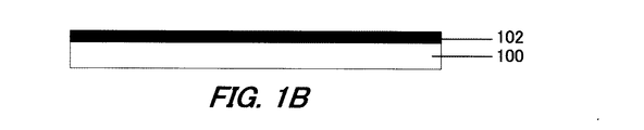
図1Aを参照すると、パターニングされる半導体基板100が示されている。典型的な例では、半導体基板100は一部に集積回路が形成されたシリコンウエハである。
Referring to FIG. 1A, a
図1Bは、半導体基板100に堆積したパターニング剤に敏感な金属含有膜102を示す。金属含有膜が母材に分解されるかその後の現像処理に敏感になるように、金属含有膜は、パターニング剤への露出に敏感な金属塩(例えば、メタルハライド)または有機金属化合物であってよい。適したパターニング剤は、光子、電子、陽子、イオン、または中性種であってよく、金属含有膜102が母材に分解されてそれらの種の1つにさらされることでパターニングされるか、またはその後の現像処理に敏感になるようにする。以下にさらに説明するように、有効な金属およびパターニング剤の組み合わせの特例は、メタルハライド(例えばSnBr4)または有機金属(例えばSn(CH3)4)として堆積されEUVリソグラフィでパターニングされるSnである。一般に、半導体基板100は、堆積の前に真空下で金属含有膜堆積のためにリアクタチャンバに設置される。
FIG. 1B shows a metal-containing
金属含有膜102のブランケットは、(例えば、ラムリサーチ(カリフォルニア州Fremount)から入手可能なAltus(登録商標)CVDツールのような非プラズマCVDリアクタにおいて)適した前駆体からの凝結によって形成されうる。例えば、臭化スズ(SnBr4)は、760Torrで205℃の標準沸点および31℃の融点を有し、10℃で10Torrの蒸気圧を有する。臭化スズは基板上に凝結して、露出時間および基板温度に依存する厚さ(例えば約5から200nm、例えば10nm)を有する固体SnBr4膜を形成しうる。凝結によるこの堆積に適した工程条件は、約0から30℃の間の堆積温度(例えば、約20℃)と、20Torr以下のリアクタ圧力(例えば、20℃で14から15Torrの間に維持された圧力)を含む。前駆体流速を約100から1000sccmの間に維持することで、堆積速度を制御することができる。
The blanket of metal-containing
Sn金属の代替源は有機金属であってよい。例えば、テトラメチルスズ(Sn(CH3)4)は、760Torrで75℃の標準沸点および−54℃の融点を有する。テトラメチルスズも基板上に凝結して、露出時間および基板温度に依存する厚さ(例えば約5から200Å、例えば100Å)を有する固体Sn(CH3)4膜を形成しうる。凝結によるこの堆積に適した工程条件は、約−54℃から30℃の間の堆積温度(例えば、約20℃)と、20Torr以下のリアクタ圧力(例えば、20℃で約1Torrに維持された圧力)を含む。前駆体流速を約100から1000sccmの間に維持することで、堆積速度を制御することができる。 An alternative source of Sn metal may be an organometal. For example, tetramethyltin (Sn (CH 3 ) 4 ) has a normal boiling point of 75 ° C. and a melting point of −54 ° C. at 760 Torr. Tetramethyltin can also condense on the substrate to form a solid Sn (CH 3 ) 4 film having a thickness that depends on the exposure time and substrate temperature (eg, about 5 to 200 mm, such as 100 mm). Suitable process conditions for this deposition by condensation include a deposition temperature between about -54 ° C. to 30 ° C. (eg, about 20 ° C.) and a reactor pressure of 20 Torr or less (eg, a pressure maintained at about 1 Torr at 20 ° C.). )including. By maintaining the precursor flow rate between about 100 and 1000 sccm, the deposition rate can be controlled.
金属マスクの形成に適した別の金属はハフニウム(Hf)である。塩化ハフニウム(HfCl4)(432℃の融点を有し、190℃で1Torrの蒸気圧)は基板上に凝結して、露出時間および基板温度に依存する厚さ(例えば約50から2000nm、例えば1000nm)を有する固体HfCl4結晶膜を形成しうる。凝結によるこの堆積に適した工程条件は、約0℃から300℃の間の堆積温度(例えば、約100℃)と、10Torr以下のリアクタ圧力(例えば、100℃で0.1から1Torrの間に維持された圧力)を含む。前駆体流速を約10から100sccmの間に維持することで、堆積速度を制御することができる。 Another metal suitable for forming a metal mask is hafnium (Hf). Hafnium chloride (HfCl 4 ) (having a melting point of 432 ° C. and a vapor pressure of 1 Torr at 190 ° C.) condenses on the substrate to a thickness that depends on the exposure time and the substrate temperature (eg about 50 to 2000 nm, eg 1000 nm ) Having a solid HfCl 4 crystal film. Process conditions suitable for this deposition by condensation include deposition temperatures between about 0 ° C. and 300 ° C. (eg, about 100 ° C.) and reactor pressures of 10 Torr or less (eg, between 0.1 and 1 Torr at 100 ° C. Maintained pressure). By maintaining the precursor flow rate between about 10 and 100 sccm, the deposition rate can be controlled.
水蒸気による変質を防ぐために、SnおよびHf含有膜の形成および搬送は真空環境で行われる。形成された膜は、その後EUVパターニングツールに搬送され、図1C−Dに示すように、フォトレジストを用いずに直接露光によってパターニングされる。 In order to prevent alteration due to water vapor, the formation and transport of the Sn and Hf-containing film are performed in a vacuum environment. The formed film is then transferred to an EUV patterning tool and patterned by direct exposure without using a photoresist, as shown in FIGS. 1C-D.
EUVLツールは、一般に堆積ツールよりも高真空で動作することに注意すべきである。この場合、堆積からパターニングツールへの搬送時に基板の真空環境を高め、パターニングツールへの搬入前に基板および堆積した金属含有膜を脱ガスすることが望ましい。これは、パターニングツールの光学系が基板の脱ガスによって汚染されないためである。 It should be noted that EUVL tools generally operate at a higher vacuum than deposition tools. In this case, it is desirable to increase the vacuum environment of the substrate during transfer from deposition to the patterning tool, and degas the substrate and the deposited metal-containing film before loading into the patterning tool. This is because the optical system of the patterning tool is not contaminated by degassing the substrate.
図1Cを参照すると、メタルハライドSn系金属含有膜はEUVLによってパターニングされ、分解化学現象は以下によって進行する:
SnBr4→Sn+2Br2
光子は、SnBr4をSn(スズ地金)および臭素ガス(Br2)に直接分解する。あるいは、反応物質X2(例えば、XがCl、I、またはHの場合)は反応経路SnBr4+X2→SnX4+2Br2を促進し、最終的には、特にSnX4が凝結しやすいSnBr4より簡単に光活性化する場合に、光分解によってSnにするために用いられうる。いずれの場合も、副生成物(Br2)および反応物質(X2)は、真空のような封じ込めが必要である。
Referring to FIG. 1C, the metal halide Sn-based metal-containing film is patterned by EUVL, and the decomposition chemistry proceeds as follows:
SnBr 4 → Sn + 2Br 2
Photons decompose SnBr 4 directly into Sn (tin metal) and bromine gas (Br 2 ). Alternatively, the reactant X 2 (e.g., X is Cl, I or, in the case of H,) promotes the reaction path SnBr 4 + X 2 → SnX 4 + 2Br 2, ultimately, SnBr 4, particularly SnX 4 tends to condense When more easily photoactivated, it can be used to Sn by photolysis. In either case, the by-product (Br 2 ) and the reactant (X 2 ) need to be sealed like a vacuum.
EUVLによってパターニングされた有機Sn系金属含有膜のために、光子はSn(CH3)4をSn(スズ地金)およびエタンガスに直接分解する。分解化学現象は以下によって進行する:
Sn(CH3)4→Sn+2C2H6
For an organic Sn-based metal-containing film patterned by EUVL, photons decompose Sn (CH3) 4 directly into Sn (tin metal) and ethane gas. Decomposition chemistry proceeds by:
Sn (CH 3 ) 4 → Sn + 2C 2 H 6
EUVLによってパターニングされたメタルハライドHf系金属含有膜のために、分解化学現象は以下によって進行する:
HfCl4→Hf+2Cl2
光子は、HfCl4をHf金属および塩素ガス(Cl2)に直接分解する。あるいは、反応物質X2(例えば、XがBr、I、またはHの場合)は反応経路HfCl4+X2→HfX4+2Cl2を促進し、最終的には、特にHfX4が凝結しやすいHfCl4より簡単に光活性化する場合に、光分解によってHfにするために用いられうる。いずれの場合も、副生成物(Cl2)および反応物質(X2)は、真空のような封じ込めが必要である。
For a metal halide Hf-based metal-containing film patterned by EUVL, the decomposition chemistry proceeds by:
HfCl 4 → Hf + 2Cl 2
Photons decompose HfCl 4 directly into Hf metal and chlorine gas (Cl 2 ). Alternatively, the reactant X 2 (e.g., X is Br, I or a H,) promotes the reaction path HfCl 4 + X 2 → HfX 4 + 2Cl 2, ultimately, HfCl 4, particularly HFX 4 tends to condense It can be used to make Hf by photolysis when more easily photoactivated. In either case, the by-product (Cl 2 ) and the reactant (X 2 ) need to be sealed like a vacuum.
図1Cに示すのは、形成された金属マスク102aの露光された金属含有膜領域およびパターン現像によって除去される材料の非露光領域102bのパターニング結果である。
FIG. 1C shows the patterning result of the exposed metal-containing film region of the formed
図1Dを参照すると、パターンはその後現像されうる。パターンの現像は、露光領域102aのみが完全に形成された金属マスクとして残るように、単に基板を加熱して金属含有膜の非露光領域102bを揮発することで生じうる。このパターン現像操作は、熱的および環境的に安定したパターン化金属マスクが形成されるため、真空統合を必要としなくともよいことに注意すべきである。また、金属含有膜分解の副生成物によるパターニングツールの光学系の汚染を避けるため、パターン現像はツールの外で行われることが望ましい。
Referring to FIG. 1D, the pattern can then be developed. Pattern development can occur by simply heating the substrate to volatilize the
図1Eを参照すると、任意の工程としてパターンの増幅が行われうる。例えば、選択性ALDまたは無電解堆積(ELD)は、さらに選択的に堆積した金属106によって金属マスクの厚みを増すために、図1Cおよび/または1Dに示す操作に次いでパターン化された基板上で実施されてよい。これは、マスクの光透過を低減するまたは機械的により頑強にするのに役立つかもしれない。かかる増幅は、例えば、米国特許第6,911,067号、第6,794,288号、第6,902,605号、および第4,935,312号に記載されているような無電解堆積処理を適用することで達成されてよい。これら全ての文献の開示内容全体は、参考として本願で援用される。
Referring to FIG. 1E, pattern amplification may be performed as an optional step. For example, selective ALD or electroless deposition (ELD) may be performed on a patterned substrate subsequent to the operations shown in FIGS. 1C and / or 1D to further increase the thickness of the metal mask by selectively deposited
例えば、この方法で初期の1nmシードは10nmに増幅されうる。図1Dを参照して説明したパターン現像のように、増幅前に熱的および環境的に安定したパターン化金属マスクが形成されるため、この操作は真空統合を必要としなくともよい。 For example, the initial 1 nm seed can be amplified to 10 nm in this manner. As with the pattern development described with reference to FIG. 1D, this operation may not require vacuum integration because a thermally and environmentally stable patterned metal mask is formed prior to amplification.
他の処理実施形態
金属塩または有機金属系金属含有膜堆積の別の方法として、金属含有EUV感応膜は、(例えば、いずれもラムリサーチ(カリフォルニア州Fremount)から入手可能なAltus(登録商標)CVDツールのような非プラズマCVDリアクタ、またはVector(登録商標)PECVDツールのようなPECVDリアクタにおいて)適した前駆体を用いた有機金属CVDの多段階処理によって堆積されうる。例えば、CH4/H2プラズマ堆積、それに続くアンモニア(NH3/H2)プラズマのような、アルキルおよびアミノ前駆体のプラズマ堆積は、半導体基板上にアミノプロピルトリエトキシシラン(APTES)のアミノ官能化自己組織化単層(SAM)を生成できる。かかるアミン末端の表面は、共形の無電解堆積(ELD)を可能にする。SAMはその後、EUVパターニングツールに搬送されてパターニングされうる。ELDによってパターン化されたSAMの選択的成長(例えば、これらのパラメータを与えられた当技術分野で公知の処理に従って、Pd触媒を提供するためのPdCl2/H2O溶液露光、それに続くNiまたはCoおよび銅(Cu)のELDによる)は、フォトレジストを用いずに形成された金属系マスクをもたらす。かかるSAMに基づくアプローチは、その目的で図1Eを参照に述べたELD技術の代替としてパターン増幅にも用いられうる。
Other Processing Embodiments As another method of metal salt or organometallic-based metal-containing film deposition, metal-containing EUV sensitive films (eg, Altus® CVD, both available from Lam Research, Fremount, Calif.). In a non-plasma CVD reactor such as a tool, or a PECVD reactor such as a Vector® PECVD tool) may be deposited by a multi-step process of metal organic CVD using a suitable precursor. For example, plasma deposition of alkyl and amino precursors, such as CH 4 / H 2 plasma deposition followed by ammonia (NH 3 / H 2 ) plasma, can be performed on aminopropyltriethoxysilane (APTES) amino functions on a semiconductor substrate. Self-assembled monolayer (SAM) can be generated. Such amine-terminated surfaces allow conformal electroless deposition (ELD). The SAM can then be transferred to an EUV patterning tool and patterned. Selective growth of SAM patterned by ELD (eg, PdCl 2 / H 2 O solution exposure to provide Pd catalyst according to processing known in the art given these parameters, followed by Ni or Co and copper (Cu) ELD) result in a metal-based mask formed without the use of a photoresist. Such a SAM-based approach can also be used for pattern amplification as an alternative to the ELD technique described with reference to FIG. 1E for that purpose.
本開示は本来、パターニング技術としてEUVLを参照しているが、他の実施形態は電子、イオン、または中間種の集束ビームを用いてブランケットマスク上にパターンを直接書くことができ、これらの工程も真空で実施されることにも注意すべきである。EUVLシステムの反射光学系上に副生成物が凝結する場合は、In−situのチャンバ洗浄が用いられてもよい。 Although this disclosure inherently refers to EUVL as a patterning technique, other embodiments can write patterns directly on a blanket mask using a focused beam of electrons, ions, or intermediate species, and these processes are also It should also be noted that it is carried out in a vacuum. In-situ chamber cleaning may be used if by-products condense on the reflective optics of the EUVL system.
装置
図3は、本明細書で述べる真空統合処理の実施に適した、真空搬送モジュールと連結する真空統合金属堆積およびパターニングモジュールを備えた半導体処理クラスタツールの構造を示す。ウエハを複数の収納設備および処理モジュールの間で「搬送」する搬送モジュールの配置は、「クラスタツール構造」システムと呼んでもよい。金属堆積およびパターニングモジュールは、特定処理の要件に従って真空統合される。真空搬送モジュール(VTM)338は、4つの処理モジュール320a−320dと連結し、個別に様々な製作処理を実施するために最適化されてよい。例として、処理モジュール320a−320dは、凝結、堆積、蒸発、ELD、エッチング、および/または他の半導体処理を実施するために実装されてよい。例えば、モジュール320aは、本明細書で述べる金属含有膜の堆積を行うのに適した、ラムリサーチ(カリフォルニア州Fremont)から入手可能なAltus(登録商標)CVDツールのような非プラズマCVDリアクタであってよい。そして、モジュール320bは、ラムリサーチのVector(登録商標)のようなPECVDツールであってよい。図は必ずしも正確な縮尺率ではないことに注意すべきである。
Apparatus FIG. 3 shows the structure of a semiconductor processing cluster tool with a vacuum integrated metal deposition and patterning module coupled to a vacuum transfer module, suitable for performing the vacuum integration process described herein. The arrangement of transfer modules that “transfer” wafers between a plurality of storage facilities and processing modules may be referred to as a “cluster tool structure” system. The metal deposition and patterning module is vacuum integrated according to the specific processing requirements. The vacuum transfer module (VTM) 338 may be coupled to the four
エアロック(別名ロードロックまたは搬送モジュール)342および346は、VTM338およびパターニングモジュール340と連結する。例えば、適したパターニングモジュールは、ASML社(オランダ、Veldhoven)によって提供されるTWINSCAN NXE:3300B(登録商標)プラットフォームであってよい。このツール構造によって、金属含有膜が堆積した基板のような工作物を露光前に反応しないように真空で搬送できる。EUVLがH2OやO2などの周囲ガスによる入射光子の強力な光吸収を伴う大幅な減圧も要求する事実によって、堆積モジュールとリソグラフィツールとの統合が容易になる。
Air locks (also known as load lock or transfer modules) 342 and 346 interface with
エアロック342は、堆積モジュール620aに仕えるVTM338からパターニングモジュール340への基板の搬送を指す「搬出」ロードロックであってよく、エアロック346は、パターニングモジュール340からVTM338への基板の搬送を指す「搬入」ロードロックであってよい。搬入ロードロック346はまた、基板のアクセスおよび撤去のためにツールの外側にインターフェースを備えてもよい。各処理モジュールは、VTM338とモジュールを連結するファセットを有する。例えば、堆積処理モジュール320aはファセット336を有する。各ファセット内では、ウエハ326が各装置間で移動する際にウエハの通過を感知するセンサ(図中のセンサ1−18)が用いられる。パターニングモジュール340、エアロック342および346は、図示されていない追加のファセットおよびセンサを同様に備えてよい。
主VTMロボット322は、エアロック342および346を含むモジュール間でウエハ326を搬送する。一実施形態では、ロボット322は1つのアームを有し、別の実施形態では、ロボット322は2つのアームを有する。各アームはエンドエフェクタ324を有し、移送のためにウエハ326のようなウエハを採取する。フロントエンドロボット344は、ウエハ326を搬出エアロック342からパターニングモジュール340へ、パターニングモジュール340から搬入エアロック346へ搬送するのに用いられる。フロントエンドロボット344はまた、搬入ロードロックと基板のアクセスおよび撤去用ツールの外側との間でウエハ326を移送してよい。搬入エアロックモジュール346は大気と真空との間の環境に調和させる能力を有するため、ウエハ326は損傷することなく2つの圧力環境の間を移動することができる。
EUVLツールは、一般に堆積ツールより高真空で作動することに注意すべきである。この場合、堆積からパターニングツールへの搬送時に基板の真空環境を高め、パターニングツールへの搬入前に基板および堆積した金属含有膜を脱ガスすることが望ましい。搬出エアロック342は、パターニングツール340の光学系が基板の脱ガスによって汚染されないように、オフガスの排出中は搬送されたウエハをパターニングモジュール340の圧力以下の低圧で保持することによってこの機能を提供してよい。搬出脱ガスエアロックに適した圧力は、1E−8Torr以下である。
It should be noted that EUVL tools generally operate at a higher vacuum than deposition tools. In this case, it is desirable to increase the vacuum environment of the substrate during transfer from deposition to the patterning tool, and degas the substrate and the deposited metal-containing film before loading into the patterning tool. The carry-out
いくつかの実施形態では、システム制御装置350(1つ以上の物理または論理制御装置を含んでよい)は、クラスタツールおよび/またはその別体のモジュールのいくつかまたは全ての作動を制御する。制御装置は、クラスタ構造にローカルとなりうるか、製造現場または遠隔位置においてクラスタ構造の外に設置されることができ、ネットワークでクラスタ構造に接続されうる。システム制御装置350は、1つ以上のメモリ装置および1つ以上のプロセッサを備えてよい。プロセッサは、中央処理装置(CPU)またはコンピュータ、アナログおよび/またはデジタル入出力接続部、ステッパモータ制御盤、および他の同様なコンポーネントを備えてよい。適切な制御操作を実施するための命令は、プロセッサで実行される。これらの命令は、制御装置と結合したメモリ装置に記憶されるか、ネットワークを通じて提供されてよい。特定の実施形態では、システム制御装置はシステム制御ソフトウェアを実行する。 In some embodiments, (which may include one or more physical or logical controller) system controller 3 50 controls some or all of the operating modules of the cluster tool and / or separate thereof. The controller can be local to the cluster structure or can be installed outside the cluster structure at the manufacturing site or at a remote location and can be connected to the cluster structure by a network. The system controller 3 50 may comprise one or more memory devices and one or more processors. The processor may comprise a central processing unit (CPU) or computer, analog and / or digital input / output connections, stepper motor control boards, and other similar components. Instructions for performing appropriate control operations are executed by the processor. These instructions may be stored in a memory device coupled to the controller or provided over a network. In certain embodiments, the system controller executes system control software.
システム制御ソフトウェアは、ツールまたはモジュール操作の任意の態様の適用タイミングおよび/または大きさを制御するための命令を含んでよい。システム制御ソフトウェアは、任意の適切な方法で構成されてよい。例えば、様々な処理ツールコンポーネントサブルーチンまたは制御対象は、様々な処理ツールの処理を実行するのに必要な処理ツールコンポーネントの制御操作に書き込まれてよい。システム制御ソフトウェアは、任意のコンピュータ可読プログラミング言語にコード化されてよい。いくつかの実施形態では、システム制御ソフトウェアは、上述された様々なパラメータを制御するための命令を配列する入出力制御(IOC)を含む。例えば、半導体製造方法の各フェーズは、システム制御装置による実行のための1つ以上の命令を含んでよい。凝結、堆積、蒸発、パターニング、および/またはエッチングフェーズの工程条件を設定する命令は、例えば対応する処方フェーズに含まれてよい。 The system control software may include instructions for controlling the application timing and / or magnitude of any aspect of tool or module operation. The system control software may be configured in any suitable manner. For example, various processing tool component subroutines or objects to be controlled may be written into the processing tool component control operations necessary to perform the processing of the various processing tools. The system control software may be encoded in any computer readable programming language. In some embodiments, the system control software includes an input / output control (IOC) that arranges instructions for controlling the various parameters described above. For example, each phase of the semiconductor manufacturing method may include one or more instructions for execution by the system controller. Instructions for setting process conditions for the condensation, deposition, evaporation, patterning, and / or etching phase may be included in the corresponding recipe phase, for example.
結論
本明細書で述べた膜堆積およびリソグラフィ工程の真空統合と装置は、EUV感応金属膜の堆積と、分解または変質を避けるために真空環境での直接EUV露光によるパターニングとを提供する。EUVLは、周囲ガスの光吸収による13.5nmの入射光束の変質を避けるため、真空で行われる。記述した真空統合ハードマスク処理の利点は:EUVシステムの真空操作は、酸素および湿度感受性のある化合物を用いる可能性を広げることと;装置において堆積システムとEUVシステムを真空統合することで、これらの材料の使用が可能になることである。金属前駆体の光分解は、光分解が金属膜の高い吸着によって強化された場合に非線形反応を作り出す。金属は、フォトレジストよりも高エネルギー二次電子の熱化に優れているため、コントラストまたはLERを改善する。金属膜を直接マスクとしてまたはパターン増幅して用いることで、はるかに薄い膜および要求される露光時間の削減が可能になる。金属膜はエッチングにとってより良いハードマスクとなり、マスクの視点から求められる厚みを減少させる。さらに、EUVの真空および光学系に適合する材料、金属堆積に適した用量閾値を有する有機金属前駆体、所定空間の核生成部位を除去するため複数の光分解事象を伴う核生成膜のさらなる開発および最適化が、本明細書に述べた処理に従って進められうる。
Conclusion The vacuum integration and apparatus of the film deposition and lithography processes described herein provides for the deposition of EUV sensitive metal films and patterning by direct EUV exposure in a vacuum environment to avoid degradation or alteration. EUVL is performed in vacuum to avoid alteration of the incident light flux of 13.5 nm due to light absorption of ambient gas. The advantages of the vacuum integrated hard mask process described are: The vacuum operation of the EUV system expands the possibility of using oxygen and humidity sensitive compounds; and by vacuum integrating the deposition system and the EUV system in the apparatus, these The material can be used. Photodegradation of metal precursors creates a non-linear reaction when photolysis is enhanced by high adsorption of the metal film. Metals are better at thermalizing high energy secondary electrons than photoresists and thus improve contrast or LER. By using a metal film directly as a mask or with pattern amplification, a much thinner film and the required exposure time can be reduced. The metal film becomes a better hard mask for etching and reduces the thickness required from the mask perspective. Further development of materials compatible with EUV vacuum and optics, organometallic precursors with dose thresholds suitable for metal deposition, and nucleation films with multiple photolysis events to remove nucleation sites in a given space And optimization can proceed according to the process described herein.
本明細書で述べた実施例および実施形態は例示であり、上述に照らした様々な修正または変更が当業者に示唆される。明瞭性のために様々な詳細が省略されたが、様々な設計の選択肢が実施されてよい。そのため、本実施例は例示であり、限定を意図するものではない。本発明は、本明細書に記載された詳細に限定されるものではなく、特許請求の範囲から逸脱することなく修正が可能である。
本発明は、以下の適用例としても実現できる。
[適用例1]
金属ハードマスクのフォトレジストレス形成方法であって、
半導体基板上にEUV感受性の金属含有膜を堆積させることと、
前記金属含有膜を真空環境で直接EUV露光することによってパターン化し、金属ハードマスクを形成することと、
を含む方法。
[適用例2]
適用例1に記載の方法であって、前記金属含有膜は金属塩である、方法。
[適用例3]
適用例2に記載の方法であって、前記金属塩はメタルハライドである、方法。
[適用例4]
適用例3に記載の方法であって、前記金属はスズ(Sn)である、方法。
[適用例5]
適用例3に記載の方法であって、前記金属はハフニウム(Hf)である、方法。
[適用例6]
適用例1に記載の方法であって、前記金属含有膜は有機金属化合物である、方法。
[適用例7]
適用例6に記載の方法であって、前記有機金属化合物の前記金属はスズ(Sn)である、方法。
[適用例8]
適用例1に記載の方法であって、前記半導体基板は、部分的に形成された集積回路を含むシリコンウエハであり、さらに、
前記堆積の前に、金属含有膜堆積のために前記半導体基板を第1のリアクタチャンバに供給することと、
堆積の後に、パターニングのために前記基板を真空下でリソグラフィ処理チャンバに搬送することと、
を含む方法。
[適用例9]
適用例8に記載の方法であって、さらに、前記リソグラフィ処理チャンバに入れる前に前記基板を脱ガスすることを含む、方法。
[適用例10]
適用例9に記載の方法であって、前記脱ガスは、前記基板の周囲の圧力を1E−8Torr以下に減少させることを含む、方法。
[適用例11]
適用例1に記載の方法であって、さらに、前記金属ハードマスク上への選択的堆積によるパターン増幅を含む、方法。
[適用例12]
適用例11に記載の方法であって、前記選択的堆積は無電解めっきを含む、方法。
[適用例13]
金属ハードマスクのフォトレジストレス形成方法であって、
半導体基板上に、光子、電子、陽子、イオン、または中性種を含むパターニング剤に敏感な金属含有膜を、前記膜がそれらの種の1つにさらされてパターンニングされるように、堆積させることと、
前記金属含有膜を真空環境で前記パターニング剤に直接さらしてパターニングすることと、
を含む方法。
[適用例14]
適用例13に記載の方法であって、前記金属含有膜は感光性があり、前記パターニングは光リソグラフィを用いて行われる、方法。
[適用例15]
適用例14に記載の方法であって、前記光リソグラフィはEUVリソグラフィである、方法。
[適用例16]
フォトレジストレス金属ハードマスク形成を行う装置であって、
金属含有膜堆積モジュールと、
金属含有膜パターニングモジュールと、
前記堆積モジュールと前記パターニングモジュールとを接続する真空搬送モジュールと、
を備える装置。
[適用例17]
適用例16に記載の装置であって、
前記堆積モジュールは、感光性メタルハライドまたは有機金属化合物膜を堆積させるリアクタチャンバを備え、
前記パターニングモジュールは、波長サブ30nmの放射源を有するフォトリソグラフィツールを備える、装置。
[適用例18]
適用例17に記載の装置であって、前記パターニングモジュールはEUVリソグラフィツールである、装置。
[適用例19]
適用例17に記載の装置であって、前記金属含有膜がパターニング剤にさらされてパターニングされるように、前記パターニングモジュールは、光子、電子、陽子、イオン、および中性種からなる群から選択されるパターニング剤源を有する、装置。
[適用例20]
適用例17に記載の装置であって、さらに、基板を前記パターニングモジュールから前記真空搬送モジュールに搬送するための搬入ロードロックと、基板を前記真空搬送モジュールから前記パターニングモジュールに搬送するための搬出ロードロックとを備え、前記搬出ロードロックは脱ガスモジュールとして機能する、装置。
[適用例21]
適用例17に記載の装置であって、さらに、フォトレジストレス金属ハードマスク形成を行うための命令を含む制御装置を備え、前記命令は、
前記金属含有膜堆積モジュールにおいて、半導体基板上にEUV感受性の金属含有膜を堆積させるためと、
前記基板を真空下で前記金属含有膜パターニングモジュールに搬送するためと、
前記金属含有膜パターニングモジュールにおいて、前記金属含有膜を真空環境で直接EUV露光することよってパターン化し、金属ハードマスクを形成するため
の命令を含む、装置。
The examples and embodiments described herein are exemplary and various modifications or changes in light of the above will be suggested to those skilled in the art. Although various details have been omitted for clarity, various design options may be implemented. For this reason, this example is illustrative and not intended to be limiting. The invention is not limited to the details described herein, but modifications can be made without departing from the scope of the claims.
The present invention can also be realized as the following application examples.
[Application Example 1]
A method for forming a metal hard mask without a photoresist,
Depositing an EUV sensitive metal-containing film on a semiconductor substrate;
Patterning the metal-containing film by direct EUV exposure in a vacuum environment to form a metal hard mask;
Including methods.
[Application Example 2]
The method according to application example 1, wherein the metal-containing film is a metal salt.
[Application Example 3]
The method according to application example 2, wherein the metal salt is a metal halide.
[Application Example 4]
The method according to application example 3, wherein the metal is tin (Sn).
[Application Example 5]
The method according to application example 3, wherein the metal is hafnium (Hf).
[Application Example 6]
The method according to application example 1, wherein the metal-containing film is an organometallic compound.
[Application Example 7]
The method according to application example 6, wherein the metal of the organometallic compound is tin (Sn).
[Application Example 8]
The method according to application example 1, wherein the semiconductor substrate is a silicon wafer including a partially formed integrated circuit, and
Supplying the semiconductor substrate to a first reactor chamber for metal-containing film deposition prior to the deposition;
After deposition, transporting the substrate under vacuum to a lithographic processing chamber for patterning;
Including methods.
[Application Example 9]
The method of application 8, further comprising degassing the substrate prior to entering the lithographic processing chamber.
[Application Example 10]
The method of application example 9, wherein the degassing includes reducing the pressure around the substrate to 1E-8 Torr or less.
[Application Example 11]
The method of application example 1, further comprising pattern amplification by selective deposition on the metal hard mask.
[Application Example 12]
The method according to application example 11, wherein the selective deposition includes electroless plating.
[Application Example 13]
A method for forming a metal hard mask without a photoresist,
Depositing a metal-containing film sensitive to a patterning agent containing photons, electrons, protons, ions, or neutral species on a semiconductor substrate such that the film is patterned by exposure to one of those species And letting
Patterning the metal-containing film by direct exposure to the patterning agent in a vacuum environment;
Including methods.
[Application Example 14]
14. The method according to application example 13, wherein the metal-containing film is photosensitive and the patterning is performed using photolithography.
[Application Example 15]
The method according to application example 14, wherein the optical lithography is EUV lithography.
[Application Example 16]
An apparatus for forming a photoresist-less metal hard mask,
A metal-containing film deposition module;
A metal-containing film patterning module;
A vacuum transfer module connecting the deposition module and the patterning module;
A device comprising:
[Application Example 17]
The apparatus according to application example 16,
The deposition module comprises a reactor chamber for depositing a photosensitive metal halide or organometallic compound film,
The patterning module comprises a photolithography tool having a radiation source with a wavelength sub-30 nm.
[Application Example 18]
The apparatus according to application example 17, wherein the patterning module is an EUV lithography tool.
[Application Example 19]
The apparatus according to application example 17, wherein the patterning module is selected from the group consisting of photons, electrons, protons, ions, and neutral species so that the metal-containing film is patterned by exposure to a patterning agent. An apparatus having a source of patterning agent.
[Application Example 20]
18. The apparatus according to application example 17, further including a loading load lock for transporting a substrate from the patterning module to the vacuum transport module, and an unloading load for transporting the substrate from the vacuum transport module to the patterning module. And an unloading load lock functioning as a degassing module.
[Application Example 21]
The apparatus according to application example 17, further comprising a control device including a command for performing a photoresist-less metal hard mask formation, wherein the command includes:
In the metal-containing film deposition module, for depositing an EUV-sensitive metal-containing film on a semiconductor substrate;
For transporting the substrate to the metal-containing film patterning module under vacuum;
In the metal-containing film patterning module, the metal-containing film is patterned by direct EUV exposure in a vacuum environment to form a metal hard mask.
Equipment, including instructions.
Claims (21)
5〜200nmの厚みを有するSnBr 4 、5〜200Åの厚みを有するSn(CH 3 ) 4 、および、50〜2000nmの厚みを有する結晶性HfCl 4 、からなる群から選択される膜を有するEUV感受性の金属含有膜を凝結により半導体基板上に堆積させることと、
前記金属含有膜を真空環境で直接、10〜20nmの範囲内の波長を有するEUV露光によって30nm未満の分解能でパターン化すること、および、
前記パターンを現像して前記金属マスクを形成することと、
を含む方法。 A photo resistless method of forming a gold Shokuma disk,
EUV sensitivity having a film selected from the group consisting of SnBr 4 having a thickness of 5 to 200 nm, Sn (CH 3 ) 4 having a thickness of 5 to 200 mm , and crystalline HfCl 4 having a thickness of 50 to 2000 nm. Depositing a metal-containing film on a semiconductor substrate by condensation ;
The metal-containing film directly in a vacuum environment, be patterned with a resolution of thus less than 30nm in EUV exposure light having a wavelength in the range of: 10 to 20 nm, and,
Developing the pattern to form the metal mask;
Including methods.
前記堆積の前に、金属含有膜堆積のために前記半導体基板を第1のリアクタチャンバに供給することと、
堆積の後に、パターニングのために前記基板を真空下でリソグラフィ処理チャンバに搬送することと、
を含む方法。 The method of claim 1, wherein the semiconductor substrate is a silicon wafer including a partially formed integrated circuit, and
Supplying the semiconductor substrate to a first reactor chamber for metal-containing film deposition prior to the deposition;
After deposition, transporting the substrate under vacuum to a lithographic processing chamber for patterning;
Including methods.
5〜200nmの厚みを有するSnBr 4 、5〜200Åの厚みを有するSn(CH 3 ) 4 、および、50〜2000nmの厚みを有する結晶性HfCl 4 、からなる群から選択される膜を有するEUV感受性の金属含有膜を凝結により半導体基板上に堆積させるように構成された金属含有膜堆積モジュールと、
前記金属含有膜を真空環境で直接、10〜20nmの範囲内の波長を有するEUV露光によって30nm未満の分解能でパターン化するように構成された金属含有膜パターニングモジュールと、
前記堆積モジュールと前記パターニングモジュールとを接続する真空搬送モジュールと、
を備える装置。 An apparatus for performing photo resistless gold Shokuma disk form,
EUV sensitivity having a film selected from the group consisting of SnBr 4 having a thickness of 5 to 200 nm, Sn (CH 3 ) 4 having a thickness of 5 to 200 mm , and crystalline HfCl 4 having a thickness of 50 to 2000 nm. A metal-containing film deposition module configured to deposit a metal-containing film on a semiconductor substrate by condensation ;
A metal-containing film patterning module configured to pattern the metal-containing film directly in a vacuum environment by EUV exposure having a wavelength in the range of 10-20 nm with a resolution of less than 30 nm ;
A vacuum transfer module connecting the deposition module and the patterning module;
A device comprising:
前記堆積モジュールは、前記EUV感受性の金属含有膜を堆積させるリアクタチャンバを備え、
前記パターニングモジュールは、前記30nm未満の波長の放射源を有するフォトリソグラフィツールを備える、装置。 The apparatus of claim 16, comprising:
The deposition module comprises a reactor chamber for depositing the EUV sensitive metal-containing film;
The patterning module comprises a photolithography tool having a radiation source with a wavelength of less than the 30 nm, device.
前記金属含有膜堆積モジュールにおいて、半導体基板上に前記EUV感受性の金属含有膜を堆積させるため、
前記基板を真空下で前記金属含有膜パターニングモジュールに搬送するため、
前記金属含有膜パターニングモジュールにおいて、前記金属含有膜を真空環境で直接EUV露光することよってパターン化するため、および、
前記パターンを現像して前記金属マスクを形成するため、
の命令を含む、装置。 The apparatus of claim 17, further comprising a controller including instructions for performing the photo resistless gold Shokuma disk formation, the instructions comprising:
In the metal-containing film deposition module, because said depositing a metal-containing film of the EUV sensitive on a semiconductor substrate,
Order to convey the substrate to the metal-containing film patterning module under vacuum,
In the metal-containing film patterning module, for patterning the metal-containing film by direct EUV exposure in a vacuum environment , and
In order to form the metal mask by developing the pattern ,
Equipment, including instructions.
Applications Claiming Priority (2)
| Application Number | Priority Date | Filing Date | Title |
|---|---|---|---|
| US201461934514P | 2014-01-31 | 2014-01-31 | |
| US61/934,514 | 2014-01-31 |
Publications (3)
| Publication Number | Publication Date |
|---|---|
| JP2015201622A JP2015201622A (en) | 2015-11-12 |
| JP2015201622A5 JP2015201622A5 (en) | 2018-03-15 |
| JP6495025B2 true JP6495025B2 (en) | 2019-04-03 |
Family
ID=53755444
Family Applications (1)
| Application Number | Title | Priority Date | Filing Date |
|---|---|---|---|
| JP2015016254A Active JP6495025B2 (en) | 2014-01-31 | 2015-01-30 | Vacuum integrated hard mask processing and equipment |
Country Status (5)
| Country | Link |
|---|---|
| US (7) | US9778561B2 (en) |
| JP (1) | JP6495025B2 (en) |
| KR (1) | KR102306612B1 (en) |
| CN (2) | CN105047541B (en) |
| TW (1) | TWI639179B (en) |
Families Citing this family (270)
| Publication number | Priority date | Publication date | Assignee | Title |
|---|---|---|---|---|
| US9394608B2 (en) | 2009-04-06 | 2016-07-19 | Asm America, Inc. | Semiconductor processing reactor and components thereof |
| US8802201B2 (en) | 2009-08-14 | 2014-08-12 | Asm America, Inc. | Systems and methods for thin-film deposition of metal oxides using excited nitrogen-oxygen species |
| US9176377B2 (en) | 2010-06-01 | 2015-11-03 | Inpria Corporation | Patterned inorganic layers, radiation based patterning compositions and corresponding methods |
| US20130023129A1 (en) | 2011-07-20 | 2013-01-24 | Asm America, Inc. | Pressure transmitter for a semiconductor processing environment |
| US9017481B1 (en) | 2011-10-28 | 2015-04-28 | Asm America, Inc. | Process feed management for semiconductor substrate processing |
| US10714315B2 (en) | 2012-10-12 | 2020-07-14 | Asm Ip Holdings B.V. | Semiconductor reaction chamber showerhead |
| US20160376700A1 (en) | 2013-02-01 | 2016-12-29 | Asm Ip Holding B.V. | System for treatment of deposition reactor |
| KR102306612B1 (en) | 2014-01-31 | 2021-09-29 | 램 리써치 코포레이션 | Vacuum-integrated hardmask processes and apparatus |
| US11015245B2 (en) | 2014-03-19 | 2021-05-25 | Asm Ip Holding B.V. | Gas-phase reactor and system having exhaust plenum and components thereof |
| US10858737B2 (en) | 2014-07-28 | 2020-12-08 | Asm Ip Holding B.V. | Showerhead assembly and components thereof |
| US9890456B2 (en) | 2014-08-21 | 2018-02-13 | Asm Ip Holding B.V. | Method and system for in situ formation of gas-phase compounds |
| US10941490B2 (en) | 2014-10-07 | 2021-03-09 | Asm Ip Holding B.V. | Multiple temperature range susceptor, assembly, reactor and system including the susceptor, and methods of using the same |
| KR20230156842A (en) * | 2014-10-23 | 2023-11-14 | 인프리아 코포레이션 | Organometallic solution based high resolution patterning compositions and corresponding methods |
| US10276355B2 (en) | 2015-03-12 | 2019-04-30 | Asm Ip Holding B.V. | Multi-zone reactor, system including the reactor, and method of using the same |
| US10458018B2 (en) | 2015-06-26 | 2019-10-29 | Asm Ip Holding B.V. | Structures including metal carbide material, devices including the structures, and methods of forming same |
| CN108351594B (en) | 2015-10-13 | 2021-07-09 | 因普里亚公司 | Organotin oxide hydroxide patterning compositions, precursors, and patterning |
| US10211308B2 (en) | 2015-10-21 | 2019-02-19 | Asm Ip Holding B.V. | NbMC layers |
| US9996004B2 (en) * | 2015-11-20 | 2018-06-12 | Lam Research Corporation | EUV photopatterning of vapor-deposited metal oxide-containing hardmasks |
| US11139308B2 (en) | 2015-12-29 | 2021-10-05 | Asm Ip Holding B.V. | Atomic layer deposition of III-V compounds to form V-NAND devices |
| US10529554B2 (en) | 2016-02-19 | 2020-01-07 | Asm Ip Holding B.V. | Method for forming silicon nitride film selectively on sidewalls or flat surfaces of trenches |
| JP6762831B2 (en) * | 2016-03-31 | 2020-09-30 | 東京エレクトロン株式会社 | Hardmask forming method, hardmask forming device and storage medium |
| US10224202B2 (en) * | 2016-03-31 | 2019-03-05 | Tokyo Electron Limited | Forming method of hard mask, forming apparatus of hard mask and recording medium |
| US10190213B2 (en) | 2016-04-21 | 2019-01-29 | Asm Ip Holding B.V. | Deposition of metal borides |
| US10865475B2 (en) | 2016-04-21 | 2020-12-15 | Asm Ip Holding B.V. | Deposition of metal borides and silicides |
| US10367080B2 (en) | 2016-05-02 | 2019-07-30 | Asm Ip Holding B.V. | Method of forming a germanium oxynitride film |
| US11453943B2 (en) | 2016-05-25 | 2022-09-27 | Asm Ip Holding B.V. | Method for forming carbon-containing silicon/metal oxide or nitride film by ALD using silicon precursor and hydrocarbon precursor |
| US9859127B1 (en) * | 2016-06-10 | 2018-01-02 | Lam Research Corporation | Line edge roughness improvement with photon-assisted plasma process |
| US10612137B2 (en) | 2016-07-08 | 2020-04-07 | Asm Ip Holdings B.V. | Organic reactants for atomic layer deposition |
| US9859151B1 (en) | 2016-07-08 | 2018-01-02 | Asm Ip Holding B.V. | Selective film deposition method to form air gaps |
| US9812320B1 (en) | 2016-07-28 | 2017-11-07 | Asm Ip Holding B.V. | Method and apparatus for filling a gap |
| US9887082B1 (en) | 2016-07-28 | 2018-02-06 | Asm Ip Holding B.V. | Method and apparatus for filling a gap |
| KR102532607B1 (en) | 2016-07-28 | 2023-05-15 | 에이에스엠 아이피 홀딩 비.브이. | Substrate processing apparatus and method of operating the same |
| US10622211B2 (en) * | 2016-08-05 | 2020-04-14 | Taiwan Semiconductor Manufacturing Co., Ltd. | Metal-compound-removing solvent and method in lithography |
| US10643826B2 (en) | 2016-10-26 | 2020-05-05 | Asm Ip Holdings B.V. | Methods for thermally calibrating reaction chambers |
| US11532757B2 (en) | 2016-10-27 | 2022-12-20 | Asm Ip Holding B.V. | Deposition of charge trapping layers |
| US10229833B2 (en) | 2016-11-01 | 2019-03-12 | Asm Ip Holding B.V. | Methods for forming a transition metal nitride film on a substrate by atomic layer deposition and related semiconductor device structures |
| US10714350B2 (en) | 2016-11-01 | 2020-07-14 | ASM IP Holdings, B.V. | Methods for forming a transition metal niobium nitride film on a substrate by atomic layer deposition and related semiconductor device structures |
| KR20190071833A (en) * | 2016-11-13 | 2019-06-24 | 어플라이드 머티어리얼스, 인코포레이티드 | Surface treatment for EUV lithography |
| CN106444934B (en) * | 2016-11-14 | 2019-02-19 | 北京北方华创微电子装备有限公司 | A kind of process control system dispatching device and method based on condition managing |
| KR102546317B1 (en) | 2016-11-15 | 2023-06-21 | 에이에스엠 아이피 홀딩 비.브이. | Gas supply unit and substrate processing apparatus including the same |
| KR20180068582A (en) | 2016-12-14 | 2018-06-22 | 에이에스엠 아이피 홀딩 비.브이. | Substrate processing apparatus |
| US11447861B2 (en) | 2016-12-15 | 2022-09-20 | Asm Ip Holding B.V. | Sequential infiltration synthesis apparatus and a method of forming a patterned structure |
| US11581186B2 (en) | 2016-12-15 | 2023-02-14 | Asm Ip Holding B.V. | Sequential infiltration synthesis apparatus |
| KR20180070971A (en) | 2016-12-19 | 2018-06-27 | 에이에스엠 아이피 홀딩 비.브이. | Substrate processing apparatus |
| US10269558B2 (en) | 2016-12-22 | 2019-04-23 | Asm Ip Holding B.V. | Method of forming a structure on a substrate |
| US10867788B2 (en) | 2016-12-28 | 2020-12-15 | Asm Ip Holding B.V. | Method of forming a structure on a substrate |
| US11390950B2 (en) | 2017-01-10 | 2022-07-19 | Asm Ip Holding B.V. | Reactor system and method to reduce residue buildup during a film deposition process |
| US10468261B2 (en) | 2017-02-15 | 2019-11-05 | Asm Ip Holding B.V. | Methods for forming a metallic film on a substrate by cyclical deposition and related semiconductor device structures |
| US10163633B2 (en) * | 2017-03-13 | 2018-12-25 | Globalfoundries Inc. | Non-mandrel cut formation |
| US10529563B2 (en) | 2017-03-29 | 2020-01-07 | Asm Ip Holdings B.V. | Method for forming doped metal oxide films on a substrate by cyclical deposition and related semiconductor device structures |
| KR102457289B1 (en) | 2017-04-25 | 2022-10-21 | 에이에스엠 아이피 홀딩 비.브이. | Method for depositing a thin film and manufacturing a semiconductor device |
| US10770286B2 (en) | 2017-05-08 | 2020-09-08 | Asm Ip Holdings B.V. | Methods for selectively forming a silicon nitride film on a substrate and related semiconductor device structures |
| US10892156B2 (en) | 2017-05-08 | 2021-01-12 | Asm Ip Holding B.V. | Methods for forming a silicon nitride film on a substrate and related semiconductor device structures |
| US10796912B2 (en) | 2017-05-16 | 2020-10-06 | Lam Research Corporation | Eliminating yield impact of stochastics in lithography |
| US10199270B2 (en) * | 2017-05-25 | 2019-02-05 | Globalfoundries Inc. | Multi-directional self-aligned multiple patterning |
| US10886123B2 (en) | 2017-06-02 | 2021-01-05 | Asm Ip Holding B.V. | Methods for forming low temperature semiconductor layers and related semiconductor device structures |
| US11306395B2 (en) | 2017-06-28 | 2022-04-19 | Asm Ip Holding B.V. | Methods for depositing a transition metal nitride film on a substrate by atomic layer deposition and related deposition apparatus |
| CN107365958B (en) * | 2017-07-13 | 2020-01-07 | 上海天马有机发光显示技术有限公司 | Preparation method of metal mask plate |
| KR20190009245A (en) | 2017-07-18 | 2019-01-28 | 에이에스엠 아이피 홀딩 비.브이. | Methods for forming a semiconductor device structure and related semiconductor device structures |
| US10541333B2 (en) | 2017-07-19 | 2020-01-21 | Asm Ip Holding B.V. | Method for depositing a group IV semiconductor and related semiconductor device structures |
| US11374112B2 (en) | 2017-07-19 | 2022-06-28 | Asm Ip Holding B.V. | Method for depositing a group IV semiconductor and related semiconductor device structures |
| US11018002B2 (en) | 2017-07-19 | 2021-05-25 | Asm Ip Holding B.V. | Method for selectively depositing a Group IV semiconductor and related semiconductor device structures |
| US10590535B2 (en) | 2017-07-26 | 2020-03-17 | Asm Ip Holdings B.V. | Chemical treatment, deposition and/or infiltration apparatus and method for using the same |
| US10770336B2 (en) | 2017-08-08 | 2020-09-08 | Asm Ip Holding B.V. | Substrate lift mechanism and reactor including same |
| US10692741B2 (en) | 2017-08-08 | 2020-06-23 | Asm Ip Holdings B.V. | Radiation shield |
| US11139191B2 (en) | 2017-08-09 | 2021-10-05 | Asm Ip Holding B.V. | Storage apparatus for storing cassettes for substrates and processing apparatus equipped therewith |
| US11769682B2 (en) | 2017-08-09 | 2023-09-26 | Asm Ip Holding B.V. | Storage apparatus for storing cassettes for substrates and processing apparatus equipped therewith |
| US11830730B2 (en) | 2017-08-29 | 2023-11-28 | Asm Ip Holding B.V. | Layer forming method and apparatus |
| US11295980B2 (en) | 2017-08-30 | 2022-04-05 | Asm Ip Holding B.V. | Methods for depositing a molybdenum metal film over a dielectric surface of a substrate by a cyclical deposition process and related semiconductor device structures |
| KR102491945B1 (en) | 2017-08-30 | 2023-01-26 | 에이에스엠 아이피 홀딩 비.브이. | Substrate processing apparatus |
| US11056344B2 (en) | 2017-08-30 | 2021-07-06 | Asm Ip Holding B.V. | Layer forming method |
| KR102630301B1 (en) | 2017-09-21 | 2024-01-29 | 에이에스엠 아이피 홀딩 비.브이. | Method of sequential infiltration synthesis treatment of infiltrateable material and structures and devices formed using same |
| US10844484B2 (en) | 2017-09-22 | 2020-11-24 | Asm Ip Holding B.V. | Apparatus for dispensing a vapor phase reactant to a reaction chamber and related methods |
| US10658205B2 (en) | 2017-09-28 | 2020-05-19 | Asm Ip Holdings B.V. | Chemical dispensing apparatus and methods for dispensing a chemical to a reaction chamber |
| US10403504B2 (en) | 2017-10-05 | 2019-09-03 | Asm Ip Holding B.V. | Method for selectively depositing a metallic film on a substrate |
| US10923344B2 (en) | 2017-10-30 | 2021-02-16 | Asm Ip Holding B.V. | Methods for forming a semiconductor structure and related semiconductor structures |
| US10910262B2 (en) | 2017-11-16 | 2021-02-02 | Asm Ip Holding B.V. | Method of selectively depositing a capping layer structure on a semiconductor device structure |
| US11022879B2 (en) | 2017-11-24 | 2021-06-01 | Asm Ip Holding B.V. | Method of forming an enhanced unexposed photoresist layer |
| TWI791689B (en) | 2017-11-27 | 2023-02-11 | 荷蘭商Asm智慧財產控股私人有限公司 | Apparatus including a clean mini environment |
| JP7214724B2 (en) | 2017-11-27 | 2023-01-30 | エーエスエム アイピー ホールディング ビー.ブイ. | Storage device for storing wafer cassettes used in batch furnaces |
| KR102374206B1 (en) | 2017-12-05 | 2022-03-14 | 삼성전자주식회사 | Method of fabricating semiconductor device |
| EP3503164A1 (en) * | 2017-12-21 | 2019-06-26 | IMEC vzw | Selective deposition of metal-organic frameworks |
| US10109517B1 (en) | 2018-01-10 | 2018-10-23 | Lam Research Corporation | Rotational indexer with additional rotational axes |
| US10872771B2 (en) | 2018-01-16 | 2020-12-22 | Asm Ip Holding B. V. | Method for depositing a material film on a substrate within a reaction chamber by a cyclical deposition process and related device structures |
| TW202325889A (en) | 2018-01-19 | 2023-07-01 | 荷蘭商Asm 智慧財產控股公司 | Deposition method |
| CN111630203A (en) | 2018-01-19 | 2020-09-04 | Asm Ip私人控股有限公司 | Method for depositing gap filling layer by plasma auxiliary deposition |
| US11018047B2 (en) | 2018-01-25 | 2021-05-25 | Asm Ip Holding B.V. | Hybrid lift pin |
| USD880437S1 (en) | 2018-02-01 | 2020-04-07 | Asm Ip Holding B.V. | Gas supply plate for semiconductor manufacturing apparatus |
| US11081345B2 (en) | 2018-02-06 | 2021-08-03 | Asm Ip Holding B.V. | Method of post-deposition treatment for silicon oxide film |
| US10896820B2 (en) | 2018-02-14 | 2021-01-19 | Asm Ip Holding B.V. | Method for depositing a ruthenium-containing film on a substrate by a cyclical deposition process |
| JP7124098B2 (en) | 2018-02-14 | 2022-08-23 | エーエスエム・アイピー・ホールディング・ベー・フェー | Method for depositing a ruthenium-containing film on a substrate by a cyclical deposition process |
| KR102636427B1 (en) | 2018-02-20 | 2024-02-13 | 에이에스엠 아이피 홀딩 비.브이. | Substrate processing method and apparatus |
| US10975470B2 (en) | 2018-02-23 | 2021-04-13 | Asm Ip Holding B.V. | Apparatus for detecting or monitoring for a chemical precursor in a high temperature environment |
| US11473195B2 (en) | 2018-03-01 | 2022-10-18 | Asm Ip Holding B.V. | Semiconductor processing apparatus and a method for processing a substrate |
| US11629406B2 (en) | 2018-03-09 | 2023-04-18 | Asm Ip Holding B.V. | Semiconductor processing apparatus comprising one or more pyrometers for measuring a temperature of a substrate during transfer of the substrate |
| US11114283B2 (en) | 2018-03-16 | 2021-09-07 | Asm Ip Holding B.V. | Reactor, system including the reactor, and methods of manufacturing and using same |
| KR102646467B1 (en) | 2018-03-27 | 2024-03-11 | 에이에스엠 아이피 홀딩 비.브이. | Method of forming an electrode on a substrate and a semiconductor device structure including an electrode |
| US11088002B2 (en) | 2018-03-29 | 2021-08-10 | Asm Ip Holding B.V. | Substrate rack and a substrate processing system and method |
| US11230766B2 (en) | 2018-03-29 | 2022-01-25 | Asm Ip Holding B.V. | Substrate processing apparatus and method |
| KR102501472B1 (en) | 2018-03-30 | 2023-02-20 | 에이에스엠 아이피 홀딩 비.브이. | Substrate processing method |
| KR20190128558A (en) | 2018-05-08 | 2019-11-18 | 에이에스엠 아이피 홀딩 비.브이. | Methods for depositing an oxide film on a substrate by a cyclical deposition process and related device structures |
| TW202349473A (en) | 2018-05-11 | 2023-12-16 | 荷蘭商Asm Ip私人控股有限公司 | Methods for forming a doped metal carbide film on a substrate and related semiconductor device structures |
| KR102596988B1 (en) | 2018-05-28 | 2023-10-31 | 에이에스엠 아이피 홀딩 비.브이. | Method of processing a substrate and a device manufactured by the same |
| US11270899B2 (en) | 2018-06-04 | 2022-03-08 | Asm Ip Holding B.V. | Wafer handling chamber with moisture reduction |
| US11718913B2 (en) | 2018-06-04 | 2023-08-08 | Asm Ip Holding B.V. | Gas distribution system and reactor system including same |
| US11286562B2 (en) | 2018-06-08 | 2022-03-29 | Asm Ip Holding B.V. | Gas-phase chemical reactor and method of using same |
| KR102568797B1 (en) | 2018-06-21 | 2023-08-21 | 에이에스엠 아이피 홀딩 비.브이. | Substrate processing system |
| US10797133B2 (en) | 2018-06-21 | 2020-10-06 | Asm Ip Holding B.V. | Method for depositing a phosphorus doped silicon arsenide film and related semiconductor device structures |
| WO2020003000A1 (en) | 2018-06-27 | 2020-01-02 | Asm Ip Holding B.V. | Cyclic deposition methods for forming metal-containing material and films and structures including the metal-containing material |
| CN112292478A (en) | 2018-06-27 | 2021-01-29 | Asm Ip私人控股有限公司 | Cyclic deposition methods for forming metal-containing materials and films and structures containing metal-containing materials |
| KR20200002519A (en) | 2018-06-29 | 2020-01-08 | 에이에스엠 아이피 홀딩 비.브이. | Method for depositing a thin film and manufacturing a semiconductor device |
| US10612136B2 (en) | 2018-06-29 | 2020-04-07 | ASM IP Holding, B.V. | Temperature-controlled flange and reactor system including same |
| US10388513B1 (en) | 2018-07-03 | 2019-08-20 | Asm Ip Holding B.V. | Method for depositing silicon-free carbon-containing film as gap-fill layer by pulse plasma-assisted deposition |
| US10755922B2 (en) | 2018-07-03 | 2020-08-25 | Asm Ip Holding B.V. | Method for depositing silicon-free carbon-containing film as gap-fill layer by pulse plasma-assisted deposition |
| US10767789B2 (en) | 2018-07-16 | 2020-09-08 | Asm Ip Holding B.V. | Diaphragm valves, valve components, and methods for forming valve components |
| US11053591B2 (en) | 2018-08-06 | 2021-07-06 | Asm Ip Holding B.V. | Multi-port gas injection system and reactor system including same |
| US10883175B2 (en) | 2018-08-09 | 2021-01-05 | Asm Ip Holding B.V. | Vertical furnace for processing substrates and a liner for use therein |
| US10829852B2 (en) | 2018-08-16 | 2020-11-10 | Asm Ip Holding B.V. | Gas distribution device for a wafer processing apparatus |
| US11430674B2 (en) | 2018-08-22 | 2022-08-30 | Asm Ip Holding B.V. | Sensor array, apparatus for dispensing a vapor phase reactant to a reaction chamber and related methods |
| KR20200030162A (en) | 2018-09-11 | 2020-03-20 | 에이에스엠 아이피 홀딩 비.브이. | Method for deposition of a thin film |
| US11024523B2 (en) | 2018-09-11 | 2021-06-01 | Asm Ip Holding B.V. | Substrate processing apparatus and method |
| US11049751B2 (en) | 2018-09-14 | 2021-06-29 | Asm Ip Holding B.V. | Cassette supply system to store and handle cassettes and processing apparatus equipped therewith |
| CN110970344A (en) | 2018-10-01 | 2020-04-07 | Asm Ip控股有限公司 | Substrate holding apparatus, system including the same, and method of using the same |
| US11232963B2 (en) | 2018-10-03 | 2022-01-25 | Asm Ip Holding B.V. | Substrate processing apparatus and method |
| KR102592699B1 (en) | 2018-10-08 | 2023-10-23 | 에이에스엠 아이피 홀딩 비.브이. | Substrate support unit and apparatuses for depositing thin film and processing the substrate including the same |
| TW202016279A (en) | 2018-10-17 | 2020-05-01 | 美商英培雅股份有限公司 | Patterned organometallic photoresists and methods of patterning |
| KR102605121B1 (en) | 2018-10-19 | 2023-11-23 | 에이에스엠 아이피 홀딩 비.브이. | Substrate processing apparatus and substrate processing method |
| KR102546322B1 (en) | 2018-10-19 | 2023-06-21 | 에이에스엠 아이피 홀딩 비.브이. | Substrate processing apparatus and substrate processing method |
| USD948463S1 (en) | 2018-10-24 | 2022-04-12 | Asm Ip Holding B.V. | Susceptor for semiconductor substrate supporting apparatus |
| US11087997B2 (en) | 2018-10-31 | 2021-08-10 | Asm Ip Holding B.V. | Substrate processing apparatus for processing substrates |
| KR20200051105A (en) | 2018-11-02 | 2020-05-13 | 에이에스엠 아이피 홀딩 비.브이. | Substrate support unit and substrate processing apparatus including the same |
| US11572620B2 (en) | 2018-11-06 | 2023-02-07 | Asm Ip Holding B.V. | Methods for selectively depositing an amorphous silicon film on a substrate |
| US11031242B2 (en) | 2018-11-07 | 2021-06-08 | Asm Ip Holding B.V. | Methods for depositing a boron doped silicon germanium film |
| US11921427B2 (en) | 2018-11-14 | 2024-03-05 | Lam Research Corporation | Methods for making hard masks useful in next-generation lithography |
| US10818758B2 (en) | 2018-11-16 | 2020-10-27 | Asm Ip Holding B.V. | Methods for forming a metal silicate film on a substrate in a reaction chamber and related semiconductor device structures |
| US10847366B2 (en) | 2018-11-16 | 2020-11-24 | Asm Ip Holding B.V. | Methods for depositing a transition metal chalcogenide film on a substrate by a cyclical deposition process |
| US11217444B2 (en) | 2018-11-30 | 2022-01-04 | Asm Ip Holding B.V. | Method for forming an ultraviolet radiation responsive metal oxide-containing film |
| KR102636428B1 (en) | 2018-12-04 | 2024-02-13 | 에이에스엠 아이피 홀딩 비.브이. | A method for cleaning a substrate processing apparatus |
| US11158513B2 (en) | 2018-12-13 | 2021-10-26 | Asm Ip Holding B.V. | Methods for forming a rhenium-containing film on a substrate by a cyclical deposition process and related semiconductor device structures |
| JP2020096183A (en) | 2018-12-14 | 2020-06-18 | エーエスエム・アイピー・ホールディング・ベー・フェー | Method of forming device structure using selective deposition of gallium nitride, and system for the same |
| KR20210095218A (en) * | 2018-12-20 | 2021-07-30 | 램 리써치 코포레이션 | dry development of resists |
| TWI819180B (en) | 2019-01-17 | 2023-10-21 | 荷蘭商Asm 智慧財產控股公司 | Methods of forming a transition metal containing film on a substrate by a cyclical deposition process |
| KR20200091543A (en) | 2019-01-22 | 2020-07-31 | 에이에스엠 아이피 홀딩 비.브이. | Semiconductor processing device |
| CN111524788B (en) | 2019-02-01 | 2023-11-24 | Asm Ip私人控股有限公司 | Method for topologically selective film formation of silicon oxide |
| KR20200102357A (en) | 2019-02-20 | 2020-08-31 | 에이에스엠 아이피 홀딩 비.브이. | Apparatus and methods for plug fill deposition in 3-d nand applications |
| KR102626263B1 (en) | 2019-02-20 | 2024-01-16 | 에이에스엠 아이피 홀딩 비.브이. | Cyclical deposition method including treatment step and apparatus for same |
| TW202104632A (en) | 2019-02-20 | 2021-02-01 | 荷蘭商Asm Ip私人控股有限公司 | Cyclical deposition method and apparatus for filling a recess formed within a substrate surface |
| TW202044325A (en) | 2019-02-20 | 2020-12-01 | 荷蘭商Asm Ip私人控股有限公司 | Method of filling a recess formed within a surface of a substrate, semiconductor structure formed according to the method, and semiconductor processing apparatus |
| TW202100794A (en) | 2019-02-22 | 2021-01-01 | 荷蘭商Asm Ip私人控股有限公司 | Substrate processing apparatus and method for processing substrate |
| KR20200108243A (en) | 2019-03-08 | 2020-09-17 | 에이에스엠 아이피 홀딩 비.브이. | Structure Including SiOC Layer and Method of Forming Same |
| US11742198B2 (en) | 2019-03-08 | 2023-08-29 | Asm Ip Holding B.V. | Structure including SiOCN layer and method of forming same |
| KR20200108242A (en) | 2019-03-08 | 2020-09-17 | 에이에스엠 아이피 홀딩 비.브이. | Method for Selective Deposition of Silicon Nitride Layer and Structure Including Selectively-Deposited Silicon Nitride Layer |
| KR20200116033A (en) | 2019-03-28 | 2020-10-08 | 에이에스엠 아이피 홀딩 비.브이. | Door opener and substrate processing apparatus provided therewith |
| KR20200116855A (en) | 2019-04-01 | 2020-10-13 | 에이에스엠 아이피 홀딩 비.브이. | Method of manufacturing semiconductor device |
| KR20200123380A (en) | 2019-04-19 | 2020-10-29 | 에이에스엠 아이피 홀딩 비.브이. | Layer forming method and apparatus |
| KR20200125453A (en) | 2019-04-24 | 2020-11-04 | 에이에스엠 아이피 홀딩 비.브이. | Gas-phase reactor system and method of using same |
| KR20200130121A (en) | 2019-05-07 | 2020-11-18 | 에이에스엠 아이피 홀딩 비.브이. | Chemical source vessel with dip tube |
| KR20200130118A (en) | 2019-05-07 | 2020-11-18 | 에이에스엠 아이피 홀딩 비.브이. | Method for Reforming Amorphous Carbon Polymer Film |
| KR20200130652A (en) | 2019-05-10 | 2020-11-19 | 에이에스엠 아이피 홀딩 비.브이. | Method of depositing material onto a surface and structure formed according to the method |
| JP2020188255A (en) | 2019-05-16 | 2020-11-19 | エーエスエム アイピー ホールディング ビー.ブイ. | Wafer boat handling device, vertical batch furnace, and method |
| USD975665S1 (en) | 2019-05-17 | 2023-01-17 | Asm Ip Holding B.V. | Susceptor shaft |
| USD947913S1 (en) | 2019-05-17 | 2022-04-05 | Asm Ip Holding B.V. | Susceptor shaft |
| USD935572S1 (en) | 2019-05-24 | 2021-11-09 | Asm Ip Holding B.V. | Gas channel plate |
| USD922229S1 (en) | 2019-06-05 | 2021-06-15 | Asm Ip Holding B.V. | Device for controlling a temperature of a gas supply unit |
| KR20200141003A (en) | 2019-06-06 | 2020-12-17 | 에이에스엠 아이피 홀딩 비.브이. | Gas-phase reactor system including a gas detector |
| KR20200143254A (en) | 2019-06-11 | 2020-12-23 | 에이에스엠 아이피 홀딩 비.브이. | Method of forming an electronic structure using an reforming gas, system for performing the method, and structure formed using the method |
| USD944946S1 (en) | 2019-06-14 | 2022-03-01 | Asm Ip Holding B.V. | Shower plate |
| USD931978S1 (en) | 2019-06-27 | 2021-09-28 | Asm Ip Holding B.V. | Showerhead vacuum transport |
| KR20210005515A (en) | 2019-07-03 | 2021-01-14 | 에이에스엠 아이피 홀딩 비.브이. | Temperature control assembly for substrate processing apparatus and method of using same |
| JP2021015791A (en) | 2019-07-09 | 2021-02-12 | エーエスエム アイピー ホールディング ビー.ブイ. | Plasma device and substrate processing method using coaxial waveguide |
| CN112216646A (en) | 2019-07-10 | 2021-01-12 | Asm Ip私人控股有限公司 | Substrate supporting assembly and substrate processing device comprising same |
| KR20210010307A (en) | 2019-07-16 | 2021-01-27 | 에이에스엠 아이피 홀딩 비.브이. | Substrate processing apparatus |
| KR20210010820A (en) | 2019-07-17 | 2021-01-28 | 에이에스엠 아이피 홀딩 비.브이. | Methods of forming silicon germanium structures |
| KR20210010816A (en) | 2019-07-17 | 2021-01-28 | 에이에스엠 아이피 홀딩 비.브이. | Radical assist ignition plasma system and method |
| US11643724B2 (en) | 2019-07-18 | 2023-05-09 | Asm Ip Holding B.V. | Method of forming structures using a neutral beam |
| CN112242296A (en) | 2019-07-19 | 2021-01-19 | Asm Ip私人控股有限公司 | Method of forming topologically controlled amorphous carbon polymer films |
| TW202113936A (en) | 2019-07-29 | 2021-04-01 | 荷蘭商Asm Ip私人控股有限公司 | Methods for selective deposition utilizing n-type dopants and/or alternative dopants to achieve high dopant incorporation |
| CN112309899A (en) | 2019-07-30 | 2021-02-02 | Asm Ip私人控股有限公司 | Substrate processing apparatus |
| CN112309900A (en) | 2019-07-30 | 2021-02-02 | Asm Ip私人控股有限公司 | Substrate processing apparatus |
| US11587815B2 (en) | 2019-07-31 | 2023-02-21 | Asm Ip Holding B.V. | Vertical batch furnace assembly |
| US11587814B2 (en) | 2019-07-31 | 2023-02-21 | Asm Ip Holding B.V. | Vertical batch furnace assembly |
| US11227782B2 (en) | 2019-07-31 | 2022-01-18 | Asm Ip Holding B.V. | Vertical batch furnace assembly |
| CN112323048B (en) | 2019-08-05 | 2024-02-09 | Asm Ip私人控股有限公司 | Liquid level sensor for chemical source container |
| USD965524S1 (en) | 2019-08-19 | 2022-10-04 | Asm Ip Holding B.V. | Susceptor support |
| USD965044S1 (en) | 2019-08-19 | 2022-09-27 | Asm Ip Holding B.V. | Susceptor shaft |
| JP2021031769A (en) | 2019-08-21 | 2021-03-01 | エーエスエム アイピー ホールディング ビー.ブイ. | Production apparatus of mixed gas of film deposition raw material and film deposition apparatus |
| USD949319S1 (en) | 2019-08-22 | 2022-04-19 | Asm Ip Holding B.V. | Exhaust duct |
| USD940837S1 (en) | 2019-08-22 | 2022-01-11 | Asm Ip Holding B.V. | Electrode |
| KR20210024423A (en) | 2019-08-22 | 2021-03-05 | 에이에스엠 아이피 홀딩 비.브이. | Method for forming a structure with a hole |
| USD979506S1 (en) | 2019-08-22 | 2023-02-28 | Asm Ip Holding B.V. | Insulator |
| USD930782S1 (en) | 2019-08-22 | 2021-09-14 | Asm Ip Holding B.V. | Gas distributor |
| KR20210024420A (en) | 2019-08-23 | 2021-03-05 | 에이에스엠 아이피 홀딩 비.브이. | Method for depositing silicon oxide film having improved quality by peald using bis(diethylamino)silane |
| US11286558B2 (en) | 2019-08-23 | 2022-03-29 | Asm Ip Holding B.V. | Methods for depositing a molybdenum nitride film on a surface of a substrate by a cyclical deposition process and related semiconductor device structures including a molybdenum nitride film |
| KR20210029090A (en) | 2019-09-04 | 2021-03-15 | 에이에스엠 아이피 홀딩 비.브이. | Methods for selective deposition using a sacrificial capping layer |
| KR20210029663A (en) | 2019-09-05 | 2021-03-16 | 에이에스엠 아이피 홀딩 비.브이. | Substrate processing apparatus |
| US11562901B2 (en) | 2019-09-25 | 2023-01-24 | Asm Ip Holding B.V. | Substrate processing method |
| CN112593212B (en) | 2019-10-02 | 2023-12-22 | Asm Ip私人控股有限公司 | Method for forming topologically selective silicon oxide film by cyclic plasma enhanced deposition process |
| TW202129060A (en) | 2019-10-08 | 2021-08-01 | 荷蘭商Asm Ip控股公司 | Substrate processing device, and substrate processing method |
| KR20210043460A (en) | 2019-10-10 | 2021-04-21 | 에이에스엠 아이피 홀딩 비.브이. | Method of forming a photoresist underlayer and structure including same |
| KR20210045930A (en) | 2019-10-16 | 2021-04-27 | 에이에스엠 아이피 홀딩 비.브이. | Method of Topology-Selective Film Formation of Silicon Oxide |
| US11637014B2 (en) | 2019-10-17 | 2023-04-25 | Asm Ip Holding B.V. | Methods for selective deposition of doped semiconductor material |
| KR20210047808A (en) | 2019-10-21 | 2021-04-30 | 에이에스엠 아이피 홀딩 비.브이. | Apparatus and methods for selectively etching films |
| US11646205B2 (en) | 2019-10-29 | 2023-05-09 | Asm Ip Holding B.V. | Methods of selectively forming n-type doped material on a surface, systems for selectively forming n-type doped material, and structures formed using same |
| KR20210054983A (en) | 2019-11-05 | 2021-05-14 | 에이에스엠 아이피 홀딩 비.브이. | Structures with doped semiconductor layers and methods and systems for forming same |
| US11501968B2 (en) | 2019-11-15 | 2022-11-15 | Asm Ip Holding B.V. | Method for providing a semiconductor device with silicon filled gaps |
| KR20210062561A (en) | 2019-11-20 | 2021-05-31 | 에이에스엠 아이피 홀딩 비.브이. | Method of depositing carbon-containing material on a surface of a substrate, structure formed using the method, and system for forming the structure |
| US11450529B2 (en) | 2019-11-26 | 2022-09-20 | Asm Ip Holding B.V. | Methods for selectively forming a target film on a substrate comprising a first dielectric surface and a second metallic surface |
| CN112951697A (en) | 2019-11-26 | 2021-06-11 | Asm Ip私人控股有限公司 | Substrate processing apparatus |
| CN112885692A (en) | 2019-11-29 | 2021-06-01 | Asm Ip私人控股有限公司 | Substrate processing apparatus |
| CN112885693A (en) | 2019-11-29 | 2021-06-01 | Asm Ip私人控股有限公司 | Substrate processing apparatus |
| JP2021090042A (en) | 2019-12-02 | 2021-06-10 | エーエスエム アイピー ホールディング ビー.ブイ. | Substrate processing apparatus and substrate processing method |
| KR20210070898A (en) | 2019-12-04 | 2021-06-15 | 에이에스엠 아이피 홀딩 비.브이. | Substrate processing apparatus |
| US11885013B2 (en) | 2019-12-17 | 2024-01-30 | Asm Ip Holding B.V. | Method of forming vanadium nitride layer and structure including the vanadium nitride layer |
| KR20210080214A (en) | 2019-12-19 | 2021-06-30 | 에이에스엠 아이피 홀딩 비.브이. | Methods for filling a gap feature on a substrate and related semiconductor structures |
| US11314168B2 (en) | 2020-01-15 | 2022-04-26 | Lam Research Corporation | Underlayer for photoresist adhesion and dose reduction |
| KR20210095050A (en) | 2020-01-20 | 2021-07-30 | 에이에스엠 아이피 홀딩 비.브이. | Method of forming thin film and method of modifying surface of thin film |
| WO2021154653A1 (en) * | 2020-01-31 | 2021-08-05 | Lam Research Corporation | Alloy film etch |
| TW202130846A (en) | 2020-02-03 | 2021-08-16 | 荷蘭商Asm Ip私人控股有限公司 | Method of forming structures including a vanadium or indium layer |
| WO2021158433A1 (en) * | 2020-02-04 | 2021-08-12 | Lam Research Corporation | Post application/exposure treatments to improve dry development performance of metal-containing euv resist |
| TW202146882A (en) | 2020-02-04 | 2021-12-16 | 荷蘭商Asm Ip私人控股有限公司 | Method of verifying an article, apparatus for verifying an article, and system for verifying a reaction chamber |
| US11776846B2 (en) | 2020-02-07 | 2023-10-03 | Asm Ip Holding B.V. | Methods for depositing gap filling fluids and related systems and devices |
| TW202146715A (en) | 2020-02-17 | 2021-12-16 | 荷蘭商Asm Ip私人控股有限公司 | Method for growing phosphorous-doped silicon layer and system of the same |
| EP4115242A4 (en) | 2020-03-02 | 2024-03-13 | Inpria Corp | Process environment for inorganic resist patterning |
| KR20210116249A (en) | 2020-03-11 | 2021-09-27 | 에이에스엠 아이피 홀딩 비.브이. | lockout tagout assembly and system and method of using same |
| KR20210116240A (en) | 2020-03-11 | 2021-09-27 | 에이에스엠 아이피 홀딩 비.브이. | Substrate handling device with adjustable joints |
| KR20210117157A (en) | 2020-03-12 | 2021-09-28 | 에이에스엠 아이피 홀딩 비.브이. | Method for Fabricating Layer Structure Having Target Topological Profile |
| WO2021202198A1 (en) * | 2020-03-31 | 2021-10-07 | Lam Research Corporation | Apparatus and process for euv dry resist sensitization by gas phase infusion of a sensitizer |
| KR20210124042A (en) | 2020-04-02 | 2021-10-14 | 에이에스엠 아이피 홀딩 비.브이. | Thin film forming method |
| TW202146689A (en) | 2020-04-03 | 2021-12-16 | 荷蘭商Asm Ip控股公司 | Method for forming barrier layer and method for manufacturing semiconductor device |
| TW202145344A (en) | 2020-04-08 | 2021-12-01 | 荷蘭商Asm Ip私人控股有限公司 | Apparatus and methods for selectively etching silcon oxide films |
| US11821078B2 (en) | 2020-04-15 | 2023-11-21 | Asm Ip Holding B.V. | Method for forming precoat film and method for forming silicon-containing film |
| CN113555279A (en) | 2020-04-24 | 2021-10-26 | Asm Ip私人控股有限公司 | Method of forming vanadium nitride-containing layers and structures including the same |
| KR20210132605A (en) | 2020-04-24 | 2021-11-04 | 에이에스엠 아이피 홀딩 비.브이. | Vertical batch furnace assembly comprising a cooling gas supply |
| KR20210132600A (en) | 2020-04-24 | 2021-11-04 | 에이에스엠 아이피 홀딩 비.브이. | Methods and systems for depositing a layer comprising vanadium, nitrogen, and a further element |
| KR20210134226A (en) | 2020-04-29 | 2021-11-09 | 에이에스엠 아이피 홀딩 비.브이. | Solid source precursor vessel |
| KR20210134869A (en) | 2020-05-01 | 2021-11-11 | 에이에스엠 아이피 홀딩 비.브이. | Fast FOUP swapping with a FOUP handler |
| KR20210137276A (en) * | 2020-05-07 | 2021-11-17 | 삼성전자주식회사 | Semiconductor device |
| KR20210141379A (en) | 2020-05-13 | 2021-11-23 | 에이에스엠 아이피 홀딩 비.브이. | Laser alignment fixture for a reactor system |
| KR20210143653A (en) | 2020-05-19 | 2021-11-29 | 에이에스엠 아이피 홀딩 비.브이. | Substrate processing apparatus |
| KR20210145078A (en) | 2020-05-21 | 2021-12-01 | 에이에스엠 아이피 홀딩 비.브이. | Structures including multiple carbon layers and methods of forming and using same |
| TW202201602A (en) | 2020-05-29 | 2022-01-01 | 荷蘭商Asm Ip私人控股有限公司 | Substrate processing device |
| TW202218133A (en) | 2020-06-24 | 2022-05-01 | 荷蘭商Asm Ip私人控股有限公司 | Method for forming a layer provided with silicon |
| TW202217953A (en) | 2020-06-30 | 2022-05-01 | 荷蘭商Asm Ip私人控股有限公司 | Substrate processing method |
| US11621172B2 (en) | 2020-07-01 | 2023-04-04 | Applied Materials, Inc. | Vapor phase thermal etch solutions for metal oxo photoresists |
| US20220005688A1 (en) * | 2020-07-02 | 2022-01-06 | Applied Materials, Inc. | Selective deposition of carbon on photoresist layer for lithography applications |
| KR20220122745A (en) * | 2020-07-07 | 2022-09-02 | 램 리써치 코포레이션 | Integrated dry process for patterning radiation photoresist patterning |
| US20230288798A1 (en) * | 2020-07-17 | 2023-09-14 | Lam Research Corporation | Photoresists containing tantalum |
| US20230266664A1 (en) * | 2020-07-17 | 2023-08-24 | Lam Research Corporation | Photoresists from sn(ii) precursors |
| KR20220010438A (en) | 2020-07-17 | 2022-01-25 | 에이에스엠 아이피 홀딩 비.브이. | Structures and methods for use in photolithography |
| TW202204662A (en) | 2020-07-20 | 2022-02-01 | 荷蘭商Asm Ip私人控股有限公司 | Method and system for depositing molybdenum layers |
| US11562904B2 (en) | 2020-07-21 | 2023-01-24 | Applied Materials, Inc. | Deposition of semiconductor integration films |
| US11886120B2 (en) | 2020-07-21 | 2024-01-30 | Applied Materials, Inc. | Deposition of semiconductor integration films |
| TW202212623A (en) | 2020-08-26 | 2022-04-01 | 荷蘭商Asm Ip私人控股有限公司 | Method of forming metal silicon oxide layer and metal silicon oxynitride layer, semiconductor structure, and system |
| USD990534S1 (en) | 2020-09-11 | 2023-06-27 | Asm Ip Holding B.V. | Weighted lift pin |
| USD1012873S1 (en) | 2020-09-24 | 2024-01-30 | Asm Ip Holding B.V. | Electrode for semiconductor processing apparatus |
| TW202229613A (en) | 2020-10-14 | 2022-08-01 | 荷蘭商Asm Ip私人控股有限公司 | Method of depositing material on stepped structure |
| TW202217037A (en) | 2020-10-22 | 2022-05-01 | 荷蘭商Asm Ip私人控股有限公司 | Method of depositing vanadium metal, structure, device and a deposition assembly |
| TW202223136A (en) | 2020-10-28 | 2022-06-16 | 荷蘭商Asm Ip私人控股有限公司 | Method for forming layer on substrate, and semiconductor processing system |
| KR20220076343A (en) | 2020-11-30 | 2022-06-08 | 에이에스엠 아이피 홀딩 비.브이. | an injector configured for arrangement within a reaction chamber of a substrate processing apparatus |
| KR20230113400A (en) * | 2020-12-08 | 2023-07-28 | 램 리써치 코포레이션 | Photoresist development using organic vapors |
| US11946137B2 (en) | 2020-12-16 | 2024-04-02 | Asm Ip Holding B.V. | Runout and wobble measurement fixtures |
| TW202231903A (en) | 2020-12-22 | 2022-08-16 | 荷蘭商Asm Ip私人控股有限公司 | Transition metal deposition method, transition metal layer, and deposition assembly for depositing transition metal on substrate |
| KR20230165224A (en) * | 2021-04-01 | 2023-12-05 | 제이에스알 가부시끼가이샤 | Method for manufacturing semiconductor substrate and composition for forming resist underlayer film |
| USD980814S1 (en) | 2021-05-11 | 2023-03-14 | Asm Ip Holding B.V. | Gas distributor for substrate processing apparatus |
| USD1023959S1 (en) | 2021-05-11 | 2024-04-23 | Asm Ip Holding B.V. | Electrode for substrate processing apparatus |
| USD981973S1 (en) | 2021-05-11 | 2023-03-28 | Asm Ip Holding B.V. | Reactor wall for substrate processing apparatus |
| USD980813S1 (en) | 2021-05-11 | 2023-03-14 | Asm Ip Holding B.V. | Gas flow control plate for substrate processing apparatus |
| USD990441S1 (en) | 2021-09-07 | 2023-06-27 | Asm Ip Holding B.V. | Gas flow control plate |
| US20230350303A1 (en) * | 2022-04-27 | 2023-11-02 | Tokyo Electron Limited | Dry Developing Metal-Free Photoresists |
| WO2024070535A1 (en) * | 2022-09-28 | 2024-04-04 | Jsr株式会社 | Resist pattern formation method |
Family Cites Families (155)
| Publication number | Priority date | Publication date | Assignee | Title |
|---|---|---|---|---|
| US3576755A (en) * | 1964-09-24 | 1971-04-27 | American Cyanamid Co | Photochromism in plastic film containing inorganic materials |
| US3442648A (en) * | 1965-06-16 | 1969-05-06 | American Cyanamid Co | Photographic dodging method |
| US3513010A (en) * | 1966-07-11 | 1970-05-19 | Kalvar Corp | Conversion foil |
| US3529963A (en) * | 1966-08-23 | 1970-09-22 | Du Pont | Image-yielding elements and processes |
| US3720515A (en) * | 1971-10-20 | 1973-03-13 | Trw Inc | Microelectronic circuit production |
| US4241165A (en) * | 1978-09-05 | 1980-12-23 | Motorola, Inc. | Plasma development process for photoresist |
| US4328298A (en) * | 1979-06-27 | 1982-05-04 | The Perkin-Elmer Corporation | Process for manufacturing lithography masks |
| JPS60115222A (en) * | 1983-11-28 | 1985-06-21 | Tokyo Ohka Kogyo Co Ltd | Ultra-fine pattern formation |
| JPH0778629B2 (en) | 1986-12-19 | 1995-08-23 | ミノルタ株式会社 | Positive resist film and method for forming resist pattern thereof |
| US5077085A (en) * | 1987-03-06 | 1991-12-31 | Schnur Joel M | High resolution metal patterning of ultra-thin films on solid substrates |
| US4834834A (en) * | 1987-11-20 | 1989-05-30 | Massachusetts Institute Of Technology | Laser photochemical etching using surface halogenation |
| US4845053A (en) * | 1988-01-25 | 1989-07-04 | John Zajac | Flame ashing process for stripping photoresist |
| US4940854A (en) * | 1988-07-13 | 1990-07-10 | Minnesota Mining And Manufacturing Company | Organic thin film controlled molecular epitaxy |
| US5322765A (en) | 1991-11-22 | 1994-06-21 | International Business Machines Corporation | Dry developable photoresist compositions and method for use thereof |
| GEP20002074B (en) * | 1992-05-19 | 2000-05-10 | Westaim Tech Inc Ca | Modified Material and Method for its Production |
| EP0635884A1 (en) | 1993-07-13 | 1995-01-25 | Siemens Aktiengesellschaft | Method for forming a trench in a substrate and application to smart-power-technology |
| TW276353B (en) * | 1993-07-15 | 1996-05-21 | Hitachi Seisakusyo Kk | |
| JPH07106224A (en) | 1993-10-01 | 1995-04-21 | Hitachi Ltd | Pattern forming method |
| US5534312A (en) * | 1994-11-14 | 1996-07-09 | Simon Fraser University | Method for directly depositing metal containing patterned films |
| US6007963A (en) | 1995-09-21 | 1999-12-28 | Sandia Corporation | Method for extreme ultraviolet lithography |
| US6261938B1 (en) * | 1997-02-12 | 2001-07-17 | Quantiscript, Inc. | Fabrication of sub-micron etch-resistant metal/semiconductor structures using resistless electron beam lithography |
| WO1999004911A1 (en) * | 1997-07-28 | 1999-02-04 | Massachusetts Institute Of Technology | Pyrolytic chemical vapor deposition of silicone films |
| US6290779B1 (en) | 1998-06-12 | 2001-09-18 | Tokyo Electron Limited | Systems and methods for dry cleaning process chambers |
| US6348239B1 (en) * | 2000-04-28 | 2002-02-19 | Simon Fraser University | Method for depositing metal and metal oxide films and patterned films |
| WO2001059825A1 (en) | 2000-02-08 | 2001-08-16 | Matrix Integrated Systems, Inc. | Method for removing photoresist and residues from semiconductor device surfaces |
| US20060001064A1 (en) | 2000-04-28 | 2006-01-05 | Hill Ross H | Methods for the lithographic deposition of ferroelectric materials |
| US20040191423A1 (en) * | 2000-04-28 | 2004-09-30 | Ruan Hai Xiong | Methods for the deposition of silver and silver oxide films and patterned films |
| KR100406174B1 (en) | 2000-06-15 | 2003-11-19 | 주식회사 하이닉스반도체 | Showerhead used chemically enhanced chemical vapor deposition equipment |
| JP2002015971A (en) * | 2000-06-27 | 2002-01-18 | Matsushita Electric Ind Co Ltd | Pattern-forming method and manufacturing apparatus for semiconductor device |
| KR100398312B1 (en) | 2000-06-30 | 2003-09-19 | 한국과학기술원 | Organometal-containing norbornene monomer, photoresist containing its polymer, manufacturing methods thereof, and method of forming photoresist patterns |
| US6797439B1 (en) * | 2001-03-30 | 2004-09-28 | Schott Lithotec Ag | Photomask with back-side anti-reflective layer and method of manufacture |
| US6686132B2 (en) | 2001-04-20 | 2004-02-03 | The Regents Of The University Of California | Method and apparatus for enhancing resist sensitivity and resolution by application of an alternating electric field during post-exposure bake |
| US6933673B2 (en) * | 2001-04-27 | 2005-08-23 | Semiconductor Energy Laboratory Co., Ltd. | Luminescent device and process of manufacturing the same |
| US6926957B2 (en) | 2001-06-29 | 2005-08-09 | 3M Innovative Properties Company | Water-based ink-receptive coating |
| JP2003213001A (en) | 2001-11-13 | 2003-07-30 | Sekisui Chem Co Ltd | Photoreactive composition |
| US6843858B2 (en) | 2002-04-02 | 2005-01-18 | Applied Materials, Inc. | Method of cleaning a semiconductor processing chamber |
| KR100871047B1 (en) * | 2002-04-11 | 2008-12-01 | 호야 가부시키가이샤 | Reflection type mask blank and reflection type mask and production methods for them |
| JP3806702B2 (en) * | 2002-04-11 | 2006-08-09 | Hoya株式会社 | REFLECTIVE MASK BLANK, REFLECTIVE MASK, MANUFACTURING METHOD THEREOF, AND SEMICONDUCTOR MANUFACTURING METHOD |
| DE10219173A1 (en) * | 2002-04-30 | 2003-11-20 | Philips Intellectual Property | Process for the generation of extreme ultraviolet radiation |
| US7691541B2 (en) * | 2002-10-21 | 2010-04-06 | Nanoink, Inc. | Methods for additive repair of phase shift masks by selectively depositing nanometer-scale engineered structures on defective phase shifters |
| JP4153783B2 (en) * | 2002-12-09 | 2008-09-24 | 株式会社東芝 | X-ray flat panel detector |
| WO2004095551A1 (en) | 2003-03-31 | 2004-11-04 | Tokyo Electron Limited | Method and apparatus for multilayer photoresist dry development |
| GB0323805D0 (en) * | 2003-10-10 | 2003-11-12 | Univ Southampton | Synthesis of germanium sulphide and related compounds |
| JP4313749B2 (en) * | 2003-10-10 | 2009-08-12 | エーエスエムエル ネザーランズ ビー.ブイ. | Method for placing a substrate on a support member and substrate handler |
| US7126128B2 (en) * | 2004-02-13 | 2006-10-24 | Kabushiki Kaisha Toshiba | Flat panel x-ray detector |
| JP2006253282A (en) * | 2005-03-09 | 2006-09-21 | Ebara Corp | Pattern forming method of metal film |
| US20060068173A1 (en) | 2004-09-30 | 2006-03-30 | Ebara Corporation | Methods for forming and patterning of metallic films |
| WO2006064592A1 (en) * | 2004-12-17 | 2006-06-22 | Osaka University | Target for extreme ultraviolet light and x-ray source and process for producing the same |
| KR100601979B1 (en) | 2004-12-30 | 2006-07-18 | 삼성전자주식회사 | Baking apparatus for semiconductor wafer |
| KR100607201B1 (en) * | 2005-01-04 | 2006-08-01 | 삼성전자주식회사 | method of correcting a deviation of critical dimension on wafer in EUVL process |
| US7365026B2 (en) | 2005-02-01 | 2008-04-29 | Taiwan Semiconductor Manufacturing Company, Ltd. | CxHy sacrificial layer for cu/low-k interconnects |
| US7868304B2 (en) * | 2005-02-07 | 2011-01-11 | Asml Netherlands B.V. | Method for removal of deposition on an optical element, lithographic apparatus, device manufacturing method, and device manufactured thereby |
| US7482280B2 (en) | 2005-08-15 | 2009-01-27 | Taiwan Semiconductor Manufacturing Company, Ltd. | Method for forming a lithography pattern |
| US7909960B2 (en) | 2005-09-27 | 2011-03-22 | Lam Research Corporation | Apparatus and methods to remove films on bevel edge and backside of wafer |
| US8664124B2 (en) | 2005-10-31 | 2014-03-04 | Novellus Systems, Inc. | Method for etching organic hardmasks |
| US20070117040A1 (en) | 2005-11-21 | 2007-05-24 | International Business Machines Corporation | Water castable-water strippable top coats for 193 nm immersion lithography |
| KR100891779B1 (en) | 2005-11-28 | 2009-04-07 | 허니웰 인터내셔날 인코포레이티드 | Organometallic precursors and related intermediates for deposition processes, their production and methods of use |
| JP2007207530A (en) * | 2006-01-31 | 2007-08-16 | Toshiba Corp | Anisotropic conductive film, and x-ray plane detector, infrared ray plane detector, and display device |
| US7662718B2 (en) | 2006-03-09 | 2010-02-16 | Micron Technology, Inc. | Trim process for critical dimension control for integrated circuits |
| EP2203943A4 (en) * | 2007-10-12 | 2015-10-14 | Omnipv Inc | Solar modules with enhanced efficiencies via use of spectral concentrators |
| US7976631B2 (en) | 2007-10-16 | 2011-07-12 | Applied Materials, Inc. | Multi-gas straight channel showerhead |
| KR100921932B1 (en) | 2007-10-25 | 2009-10-15 | 포항공과대학교 산학협력단 | Patterning method using polyatomic molecule |
| US8153348B2 (en) * | 2008-02-20 | 2012-04-10 | Applied Materials, Inc. | Process sequence for formation of patterned hard mask film (RFP) without need for photoresist or dry etch |
| US7985513B2 (en) * | 2008-03-18 | 2011-07-26 | Advanced Micro Devices, Inc. | Fluorine-passivated reticles for use in lithography and methods for fabricating the same |
| US20090286402A1 (en) | 2008-05-13 | 2009-11-19 | Applied Materials, Inc | Method for critical dimension shrink using conformal pecvd films |
| JP2009294439A (en) * | 2008-06-05 | 2009-12-17 | Toshiba Corp | Resist pattern forming method |
| JP5171422B2 (en) | 2008-06-19 | 2013-03-27 | ルネサスエレクトロニクス株式会社 | Photosensitive composition, pattern forming method using the same, and method for producing semiconductor element |
| US20090321707A1 (en) | 2008-06-25 | 2009-12-31 | Matthew Metz | Intersubstrate-dielectric nanolaminate layer for improved temperature stability of gate dielectric films |
| US20090325387A1 (en) | 2008-06-26 | 2009-12-31 | Applied Materials, Inc. | Methods and apparatus for in-situ chamber dry clean during photomask plasma etching |
| KR20110050427A (en) | 2008-07-14 | 2011-05-13 | 아사히 가라스 가부시키가이샤 | Reflective mask blank for euv lithography and reflective mask for euv lithography |
| US20100022078A1 (en) | 2008-07-24 | 2010-01-28 | Joerg Rockenberger | Aluminum Inks and Methods of Making the Same, Methods for Depositing Aluminum Inks, and Films Formed by Printing and/or Depositing an Aluminum Ink |
| US7977235B2 (en) * | 2009-02-02 | 2011-07-12 | Tokyo Electron Limited | Method for manufacturing a semiconductor device with metal-containing cap layers |
| JP5193121B2 (en) * | 2009-04-17 | 2013-05-08 | 東京エレクトロン株式会社 | Resist coating and development method |
| US8114306B2 (en) | 2009-05-22 | 2012-02-14 | International Business Machines Corporation | Method of forming sub-lithographic features using directed self-assembly of polymers |
| US20100304027A1 (en) * | 2009-05-27 | 2010-12-02 | Applied Materials, Inc. | Substrate processing system and methods thereof |
| JP5682573B2 (en) | 2009-12-28 | 2015-03-11 | 旭硝子株式会社 | Photosensitive composition, partition, color filter, and organic EL device |
| US9257274B2 (en) | 2010-04-15 | 2016-02-09 | Lam Research Corporation | Gapfill of variable aspect ratio features with a composite PEALD and PECVD method |
| US9176377B2 (en) | 2010-06-01 | 2015-11-03 | Inpria Corporation | Patterned inorganic layers, radiation based patterning compositions and corresponding methods |
| US8138097B1 (en) | 2010-09-20 | 2012-03-20 | Kabushiki Kaisha Toshiba | Method for processing semiconductor structure and device based on the same |
| TW201224190A (en) | 2010-10-06 | 2012-06-16 | Applied Materials Inc | Atomic layer deposition of photoresist materials and hard mask precursors |
| US8470711B2 (en) | 2010-11-23 | 2013-06-25 | International Business Machines Corporation | Tone inversion with partial underlayer etch for semiconductor device formation |
| US8836082B2 (en) | 2011-01-31 | 2014-09-16 | Brewer Science Inc. | Reversal lithography approach by selective deposition of nanoparticles |
| US8778816B2 (en) * | 2011-02-04 | 2014-07-15 | Applied Materials, Inc. | In situ vapor phase surface activation of SiO2 |
| JP5708522B2 (en) * | 2011-02-15 | 2015-04-30 | 信越化学工業株式会社 | Resist material and pattern forming method using the same |
| US9281207B2 (en) * | 2011-02-28 | 2016-03-08 | Inpria Corporation | Solution processible hardmasks for high resolution lithography |
| FR2975823B1 (en) | 2011-05-27 | 2014-11-21 | Commissariat Energie Atomique | METHOD FOR MAKING A PATTERN ON THE SURFACE OF A BLOCK OF A SUBSTRATE USING BLOCK COPOLYMERS |
| US8709706B2 (en) | 2011-06-15 | 2014-04-29 | Applied Materials, Inc. | Methods and apparatus for performing multiple photoresist layer development and etching processes |
| KR102009869B1 (en) | 2011-07-08 | 2019-08-12 | 에이에스엠엘 네델란즈 비.브이. | Lithographic patterning process and resists to use therein |
| CN102610516B (en) | 2011-07-22 | 2015-01-21 | 上海华力微电子有限公司 | Method for improving adhesion force between photoresist and metal/metallic compound surface |
| US8968989B2 (en) | 2011-11-21 | 2015-03-03 | Brewer Science Inc. | Assist layers for EUV lithography |
| US8809994B2 (en) | 2011-12-09 | 2014-08-19 | International Business Machines Corporation | Deep isolation trench structure and deep trench capacitor on a semiconductor-on-insulator substrate |
| US20130177847A1 (en) | 2011-12-12 | 2013-07-11 | Applied Materials, Inc. | Photoresist for improved lithographic control |
| US8691476B2 (en) | 2011-12-16 | 2014-04-08 | Taiwan Semiconductor Manufacturing Company, Ltd. | EUV mask and method for forming the same |
| SG193093A1 (en) * | 2012-02-13 | 2013-09-30 | Novellus Systems Inc | Method for etching organic hardmasks |
| US8703386B2 (en) | 2012-02-27 | 2014-04-22 | International Business Machines Corporation | Metal peroxo compounds with organic co-ligands for electron beam, deep UV and extreme UV photoresist applications |
| EP2851192A4 (en) * | 2012-05-14 | 2015-12-23 | Konica Minolta Inc | Gas barrier film, manufacturing method for gas barrier film, and electronic device |
| SG195494A1 (en) | 2012-05-18 | 2013-12-30 | Novellus Systems Inc | Carbon deposition-etch-ash gap fill process |
| SG2013083241A (en) | 2012-11-08 | 2014-06-27 | Novellus Systems Inc | Conformal film deposition for gapfill |
| US8969997B2 (en) | 2012-11-14 | 2015-03-03 | Taiwan Semiconductor Manufacturing Company, Ltd. | Isolation structures and methods of forming the same |
| US8927989B2 (en) | 2012-11-28 | 2015-01-06 | International Business Machines Corporation | Voltage contrast inspection of deep trench isolation |
| US9362133B2 (en) | 2012-12-14 | 2016-06-07 | Lam Research Corporation | Method for forming a mask by etching conformal film on patterned ashable hardmask |
| US9337068B2 (en) | 2012-12-18 | 2016-05-10 | Lam Research Corporation | Oxygen-containing ceramic hard masks and associated wet-cleans |
| JP5913077B2 (en) * | 2012-12-18 | 2016-04-27 | 信越化学工業株式会社 | Positive resist material and pattern forming method using the same |
| JP6134522B2 (en) | 2013-01-30 | 2017-05-24 | 株式会社ニューフレアテクノロジー | Vapor growth apparatus and vapor growth method |
| US9304396B2 (en) | 2013-02-25 | 2016-04-05 | Lam Research Corporation | PECVD films for EUV lithography |
| US9607904B2 (en) * | 2013-03-11 | 2017-03-28 | Intermolecular, Inc. | Atomic layer deposition of HfAlC as a metal gate workfunction material in MOS devices |
| US9223220B2 (en) | 2013-03-12 | 2015-12-29 | Taiwan Semiconductor Manufacturing Company, Ltd. | Photo resist baking in lithography process |
| US9632411B2 (en) | 2013-03-14 | 2017-04-25 | Applied Materials, Inc. | Vapor deposition deposited photoresist, and manufacturing and lithography systems therefor |
| US10074544B2 (en) | 2013-04-23 | 2018-09-11 | Massachusetts Institute Of Technology | Developer free positive tone lithography by thermal direct write |
| US9310684B2 (en) | 2013-08-22 | 2016-04-12 | Inpria Corporation | Organometallic solution based high resolution patterning compositions |
| US9372402B2 (en) * | 2013-09-13 | 2016-06-21 | The Research Foundation For The State University Of New York | Molecular organometallic resists for EUV |
| US9405204B2 (en) | 2013-09-18 | 2016-08-02 | Taiwan Semiconductor Manufacturing Co., Ltd. | Method of overlay in extreme ultra-violet (EUV) lithography |
| JP5917477B2 (en) | 2013-11-29 | 2016-05-18 | 株式会社日立国際電気 | Substrate processing apparatus, semiconductor device manufacturing method, and program |
| KR102306612B1 (en) | 2014-01-31 | 2021-09-29 | 램 리써치 코포레이션 | Vacuum-integrated hardmask processes and apparatus |
| US10685846B2 (en) | 2014-05-16 | 2020-06-16 | Taiwan Semiconductor Manufacturing Company, Ltd. | Semiconductor integrated circuit fabrication with pattern-reversing process |
| CN106662816B (en) | 2014-07-08 | 2020-10-23 | 东京毅力科创株式会社 | Negative tone developer compatible photoresist compositions and methods of use |
| GB201412201D0 (en) * | 2014-07-09 | 2014-08-20 | Isis Innovation | Two-step deposition process |
| KR20230156842A (en) | 2014-10-23 | 2023-11-14 | 인프리아 코포레이션 | Organometallic solution based high resolution patterning compositions and corresponding methods |
| US9609730B2 (en) | 2014-11-12 | 2017-03-28 | Lam Research Corporation | Adjustment of VUV emission of a plasma via collisional resonant energy transfer to an energy absorber gas |
| US9551924B2 (en) * | 2015-02-12 | 2017-01-24 | International Business Machines Corporation | Structure and method for fixing phase effects on EUV mask |
| JP6748098B2 (en) | 2015-03-09 | 2020-08-26 | バーサム マテリアルズ ユーエス,リミティド ライアビリティ カンパニー | Deposition process of organosilicate glass films for use as resistive random access memory |
| JP6404757B2 (en) | 2015-03-27 | 2018-10-17 | 信越化学工業株式会社 | Polymer for resist underlayer film material, resist underlayer film material, and pattern forming method |
| US20160314964A1 (en) | 2015-04-21 | 2016-10-27 | Lam Research Corporation | Gap fill using carbon-based films |
| US9829790B2 (en) | 2015-06-08 | 2017-11-28 | Applied Materials, Inc. | Immersion field guided exposure and post-exposure bake process |
| US9659771B2 (en) | 2015-06-11 | 2017-05-23 | Applied Materials, Inc. | Conformal strippable carbon film for line-edge-roughness reduction for advanced patterning |
| US9922839B2 (en) | 2015-06-23 | 2018-03-20 | Lam Research Corporation | Low roughness EUV lithography |
| CN107709236A (en) | 2015-07-01 | 2018-02-16 | 松下知识产权经营株式会社 | Aeroge, the manufacture method using the component of the aeroge and the aeroge |
| CN108351594B (en) | 2015-10-13 | 2021-07-09 | 因普里亚公司 | Organotin oxide hydroxide patterning compositions, precursors, and patterning |
| US9996004B2 (en) | 2015-11-20 | 2018-06-12 | Lam Research Corporation | EUV photopatterning of vapor-deposited metal oxide-containing hardmasks |
| JP6603115B2 (en) | 2015-11-27 | 2019-11-06 | 信越化学工業株式会社 | Silicon-containing condensate, silicon-containing resist underlayer film forming composition, and pattern forming method |
| US10503070B2 (en) | 2015-12-10 | 2019-12-10 | Taiwan Semiconductor Manufacturing Co., Ltd. | Photosensitive material and method of lithography |
| US9633838B2 (en) | 2015-12-28 | 2017-04-25 | L'Air Liquide, Société Anonyme pour l'Etude et l'Exploitation des Procédés Georges Claude | Vapor deposition of silicon-containing films using penta-substituted disilanes |
| US10018920B2 (en) | 2016-03-04 | 2018-07-10 | Taiwan Semiconductor Manufacturing Co., Ltd. | Lithography patterning with a gas phase resist |
| WO2017156388A1 (en) | 2016-03-11 | 2017-09-14 | Inpria Corporation | Pre-patterned lithography templates, processes based on radiation patterning using the templates and processes to form the templates |
| JP2019517025A (en) | 2016-05-19 | 2019-06-20 | エーエスエムエル ネザーランズ ビー.ブイ. | Resist composition |
| US9824893B1 (en) | 2016-06-28 | 2017-11-21 | Lam Research Corporation | Tin oxide thin film spacers in semiconductor device manufacturing |
| WO2018004551A1 (en) | 2016-06-28 | 2018-01-04 | Intel Corporation | Polysilane-, polygermane-, and polystannane-based materials for euv and ebeam lithography |
| TWI804224B (en) | 2016-08-12 | 2023-06-01 | 美商英培雅股份有限公司 | Methods of reducing metal residue in edge bead region from metal-containing resists |
| US10755942B2 (en) | 2016-11-02 | 2020-08-25 | Massachusetts Institute Of Technology | Method of forming topcoat for patterning |
| US9929012B1 (en) | 2016-12-14 | 2018-03-27 | International Business Machines Corporation | Resist having tuned interface hardmask layer for EUV exposure |
| KR102047538B1 (en) | 2017-02-03 | 2019-11-21 | 삼성에스디아이 주식회사 | Resist underlayer composition, and method of forming patterns using the composition |
| US10176984B2 (en) | 2017-02-14 | 2019-01-08 | Lam Research Corporation | Selective deposition of silicon oxide |
| US20180308687A1 (en) | 2017-04-24 | 2018-10-25 | Lam Research Corporation | Euv photopatterning and selective deposition for negative pattern mask |
| US10796912B2 (en) | 2017-05-16 | 2020-10-06 | Lam Research Corporation | Eliminating yield impact of stochastics in lithography |
| WO2019099981A2 (en) | 2017-11-20 | 2019-05-23 | Inpria Corporation | Organotin clusters, solutions of organotin clusters, and application to high resolution patterning |
| TWI778248B (en) | 2018-04-05 | 2022-09-21 | 美商英培雅股份有限公司 | Tin dodecamers and radiation patternable coatings with strong euv absorption |
| US10787466B2 (en) | 2018-04-11 | 2020-09-29 | Inpria Corporation | Monoalkyl tin compounds with low polyalkyl contamination, their compositions and methods |
| US11673903B2 (en) | 2018-04-11 | 2023-06-13 | Inpria Corporation | Monoalkyl tin compounds with low polyalkyl contamination, their compositions and methods |
| CN112020676A (en) | 2018-05-11 | 2020-12-01 | 朗姆研究公司 | Method of fabricating an EUV patternable hardmask |
| TWI748196B (en) | 2018-06-21 | 2021-12-01 | 美商英培雅股份有限公司 | Stable solutions of monoalkyl tin alkoxides and their hydrolysis and condensation products |
| TW202016279A (en) * | 2018-10-17 | 2020-05-01 | 美商英培雅股份有限公司 | Patterned organometallic photoresists and methods of patterning |
| US11921427B2 (en) | 2018-11-14 | 2024-03-05 | Lam Research Corporation | Methods for making hard masks useful in next-generation lithography |
| US11966158B2 (en) | 2019-01-30 | 2024-04-23 | Inpria Corporation | Monoalkyl tin trialkoxides and/or monoalkyl tin triamides with low metal contamination and/or particulate contamination, and corresponding methods |
| US11498934B2 (en) | 2019-01-30 | 2022-11-15 | Inpria Corporation | Monoalkyl tin trialkoxides and/or monoalkyl tin triamides with particulate contamination and corresponding methods |
| EP3990984A4 (en) | 2019-06-27 | 2023-07-26 | Lam Research Corporation | Apparatus for photoresist dry deposition |
-
2015
- 2015-01-30 KR KR1020150015184A patent/KR102306612B1/en active IP Right Grant
- 2015-01-30 TW TW104103153A patent/TWI639179B/en active
- 2015-01-30 JP JP2015016254A patent/JP6495025B2/en active Active
- 2015-01-30 US US14/610,038 patent/US9778561B2/en active Active
- 2015-02-02 CN CN201510053668.7A patent/CN105047541B/en active Active
- 2015-02-02 CN CN201810783756.6A patent/CN109216170A/en active Pending
-
2017
- 2017-08-30 US US15/691,659 patent/US10514598B2/en active Active
-
2018
- 2018-11-30 US US16/206,959 patent/US10831096B2/en active Active
-
2019
- 2019-11-21 US US16/691,508 patent/US11209729B2/en active Active
-
2021
- 2021-11-16 US US17/455,185 patent/US20220075260A1/en active Pending
-
2023
- 2023-04-10 US US18/297,989 patent/US20230273516A1/en active Pending
- 2023-04-10 US US18/298,003 patent/US20230266662A1/en active Pending
Also Published As
| Publication number | Publication date |
|---|---|
| US20220075260A1 (en) | 2022-03-10 |
| TW201539538A (en) | 2015-10-16 |
| US10831096B2 (en) | 2020-11-10 |
| US20230266662A1 (en) | 2023-08-24 |
| US20190094685A1 (en) | 2019-03-28 |
| CN105047541A (en) | 2015-11-11 |
| CN109216170A (en) | 2019-01-15 |
| US20180004083A1 (en) | 2018-01-04 |
| TWI639179B (en) | 2018-10-21 |
| US9778561B2 (en) | 2017-10-03 |
| KR102306612B1 (en) | 2021-09-29 |
| JP2015201622A (en) | 2015-11-12 |
| KR20150091260A (en) | 2015-08-10 |
| US11209729B2 (en) | 2021-12-28 |
| US20230273516A1 (en) | 2023-08-31 |
| US20200089104A1 (en) | 2020-03-19 |
| US10514598B2 (en) | 2019-12-24 |
| CN105047541B (en) | 2018-08-14 |
| US20150221519A1 (en) | 2015-08-06 |
Similar Documents
| Publication | Publication Date | Title |
|---|---|---|
| US11209729B2 (en) | Vacuum-integrated hardmask processes and apparatus | |
| JP7282830B2 (en) | EUV Photopatterning of Evaporated Metal Oxide Containing Hardmasks | |
| CN114026501A (en) | Photoresist development with halide chemistry | |
| TW202240744A (en) | Eliminating yield impact of stochastics in lithography | |
| KR20220031647A (en) | A photoresist having a plurality of patterned radiation-absorbing elements and/or a vertical composition gradient | |
| US20230185196A1 (en) | Pre-exposure photoresist curing to enhance euv lithographic performance | |
| JP7382512B2 (en) | Integrated dry process for irradiated photoresist patterning | |
| TWI790594B (en) | Method for manufacturing semiconductor device and method for preventing outgassing of metal-containing photoresist | |
| US20220404713A1 (en) | Dry Resist System and Method of Using | |
| KR20230170786A (en) | High quantum efficiency dry resist for low exposure doses of EUV radiation | |
| CN117730281A (en) | Multi-step post exposure treatment for improving dry development performance of metal-containing resists |
Legal Events
| Date | Code | Title | Description |
|---|---|---|---|
| A521 | Request for written amendment filed |
Free format text: JAPANESE INTERMEDIATE CODE: A523 Effective date: 20180129 |
|
| A621 | Written request for application examination |
Free format text: JAPANESE INTERMEDIATE CODE: A621 Effective date: 20180129 |
|
| A131 | Notification of reasons for refusal |
Free format text: JAPANESE INTERMEDIATE CODE: A131 Effective date: 20181030 |
|
| A521 | Request for written amendment filed |
Free format text: JAPANESE INTERMEDIATE CODE: A523 Effective date: 20190128 |
|
| TRDD | Decision of grant or rejection written | ||
| A01 | Written decision to grant a patent or to grant a registration (utility model) |
Free format text: JAPANESE INTERMEDIATE CODE: A01 Effective date: 20190212 |
|
| A61 | First payment of annual fees (during grant procedure) |
Free format text: JAPANESE INTERMEDIATE CODE: A61 Effective date: 20190306 |
|
| R150 | Certificate of patent or registration of utility model |
Ref document number: 6495025 Country of ref document: JP Free format text: JAPANESE INTERMEDIATE CODE: R150 |
|
| R250 | Receipt of annual fees |
Free format text: JAPANESE INTERMEDIATE CODE: R250 |
|
| R250 | Receipt of annual fees |
Free format text: JAPANESE INTERMEDIATE CODE: R250 |
|
| R250 | Receipt of annual fees |
Free format text: JAPANESE INTERMEDIATE CODE: R250 |