US6007963A - Method for extreme ultraviolet lithography - Google Patents
Method for extreme ultraviolet lithography Download PDFInfo
- Publication number
- US6007963A US6007963A US08/877,031 US87703197A US6007963A US 6007963 A US6007963 A US 6007963A US 87703197 A US87703197 A US 87703197A US 6007963 A US6007963 A US 6007963A
- Authority
- US
- United States
- Prior art keywords
- radiation
- layer
- euv
- photoresist
- extreme ultraviolet
- Prior art date
- Legal status (The legal status is an assumption and is not a legal conclusion. Google has not performed a legal analysis and makes no representation as to the accuracy of the status listed.)
- Expired - Fee Related
Links
Images


Classifications
-
- G—PHYSICS
- G03—PHOTOGRAPHY; CINEMATOGRAPHY; ANALOGOUS TECHNIQUES USING WAVES OTHER THAN OPTICAL WAVES; ELECTROGRAPHY; HOLOGRAPHY
- G03F—PHOTOMECHANICAL PRODUCTION OF TEXTURED OR PATTERNED SURFACES, e.g. FOR PRINTING, FOR PROCESSING OF SEMICONDUCTOR DEVICES; MATERIALS THEREFOR; ORIGINALS THEREFOR; APPARATUS SPECIALLY ADAPTED THEREFOR
- G03F7/00—Photomechanical, e.g. photolithographic, production of textured or patterned surfaces, e.g. printing surfaces; Materials therefor, e.g. comprising photoresists; Apparatus specially adapted therefor
- G03F7/004—Photosensitive materials
- G03F7/09—Photosensitive materials characterised by structural details, e.g. supports, auxiliary layers
- G03F7/094—Multilayer resist systems, e.g. planarising layers
-
- G—PHYSICS
- G03—PHOTOGRAPHY; CINEMATOGRAPHY; ANALOGOUS TECHNIQUES USING WAVES OTHER THAN OPTICAL WAVES; ELECTROGRAPHY; HOLOGRAPHY
- G03F—PHOTOMECHANICAL PRODUCTION OF TEXTURED OR PATTERNED SURFACES, e.g. FOR PRINTING, FOR PROCESSING OF SEMICONDUCTOR DEVICES; MATERIALS THEREFOR; ORIGINALS THEREFOR; APPARATUS SPECIALLY ADAPTED THEREFOR
- G03F7/00—Photomechanical, e.g. photolithographic, production of textured or patterned surfaces, e.g. printing surfaces; Materials therefor, e.g. comprising photoresists; Apparatus specially adapted therefor
- G03F7/004—Photosensitive materials
- G03F7/0042—Photosensitive materials with inorganic or organometallic light-sensitive compounds not otherwise provided for, e.g. inorganic resists
-
- Y—GENERAL TAGGING OF NEW TECHNOLOGICAL DEVELOPMENTS; GENERAL TAGGING OF CROSS-SECTIONAL TECHNOLOGIES SPANNING OVER SEVERAL SECTIONS OF THE IPC; TECHNICAL SUBJECTS COVERED BY FORMER USPC CROSS-REFERENCE ART COLLECTIONS [XRACs] AND DIGESTS
- Y10—TECHNICAL SUBJECTS COVERED BY FORMER USPC
- Y10S—TECHNICAL SUBJECTS COVERED BY FORMER USPC CROSS-REFERENCE ART COLLECTIONS [XRACs] AND DIGESTS
- Y10S430/00—Radiation imagery chemistry: process, composition, or product thereof
- Y10S430/148—Light sensitive titanium compound containing
Definitions
- This invention pertains generally to microelectronic processing and more particularly to the use of projection lithography employing extreme ultraviolet light for patterning features.
- semiconductor electronics are produced by projection lithographic methods whereby a circuit pattern or blueprint is transferred from a mask onto a silicon wafer.
- the process is similar to exposing a film negative onto photographic paper except that the transferred image is reduced rather than enlarged thereby making the electronic component smaller.
- the demand for smaller critical dimensions in advanced computer chips is continuing to spur improvements in projection lithography.
- deep ultraviolet lithography systems operating at 248 nm and producing 0.25 ⁇ m features, are now commercially available and 193 nm lithography systems, capable of producing features in the 0.18 ⁇ m range, are under development. In order to produce smaller features it is necessary to operate at even shorter wavelengths.
- EUV extreme ultraviolet
- Photoresists are photosensitive films used in projection lithography for transfer of images to a substrate. They form negative or positive images. After coating a substrate with a photoresist the coated substrate is exposed to a source of activating radiation. This radiation exposure causes a chemical transformation in the exposed areas of the coated surface. After the radiation exposure step, the photoresist-coated substrate is treated with a developer solution to dissolve or otherwise remove either the radiation-exposed or unexposed areas of the coated substrate, depending upon the type of photoresist used. Unfortunately, most photoresist materials absorb extreme ultraviolet (EUV) radiation strongly in the range of 4.5-15 nm. While this is advantageous from the standpoint of resist speed (i.e.
- EUV extreme ultraviolet
- the photoresist layer must be thick enough, preferably 0.5-1.0 ⁇ m, to withstand etching and other processing steps.
- photoresist schemes need to be employed that can be used in conjunction with high resolution EUV radiation and yet are compatible with conventional lithographic processing methods.
- the invention described herein employs EUV radiation in the range of about 4.5 to 15 nm for performing projection lithography in order to produce patterns and features, in particular, apertures, in the size range of about 0.4-0.05 ⁇ m.
- the present invention overcomes difficulties encountered in using conventional photoresists with short wavelength radiation by providing photoresists designed to accommodate EUV radiation and at the same time satisfy conventional lithographic processing requirements.
- This invention further improves over existing short wavelength projection lithography technology by the use of an imaging camera which permits all of the desired structures or features (holes, tubes, channels, pedestals, etc.) to be printed during a single exposure allowing for greatly increased patterning rates compared with techniques such as electron beam and ion beam lithography methods in which printing of repetitive features requires time consuming multiple exposures.
- EUVL EUV lithography
- a high energy laser beam is used to vaporize a target material to produce a plasma which in turn, produces radiation of a characteristic wavelength.
- the composition of the target material generally determines the wavelength of the radiation produced.
- gold is the preferred target material although other target materials such as copper, tantalum, tungsten and tin may be used.
- a synchrotron radiation source could be employed as the EUV source.
- the radiation is transmitted by a series of reflective mirrors to a mask.
- masks are comprised of optically dense regions in which light is absorbed and less dense regions through which light is transmitted, thereby defining the pattern to be printed.
- EUV radiation is strongly absorbed by most mask materials therefore, in EUVL a reflective mask is necessary.
- the mask comprises a highly reflective periodic multi-layer substrate and a non-reflective absorber pattern that bears the pattern to be printed.
- the radiation reflected from this pattern mask enters an all-reflective camera which forms a focused image of the mask demagnified (reduced) by a factor of typically between 4 and 10, and allows for image formation over a large exposure field.
- the imaging camera employed in EUVL is a Schwarzschild camera such as that described in U.S. Pat. No. 5,291,339, incorporated herein by reference, although other methods of forming demagnified images, known to those skilled in the art, may be used.
- the mask pattern is, in turn, transmitted by means of appropriate optics to the substrate where it is to be printed.
- the substrate is coated with either a positive-working or negative-working resist comprising materials which are transparent to the EUV radiation.
- the soluble portion of the photoresist is then removed by an appropriate solvent.
- a system capable of projecting a magnified or demagnified image of an existing pattern from a mask onto a photoresist coated substrate is described in U.S. Pat. No. 5,003,567, incorporated herein by reference.
- a single layer resist scheme is employed in which resists whose composition makes them more transparent to 13 nm radiation than traditional resists are utilized.
- a bi-layer resist scheme provides for a planarizing layer covered with a thin etch resistant imaging layer.
- bi-layer resists offer increased resolution and sensitivity over the more traditional single layer resists, even those especially tailored to be transparent to 13 nm radiation. This is because in single layer resists resolution and linewidth control become difficult due to standing wave effects in the film over topography of a different refractive index.
- imaging takes place only in the thin radiation sensitive imaging layer and this pattern is then transferred, by means of a plasma etching step, to an underlying planarizing layer.
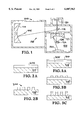
- FIG. 1 is a schematic of an extreme ultraviolet light imaging system according to one preferred embodiment of the present invention.
- FIG. 2 is a process flow for developing a demagnified image in a resist according to one embodiment of the present invention.
- FIG. 3 is a process flow for developing a demagnified image in a bi-layer resist according to a second embodiment of the present invention.
- FIG. 4 shows a dark field optical micrograph of a patterning obtained using the extreme ultraviolet light system according to the preferred embodiment of the present invention.
- FIG. 5 is a second micrograph showing three gates of the printed field displayed in FIG. 4.
- FIG. 6 is an electron micrograph at four times higher magnification, i.e. 60,000 ⁇ , of the same structure of FIG. 5.
- EUVL extreme ultraviolet light lithography
- the EUVL system 100 comprises a laser produced plasma source 105, a condenser 110 and a turning mirror 115 which together form an illumination system 135, a translating reflective object mask 120, a Schwarzschild camera 125, a photoresist coated wafer 130 and the associated vacuum apparatus (not shown).
- a plasma is produced when a target, 105, irradiated by a high energy laser such as an excimer laser and preferably a pulsed Nd:YAG laser operating at 1.06 nm and having greater than 120 watts of power, is vaporized.
- the target 105 can be a liquid or a solid metal, preferably gold, however, other materials such as copper, tantalum, tungsten, and tin can also be used.
- Tungsten targets have been found to be somewhat brighter near 13.4 nm than copper targets and tend to emit less debris than either copper and gold, but tungsten targets are difficult to operate reliably over the extended periods due to brittle fracture and flaking characteristics.
- Pellets comprised of frozen gas, such as Xe, or a Van der Waals gas cluster comprising such UV radiators as H 2 O, CF 4 , HCl, O 2 , Ar, Kr and Xe also make desirable target materials
- the EUV radiation is generated by a laser plasma, electric discharge or a synchrotron radiation storage ring can also be utilized.
- the EUV rays, generated by target 105 are collected by the condenser 110 and reflected down the length of a vacuum structure (not shown) to the turning mirror 115.
- the turning mirror 115 is aligned to reflect the EUV rays and provide a 5 mm Kohler-illuminated spot on the reflective mask 120 for reflection into the Schwarzschild camera 125 as described below.
- the reflective mask 120 comprises absorptive regions and reflective regions whereby a patterned image is reflected to Schwarzchild camera 125.
- the reflective mask 120 can be a molybdenum and silicon multi-layer coated fused silica flat patterned with a bi-layer absorber having 60 nm of hard baked resist and 30 nm of germanium.
- All of the reflective mirror surfaces needed to reflect the extreme ultraviolet rays are coated with precisely-matched multilayer Bragg reflective coatings comprising periodic alternating layers of molybdenum and silicon or molybdenum and beryllium having bilayer periods equal to approximately half of the reflected wavelength at normal incidence.
- these multilayer mirrors can be deposited on the imaging system elements with graded multilayer periods to maintain the wavelength of peak reflectance as the angle of incidence changes across the figure of each element of the imaging system.
- photoresist 200 which is at least partially transparent to EUV.
- Photoresist materials such as organosilicon polymers, boron carbide polymers, pure hydrocarbon polymers (containing little or no oxygen, which is strongly attenuating for short wavelength radiation) and/or hydrochlorocarbons, can be used individually or in combination.
- the photoresist layer 205 is deposited by spinning or evaporation over a silicon or other flat substrate 210.
- the photoresist can contain 50-80 atomic percent carbon and 15-30 atomic percent chlorine and 20-50 atomic percent boron or other elements, such as beryllium, making it more transparent to EUV radiation than traditional organic photoresists.
- the photoresist comprises an organosilicon polymer, poly(cyclohexylmethyl-co-trimethylsilylmethyl silane), in which the weight percentage of silicon is 35%.
- the photoresist layer thickness can be made thin enough to yield adequate film penetration by the EUV radiation.
- a thickness of 110 nm of the etch-resistant co-polymer of chloromethacrylate and methylstyrene such as ZEP 520 (commercially available from Nippon Zeon) is adequate. The etch resistance of this thinner layer must then be large enough to compensate for its reduced thickness.
- the photoresist 205 is exposed to the extreme ultraviolet image of the mask pattern as projected by the imaging system mirrors located in the Schwarzchild camera.
- the pattern formed in the resist by this projected image can be revealed by developing the photoresist layer with a solvent or solution which dissolves away the exposed photoresist giving rise to the patterned structure 220.
- the remaining photoresist can be used as an etch barrier in the normal way to fabricate structures, such as gate apertures for field emitter arrays (FEA).
- a positive tone process is utilized.
- a negative tone process can be employed through the use of resists that cross-link or densify upon EUV exposure.
- a second photoresist configuration is shown which is also useful for producing a patterned array of submicron apertures and other structures by means of EUV lithography.
- a bi-layer photoresist compatible with the teachings of the present invention is shown.
- the bi-layer is formed by first depositing a 0.5-1 ⁇ m thick planarizing layer 305 which is then covered with a thin etch-resistant imaging layer 310 on the surface of a silicon or other wafer 315 to be processed.
- the planarizing layer 305 can be an organic polymer, such as hard-baked novolac having a thickness of about 0.5 ⁇ m, or a plasma-deposited carbon film.
- the imaging layer 310 is a 0.1-0.2 ⁇ m thick layer formed from polymers such as polysilanes, polysiloxanes, or polygermanes (polysilanes being preferred because of their total lack of oxygen) and includes elements that impart etch resistance to the imaging layer.
- polymers such as polysilanes, polysiloxanes, or polygermanes (polysilanes being preferred because of their total lack of oxygen) and includes elements that impart etch resistance to the imaging layer.
- silicon is present as a repeating polysilane (--Si--Si--Si) n or as a polysiloxane (--Si--O--Si--O) n .
- boron carbides vanadium oxides (V 2 O 5 ), molybdenum oxides (MoO 3 ), or organotitanates, such as [Ti--(OCxHy) 2 ] may also be used as pure films of each or in combination.
- the planarizing layer is "hard-baked" at a temperature of 160-200C. for 30-60 minutes.
- a polysilane such as poly(cyclohexylmethyl-co-trimethylsilylmethyl silane) is dissolved in xylenes to a viscosity appropriate to allow a 150-250 nm thick film to be spin-cast at a rate between 2000-4000 rpm on top of the planarizing layer 305 to form the imaging layer 310.
- the resulting imaging layer 310 is then baked at 125C. for several minutes to drive off all solvents and to allow the layer to flow conformally.
- the photoresist is then exposed to the EUV radiation image which forms the latent image in imaging layer 310.
- the exposed imaging layer 310 is developed using tetrahydrofuran for 1-2 minutes, which dissolves away the exposed regions but not the unexposed regions.
- the resulting patterned imaging layer 310 is now used as an in-situ etch mask to etch through the organic planarizing layer 305 using an oxygen plasma etch preferably at a plasma power of ⁇ 2000 W at an oxygen pressure of ⁇ 2 ⁇ 10 -3 Torr.
- the resulting pattern, shown in FIG. 3c would have a total film thickness of 650-750 nm, yielding a much more robust photoresist layer for subsequent wet or dry etch fabrication of structures such as gate apertures for a FEA.
- FIGS. 3a, b, and c illustrate a negative tone process which can be obtained with a polysiloxane imaging layer.
- a positive tone process is also possible wherein a polysilane, polygermane, vanadium oxide, or molybdenum oxide is used as the imaging layer.
- a patterned array of gates, useful for field emitter arrays was produced using EUV lithography.
- a 120 watt KrF excimer laser was used to produce 0.6 Joule pulses having 25 ns duration at a maximum repetition rate of 200 Hz, and was focused to achieve an intensity of 1-2 ⁇ 10 11 Watts per cm 2 on a gold target.
- the extreme ultraviolet radiation produced from the gold plasma which fell within a 0.155 steradian solid angle (2.5% of the available 2 ⁇ steradians), was collected by a condenser to provide a 5 mm Kohler-illuminated spot on a mask containing nine identical square arrays, each of which contained a 10 by 10 array of circular gates.
- the condenser was positioned so that one focal point was located on the laser plasma source which was located 112.5 mm from the ellipsoidal surface in an extension tube on one side of the camera chamber. The resulting image of the source at focal point was magnified by 13.3 times.
- the Schwarzchild camera was optimized to achieve 0.1 micrometer resolution over a 0.4 mm diameter field of view.
- the Schwarzschild camera included a primary 126 and secondary mirror 127 having modest clear apertures of 14.8 mm and 82 mm, respectively.
- a decentered unobscured numerical aperture of 0.08 was selected by rotating an aperture plate 128 immediately in front of the primary mirror 126, which resulted in a design depth of focus of ⁇ 1.0 ⁇ m.
- the distance between the object and the image planes was 315 mm.
- the calculated modulation for 0.1 micrometer lines and spaces was approximately 0.824 for an unaberrated system illuminated with a pupil fill factor of 0.5.
- Alignment of the primary 126 and secondary mirrors 127 was performed to tolerances of ⁇ 9 ⁇ m in separation and ⁇ 2.5 ⁇ m in decentration.
- the mirror pair used for the present embodiment exhibited a wave front error of 2 nm rms within the relevant subaperture after final alignment. The wave front error exhibited only very slow variation across the subaperture and camera alignment remained stable over a period of several months.
- the source image was reflected by the reflective surfaces of the reflective mask into the 4 mm entrance pupil of the Schwarzschild camera 125, achieving a coherence factor of approximately 0.5. Thereafter, a demagnified image was achieved by reflecting the image pattern from the primary mirror 126 to the secondary mirror 127 which was thereafter reflected onto a target wafer 130.
- a special "sandwich" structure silicon target wafer 130 was prepared which comprised a 0.2 ⁇ m thick molybdenum layer covering a 0.6 ⁇ m thick silicon oxide layer on top of the silicon substrate.
- the molybdenum layer, which was the uppermost layer in the "sandwich” structure was spin-coated with a 110 nm thick layer of ZEP resist.
- the resist was then pre-baked at 200° C. for 2 minutes, cooled and then exposed to the gate array EUV image using the Schwarzschild camera 125. After exposure the resist was developed in xylenes for 5 minutes and rinsed in a mixture of isopropanol and methyl isobutyl ketone.
- FIG. 4 a dark field optical micrograph of the patterning of gate apertures for field emitter arrays is shown having been obtained using the extreme ultraviolet lithography system and employing ZEP photoresist according to the above-described process.
- the print field measures 280 ⁇ m by 280 ⁇ m and was obtained in a single exposure with the Schwarzschild objective illuminated by a laser plasma source, as described earlier.
- the print field shown in FIG. 4 is a pattern of nine identical square arrays, each of which contains a 10 ⁇ 10 array of circular gate apertures, for a total of 900 gate apertures.
- the gate apertures are approximately 0.4 ⁇ m in diameter and spaced on 4 ⁇ m centers.
- FIG. 5 a scanning electron micrograph containing three gates of the printed field of 900 gates is shown.
- FIG. 5 is rotated 45° with respect to FIG. 4.
- FIG. 6 is an electron micrograph at four times higher magnification, i.e. 60,000 ⁇ , of the same structure of FIG. 5.
- the teachings of the present invention allow for sharp well-defined edges in the printed features which may be utilized not only in the fabrication of gates for field emitter arrays but also in other various microelectronic, microoptical and micromechanical fabrication processes.
Abstract
A method of producing a patterned array of features, in particular, gate apertures, in the size range 0.4-0.05 μm using projection lithography and extreme ultraviolet (EUV) radiation. A high energy laser beam is used to vaporize a target material in order to produce a plasma which in turn, produces extreme ultraviolet radiation of a characteristic wavelength of about 13 nm for lithographic applications. The radiation is transmitted by a series of reflective mirrors to a mask which bears the pattern to be printed. The demagnified focused mask pattern is, in turn, transmitted by means of appropriate optics and in a single exposure, to a substrate coated with photoresists designed to be transparent to EUV radiation and also satisfy conventional processing methods.
Description
This invention was made with Government support under contract no. DE-AC04-94AL8500 awarded by the U. S. Department of Energy to Sandia Corporation. The Government has certain rights in the invention.
The following application is a continuation of U.S. patent application Ser. No. 08/532,958 filed Sep. 21, 1995, now abandoned.
This invention pertains generally to microelectronic processing and more particularly to the use of projection lithography employing extreme ultraviolet light for patterning features.
At the present time semiconductor electronics are produced by projection lithographic methods whereby a circuit pattern or blueprint is transferred from a mask onto a silicon wafer. The process is similar to exposing a film negative onto photographic paper except that the transferred image is reduced rather than enlarged thereby making the electronic component smaller. The demand for smaller critical dimensions in advanced computer chips is continuing to spur improvements in projection lithography. Presently, deep ultraviolet lithography systems, operating at 248 nm and producing 0.25 μm features, are now commercially available and 193 nm lithography systems, capable of producing features in the 0.18 μm range, are under development. In order to produce smaller features it is necessary to operate at even shorter wavelengths. By utilizing extreme ultraviolet (EUV) radiation in the range of 4.5-15 nm it is possible to produce features smaller than 0.18 μm. The resolution and therefore, the minimum feature size that can be obtained with EUV is a factor of 2-6 times better than with the present deep-UV or 193 nm lithography. However, as will be discussed below, other features of the projection lithography process have impeded the use of shorter wavelengths.
Photoresists are photosensitive films used in projection lithography for transfer of images to a substrate. They form negative or positive images. After coating a substrate with a photoresist the coated substrate is exposed to a source of activating radiation. This radiation exposure causes a chemical transformation in the exposed areas of the coated surface. After the radiation exposure step, the photoresist-coated substrate is treated with a developer solution to dissolve or otherwise remove either the radiation-exposed or unexposed areas of the coated substrate, depending upon the type of photoresist used. Unfortunately, most photoresist materials absorb extreme ultraviolet (EUV) radiation strongly in the range of 4.5-15 nm. While this is advantageous from the standpoint of resist speed (i.e. the exposure dose required to form a pattern) and the associated printing rate, it poses a serious problem for projection lithographic methods that employ EUV radiation because of highly nonuniform absorption of this radiation through the photoresist thickness. In present photoresist materials, EUV radiation will not penetrate much beyond a film thickness of 0.15 or 0.20 μm. Yet, to fabricate holes and other structures in semiconductor materials such as silicon, as well as metals, or dielectrics, the photoresist layer must be thick enough, preferably 0.5-1.0 μm, to withstand etching and other processing steps. Accordingly, in order to make use of the increased resolution afforded by the use of EUV radiation in the processing and fabrication of small structures, photoresist schemes need to be employed that can be used in conjunction with high resolution EUV radiation and yet are compatible with conventional lithographic processing methods.
As set forth above, the ability to produce smaller dimensions in electronic devices offers significant advantages. Of particular interest is the ability to fabricate gates useful for field emitter applications. The basic technology, projection lithography, useful for fabricating field-imaging and electron-emitting structures has been described by Spindt in U.S. Pat. Nos. 3,812,559; 3,665,241; 3,755,704; 3,789,471 and 5,064,396. Smaller gates allow these devices to operate efficiently at significantly lower voltages. By operating at lower voltages inexpensive drive electronics can be used. With a gate size of 0.4 μm, it is possible to employ CMOS circuitry rather than the more expensive bipolar circuits required for 1 μm gates fabricated conventionally. Lower voltages also permit lower power operation and, therefore greater efficiency. Smaller gates permit higher tip packing density and a corresponding reduction in the current required from an average tip, thereby improving the lifetime of the tips. These desirable smaller features cannot be produced by present semiconductor fabrication technology. Consequently, having the ability to fabricate a patterned array of gates with an aperture size of 0.4 μm or smaller is desirable. These same advantages pertain to semiconductor and other electronic devices.
The invention described herein employs EUV radiation in the range of about 4.5 to 15 nm for performing projection lithography in order to produce patterns and features, in particular, apertures, in the size range of about 0.4-0.05 μm. The present invention overcomes difficulties encountered in using conventional photoresists with short wavelength radiation by providing photoresists designed to accommodate EUV radiation and at the same time satisfy conventional lithographic processing requirements. This invention further improves over existing short wavelength projection lithography technology by the use of an imaging camera which permits all of the desired structures or features (holes, tubes, channels, pedestals, etc.) to be printed during a single exposure allowing for greatly increased patterning rates compared with techniques such as electron beam and ion beam lithography methods in which printing of repetitive features requires time consuming multiple exposures.
In EUV lithography (EUVL) a high energy laser beam is used to vaporize a target material to produce a plasma which in turn, produces radiation of a characteristic wavelength. The composition of the target material generally determines the wavelength of the radiation produced. For 13 nm radiation, gold is the preferred target material although other target materials such as copper, tantalum, tungsten and tin may be used. Alternatively, a synchrotron radiation source could be employed as the EUV source. The radiation is transmitted by a series of reflective mirrors to a mask.
In conventional lithography, masks are comprised of optically dense regions in which light is absorbed and less dense regions through which light is transmitted, thereby defining the pattern to be printed. However, EUV radiation is strongly absorbed by most mask materials therefore, in EUVL a reflective mask is necessary. The mask comprises a highly reflective periodic multi-layer substrate and a non-reflective absorber pattern that bears the pattern to be printed. The radiation reflected from this pattern mask enters an all-reflective camera which forms a focused image of the mask demagnified (reduced) by a factor of typically between 4 and 10, and allows for image formation over a large exposure field. The imaging camera employed in EUVL is a Schwarzschild camera such as that described in U.S. Pat. No. 5,291,339, incorporated herein by reference, although other methods of forming demagnified images, known to those skilled in the art, may be used.
The mask pattern is, in turn, transmitted by means of appropriate optics to the substrate where it is to be printed. The substrate is coated with either a positive-working or negative-working resist comprising materials which are transparent to the EUV radiation. The soluble portion of the photoresist is then removed by an appropriate solvent. A system capable of projecting a magnified or demagnified image of an existing pattern from a mask onto a photoresist coated substrate is described in U.S. Pat. No. 5,003,567, incorporated herein by reference.
In the present invention two resist schemes are employed in order to accommodate short wavelength EUV radiation and also to satisfy normal processing step requirements. In the first embodiment, a single layer resist scheme is employed in which resists whose composition makes them more transparent to 13 nm radiation than traditional resists are utilized. In the second and preferred embodiment, a bi-layer resist scheme provides for a planarizing layer covered with a thin etch resistant imaging layer. For EUVL applications bi-layer resists offer increased resolution and sensitivity over the more traditional single layer resists, even those especially tailored to be transparent to 13 nm radiation. This is because in single layer resists resolution and linewidth control become difficult due to standing wave effects in the film over topography of a different refractive index. In bi-layer resists, imaging takes place only in the thin radiation sensitive imaging layer and this pattern is then transferred, by means of a plasma etching step, to an underlying planarizing layer.
Accordingly, it is an object of this invention to provide a method for fabricating submicron features on a substrate. It is a further object of this invention to provide a method for fabricating a patterned array of submicron apertures and other structures on semiconducting materials such as silicon, as well as metals and dielectrics. It is another object to provide a method for fabricating submicron features on a substrate wherein the printing rate is increased by employing a patterned array and a single exposure. Yet another object is to provide an improved photosensitive material such as a resist with an enhanced transparency to 13 nm radiation.
The accompanying drawings, which are incorporated in and form a part of this specification, illustrate embodiments of the invention and, together with the detailed description, serve to explain the principles of the invention in which:
FIG. 1 is a schematic of an extreme ultraviolet light imaging system according to one preferred embodiment of the present invention.
FIG. 2 is a process flow for developing a demagnified image in a resist according to one embodiment of the present invention.
FIG. 3 is a process flow for developing a demagnified image in a bi-layer resist according to a second embodiment of the present invention.
FIG. 4 shows a dark field optical micrograph of a patterning obtained using the extreme ultraviolet light system according to the preferred embodiment of the present invention.
FIG. 5 is a second micrograph showing three gates of the printed field displayed in FIG. 4.
FIG. 6 is an electron micrograph at four times higher magnification, i.e. 60,000×, of the same structure of FIG. 5.
The present invention now will be described more fully hereinafter with reference to the accompanying drawings in which the preferred embodiments of the invention are shown. This invention may, however, be embodied in many different forms and should not be construed as limited to the embodiment set forth herein.
Referring now to FIG. 1, an extreme ultraviolet light lithography (EUVL) system 100 for patterning features according to the present invention is shown. The EUVL system 100 comprises a laser produced plasma source 105, a condenser 110 and a turning mirror 115 which together form an illumination system 135, a translating reflective object mask 120, a Schwarzschild camera 125, a photoresist coated wafer 130 and the associated vacuum apparatus (not shown).
A plasma is produced when a target, 105, irradiated by a high energy laser such as an excimer laser and preferably a pulsed Nd:YAG laser operating at 1.06 nm and having greater than 120 watts of power, is vaporized. The target 105 can be a liquid or a solid metal, preferably gold, however, other materials such as copper, tantalum, tungsten, and tin can also be used. Tungsten targets have been found to be somewhat brighter near 13.4 nm than copper targets and tend to emit less debris than either copper and gold, but tungsten targets are difficult to operate reliably over the extended periods due to brittle fracture and flaking characteristics. Pellets comprised of frozen gas, such as Xe, or a Van der Waals gas cluster comprising such UV radiators as H2 O, CF4, HCl, O2, Ar, Kr and Xe also make desirable target materials
Those skilled in the art will recognize that other radiation sources may be utilized to produce the extreme ultraviolet light having a wavelength between 4 nm and 15 nm. Accordingly, while in the preferred embodiment the EUV radiation is generated by a laser plasma, electric discharge or a synchrotron radiation storage ring can also be utilized.
In operation, the EUV rays, generated by target 105, are collected by the condenser 110 and reflected down the length of a vacuum structure (not shown) to the turning mirror 115. The turning mirror 115 is aligned to reflect the EUV rays and provide a 5 mm Kohler-illuminated spot on the reflective mask 120 for reflection into the Schwarzschild camera 125 as described below.
The reflective mask 120 comprises absorptive regions and reflective regions whereby a patterned image is reflected to Schwarzchild camera 125. In one preferred embodiment, the reflective mask 120 can be a molybdenum and silicon multi-layer coated fused silica flat patterned with a bi-layer absorber having 60 nm of hard baked resist and 30 nm of germanium.
All of the reflective mirror surfaces needed to reflect the extreme ultraviolet rays are coated with precisely-matched multilayer Bragg reflective coatings comprising periodic alternating layers of molybdenum and silicon or molybdenum and beryllium having bilayer periods equal to approximately half of the reflected wavelength at normal incidence. Moreover, these multilayer mirrors can be deposited on the imaging system elements with graded multilayer periods to maintain the wavelength of peak reflectance as the angle of incidence changes across the figure of each element of the imaging system.
Referring now to FIG. 2, a single layer photoresist 200, which is at least partially transparent to EUV, is shown. Photoresist materials such as organosilicon polymers, boron carbide polymers, pure hydrocarbon polymers (containing little or no oxygen, which is strongly attenuating for short wavelength radiation) and/or hydrochlorocarbons, can be used individually or in combination. In this embodiment, the photoresist layer 205 is deposited by spinning or evaporation over a silicon or other flat substrate 210. For the purposes of this invention, the photoresist can contain 50-80 atomic percent carbon and 15-30 atomic percent chlorine and 20-50 atomic percent boron or other elements, such as beryllium, making it more transparent to EUV radiation than traditional organic photoresists. Increasing the atomic percentage of silicon in the photoresist improves its performance. In one embodiment the photoresist comprises an organosilicon polymer, poly(cyclohexylmethyl-co-trimethylsilylmethyl silane), in which the weight percentage of silicon is 35%. Alternatively, or in combination with such embodiment, the photoresist layer thickness can be made thin enough to yield adequate film penetration by the EUV radiation. Typically, a thickness of 110 nm of the etch-resistant co-polymer of chloromethacrylate and methylstyrene such as ZEP 520 (commercially available from Nippon Zeon) is adequate. The etch resistance of this thinner layer must then be large enough to compensate for its reduced thickness. In operation, the photoresist 205 is exposed to the extreme ultraviolet image of the mask pattern as projected by the imaging system mirrors located in the Schwarzchild camera. The pattern formed in the resist by this projected image can be revealed by developing the photoresist layer with a solvent or solution which dissolves away the exposed photoresist giving rise to the patterned structure 220. The remaining photoresist can be used as an etch barrier in the normal way to fabricate structures, such as gate apertures for field emitter arrays (FEA). In one preferred embodiment, a positive tone process is utilized. Alternatively, a negative tone process can be employed through the use of resists that cross-link or densify upon EUV exposure.
Referring now to FIG. 3, a second photoresist configuration is shown which is also useful for producing a patterned array of submicron apertures and other structures by means of EUV lithography. Here a bi-layer photoresist compatible with the teachings of the present invention is shown. The bi-layer is formed by first depositing a 0.5-1 μm thick planarizing layer 305 which is then covered with a thin etch-resistant imaging layer 310 on the surface of a silicon or other wafer 315 to be processed. The planarizing layer 305 can be an organic polymer, such as hard-baked novolac having a thickness of about 0.5 μm, or a plasma-deposited carbon film. The imaging layer 310 is a 0.1-0.2 μm thick layer formed from polymers such as polysilanes, polysiloxanes, or polygermanes (polysilanes being preferred because of their total lack of oxygen) and includes elements that impart etch resistance to the imaging layer. Preferably silicon is present as a repeating polysilane (--Si--Si--Si)n or as a polysiloxane (--Si--O--Si--O)n. Alternatively, boron carbides, vanadium oxides (V2 O5), molybdenum oxides (MoO3), or organotitanates, such as [Ti--(OCxHy)2 ] may also be used as pure films of each or in combination.
The planarizing layer is "hard-baked" at a temperature of 160-200C. for 30-60 minutes. A polysilane, such as poly(cyclohexylmethyl-co-trimethylsilylmethyl silane) is dissolved in xylenes to a viscosity appropriate to allow a 150-250 nm thick film to be spin-cast at a rate between 2000-4000 rpm on top of the planarizing layer 305 to form the imaging layer 310. The resulting imaging layer 310 is then baked at 125C. for several minutes to drive off all solvents and to allow the layer to flow conformally.
The photoresist is then exposed to the EUV radiation image which forms the latent image in imaging layer 310. The exposed imaging layer 310 is developed using tetrahydrofuran for 1-2 minutes, which dissolves away the exposed regions but not the unexposed regions. The resulting patterned imaging layer 310 is now used as an in-situ etch mask to etch through the organic planarizing layer 305 using an oxygen plasma etch preferably at a plasma power of ˜2000 W at an oxygen pressure of ˜2×10⁻³ Torr. The resulting pattern, shown in FIG. 3c would have a total film thickness of 650-750 nm, yielding a much more robust photoresist layer for subsequent wet or dry etch fabrication of structures such as gate apertures for a FEA. An example of such a process for vanadium oxide, the V2 O5 layer would be vapor deposited to a thickness of only 10-20 nm on top of the planarizing layer. The latent image is developed in nitric acid to reveal the patterned image. The pattern is then transferred to the planarizing layer 305 with a reactive ion etch. FIGS. 3a, b, and c illustrate a negative tone process which can be obtained with a polysiloxane imaging layer. A positive tone process is also possible wherein a polysilane, polygermane, vanadium oxide, or molybdenum oxide is used as the imaging layer.
As an example of the process disclosed herein, a patterned array of gates, useful for field emitter arrays, was produced using EUV lithography.
A 120 watt KrF excimer laser was used to produce 0.6 Joule pulses having 25 ns duration at a maximum repetition rate of 200 Hz, and was focused to achieve an intensity of 1-2×10¹¹ Watts per cm2 on a gold target. The extreme ultraviolet radiation produced from the gold plasma, which fell within a 0.155 steradian solid angle (2.5% of the available 2πsteradians), was collected by a condenser to provide a 5 mm Kohler-illuminated spot on a mask containing nine identical square arrays, each of which contained a 10 by 10 array of circular gates. The condenser was positioned so that one focal point was located on the laser plasma source which was located 112.5 mm from the ellipsoidal surface in an extension tube on one side of the camera chamber. The resulting image of the source at focal point was magnified by 13.3 times. The Schwarzchild camera was optimized to achieve 0.1 micrometer resolution over a 0.4 mm diameter field of view. The Schwarzschild camera included a primary 126 and secondary mirror 127 having modest clear apertures of 14.8 mm and 82 mm, respectively. A decentered unobscured numerical aperture of 0.08 was selected by rotating an aperture plate 128 immediately in front of the primary mirror 126, which resulted in a design depth of focus of ±1.0 μm. The distance between the object and the image planes was 315 mm. The calculated modulation for 0.1 micrometer lines and spaces was approximately 0.824 for an unaberrated system illuminated with a pupil fill factor of 0.5. Alignment of the primary 126 and secondary mirrors 127 was performed to tolerances of ±9 μm in separation and ±2.5 μm in decentration. The mirror pair used for the present embodiment exhibited a wave front error of 2 nm rms within the relevant subaperture after final alignment. The wave front error exhibited only very slow variation across the subaperture and camera alignment remained stable over a period of several months.
In operation, the source image was reflected by the reflective surfaces of the reflective mask into the 4 mm entrance pupil of the Schwarzschild camera 125, achieving a coherence factor of approximately 0.5. Thereafter, a demagnified image was achieved by reflecting the image pattern from the primary mirror 126 to the secondary mirror 127 which was thereafter reflected onto a target wafer 130.
A special "sandwich" structure silicon target wafer 130 was prepared which comprised a 0.2 μm thick molybdenum layer covering a 0.6 μm thick silicon oxide layer on top of the silicon substrate. The molybdenum layer, which was the uppermost layer in the "sandwich" structure was spin-coated with a 110 nm thick layer of ZEP resist. The resist was then pre-baked at 200° C. for 2 minutes, cooled and then exposed to the gate array EUV image using the Schwarzschild camera 125. After exposure the resist was developed in xylenes for 5 minutes and rinsed in a mixture of isopropanol and methyl isobutyl ketone.
Referring now to FIG. 4, a dark field optical micrograph of the patterning of gate apertures for field emitter arrays is shown having been obtained using the extreme ultraviolet lithography system and employing ZEP photoresist according to the above-described process. The print field measures 280 μm by 280 μm and was obtained in a single exposure with the Schwarzschild objective illuminated by a laser plasma source, as described earlier. The print field shown in FIG. 4 is a pattern of nine identical square arrays, each of which contains a 10×10 array of circular gate apertures, for a total of 900 gate apertures. The gate apertures are approximately 0.4 μm in diameter and spaced on 4 μm centers.
Referring now to FIG. 5, a scanning electron micrograph containing three gates of the printed field of 900 gates is shown. FIG. 5 is rotated 45° with respect to FIG. 4. FIG. 6 is an electron micrograph at four times higher magnification, i.e. 60,000×, of the same structure of FIG. 5. As shown in FIG. 6, the teachings of the present invention allow for sharp well-defined edges in the printed features which may be utilized not only in the fabrication of gates for field emitter arrays but also in other various microelectronic, microoptical and micromechanical fabrication processes.
The foregoing descriptions are illustrative of the invention and should not be construed as limiting. Various modifications may occur to those skilled in the art without departing from the scope of the invention as defined by the appended claims.
Claims (1)
1. A bi-layer photoresist for replicating a patterned array of features on a surface of a substrate material comprising:
a planarizing layer applied to and covering said substrate surface, wherein said planarizing layer is novolac or plasma-deposited carbon said planarizing layer at least about 0.5 μm thick; and
an imaging layer applied to and covering said planarizing layer, wherein said imaging layer is selected from the group consisting essentially of poly(cyclohexylmethyl-co-trimethylsilylmethyl silane), boron carbide, vanadium oxide, molybdenum oxide, said imaging layer at least partially transparent to radiation having a wavelength between about 15 nm to about 4.5 nm, said imaging layer between about 0.1 μm to about 0.2 μm thick.
Priority Applications (3)
| Application Number | Priority Date | Filing Date | Title |
|---|---|---|---|
| US08/877,031 US6007963A (en) | 1995-09-21 | 1997-06-17 | Method for extreme ultraviolet lithography |
| US09/158,943 US6162577A (en) | 1995-09-21 | 1998-09-21 | Method for extreme ultraviolet lithography |
| US09/158,948 US5989776A (en) | 1995-09-21 | 1998-09-21 | Photoresist composition for extreme ultraviolet lithography |
Applications Claiming Priority (2)
| Application Number | Priority Date | Filing Date | Title |
|---|---|---|---|
| US53295895A | 1995-09-21 | 1995-09-21 | |
| US08/877,031 US6007963A (en) | 1995-09-21 | 1997-06-17 | Method for extreme ultraviolet lithography |
Related Parent Applications (1)
| Application Number | Title | Priority Date | Filing Date |
|---|---|---|---|
| US53295895A Continuation | 1995-09-21 | 1995-09-21 |
Related Child Applications (2)
| Application Number | Title | Priority Date | Filing Date |
|---|---|---|---|
| US09/158,943 Division US6162577A (en) | 1995-09-21 | 1998-09-21 | Method for extreme ultraviolet lithography |
| US09/158,948 Division US5989776A (en) | 1995-09-21 | 1998-09-21 | Photoresist composition for extreme ultraviolet lithography |
Publications (1)
| Publication Number | Publication Date |
|---|---|
| US6007963A true US6007963A (en) | 1999-12-28 |
Family
ID=24123906
Family Applications (3)
| Application Number | Title | Priority Date | Filing Date |
|---|---|---|---|
| US08/877,031 Expired - Fee Related US6007963A (en) | 1995-09-21 | 1997-06-17 | Method for extreme ultraviolet lithography |
| US09/158,943 Expired - Fee Related US6162577A (en) | 1995-09-21 | 1998-09-21 | Method for extreme ultraviolet lithography |
| US09/158,948 Expired - Fee Related US5989776A (en) | 1995-09-21 | 1998-09-21 | Photoresist composition for extreme ultraviolet lithography |
Family Applications After (2)
| Application Number | Title | Priority Date | Filing Date |
|---|---|---|---|
| US09/158,943 Expired - Fee Related US6162577A (en) | 1995-09-21 | 1998-09-21 | Method for extreme ultraviolet lithography |
| US09/158,948 Expired - Fee Related US5989776A (en) | 1995-09-21 | 1998-09-21 | Photoresist composition for extreme ultraviolet lithography |
Country Status (1)
| Country | Link |
|---|---|
| US (3) | US6007963A (en) |
Cited By (21)
| Publication number | Priority date | Publication date | Assignee | Title |
|---|---|---|---|---|
| US6324256B1 (en) | 2000-08-23 | 2001-11-27 | Trw Inc. | Liquid sprays as the target for a laser-plasma extreme ultraviolet light source |
| US6433917B1 (en) | 2000-11-22 | 2002-08-13 | Ball Semiconductor, Inc. | Light modulation device and system |
| US6473220B1 (en) | 1998-01-22 | 2002-10-29 | Trivium Technologies, Inc. | Film having transmissive and reflective properties |
| US20030025979A1 (en) * | 2001-07-31 | 2003-02-06 | Ball Semiconductor, Inc. | Surface distortion compensated photolithography |
| US6633048B2 (en) | 2001-05-03 | 2003-10-14 | Northrop Grumman Corporation | High output extreme ultraviolet source |
| US20030210717A1 (en) * | 2002-05-08 | 2003-11-13 | Harry Rieger | Method and system for providing a pulse laser |
| US20030215749A1 (en) * | 2002-04-24 | 2003-11-20 | Hirokazu Kato | Pattern forming method and method for manufacturing semiconductor device |
| US6653054B2 (en) * | 2000-07-26 | 2003-11-25 | FRANCE TéLéCOM | Resin, a double resin layer for extreme ultraviolet light (EUV) photolithography, and an extreme ultraviolet light (EUV) photolithography process |
| US6657213B2 (en) | 2001-05-03 | 2003-12-02 | Northrop Grumman Corporation | High temperature EUV source nozzle |
| US6661018B1 (en) | 2000-04-25 | 2003-12-09 | Northrop Grumman Corporation | Shroud nozzle for gas jet control in an extreme ultraviolet light source |
| US20040198892A1 (en) * | 2003-04-01 | 2004-10-07 | Cabot Microelectronics Corporation | Electron source and method for making same |
| EP1480078A1 (en) * | 2003-05-21 | 2004-11-24 | ASML Netherlands B.V. | Method for coating a substrate for EUV lithography and substrate with photoresist layer |
| US20050008864A1 (en) * | 2003-05-21 | 2005-01-13 | Asml Netherlands B.V. | Method for coating a substrate for euv lithography and substrate with photoresist layer |
| US20050093041A1 (en) * | 2002-03-01 | 2005-05-05 | Carl Zeiss Smt Ag | Illumination system having a nested collector for annular illumination of an exit pupil |
| US6963395B2 (en) * | 2001-07-09 | 2005-11-08 | The Regents Of The University Of California | Method and apparatus for inspecting an EUV mask blank |
| US20060049359A1 (en) * | 2003-04-01 | 2006-03-09 | Cabot Microelectronics Corporation | Decontamination and sterilization system using large area x-ray source |
| US20080258085A1 (en) * | 2004-07-28 | 2008-10-23 | Board Of Regents Of The University & Community College System Of Nevada On Behalf Of Unv | Electro-Less Discharge Extreme Ultraviolet Light Source |
| US7573642B2 (en) | 2002-03-26 | 2009-08-11 | Brilliant Film Llc | System for collimating backlight |
| US7573550B2 (en) | 2003-05-20 | 2009-08-11 | Brilliant Film, Llc | Devices for use in non-emissive displays |
| US7595934B2 (en) | 2002-03-26 | 2009-09-29 | Brilliant Film Llc | Integrated sub-assembly having a light collimating or transflecting device |
| US8226253B2 (en) | 2008-02-27 | 2012-07-24 | Lubart Neil D | Concentrators for solar power generating systems |
Families Citing this family (42)
| Publication number | Priority date | Publication date | Assignee | Title |
|---|---|---|---|---|
| US5998759A (en) * | 1996-12-24 | 1999-12-07 | General Scanning, Inc. | Laser processing |
| US6140200A (en) * | 1998-09-02 | 2000-10-31 | Micron Technology, Inc. | Methods of forming void regions dielectric regions and capacitor constructions |
| US6165695A (en) * | 1998-12-01 | 2000-12-26 | Advanced Micro Devices, Inc. | Thin resist with amorphous silicon hard mask for via etch application |
| US6162587A (en) * | 1998-12-01 | 2000-12-19 | Advanced Micro Devices | Thin resist with transition metal hard mask for via etch application |
| US6306560B1 (en) * | 1998-12-02 | 2001-10-23 | Advanced Micro Devices, Inc. | Ultra-thin resist and SiON/oxide hard mask for metal etch |
| US6171763B1 (en) * | 1998-12-02 | 2001-01-09 | Advanced Micro Devices, Inc. | Ultra-thin resist and oxide/nitride hard mask for metal etch |
| US6300590B1 (en) * | 1998-12-16 | 2001-10-09 | General Scanning, Inc. | Laser processing |
| US6573978B1 (en) * | 1999-01-26 | 2003-06-03 | Mcguire, Jr. James P. | EUV condenser with non-imaging optics |
| JP3299215B2 (en) * | 1999-03-12 | 2002-07-08 | 松下電器産業株式会社 | Pattern formation method |
| USRE41220E1 (en) | 1999-07-22 | 2010-04-13 | Corning Incorporated | Extreme ultraviolet soft x-ray projection lithographic method system and lithographic elements |
| EP1218796A4 (en) | 1999-07-22 | 2006-08-23 | Corning Inc | Extreme ultraviolet soft x-ray projection lithographic method and mask devices |
| JP4374735B2 (en) * | 1999-08-11 | 2009-12-02 | 株式会社ニコン | Reflective soft X-ray microscope, mask inspection apparatus, and reflective mask manufacturing method |
| US6776006B2 (en) | 2000-10-13 | 2004-08-17 | Corning Incorporated | Method to avoid striae in EUV lithography mirrors |
| US6589711B1 (en) | 2001-04-04 | 2003-07-08 | Advanced Micro Devices, Inc. | Dual inlaid process using a bilayer resist |
| US6458691B1 (en) | 2001-04-04 | 2002-10-01 | Advanced Micro Devices, Inc. | Dual inlaid process using an imaging layer to protect via from poisoning |
| US6861273B2 (en) * | 2001-04-30 | 2005-03-01 | Euv Llc | Method of fabricating reflection-mode EUV diffusers |
| US6798494B2 (en) * | 2001-08-30 | 2004-09-28 | Euv Llc | Apparatus for generating partially coherent radiation |
| JP3728495B2 (en) * | 2001-10-05 | 2005-12-21 | 独立行政法人産業技術総合研究所 | Multilayer mask defect inspection method and apparatus |
| US6900139B1 (en) * | 2002-04-30 | 2005-05-31 | Advanced Micro Devices, Inc. | Method for photoresist trim endpoint detection |
| JP3647834B2 (en) * | 2002-09-25 | 2005-05-18 | 松下電器産業株式会社 | Mirror for exposure apparatus, reflective mask for exposure apparatus, exposure apparatus and pattern forming method |
| US20040161619A1 (en) * | 2002-12-12 | 2004-08-19 | Arch Specialty Chemicals, Inc. | Process for producing a heat resistant relief structure |
| US6642531B1 (en) * | 2002-12-23 | 2003-11-04 | Intel Corporation | Contamination control on lithography components |
| US7326514B2 (en) * | 2003-03-12 | 2008-02-05 | Cornell Research Foundation, Inc. | Organoelement resists for EUV lithography and methods of making the same |
| US20040265748A1 (en) * | 2003-06-30 | 2004-12-30 | Robert Bristol | Pattern transfer of an extreme ultraviolet imaging layer via flood exposure of contact mask layer (EUV CML) |
| US7276328B1 (en) * | 2004-03-02 | 2007-10-02 | Advanced Micro Devices, Inc. | Lithography mask utilizing asymmetric light source |
| WO2006080909A1 (en) * | 2005-01-24 | 2006-08-03 | Underwood James H | Extreme ultraviolet reflectometer with rotating grating monochrometer |
| JP5042494B2 (en) * | 2005-12-22 | 2012-10-03 | インテル コーポレイション | Detection and characterization of mask blank defects using angular distribution of scattered light. |
| US7817246B2 (en) * | 2006-06-21 | 2010-10-19 | Asml Netherlands B.V. | Optical apparatus |
| US10437150B2 (en) * | 2008-11-27 | 2019-10-08 | Nissan Chemical Industries, Ltd. | Composition for forming resist underlayer film with reduced outgassing |
| JP5561192B2 (en) * | 2010-02-26 | 2014-07-30 | 信越化学工業株式会社 | High molecular compound, chemically amplified positive resist composition using the same, and pattern forming method |
| JP5505371B2 (en) | 2010-06-01 | 2014-05-28 | 信越化学工業株式会社 | Polymer compound, chemically amplified positive resist material, and pattern forming method |
| WO2012050015A1 (en) * | 2010-10-13 | 2012-04-19 | セントラル硝子株式会社 | Polymerizable fluorine-containing sulfonate, fluorine-containing sulfonate resin, resist composition and pattern-forming method using same |
| JP5278406B2 (en) | 2010-11-02 | 2013-09-04 | 信越化学工業株式会社 | Pattern formation method |
| JP5601309B2 (en) | 2010-11-29 | 2014-10-08 | 信越化学工業株式会社 | Positive resist material and pattern forming method using the same |
| JP5601286B2 (en) * | 2011-07-25 | 2014-10-08 | 信越化学工業株式会社 | Resist material and pattern forming method using the same |
| JP5597616B2 (en) * | 2011-10-03 | 2014-10-01 | 富士フイルム株式会社 | Negative chemically amplified resist composition, and resist film, resist-coated mask blank, resist pattern forming method, and photomask using the same |
| KR102306612B1 (en) * | 2014-01-31 | 2021-09-29 | 램 리써치 코포레이션 | Vacuum-integrated hardmask processes and apparatus |
| US9996004B2 (en) | 2015-11-20 | 2018-06-12 | Lam Research Corporation | EUV photopatterning of vapor-deposited metal oxide-containing hardmasks |
| US10796912B2 (en) | 2017-05-16 | 2020-10-06 | Lam Research Corporation | Eliminating yield impact of stochastics in lithography |
| TWI733069B (en) * | 2017-12-31 | 2021-07-11 | 美商羅門哈斯電子材料有限公司 | Monomers, polymers and lithographic compositions comprising same |
| WO2020102085A1 (en) | 2018-11-14 | 2020-05-22 | Lam Research Corporation | Methods for making hard masks useful in next-generation lithography |
| JP7189375B2 (en) | 2020-01-15 | 2022-12-13 | ラム リサーチ コーポレーション | Underlayer for photoresist adhesion and dose reduction |
Citations (23)
| Publication number | Priority date | Publication date | Assignee | Title |
|---|---|---|---|---|
| US3665241A (en) * | 1970-07-13 | 1972-05-23 | Stanford Research Inst | Field ionizer and field emission cathode structures and methods of production |
| US3755704A (en) * | 1970-02-06 | 1973-08-28 | Stanford Research Inst | Field emission cathode structures and devices utilizing such structures |
| US3789471A (en) * | 1970-02-06 | 1974-02-05 | Stanford Research Inst | Field emission cathode structures, devices utilizing such structures, and methods of producing such structures |
| US3812559A (en) * | 1970-07-13 | 1974-05-28 | Stanford Research Inst | Methods of producing field ionizer and field emission cathode structures |
| US3873341A (en) * | 1972-12-26 | 1975-03-25 | Material Sciences Corp | Rapid conversion of an iron oxide film |
| US4515886A (en) * | 1983-02-16 | 1985-05-07 | Toyo Soda Manufacturing Co., Ltd. | Photosensitive compositions |
| USH66H (en) * | 1983-12-21 | 1986-05-06 | At&T Bell Laboratories | Pulsed plasma generation of extreme ultraviolet radiation |
| US4588801A (en) * | 1984-04-05 | 1986-05-13 | The United States Of America As Represented By The United States Department Of Energy | Polysilane positive photoresist materials and methods for their use |
| US4619894A (en) * | 1985-04-12 | 1986-10-28 | Massachusetts Institute Of Technology | Solid-transformation thermal resist |
| US4741989A (en) * | 1983-04-01 | 1988-05-03 | Sumitomo Chemical Company, Limited | Positive photoresist aqueous developer solution containing quaternary ammonium hydroxide with aliphatic ketone or cyclic ether alone or with amine as development modifier |
| US4822716A (en) * | 1985-12-27 | 1989-04-18 | Kabushiki Kaisha Toshiba | Polysilanes, Polysiloxanes and silicone resist materials containing these compounds |
| US5003567A (en) * | 1989-02-09 | 1991-03-26 | Hawryluk Andrew M | Soft x-ray reduction camera for submicron lithography |
| US5039593A (en) * | 1986-10-31 | 1991-08-13 | Zeigler John K | Poly(silyl silane) homo and copolymers |
| US5064396A (en) * | 1990-01-29 | 1991-11-12 | Coloray Display Corporation | Method of manufacturing an electric field producing structure including a field emission cathode |
| US5178989A (en) * | 1989-07-21 | 1993-01-12 | Board Of Regents, The University Of Texas System | Pattern forming and transferring processes |
| US5220590A (en) * | 1992-05-05 | 1993-06-15 | General Signal Corporation | X-ray projection lithography camera |
| US5291339A (en) * | 1990-11-30 | 1994-03-01 | Olympus Optical Co., Ltd. | Schwarzschild optical system |
| US5372908A (en) * | 1991-07-08 | 1994-12-13 | Kabushiki Kaisha Toshiba | Photosensitive composition comprising a polysilane and an acid forming compound |
| US5380621A (en) * | 1992-03-03 | 1995-01-10 | International Business Machines Corporation | Mid and deep-UV antireflection coatings and methods for use thereof |
| JPH07124770A (en) * | 1993-10-29 | 1995-05-16 | Kawasaki Steel Corp | Method and equipment for butt laser beam welding of tube |
| US5426016A (en) * | 1990-03-19 | 1995-06-20 | Mitsubishi Denki Kabushiki Kaisha | Method of forming and removing resist pattern |
| US5499282A (en) * | 1994-05-02 | 1996-03-12 | University Of Central Florida | Efficient narrow spectral width soft-X-ray discharge sources |
| US5849465A (en) * | 1996-11-08 | 1998-12-15 | Symetrix Corporation | Photosensitive titanium carboxydiketonate and titanium carboxyketoester precursor solutions and method of patterning integrated circuits using the same |
Family Cites Families (2)
| Publication number | Priority date | Publication date | Assignee | Title |
|---|---|---|---|---|
| US4515883A (en) * | 1983-04-14 | 1985-05-07 | Ricoh Company, Ltd. | Stilbene derivatives, distyryl derivatives and electrophotographic photoconductor comprising at least one of the derivatives |
| US5482317A (en) * | 1993-06-28 | 1996-01-09 | Sandia Corporation | Structurally efficient inflatable protective device |
-
1997
- 1997-06-17 US US08/877,031 patent/US6007963A/en not_active Expired - Fee Related
-
1998
- 1998-09-21 US US09/158,943 patent/US6162577A/en not_active Expired - Fee Related
- 1998-09-21 US US09/158,948 patent/US5989776A/en not_active Expired - Fee Related
Patent Citations (26)
| Publication number | Priority date | Publication date | Assignee | Title |
|---|---|---|---|---|
| US3755704A (en) * | 1970-02-06 | 1973-08-28 | Stanford Research Inst | Field emission cathode structures and devices utilizing such structures |
| US3789471A (en) * | 1970-02-06 | 1974-02-05 | Stanford Research Inst | Field emission cathode structures, devices utilizing such structures, and methods of producing such structures |
| US3665241A (en) * | 1970-07-13 | 1972-05-23 | Stanford Research Inst | Field ionizer and field emission cathode structures and methods of production |
| US3812559A (en) * | 1970-07-13 | 1974-05-28 | Stanford Research Inst | Methods of producing field ionizer and field emission cathode structures |
| US3873341A (en) * | 1972-12-26 | 1975-03-25 | Material Sciences Corp | Rapid conversion of an iron oxide film |
| US4515886A (en) * | 1983-02-16 | 1985-05-07 | Toyo Soda Manufacturing Co., Ltd. | Photosensitive compositions |
| US4741989A (en) * | 1983-04-01 | 1988-05-03 | Sumitomo Chemical Company, Limited | Positive photoresist aqueous developer solution containing quaternary ammonium hydroxide with aliphatic ketone or cyclic ether alone or with amine as development modifier |
| USH66H (en) * | 1983-12-21 | 1986-05-06 | At&T Bell Laboratories | Pulsed plasma generation of extreme ultraviolet radiation |
| US4588801A (en) * | 1984-04-05 | 1986-05-13 | The United States Of America As Represented By The United States Department Of Energy | Polysilane positive photoresist materials and methods for their use |
| US4619894A (en) * | 1985-04-12 | 1986-10-28 | Massachusetts Institute Of Technology | Solid-transformation thermal resist |
| US4822716A (en) * | 1985-12-27 | 1989-04-18 | Kabushiki Kaisha Toshiba | Polysilanes, Polysiloxanes and silicone resist materials containing these compounds |
| US5039593A (en) * | 1986-10-31 | 1991-08-13 | Zeigler John K | Poly(silyl silane) homo and copolymers |
| US5003567A (en) * | 1989-02-09 | 1991-03-26 | Hawryluk Andrew M | Soft x-ray reduction camera for submicron lithography |
| US5178989A (en) * | 1989-07-21 | 1993-01-12 | Board Of Regents, The University Of Texas System | Pattern forming and transferring processes |
| US5064396A (en) * | 1990-01-29 | 1991-11-12 | Coloray Display Corporation | Method of manufacturing an electric field producing structure including a field emission cathode |
| US5426016A (en) * | 1990-03-19 | 1995-06-20 | Mitsubishi Denki Kabushiki Kaisha | Method of forming and removing resist pattern |
| US5291339A (en) * | 1990-11-30 | 1994-03-01 | Olympus Optical Co., Ltd. | Schwarzschild optical system |
| US5372908A (en) * | 1991-07-08 | 1994-12-13 | Kabushiki Kaisha Toshiba | Photosensitive composition comprising a polysilane and an acid forming compound |
| US5380621A (en) * | 1992-03-03 | 1995-01-10 | International Business Machines Corporation | Mid and deep-UV antireflection coatings and methods for use thereof |
| US5401614A (en) * | 1992-03-03 | 1995-03-28 | International Business Machines Corporation | Mid and deep-UV antireflection coatings and methods for use thereof |
| US5482817A (en) * | 1992-03-03 | 1996-01-09 | International Business Machines Corporation | Mid and deep-uv antireflection coatings and methods for use thereof |
| US5554485A (en) * | 1992-03-03 | 1996-09-10 | International Business Machines Corporation | Mid and deep-UV antireflection coatings and methods for use thereof |
| US5220590A (en) * | 1992-05-05 | 1993-06-15 | General Signal Corporation | X-ray projection lithography camera |
| JPH07124770A (en) * | 1993-10-29 | 1995-05-16 | Kawasaki Steel Corp | Method and equipment for butt laser beam welding of tube |
| US5499282A (en) * | 1994-05-02 | 1996-03-12 | University Of Central Florida | Efficient narrow spectral width soft-X-ray discharge sources |
| US5849465A (en) * | 1996-11-08 | 1998-12-15 | Symetrix Corporation | Photosensitive titanium carboxydiketonate and titanium carboxyketoester precursor solutions and method of patterning integrated circuits using the same |
Non-Patent Citations (6)
| Title |
|---|
| Kubiak, et al., "Soft X-ray Resist Characterization: Studies With a Laser Plasma X-ray Source" Proc. SPIE-Int. Soc. Opt. Eng. (1990) pp. 272-281. |
| Kubiak, et al., Soft X ray Resist Characterization: Studies With a Laser Plasma X ray Source Proc. SPIE Int. Soc. Opt. Eng. (1990) pp. 272 281. * |
| Kubiak, G.D., "XUV Resist Characterization: Studies With a Laser Plasma Source" Proc. SPIE-Int. Soc. Opt. Eng. (1990) pp. 283-291. |
| Kubiak, G.D., XUV Resist Characterization: Studies With a Laser Plasma Source Proc. SPIE Int. Soc. Opt. Eng. (1990) pp. 283 291. * |
| Microelectronic Engineering, 21 (1993) 467 470 Elsevier Peters, D. et al. Fabrication of 0.4 um grid apertures for field emission array cathodes . * |
| Microelectronic Engineering, 21 (1993) 467-470 Elsevier Peters, D. et al. "Fabrication of 0.4 um grid apertures for field-emission array cathodes". |
Cited By (28)
| Publication number | Priority date | Publication date | Assignee | Title |
|---|---|---|---|---|
| US6473220B1 (en) | 1998-01-22 | 2002-10-29 | Trivium Technologies, Inc. | Film having transmissive and reflective properties |
| US7236286B2 (en) | 1998-01-22 | 2007-06-26 | Brilliant Film Llc | Device having reflective and transmissive properties |
| US20060023289A1 (en) * | 1998-01-22 | 2006-02-02 | Clikeman Richard W | Device having reflective and transmissive properties |
| US6661018B1 (en) | 2000-04-25 | 2003-12-09 | Northrop Grumman Corporation | Shroud nozzle for gas jet control in an extreme ultraviolet light source |
| US6653054B2 (en) * | 2000-07-26 | 2003-11-25 | FRANCE TéLéCOM | Resin, a double resin layer for extreme ultraviolet light (EUV) photolithography, and an extreme ultraviolet light (EUV) photolithography process |
| US6324256B1 (en) | 2000-08-23 | 2001-11-27 | Trw Inc. | Liquid sprays as the target for a laser-plasma extreme ultraviolet light source |
| US6433917B1 (en) | 2000-11-22 | 2002-08-13 | Ball Semiconductor, Inc. | Light modulation device and system |
| US6633048B2 (en) | 2001-05-03 | 2003-10-14 | Northrop Grumman Corporation | High output extreme ultraviolet source |
| US6657213B2 (en) | 2001-05-03 | 2003-12-02 | Northrop Grumman Corporation | High temperature EUV source nozzle |
| US6963395B2 (en) * | 2001-07-09 | 2005-11-08 | The Regents Of The University Of California | Method and apparatus for inspecting an EUV mask blank |
| US20030025979A1 (en) * | 2001-07-31 | 2003-02-06 | Ball Semiconductor, Inc. | Surface distortion compensated photolithography |
| US20050093041A1 (en) * | 2002-03-01 | 2005-05-05 | Carl Zeiss Smt Ag | Illumination system having a nested collector for annular illumination of an exit pupil |
| US7312462B2 (en) * | 2002-03-01 | 2007-12-25 | Carl Zeiss Smt Ag | Illumination system having a nested collector for annular illumination of an exit pupil |
| US7595934B2 (en) | 2002-03-26 | 2009-09-29 | Brilliant Film Llc | Integrated sub-assembly having a light collimating or transflecting device |
| US7573642B2 (en) | 2002-03-26 | 2009-08-11 | Brilliant Film Llc | System for collimating backlight |
| US7026099B2 (en) * | 2002-04-24 | 2006-04-11 | Kabushiki Kaisha Toshiba | Pattern forming method and method for manufacturing semiconductor device |
| US20030215749A1 (en) * | 2002-04-24 | 2003-11-20 | Hirokazu Kato | Pattern forming method and method for manufacturing semiconductor device |
| US7006540B2 (en) | 2002-05-08 | 2006-02-28 | Jmar Research, Inc. | Method and system for providing a pulse laser |
| US20030210717A1 (en) * | 2002-05-08 | 2003-11-13 | Harry Rieger | Method and system for providing a pulse laser |
| US20060049359A1 (en) * | 2003-04-01 | 2006-03-09 | Cabot Microelectronics Corporation | Decontamination and sterilization system using large area x-ray source |
| US20040198892A1 (en) * | 2003-04-01 | 2004-10-07 | Cabot Microelectronics Corporation | Electron source and method for making same |
| US7447298B2 (en) | 2003-04-01 | 2008-11-04 | Cabot Microelectronics Corporation | Decontamination and sterilization system using large area x-ray source |
| US7573550B2 (en) | 2003-05-20 | 2009-08-11 | Brilliant Film, Llc | Devices for use in non-emissive displays |
| US20050008864A1 (en) * | 2003-05-21 | 2005-01-13 | Asml Netherlands B.V. | Method for coating a substrate for euv lithography and substrate with photoresist layer |
| EP1480078A1 (en) * | 2003-05-21 | 2004-11-24 | ASML Netherlands B.V. | Method for coating a substrate for EUV lithography and substrate with photoresist layer |
| US20080258085A1 (en) * | 2004-07-28 | 2008-10-23 | Board Of Regents Of The University & Community College System Of Nevada On Behalf Of Unv | Electro-Less Discharge Extreme Ultraviolet Light Source |
| US7605385B2 (en) | 2004-07-28 | 2009-10-20 | Board of Regents of the University and Community College System of Nevada, on behlaf of the University of Nevada | Electro-less discharge extreme ultraviolet light source |
| US8226253B2 (en) | 2008-02-27 | 2012-07-24 | Lubart Neil D | Concentrators for solar power generating systems |
Also Published As
| Publication number | Publication date |
|---|---|
| US5989776A (en) | 1999-11-23 |
| US6162577A (en) | 2000-12-19 |
Similar Documents
| Publication | Publication Date | Title |
|---|---|---|
| US6007963A (en) | Method for extreme ultraviolet lithography | |
| Wallraff et al. | Lithographic imaging techniques for the formation of nanoscopic features | |
| EP0773477B1 (en) | Process for producing a phase shift photomask | |
| EP1412817B1 (en) | Damascene extreme ultraviolet lithography (euvl) photomask and method of making | |
| EP0708367B1 (en) | Pattern delineating apparatus for use in the EUV spectrum | |
| US5510230A (en) | Device fabrication using DUV/EUV pattern delineation | |
| JP4818125B2 (en) | Concentrator with sacrificial reflective surface | |
| US20060292459A1 (en) | EUV reflection mask and method for producing it | |
| US6373553B1 (en) | Photo-lithographic method to print a line-space pattern with a pitch equal to half the pitch of the mask | |
| US9146459B2 (en) | Extreme ultraviolet lithography process and mask | |
| EP0581302B1 (en) | Method for fabricating photomasks having a phase shift layer | |
| TWI278013B (en) | Self-aligned pattern formation using dual wavelengths | |
| US11860530B2 (en) | Mask defect prevention | |
| US20020001760A1 (en) | Low thermal distortion Extreme-UV lithography reticle | |
| JP3647834B2 (en) | Mirror for exposure apparatus, reflective mask for exposure apparatus, exposure apparatus and pattern forming method | |
| KR20150059615A (en) | An extreme ultraviolet lithography process and mask | |
| Marsh | Moore’s law at the extremes | |
| US20220334462A1 (en) | Photomask and method of fabricating a photomask | |
| US6653054B2 (en) | Resin, a double resin layer for extreme ultraviolet light (EUV) photolithography, and an extreme ultraviolet light (EUV) photolithography process | |
| US6015640A (en) | Mask fabrication process | |
| JPH09326347A (en) | Fine pattern transcribing method and its device | |
| US5827622A (en) | Reflective lithographic mask | |
| Vladimirsky | 10. Lithography | |
| Tichenor et al. | Extreme ultraviolet lithography for circuit fabrication at 0.1-um feature size | |
| JPS5915380B2 (en) | Fine pattern transfer device |
Legal Events
| Date | Code | Title | Description |
|---|---|---|---|
| FPAY | Fee payment |
Year of fee payment: 4 |
|
| REMI | Maintenance fee reminder mailed | ||
| LAPS | Lapse for failure to pay maintenance fees | ||
| STCH | Information on status: patent discontinuation |
Free format text: PATENT EXPIRED DUE TO NONPAYMENT OF MAINTENANCE FEES UNDER 37 CFR 1.362 |
|
| FP | Lapsed due to failure to pay maintenance fee |
Effective date: 20071228 |