JP6474648B2 - Detector and input device - Google Patents
Detector and input device Download PDFInfo
- Publication number
- JP6474648B2 JP6474648B2 JP2015044208A JP2015044208A JP6474648B2 JP 6474648 B2 JP6474648 B2 JP 6474648B2 JP 2015044208 A JP2015044208 A JP 2015044208A JP 2015044208 A JP2015044208 A JP 2015044208A JP 6474648 B2 JP6474648 B2 JP 6474648B2
- Authority
- JP
- Japan
- Prior art keywords
- layer
- electrode
- transistor
- detection
- film
- Prior art date
- Legal status (The legal status is an assumption and is not a legal conclusion. Google has not performed a legal analysis and makes no representation as to the accuracy of the status listed.)
- Expired - Fee Related
Links
- 238000001514 detection method Methods 0.000 claims description 301
- 239000000758 substrate Substances 0.000 claims description 112
- 230000008859 change Effects 0.000 claims description 38
- 239000011159 matrix material Substances 0.000 claims description 23
- 239000010410 layer Substances 0.000 description 424
- 239000010408 film Substances 0.000 description 325
- 239000000463 material Substances 0.000 description 107
- 238000000034 method Methods 0.000 description 76
- 239000004065 semiconductor Substances 0.000 description 75
- 239000002585 base Substances 0.000 description 61
- 239000011701 zinc Substances 0.000 description 48
- 229920005989 resin Polymers 0.000 description 46
- 239000011347 resin Substances 0.000 description 46
- 229910052751 metal Inorganic materials 0.000 description 42
- 238000004519 manufacturing process Methods 0.000 description 40
- 239000002184 metal Substances 0.000 description 39
- RTAQQCXQSZGOHL-UHFFFAOYSA-N Titanium Chemical compound [Ti] RTAQQCXQSZGOHL-UHFFFAOYSA-N 0.000 description 32
- 229910052719 titanium Inorganic materials 0.000 description 32
- 239000010936 titanium Substances 0.000 description 32
- 229910052721 tungsten Inorganic materials 0.000 description 30
- 239000010937 tungsten Substances 0.000 description 30
- 238000010586 diagram Methods 0.000 description 29
- 229910052581 Si3N4 Inorganic materials 0.000 description 28
- HQVNEWCFYHHQES-UHFFFAOYSA-N silicon nitride Chemical compound N12[Si]34N5[Si]62N3[Si]51N64 HQVNEWCFYHHQES-UHFFFAOYSA-N 0.000 description 28
- WFKWXMTUELFFGS-UHFFFAOYSA-N tungsten Chemical compound [W] WFKWXMTUELFFGS-UHFFFAOYSA-N 0.000 description 28
- 229910052782 aluminium Inorganic materials 0.000 description 26
- XUIMIQQOPSSXEZ-UHFFFAOYSA-N Silicon Chemical compound [Si] XUIMIQQOPSSXEZ-UHFFFAOYSA-N 0.000 description 25
- 229910052710 silicon Inorganic materials 0.000 description 25
- 239000010703 silicon Substances 0.000 description 25
- 239000012790 adhesive layer Substances 0.000 description 24
- XAGFODPZIPBFFR-UHFFFAOYSA-N aluminium Chemical compound [Al] XAGFODPZIPBFFR-UHFFFAOYSA-N 0.000 description 24
- 239000011521 glass Substances 0.000 description 24
- 230000006870 function Effects 0.000 description 23
- 229910010272 inorganic material Inorganic materials 0.000 description 23
- 239000011147 inorganic material Substances 0.000 description 23
- 239000007788 liquid Substances 0.000 description 22
- ZOKXTWBITQBERF-UHFFFAOYSA-N Molybdenum Chemical compound [Mo] ZOKXTWBITQBERF-UHFFFAOYSA-N 0.000 description 18
- 239000012535 impurity Substances 0.000 description 18
- 229910052750 molybdenum Inorganic materials 0.000 description 18
- 239000011733 molybdenum Substances 0.000 description 18
- 239000011368 organic material Substances 0.000 description 17
- 239000012298 atmosphere Substances 0.000 description 16
- 230000010365 information processing Effects 0.000 description 16
- 230000008569 process Effects 0.000 description 16
- 239000004020 conductor Substances 0.000 description 15
- VYZAMTAEIAYCRO-UHFFFAOYSA-N Chromium Chemical compound [Cr] VYZAMTAEIAYCRO-UHFFFAOYSA-N 0.000 description 14
- XLOMVQKBTHCTTD-UHFFFAOYSA-N Zinc monoxide Chemical compound [Zn]=O XLOMVQKBTHCTTD-UHFFFAOYSA-N 0.000 description 14
- 229910052804 chromium Inorganic materials 0.000 description 14
- 239000011651 chromium Substances 0.000 description 14
- 229910052738 indium Inorganic materials 0.000 description 14
- 229920001721 polyimide Polymers 0.000 description 14
- 238000012545 processing Methods 0.000 description 14
- 229910052715 tantalum Inorganic materials 0.000 description 14
- GUVRBAGPIYLISA-UHFFFAOYSA-N tantalum atom Chemical compound [Ta] GUVRBAGPIYLISA-UHFFFAOYSA-N 0.000 description 14
- 239000000956 alloy Substances 0.000 description 13
- 239000002131 composite material Substances 0.000 description 13
- PXHVJJICTQNCMI-UHFFFAOYSA-N Nickel Chemical compound [Ni] PXHVJJICTQNCMI-UHFFFAOYSA-N 0.000 description 12
- 229910045601 alloy Inorganic materials 0.000 description 12
- 229910052733 gallium Inorganic materials 0.000 description 12
- 239000002346 layers by function Substances 0.000 description 12
- XLYOFNOQVPJJNP-UHFFFAOYSA-N water Chemical compound O XLYOFNOQVPJJNP-UHFFFAOYSA-N 0.000 description 12
- RYGMFSIKBFXOCR-UHFFFAOYSA-N Copper Chemical compound [Cu] RYGMFSIKBFXOCR-UHFFFAOYSA-N 0.000 description 11
- VYPSYNLAJGMNEJ-UHFFFAOYSA-N Silicium dioxide Chemical compound O=[Si]=O VYPSYNLAJGMNEJ-UHFFFAOYSA-N 0.000 description 11
- 239000000853 adhesive Substances 0.000 description 11
- 230000001070 adhesive effect Effects 0.000 description 11
- 229910052802 copper Inorganic materials 0.000 description 11
- 239000010949 copper Substances 0.000 description 11
- 229910052814 silicon oxide Inorganic materials 0.000 description 11
- 239000002356 single layer Substances 0.000 description 11
- IJGRMHOSHXDMSA-UHFFFAOYSA-N Atomic nitrogen Chemical compound N#N IJGRMHOSHXDMSA-UHFFFAOYSA-N 0.000 description 10
- 238000009792 diffusion process Methods 0.000 description 10
- 238000010438 heat treatment Methods 0.000 description 10
- 229910044991 metal oxide Inorganic materials 0.000 description 10
- 150000004706 metal oxides Chemical class 0.000 description 10
- 229910001868 water Inorganic materials 0.000 description 10
- QVGXLLKOCUKJST-UHFFFAOYSA-N atomic oxygen Chemical compound [O] QVGXLLKOCUKJST-UHFFFAOYSA-N 0.000 description 9
- 239000003990 capacitor Substances 0.000 description 9
- 239000001301 oxygen Substances 0.000 description 9
- 229910052760 oxygen Inorganic materials 0.000 description 9
- 238000004544 sputter deposition Methods 0.000 description 9
- 229910052725 zinc Inorganic materials 0.000 description 9
- 239000004925 Acrylic resin Substances 0.000 description 8
- 229920000178 Acrylic resin Polymers 0.000 description 8
- 229910052779 Neodymium Inorganic materials 0.000 description 8
- 230000004888 barrier function Effects 0.000 description 8
- 230000005611 electricity Effects 0.000 description 8
- 239000000203 mixture Substances 0.000 description 8
- QEFYFXOXNSNQGX-UHFFFAOYSA-N neodymium atom Chemical compound [Nd] QEFYFXOXNSNQGX-UHFFFAOYSA-N 0.000 description 8
- 230000003068 static effect Effects 0.000 description 8
- OKTJSMMVPCPJKN-UHFFFAOYSA-N Carbon Chemical compound [C] OKTJSMMVPCPJKN-UHFFFAOYSA-N 0.000 description 7
- UFHFLCQGNIYNRP-UHFFFAOYSA-N Hydrogen Chemical compound [H][H] UFHFLCQGNIYNRP-UHFFFAOYSA-N 0.000 description 7
- 239000004952 Polyamide Substances 0.000 description 7
- 238000013459 approach Methods 0.000 description 7
- 230000015572 biosynthetic process Effects 0.000 description 7
- 238000004040 coloring Methods 0.000 description 7
- 239000001257 hydrogen Substances 0.000 description 7
- 229910052739 hydrogen Inorganic materials 0.000 description 7
- 239000004973 liquid crystal related substance Substances 0.000 description 7
- 238000000926 separation method Methods 0.000 description 7
- 239000000126 substance Substances 0.000 description 7
- 239000011787 zinc oxide Substances 0.000 description 7
- 239000004642 Polyimide Substances 0.000 description 6
- NRTOMJZYCJJWKI-UHFFFAOYSA-N Titanium nitride Chemical compound [Ti]#N NRTOMJZYCJJWKI-UHFFFAOYSA-N 0.000 description 6
- 230000005540 biological transmission Effects 0.000 description 6
- 239000000919 ceramic Substances 0.000 description 6
- 239000007789 gas Substances 0.000 description 6
- APFVFJFRJDLVQX-UHFFFAOYSA-N indium atom Chemical compound [In] APFVFJFRJDLVQX-UHFFFAOYSA-N 0.000 description 6
- 229910003437 indium oxide Inorganic materials 0.000 description 6
- PJXISJQVUVHSOJ-UHFFFAOYSA-N indium(iii) oxide Chemical compound [O-2].[O-2].[O-2].[In+3].[In+3] PJXISJQVUVHSOJ-UHFFFAOYSA-N 0.000 description 6
- 150000002500 ions Chemical class 0.000 description 6
- 229910052759 nickel Inorganic materials 0.000 description 6
- 150000004767 nitrides Chemical class 0.000 description 6
- QGLKJKCYBOYXKC-UHFFFAOYSA-N nonaoxidotritungsten Chemical compound O=[W]1(=O)O[W](=O)(=O)O[W](=O)(=O)O1 QGLKJKCYBOYXKC-UHFFFAOYSA-N 0.000 description 6
- 229920006122 polyamide resin Polymers 0.000 description 6
- 229920005668 polycarbonate resin Polymers 0.000 description 6
- 239000004431 polycarbonate resin Substances 0.000 description 6
- 229920001225 polyester resin Polymers 0.000 description 6
- 239000009719 polyimide resin Substances 0.000 description 6
- 229920005672 polyolefin resin Polymers 0.000 description 6
- 229920001296 polysiloxane Polymers 0.000 description 6
- 239000011241 protective layer Substances 0.000 description 6
- 229910052706 scandium Inorganic materials 0.000 description 6
- SIXSYDAISGFNSX-UHFFFAOYSA-N scandium atom Chemical compound [Sc] SIXSYDAISGFNSX-UHFFFAOYSA-N 0.000 description 6
- 239000003566 sealing material Substances 0.000 description 6
- 229910052709 silver Inorganic materials 0.000 description 6
- 239000004332 silver Substances 0.000 description 6
- 238000012360 testing method Methods 0.000 description 6
- -1 tungsten nitride Chemical class 0.000 description 6
- 229910001930 tungsten oxide Inorganic materials 0.000 description 6
- BQCADISMDOOEFD-UHFFFAOYSA-N Silver Chemical compound [Ag] BQCADISMDOOEFD-UHFFFAOYSA-N 0.000 description 5
- 238000006243 chemical reaction Methods 0.000 description 5
- 150000001875 compounds Chemical class 0.000 description 5
- 230000005669 field effect Effects 0.000 description 5
- 229910021389 graphene Inorganic materials 0.000 description 5
- AMGQUBHHOARCQH-UHFFFAOYSA-N indium;oxotin Chemical compound [In].[Sn]=O AMGQUBHHOARCQH-UHFFFAOYSA-N 0.000 description 5
- 229910052757 nitrogen Inorganic materials 0.000 description 5
- 239000002904 solvent Substances 0.000 description 5
- 239000003381 stabilizer Substances 0.000 description 5
- 229910052726 zirconium Inorganic materials 0.000 description 5
- 229910018137 Al-Zn Inorganic materials 0.000 description 4
- 229910018573 Al—Zn Inorganic materials 0.000 description 4
- 229910052684 Cerium Inorganic materials 0.000 description 4
- GYHNNYVSQQEPJS-UHFFFAOYSA-N Gallium Chemical compound [Ga] GYHNNYVSQQEPJS-UHFFFAOYSA-N 0.000 description 4
- KDLHZDBZIXYQEI-UHFFFAOYSA-N Palladium Chemical compound [Pd] KDLHZDBZIXYQEI-UHFFFAOYSA-N 0.000 description 4
- 102220471968 Single-stranded DNA cytosine deaminase_K10A_mutation Human genes 0.000 description 4
- PNEYBMLMFCGWSK-UHFFFAOYSA-N aluminium oxide Inorganic materials [O-2].[O-2].[O-2].[Al+3].[Al+3] PNEYBMLMFCGWSK-UHFFFAOYSA-N 0.000 description 4
- 238000005452 bending Methods 0.000 description 4
- 230000001276 controlling effect Effects 0.000 description 4
- 239000011810 insulating material Substances 0.000 description 4
- 238000010030 laminating Methods 0.000 description 4
- 229910052746 lanthanum Inorganic materials 0.000 description 4
- 239000007769 metal material Substances 0.000 description 4
- 239000002344 surface layer Substances 0.000 description 4
- 229910052718 tin Inorganic materials 0.000 description 4
- KWYUFKZDYYNOTN-UHFFFAOYSA-M Potassium hydroxide Chemical compound [OH-].[K+] KWYUFKZDYYNOTN-UHFFFAOYSA-M 0.000 description 3
- QCWXUUIWCKQGHC-UHFFFAOYSA-N Zirconium Chemical compound [Zr] QCWXUUIWCKQGHC-UHFFFAOYSA-N 0.000 description 3
- OMOVVBIIQSXZSZ-UHFFFAOYSA-N [6-(4-acetyloxy-5,9a-dimethyl-2,7-dioxo-4,5a,6,9-tetrahydro-3h-pyrano[3,4-b]oxepin-5-yl)-5-formyloxy-3-(furan-3-yl)-3a-methyl-7-methylidene-1a,2,3,4,5,6-hexahydroindeno[1,7a-b]oxiren-4-yl] 2-hydroxy-3-methylpentanoate Chemical compound CC12C(OC(=O)C(O)C(C)CC)C(OC=O)C(C3(C)C(CC(=O)OC4(C)COC(=O)CC43)OC(C)=O)C(=C)C32OC3CC1C=1C=COC=1 OMOVVBIIQSXZSZ-UHFFFAOYSA-N 0.000 description 3
- GPBUGPUPKAGMDK-UHFFFAOYSA-N azanylidynemolybdenum Chemical compound [Mo]#N GPBUGPUPKAGMDK-UHFFFAOYSA-N 0.000 description 3
- 239000003086 colorant Substances 0.000 description 3
- 230000000694 effects Effects 0.000 description 3
- 238000005401 electroluminescence Methods 0.000 description 3
- 238000000608 laser ablation Methods 0.000 description 3
- 239000005355 lead glass Substances 0.000 description 3
- WPBNNNQJVZRUHP-UHFFFAOYSA-L manganese(2+);methyl n-[[2-(methoxycarbonylcarbamothioylamino)phenyl]carbamothioyl]carbamate;n-[2-(sulfidocarbothioylamino)ethyl]carbamodithioate Chemical compound [Mn+2].[S-]C(=S)NCCNC([S-])=S.COC(=O)NC(=S)NC1=CC=CC=C1NC(=S)NC(=O)OC WPBNNNQJVZRUHP-UHFFFAOYSA-L 0.000 description 3
- 230000003287 optical effect Effects 0.000 description 3
- 150000002894 organic compounds Chemical class 0.000 description 3
- 230000001590 oxidative effect Effects 0.000 description 3
- 239000002798 polar solvent Substances 0.000 description 3
- 229940072033 potash Drugs 0.000 description 3
- BWHMMNNQKKPAPP-UHFFFAOYSA-L potassium carbonate Substances [K+].[K+].[O-]C([O-])=O BWHMMNNQKKPAPP-UHFFFAOYSA-L 0.000 description 3
- 235000015320 potassium carbonate Nutrition 0.000 description 3
- 239000005361 soda-lime glass Substances 0.000 description 3
- YVTHLONGBIQYBO-UHFFFAOYSA-N zinc indium(3+) oxygen(2-) Chemical compound [O--].[Zn++].[In+3] YVTHLONGBIQYBO-UHFFFAOYSA-N 0.000 description 3
- 229910018120 Al-Ga-Zn Inorganic materials 0.000 description 2
- QGZKDVFQNNGYKY-UHFFFAOYSA-N Ammonia Chemical compound N QGZKDVFQNNGYKY-UHFFFAOYSA-N 0.000 description 2
- XKRFYHLGVUSROY-UHFFFAOYSA-N Argon Chemical compound [Ar] XKRFYHLGVUSROY-UHFFFAOYSA-N 0.000 description 2
- JBRZTFJDHDCESZ-UHFFFAOYSA-N AsGa Chemical compound [As]#[Ga] JBRZTFJDHDCESZ-UHFFFAOYSA-N 0.000 description 2
- 229910052692 Dysprosium Inorganic materials 0.000 description 2
- 229910052691 Erbium Inorganic materials 0.000 description 2
- 229910052693 Europium Inorganic materials 0.000 description 2
- 229910052688 Gadolinium Inorganic materials 0.000 description 2
- 229910001218 Gallium arsenide Inorganic materials 0.000 description 2
- 229910052689 Holmium Inorganic materials 0.000 description 2
- XEEYBQQBJWHFJM-UHFFFAOYSA-N Iron Chemical compound [Fe] XEEYBQQBJWHFJM-UHFFFAOYSA-N 0.000 description 2
- 229910052765 Lutetium Inorganic materials 0.000 description 2
- GQPLMRYTRLFLPF-UHFFFAOYSA-N Nitrous Oxide Chemical compound [O-][N+]#N GQPLMRYTRLFLPF-UHFFFAOYSA-N 0.000 description 2
- 229910052777 Praseodymium Inorganic materials 0.000 description 2
- 229910052772 Samarium Inorganic materials 0.000 description 2
- 229910020833 Sn-Al-Zn Inorganic materials 0.000 description 2
- 229910020868 Sn-Ga-Zn Inorganic materials 0.000 description 2
- 229910020994 Sn-Zn Inorganic materials 0.000 description 2
- 229910009069 Sn—Zn Inorganic materials 0.000 description 2
- 229910052771 Terbium Inorganic materials 0.000 description 2
- 229910052775 Thulium Inorganic materials 0.000 description 2
- ATJFFYVFTNAWJD-UHFFFAOYSA-N Tin Chemical compound [Sn] ATJFFYVFTNAWJD-UHFFFAOYSA-N 0.000 description 2
- GWEVSGVZZGPLCZ-UHFFFAOYSA-N Titan oxide Chemical compound O=[Ti]=O GWEVSGVZZGPLCZ-UHFFFAOYSA-N 0.000 description 2
- 229910052769 Ytterbium Inorganic materials 0.000 description 2
- 238000000231 atomic layer deposition Methods 0.000 description 2
- DQXBYHZEEUGOBF-UHFFFAOYSA-N but-3-enoic acid;ethene Chemical compound C=C.OC(=O)CC=C DQXBYHZEEUGOBF-UHFFFAOYSA-N 0.000 description 2
- 239000006229 carbon black Substances 0.000 description 2
- 239000000969 carrier Substances 0.000 description 2
- GWXLDORMOJMVQZ-UHFFFAOYSA-N cerium Chemical compound [Ce] GWXLDORMOJMVQZ-UHFFFAOYSA-N 0.000 description 2
- 238000005229 chemical vapour deposition Methods 0.000 description 2
- 229910017052 cobalt Inorganic materials 0.000 description 2
- 239000010941 cobalt Substances 0.000 description 2
- GUTLYIVDDKVIGB-UHFFFAOYSA-N cobalt atom Chemical compound [Co] GUTLYIVDDKVIGB-UHFFFAOYSA-N 0.000 description 2
- 229920001940 conductive polymer Polymers 0.000 description 2
- 238000005520 cutting process Methods 0.000 description 2
- 238000000151 deposition Methods 0.000 description 2
- 239000000975 dye Substances 0.000 description 2
- KBQHZAAAGSGFKK-UHFFFAOYSA-N dysprosium atom Chemical compound [Dy] KBQHZAAAGSGFKK-UHFFFAOYSA-N 0.000 description 2
- 239000003822 epoxy resin Substances 0.000 description 2
- UYAHIZSMUZPPFV-UHFFFAOYSA-N erbium Chemical compound [Er] UYAHIZSMUZPPFV-UHFFFAOYSA-N 0.000 description 2
- 239000005038 ethylene vinyl acetate Substances 0.000 description 2
- OGPBJKLSAFTDLK-UHFFFAOYSA-N europium atom Chemical compound [Eu] OGPBJKLSAFTDLK-UHFFFAOYSA-N 0.000 description 2
- UIWYJDYFSGRHKR-UHFFFAOYSA-N gadolinium atom Chemical compound [Gd] UIWYJDYFSGRHKR-UHFFFAOYSA-N 0.000 description 2
- 229910002804 graphite Inorganic materials 0.000 description 2
- 239000010439 graphite Substances 0.000 description 2
- 229910021480 group 4 element Inorganic materials 0.000 description 2
- 229910052735 hafnium Inorganic materials 0.000 description 2
- VBJZVLUMGGDVMO-UHFFFAOYSA-N hafnium atom Chemical compound [Hf] VBJZVLUMGGDVMO-UHFFFAOYSA-N 0.000 description 2
- KJZYNXUDTRRSPN-UHFFFAOYSA-N holmium atom Chemical compound [Ho] KJZYNXUDTRRSPN-UHFFFAOYSA-N 0.000 description 2
- 239000011261 inert gas Substances 0.000 description 2
- 239000002648 laminated material Substances 0.000 description 2
- 229910052747 lanthanoid Inorganic materials 0.000 description 2
- 150000002602 lanthanoids Chemical class 0.000 description 2
- FZLIPJUXYLNCLC-UHFFFAOYSA-N lanthanum atom Chemical compound [La] FZLIPJUXYLNCLC-UHFFFAOYSA-N 0.000 description 2
- OHSVLFRHMCKCQY-UHFFFAOYSA-N lutetium atom Chemical compound [Lu] OHSVLFRHMCKCQY-UHFFFAOYSA-N 0.000 description 2
- 238000001451 molecular beam epitaxy Methods 0.000 description 2
- 229910021421 monocrystalline silicon Inorganic materials 0.000 description 2
- 230000001151 other effect Effects 0.000 description 2
- TWNQGVIAIRXVLR-UHFFFAOYSA-N oxo(oxoalumanyloxy)alumane Chemical compound O=[Al]O[Al]=O TWNQGVIAIRXVLR-UHFFFAOYSA-N 0.000 description 2
- 229910052763 palladium Inorganic materials 0.000 description 2
- 238000005192 partition Methods 0.000 description 2
- 239000000049 pigment Substances 0.000 description 2
- 238000009832 plasma treatment Methods 0.000 description 2
- 229920003023 plastic Polymers 0.000 description 2
- 239000004033 plastic Substances 0.000 description 2
- 239000002985 plastic film Substances 0.000 description 2
- 229920006255 plastic film Polymers 0.000 description 2
- BASFCYQUMIYNBI-UHFFFAOYSA-N platinum Chemical compound [Pt] BASFCYQUMIYNBI-UHFFFAOYSA-N 0.000 description 2
- 229920001200 poly(ethylene-vinyl acetate) Polymers 0.000 description 2
- 229920002037 poly(vinyl butyral) polymer Polymers 0.000 description 2
- 229910021420 polycrystalline silicon Inorganic materials 0.000 description 2
- 229920000647 polyepoxide Polymers 0.000 description 2
- 229920000915 polyvinyl chloride Polymers 0.000 description 2
- 239000004800 polyvinyl chloride Substances 0.000 description 2
- PUDIUYLPXJFUGB-UHFFFAOYSA-N praseodymium atom Chemical compound [Pr] PUDIUYLPXJFUGB-UHFFFAOYSA-N 0.000 description 2
- 230000001105 regulatory effect Effects 0.000 description 2
- KZUNJOHGWZRPMI-UHFFFAOYSA-N samarium atom Chemical compound [Sm] KZUNJOHGWZRPMI-UHFFFAOYSA-N 0.000 description 2
- VSZWPYCFIRKVQL-UHFFFAOYSA-N selanylidenegallium;selenium Chemical compound [Se].[Se]=[Ga].[Se]=[Ga] VSZWPYCFIRKVQL-UHFFFAOYSA-N 0.000 description 2
- 239000006104 solid solution Substances 0.000 description 2
- 238000005507 spraying Methods 0.000 description 2
- 238000003860 storage Methods 0.000 description 2
- MZLGASXMSKOWSE-UHFFFAOYSA-N tantalum nitride Chemical compound [Ta]#N MZLGASXMSKOWSE-UHFFFAOYSA-N 0.000 description 2
- JBQYATWDVHIOAR-UHFFFAOYSA-N tellanylidenegermanium Chemical compound [Te]=[Ge] JBQYATWDVHIOAR-UHFFFAOYSA-N 0.000 description 2
- GZCRRIHWUXGPOV-UHFFFAOYSA-N terbium atom Chemical compound [Tb] GZCRRIHWUXGPOV-UHFFFAOYSA-N 0.000 description 2
- 229920001187 thermosetting polymer Polymers 0.000 description 2
- FRNOGLGSGLTDKL-UHFFFAOYSA-N thulium atom Chemical compound [Tm] FRNOGLGSGLTDKL-UHFFFAOYSA-N 0.000 description 2
- XOLBLPGZBRYERU-UHFFFAOYSA-N tin dioxide Chemical compound O=[Sn]=O XOLBLPGZBRYERU-UHFFFAOYSA-N 0.000 description 2
- 229910001887 tin oxide Inorganic materials 0.000 description 2
- OGIDPMRJRNCKJF-UHFFFAOYSA-N titanium oxide Inorganic materials [Ti]=O OGIDPMRJRNCKJF-UHFFFAOYSA-N 0.000 description 2
- NAWDYIZEMPQZHO-UHFFFAOYSA-N ytterbium Chemical compound [Yb] NAWDYIZEMPQZHO-UHFFFAOYSA-N 0.000 description 2
- 229910052727 yttrium Inorganic materials 0.000 description 2
- VWQVUPCCIRVNHF-UHFFFAOYSA-N yttrium atom Chemical compound [Y] VWQVUPCCIRVNHF-UHFFFAOYSA-N 0.000 description 2
- 229910000838 Al alloy Inorganic materials 0.000 description 1
- 229910000881 Cu alloy Inorganic materials 0.000 description 1
- MYMOFIZGZYHOMD-UHFFFAOYSA-N Dioxygen Chemical compound O=O MYMOFIZGZYHOMD-UHFFFAOYSA-N 0.000 description 1
- 239000004593 Epoxy Substances 0.000 description 1
- JOYRKODLDBILNP-UHFFFAOYSA-N Ethyl urethane Chemical compound CCOC(N)=O JOYRKODLDBILNP-UHFFFAOYSA-N 0.000 description 1
- 108010083687 Ion Pumps Proteins 0.000 description 1
- PWHULOQIROXLJO-UHFFFAOYSA-N Manganese Chemical compound [Mn] PWHULOQIROXLJO-UHFFFAOYSA-N 0.000 description 1
- 229910000914 Mn alloy Inorganic materials 0.000 description 1
- 239000004677 Nylon Substances 0.000 description 1
- CBENFWSGALASAD-UHFFFAOYSA-N Ozone Chemical compound [O-][O+]=O CBENFWSGALASAD-UHFFFAOYSA-N 0.000 description 1
- KJTLSVCANCCWHF-UHFFFAOYSA-N Ruthenium Chemical compound [Ru] KJTLSVCANCCWHF-UHFFFAOYSA-N 0.000 description 1
- HCHKCACWOHOZIP-UHFFFAOYSA-N Zinc Chemical compound [Zn] HCHKCACWOHOZIP-UHFFFAOYSA-N 0.000 description 1
- NIXOWILDQLNWCW-UHFFFAOYSA-N acrylic acid group Chemical group C(C=C)(=O)O NIXOWILDQLNWCW-UHFFFAOYSA-N 0.000 description 1
- 239000002390 adhesive tape Substances 0.000 description 1
- 229910052783 alkali metal Inorganic materials 0.000 description 1
- 150000001340 alkali metals Chemical class 0.000 description 1
- 229910052784 alkaline earth metal Inorganic materials 0.000 description 1
- 150000001342 alkaline earth metals Chemical class 0.000 description 1
- 239000005407 aluminoborosilicate glass Substances 0.000 description 1
- 239000005354 aluminosilicate glass Substances 0.000 description 1
- 229910021529 ammonia Inorganic materials 0.000 description 1
- 229910021417 amorphous silicon Inorganic materials 0.000 description 1
- 239000004760 aramid Substances 0.000 description 1
- 229910052786 argon Inorganic materials 0.000 description 1
- 229920003235 aromatic polyamide Polymers 0.000 description 1
- 229910052788 barium Inorganic materials 0.000 description 1
- DSAJWYNOEDNPEQ-UHFFFAOYSA-N barium atom Chemical compound [Ba] DSAJWYNOEDNPEQ-UHFFFAOYSA-N 0.000 description 1
- 238000005513 bias potential Methods 0.000 description 1
- 230000000903 blocking effect Effects 0.000 description 1
- 239000005388 borosilicate glass Substances 0.000 description 1
- 229910052799 carbon Inorganic materials 0.000 description 1
- 125000004432 carbon atom Chemical group C* 0.000 description 1
- 239000003638 chemical reducing agent Substances 0.000 description 1
- 239000000306 component Substances 0.000 description 1
- 238000011109 contamination Methods 0.000 description 1
- 238000012937 correction Methods 0.000 description 1
- 239000013078 crystal Substances 0.000 description 1
- 230000007547 defect Effects 0.000 description 1
- 230000008021 deposition Effects 0.000 description 1
- 230000006866 deterioration Effects 0.000 description 1
- 229910001882 dioxygen Inorganic materials 0.000 description 1
- KPUWHANPEXNPJT-UHFFFAOYSA-N disiloxane Chemical class [SiH3]O[SiH3] KPUWHANPEXNPJT-UHFFFAOYSA-N 0.000 description 1
- 230000005684 electric field Effects 0.000 description 1
- 238000001962 electrophoresis Methods 0.000 description 1
- 239000008393 encapsulating agent Substances 0.000 description 1
- 230000001747 exhibiting effect Effects 0.000 description 1
- 238000000605 extraction Methods 0.000 description 1
- 238000011049 filling Methods 0.000 description 1
- 239000012530 fluid Substances 0.000 description 1
- 230000007274 generation of a signal involved in cell-cell signaling Effects 0.000 description 1
- PCHJSUWPFVWCPO-UHFFFAOYSA-N gold Chemical compound [Au] PCHJSUWPFVWCPO-UHFFFAOYSA-N 0.000 description 1
- 229910052737 gold Inorganic materials 0.000 description 1
- 239000010931 gold Substances 0.000 description 1
- 125000004435 hydrogen atom Chemical group [H]* 0.000 description 1
- 150000003949 imides Chemical class 0.000 description 1
- 238000009413 insulation Methods 0.000 description 1
- 239000012212 insulator Substances 0.000 description 1
- 229910052741 iridium Inorganic materials 0.000 description 1
- GKOZUEZYRPOHIO-UHFFFAOYSA-N iridium atom Chemical compound [Ir] GKOZUEZYRPOHIO-UHFFFAOYSA-N 0.000 description 1
- 229910052742 iron Inorganic materials 0.000 description 1
- 238000005224 laser annealing Methods 0.000 description 1
- 230000007774 longterm Effects 0.000 description 1
- 239000011572 manganese Substances 0.000 description 1
- 230000008018 melting Effects 0.000 description 1
- 238000002844 melting Methods 0.000 description 1
- 238000012986 modification Methods 0.000 description 1
- 230000004048 modification Effects 0.000 description 1
- 239000000178 monomer Substances 0.000 description 1
- 229910052758 niobium Inorganic materials 0.000 description 1
- 239000010955 niobium Substances 0.000 description 1
- GUCVJGMIXFAOAE-UHFFFAOYSA-N niobium atom Chemical compound [Nb] GUCVJGMIXFAOAE-UHFFFAOYSA-N 0.000 description 1
- 238000005121 nitriding Methods 0.000 description 1
- 239000001272 nitrous oxide Substances 0.000 description 1
- 229920001778 nylon Polymers 0.000 description 1
- 238000011017 operating method Methods 0.000 description 1
- 229910052762 osmium Inorganic materials 0.000 description 1
- SYQBFIAQOQZEGI-UHFFFAOYSA-N osmium atom Chemical compound [Os] SYQBFIAQOQZEGI-UHFFFAOYSA-N 0.000 description 1
- 230000003647 oxidation Effects 0.000 description 1
- 238000007254 oxidation reaction Methods 0.000 description 1
- 239000002245 particle Substances 0.000 description 1
- 230000035515 penetration Effects 0.000 description 1
- 239000012466 permeate Substances 0.000 description 1
- 239000005011 phenolic resin Substances 0.000 description 1
- 230000000704 physical effect Effects 0.000 description 1
- 229910052697 platinum Inorganic materials 0.000 description 1
- 229920002647 polyamide Polymers 0.000 description 1
- 239000004417 polycarbonate Substances 0.000 description 1
- 229920000515 polycarbonate Polymers 0.000 description 1
- 229920000728 polyester Polymers 0.000 description 1
- 229920000098 polyolefin Polymers 0.000 description 1
- 239000000843 powder Substances 0.000 description 1
- 230000009467 reduction Effects 0.000 description 1
- 229910052703 rhodium Inorganic materials 0.000 description 1
- 239000010948 rhodium Substances 0.000 description 1
- MHOVAHRLVXNVSD-UHFFFAOYSA-N rhodium atom Chemical compound [Rh] MHOVAHRLVXNVSD-UHFFFAOYSA-N 0.000 description 1
- 230000000630 rising effect Effects 0.000 description 1
- 229910052707 ruthenium Inorganic materials 0.000 description 1
- 238000007650 screen-printing Methods 0.000 description 1
- 239000000565 sealant Substances 0.000 description 1
- 229920002050 silicone resin Polymers 0.000 description 1
- 239000000243 solution Substances 0.000 description 1
- 125000006850 spacer group Chemical group 0.000 description 1
- 238000000859 sublimation Methods 0.000 description 1
- 230000008022 sublimation Effects 0.000 description 1
- 239000013589 supplement Substances 0.000 description 1
- 230000001360 synchronised effect Effects 0.000 description 1
- 229920002803 thermoplastic polyurethane Polymers 0.000 description 1
- 239000010409 thin film Substances 0.000 description 1
- 238000001039 wet etching Methods 0.000 description 1
Images


Classifications
-
- G—PHYSICS
- G06—COMPUTING; CALCULATING OR COUNTING
- G06F—ELECTRIC DIGITAL DATA PROCESSING
- G06F3/00—Input arrangements for transferring data to be processed into a form capable of being handled by the computer; Output arrangements for transferring data from processing unit to output unit, e.g. interface arrangements
- G06F3/01—Input arrangements or combined input and output arrangements for interaction between user and computer
- G06F3/03—Arrangements for converting the position or the displacement of a member into a coded form
- G06F3/041—Digitisers, e.g. for touch screens or touch pads, characterised by the transducing means
- G06F3/0412—Digitisers structurally integrated in a display
-
- G—PHYSICS
- G06—COMPUTING; CALCULATING OR COUNTING
- G06F—ELECTRIC DIGITAL DATA PROCESSING
- G06F1/00—Details not covered by groups G06F3/00 - G06F13/00 and G06F21/00
- G06F1/16—Constructional details or arrangements
-
- G—PHYSICS
- G06—COMPUTING; CALCULATING OR COUNTING
- G06F—ELECTRIC DIGITAL DATA PROCESSING
- G06F1/00—Details not covered by groups G06F3/00 - G06F13/00 and G06F21/00
- G06F1/16—Constructional details or arrangements
- G06F1/1613—Constructional details or arrangements for portable computers
- G06F1/1633—Constructional details or arrangements of portable computers not specific to the type of enclosures covered by groups G06F1/1615 - G06F1/1626
- G06F1/1637—Details related to the display arrangement, including those related to the mounting of the display in the housing
- G06F1/1641—Details related to the display arrangement, including those related to the mounting of the display in the housing the display being formed by a plurality of foldable display components
-
- G—PHYSICS
- G06—COMPUTING; CALCULATING OR COUNTING
- G06F—ELECTRIC DIGITAL DATA PROCESSING
- G06F1/00—Details not covered by groups G06F3/00 - G06F13/00 and G06F21/00
- G06F1/16—Constructional details or arrangements
- G06F1/1613—Constructional details or arrangements for portable computers
- G06F1/1633—Constructional details or arrangements of portable computers not specific to the type of enclosures covered by groups G06F1/1615 - G06F1/1626
- G06F1/1675—Miscellaneous details related to the relative movement between the different enclosures or enclosure parts
- G06F1/1677—Miscellaneous details related to the relative movement between the different enclosures or enclosure parts for detecting open or closed state or particular intermediate positions assumed by movable parts of the enclosure, e.g. detection of display lid position with respect to main body in a laptop, detection of opening of the cover of battery compartment
-
- G—PHYSICS
- G06—COMPUTING; CALCULATING OR COUNTING
- G06F—ELECTRIC DIGITAL DATA PROCESSING
- G06F3/00—Input arrangements for transferring data to be processed into a form capable of being handled by the computer; Output arrangements for transferring data from processing unit to output unit, e.g. interface arrangements
- G06F3/01—Input arrangements or combined input and output arrangements for interaction between user and computer
- G06F3/03—Arrangements for converting the position or the displacement of a member into a coded form
- G06F3/041—Digitisers, e.g. for touch screens or touch pads, characterised by the transducing means
- G06F3/0416—Control or interface arrangements specially adapted for digitisers
- G06F3/04166—Details of scanning methods, e.g. sampling time, grouping of sub areas or time sharing with display driving
-
- G—PHYSICS
- G06—COMPUTING; CALCULATING OR COUNTING
- G06F—ELECTRIC DIGITAL DATA PROCESSING
- G06F3/00—Input arrangements for transferring data to be processed into a form capable of being handled by the computer; Output arrangements for transferring data from processing unit to output unit, e.g. interface arrangements
- G06F3/01—Input arrangements or combined input and output arrangements for interaction between user and computer
- G06F3/03—Arrangements for converting the position or the displacement of a member into a coded form
- G06F3/041—Digitisers, e.g. for touch screens or touch pads, characterised by the transducing means
- G06F3/044—Digitisers, e.g. for touch screens or touch pads, characterised by the transducing means by capacitive means
- G06F3/0445—Digitisers, e.g. for touch screens or touch pads, characterised by the transducing means by capacitive means using two or more layers of sensing electrodes, e.g. using two layers of electrodes separated by a dielectric layer
-
- G—PHYSICS
- G06—COMPUTING; CALCULATING OR COUNTING
- G06F—ELECTRIC DIGITAL DATA PROCESSING
- G06F3/00—Input arrangements for transferring data to be processed into a form capable of being handled by the computer; Output arrangements for transferring data from processing unit to output unit, e.g. interface arrangements
- G06F3/01—Input arrangements or combined input and output arrangements for interaction between user and computer
- G06F3/03—Arrangements for converting the position or the displacement of a member into a coded form
- G06F3/041—Digitisers, e.g. for touch screens or touch pads, characterised by the transducing means
- G06F3/044—Digitisers, e.g. for touch screens or touch pads, characterised by the transducing means by capacitive means
- G06F3/0446—Digitisers, e.g. for touch screens or touch pads, characterised by the transducing means by capacitive means using a grid-like structure of electrodes in at least two directions, e.g. using row and column electrodes
-
- G—PHYSICS
- G06—COMPUTING; CALCULATING OR COUNTING
- G06F—ELECTRIC DIGITAL DATA PROCESSING
- G06F3/00—Input arrangements for transferring data to be processed into a form capable of being handled by the computer; Output arrangements for transferring data from processing unit to output unit, e.g. interface arrangements
- G06F3/01—Input arrangements or combined input and output arrangements for interaction between user and computer
- G06F3/03—Arrangements for converting the position or the displacement of a member into a coded form
- G06F3/041—Digitisers, e.g. for touch screens or touch pads, characterised by the transducing means
- G06F3/044—Digitisers, e.g. for touch screens or touch pads, characterised by the transducing means by capacitive means
- G06F3/0447—Position sensing using the local deformation of sensor cells
-
- G—PHYSICS
- G06—COMPUTING; CALCULATING OR COUNTING
- G06F—ELECTRIC DIGITAL DATA PROCESSING
- G06F2203/00—Indexing scheme relating to G06F3/00 - G06F3/048
- G06F2203/041—Indexing scheme relating to G06F3/041 - G06F3/045
- G06F2203/04102—Flexible digitiser, i.e. constructional details for allowing the whole digitising part of a device to be flexed or rolled like a sheet of paper
-
- G—PHYSICS
- G06—COMPUTING; CALCULATING OR COUNTING
- G06F—ELECTRIC DIGITAL DATA PROCESSING
- G06F2203/00—Indexing scheme relating to G06F3/00 - G06F3/048
- G06F2203/041—Indexing scheme relating to G06F3/041 - G06F3/045
- G06F2203/04103—Manufacturing, i.e. details related to manufacturing processes specially suited for touch sensitive devices
Landscapes
- Engineering & Computer Science (AREA)
- Theoretical Computer Science (AREA)
- General Engineering & Computer Science (AREA)
- Human Computer Interaction (AREA)
- Physics & Mathematics (AREA)
- General Physics & Mathematics (AREA)
- Computer Hardware Design (AREA)
- Electroluminescent Light Sources (AREA)
- Solid State Image Pick-Up Elements (AREA)
Description
本発明の一態様は、検知器、入力装置または入出力装置に関する。 One embodiment of the present invention relates to a detector, an input device, or an input / output device.
なお、本発明の一態様は、上記の技術分野に限定されない。本明細書等で開示する発明の一態様の技術分野は、物、方法、または、製造方法に関するものである。または、本発明の一態様は、プロセス、マシン、マニュファクチャ、または、組成物(コンポジション・オブ・マター)に関するものである。そのため、より具体的に本明細書で開示する本発明の一態様の技術分野としては、半導体装置、表示装置、発光装置、蓄電装置、記憶装置、それらの駆動方法、または、それらの製造方法、を一例として挙げることができる。 Note that one embodiment of the present invention is not limited to the above technical field. The technical field of one embodiment of the invention disclosed in this specification and the like relates to an object, a method, or a manufacturing method. Alternatively, one embodiment of the present invention relates to a process, a machine, a manufacture, or a composition (composition of matter). Therefore, as a technical field of one embodiment of the present invention disclosed more specifically in this specification, a semiconductor device, a display device, a light-emitting device, a power storage device, a memory device, a driving method thereof, or a manufacturing method thereof, Can be cited as an example.
情報伝達手段に係る社会基盤が充実されている。これにより、多様で潤沢な情報を職場や自宅だけでなく外出先でも情報処理装置を用いて取得、加工または発信できるようになっている。 The social infrastructure for information transmission means is substantial. As a result, diverse and abundant information can be acquired, processed, or transmitted not only at work and at home but also on the go using the information processing apparatus.
このような背景において、携帯可能な情報処理装置が盛んに開発されている。 In such a background, portable information processing apparatuses have been actively developed.
例えば、携帯可能な情報処理装置は持ち歩いて使用されることが多く、落下により思わぬ力が情報処理装置およびそれに用いられる表示装置に加わることがある。破壊されにくい表示装置の一例として、発光層を分離する構造体と第2の電極層との密着性が高められた構成が知られている(特許文献1)。 For example, portable information processing apparatuses are often used while being carried, and unexpected force may be applied to the information processing apparatus and the display device used for the information processing due to falling. As an example of a display device that is not easily destroyed, a configuration in which adhesion between a structure that separates a light emitting layer and a second electrode layer is improved is known (Patent Document 1).
例えば、筐体の正面及び長手方向の上部に表示装置が配置されていることを特徴とする携帯電話機が知られている(特許文献2)。 For example, a mobile phone is known in which a display device is arranged on the front surface and the upper portion in the longitudinal direction of the housing (Patent Document 2).
本発明の一態様は、利便性または信頼性に優れた新規な検知器を提供することを課題の一とする。または、利便性または信頼性に優れた新規な入力装置を提供することを課題の一とする。または、利便性または信頼性に優れた新規な入出力装置を提供することを課題の一とする。または、新規な検知器、新規な入力装置、新規な入出力装置、または、新規な半導体装置、を提供することを課題の一とする。 An object of one embodiment of the present invention is to provide a novel detector that is highly convenient or reliable. Another object is to provide a novel input device that is highly convenient or reliable. Another object is to provide a novel input / output device that is highly convenient or reliable. Another object is to provide a novel detector, a novel input device, a novel input / output device, or a novel semiconductor device.
なお、これらの課題の記載は、他の課題の存在を妨げるものではない。なお、本発明の一態様は、これらの課題の全てを解決する必要はないものとする。なお、これら以外の課題は、明細書、図面、請求項などの記載から、自ずと明らかとなるものであり、明細書、図面、請求項などの記載から、これら以外の課題を抽出することが可能である。 Note that the description of these problems does not disturb the existence of other problems. Note that one embodiment of the present invention does not have to solve all of these problems. Issues other than these will be apparent from the description of the specification, drawings, claims, etc., and other issues can be extracted from the descriptions of the specification, drawings, claims, etc. It is.
本発明の一態様は、可視光を透過する窓部と、窓部に重なる透光性の検知素子と、検知素子と電気的に接続される検知回路と、検知素子および検知回路を支持する可撓性の基材と、を有する。 According to one embodiment of the present invention, a window portion that transmits visible light, a light-transmitting detection element that overlaps the window portion, a detection circuit that is electrically connected to the detection element, and the detection element and the detection circuit are supported. A flexible substrate.
そして、検知素子は、可撓性の絶縁層、絶縁層を挟持する第1の電極および第2の電極を備え、検知回路は、検知素子の容量の変化に基づいて検知信号を供給する、検知器である。 The detection element includes a flexible insulating layer, a first electrode and a second electrode that sandwich the insulating layer, and the detection circuit supplies a detection signal based on a change in the capacitance of the detection element. It is a vessel.
また、本発明の一態様は、検知素子が、絶縁層にシリコーンゲルを含み且つ1mm以上の曲率半径で折り曲げることができる上記の検知器である。 Another embodiment of the present invention is the above detector in which the detection element includes a silicone gel in the insulating layer and can be bent with a curvature radius of 1 mm or more.
また、本発明の一態様は、検知回路が、ゲートが検知素子の第1の電極と電気的に接続され、第1の電極が接地電位を供給することができる配線と電気的に接続される第1のトランジスタと、制御端子が選択信号を供給することができる配線と電気的に接続され、第1の端子が第1のトランジスタの第2の電極と電気的に接続され、第2の端子が検知信号を供給することができる配線と電気的に接続される第1のスイッチと、制御端子がリセット信号を供給することができる配線と電気的に接続され、第1の端子が検知素子の第1の電極と電気的に接続され、第2の端子が接地電位を供給することができる配線と電気的に接続される第2のスイッチと、を備える上記の検知器である。 According to one embodiment of the present invention, the detection circuit is electrically connected to a wiring whose gate can be electrically connected to the first electrode of the detection element and which can supply a ground potential. The first transistor and the control terminal are electrically connected to a wiring capable of supplying a selection signal, the first terminal is electrically connected to the second electrode of the first transistor, and the second terminal The first switch electrically connected to the wiring that can supply the detection signal, the control terminal is electrically connected to the wiring that can supply the reset signal, and the first terminal of the detection element It is said detector provided with the 2nd switch electrically connected with the wiring which can be electrically connected with a 1st electrode and a 2nd terminal can supply a grounding potential.
上記本発明の一態様の検知器は、可視光を透過する窓部と、可撓性の絶縁層およびそれを挟持する一対の電極を備え且つ窓部に重なる透光性の検知素子と、検知素子の容量の変化に基づく検知信号を供給する検知回路と、検知素子および検知回路を支持する可撓性の基材と、を含んで構成される。 The detector of one embodiment of the present invention includes a window portion that transmits visible light, a light-transmitting detection element that includes a flexible insulating layer and a pair of electrodes that sandwich the flexible insulating layer, and overlaps the window portion. A detection circuit that supplies a detection signal based on a change in the capacitance of the element, and a flexible base material that supports the detection element and the detection circuit are configured.
なお、検知素子の容量は、例えば、第1の電極または第2の電極にものが近接すること、もしくは第1の電極および第2の電極の間隔が変化することにより変化する。これにより、検知器は検知素子の容量の変化に基づく検知信号を供給すること、可視光を透過することおよび曲げることができる。その結果、利便性または信頼性に優れた新規な検知器を提供することができる。 Note that the capacitance of the sensing element changes, for example, when an object approaches the first electrode or the second electrode, or when the distance between the first electrode and the second electrode changes. Thereby, the detector can supply a detection signal based on a change in the capacitance of the detection element, transmit visible light, and bend. As a result, a novel detector excellent in convenience or reliability can be provided.
また、本発明の一態様は、マトリクス状に配置される複数の検知ユニットと、行方向に配置される複数の検知ユニットが電気的に接続される走査線と、列方向に配置される検知ユニットが電気的に接続される信号線と、検知ユニット、走査線および信号線が配設される可撓性の基材と、を有する。 One embodiment of the present invention includes a plurality of detection units arranged in a matrix, a scanning line to which a plurality of detection units arranged in a row direction are electrically connected, and a detection unit arranged in a column direction. And a flexible base material on which the detection unit, the scanning line, and the signal line are disposed.
そして、検知ユニットは、可視光を透過する窓部、窓部に重なる検知素子および検知素子と電気的に接続される検知回路を備え、検知素子は、可撓性の絶縁層、絶縁層を挟持する第1の電極および第2の電極を備え、検知回路は、選択信号を供給され且つ検知素子の容量の変化に基づいて検知信号を供給し、走査線は、選択信号を供給することができ、信号線は、検知信号を供給されることができる、入力装置である。 The detection unit includes a window portion that transmits visible light, a detection element that overlaps the window portion, and a detection circuit that is electrically connected to the detection element. The detection element sandwiches a flexible insulating layer and an insulating layer. The detection circuit is supplied with a selection signal and supplies a detection signal based on a change in the capacitance of the detection element, and the scanning line can supply the selection signal. The signal line is an input device that can be supplied with a detection signal.
また、本発明の一態様は、検知素子が、絶縁層にシリコーンゲルを含み且つ1mm以上の曲率半径で折り曲げることができる上記の入力装置である。 Another embodiment of the present invention is the above input device in which the sensing element includes a silicone gel in the insulating layer and can be bent with a curvature radius of 1 mm or more.
また、本発明の一態様は、検知回路が、ゲートが検知素子の第1の電極と電気的に接続され、第1の電極が接地電位を供給することができる配線と電気的に接続される第1のトランジスタと、制御端子が選択信号を供給することができる配線と電気的に接続され、第1の端子が第1のトランジスタの第2の電極と電気的に接続され、第2の端子が検知信号を供給することができる配線と電気的に接続される第1のスイッチと、制御端子がリセット信号を供給することができる配線と電気的に接続され、第1の端子が検知素子の第1の電極と電気的に接続され、第2の端子が接地電位を供給することができる配線と電気的に接続される第2のスイッチと、を備える上記の入力装置である。 According to one embodiment of the present invention, the detection circuit is electrically connected to a wiring whose gate can be electrically connected to the first electrode of the detection element and which can supply a ground potential. The first transistor and the control terminal are electrically connected to a wiring capable of supplying a selection signal, the first terminal is electrically connected to the second electrode of the first transistor, and the second terminal The first switch electrically connected to the wiring that can supply the detection signal, the control terminal is electrically connected to the wiring that can supply the reset signal, and the first terminal of the detection element The input device includes: a second switch electrically connected to the first electrode, and a second switch electrically connected to a wiring through which the second terminal can supply a ground potential.
上記本発明の一態様の入力装置は、可視光を透過する窓部、可撓性の絶縁層およびそれを挟持する一対の電極を備え且つ窓部に重なる透光性の検知素子ならびに検知素子の容量の変化に基づく検知信号を供給する検知回路を含み且つマトリクス状に配置される検知ユニットと、検知ユニットを支持する可撓性の基材を含んで構成される。 The input device according to one embodiment of the present invention includes a window portion that transmits visible light, a flexible insulating layer, and a pair of electrodes that sandwich the window portion. The detection unit includes a detection circuit that supplies a detection signal based on a change in capacitance and is arranged in a matrix, and a flexible base material that supports the detection unit.
なお、検知素子の容量は、例えば、第1の電極または第2の電極にものが近接すること、もしくは第1の電極および第2の電極の間隔が変化することにより変化する。これにより、入力装置は、検知ユニットの位置情報および当該検知ユニットが検知する検知信号を、供給すること、可視光を透過することおよび曲げることができる。その結果、利便性または信頼性に優れた新規な入力装置を提供することができる。 Note that the capacitance of the sensing element changes, for example, when an object approaches the first electrode or the second electrode, or when the distance between the first electrode and the second electrode changes. Thereby, the input device can supply the position information of the detection unit and the detection signal detected by the detection unit, transmit visible light, and bend it. As a result, a novel input device that is highly convenient or reliable can be provided.
また、本発明の一態様は、検知素子の第2の電極の面積が、一の信号線に電気的に接続される複数の検知素子が備える第1の電極の面積の和の10倍以上である上記の入力装置である。 In one embodiment of the present invention, the area of the second electrode of the detection element is 10 times or more the sum of the areas of the first electrodes included in the plurality of detection elements electrically connected to one signal line. The above input device.
上記本発明の一態様の入力装置は、選択信号を用いて一の信号線に接続された複数の検知ユニットから一の検知ユニットを選択することができ且つ第2の電極に比べて十分小さい第1の電極の面積を含んで構成される。 The input device according to one embodiment of the present invention can select one detection unit from a plurality of detection units connected to one signal line by using a selection signal, and is sufficiently smaller than the second electrode. It is comprised including the area of one electrode.
これにより、選択している検知ユニットに由来する容量を、選択していない検知ユニットに由来する容量から分離することができる。また、第1電極の面積が小さい検知ユニットを配置して、位置情報を詳細に取得することができる。その結果、利便性または信頼性に優れた新規な入力装置を提供することができる。 Thereby, the capacity | capacitance originating in the detection unit currently selected can be isolate | separated from the capacity | capacitance originating in the detection unit which is not selected. In addition, the position information can be acquired in detail by arranging a detection unit having a small area of the first electrode. As a result, a novel input device that is highly convenient or reliable can be provided.
また、本発明の一態様は、可視光を透過する窓部を具備し且つマトリクス状に配設される複数の検知ユニット、行方向に配置される複数の検知ユニットが電気的に接続される走査線、列方向に配置される複数の検知ユニットが電気的に接続される信号線ならびに複数の検知ユニット、走査線および信号線を支持する可撓性の第1の基材を備える可撓性の入力装置と、マトリクス状に配設され且つ窓部に重なる複数の画素および画素を支持する可撓性の第2の基材を備える表示部と、を有する。 Another embodiment of the present invention is a scan in which a plurality of detection units including a window portion that transmits visible light and arranged in a matrix and a plurality of detection units arranged in a row direction are electrically connected. And a signal line to which a plurality of detection units arranged in a line and a column direction are electrically connected, and a flexible first substrate that supports the plurality of detection units, the scan lines, and the signal lines. An input device; and a display unit including a plurality of pixels arranged in a matrix and overlapping the window and a flexible second base material that supports the pixels.
そして、検知ユニットは、窓部に重なる検知素子および検知素子と電気的に接続される検知回路を備え、検知素子は、可撓性の絶縁層、絶縁層を挟持する第1の電極および第2の電極を備え、検知回路は、選択信号を供給され且つ検知素子の容量の変化に基づいて検知信号を供給し、走査線は、選択信号を供給することができ、信号線は、検知信号を供給することができ、検知回路は、複数の窓部の間隙に重なるように配置される、入出力装置である。 The detection unit includes a detection element that overlaps the window portion and a detection circuit that is electrically connected to the detection element. The detection element includes a flexible insulating layer, a first electrode that sandwiches the insulating layer, and a second electrode. The detection circuit is supplied with a selection signal and supplies a detection signal based on a change in capacitance of the detection element, the scanning line can supply a selection signal, and the signal line receives the detection signal. The detection circuit is an input / output device that is disposed so as to overlap a gap between the plurality of windows.
また、本発明の一態様は、検知ユニットおよび画素の間に、着色層を備える上記の入出力装置である。 Another embodiment of the present invention is the above input / output device including a coloring layer between the detection unit and the pixel.
上記本発明の一態様の入出力装置は、可視光を透過する窓部を具備する検知ユニットを複数備える可撓性の入力装置と、窓部に重なる画素を複数備える可撓性の表示部と、を有し、窓部と画素の間に着色層を含んで構成される。 The input / output device of one embodiment of the present invention includes a flexible input device including a plurality of detection units each including a window portion that transmits visible light, and a flexible display portion including a plurality of pixels that overlap the window portion. , And includes a colored layer between the window portion and the pixel.
これにより、入出力装置は容量の変化に基づく検知信号とそれを供給する検知ユニットの位置情報を供給すること、検知ユニットの位置情報と関連付けられた画像情報を表示すること、および曲げることができる。その結果、利便性または信頼性に優れた新規な入出力装置を提供することができる。 Thereby, the input / output device can supply the detection signal based on the change of the capacity and the position information of the detection unit that supplies the detection signal, display the image information associated with the position information of the detection unit, and bend it. . As a result, a novel input / output device that is highly convenient or reliable can be provided.
なお、本明細書において、EL層とは発光素子の一対の電極間に設けられた層を示すものとする。従って、電極間に挟まれた発光物質である有機化合物を含む発光層はEL層の一態様である。 Note that in this specification, an EL layer refers to a layer provided between a pair of electrodes of a light-emitting element. Therefore, a light-emitting layer containing an organic compound that is a light-emitting substance sandwiched between electrodes is one embodiment of an EL layer.
また、本明細書において、物質Aを他の物質Bからなるマトリクス中に分散する場合、マトリクスを構成する物質Bをホスト材料と呼び、マトリクス中に分散される物質Aをゲスト材料と呼ぶものとする。なお、物質A並びに物質Bは、それぞれ単一の物質であっても良いし、2種類以上の物質の混合物であっても良いものとする。 Further, in this specification, when the substance A is dispersed in a matrix made of another substance B, the substance B constituting the matrix is called a host material, and the substance A dispersed in the matrix is called a guest material. To do. Note that the substance A and the substance B may be a single substance or a mixture of two or more kinds of substances.
なお、本明細書中において、発光装置とは画像表示デバイスまたは光源(照明装置含む)を指す。また、発光装置にコネクター、例えばFPC(Flexible printed circuit)もしくはTCP(Tape Carrier Package)が取り付けられたモジュール、TCPの先にプリント配線板が設けられたモジュール、または発光素子が形成された基板にCOG(Chip On Glass)方式によりIC(集積回路)が直接実装されたモジュールも全て発光装置に含むものとする。 Note that in this specification, a light-emitting device refers to an image display device or a light source (including a lighting device). In addition, a connector in which a connector such as an FPC (Flexible Printed Circuit) or TCP (Tape Carrier Package) is attached to the light emitting device, a module in which a printed wiring board is provided at the end of TCP, or a substrate on which a light emitting element is formed is COG It is assumed that the light emitting device also includes all modules on which IC (integrated circuit) is directly mounted by the (Chip On Glass) method.
本明細書に添付した図面では、構成要素を機能ごとに分類し、互いに独立したブロックとしてブロック図を示しているが、実際の構成要素は機能ごとに完全に切り分けることが難しく、一つの構成要素が複数の機能に係わることもあり得る。 In the drawings attached to the present specification, the components are classified by function, and the block diagram is shown as an independent block. However, it is difficult to completely separate the actual components for each function. May involve multiple functions.
本明細書においてトランジスタが有するソースとドレインは、トランジスタの極性及び各端子に与えられる電位の高低によって、その呼び方が入れ替わる。一般的に、nチャネル型トランジスタでは、低い電位が与えられる端子がソースと呼ばれ、高い電位が与えられる端子がドレインと呼ばれる。また、pチャネル型トランジスタでは、低い電位が与えられる端子がドレインと呼ばれ、高い電位が与えられる端子がソースと呼ばれる。本明細書では、便宜上、ソースとドレインとが固定されているものと仮定して、トランジスタの接続関係を説明する場合があるが、実際には上記電位の関係に従ってソースとドレインの呼び方が入れ替わる。 In this specification, the terms “source” and “drain” of a transistor interchange with each other depending on the polarity of the transistor or the level of potential applied to each terminal. In general, in an n-channel transistor, a terminal to which a low potential is applied is called a source, and a terminal to which a high potential is applied is called a drain. In a p-channel transistor, a terminal to which a low potential is applied is called a drain, and a terminal to which a high potential is applied is called a source. In this specification, for the sake of convenience, the connection relationship between transistors may be described on the assumption that the source and the drain are fixed. However, the names of the source and the drain are actually switched according to the above-described potential relationship. .
本明細書においてトランジスタのソースとは、活性層として機能する半導体膜の一部であるソース領域、或いは上記半導体膜に接続されたソース電極を意味する。同様に、トランジスタのドレインとは、上記半導体膜の一部であるドレイン領域、或いは上記半導体膜に接続されたドレイン電極を意味する。また、ゲートはゲート電極を意味する。 In this specification, the source of a transistor means a source region that is part of a semiconductor film functioning as an active layer or a source electrode connected to the semiconductor film. Similarly, a drain of a transistor means a drain region that is part of the semiconductor film or a drain electrode connected to the semiconductor film. The gate means a gate electrode.
本明細書においてトランジスタが直列に接続されている状態とは、例えば、第1のトランジスタのソースまたはドレインの一方のみが、第2のトランジスタのソースまたはドレインの一方のみに接続されている状態を意味する。また、トランジスタが並列に接続されている状態とは、第1のトランジスタのソースまたはドレインの一方が第2のトランジスタのソースまたはドレインの一方に接続され、第1のトランジスタのソースまたはドレインの他方が第2のトランジスタのソースまたはドレインの他方に接続されている状態を意味する。 In this specification, the state where the transistors are connected in series means, for example, a state where only one of the source and the drain of the first transistor is connected to only one of the source and the drain of the second transistor. To do. In addition, the state where the transistors are connected in parallel means that one of the source and the drain of the first transistor is connected to one of the source and the drain of the second transistor, and the other of the source and the drain of the first transistor is connected. It means a state of being connected to the other of the source and the drain of the second transistor.
本明細書において接続とは、電気的な接続を意味しており、電流、電圧または電位が、供給可能、或いは伝送可能な状態にすることができるような回路構成になっている場合に相当する。従って、接続している回路構成とは、直接接続している状態を必ずしも指すわけではなく、電流、電圧または電位が、供給可能、或いは伝送可能であるように、配線、抵抗、ダイオード、トランジスタなどの回路素子を介して間接的に接続している回路構成も、その範疇に含む。 In this specification, the connection means an electrical connection, and corresponds to a case where the circuit configuration is such that current, voltage, or potential can be supplied or transmitted. . Accordingly, the connected circuit configuration does not necessarily indicate a directly connected state, but wiring, resistors, diodes, transistors, etc. so that current, voltage, or potential can be supplied or transmitted. The circuit configuration indirectly connected through the circuit element is also included in the category.
本明細書において回路図上は独立している構成要素どうしが接続されている場合であっても、実際には、例えば配線の一部が電極として機能する場合など、一の導電膜が、複数の構成要素の機能を併せ持っている場合もある。本明細書において接続とは、このような、一の導電膜が、複数の構成要素の機能を併せ持っている場合も、その範疇に含める。 In this specification, even when independent components on the circuit diagram are connected to each other, in practice, for example, when a part of the wiring functions as an electrode, In some cases, it also has the functions of the components. In this specification, the term “connection” includes a case where one conductive film has functions of a plurality of components.
また、本明細書中において、トランジスタの第1の電極または第2の電極の一方がソース電極を、他方がドレイン電極を指す。 In this specification, one of a first electrode and a second electrode of a transistor refers to a source electrode, and the other refers to a drain electrode.
本発明の一態様によれば、利便性または信頼性に優れた新規な検知器を提供できる。または、利便性または信頼性に優れた新規な入力装置を提供できる。利便性または信頼性に優れた新規な入出力装置を提供できる。または、新規な検知器、新規な入力装置、新規な入出力装置、または、新規な半導体装置、を提供できる。なお、これらの効果の記載は、他の効果の存在を妨げるものではない。なお、本発明の一態様は、必ずしも、これらの効果の全てを有する必要はない。なお、これら以外の効果は、明細書、図面、請求項などの記載から、自ずと明らかとなるものであり、明細書、図面、請求項などの記載から、これら以外の効果を抽出することが可能である。 According to one embodiment of the present invention, a novel detector that is highly convenient or reliable can be provided. Alternatively, a novel input device that is highly convenient or reliable can be provided. A novel input / output device that is highly convenient or reliable can be provided. Alternatively, a novel detector, a novel input device, a novel input / output device, or a novel semiconductor device can be provided. Note that the description of these effects does not disturb the existence of other effects. Note that one embodiment of the present invention does not necessarily have all of these effects. It should be noted that the effects other than these are naturally obvious from the description of the specification, drawings, claims, etc., and it is possible to extract the other effects from the descriptions of the specification, drawings, claims, etc. It is.
本発明の一態様の検知器は、可視光を透過する窓部と、可撓性の絶縁層およびそれを挟持する一対の電極を備え且つ窓部に重なる透光性の検知素子と、検知素子の容量の変化に基づく検知信号を供給する検知回路と、検知素子および検知回路を支持する可撓性の基材と、を含んで構成される。 A detector of one embodiment of the present invention includes a window portion that transmits visible light, a flexible insulating layer and a pair of electrodes that sandwich the flexible insulating layer, and a light-transmitting detection element that overlaps the window portion, and a detection element A detection circuit that supplies a detection signal based on a change in the capacitance of the sensor, and a flexible base material that supports the detection element and the detection circuit.
これにより、検知器は検知素子の容量の変化に基づく検知信号を供給すること、可視光を透過することおよび曲げることができる。その結果、利便性または信頼性に優れた新規な検知器、入力装置または入出力装置を提供することができる。 Thereby, the detector can supply a detection signal based on a change in the capacitance of the detection element, transmit visible light, and bend. As a result, a novel detector, input device, or input / output device that is highly convenient or reliable can be provided.
実施の形態について、図面を用いて詳細に説明する。但し、本発明は以下の説明に限定されず、本発明の趣旨及びその範囲から逸脱することなくその形態及び詳細を様々に変更し得ることは当業者であれば容易に理解される。従って、本発明は以下に示す実施の形態の記載内容に限定して解釈されるものではない。なお、以下に説明する発明の構成において、同一部分又は同様な機能を有する部分には同一の符号を異なる図面間で共通して用い、その繰り返しの説明は省略する。 Embodiments will be described in detail with reference to the drawings. However, the present invention is not limited to the following description, and it is easily understood by those skilled in the art that modes and details can be variously changed without departing from the spirit and scope of the present invention. Therefore, the present invention should not be construed as being limited to the description of the embodiments below. Note that in structures of the invention described below, the same portions or portions having similar functions are denoted by the same reference numerals in different drawings, and description thereof is not repeated.
(実施の形態1)
本実施の形態では、本発明の一態様の検知器の構成について、図1乃至図3を参照しながら説明する。
(Embodiment 1)
In this embodiment, the structure of the detector of one embodiment of the present invention will be described with reference to FIGS.
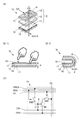
図1は本発明の一態様の検知器10の構成を説明する図である。
FIG. 1 is a diagram illustrating a configuration of a
図2は本発明の一態様の検知器10Bの構成を説明する図である。
FIG. 2 illustrates a structure of the
図3は本発明の一態様の検知器10Bの駆動方法を説明する図である。
FIG. 3 illustrates a method for driving the
図1(A)は本発明の一態様の検知器10の構成を説明する模式図である。
FIG. 1A is a schematic diagram illustrating a structure of a
図1(B−1)および図1(B−2)は検知器10の容量が変化する様子を説明する模式図である。
FIG. 1B-1 and FIG. 1B-2 are schematic diagrams for explaining how the capacitance of the
図1(C)は検知器10に適用することができる検知回路の構成の一例を説明する回路図である。
FIG. 1C is a circuit diagram illustrating an example of a configuration of a detection circuit that can be applied to the
<検知器の構成例1.>
本実施の形態で説明する検知器10は、可視光を透過する窓部14と、窓部14に重なる透光性の検知素子Cと、検知素子Cと電気的に接続される検知回路19と、検知素子Cおよび検知回路19を支持する可撓性の基材16と、を有する(図1(A)参照)。
<Structure example 1 of detector>>
The
そして、検知素子Cは、可撓性の絶縁層13、絶縁層13を挟持する第1の電極11および第2の電極12を備える。
The sensing element C includes a flexible insulating
検知回路19は、検知素子Cの容量の変化に基づいて検知信号DATAを供給する。
The
また、検知器10は、シリコーンゲルを検知素子Cの絶縁層13に含み且つ4mm以上、好ましくは2mm以上、より好ましくは1mm以上の曲率半径で、百回以上、好ましくは千回以上、より好ましくは1万回以上、より好ましくは10万回以上、繰り返し折り曲げることができる構成であってもよい(図1(B−2)参照)。
The
また、検知回路19は、ゲートが検知素子Cの第1の電極11と電気的に接続され、第1の電極が例えば接地電位を供給することができる配線VPIと電気的に接続される第1のトランジスタM1を備える構成であってもよい(図1(C)参照)。
The
また、制御端子が選択信号を供給することができる走査線G1と電気的に接続され、第1の端子が第1のトランジスタM1の第2の電極と電気的に接続され、第2の端子が例えば検知信号DATAを供給することができる信号線DLと電気的に接続される第1のスイッチSW1を備える構成であってもよい。 In addition, the control terminal is electrically connected to the scanning line G1 that can supply a selection signal, the first terminal is electrically connected to the second electrode of the first transistor M1, and the second terminal is For example, the configuration may include a first switch SW1 that is electrically connected to the signal line DL that can supply the detection signal DATA.
また、制御端子がリセット信号を供給することができる配線RESと電気的に接続され、第1の端子が検知素子Cの第1の電極11と電気的に接続され、第2の端子が例えば接地電位を供給することができる配線VRESと電気的に接続される第2のスイッチSW2を備える構成であってもよい。
The control terminal is electrically connected to the wiring RES that can supply a reset signal, the first terminal is electrically connected to the
本実施の形態で説明する検知器10は、可視光を透過する窓部14と、可撓性の絶縁層13およびそれを挟持する一対の電極を備え且つ窓部14に重なる透光性の検知素子Cと、検知素子Cの容量の変化に基づく検知信号DATAを供給する検知回路19と、検知素子Cおよび検知回路19を支持する可撓性の基材16と、を含んで構成される。
The
なお、検知素子Cの容量は、例えば、第1の電極11または第2の電極12にものが近接することもしくは第1の電極11および第2の電極12の間隔dが変化することにより変化する(図1(B−1)参照)。これにより、検知器10は検知素子Cの容量の変化に基づく検知信号DATAを供給すること、可視光を透過することおよび曲げることができる。その結果、利便性または信頼性に優れた新規な検知器を提供することができる。
Note that the capacitance of the sensing element C changes, for example, when an object approaches the
また、検知器10は、検知素子Cの第2の電極12に電気的に接続され且つ検知素子Cの第2の電極の電位を制御することができる制御信号を供給することができる配線CS、検知回路19と電気的に接続され且つ検知信号DATAを供給されることができる信号線DLまたは第2の電極12を支持する可撓性の基材17を含むことができる。
In addition, the
なお、検知器10の第1の電極11、第1のトランジスタM1のゲートおよび第2のスイッチSW2の第1の端子が電気的に接続される結節部をノードAという。
Note that a node where the
以下に、検知器10を構成する個々の要素について説明する。なお、これらの構成は明確に分離できず、一つの構成が他の構成を兼ねる場合や他の構成の一部を含む場合がある。
Below, each element which comprises the
例えば、絶縁性および可撓性を備え第2の電極12を支持する支持体は、絶縁層13であるとともに基材17でもある。
For example, the support body that has insulation and flexibility and supports the
《全体の構成》
検知器10は、窓部14、検知素子C、検知回路19および基材16を有する。
<Overall configuration>
The
また、基材17、信号線DL、配線VPI、配線CS、走査線G1、配線RES、配線VRESおよび信号線DLを有していてもよい。
Further, the
《窓部14》
窓部14は可視光を透過する。これにより検知器10の使用者は、一方の側から他方の側にあるものを視認することができる。例えば、検知器10の一方の側から、他方の側に配置された表示装置が表示する画像情報を視認することができる。
<
The
例えば、可視光を透過する材料または可視光を透過する程度に薄い材料を用いた基材16、第1の電極11、可撓性を有する絶縁層13、基材17および第2の電極12を、可視光の透過を妨げないように重ねて配置して、窓部14を構成すればよい(図1(A)参照)。
For example, the
例えば、可視光を透過しない材料に開口部を設けて用いてもよい。具体的には、矩形などさまざまな形の開口部を1つまたは複数設けて用いてもよい。 For example, an opening may be provided in a material that does not transmit visible light. Specifically, one or a plurality of openings having various shapes such as a rectangle may be provided.
《検知素子C》
検知素子Cは、第1の電極11、第2の電極12および可撓性を有する絶縁層13を有する。
<< Sensing element C >>
The sensing element C includes a
第2の電極12は、第1の電極11と容量を形成するように配置する。例えば、第2の電極12を第1の電極11に重なるように配置してもよく、第2の電極12を第1の電極11に並ぶように配置してもよい。
The
例えば、図1(A)に示す検知素子Cは、第1の電極11と第1の電極11に重なる第2の電極12を備える。
For example, the sensing element C illustrated in FIG. 1A includes a
例えば、大気中に置かれた検知素子Cの第1の電極11または第2の電極12に、大気と異なる誘電率を有するものが近づくと、検知素子Cの容量が変化する。具体的には、指などのものが検知素子Cに近づくと、検知素子Cの容量が変化する(図1(B−1)左参照)。これにより、近接検知器に用いることができる。
For example, when a sensor having a dielectric constant different from that of the atmosphere approaches the
例えば、変形することができる検知素子Cの容量は、変形に伴い変化する。 For example, the capacitance of the sensing element C that can be deformed changes with the deformation.
具体的には、指などのものが検知素子Cに触れることにより、第1の電極11と第2の電極12の間隔dが狭くなると、検知素子Cの容量は大きくなる(図1(B−1)右参照)。これにより、接触検知器に用いることができる。その結果、筆圧を検知することができる。
Specifically, when the distance d between the
具体的には、検知素子Cが折り曲げることができるように可撓性を有する絶縁層13を備える場合、検知素子Cを折り曲げることにより可撓性を有する絶縁層13は圧縮され、第1の電極11と第2の電極12の間隔dが狭くなる。これにより、検知素子Cの容量は大きくなる(図1(B−2)参照)。これにより、屈曲検知器に用いることができる。
Specifically, when the insulating
第1の電極11および第2の電極12は、導電性の材料を含む。
The
例えば、無機導電性材料、有機導電性材料、金属または導電性セラミックスなどを第1の電極11および第2の電極12に用いることができる。
For example, an inorganic conductive material, an organic conductive material, a metal, a conductive ceramic, or the like can be used for the
具体的には、アルミニウム、クロム、銅、タンタル、チタン、モリブデン、タングステン、ニッケル、銀またはマンガンから選ばれた金属元素、上述した金属元素を成分とする合金または上述した金属元素を組み合わせた合金などを用いることができる。 Specifically, a metal element selected from aluminum, chromium, copper, tantalum, titanium, molybdenum, tungsten, nickel, silver or manganese, an alloy containing the above metal element as a component, or an alloy combining the above metal element, etc. Can be used.
具体的には、酸化インジウム、インジウム錫酸化物、インジウム亜鉛酸化物、酸化亜鉛、ガリウムを添加した酸化亜鉛などの導電性酸化物を用いることができる。 Specifically, a conductive oxide such as indium oxide, indium tin oxide, indium zinc oxide, zinc oxide, or zinc oxide to which gallium is added can be used.
具体的には、グラフェンまたはグラファイトを用いることができる。 Specifically, graphene or graphite can be used.
具体的には、導電性高分子を用いることができる。 Specifically, a conductive polymer can be used.
《絶縁層13》
絶縁層13は大きな体積抵抗率を備える。例えば、1×10¹⁴以上、好ましくは2×10¹⁴以上、より好ましくは4×10¹⁴以上の体積抵抗率を備える。
<< Insulating
The insulating
10μm以上3000μ以下、好ましくは10μm以上1000μ以下の厚さを有する材料を、絶縁層13に用いることができる。
A material having a thickness of 10 μm to 3000 μm, preferably 10 μm to 1000 μm can be used for the insulating
絶縁層13は可撓性を有する。例えば、50KPa以下、好ましくは30KPa以下、より好ましくは15KPa以下のヤング率を備える。また、100以上、好ましくは150以上より好ましくは200以上の1/10mmの針入度を備える。また、250%以上、好ましくは340%以上より好ましくは380%以上の伸びを有する。
The insulating
弾性体を絶縁層13に用いることができる。例えば、シリコーンゲルまたは低分子シロキサンを含むシリコーンゲルを用いることができる。
An elastic body can be used for the insulating
《検知回路19》
検知回路19はトランジスタM1ならびに第1のスイッチSW1および第2のスイッチSW2を含む。また、検知回路19は電源電位および信号を供給する配線を含む。例えば、信号線DL、配線VPI、配線CS、走査線G1、配線RES、配線VRESおよび信号線DLなどを含む。
<<
The
なお、窓部14と重ならない領域に検知回路19を配置してもよい。例えば、窓部14と重ならない領域に配線を配置することにより、検知器10の一方の側から他方の側にあるものを視認し易くできる。
Note that the
例えば、トランジスタM1と同一の工程で形成することができるトランジスタを第1のスイッチSW1および第2のスイッチSW2に用いることができる。 For example, a transistor that can be formed in the same process as the transistor M1 can be used for the first switch SW1 and the second switch SW2.
トランジスタM1は半導体層を有する。例えば、4族の元素、化合物半導体または酸化物半導体を半導体層に用いることができる。具体的には、シリコンを含む半導体、ガリウムヒ素を含む半導体またはインジウムを含む酸化物半導体などを適用できる。 The transistor M1 has a semiconductor layer. For example, a Group 4 element, a compound semiconductor, or an oxide semiconductor can be used for the semiconductor layer. Specifically, a semiconductor containing silicon, a semiconductor containing gallium arsenide, an oxide semiconductor containing indium, or the like can be used.
なお、酸化物半導体を半導体層に適用したトランジスタの構成を、実施の形態5において詳細に説明する。
Note that the structure of a transistor in which an oxide semiconductor is used for a semiconductor layer is described in detail in
導電性を有する材料を配線に適用できる。 A conductive material can be applied to the wiring.
例えば、無機導電性材料、有機導電性材料、金属または導電性セラミックスなどを配線に用いることができる。具体的には、第1の電極11および第2の電極12に用いることができる材料を適用できる。
For example, an inorganic conductive material, an organic conductive material, a metal, a conductive ceramic, or the like can be used for the wiring. Specifically, a material that can be used for the
基材16に形成した膜を加工して、基材16に検知回路19を形成してもよい。
The
または、検知回路19を他の基材に形成し、他の基材に形成された検知回路19を基材16に転置してもよい。
Alternatively, the
なお、検知回路19を含む検知器10の作製方法を、実施の形態6において詳細に説明する。
A method for manufacturing the
《基材16》
有機材料、無機材料または有機材料と無機材料の複合材料を基材16に用いることができる。
<<
An organic material, an inorganic material, or a composite material of an organic material and an inorganic material can be used for the
5μm以上2500μm以下、好ましくは5μm以上680μm以下、より好ましくは5μm以上170μm以下、より好ましくは5μm以上45μm以下、より好ましくは8μm以上25μm以下の厚さを有する材料を、基材16に用いることができる。
A material having a thickness of 5 μm to 2500 μm, preferably 5 μm to 680 μm, more preferably 5 μm to 170 μm, more preferably 5 μm to 45 μm, more preferably 8 μm to 25 μm is used for the
また、不純物の透過が抑制された材料を基材16に好適に用いることができる。例えば、水蒸気の透過率が10−5g/(m2・day)以下、好ましくは10−6g/(m2・day)以下である材料を好適に用いることができる。
Further, a material in which the permeation of impurities is suppressed can be suitably used for the
また、線膨張率がおよそ等しい材料を基材16に好適に用いることができる。例えば、線膨張率が1×10⁻³/K以下、好ましくは5×10−5/K以下、より好ましくは1×10−5/K以下である材料を好適に用いることができる。
Further, a material having approximately the same linear expansion coefficient can be suitably used for the
例えば、樹脂、樹脂フィルムまたはプラスチックフィルム等の有機材料を、基材16に用いることができる。
For example, an organic material such as a resin, a resin film, or a plastic film can be used for the
例えば、金属板または厚さ10μm以上50μm以下の薄板状のガラス板等の無機材料を、基材16に用いることができる。
For example, an inorganic material such as a metal plate or a thin glass plate having a thickness of 10 μm to 50 μm can be used for the
例えば、金属板、薄板状のガラス板または無機材料の膜を樹脂フィルム等に貼り合せた複合材料を、基材16に用いることができる。
For example, a composite material in which a metal plate, a thin glass plate, or an inorganic material film is bonded to a resin film or the like can be used for the
例えば、繊維状または粒子状の金属、ガラスもしくは無機材料を樹脂フィルムに分散した複合材料を、基材16に用いることができる。
For example, a composite material in which a fibrous or particulate metal, glass, or inorganic material is dispersed in a resin film can be used for the
具体的には、ポリエステル、ポリオレフィン、ポリアミド、ポリイミド、ポリカーボネート若しくはアクリル樹脂等の樹脂フィルムまたは樹脂板を用いることができる。 Specifically, a resin film or a resin plate such as polyester, polyolefin, polyamide, polyimide, polycarbonate, or acrylic resin can be used.
具体的には、無アルカリガラス、ソーダ石灰ガラス、カリガラス若しくはクリスタルガラス等を用いることができる。 Specifically, alkali-free glass, soda-lime glass, potash glass, crystal glass, or the like can be used.
具体的には、金属酸化物膜、金属窒化物膜若しくは金属酸窒化物膜等を用いることができる。例えば、酸化珪素、窒化珪素、酸窒化珪素、アルミナ膜等を適用できる。 Specifically, a metal oxide film, a metal nitride film, a metal oxynitride film, or the like can be used. For example, silicon oxide, silicon nitride, silicon oxynitride, an alumina film, or the like can be applied.
具体的には、SUSまたはアルミニウム等を用いることができる。 Specifically, SUS or aluminum can be used.
<検知器の構成例2.>
本発明の一態様の検知器の別の構成について、図2を参照しながら説明する。
<Configuration Example 2 of Detector>>
Another structure of the detector of one embodiment of the present invention is described with reference to FIG.
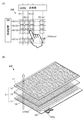
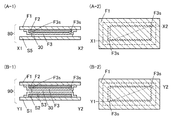
図2(A)は本発明の一態様の検知器10Bの底面を説明する模式図および回路図である。なお、均等に図中に配置された破線と黒丸は、矩形の領域が繰り返し配置されている旨を省略して図示するものである。
FIG. 2A is a schematic diagram and a circuit diagram illustrating a bottom surface of the
図2(B)は図2(A)に破線の円で囲まれた部分の矩形の領域の詳細な底面図である。 FIG. 2B is a detailed bottom view of a rectangular region surrounded by a broken-line circle in FIG.
図2(C)は図2(A)に記号で示すトランジスタM1を含む部分の底面図である。 FIG. 2C is a bottom view of a portion including the transistor M1 indicated by a symbol in FIG.
図2(D)は図2(C)に示す切断線X1−X2および切断線Y1−Y2における断面の構造を説明する断面図である。 2D is a cross-sectional view illustrating a structure of a cross section along the cutting line X1-X2 and the cutting line Y1-Y2 illustrated in FIG.
本実施の形態で説明する検知器10Bは、可視光を透過する窓部14と、窓部14に重なり且つ所定の色の光を透過する着色層と、窓部14を囲む遮光性の層BMと、窓部14に重なる検知素子Cと、遮光性の層BMに重なり検知素子Cと電気的に接続される検知回路19と、検知素子Cおよび検知回路19を支持する可撓性の基材16と、を有する(図2(A)乃至図2(D)参照)。
The
そして、検知素子Cは、可撓性の絶縁層13、絶縁層13を挟持する第1の電極11および第2の電極12を備える。
The sensing element C includes a flexible insulating
検知回路19は、検知素子Cの容量の変化に基づいて検知信号DATAを供給する。
The
また、検知回路19は、ゲートが検知素子Cの第1の電極11と電気的に接続され、第1の電極が例えば接地電位を供給することができる配線VPIと電気的に接続される第1のトランジスタM1を備える構成であってもよい(図2(A)参照)。
The
また、ゲートが選択信号を供給することができる走査線G1と電気的に接続され、第1の電極が第1のトランジスタM1の第2の電極と電気的に接続され、第2の電極が例えば検知信号DATAを供給することができる信号線DLと電気的に接続される第2のトランジスタM2を備える構成であってもよい。 Further, the gate is electrically connected to the scanning line G1 that can supply a selection signal, the first electrode is electrically connected to the second electrode of the first transistor M1, and the second electrode is, for example, The configuration may include a second transistor M2 that is electrically connected to the signal line DL that can supply the detection signal DATA.
また、ゲートがリセット信号を供給することができる配線RESと電気的に接続され、第1の電極が検知素子Cの第1の電極11と電気的に接続され、第2の電極が例えば接地電位を供給することができる配線VRESと電気的に接続される第3のトランジスタM3を備える構成であってもよい。
Further, the gate is electrically connected to the wiring RES that can supply a reset signal, the first electrode is electrically connected to the
また、検知素子Cの第2の電極12と電気的に接続され且つ第2の電極の電位を制御することができる制御信号を供給することができる配線CSを備える構成であってもよい。
In addition, the configuration may include a wiring CS that is electrically connected to the
本実施の形態で説明する検知器10Bは、窓部14と、窓部14に重なり且つ所定の色の可視光を透過する着色層と、窓部14を囲む遮光性の層BMと、可撓性の絶縁層13およびそれを挟持する一対の電極を備え且つ窓部14に重なる透光性の検知素子Cと、遮光性の層BMに重なり検知素子Cの容量の変化に基づく検知信号DATAを供給する検知回路19と、検知素子Cおよび検知回路19を支持する可撓性の基材16と、を含んで構成される。
The
なお、検知素子Cの容量は、例えば、第1の電極11または第2の電極12にものが近接すること、もしくは第1の電極11および第2の電極12の間隔が変化することにより変化する。これにより、検知器10は検知素子Cの容量の変化に基づく検知信号DATAを供給すること、可視光を透過することおよび曲げることができる。その結果、利便性または信頼性に優れた新規な検知器を提供することができる。
Note that the capacitance of the sensing element C changes, for example, when an object is close to the
なお、配線VRESおよび配線VPIは例えば接地電位を供給することができ、配線VPOおよび配線BRは例えば高電源電位を供給することができる。 Note that the wiring VRES and the wiring VPI can supply, for example, a ground potential, and the wiring VPO and the wiring BR can supply, for example, a high power supply potential.
また、配線RESはリセット信号を供給することができ、走査線G1は選択信号を供給することができ、配線CSは検知素子の第2の電極12の電位を制御する制御信号を供給することができる。
The wiring RES can supply a reset signal, the scanning line G1 can supply a selection signal, and the wiring CS can supply a control signal for controlling the potential of the
また、信号線DLは検知信号DATAを供給することができ、端子OUTは検知信号DATAに基づいて変換された信号を供給することができる。 The signal line DL can supply the detection signal DATA, and the terminal OUT can supply a signal converted based on the detection signal DATA.
本実施の形態で説明する検知器10Bは、窓部14に重なり所定の色の光を透過する着色層を備える点、窓部14を囲む遮光性の層BMを備える点、遮光性の層BMに重なる位置に配置される検知回路19を備える点、第1のスイッチにとして第2のトランジスタを備える点、第2のスイッチとして第3のトランジスタを備える点が、図1を参照しながら説明する検知器10とは異なる。ここでは異なる構成について詳細に説明し、同様の構成を用いることができる部分は、上記の説明を援用する。
The
以下に、検知器10Bを構成する個々の要素について説明する。なお、これらの構成は明確に分離できず、一つの構成が他の構成を兼ねる場合や他の構成の一部を含む場合がある。
Below, each element which comprises
《窓部、着色層および遮光性の層》
窓部14は可視光を透過する。
<< Window, colored layer and light-shielding layer >>
The
窓部14に重なる位置に所定の色の光を透過する着色層を備える。例えば、青色の光を透過する着色層CFB、着色層CFGまたは着色層CFRを備える(図2(B)乃至図2(D)参照)。
A colored layer that transmits light of a predetermined color is provided at a position overlapping the
なお、青色、緑色または/および赤色に加えて、白色の光を透過する着色層または黄色の光を透過する着色層などさまざまな色の光を透過する着色層を備えることができる。 In addition to blue, green, and / or red, a colored layer that transmits light of various colors such as a colored layer that transmits white light or a colored layer that transmits yellow light can be provided.
金属材料、顔料または染料等を着色層に用いることができる。 Metal materials, pigments or dyes can be used for the colored layer.
なお、着色層および遮光性の層BMを覆う透光性のオーバーコート層を備えることができる。 Note that a light-transmitting overcoat layer covering the colored layer and the light-shielding layer BM can be provided.
窓部14を囲む遮光性の層BMを備える。遮光性の層BMは窓部14より光を透過しにくい。
A light-shielding layer BM surrounding the
カーボンブラック、金属酸化物、複数の金属酸化物の固溶体を含む複合酸化物等を遮光性の層BMに用いることができる。 Carbon black, a metal oxide, a composite oxide containing a solid solution of a plurality of metal oxides, or the like can be used for the light-shielding layer BM.
《検知回路および配線》
検知回路19および配線を遮光性の層BMに重なる位置に備える構成が好ましい。
<< Detection circuit and wiring >>
A configuration in which the
第1のトランジスタM1と同一の工程で形成することができるトランジスタを、第2のトランジスタM2および第3のトランジスタM3に用いることができる。 A transistor that can be formed in the same process as the first transistor M1 can be used as the second transistor M2 and the third transistor M3.
また、遮光性の層BMに重なるように配線を配置する場合、可視光を透過しにくい材料を配線に用いることができる。例えば、透光性を有する導電膜と比較して優れた導電性を有する材料を用いることができる。具体的には、金属を用いることができる。 Further, when the wiring is arranged so as to overlap with the light-shielding layer BM, a material that hardly transmits visible light can be used for the wiring. For example, a material having superior conductivity compared to a light-transmitting conductive film can be used. Specifically, a metal can be used.
基材16に形成した膜を加工して、基材16に検知回路19を形成してもよい。
The
または、検知回路19を他の基材に形成し、他の基材に形成された検知回路19を基材16に転置してもよい。
Alternatively, the
なお、検知回路19を含む検知器の作製方法を、実施の形態6において詳細に説明する。
A method for manufacturing a detector including the
<検知器の駆動方法>
本実施の形態で説明する検知器10Bの駆動方法について、図3を参照しながら説明する。
<Driving method of detector>
A driving method of the
図3(A)は本発明の一態様の検知器10Bおよび変換器CONVの構成を説明する回路図であり、図3(B−1)および図3(B−2)は駆動方法を説明するタイミングチャートである。
FIG. 3A is a circuit diagram illustrating structures of the
なお、検知信号DATAを変換して端子OUTに供給することができるさまざまな回路を、変換器CONVに用いることができる。例えば、変換器CONVを検知回路19と電気的に接続することにより、ソースフォロワ回路またはカレントミラー回路などが構成されるようにしてもよい。
Note that various circuits that can convert the detection signal DATA and supply it to the terminal OUT can be used for the converter CONV. For example, a source follower circuit or a current mirror circuit may be configured by electrically connecting the converter CONV to the
具体的には、トランジスタM4を用いた変換器CONVを用いて、ソースフォロワ回路を構成できる(図3(A)参照)。なお、第1のトランジスタM1乃至第3のトランジスタM3と同一の工程で作製することができるトランジスタをトランジスタM4に用いてもよい。 Specifically, a source follower circuit can be configured using the converter CONV including the transistor M4 (see FIG. 3A). Note that a transistor that can be manufactured in the same process as the first transistor M1 to the third transistor M3 may be used for the transistor M4.
《第1のステップ》
第1のステップにおいて、第3のトランジスタを導通状態にした後に非導通状態にするリセット信号をゲートに供給し、検知素子Cの第1の電極の電位を所定の電位にする(図3(B−1)期間T1参照)。
<< First Step >>
In the first step, a reset signal for turning off the third transistor after turning it on is supplied to the gate, and the potential of the first electrode of the sensing element C is set to a predetermined potential (FIG. 3B -1) Refer to period T1).
具体的には、リセット信号を配線RESに供給させる。リセット信号が供給された第3のトランジスタは、ノードAの電位を例えば接地電位にする(図3(A)参照)。 Specifically, a reset signal is supplied to the wiring RES. The third transistor to which the reset signal is supplied sets the potential of the node A to, for example, the ground potential (see FIG. 3A).
《第2のステップ》
第2のステップにおいて、第2のトランジスタM2を導通状態にする選択信号をゲートに供給し、第1のトランジスタの第2の電極を信号線DLに電気的に接続する。
<< Second Step >>
In the second step, a selection signal for turning on the second transistor M2 is supplied to the gate, and the second electrode of the first transistor is electrically connected to the signal line DL.
具体的には、走査線G1に選択信号を供給させる。選択信号が供給された第2のトランジスタM2は、第1のトランジスタの第2の電極を信号線DLに電気的に接続する(図3(B−1)期間T2参照)。 Specifically, a selection signal is supplied to the scanning line G1. The second transistor M2 to which the selection signal is supplied electrically connects the second electrode of the first transistor to the signal line DL (see period T2 in FIG. 3B-1).
《第3のステップ》
第3のステップにおいて、制御信号を検知素子の第2の電極12に供給し、制御信号および検知素子Cの容量に基づいて変化する電位を第1のトランジスタM1のゲートに供給する。
《Third step》
In the third step, a control signal is supplied to the
具体的には、配線CSに矩形の制御信号を供給させる。矩形の制御信号を第2の電極12に供給された検知素子Cは、検知素子Cの容量に基づいてノードAの電位を上昇する(図3(B−1)期間T2の後半を参照)。
Specifically, a rectangular control signal is supplied to the wiring CS. The sensing element C supplied with the rectangular control signal to the
例えば、検知素子が大気中に置かれている場合、大気より誘電率の高いものが、検知素子Cの第2の電極12に近接して配置された場合、検知素子Cの容量は見かけ上大きくなる。
For example, when the sensing element is placed in the atmosphere, if a sensor having a dielectric constant higher than that of the atmosphere is disposed close to the
これにより、矩形の制御信号がもたらすノードAの電位の変化は、大気より誘電率の高いものが近接して配置されていない場合に比べて小さくなる(図3(B−2)実線参照)。 As a result, the change in potential of the node A caused by the rectangular control signal is smaller than that in the case where those having a dielectric constant higher than that of the atmosphere are not arranged close to each other (see the solid line in FIG. 3B-2).
《第4のステップ》
第4のステップにおいて、第1のトランジスタM1のゲートの電位の変化に基づく信号を、信号線DLに供給する。
<< Fourth Step >>
In the fourth step, a signal based on a change in the potential of the gate of the first transistor M1 is supplied to the signal line DL.
例えば、第1のトランジスタM1のゲートの電位の変化に基づく電流の変化を信号線DLに供給する。 For example, a change in current based on a change in the potential of the gate of the first transistor M1 is supplied to the signal line DL.
変換器CONVは、信号線DLを流れる電流の変化を電圧の変化に変換して供給する。 The converter CONV converts a change in current flowing through the signal line DL into a change in voltage and supplies it.
《第5のステップ》
第5のステップにおいて、第2のトランジスタを非導通状態にする選択信号をゲートに供給する。
<< 5th step >>
In the fifth step, a selection signal for turning off the second transistor is supplied to the gate.
なお、本実施の形態は、本明細書で示す他の実施の形態と適宜組み合わせることができる。 Note that this embodiment can be combined with any of the other embodiments described in this specification as appropriate.
(実施の形態2)
本実施の形態では、本発明の一態様の入力装置の構成について、図4および図5を参照しながら説明する。
(Embodiment 2)
In this embodiment, the structure of the input device of one embodiment of the present invention is described with reference to FIGS.
図4は本発明の一態様の入力装置200の構成を説明する図である。
FIG. 4 illustrates the structure of the
図5は本発明の一態様の入力装置200の駆動方法を説明する図である。
FIG. 5 illustrates a method for driving the
図4(A)は入力装置200の構成を説明するブロック図であり、図4(B)は入力装置200の外観を説明する投影図である。
FIG. 4A is a block diagram illustrating the configuration of the
なお、入力装置200はタッチセンサということもできる。
The
<入力装置の構成例>
本実施の形態で説明する入力装置200は、マトリクス状に配置される複数の検知ユニット10Uと、行方向に配置される複数の検知ユニット10Uが電気的に接続される走査線G1と、列方向に配置される複数の検知ユニット10Uが電気的に接続される信号線DLと、検知ユニット10U、走査線G1および信号線DLが配設される可撓性の基材16と、を有する(図4(A)参照)。
<Configuration example of input device>
The
例えば、複数の検知ユニット10Uをn行m列(nおよびmは1以上の自然数)のマトリクス状に配置することができる。
For example, a plurality of
なお、i行目のj列目(iはn以下の自然数、jはm以下の自然数)に配設される検知ユニット10Uを検知ユニット10U(i,j)と表記する。また、i行目に配設される走査線G1を走査線G1(i)と表記し、j列目に配設される信号線DLを信号線DL(J)と表記する。
The
そして、検知ユニット10Uは、可視光を透過する窓部14(図示せず)、窓部14に重なる検知素子Cおよび検知素子Cと電気的に接続される検知回路19(図示せず)を備える。
The
例えば、実施の形態1で説明する検知器10Bと同様の構成を検知ユニット10Uに適用できる(図2参照)。
For example, the same configuration as the
検知素子Cは、可撓性の絶縁層13、絶縁層13を挟持する第1の電極11および第2の電極12を備える。
The sensing element C includes a flexible insulating
検知回路19は、選択信号を供給され且つ検知素子Cの容量の変化に基づいて検知信号を供給する。
The
走査線G1は、選択信号を供給することができ、信号線DLは、検知信号を供給することができる。 The scanning line G1 can supply a selection signal, and the signal line DL can supply a detection signal.
また、入力装置200は、シリコーンゲルを検知素子Cの絶縁層13に含み且つ4mm以上、好ましくは2mm以上、より好ましくは1mm以上の曲率半径で繰り返し折り曲げることができる構成であってもよい。
The
また、検知回路19は、ゲートが検知素子Cの第1の電極11と電気的に接続され、第1の電極が例えば接地電位を供給することができる配線VPIと電気的に接続される第1のトランジスタM1を備える構成であってもよい(図3(A)参照)。
The
また、ゲートが選択信号を供給することができる走査線G1と電気的に接続され、第1の電極が第1のトランジスタM1の第2の電極と電気的に接続され、第2の電極が例えば検知信号DATAを供給することができる信号線DLと電気的に接続される第2のトランジスタM2を備える構成であってもよい。 Further, the gate is electrically connected to the scanning line G1 that can supply a selection signal, the first electrode is electrically connected to the second electrode of the first transistor M1, and the second electrode is, for example, The configuration may include a second transistor M2 that is electrically connected to the signal line DL that can supply the detection signal DATA.
また、ゲートがリセット信号を供給することができる配線RESと電気的に接続され、第1の電極が検知素子Cの第1の電極と電気的に接続され、第2の電極が例えば接地電位を供給することができる配線VRESと電気的に接続される第3のトランジスタM3を備える構成であってもよい。 Further, the gate is electrically connected to the wiring RES that can supply a reset signal, the first electrode is electrically connected to the first electrode of the sensing element C, and the second electrode has a ground potential, for example. A structure including the third transistor M3 electrically connected to the wiring VRES that can be supplied may be used.
本実施の形態で説明する入力装置200は、可視光を透過する窓部、可撓性の絶縁層およびそれを挟持する一対の電極を備え且つ窓部に重なる透光性の検知素子ならびに検知素子の容量の変化に基づく検知信号を供給する検知回路を含み且つマトリクス状に配置される検知ユニットと、検知ユニットを支持する可撓性の基材を含んで構成される。
An
なお、検知素子の容量は、例えば、第1の電極または第2の電極12にものが近接すること、もしくは第1の電極および第2の電極12の間隔が変化することにより変化する。これにより、入力装置は、検知ユニットの位置情報および当該検知ユニットが検知する検知信号を、供給すること、可視光を透過することおよび曲げることができる。その結果、利便性または信頼性に優れた新規な入力装置を提供することができる。
Note that the capacitance of the sensing element changes when, for example, the first electrode or the
また、入力装置200は、検知素子Cの第2の電極12の面積が、一の信号線に電気的に接続される複数の検知素子Cが備える第1の電極11の面積の和の10倍以上好ましくは20倍以上である。
In the
本実施の形態で説明する入力装置200は、選択信号を用いて一の信号線DLに接続された複数の検知ユニット10Uから一の検知ユニット10Uを選択することができ且つ面積が第2の電極12に比べて十分小さい第1の電極11を含んで構成される。
The
これにより、選択している検知ユニットに由来する容量を、選択していない検知ユニットに由来する容量から分離することができる。また、第1電極の面積が小さい検知ユニットを配置して、位置情報を詳細に取得することができる。また、第1の電極がノイズを拾いにくくなる。その結果、利便性または信頼性に優れた新規な入力装置を提供することができる。 Thereby, the capacity | capacitance originating in the detection unit currently selected can be isolate | separated from the capacity | capacitance originating in the detection unit which is not selected. In addition, the position information can be acquired in detail by arranging a detection unit having a small area of the first electrode. Moreover, it becomes difficult for the first electrode to pick up noise. As a result, a novel input device that is highly convenient or reliable can be provided.
また、入力装置200は選択信号を所定のタイミングで供給することができる駆動回路GDを備えていてもよい。例えば、駆動回路GDは選択信号を走査線ごとに所定の順番で供給する。
The
また、入力装置200は検知ユニット10Uが供給する検知信号DATAを変換する変換器CONVを備えていてもよい。変換器CONVは複数の変換器CONV(1)乃至CONV(j)を備える(jは1以上m以下の自然数)。例えば、変換器CONV(j)は、信号線DL(j)が供給する検知信号DATAを変換して、供給してもよい。
The
また、入力装置200は、フレキシブルプリント基板FPCと電気的に接続されてもよい。例えば、フレキシブルプリント基板FPCは、電源電位などさまざまな電位またはさまざまなタイミング信号などを供給してもよく、検知信号DATAに基づく信号を供給されてもよい。
Further, the
なお、本実施の形態で説明する入力装置は、実施の形態1で説明する検知器10Bと同じ構成を備える検知ユニット10Uを基材16上にマトリクス状に複数備える点、行方向に配置される複数の検知ユニット10Uが電気的に接続される走査線G1を複数備える点、列方向に配置される検知ユニット10Uが電気的に接続される信号線DLを複数備える点、検知ユニット10Uの第1の電極11が第2の電極12に比べて十分小さい点が、図2を参照しながら実施の形態1で説明する検知器10とは異なる。ここでは異なる構成について詳細に説明し、同様の構成を用いることができる部分は、上記の説明を援用する。
Note that the input device described in the present embodiment is arranged in the row direction in that a plurality of
以下に、入力装置200を構成する個々の要素について説明する。なお、これらの構成は明確に分離できず、一つの構成が他の構成を兼ねる場合や他の構成の一部を含む場合がある。
Below, each element which comprises the
《全体の構成》
入力装置200は、複数の検知ユニット10Uと、走査線G1と、信号線DLとを有する。
<Overall configuration>
The
また、駆動回路GDと、変換器CONVと、を有してもよい。 Moreover, you may have the drive circuit GD and the converter CONV.
同一の工程で形成することができるトランジスタを用いて、複数の検知ユニット10Uの検知回路19、駆動回路GDおよび変換器CONVを構成することができる。
The
《走査線および信号線》
走査線G1および信号線DLを、検知ユニット10Uの遮光性の膜BMと重なる位置に配置すると好ましい。
<< Scanning lines and signal lines >>
It is preferable to arrange the scanning line G1 and the signal line DL at a position overlapping the light shielding film BM of the
なお、複数の検知ユニット10Uをストライプ状、モザイク状、デルタ状、ハニカム状またはベイヤ状に基材16に配置してもよい。
A plurality of
《駆動回路GD》
駆動回路GDは、さまざまな組み合わせ回路を用いた論理回路で構成することができる。例えば、シフトレジスタを適用できる。
<< Drive circuit GD >>
The drive circuit GD can be composed of logic circuits using various combinational circuits. For example, a shift register can be applied.
《変換器CONV》
変換器CONVは変換回路を備える。検知信号DATAを変換して供給することができるさまざまな回路を用いることができる。例えば、変換器CONVを検知回路19と電気的に接続することにより、ソースフォロワ回路またはカレントミラー回路などが構成されるようにしてもよい。
<< Converter CONV >>
The converter CONV includes a conversion circuit. Various circuits that can convert and supply the detection signal DATA can be used. For example, a source follower circuit or a current mirror circuit may be configured by electrically connecting the converter CONV to the
<入力装置の駆動方法1.>
本実施の形態で説明する入力装置200の駆動方法について、図5を参照しながら説明する。
<Driving Method of Input Device 1. >
A driving method of the
図5(A)は入力装置200の構成を説明するブロック図であり、図5(B)は入力装置200の駆動方法を説明するタイミングチャートである。
FIG. 5A is a block diagram illustrating a configuration of the
なお、配線VRESおよび配線VPIは例えば接地電位を供給することができ、配線VPOおよび配線BRは例えば高電源電位を供給することができる。 Note that the wiring VRES and the wiring VPI can supply, for example, a ground potential, and the wiring VPO and the wiring BR can supply, for example, a high power supply potential.
また、配線RESはリセット信号を供給することができ、走査線G1は選択信号を供給することができ、配線CSは制御信号を供給することができる。 The wiring RES can supply a reset signal, the scanning line G1 can supply a selection signal, and the wiring CS can supply a control signal.
また、信号線DLは検知信号DATAを供給することができ、端子OUT(j)は検知信号DATAに基づいて変換された信号を供給することができる。 The signal line DL can supply a detection signal DATA, and the terminal OUT (j) can supply a signal converted based on the detection signal DATA.
本実施の形態で説明する入力装置200の駆動方法は、同一のタイミングで一の走査線G1(j)が複数の検知ユニット10Uに選択信号を供給する点および同一のタイミングで複数の端子OUT(j)が検知信号DATAに基づいて変換された信号を供給する点が、図3を参照しながら説明する検知器10の駆動方法とは異なる。ここでは異なるステップについて詳細に説明し、同様のステップを用いることができる部分は、上記の説明を援用する。
In the driving method of the
《第1のステップ》
第1のステップにおいて、リセット信号を供給し、すべての検知ユニット10Uの検知素子Cの第1の電極11の電位を所定の電位にする(図3(A)および図5(B−1)期間T1参照)。例えば、検知素子Cの第1の電極11の電位を接地電位にする。
<< First Step >>
In the first step, a reset signal is supplied to set the potentials of the
また、所定の走査線を順番に選択するように、例えばiの値を1にする。なお、iの値が1であるときを入力フレーム期間の始期ということができる。 For example, the value of i is set to 1 so that predetermined scanning lines are selected in order. Note that the time when the value of i is 1 can be referred to as the start of the input frame period.
《第2のステップ》
第2のステップにおいて、走査線G1(i)を選択し、選択された走査線G1(i)に電気的に接続される検知ユニット10U(i,1)乃至10U(i,m)に選択信号を所定の期間供給する。選択信号が供給された第1のトランジスタの第2の電極を信号線DL(1)乃至DL(m)と電気的に接続する(図3(A)および図5(B−1)期間T2参照)。
<< Second Step >>
In the second step, the scanning line G1 (i) is selected, and selection signals are sent to the
《第3のステップ》
第3のステップにおいて、所定の制御信号を検知素子の第2の電極12に供給し、制御信号および検知素子Cの容量に基づいて変化する電位を第1のトランジスタM1のゲートに供給する。
《Third step》
In the third step, a predetermined control signal is supplied to the
なお、選択信号と同期する信号を制御信号に用いることができる。 Note that a signal synchronized with the selection signal can be used as the control signal.
具体的には、選択信号と同じ周期の矩形波を用いることができる(図5(B−1)参照)。 Specifically, a rectangular wave having the same period as the selection signal can be used (see FIG. 5B-1).
具体的には、選択信号の2倍の周期の矩形波を用いることができる(図5(B−2)参照)。 Specifically, a rectangular wave having a period twice that of the selection signal can be used (see FIG. 5B-2).
矩形の制御信号を第2の電極12に供給された検知素子Cは、検知素子Cの容量に基づいてノードAの電位を上昇する(図5(B−1)期間T2の後半を参照)。
The sensing element C supplied with the rectangular control signal to the
《第4のステップ》
第4のステップにおいて、第1のトランジスタM1のゲートの電位にもたらされる変化に基づいて変化する電流を、信号線DLに供給する。
<< Fourth Step >>
In the fourth step, a current that changes based on a change brought about in the potential of the gate of the first transistor M1 is supplied to the signal line DL.
変換器CONVは、信号線DLを流れる電流の変化を電圧の変化に変換して供給する。 The converter CONV converts a change in current flowing through the signal line DL into a change in voltage and supplies it.
《第5のステップ》
第5のステップにおいて、第2のトランジスタを非導通状態にする選択信号をゲートに供給する。
<< 5th step >>
In the fifth step, a selection signal for turning off the second transistor is supplied to the gate.
《第6のステップ》
第6のステップにおいて、iの値に1を加え、その値がn以下である場合は、第2のステップに進む。
<< Sixth Step >>
In the sixth step, 1 is added to the value of i. If the value is n or less, the process proceeds to the second step.
具体的には、iの値がnより小さい場合は、第2のステップにおいて、走査線G1(i+1)を選択し、選択された走査線G1(i+1)に電気的に接続される検知ユニット10U(i+1,1)乃至10U(i+1,m)に選択信号を所定の期間供給する。選択信号が供給された第1のトランジスタの第2の電極を信号線DL(1)乃至DL(m)と電気的に接続する(図3(A)および図5(B−1)期間T3参照)。
Specifically, when the value of i is smaller than n, in the second step, the scanning line G1 (i + 1) is selected, and the
iの値に1を加えた値がnより大きい場合は、第1のステップに進む。また、iの値に1を加えた値がnより大きいときを入力フレーム期間の終期ということができる。 When the value obtained by adding 1 to the value of i is larger than n, the process proceeds to the first step. The time when the value obtained by adding 1 to the value of i is larger than n can be called the end of the input frame period.
この駆動方法によれば、入力フレーム期間ごとに、すべての検知ユニットが検知信号DATAを供給する。 According to this driving method, every detection unit supplies the detection signal DATA for each input frame period.
例えば、検知信号DATAは、各検知ユニットに近接するものの位置情報を含む。また、あらかじめマトリクス状に配置されている検知ユニットの位置情報は既知である。 For example, the detection signal DATA includes position information of what is close to each detection unit. Further, the position information of the detection units arranged in advance in a matrix is known.
検知信号DATAおよび検知ユニットの位置情報を関連付けることにより、入力装置200は入力フレーム期間ごとに入力装置200に近接するものの位置情報を供給することができる。
By associating the detection signal DATA with the position information of the detection unit, the
具体的には、演算装置を用いて検知信号DATAおよび検知ユニットの位置情報を解析することにより、入力装置200に近接するものの位置情報を、入力期間ごとに知ることができる。
Specifically, by analyzing the detection signal DATA and the position information of the detection unit using an arithmetic device, the position information of the object close to the
<入力装置の駆動方法2.>
本実施の形態で説明する入力装置200の他の駆動方法について、図5(B−3)を参照しながら説明する。
<Driving Method of Input Device 2. >
Another driving method of the
なお、本実施の形態で説明する入力装置の駆動方法は、第1のステップにおいて、検知素子Cの第2の電極12の電位を第1の電位にする制御信号を供給する点、第2のステップにおいて、iの値がn以上2nより小さい場合は、走査線G1((i−n+1)を選択し、検知ユニット10U(i−n+1,1)乃至10U(i−n+1,m)に選択信号を供給する点、第3のステップにおいて、第1の電位または第2の電位が第2の電極12に供給された検知素子Cの容量の変化に基づいて変化する電位を第1のトランジスタM1のゲートに供給する点、第6のステップにおいて、iの値に1を加え、その値がn+1である場合、検知素子の第2の電極12の電位を、第1のステップで与えた第1の電位と異なる第2の電位にする制御信号を供給する点が、上記で説明する駆動方法とは異なる。ここでは異なるステップについて詳細に説明し、同様の構成を用いることができる部分は、上記の説明を援用する。
Note that in the driving method of the input device described in this embodiment, in the first step, a control signal for supplying the potential of the
《第1のステップ》
第1のステップにおいて、リセット信号を供給し、すべての検知ユニット10Uの検知素子Cの第1の電極の電位を所定の電位にする(図3(A)および図5(B−3)期間U1参照)。
<< First Step >>
In the first step, a reset signal is supplied, and the potentials of the first electrodes of the sensing elements C of all the
また、検知素子Cの第2の電極12の電位を第1の電位にする制御信号を供給する。
In addition, a control signal for supplying the potential of the
また、所定の走査線を順番に選択するように、例えばiの値を1にする。なお、iの値が1であるときを入力フレーム期間の始期ということができる。 For example, the value of i is set to 1 so that predetermined scanning lines are selected in order. Note that when the value of i is 1, it can be said that the input frame period starts.
《第2のステップ》
第2のステップにおいて、iの値がnより小さい場合は、走査線G1(i)を選択し、選択された走査線G1(i)に電気的に接続される検知ユニット10U(i,1)乃至10U(i,m)に選択信号を所定の期間供給する。選択信号が供給された第1のトランジスタの第2の電極を信号線DL(1)乃至DL(m)と電気的に接続する。
<< Second Step >>
In the second step, when the value of i is smaller than n, the scanning line G1 (i) is selected, and the
第2のステップにおいて、iの値がn以上2nより小さい場合は、走査線G1((i−n+1)を選択し、選択された走査線G1(i−n+1)に電気的に接続される検知ユニット10U(i−n+1,1)乃至10U(i−n+1,m)に選択信号を所定の期間供給する。選択信号が供給された第1のトランジスタの第2の電極を信号線DL(1)乃至DL(m)と電気的に接続する。
In the second step, when the value of i is not less than n and less than 2n, the scanning line G1 ((i−n + 1) is selected, and the detection is made to be electrically connected to the selected scanning line G1 (i−n + 1). A selection signal is supplied to the
《第3のステップ》
第3のステップにおいて、検知素子Cの容量の変化に基づいて変化する電位を第1のトランジスタM1のゲートに供給する。
《Third step》
In the third step, a potential that changes based on a change in the capacitance of the sensing element C is supplied to the gate of the first transistor M1.
具体的には、検知素子Cの第2の電極12に、第1の電位または第2の電位が供給され、検知素子Cはその容量の変化に基づいてノードAの電位を変化する(図3(A)参照)。
Specifically, the first potential or the second potential is supplied to the
例えば、検知素子が大気中に置かれている場合、大気より誘電率の高いものが、検知素子Cの第2の電極12に近接して配置された場合、検知素子Cの容量は見かけ上大きくなる。
For example, when the sensing element is placed in the atmosphere, if a sensor having a dielectric constant higher than that of the atmosphere is disposed close to the
これにより、ノードAの電位の変化は、大気より誘電率の高いものが近接して配置されていない場合に比べて小さくなる。 As a result, the change in the potential of the node A becomes smaller than that in the case where the one having a dielectric constant higher than that of the atmosphere is not arranged close to the atmosphere.
《第6のステップ》
第6のステップにおいて、iの値に1を加え、その値がn+1である場合、検知素子の第2の電極12の電位を、第1のステップで与えた第1の電位と異なる第2の電位にする制御信号を供給する(図5(B−3)期間U2参照)。
<< Sixth Step >>
In the sixth step, when 1 is added to the value of i and the value is n + 1, the potential of the
また、iの値に1を加えた値が2n以下である場合は、第2のステップに進む。 When the value obtained by adding 1 to the value of i is 2n or less, the process proceeds to the second step.
また、iの値に1を加えた値が2nより大きい場合は、第1のステップに進む。なお、iの値に1を加えた値が2nより大きいときを入力フレーム期間の終期ということができる。 If the value obtained by adding 1 to the value of i is larger than 2n, the process proceeds to the first step. Note that the value obtained by adding 1 to the value of i is greater than 2n can be referred to as the end of the input frame period.
この駆動方法によれば、入力フレーム期間ごとに、すべての検知ユニットが、一組の検知信号DATAと、を供給する。 According to this driving method, every detection unit supplies a set of detection signals DATA for each input frame period.
具体的には、第2の電極12の電位が第1の電位である場合の検知信号DATAと、第2の電位である場合の検知信号DATAと、を供給する。
Specifically, the detection signal DATA when the potential of the
例えば、一組の検知信号DATAの差は、各検知ユニットに近接するものの位置情報を含む。また、あらかじめマトリクス状に配置されている検知ユニットの位置情報は既知である。 For example, the difference between the set of detection signals DATA includes position information of what is close to each detection unit. Further, the position information of the detection units arranged in advance in a matrix is known.
一組の検知信号DATAの差および検知ユニットの位置情報を関連付けることにより、入力装置200は入力フレーム期間ごとに入力装置200に近接するものの位置情報を供給することができる。
By associating the difference between the set of detection signals DATA and the position information of the detection unit, the
具体的には、演算装置を用いて一組の検知信号DATAの差および検知ユニットの位置情報を解析することにより、入力装置200に近接するものの位置情報を、入力期間ごとに知ることができる。
Specifically, by analyzing the difference between the set of detection signals DATA and the position information of the detection unit using an arithmetic device, the position information of the object close to the
なお、本実施の形態は、本明細書で示す他の実施の形態と適宜組み合わせることができる。 Note that this embodiment can be combined with any of the other embodiments described in this specification as appropriate.
(実施の形態3)
本実施の形態では、本発明の一態様の入出力装置の構成について、図6および図7を参照しながら説明する。
(Embodiment 3)
In this embodiment, the structure of the input / output device of one embodiment of the present invention is described with reference to FIGS.
図6は本発明の一態様の入出力装置の構成を説明する投影図である。 FIG. 6 is a projection view illustrating the structure of the input / output device of one embodiment of the present invention.
図6(A)は本発明の一態様の入出力装置500の投影図であり、図6(B)は入出力装置500が備える検知ユニット10Uの構成を説明する投影図である。
6A is a projection view of the input /
図7は本発明の一態様の入出力装置500の構成を説明する断面図である。
FIG. 7 is a cross-sectional view illustrating the structure of the input /
図7(A)は図6に示す本発明の一態様の入出力装置500のZ1−Z2における断面図である。
FIG. 7A is a cross-sectional view taken along Z1-Z2 of the input /
なお、入出力装置500はタッチパネルということもできる。
Note that the input /
<入出力装置の構成例>
本実施の形態で説明する入出力装置500は、可視光を透過する窓部14を具備し且つマトリクス状に配設される複数の検知ユニット10U、行方向(図中に矢印Rで示す)に配置される複数の検知ユニット10Uが電気的に接続される走査線G1、列方向(図中に矢印Cで示す)に配置される複数の検知ユニット10Uが電気的に接続される信号線DLならびに、検知ユニット10U、走査線G1および信号線DLを支持する可撓性の第1の基材16を備える可撓性の入力装置200と、マトリクス状に配設され且つ窓部14に重なる複数の画素502および画素502を支持する可撓性の第2の基材510を備える表示部501と、を有する(図6(A)乃至図6(C)参照)。
<Configuration example of input / output device>
The input /
検知ユニット10Uは、窓部14に重なる検知素子Cおよび検知素子Cと電気的に接続される検知回路19を備える(図6(B)参照)。
The
検知素子Cは、可撓性の絶縁層13、絶縁層13を挟持する第1の電極11および第2の電極12を備える。
The sensing element C includes a flexible insulating
検知回路19は、選択信号を供給され且つ検知素子Cの容量の変化に基づいて検知信号DATAを供給する。
The
検知回路19は、選択信号を供給され且つ検知素子Cの容量の変化に基づいて検知信号DATAを供給する。
The
走査線G1は、選択信号を供給することができ、信号線DLは、検知信号DATAを供給することができ、検知回路19は、複数の窓部14の間隙に重なるように配置される。
The scanning line G1 can supply a selection signal, the signal line DL can supply a detection signal DATA, and the
また、本実施の形態で説明する入出力装置500は、検知ユニット10Uおよび検知ユニット10Uの窓部14と重なる画素502の間に、着色層を備える。
The input /
本実施の形態で説明する入出力装置500は、可視光を透過する窓部14を具備する検知ユニット10Uを複数備える可撓性の入力装置200と、窓部14に重なる画素502を複数備える可撓性の表示部501と、を有し、窓部14と画素502の間に着色層を含んで構成される。
The input /
これにより、入出力装置は容量の変化に基づく検知信号およびそれを供給する検知ユニットの位置情報を供給すること、検知ユニットの位置情報と関連付けられた画像情報を表示することならびに曲げることができる。その結果、利便性または信頼性に優れた新規な入出力装置を提供することができる。 Accordingly, the input / output device can supply the detection signal based on the change in the capacity and the position information of the detection unit that supplies the detection signal, display the image information associated with the position information of the detection unit, and bend it. As a result, a novel input / output device that is highly convenient or reliable can be provided.
また、入出力装置500は、入力装置200が供給する信号を供給されるフレキシブルプリント基板FPC1または/および画像情報を含む信号を表示部501に供給するフレキシブルプリント基板FPC2を備えていてもよい。
The input /
また、傷の発生を防いで入出力装置500を保護する保護層17pまたは/および入出力装置500が反射する外光の強度を弱める反射防止層567pを備えていてもよい。
Further, a
また、入出力装置500は、表示部501の信号線に画像線信号を供給する信号線駆動回路503s、信号を供給する配線511およびフレキシブルプリント基板FPC2と電気的に接続される端子519を有する。
In addition, the input /
以下に、入出力装置500を構成する個々の要素について説明する。なお、これらの構成は明確に分離できず、一つの構成が他の構成を兼ねる場合や他の構成の一部を含む場合がある。
Hereinafter, individual elements constituting the input /
例えば、複数の窓部14に重なる位置に着色層を備える入力装置200は、入力装置200であるとともにカラーフィルタでもある。
For example, the
また、例えば入力装置200が表示部501に重ねられた入出力装置500は、入力装置200であるとともに表示部501でもある。
For example, the input /
《全体の構成》
入出力装置500は、入力装置200と、表示部501と、を備える(図6(A)参照)。
<Overall configuration>
The input /
《入力装置200》
入力装置200は複数の検知ユニット10Uおよび検知ユニットを支持する可撓性の基材16を備える。
<<
The
例えば、40行15列のマトリクス状に複数の検知ユニット10Uを可撓性の基材16に配設する。また、検知ユニットの大きさを幅7.668mm高さ5.112mmの大きさにしてもよい。
For example, the plurality of
《窓部14、着色層および遮光性の層BM》
窓部14は可視光を透過する。
<<
The
窓部14に重なる位置に所定の色の光を透過する着色層を備える。例えば、青色の光を透過する着色層CFB、着色層CFGまたは着色層CFRを備える(図6(B)参照)。
A colored layer that transmits light of a predetermined color is provided at a position overlapping the
なお、青色、緑色または/および赤色に加えて、白色の光を透過する着色層または黄色の光を透過する着色層などさまざまな色の光を透過する着色層を備えることができる。 In addition to blue, green, and / or red, a colored layer that transmits light of various colors such as a colored layer that transmits white light or a colored layer that transmits yellow light can be provided.
着色層に金属材料、顔料または染料等を用いることができる。 A metal material, a pigment, a dye, or the like can be used for the colored layer.
窓部14を囲むように遮光性の層BMを備える。遮光性の層BMは窓部14より光を透過しにくい。
A light-shielding layer BM is provided so as to surround the
カーボンブラック、金属酸化物、複数の金属酸化物の固溶体を含む複合酸化物等を遮光性の層BMに用いることができる。 Carbon black, a metal oxide, a composite oxide containing a solid solution of a plurality of metal oxides, or the like can be used for the light-shielding layer BM.
遮光性の層BMと重なる位置に走査線G1、信号線DL、配線VPI、配線RESおよび配線VRESならびに検知回路19を備える。
The scanning line G1, the signal line DL, the wiring VPI, the wiring RES and the wiring VRES, and the
なお、着色層および遮光性の層BMを覆う透光性のオーバーコート層を備えることができる。 Note that a light-transmitting overcoat layer covering the colored layer and the light-shielding layer BM can be provided.
《検知素子C》
検知素子Cは、第1の電極11、第2の電極12および第1の電極11および第2の電極12の間に可撓性を有する絶縁層13を有する(図7(A)参照)。
<< Sensing element C >>
The sensing element C includes a flexible insulating
第1の電極11は他の領域から分離されるように、例えば島状に形成される。特に、入出力装置500の使用者に第1の電極11が識別されないように、第1の電極11と同一の工程で作製することができる層を第1の電極11に近接して配置する構成が好ましい。より好ましくは、第1の電極11および第1の電極11に近接して配置する層の間隙に配置する窓部14の数をできるだけ少なくするとよい。特に、当該間隙に窓部14を配置しない構成が好ましい。なお、第1の電極11の大きさは検知ユニットの大きさとおよそ等しくできる。
The
第1の電極11と重なるように第2の電極12を備え、第1の電極11と第2の電極12の間に絶縁層13を備える。
A
なお、第1の電極の面積を、第2の電極の面積より小さくすることができる。例えば、第2の電極の面積を、一の信号線DLに電気的に接続された列方向に並ぶ複数の検知ユニットが備える第1の電極の面積の和の0.8倍以上にする。 Note that the area of the first electrode can be smaller than the area of the second electrode. For example, the area of the second electrode is set to 0.8 times or more the sum of the areas of the first electrodes provided in the plurality of detection units arranged in the column direction electrically connected to the one signal line DL.
例えば、大気中に置かれた検知素子Cの第1の電極11または第2の電極12に、大気と異なる誘電率を有するものが近づくと、検知素子Cの容量が変化する。具体的には、指などのものが検知素子Cに近づくと、検知素子Cの容量が変化する。これにより、近接検知器に用いることができる。
For example, when a sensor having a dielectric constant different from that of the atmosphere approaches the
例えば、変形することができ、変形に伴い容量が変化する容量素子を、検知素子Cに用いることができる。 For example, a capacitive element that can be deformed and whose capacitance changes with the deformation can be used for the sensing element C.
具体的には、指などのものが検知素子Cに触れることにより、第1の電極11と第2の電極12の間隔が狭くなる容量素子Cを用いることができる。第1の電極11と第2の電極12の間隔が狭くなると、検知素子Cの容量は大きくなる。これにより、接触検知器に用いることができる。
Specifically, it is possible to use the capacitor element C in which the distance between the
具体的には、検知素子Cを折り曲げることにより、第1の電極11と第2の電極12の間隔が狭くなる。これにより、検知素子Cの容量は大きくなる。これにより、屈曲検知器に用いることができる。
Specifically, the distance between the
導電性の材料を、第1の電極11および第2の電極12に用いることができる。
A conductive material can be used for the
例えば、無機導電性材料、有機導電性材料、金属または導電性セラミックスなどを第1の電極11および第2の電極12に用いることができる。
For example, an inorganic conductive material, an organic conductive material, a metal, a conductive ceramic, or the like can be used for the
具体的には、アルミニウム、クロム、銅、タンタル、チタン、モリブデン、タングステン、ニッケル、銀またはマンガンから選ばれた金属元素、上述した金属元素を成分とする合金または上述した金属元素を組み合わせた合金などを用いることができる。 Specifically, a metal element selected from aluminum, chromium, copper, tantalum, titanium, molybdenum, tungsten, nickel, silver or manganese, an alloy containing the above metal element as a component, or an alloy combining the above metal element, etc. Can be used.
または、酸化インジウム、インジウム錫酸化物、インジウム亜鉛酸化物、酸化亜鉛、ガリウムを添加した酸化亜鉛などの導電性酸化物を用いることができる。 Alternatively, a conductive oxide such as indium oxide, indium tin oxide, indium zinc oxide, zinc oxide, or zinc oxide to which gallium is added can be used.
または、グラフェンまたはグラファイトを用いることができる。グラフェンを含む膜は、例えば膜状に形成された酸化グラフェンを含む膜に含まれる酸化グラフェンを還元して形成することができる。還元する方法としては、熱を加える方法や還元剤を用いる方法等を挙げることができる。 Alternatively, graphene or graphite can be used. The film containing graphene can be formed, for example, by reducing graphene oxide contained in a film containing graphene oxide formed in a film shape. Examples of the reduction method include a method of applying heat and a method of using a reducing agent.
または、導電性高分子を用いることができる。 Alternatively, a conductive polymer can be used.
《検知回路19》
検知回路19は例えばトランジスタM1乃至トランジスタM3を含む。また、検知回路19は電源電位および信号を供給する配線を含む。例えば、配線VPI、配線CS、走査線G1、配線RES、配線VRESおよび信号線DLなどを含む。
<<
The
なお、検知回路19の具体的な構成は実施の形態2で詳細に説明する。
The specific configuration of the
なお、検知回路19を窓部14と重ならない領域に配置してもよい。例えば、窓部14と重ならない領域に配線を配置することにより、検知器10の一方の側から他方の側にあるものを視認し易くできる。
Note that the
例えば、同一の工程で形成することができるトランジスタをトランジスタM1乃至トランジスタM3に用いることができる。 For example, transistors that can be formed in the same process can be used as the transistors M1 to M3.
トランジスタM1は半導体層を有する。例えば、4族の元素、化合物半導体または酸化物半導体を半導体層に用いることができる。具体的には、シリコンを含む半導体、ガリウムヒ素を含む半導体またはインジウムを含む酸化物半導体などを適用できる。また、半導体は、単結晶、多結晶もしくは非晶質またはこれらのうちのいずれかを含む混合物であってもよい。 The transistor M1 has a semiconductor layer. For example, a Group 4 element, a compound semiconductor, or an oxide semiconductor can be used for the semiconductor layer. Specifically, a semiconductor containing silicon, a semiconductor containing gallium arsenide, an oxide semiconductor containing indium, or the like can be used. Further, the semiconductor may be single crystal, polycrystalline, amorphous, or a mixture containing any of these.
なお、酸化物半導体を半導体層に適用したトランジスタの構成を、実施の形態5において詳細に説明する。
Note that the structure of a transistor in which an oxide semiconductor is used for a semiconductor layer is described in detail in
導電性を有する材料を配線に適用できる。 A conductive material can be applied to the wiring.
例えば、無機導電性材料、有機導電性材料、金属または導電性セラミックスなどを配線に用いることができる。具体的には、第1の電極11および第2の電極12に用いることができる材料と同一の材料を適用できる。
For example, an inorganic conductive material, an organic conductive material, a metal, a conductive ceramic, or the like can be used for the wiring. Specifically, the same material that can be used for the
アルミニウム、金、白金、銀、ニッケル、チタン、タングステン、クロム、モリブデン、鉄、コバルト、銅、又はパラジウム等の金属材料や、該金属材料を含む合金材料を走査線G1、信号線DL、配線VPI、配線RESおよび配線VRESに用いることができる。 A metal material such as aluminum, gold, platinum, silver, nickel, titanium, tungsten, chromium, molybdenum, iron, cobalt, copper, or palladium, or an alloy material containing the metal material is used as the scan line G1, the signal line DL, and the wiring VPI. The wiring RES and the wiring VRES can be used.
基材16に形成した膜を加工して、基材16に検知回路19を形成してもよい。
The
または、他の基材に形成した検知回路19を基材16に転置してもよい。
Alternatively, the
《基材16》
有機材料、無機材料または有機材料と無機材料の複合材料を可撓性の基材16に用いることができる。
<<
An organic material, an inorganic material, or a composite material of an organic material and an inorganic material can be used for the
5μm以上2500μm以下、好ましくは5μm以上680μm以下、より好ましくは5μm以上170μm以下、より好ましくは5μm以上45μm以下、より好ましくは8μm以上25μm以下の厚さを有する材料を、基材16に用いることができる。
A material having a thickness of 5 μm to 2500 μm, preferably 5 μm to 680 μm, more preferably 5 μm to 170 μm, more preferably 5 μm to 45 μm, more preferably 8 μm to 25 μm is used for the
また、不純物の透過が抑制された材料を基材16に好適に用いることができる。例えば、水蒸気の透過率が10−5g/(m2・day)以下、好ましくは10−6g/(m2・day)以下である材料を好適に用いることができる。
Further, a material in which the permeation of impurities is suppressed can be suitably used for the
また、線膨張率がおよそ等しい材料を基材16に好適に用いることができる。例えば、線膨張率が1×10⁻³/K以下、好ましくは5×10−5/K以下、より好ましくは1×10−5/K以下である材料を好適に用いることができる。
Further, a material having approximately the same linear expansion coefficient can be suitably used for the
例えば、樹脂、樹脂フィルムまたはプラスチックフィルム等の有機材料を、基材16に用いることができる。
For example, an organic material such as a resin, a resin film, or a plastic film can be used for the
例えば、金属板または厚さ10μm以上50μm以下の薄板状のガラス板等の無機材料を、基材16に用いることができる。
For example, an inorganic material such as a metal plate or a thin glass plate having a thickness of 10 μm to 50 μm can be used for the
例えば、金属板、薄板状のガラス板または無機材料の膜を、樹脂層を用いて樹脂フィルム等に貼り合せて形成された複合材料を、基材16に用いることができる。
For example, a composite material formed by bonding a metal plate, a thin glass plate, or an inorganic material film to a resin film or the like using a resin layer can be used for the
例えば、繊維状または粒子状の金属、ガラスもしくは無機材料を樹脂または樹脂フィルムに分散した複合材料を、基材16に用いることができる。
For example, a composite material in which a fibrous or particulate metal, glass, or inorganic material is dispersed in a resin or a resin film can be used for the
例えば、熱硬化性樹脂や紫外線硬化樹脂を樹脂層に用いることができる。 For example, a thermosetting resin or an ultraviolet curable resin can be used for the resin layer.
具体的には、ポリエステル、ポリオレフィン、ポリアミド、ポリイミド、ポリカーボネート若しくはアクリル樹脂等の樹脂フィルムまたは樹脂板を用いることができる。 Specifically, a resin film or a resin plate such as polyester, polyolefin, polyamide, polyimide, polycarbonate, or acrylic resin can be used.
具体的には、無アルカリガラス、ソーダ石灰ガラス、カリガラス若しくはクリスタルガラス等を用いることができる。 Specifically, alkali-free glass, soda-lime glass, potash glass, crystal glass, or the like can be used.
具体的には、金属酸化物膜、金属窒化物膜若しくは金属酸窒化物膜等を用いることができる。例えば、酸化珪素、窒化珪素、酸窒化珪素、アルミナ膜等を適用できる。 Specifically, a metal oxide film, a metal nitride film, a metal oxynitride film, or the like can be used. For example, silicon oxide, silicon nitride, silicon oxynitride, an alumina film, or the like can be applied.
具体的には、開口部が設けられたSUSまたはアルミニウム等を用いることができる。 Specifically, SUS or aluminum provided with an opening can be used.
具体的には、アクリル、ウレタン、エポキシ、またはシロキサン結合を有する樹脂などの樹脂を用いることができる。 Specifically, a resin such as an acrylic resin, a urethane resin, an epoxy resin, or a resin having a siloxane bond can be used.
例えば、可撓性を有する基材16bと、不純物の拡散を防ぐバリア膜16aと、基材16bおよびバリア膜16aを貼り合わせる樹脂層16cと、が積層された積層体を基材16に好適に用いることができる(図7(A)参照)。
For example, a laminate in which a
具体的には、600nmの酸化窒化珪素膜および厚さ200nmの窒化珪素膜が積層された積層材料を含む膜を、バリア膜16aに用いることができる。
Specifically, a film including a stacked material in which a 600 nm silicon oxynitride film and a 200 nm thick silicon nitride film are stacked can be used for the
具体的には、厚さ600nmの酸化窒化珪素膜、厚さ200nmの窒化珪素膜、厚さ200nmの酸化窒化珪素膜、厚さ140nmの窒化酸化珪素膜および厚さ100nmの酸化窒化珪素膜がこの順に積層された積層材料を含む膜を、バリア膜16aに用いることができる。
Specifically, a silicon oxynitride film having a thickness of 600 nm, a silicon nitride film having a thickness of 200 nm, a silicon oxynitride film having a thickness of 200 nm, a silicon nitride oxide film having a thickness of 140 nm, and a silicon oxynitride film having a thickness of 100 nm are formed. A film including a stacked material that is sequentially stacked can be used for the
ポリエステル、ポリオレフィン、ポリアミド、ポリイミド、ポリカーボネート若しくはアクリル樹脂等の樹脂フィルム、樹脂板または積層体等を基材16bに用いることができる。
A resin film such as polyester, polyolefin, polyamide, polyimide, polycarbonate, or acrylic resin, a resin plate, a laminate, or the like can be used for the
例えば、ポリエステル、ポリオレフィン、ポリアミド(ナイロン、アラミド等)、ポリイミド、ポリカーボネートまたはアクリル、ウレタン、エポキシもしくはシロキサン結合を有する樹脂を含む材料を樹脂層16cに用いることができる。
For example, polyester, polyolefin, polyamide (nylon, aramid, etc.), polyimide, polycarbonate, or a material containing a resin having an acrylic, urethane, epoxy, or siloxane bond can be used for the
《基材17、保護層17p》
可撓性の基材17または/および保護層17pを設けることができる。可撓性の基材17または保護層17pは傷の発生を防いで入力装置200を保護する。
<<
A
例えば、ポリエステル、ポリオレフィン、ポリアミド、ポリイミド、ポリカーボネート若しくはアクリル樹脂等の樹脂フィルム、樹脂板または積層体等を基材17に用いることができる。
For example, a resin film such as polyester, polyolefin, polyamide, polyimide, polycarbonate, or acrylic resin, a resin plate, a laminate, or the like can be used for the
例えば、ハードコート層またはセラミックコート層を保護層17pに用いることができる。具体的には、UV硬化樹脂または酸化アルミニウムを含む層を第2の電極12に重なる位置に形成してもよい。
For example, a hard coat layer or a ceramic coat layer can be used for the
《表示部501》
表示部501は、マトリクス状に配置された複数の画素502を備える(図6(C)参照)。
<<
The
例えば、画素502は副画素502B、副画素502Gおよび副画素502Rを含み、それぞれの副画素は表示素子と表示素子を駆動する画素回路を備える。
For example, the
なお、画素502の副画素502Bは着色層CFBと重なる位置に配置され、副画素502Gは着色層CFGと重なる位置に配置され、副画素502Rは着色層CFRと重なる位置に配置される。
Note that the sub-pixel 502B of the
本実施の形態では、白色の光を射出する有機エレクトロルミネッセンス素子を表示素子に適用する場合について説明するが、表示素子はこれに限られない。 In this embodiment, the case where an organic electroluminescence element that emits white light is applied to a display element is described; however, the display element is not limited thereto.
例えば、副画素毎に射出する光の色が異なるように、発光色が異なる有機エレクトロルミネッセンス素子を副画素毎に適用してもよい。 For example, organic electroluminescence elements having different emission colors may be applied to each sub-pixel so that the color of light emitted from each sub-pixel is different.
また、有機エレクトロルミネッセンス素子の他、電気泳動方式や電子粉流体(登録商標)方式やエレクトロウェッティング方式などにより表示を行う表示素子(電子インクともいう)、シャッター方式のMEMS表示素子、光干渉方式のMEMS表示素子、液晶素子など、様々な表示素子を表示素子に用いることができる。 In addition to organic electroluminescence elements, display elements (also referred to as electronic ink) that display by an electrophoresis method, an electro-powder fluid (registered trademark) method, an electrowetting method, a shutter-type MEMS display device, and an optical interference method Various display elements such as MEMS display elements and liquid crystal elements can be used as display elements.
また、透過型液晶ディスプレイ、半透過型液晶ディスプレイ、反射型液晶ディスプレイ、直視型液晶ディスプレイなどにも適用できる。なお、半透過型液晶ディスプレイや反射型液晶ディスプレイを実現する場合には、画素電極の一部、または、全部が、反射電極としての機能を有するようにすればよい。例えば、画素電極の一部、または、全部が、アルミニウム、銀、などを有するようにすればよい。さらに、その場合、反射電極の下に、SRAMなどの記憶回路を設けることも可能である。これにより、さらに、消費電力を低減することができる。また、適用する表示素子に好適な構成を様々な画素回路から選択して用いることができる。 The present invention can also be applied to a transmissive liquid crystal display, a transflective liquid crystal display, a reflective liquid crystal display, a direct view liquid crystal display, and the like. Note that in the case of realizing a transflective liquid crystal display or a reflective liquid crystal display, part or all of the pixel electrode may have a function as a reflective electrode. For example, part or all of the pixel electrode may have aluminum, silver, or the like. Further, in that case, a memory circuit such as an SRAM can be provided under the reflective electrode. Thereby, power consumption can be further reduced. In addition, a structure suitable for a display element to be applied can be selected from various pixel circuits and used.
また、表示部において、画素に能動素子を有するアクティブマトリクス方式、または、画素に能動素子を有しないパッシブマトリクス方式を用いることが出来る。 In the display portion, an active matrix method in which an active element is included in a pixel or a passive matrix method in which an active element is not included in a pixel can be used.
アクティブマトリクス方式では、能動素子(アクティブ素子、非線形素子)として、トランジスタだけでなく、さまざまな能動素子(アクティブ素子、非線形素子)を用いることが出来る。例えば、MIM(Metal Insulator Metal)、又はTFD(Thin Film Diode)などを用いることも可能である。これらの素子は、製造工程が少ないため、製造コストの低減、又は歩留まりの向上を図ることができる。または、これらの素子は、素子のサイズが小さいため、開口率を向上させることができ、低消費電力化や高輝度化をはかることが出来る。 In the active matrix system, not only transistors but also various active elements (active elements and nonlinear elements) can be used as active elements (active elements and nonlinear elements). For example, MIM (Metal Insulator Metal) or TFD (Thin Film Diode) can be used. Since these elements have few manufacturing steps, manufacturing cost can be reduced or yield can be improved. Alternatively, since these elements have small element sizes, the aperture ratio can be improved, and power consumption and luminance can be increased.
アクティブマトリクス方式以外のものとして、能動素子(アクティブ素子、非線形素子)を用いないパッシブマトリクス型を用いることも可能である。能動素子(アクティブ素子、非線形素子)を用いないため、製造工程が少ないため、製造コストの低減、又は歩留まりの向上を図ることができる。または、能動素子(アクティブ素子、非線形素子)を用いないため、開口率を向上させることができ、低消費電力化、又は高輝度化などを図ることが出来る。 As a method other than the active matrix method, a passive matrix type that does not use an active element (an active element or a non-linear element) can be used. Since no active element (active element or non-linear element) is used, the number of manufacturing steps is small, so that manufacturing costs can be reduced or yield can be improved. Alternatively, since an active element (an active element or a non-linear element) is not used, an aperture ratio can be improved, power consumption can be reduced, or luminance can be increased.
《基材510》
可撓性を有する材料を基材510に用いることができる。例えば、基材16に用いることができる材料を基材510に適用することができる。
<<
A flexible material can be used for the
例えば、可撓性を有する基材510bと、不純物の拡散を防ぐバリア膜510aと、基材510bおよびバリア膜510aを貼り合わせる樹脂層510cと、が積層された積層体を基材510に好適に用いることができる(図7(A)参照)。
For example, a laminate in which a
《封止材560》
封止材560は基材16と基材510を貼り合わせる。封止材560は空気より大きい屈折率を備える。また、封止材560側に光を取り出す場合は、封止材560は光学的に接合する機能を有する層を兼ねる。
<<
The sealing
画素回路および発光素子(例えば発光素子550R)は基材510と基材16の間にある。
The pixel circuit and the light emitting element (for example, the light emitting element 550 </ b> R) are located between the
《画素の構成》
副画素502Rは発光モジュール580Rを備える。
<Pixel configuration>
The
副画素502Rは、発光素子550Rおよび発光素子550Rに電力を供給することができるトランジスタ502tを含む画素回路を備える。また、発光モジュール580Rは発光素子550Rおよび光学素子(例えば着色層CFR)を備える。
The sub-pixel 502R includes a pixel circuit including a light-emitting
発光素子550Rは、下部電極、上部電極、下部電極と上部電極の間に発光性の有機化合物を含む層を有する。
The light-emitting
発光モジュール580Rは、光を取り出す方向に着色層CFRを有する。着色層は特定の波長を有する光を透過するものであればよく、例えば赤色、緑色または青色等を呈する光を選択的に透過するものを用いることができる。なお、他の副画素を着色層の設けられていない窓部に重なるように配置して、着色層を透過しないで発光素子の発する光を射出させてもよい。
The
また、封止材560が光を取り出す側に設けられている場合、封止材560は、発光素子550Rと着色層CFRに接する。
In the case where the sealing
着色層CFRは発光素子550Rと重なる位置にある。これにより、発光素子550Rが発する光の一部は着色層CFRを透過して、図中に示す矢印の方向の発光モジュール580Rの外部に射出される。
The colored layer CFR is in a position overlapping the
着色層(例えば着色層CFR)を囲むように遮光性の層BMがある。 There is a light-shielding layer BM so as to surround the colored layer (for example, the colored layer CFR).
《画素回路の構成》
画素回路に含まれるトランジスタ502tを覆う絶縁膜521を備える。絶縁膜521は画素回路に起因する凹凸を平坦化するための層として用いることができる。また、不純物の拡散を抑制できる層を含む積層膜を、絶縁膜521に適用することができる。これにより、不純物の拡散によるトランジスタ502t等の信頼性の低下を抑制できる。
<Pixel circuit configuration>
An insulating
絶縁膜521の上に下部電極が配置され、下部電極の端部に重なるように隔壁528が絶縁膜521の上に配設される。
A lower electrode is disposed on the insulating
下部電極は、上部電極との間に発光性の有機化合物を含む層を挟持して発光素子(例えば発光素子550R)を構成する。画素回路は発光素子に電力を供給する。
A light emitting element (for example, light emitting
また、隔壁528上に、基材16と基材510の間隔を制御するスペーサを有する。
In addition, a spacer for controlling the distance between the
《信号線駆動回路の構成》
信号線駆動回路503sは、トランジスタ503tおよび容量503cを含む。なお、画素回路と同一の工程で同一基板上に形成することができるトランジスタを駆動回路に用いることができる。
<< Configuration of signal line driver circuit >>
The signal
《変換器CONV》
検知ユニット10Uが供給する検知信号DATAを変換してフレキシブルプリント基板FPC1に供給することができるさまざまな回路を、変換器CONVに用いることができる(図6(A)および図7(A)参照)。
<< Converter CONV >>
Various circuits that can convert the detection signal DATA supplied by the
例えば、トランジスタM4を変換器CONVに用いることができる。 For example, the transistor M4 can be used for the converter CONV.
《他の構成》
表示部501は、反射防止層567pを画素に重なる位置に備える。反射防止層567pとして、例えば円偏光板を用いることができる。
<Other configuration>
The
表示部501は、信号を供給することができる配線511を備え、端子519が配線511に設けられている。なお、画像信号および同期信号等の信号を供給することができるフレキシブルプリント基板FPC2が端子519に電気的に接続されている。
The
なお、フレキシブルプリント基板FPC2にはプリント配線基板(PWB)が取り付けられていても良い。 Note that a printed wiring board (PWB) may be attached to the flexible printed circuit board FPC2.
表示部501は、走査線、信号線および電源線等の配線を有する。様々な導電膜を配線に用いることができる。
The
具体的には、アルミニウム、クロム、銅、タンタル、チタン、モリブデン、タングステン、ニッケル、イットリウム、ジルコニウム、銀またはマンガンから選ばれた金属元素、上述した金属元素を成分とする合金または上述した金属元素を組み合わせた合金等を用いることができる。とくに、アルミニウム、クロム、銅、タンタル、チタン、モリブデン、タングステンの中から選択される一以上の元素を含むと好ましい。特に、銅とマンガンの合金がウエットエッチング法を用いた微細加工に好適である。 Specifically, a metal element selected from aluminum, chromium, copper, tantalum, titanium, molybdenum, tungsten, nickel, yttrium, zirconium, silver or manganese, an alloy containing the above metal element as a component, or the above metal element A combined alloy or the like can be used. In particular, it preferably contains one or more elements selected from aluminum, chromium, copper, tantalum, titanium, molybdenum, and tungsten. In particular, an alloy of copper and manganese is suitable for fine processing using a wet etching method.
具体的には、アルミニウム膜上にチタン膜を積層する二層構造、窒化チタン膜上にチタン膜を積層する二層構造、窒化チタン膜上にタングステン膜を積層する二層構造、窒化タンタル膜または窒化タングステン膜上にタングステン膜を積層する二層構造、チタン膜と、そのチタン膜上にアルミニウム膜を積層し、さらにその上にチタン膜を形成する三層構造等を用いることができる。 Specifically, a two-layer structure in which a titanium film is laminated on an aluminum film, a two-layer structure in which a titanium film is laminated on a titanium nitride film, a two-layer structure in which a tungsten film is laminated on a titanium nitride film, a tantalum nitride film or A two-layer structure in which a tungsten film is stacked over a tungsten nitride film, a titanium film, and a three-layer structure in which an aluminum film is stacked over the titanium film and a titanium film is further formed thereon can be used.
具体的には、チタン、タンタル、タングステン、モリブデン、クロム、ネオジムもしくはスカンジウムから選ばれた元素の膜をアルミニウム膜上に積層した積層膜、またはチタン、タンタル、タングステン、モリブデン、クロム、ネオジムもしくはスカンジウムから選ばれた複数の元素を組み合わせた合金膜をアルミニウム膜上に積層した積層膜、またはチタン、タンタル、タングステン、モリブデン、クロム、ネオジムもしくはスカンジウムから選ばれた元素を含む窒化膜を積層した積層膜を用いることができる。 Specifically, a laminated film in which a film of an element selected from titanium, tantalum, tungsten, molybdenum, chromium, neodymium or scandium is laminated on an aluminum film, or from titanium, tantalum, tungsten, molybdenum, chromium, neodymium or scandium. A laminated film in which an alloy film combining a plurality of selected elements is laminated on an aluminum film, or a laminated film in which a nitride film containing an element selected from titanium, tantalum, tungsten, molybdenum, chromium, neodymium or scandium is laminated. Can be used.
また、酸化インジウム、酸化錫または酸化亜鉛を含む透光性を有する導電材料を用いてもよい。 Alternatively, a light-transmitting conductive material containing indium oxide, tin oxide, or zinc oxide may be used.
<表示部の変形例>
様々なトランジスタを表示部501に適用できる。
<Modification of display unit>
Various transistors can be applied to the
ボトムゲート型のトランジスタを表示部501に適用する場合の構成を、図7(A)および図7(B)に図示する。
A structure in the case of applying a bottom-gate transistor to the
例えば、酸化物半導体、アモルファスシリコン等を含む半導体層を、図7(A)に図示するトランジスタ502tおよびトランジスタ503tに適用することができる。
For example, a semiconductor layer containing an oxide semiconductor, amorphous silicon, or the like can be applied to the
例えば、少なくともインジウム(In)、亜鉛(Zn)及びM(Al、Ga、Ge、Y、Zr、Sn、La、CeまたはHf等の金属)を含むIn−M−Zn酸化物で表記される膜を含むことが好ましい。または、InとZnの双方を含むことが好ましい。 For example, a film represented by an In-M-Zn oxide containing at least indium (In), zinc (Zn), and M (metal such as Al, Ga, Ge, Y, Zr, Sn, La, Ce, or Hf). It is preferable to contain. Or it is preferable that both In and Zn are included.
スタビライザーとしては、ガリウム(Ga)、スズ(Sn)、ハフニウム(Hf)、アルミニウム(Al)、またはジルコニウム(Zr)等がある。また、他のスタビライザーとしては、ランタノイドである、ランタン(La)、セリウム(Ce)、プラセオジム(Pr)、ネオジム(Nd)、サマリウム(Sm)、ユウロピウム(Eu)、ガドリニウム(Gd)、テルビウム(Tb)、ジスプロシウム(Dy)、ホルミウム(Ho)、エルビウム(Er)、ツリウム(Tm)、イッテルビウム(Yb)、ルテチウム(Lu)等がある。 Examples of the stabilizer include gallium (Ga), tin (Sn), hafnium (Hf), aluminum (Al), and zirconium (Zr). Other stabilizers include lanthanoids such as lanthanum (La), cerium (Ce), praseodymium (Pr), neodymium (Nd), samarium (Sm), europium (Eu), gadolinium (Gd), terbium (Tb). ), Dysprosium (Dy), holmium (Ho), erbium (Er), thulium (Tm), ytterbium (Yb), lutetium (Lu), and the like.
酸化物半導体膜を構成する酸化物半導体として、例えば、In−Ga−Zn系酸化物、In−Al−Zn系酸化物、In−Sn−Zn系酸化物、In−Hf−Zn系酸化物、In−La−Zn系酸化物、In−Ce−Zn系酸化物、In−Pr−Zn系酸化物、In−Nd−Zn系酸化物、In−Sm−Zn系酸化物、In−Eu−Zn系酸化物、In−Gd−Zn系酸化物、In−Tb−Zn系酸化物、In−Dy−Zn系酸化物、In−Ho−Zn系酸化物、In−Er−Zn系酸化物、In−Tm−Zn系酸化物、In−Yb−Zn系酸化物、In−Lu−Zn系酸化物、In−Sn−Ga−Zn系酸化物、In−Hf−Ga−Zn系酸化物、In−Al−Ga−Zn系酸化物、In−Sn−Al−Zn系酸化物、In−Sn−Hf−Zn系酸化物、In−Hf−Al−Zn系酸化物、In−Ga系酸化物を用いることができる。 Examples of the oxide semiconductor that forms the oxide semiconductor film include an In—Ga—Zn-based oxide, an In—Al—Zn-based oxide, an In—Sn—Zn-based oxide, an In—Hf—Zn-based oxide, In-La-Zn-based oxide, In-Ce-Zn-based oxide, In-Pr-Zn-based oxide, In-Nd-Zn-based oxide, In-Sm-Zn-based oxide, In-Eu-Zn Oxide, In-Gd-Zn oxide, In-Tb-Zn oxide, In-Dy-Zn oxide, In-Ho-Zn oxide, In-Er-Zn oxide, In -Tm-Zn-based oxide, In-Yb-Zn-based oxide, In-Lu-Zn-based oxide, In-Sn-Ga-Zn-based oxide, In-Hf-Ga-Zn-based oxide, In- Al-Ga-Zn-based oxide, In-Sn-Al-Zn-based oxide, In-Sn-Hf- n based oxide, In-Hf-Al-Zn-based oxide can be used an In-Ga-based oxide.
なお、ここで、In−Ga−Zn系酸化物とは、InとGaとZnを主成分として有する酸化物という意味であり、InとGaとZnの比率は問わない。また、InとGaとZn以外の金属元素が入っていてもよい。 Note that here, an In—Ga—Zn-based oxide means an oxide containing In, Ga, and Zn as its main components, and there is no limitation on the ratio of In, Ga, and Zn. Moreover, metal elements other than In, Ga, and Zn may be contained.
例えば、レーザーアニールなどの処理により結晶化させた多結晶シリコンを含む半導体層を、図7(B)に図示するトランジスタ502tおよびトランジスタ503tに適用することができる。
For example, a semiconductor layer containing polycrystalline silicon crystallized by a process such as laser annealing can be applied to the
トップゲート型のトランジスタを表示部501に適用する場合の構成を、図7(C)に図示する。
A structure in the case where a top-gate transistor is applied to the
例えば、多結晶シリコンまたは単結晶シリコン基板等から転置された単結晶シリコン膜等を含む半導体層を、図7(C)に図示するトランジスタ502tおよびトランジスタ503tに適用することができる。
For example, a semiconductor layer including a single crystal silicon film or the like transferred from a polycrystalline silicon, a single crystal silicon substrate, or the like can be applied to the
なお、本実施の形態は、本明細書で示す他の実施の形態と適宜組み合わせることができる。 Note that this embodiment can be combined with any of the other embodiments described in this specification as appropriate.
(実施の形態4)
本実施の形態では、本発明の一態様の情報処理装置の構成について、図8を参照しながら説明する。
(Embodiment 4)
In this embodiment, a structure of an information processing device of one embodiment of the present invention will be described with reference to FIG.
図8は本発明の一態様の情報処理装置を説明する図である。 FIG. 8 illustrates an information processing device of one embodiment of the present invention.
図8(A)は本発明の一態様の情報処理装置K100の入出力装置K20が展開された状態を説明する投影図であり、図8(B)は図8(A)の切断線X1−X2における情報処理装置K100の断面図である。図8(C)は入出力装置K20が折り畳まれた状態を説明する投影図である。 8A is a projection view illustrating a state in which the input / output device K20 of the information processing device K100 according to one embodiment of the present invention is developed, and FIG. 8B is a cut line X1- in FIG. 8A. It is sectional drawing of information processing apparatus K100 in X2. FIG. 8C is a projection view illustrating a state in which the input / output device K20 is folded.
<情報処理装置の構成例>
本実施の形態で説明する情報処理装置K100は、入出力装置K20と、演算装置K10と、筐体K01(1)乃至筐体K01(3)と、を有する(図8参照)。
<Configuration example of information processing apparatus>
An information processing device K100 described in this embodiment includes an input / output device K20, an arithmetic device K10, and housings K01 (1) to K01 (3) (see FIG. 8).
《入出力装置》
入出力装置K20は、表示部K30および入力装置K40を備える。入出力装置K20は、画像情報Vを供給され且つ検知情報Sを供給する。表示部K30は画像情報Vを供給され、入力装置K40は検知情報Sを供給する(図8(B)参照)。入力装置K40と表示部K30が一体に重ねられた入出力装置K20は、表示部K30であるとともに、入力装置K40でもある。なお、入力装置K40にタッチセンサを用い、表示部K30に表示パネルを用いた入出力装置K20は、タッチパネルである。また、実施の形態3で説明する入出力装置500を含む入出力装置K20と、入出力装置500の第2の電極12と電気的に接続される筐体(例えば筐体K01(1))と、を用いることができる。これにより、制御信号を筐体を介して第2の電極12に供給することができる。
<Input / output device>
The input / output device K20 includes a display unit K30 and an input device K40. The input / output device K20 is supplied with the image information V and supplies the detection information S. The display unit K30 is supplied with the image information V, and the input device K40 supplies the detection information S (see FIG. 8B). The input / output device K20 in which the input device K40 and the display unit K30 are integrally stacked is the display unit K30 and the input device K40. The input / output device K20 using a touch sensor for the input device K40 and a display panel for the display unit K30 is a touch panel. In addition, the input / output device K20 including the input /
《表示部》
表示部K30は、第1の領域K31(11)、第1の屈曲できる領域K31(21)、第2の領域K31(12)、第2の屈曲できる領域K31(22)および第3の領域K31(13)がこの順で縞状に配置された領域K31を有する(図8(A)参照)。
<Display section>
The display unit K30 includes a first region K31 (11), a first bendable region K31 (21), a second region K31 (12), a second bendable region K31 (22), and a third region K31. (13) has a region K31 arranged in a stripe pattern in this order (see FIG. 8A).
表示部K30は、第1の屈曲できる領域K31(21)に形成される第1の畳み目および第2の屈曲できる領域K31(22)に形成される第2の畳み目で折り畳まれた状態および展開された状態にすることができる(図8(A)および図8(C)参照)。 The display unit K30 is folded at the first fold formed in the first bendable region K31 (21) and the second fold formed in the second bendable region K31 (22), and An unfolded state can be obtained (see FIGS. 8A and 8C).
《演算装置》
演算装置K10は、演算部および演算部に実行させるプログラムを記憶する記憶部を備える。また、画像情報Vを供給し且つ検知情報Sを供給される。
《Calculation device》
The calculation device K10 includes a calculation unit and a storage unit that stores a program to be executed by the calculation unit. In addition, image information V and detection information S are supplied.
《筐体》
筐体は、筐体K01(1)、ヒンジK02(1)、筐体K01(2)、ヒンジK02(2)および筐体K01(3)を含み、この順に配置される。
<Case>
The housing includes a housing K01 (1), a hinge K02 (1), a housing K01 (2), a hinge K02 (2), and a housing K01 (3), which are arranged in this order.
筐体K01(3)は、演算装置K10を収納する。また、筐体K01(1)乃至筐体K01(3)は、入出力装置K20を保持し入出力装置K20を折り畳まれた状態または展開された状態にすることができる(図8(B)参照)。 The housing K01 (3) houses the arithmetic device K10. The housings K01 (1) to K01 (3) can hold the input / output device K20 and make the input / output device K20 folded or unfolded (see FIG. 8B). ).
本実施の形態では、3つの筐体が2つのヒンジを用いて接続される構成を備える情報処理装置を例示する。この構成を備える情報処理装置は、入出力装置K20を2か所で折って折り畳むことができる。 In the present embodiment, an information processing apparatus having a configuration in which three housings are connected using two hinges is illustrated. An information processing apparatus having this configuration can fold the input / output device K20 at two locations.
なお、n(nは2以上の自然数)個の筐体を(n−1)個のヒンジを用いて接続してもよい。この構成を備える情報処理装置は、入出力装置K20を(n−1)箇所で折って折り畳むことができる。 Note that n (n is a natural number of 2 or more) casings may be connected using (n−1) hinges. An information processing apparatus having this configuration can fold the input / output device K20 at (n-1) locations.
筐体K01(1)は、第1の領域K31(11)と重なり、釦K45(1)を備える。 The housing K01 (1) overlaps with the first region K31 (11) and includes a button K45 (1).
筐体K01(2)は、第2の領域K31(12)と重なる。 The housing K01 (2) overlaps with the second region K31 (12).
筐体K01(3)は、第3の領域K31(13)と重なり、演算装置K10、アンテナK10AおよびバッテリーK10Bを収納する。 The housing K01 (3) overlaps with the third region K31 (13) and houses the arithmetic device K10, the antenna K10A, and the battery K10B.
ヒンジK02(1)は、第1の屈曲できる領域K31(21)と重なり、筐体K01(1)を筐体K01(2)に対して回動可能に接続する。 The hinge K02 (1) overlaps the first bendable region K31 (21) and connects the housing K01 (1) to the housing K01 (2) so as to be rotatable.
ヒンジK02(2)は、第2の屈曲できる領域K31(22)と重なり、筐体K01(2)を筐体K01(3)に対して回動可能に接続する。 The hinge K02 (2) overlaps the second bendable region K31 (22), and connects the housing K01 (2) to the housing K01 (3) so as to be rotatable.
アンテナK10Aは、演算装置K10と電気的に接続され、信号を供給または供給される。 The antenna K10A is electrically connected to the arithmetic device K10 and is supplied with or supplied with a signal.
また、アンテナK10Aは、外部装置から無線で電力を供給され、電力をバッテリーK10Bに供給する。 The antenna K10A is wirelessly supplied with power from an external device, and supplies power to the battery K10B.
バッテリーK10Bは、演算装置K10と電気的に接続され、電力を供給または供給する。 The battery K10B is electrically connected to the arithmetic device K10 and supplies or supplies power.
なお、折り畳みセンサは、筐体が折り畳まれた状態かまたは展開された状態かを検知し、筐体の状態を示す情報を供給する折り畳みセンサを用いることができる。これにより、演算装置K10は、筐体K01の状態を示す情報を供給される。 The folding sensor can be a folding sensor that detects whether the casing is folded or unfolded and supplies information indicating the state of the casing. Thereby, the arithmetic unit K10 is supplied with information indicating the state of the housing K01.
筐体K01の状態を示す情報が折り畳まれた状態を示す情報である場合、演算装置K10は第1の領域K31(11)に第1の画像を含む画像情報Vを供給する(図8(C)参照)。 When the information indicating the state of the housing K01 is information indicating the folded state, the arithmetic device K10 supplies the image information V including the first image to the first region K31 (11) (FIG. 8C )reference).
筐体K01の状態を示す情報が展開された状態を示す情報である場合、演算装置K10は表示部K30の領域K31に画像情報Vを供給する(図8(A))。 When the information indicating the state of the housing K01 is information indicating the expanded state, the arithmetic device K10 supplies the image information V to the region K31 of the display unit K30 (FIG. 8A).
なお、本実施の形態は、本明細書で示す他の実施の形態と適宜組み合わせることができる。 Note that this embodiment can be combined with any of the other embodiments described in this specification as appropriate.
(実施の形態5)
本実施の形態では、本発明の一態様の検知回路19等に用いることのできるトランジスタの構成について、図9を用いて説明する。
(Embodiment 5)
In this embodiment, a structure of a transistor that can be used for the
図9(A)乃至図9(C)に、トランジスタ151の上面図及び断面図を示す。図9(A)はトランジスタ151の上面図であり、図9(B)は、図9(A)の一点鎖線A−B間の切断面の断面図に相当し、図9(C)は、図9(A)の一点鎖線C−D間の切断面の断面図に相当する。なお、図9(A)では、明瞭化のため、構成要素の一部を省略して図示している。
9A to 9C are a top view and a cross-sectional view of the
なお、本実施の形態において、第1の電極はトランジスタのソース電極またはドレイン電極の一方を、第2の電極は他方を指すものとする。 Note that in this embodiment, the first electrode indicates one of a source electrode and a drain electrode of a transistor, and the second electrode indicates the other.
トランジスタ151は、基板102上に設けられるゲート電極104aと、基板102及びゲート電極104a上に形成される絶縁膜106及び絶縁膜107を含む第1の絶縁膜108と、第1の絶縁膜108を介して、ゲート電極104aと重なる酸化物半導体膜110と、酸化物半導体膜110に接する第1の電極112a及び第2の電極112bとを有する。
The
また、第1の絶縁膜108、酸化物半導体膜110、第1の電極112a及び第2の電極112b上に、絶縁膜114、116、118を含む第2の絶縁膜120と、第2の絶縁膜120上に形成されるゲート電極122cとを有する。
In addition, the second
ゲート電極122cは、第1の絶縁膜108及び第2の絶縁膜120に設けられる開口142eにおいて、ゲート電極104aと接続する。また、絶縁膜118上に画素電極として機能する導電膜122aが形成され、導電膜122aは、第2の絶縁膜120に設けられる開口142aにおいて、第2の電極112bと接続する。
The
なお、第1の絶縁膜108は、トランジスタ151の第1のゲート絶縁膜として機能し、第2の絶縁膜120は、トランジスタ151の第2のゲート絶縁膜として機能する。また、導電膜122aは、画素電極として機能する。
Note that the first insulating
本実施の形態に示すトランジスタ151は、チャネル幅方向において、ゲート電極104a及びゲート電極122cの間に、第1の絶縁膜108及び第2の絶縁膜120を介して酸化物半導体膜110が設けられている。また、ゲート電極104aは図9(A)に示すように、上面形状において、第1の絶縁膜108を介して酸化物半導体膜110の側面と重なる。
In the
第1の絶縁膜108及び第2の絶縁膜120には複数の開口を有する。代表的には、図9(B)に示すように、第2の電極112bの一部が露出する開口142aを有する。また、図9(C)に示すように、開口142eを有する。
The first
開口142aにおいて、第2の電極112bと導電膜122aが接続する。
In the
また、開口142eにおいて、ゲート電極104a及びゲート電極122cが接続する。
In addition, the
ゲート電極104a及びゲート電極122cを有し、且つゲート電極104a及びゲート電極122cを同電位とすることで、キャリアが酸化物半導体膜110の広い範囲を流れる。これにより、トランジスタ151を移動するキャリアの量が増加する。
When the
この結果、トランジスタ151のオン電流が大きくなる共に、電界効果移動度が高くなり、代表的には電界効果移動度が10cm2/V・s以上、さらには20cm2/V・s以上となる。なお、ここでの電界効果移動度は、酸化物半導体膜の物性値としての移動度の近似値ではなく、トランジスタの飽和領域における電流駆動力の指標であり、見かけ上の電界効果移動度である。
As a result, the on-state current of the
なお、トランジスタのチャネル長(L長ともいう。)を0.5μm以上6.5μm以下、好ましくは1μmより大きく6μm未満、より好ましくは1μmより大きく4μm以下、より好ましくは1μmより大きく3.5μm以下、より好ましくは1μmより大きく2.5μm以下とすることで、電界効果移動度の増加が顕著である。また、チャネル長が0.5μm以上6.5μm以下のように小さいことで、チャネル幅も小さくすることが可能である。 Note that the channel length (also referred to as L length) of the transistor is greater than or equal to 0.5 μm and less than or equal to 6.5 μm, preferably greater than 1 μm and less than 6 μm, more preferably greater than 1 μm and less than 4 μm, more preferably greater than 1 μm and less than 3.5 μm. More preferably, the field effect mobility is remarkably increased by setting it to be larger than 1 μm and 2.5 μm or less. In addition, when the channel length is as small as 0.5 μm or more and 6.5 μm or less, the channel width can be reduced.
また、ゲート電極104a及びゲート電極122cを有することで、それぞれが外部からの電界を遮蔽する機能を有するため、基板102及びゲート電極104aの間、ゲート電極122c上に設けられる荷電粒子等の電荷が、酸化物半導体膜110に影響しない。この結果、ストレス試験(例えば、ゲート電極にマイナスの電位を印加する−GBT(Gate Bias−Temperature)ストレス試験)の劣化が抑制されると共に、異なるドレイン電圧におけるオン電流の立ち上がり電圧の変動を抑制することができる。
In addition, since each of the
なお、BTストレス試験は加速試験の一種であり、長期間の使用によって起こるトランジスタの特性変化(即ち、経年変化)を、短時間で評価することができる。特に、BTストレス試験前後におけるトランジスタのしきい値電圧の変動量は、信頼性を調べるための重要な指標となる。BTストレス試験前後において、しきい値電圧の変動量が少ないほど、信頼性が高いトランジスタであるといえる。 Note that the BT stress test is a kind of accelerated test, and a change in characteristics (that is, a secular change) of a transistor caused by long-term use can be evaluated in a short time. In particular, the amount of change in the threshold voltage of the transistor before and after the BT stress test is an important index for examining reliability. Before and after the BT stress test, the smaller the variation amount of the threshold voltage, the higher the reliability of the transistor.
以下に、基板102およびトランジスタ151を構成する個々の要素について説明する。
Hereinafter, individual elements included in the
《基板102》
基板102としては、アルミノシリケートガラス、アルミノホウケイ酸ガラス、バリウムホウケイ酸ガラスなどのガラス材料を用いる。量産する上では、基板102は、第8世代(2160mm×2460mm)、第9世代(2400mm×2800mm、または2450mm×3050mm)、第10世代(2950mm×3400mm)等のマザーガラスを用いることが好ましい。マザーガラスは、処理温度が高く、処理時間が長いと大幅に収縮するため、マザーガラスを使用して量産を行う場合、作製工程の加熱処理は、好ましくは600℃以下、さらに好ましくは450℃以下、さらに好ましくは350℃以下とすることが望ましい。
<<
As the
《ゲート電極104a》
ゲート電極104aに用いる材料としては、アルミニウム、クロム、銅、タンタル、チタン、モリブデン、タングステンから選ばれた金属元素、または上述した金属元素を成分とする合金か、上述した金属元素を組み合わせた合金等を用いて形成することができる。また、ゲート電極104aに用いる材料は、単層構造でも、二層以上の積層構造としてもよい。例えば、アルミニウム膜上にチタン膜を積層する二層構造、窒化チタン膜上にチタン膜を積層する二層構造、窒化チタン膜上にタングステン膜を積層する二層構造、窒化タンタル膜または窒化タングステン膜上にタングステン膜を積層する二層構造、チタン膜と、そのチタン膜上にアルミニウム膜を積層し、さらにその上にチタン膜を形成する三層構造等がある。また、アルミニウムに、チタン、タンタル、タングステン、モリブデン、クロム、ネオジム、スカンジウムから選ばれた元素の膜、またはチタン、タンタル、タングステン、モリブデン、クロム、ネオジムもしくはスカンジウムから選ばれた複数の元素を組み合わせた合金膜、またはチタン、タンタル、タングステン、モリブデン、クロム、ネオジムもしくはスカンジウムから選ばれた元素を含む窒化膜を用いてもよい。また、ゲート電極104aに用いる材料としては、例えば、スパッタリング法を用いて形成することができる。
<< Gate electrode 104a >>
As a material used for the
《第1の絶縁膜108》
第1の絶縁膜108は、絶縁膜106と絶縁膜107の2層の積層構造を例示している。なお、第1の絶縁膜108の構造はこれに限定されず、例えば、単層構造または3層以上の積層構造としてもよい。
<<
The first
絶縁膜106としては、例えば、窒化酸化シリコン膜、窒化シリコン膜、酸化アルミニウム膜などを用いればよく、PE−CVD装置を用いて積層または単層で設ける。また、絶縁膜106を積層構造とした場合、第1の窒化シリコン膜として、欠陥が少ない窒化シリコン膜とし、第1の窒化シリコン膜上に、第2の窒化シリコン膜として、水素放出量及びアンモニア放出量の少ない窒化シリコン膜を設けると好適である。この結果、絶縁膜106に含まれる水素及び窒素が、後に形成される酸化物半導体膜110へ移動または拡散することを抑制できる。
As the insulating
絶縁膜107としては、酸化シリコン膜、酸化窒化シリコン膜などを用いればよく、PE−CVD装置を用いて積層または単層で設ける。
As the insulating
また、第1の絶縁膜108としては、絶縁膜106として、例えば、厚さ400nmの窒化シリコン膜を形成し、その後、絶縁膜107として、厚さ50nmの酸化窒化シリコン膜を形成する積層構造を用いることができる。該窒化シリコン膜と、該酸化窒化シリコン膜は、真空中で連続して形成すると不純物の混入が抑制され好ましい。なお、ゲート電極104aと重畳する位置の第1の絶縁膜108は、トランジスタ151のゲート絶縁膜として機能する。また、窒化酸化シリコンとは、窒素の含有量が酸素の含有量より大きい絶縁材料であり、他方、酸化窒化シリコンとは、酸素の含有量が窒素の含有量より大きな絶縁材料のことをいう。
The first
《酸化物半導体膜110》
酸化物半導体膜110は、酸化物半導体を用いると好ましく、該酸化物半導体としては、少なくともインジウム(In)、亜鉛(Zn)及びM(Al、Ga、Ge、Y、Zr、Sn、La、CeまたはHf等の金属)を含むIn−M−Zn酸化物で表記される膜を含むことが好ましい。または、InとZnの双方を含むことが好ましい。また、該酸化物半導体を用いたトランジスタの電気特性のばらつきを減らすため、それらと共に、スタビライザーを含むことが好ましい。
<<
The
スタビライザーとしては、ガリウム(Ga)、スズ(Sn)、ハフニウム(Hf)、アルミニウム(Al)、またはジルコニウム(Zr)等がある。また、他のスタビライザーとしては、ランタノイドである、ランタン(La)、セリウム(Ce)、プラセオジム(Pr)、ネオジム(Nd)、サマリウム(Sm)、ユウロピウム(Eu)、ガドリニウム(Gd)、テルビウム(Tb)、ジスプロシウム(Dy)、ホルミウム(Ho)、エルビウム(Er)、ツリウム(Tm)、イッテルビウム(Yb)、ルテチウム(Lu)等がある。 Examples of the stabilizer include gallium (Ga), tin (Sn), hafnium (Hf), aluminum (Al), and zirconium (Zr). Other stabilizers include lanthanoids such as lanthanum (La), cerium (Ce), praseodymium (Pr), neodymium (Nd), samarium (Sm), europium (Eu), gadolinium (Gd), terbium (Tb). ), Dysprosium (Dy), holmium (Ho), erbium (Er), thulium (Tm), ytterbium (Yb), lutetium (Lu), and the like.
酸化物半導体膜110を構成する酸化物半導体として、例えば、In−Ga−Zn系酸化物、In−Al−Zn系酸化物、In−Sn−Zn系酸化物、In−Hf−Zn系酸化物、In−La−Zn系酸化物、In−Ce−Zn系酸化物、In−Pr−Zn系酸化物、In−Nd−Zn系酸化物、In−Sm−Zn系酸化物、In−Eu−Zn系酸化物、In−Gd−Zn系酸化物、In−Tb−Zn系酸化物、In−Dy−Zn系酸化物、In−Ho−Zn系酸化物、In−Er−Zn系酸化物、In−Tm−Zn系酸化物、In−Yb−Zn系酸化物、In−Lu−Zn系酸化物、In−Sn−Ga−Zn系酸化物、In−Hf−Ga−Zn系酸化物、In−Al−Ga−Zn系酸化物、In−Sn−Al−Zn系酸化物、In−Sn−Hf−Zn系酸化物、In−Hf−Al−Zn系酸化物を用いることができる。
Examples of the oxide semiconductor included in the
なお、ここで、In−Ga−Zn系酸化物とは、InとGaとZnを主成分として有する酸化物という意味であり、InとGaとZnの比率は問わない。また、InとGaとZn以外の金属元素が入っていてもよい。 Note that here, an In—Ga—Zn-based oxide means an oxide containing In, Ga, and Zn as its main components, and there is no limitation on the ratio of In, Ga, and Zn. Moreover, metal elements other than In, Ga, and Zn may be contained.
酸化物半導体膜110の成膜方法は、スパッタリング法、MBE(Molecular Beam Epitaxy)法、CVD法、パルスレーザ堆積法、ALD(Atomic Layer Deposition)法等を適宜用いることができる。とくに、酸化物半導体膜110を成膜する際、スパッタリング法を用いると緻密な膜が形成されるため、好適である。
As a method for forming the
酸化物半導体膜110として、酸化物半導体膜を成膜する際、できる限り膜中に含まれる水素濃度を低減させることが好ましい。水素濃度を低減させるには、例えば、スパッタリング法を用いて成膜を行う場合には、成膜室内を高真空排気するのみならずスパッタガスの高純度化も必要である。スパッタガスとして用いる酸素ガスやアルゴンガスは、露点が−40℃以下、好ましくは−80℃以下、より好ましくは−100℃以下、より好ましくは−120℃以下にまで高純度化したガスを用いることで酸化物半導体膜に水分等が取り込まれることを可能な限り防ぐことができる。
When the oxide semiconductor film is formed as the
また、成膜室内の残留水分を除去するためには、吸着型の真空ポンプ、例えば、クライオポンプ、イオンポンプ、チタンサブリメーションポンプを用いることが好ましい。また、ターボ分子ポンプにコールドトラップを加えたものであってもよい。クライオポンプを用いて排気した成膜室は、例えば、水素分子、水(H2O)など水素原子を含む化合物(より好ましくは炭素原子を含む化合物も)等の排気能力が高いため、これを用いて排気した成膜室で成膜された膜中に含まれる不純物の濃度を低減できる。 In order to remove moisture remaining in the deposition chamber, an adsorption-type vacuum pump such as a cryopump, an ion pump, or a titanium sublimation pump is preferably used. Further, a turbo molecular pump provided with a cold trap may be used. The film formation chamber evacuated using a cryopump has a high exhaust capability such as a compound containing hydrogen atoms (more preferably a compound containing carbon atoms) such as hydrogen molecules and water (H 2 O). The concentration of impurities contained in the film formed in the film formation chamber evacuated can be reduced.
また、酸化物半導体膜110として、酸化物半導体膜をスパッタリング法で成膜する場合、成膜に用いる金属酸化物ターゲットの相対密度(充填率)は90%以上100%以下、好ましくは95%以上100%以下とする。相対密度の高い金属酸化物ターゲットを用いることにより、成膜される膜を緻密な膜とすることができる。
In the case where an oxide semiconductor film is formed as the
なお、基板102を高温に保持した状態で酸化物半導体膜110として、酸化物半導体膜を形成することも、酸化物半導体膜中に含まれうる不純物濃度を低減するのに有効である。基板102を加熱する温度としては、150℃以上450℃以下とすればよく、好ましくは基板温度が200℃以上350℃以下とすればよい。
Note that formation of an oxide semiconductor film as the
次に、第1の加熱処理を行うこがと好ましい。第1の加熱処理は、250℃以上650℃以下、好ましくは300℃以上500℃以下の温度で、不活性ガス雰囲気、酸化性ガスを10ppm以上含む雰囲気、または減圧状態で行えばよい。また、第1の加熱処理の雰囲気は、不活性ガス雰囲気で加熱処理した後に、脱離した酸素を補うために酸化性ガスを10ppm以上含む雰囲気で行ってもよい。第1の加熱処理によって、酸化物半導体膜110に用いる酸化物半導体の結晶性を高め、さらに第1の絶縁膜108及び酸化物半導体膜110から水素や水などの不純物を除去することができる。なお、酸化物半導体膜110を島状に加工する前に第1の加熱工程を行ってもよい。
Next, it is preferable to perform the first heat treatment. The first heat treatment may be performed at a temperature of 250 ° C. to 650 ° C., preferably 300 ° C. to 500 ° C., in an inert gas atmosphere, an atmosphere containing an oxidizing gas of 10 ppm or more, or a reduced pressure state. The atmosphere of the first heat treatment may be performed in an atmosphere containing 10 ppm or more of an oxidizing gas in order to supplement desorbed oxygen after heat treatment in an inert gas atmosphere. By the first heat treatment, crystallinity of the oxide semiconductor used for the
《第1の電極、第2の電極》
第1の電極112aおよび第2の電極112bに用いることのできる導電膜112の材料としては、アルミニウム、チタン、クロム、ニッケル、銅、イットリウム、ジルコニウム、モリブデン、銀、タンタル、またはタングステンなどの金属、またはこれを主成分とする合金を単層構造または積層構造として用いることができる。とくに、アルミニウム、クロム、銅、タンタル、チタン、モリブデン、タングステンの中から選択される一以上の元素を含むと好ましい。例えば、アルミニウム膜上にチタン膜を積層する二層構造、タングステン膜上にチタン膜を積層する二層構造、銅−マグネシウム−アルミニウム合金膜上に銅膜を積層する二層構造、チタン膜または窒化チタン膜と、そのチタン膜または窒化チタン膜上に重ねてアルミニウム膜または銅膜を積層し、さらにその上にチタン膜または窒化チタン膜を形成する三層構造、モリブデン膜または窒化モリブデン膜と、そのモリブデン膜または窒化モリブデン膜上に重ねてアルミニウム膜または銅膜を積層し、さらにその上にモリブデン膜または窒化モリブデン膜を形成する三層構造等がある。なお、酸化インジウム、酸化錫または酸化亜鉛を含む透明導電材料を用いてもよい。また、導電膜は、例えば、スパッタリング法を用いて形成することができる。
<< First electrode, second electrode >>
As a material of the conductive film 112 that can be used for the
《絶縁膜114、116》
第2の絶縁膜120は、絶縁膜114、116、118の3層の積層構造を例示している。なお、第2の絶縁膜120の構造はこれに限定されず、例えば、単層構造、2層の積層構造、または4層以上の積層構造としてもよい。
<< Insulating
The second
絶縁膜114、116としては、酸化物半導体膜110として用いる酸化物半導体との界面特性を向上させるため、酸素を含む無機絶縁材料を用いることができる。酸素を含む無機絶縁材料としては、例えば酸化シリコン膜、または酸化窒化シリコン膜等が挙げられる。また、絶縁膜114、116としては、例えば、PE−CVD法を用いて形成することができる。
As the insulating
絶縁膜114の厚さは、5nm以上150nm以下、好ましくは5nm以上50nm以下、好ましくは10nm以上30nm以下とすることができる。絶縁膜116の厚さは、30nm以上500nm以下、好ましくは150nm以上400nm以下とすることができる。
The thickness of the insulating
また、絶縁膜114、116は、同種の材料の絶縁膜を用いることができるため、絶縁膜114と絶縁膜116の界面が明確に確認できない場合がある。したがって、本実施の形態においては、絶縁膜114と絶縁膜116の界面は、破線で図示している。なお、本実施の形態においては、絶縁膜114と絶縁膜116の2層構造について、説明したが、これに限定されず、例えば、絶縁膜114の単層構造、絶縁膜116の単層構造、または3層以上の積層構造としてもよい。
In addition, since the insulating
絶縁膜118は、外部からの不純物、例えば、水、アルカリ金属、アルカリ土類金属等が、酸化物半導体膜110へ拡散するのを防ぐ材料で形成される膜であり、更には水素を含む。
The insulating
絶縁膜118の一例としては、厚さ150nm以上400nm以下の窒化シリコン膜、窒化酸化シリコン膜等を用いることができる。本実施の形態においては、絶縁膜118として、厚さ150nmの窒化シリコン膜を用いる。
As an example of the insulating
また、上記窒化シリコン膜は、不純物等からのブロック性を高めるために、高温で成膜されることが好ましく、例えば基板温度100℃以上基板の歪み点以下、より好ましくは300℃以上400℃以下の温度で加熱して成膜することが好ましい。また高温で成膜する場合は、酸化物半導体膜110として用いる酸化物半導体から酸素が脱離し、キャリア濃度が上昇する現象が発生することがあるため、このような現象が発生しない温度とする。
In addition, the silicon nitride film is preferably formed at a high temperature in order to improve blocking properties from impurities and the like, for example, a substrate temperature of 100 ° C. or higher and a substrate strain point or lower, more preferably 300 ° C. or higher and 400 ° C. or lower. It is preferable to form a film by heating at a temperature of. In the case where the film is formed at a high temperature, oxygen may be desorbed from the oxide semiconductor used as the
《導電膜122a、ゲート電極122c》
導電膜122a、ゲート電極122cに用いることのできる導電膜としては、インジウムを含む酸化物を用いればよい。例えば、酸化タングステンを含むインジウム酸化物、酸化タングステンを含むインジウム亜鉛酸化物、酸化チタンを含むインジウム酸化物、酸化チタンを含むインジウム錫酸化物、インジウム錫酸化物(以下、ITOと示す。)、インジウム亜鉛酸化物、酸化ケイ素を添加したインジウム錫酸化物などの透光性を有する導電性材料を用いることができる。また、導電膜122a、122bに用いることのできる導電膜としては、例えば、スパッタリング法を用いて形成することができる。
<<
As the conductive film that can be used for the
なお、本実施の形態に示す構成及び方法などは、他の実施の形態に示す構成及び方法などと適宜組み合わせて用いることができる。 Note that the structures, methods, and the like described in this embodiment can be combined as appropriate with any of the structures, methods, and the like described in the other embodiments.
(実施の形態6)
本実施の形態では、本発明の一態様の検知器または入力装置に用いることができる積層体の作製方法について、図10を参照しながら説明する。
(Embodiment 6)
In this embodiment, a method for manufacturing a stack that can be used for the detector or the input device of one embodiment of the present invention will be described with reference to FIGS.
図10は積層体を作製する工程を説明する模式図である。図10の左側に、加工部材および積層体の構成を説明する断面図を示し、対応する上面図を、図10(C)を除いて右側に示す。 FIG. 10 is a schematic view for explaining a process for producing a laminate. The left side of FIG. 10 shows a cross-sectional view illustrating the structure of the processed member and the laminate, and the corresponding top view is shown on the right side except for FIG.
<積層体の作製方法>
加工部材80から積層体81を作製する方法について、図10を参照しながら説明する。
<Method for producing laminate>
A method for producing the laminate 81 from the processed
加工部材80は、第1の基板F1と、第1の基板F1上の第1の剥離層F2と、第1の剥離層F2に一方の面が接する第1の被剥離層F3と、第1の被剥離層F3の他方の面に一方の面が接する接合層30と、接合層30の他方の面が接する基材S5と、を備える(図10(A−1)および図10(A−2))。
The processing
なお、加工部材80の構成の詳細は、実施の形態8で説明する。
Details of the configuration of the processed
《剥離の起点の形成》
剥離の起点F3sが接合層30の端部近傍に形成された加工部材80を準備する。
《Formation of peeling start point》
A processed
剥離の起点F3sは、第1の被剥離層F3の一部が第1の基板F1から分離された構造を有する。 The peeling start point F3s has a structure in which a part of the first layer to be peeled F3 is separated from the first substrate F1.
第1の基板F1側から鋭利な先端で第1の被剥離層F3を刺突する方法またはレーザ等を用いる方法(例えばレーザアブレーション法)等を用いて、第1の被剥離層F3の一部を剥離層F2から部分的に剥離することができる。これにより、剥離の起点F3sを形成することができる。 A part of the first layer to be peeled F3 using a method of piercing the first layer to be peeled F3 with a sharp tip from the first substrate F1 side or a method using a laser or the like (for example, laser ablation method). Can be partially peeled from the release layer F2. Thereby, the peeling start point F3s can be formed.
《第1のステップ》
剥離の起点F3sがあらかじめ接合層30の端部近傍に形成された加工部材80を準備する(図10(B−1)および図10(B−2)参照)。
<< First Step >>
A processed
《第2のステップ》
加工部材80の一方の表層80bを剥離する。これにより、加工部材80から第1の残部80aを得る。
<< Second Step >>
One
具体的には、接合層30の端部近傍に形成された剥離の起点F3sから、第1の基板F1を第1の剥離層F2と共に第1の被剥離層F3から分離する(図10(C)参照)。これにより、第1の被剥離層F3、第1の被剥離層F3に一方の面が接する接合層30および接合層30の他方の面が接する基材S5を備える第1の残部80aを得る。
Specifically, the first substrate F1 is separated from the first peelable layer F3 together with the first peelable layer F2 from the peeling start point F3s formed in the vicinity of the end of the bonding layer 30 (FIG. 10C )reference). Thereby, the
また、剥離層F2と被剥離層F3の界面近傍にイオンを照射して、静電気を取り除きながら剥離してもよい。具体的には、イオナイザーを用いて生成されたイオンを照射してもよい。 Alternatively, the vicinity of the interface between the peeling layer F2 and the layer to be peeled F3 may be irradiated with ions to peel off while removing static electricity. Specifically, you may irradiate the ion produced | generated using the ionizer.
また、剥離層F2から被剥離層を剥離する際に、剥離層F2と被剥離層F3の界面に液体を浸透させる。または液体をノズル99から噴出させて吹き付けてもよい。例えば、浸透させる液体または吹き付ける液体に水、極性溶媒等を用いることができる。
Further, when the layer to be peeled is peeled from the peeling layer F2, the liquid is permeated into the interface between the peeling layer F2 and the layer to be peeled F3. Alternatively, the liquid may be ejected from the
液体を浸透させることにより、剥離に伴い発生する静電気等の影響を抑制することができる。また、剥離層を溶かす液体を浸透しながら剥離してもよい。 By infiltrating the liquid, it is possible to suppress the influence of static electricity or the like generated with the peeling. Moreover, you may peel, infiltrating the liquid which melt | dissolves a peeling layer.
特に、剥離層F2に酸化タングステンを含む膜を用いる場合、水を含む液体を浸透させながらまたは吹き付けながら第1の被剥離層F3を剥離すると、第1の被剥離層F3に加わる剥離に伴う応力を低減することができ好ましい。 In particular, when a film containing tungsten oxide is used for the peeling layer F2, if the first peeled layer F3 is peeled while infiltrating or spraying a liquid containing water, the stress accompanying the peeling applied to the first peeled layer F3 Can be reduced.
《第3のステップ》
第1の接着層31を第1の残部80aに形成し、第1の接着層31を用いて第1の残部80aと第1の支持体41を貼り合わせる(図10(D−1)および図10(D−2)参照)。これにより、第1の残部80aから、積層体81を得る。
《Third step》
The first
具体的には、第1の支持体41と、第1の接着層31と、第1の被剥離層F3と、第1の被剥離層F3に一方の面が接する接合層30と、接合層30の他方の面が接する基材S5と、を備える積層体81を得る(図10(E−1)および図10(E−2)参照)。
Specifically, the
なお、様々な方法を、接合層30を形成する方法に用いることができる。例えば、ディスペンサやスクリーン印刷法等を用いて接合層30を形成する。接合層30を接合層30に用いる材料に応じた方法を用いて硬化する。例えば接合層30に光硬化型の接着剤を用いる場合は、所定の波長の光を含む光を照射する。
Various methods can be used for forming the
なお、本実施の形態は、本明細書で示す他の実施の形態と適宜組み合わせることができる。 Note that this embodiment can be combined with any of the other embodiments described in this specification as appropriate.
(実施の形態7)
本実施の形態では、本発明の一態様の入出力装置に用いることができる積層体の作製方法について、図11および図12を参照しながら説明する。
(Embodiment 7)
In this embodiment, a method for manufacturing a stack that can be used for the input / output device of one embodiment of the present invention will be described with reference to FIGS.
図11および図12は積層体を作製する工程を説明する模式図である。図11および図12の左側に、加工部材および積層体の構成を説明する断面図を示し、対応する上面図を、図11(C)、図12(B)および図12(C)を除いて右側に示す。 FIG. 11 and FIG. 12 are schematic views for explaining a process for producing a laminated body. 11 and 12 are cross-sectional views illustrating the structure of the processed member and the laminated body, and the corresponding top views are shown except for FIGS. 11C, 12B, and 12C. Shown on the right.
<積層体の作製方法>
加工部材90から積層体92を作製する方法について、図11乃至図12を参照しながら説明する。
<Method for producing laminate>
A method of manufacturing the laminate 92 from the processed
加工部材90は、接合層30の他方の面が、基材S5に換えて第2の被剥離層S3の一方の面に接する点が加工部材80と異なる。
The processed
具体的には、基材S5に換えて、第2の基板S1、第2の基板S1上の第2の剥離層S2、第2の剥離層S2と他方の面が接する第2の被剥離層S3を有し、第2の被剥離層S3の一方の面が、接合層30の他方の面に接する点が、異なる。
Specifically, instead of the base material S5, the second substrate S1, the second peeling layer S2 on the second substrate S1, and the second peeling layer where the second peeling layer S2 is in contact with the other surface. It has S3, and is different in that one surface of the second peelable layer S3 is in contact with the other surface of the
加工部材90は、第1の基板F1と、第1の剥離層F2と、第1の剥離層F2に一方の面が接する第1の被剥離層F3と、第1の被剥離層F3の他方の面に一方の面が接する接合層30と、接合層30の他方の面に一方の面が接する第2の被剥離層S3と、第2の被剥離層S3の他方の面に一方の面が接する第2の剥離層S2と、第2の基板S1と、がこの順に配置される(図11(A−1)および図11(A−2)参照)。
The processed
なお、加工部材90の構成の詳細は、実施の形態8で説明する。
Details of the configuration of the processed
《第1のステップ》
剥離の起点F3sが接合層30の端部近傍に形成された加工部材90を準備する(図11(B−1)および図11(B−2)参照)。
<< First Step >>
A processed
剥離の起点F3sは、第1の被剥離層F3の一部が第1の基板F1から分離された構造を有する。 The peeling start point F3s has a structure in which a part of the first layer to be peeled F3 is separated from the first substrate F1.
例えば、第1の基板F1側から鋭利な先端で第1の被剥離層F3を刺突する方法またはレーザ等を用いる方法(例えばレーザアブレーション法)等を用いて、第1の被剥離層F3の一部を剥離層F2から部分的に剥離することができる。これにより、剥離の起点F3sを形成することができる。 For example, by using a method of piercing the first layer to be peeled F3 with a sharp tip from the first substrate F1 side, a method using a laser or the like (for example, a laser ablation method), etc., the first layer to be peeled F3 A part can be partially peeled from the peeling layer F2. Thereby, the peeling start point F3s can be formed.
《第2のステップ》
加工部材90の一方の表層90bを剥離する。これにより、加工部材90から第1の残部90aを得る。
<< Second Step >>
One
具体的には、接合層30の端部近傍に形成された剥離の起点F3sから、第1の基板F1を第1の剥離層F2と共に第1の被剥離層F3から分離する(図11(C)参照)。これにより、第1の被剥離層F3と、第1の被剥離層F3に一方の面が接する接合層30と、接合層30の他方の面に一方の面が接する第2の被剥離層S3と、第2の被剥離層S3の他方の面に一方の面が接する第2の剥離層S2と、第2の基板S1と、がこの順に配置される第1の残部90aを得る。
Specifically, the first substrate F1 is separated from the first peelable layer F3 together with the first peelable layer F2 from the peeling start point F3s formed in the vicinity of the end of the bonding layer 30 (FIG. 11C )reference). Accordingly, the first layer to be peeled F3, the
また、剥離層S2と被剥離層S3の界面近傍にイオンを照射して、静電気を取り除きながら剥離してもよい。具体的には、イオナイザーを用いて生成されたイオンを照射してもよい。 Alternatively, the interface between the release layer S2 and the layer to be peeled S3 may be irradiated with ions to release the static electricity while removing the static electricity. Specifically, you may irradiate the ion produced | generated using the ionizer.
また、剥離層S2から被剥離層を剥離する際に、剥離層S2と被剥離層S3の界面に液体を浸透させる。または液体をノズル99から噴出させて吹き付けてもよい。例えば、浸透させる液体または吹き付ける液体に水、極性溶媒等を用いることができる。
Further, when the layer to be peeled is peeled from the peeling layer S2, the liquid is permeated into the interface between the peeling layer S2 and the layer to be peeled S3. Alternatively, the liquid may be ejected from the
液体を浸透させることにより、剥離に伴い発生する静電気等の影響を抑制することができる。また、剥離層を溶かす液体を浸透しながら剥離してもよい。 By infiltrating the liquid, it is possible to suppress the influence of static electricity or the like generated with the peeling. Moreover, you may peel, infiltrating the liquid which melt | dissolves a peeling layer.
特に、剥離層S2に酸化タングステンを含む膜を用いる場合、水を含む液体を浸透させながらまたは吹き付けながら第1の被剥離層S3を剥離すると、第1の被剥離層S3に加わる剥離に伴う応力を低減することができ好ましい。 In particular, when a film containing tungsten oxide is used for the peeling layer S2, if the first peeled layer S3 is peeled while infiltrating or spraying a liquid containing water, the stress accompanying the peeling applied to the first peeled layer S3 Can be reduced.
《第3のステップ》
第1の残部90aに第1の接着層31を形成し(図11(D−1)および図11(D−2)参照)、第1の接着層31を用いて第1の残部90aと第1の支持体41を貼り合わせる。これにより、第1の残部90aから、積層体91を得る。
《Third step》
The first
具体的には、第1の支持体41と、第1の接着層31と、第1の被剥離層F3と、第1の被剥離層F3に一方の面が接する接合層30と、接合層30の他方の面に一方の面が接する第2の被剥離層S3と、第2の被剥離層S3の他方の面に一方の面が接する第2の剥離層S2と、第2の基板S1と、がこの順に配置された積層体91を得る(図11(E−1)および図11(E−2)参照)。
Specifically, the
《第6のステップ》
積層体91の第1の接着層31の端部近傍にある第2の被剥離層S3の一部を、第2の基板S1から分離して、第2の剥離の起点91sを形成する。
<< Sixth Step >>
A part of the second layer to be peeled S3 in the vicinity of the end of the first
例えば、第1の支持体41および第1の接着層31を、第1の支持体41側から切削し、且つ新たに形成された第1の接着層31の端部に沿って第2の被剥離層S3の一部を第2の基板S1から分離する。
For example, the
具体的には、剥離層S2上の第2の被剥離層S3が設けられた領域にある、第1の接着層31および第1の支持体41を、鋭利な先端を備える刃物等を用いて切削し、且つ新たに形成された第1の接着層31の端部に沿って、第2の被剥離層S3の一部を第2の基板S1から分離する(図12(A−1)および図12(A−2)参照)。
Specifically, the first
このステップにより、新たに形成された第1の支持体41bおよび第1の接着層31の端部近傍に剥離の起点91sが形成される。
By this step, a
《第7のステップ》
積層体91から第2の残部91aを分離する。これにより、積層体91から第2の残部91aを得る(図12(C)参照)。
<< Seventh Step >>
The second remaining
具体的には、第1の接着層31の端部近傍に形成された剥離の起点91sから、第2の基板S1を第2の剥離層S2と共に第2の被剥離層S3から分離する。これにより、第1の支持体41bと、第1の接着層31と、第1の被剥離層F3と、第1の被剥離層F3に一方の面が接する接合層30と、接合層30の他方の面に一方の面が接する第2の被剥離層S3と、がこの順に配置される第2の残部91aを得る。
Specifically, the second substrate S1 is separated from the second peelable layer S3 together with the second peelable layer S2 from the peeling
また、剥離層S2と被剥離層S3の界面近傍にイオンを照射して、静電気を取り除きながら剥離してもよい。具体的には、イオナイザーを用いて生成されたイオンを照射してもよい。 Alternatively, the interface between the release layer S2 and the layer to be peeled S3 may be irradiated with ions to release the static electricity while removing the static electricity. Specifically, you may irradiate the ion produced | generated using the ionizer.
また、剥離層S2から被剥離層を剥離する際に、剥離層S2と被剥離層S3の界面に液体を浸透させる。または液体をノズル99から噴出させて吹き付けてもよい。例えば、浸透させる液体または吹き付ける液体に水、極性溶媒等を用いることができる。
Further, when the layer to be peeled is peeled from the peeling layer S2, the liquid is permeated into the interface between the peeling layer S2 and the layer to be peeled S3. Alternatively, the liquid may be ejected from the
液体を浸透させることにより、剥離に伴い発生する静電気等の影響を抑制することができる。また、剥離層を溶かす液体を浸透しながら剥離してもよい。 By infiltrating the liquid, it is possible to suppress the influence of static electricity or the like generated with the peeling. Moreover, you may peel, infiltrating the liquid which melt | dissolves a peeling layer.
特に、剥離層S2に酸化タングステンを含む膜を用いる場合、水を含む液体を浸透させながらまたは吹き付けながら被剥離層S3を剥離すると、被剥離層S3に加わる剥離に伴う応力を低減することができ好ましい。 In particular, when a film containing tungsten oxide is used for the peeling layer S2, if the peeling layer S3 is peeled off while a liquid containing water is infiltrated or sprayed, stress due to peeling applied to the peeling layer S3 can be reduced. preferable.
《第9のステップ》
第2の残部91aに第2の接着層32を形成する(図12(D−1)および図12(D−2)参照)。
<< Ninth Step >>
The second
第2の接着層32を用いて第2の残部91aと第2の支持体42を貼り合わせる。このステップにより、第2の残部91aから、積層体92を得る(図12(E−1)および図12(E−2)参照)。
The second remaining
具体的には、第1の支持体41bと、第1の接着層31と、第1の被剥離層F3と、第1の被剥離層F3に一方の面が接する接合層30と、接合層30の他方の面に一方の面が接する第2の被剥離層S3と、第2の接着層32と、第2の支持体42と、をこの順に配置される積層体92を得る。
Specifically, the
<支持体に開口部を有する積層体の作製方法>
開口部を支持体に有する積層体の作製方法について、図13を参照しながら説明する。
<Method for Producing Laminate Having Opening in Support>
A method for manufacturing a stacked body having an opening on a support will be described with reference to FIGS.
図13は、被剥離層の一部が露出する開口部を支持体に有する積層体の作製方法を説明する図である。図13の左側に、積層体の構成を説明する断面図を示し、対応する上面図を右側に示す。 FIG. 13 is a diagram illustrating a method for manufacturing a stacked body having an opening through which a part of a layer to be peeled is exposed in a support. On the left side of FIG. 13, a cross-sectional view for explaining the structure of the laminate is shown, and a corresponding top view is shown on the right side.
図13(A−1)乃至図13(B−2)は、第1の支持体41bより小さい第2の支持体42bを用いて開口部を有する積層体92cを作製する方法について説明する図である。
13A-1 to 13B-2 are diagrams illustrating a method for manufacturing a
図13(C−1)乃至図13(D−2)は、第2の支持体42に形成された開口部を有する積層体92dを作製する方法について説明する図である。
FIGS. 13C-1 to 13D-2 are diagrams illustrating a method for manufacturing a
《支持体に開口部を有する積層体の作製方法の例1》
上記の第9のステップにおいて、第2の支持体42に換えて、第1の支持体41bより小さい第2の支持体42bを用いる点が異なる他は、同様のステップを有する積層体の作製方法である。これにより、第2の被剥離層S3の一部が露出した状態の積層体を作製することができる(図13(A−1)および図13(A−2)参照)。
<< Example 1 of Manufacturing Method of Laminate Having Opening on Support >>
In the ninth step, a laminate manufacturing method having the same steps except that a
液状の接着剤を第2の接着層32に用いることができる。または、流動性が抑制され且つあらかじめ枚葉状に成形された接着剤(シート状の接着剤ともいう)を用いることができる。シート状の接着剤を用いると、第2の支持体42bより外側にはみ出す接着層32の量を少なくすることができる。また、接着層32の厚さを容易に均一にすることができる。
A liquid adhesive can be used for the second
また、第2の被剥離層S3の露出した部分を切除して、第1の被剥離層F3が露出する状態にしてもよい(図13(B−1)および図13(B−2)参照)。 Alternatively, the exposed portion of the second layer to be peeled S3 may be cut out so that the first layer to be peeled F3 is exposed (see FIGS. 13B-1 and 13B-2). ).
具体的には、鋭利な先端を有する刃物等を用いて、露出した第2の被剥離層S3に傷を形成する。次いで、例えば、傷の近傍に応力が集中するように粘着性を有するテープ等を露出した第2の被剥離層S3の一部に貼付し、貼付されたテープ等と共に第2の被剥離層S3の一部を剥離して、その一部を選択的に切除することができる。 Specifically, scratches are formed on the exposed second layer to be peeled S3 using a blade or the like having a sharp tip. Next, for example, an adhesive tape or the like is applied to a part of the exposed second peelable layer S3 so that stress is concentrated in the vicinity of the scratch, and the second peelable layer S3 is attached together with the applied tape or the like. A part of the film can be peeled off, and the part can be selectively excised.
また、接合層30の第1の被剥離層F3に接着する力を抑制することができる層を、第1の被剥離層F3の一部に選択的に形成してもよい。例えば、接合層30と接着しにくい材料を選択的に形成してもよい。具体的には、有機材料を島状に蒸着してもよい。これにより、接合層30の一部を選択的に第2の被剥離層S3と共に容易に除去することができる。その結果、第1の被剥離層F3を露出した状態にすることができる。
Further, a layer capable of suppressing the adhesion force of the
なお、例えば、第1の被剥離層F3が機能層と、機能層に電気的に接続された導電層F3bと、を含む場合、導電層F3bを第2の積層体92cの開口部に露出させることができる。これにより、例えば開口部に露出された導電層F3bを、信号が供給される端子に用いることができる。
For example, when the first layer to be peeled F3 includes a functional layer and a conductive layer F3b electrically connected to the functional layer, the conductive layer F3b is exposed to the opening of the second
その結果、開口部に一部が露出した導電層F3bは、機能層が供給する信号を取り出すことができる端子に用いることができる。または、機能層が供給される信号を外部の装置が供給することができる端子に用いることができる。 As a result, the conductive layer F3b partially exposed in the opening can be used as a terminal from which a signal supplied from the functional layer can be extracted. Alternatively, a signal to which a functional layer is supplied can be used for a terminal to which an external device can supply.
《支持体に開口部を有する積層体の作製方法の例2》
第2の支持体42に設ける開口部と重なるように設けられた開口部を有するマスク48を、積層体92に形成する。次いで、マスク48の開口部に溶剤49を滴下する。これにより、溶剤49を用いてマスク48の開口部に露出した第2の支持体42を膨潤または溶解することができる(図13(C−1)および図13(C−2)参照)。
<< Example 2 of Manufacturing Method of Laminate Having Opening on Support >>
A
余剰の溶剤49を除去した後に、マスク48の開口部に露出した第2の支持体42を擦る等をして、応力を加える。これにより、マスク48の開口部に重なる部分の第2の支持体42等を除去することができる。
After the excess solvent 49 is removed, stress is applied by rubbing the
また、接合層30を膨潤または溶解する溶剤を用いれば、第1の被剥離層F3を露出した状態にすることができる(図13(D−1)および図13(D−2)参照)。
In addition, if a solvent that swells or dissolves the
なお、本実施の形態は、本明細書で示す他の実施の形態と適宜組み合わせることができる。 Note that this embodiment can be combined with any of the other embodiments described in this specification as appropriate.
(実施の形態8)
本実施の形態では、本発明の一態様の入出力装置に用いることができる積層体に加工することができる加工部材の構成について、図14を参照しながら説明する。
(Embodiment 8)
In this embodiment, a structure of a processed member that can be processed into a stack that can be used for the input / output device of one embodiment of the present invention will be described with reference to FIGS.
図14は積層体に加工することができる加工部材の構成を説明する模式図である。 FIG. 14 is a schematic diagram illustrating the configuration of a processed member that can be processed into a laminate.
図14(A−1)は、積層体に加工することができる加工部材80の構成を説明する断面図であり、図14(A−2)は、対応する上面図である。
FIG. 14A-1 is a cross-sectional view illustrating a configuration of a processed
図14(B−1)は、積層体に加工することができる加工部材90の構成を説明する断面図であり、図14(B−2)は、対応する上面図である。
FIG. 14B-1 is a cross-sectional view illustrating a configuration of a processing
<1.加工部材の構成例>
加工部材80は、第1の基板F1と、第1の基板F1上の第1の剥離層F2と、第1の剥離層F2に一方の面が接する第1の被剥離層F3と、第1の被剥離層F3の他方の面に一方の面が接する接合層30と、接合層30の他方の面が接する基材S5と、を有する図14(A−1)および図14(A−2)。
<1. Example of processing member configuration>
The processing
なお、剥離の起点F3sが、接合層30の端部近傍に設けられていてもよい。
The separation starting point F3s may be provided in the vicinity of the end of the
《第1の基板》
第1の基板F1は、製造工程に耐えられる程度の耐熱性および製造装置に適用可能な厚さおよび大きさを備えるものであれば、特に限定されない。
<< First substrate >>
The first substrate F1 is not particularly limited as long as it has heat resistance enough to withstand the manufacturing process and a thickness and size applicable to the manufacturing apparatus.
有機材料、無機材料または有機材料と無機材料等の複合材料等を第1の基板F1に用いることができる。 An organic material, an inorganic material, a composite material of an organic material and an inorganic material, or the like can be used for the first substrate F1.
例えば、ガラス、セラミックス、金属等の無機材料を第1の基板F1に用いることができる。 For example, an inorganic material such as glass, ceramics, or metal can be used for the first substrate F1.
具体的には、無アルカリガラス、ソーダ石灰ガラス、カリガラスまたはクリスタルガラス等を、第1の基板F1に用いることができる。 Specifically, alkali-free glass, soda-lime glass, potash glass, crystal glass, or the like can be used for the first substrate F1.
具体的には、金属酸化物膜、金属窒化物膜若しくは金属酸窒化物膜等を、第1の基板F1に用いることができる。例えば、酸化珪素、窒化珪素、酸窒化珪素、アルミナ膜等を、第1の基板F1に用いることができる。 Specifically, a metal oxide film, a metal nitride film, a metal oxynitride film, or the like can be used for the first substrate F1. For example, silicon oxide, silicon nitride, silicon oxynitride, an alumina film, or the like can be used for the first substrate F1.
具体的には、SUSまたはアルミニウム等を、第1の基板F1に用いることができる。 Specifically, SUS, aluminum, or the like can be used for the first substrate F1.
例えば、樹脂、樹脂フィルムまたはプラスチック等の有機材料を第1の基板F1に用いることができる。 For example, an organic material such as a resin, a resin film, or plastic can be used for the first substrate F1.
具体的には、ポリエステル、ポリオレフィン、ポリアミド、ポリイミド、ポリカーボネート若しくはアクリル樹脂等の樹脂フィルムまたは樹脂板を、第1の基板F1に用いることができる。 Specifically, a resin film or a resin plate such as polyester, polyolefin, polyamide, polyimide, polycarbonate, or acrylic resin can be used for the first substrate F1.
例えば、金属板、薄板状のガラス板または無機材料等の膜を樹脂フィルム等に貼り合わせた複合材料を第1の基板F1に用いることができる。 For example, a composite material in which a film such as a metal plate, a thin glass plate, or an inorganic material is bonded to a resin film or the like can be used for the first substrate F1.
例えば、繊維状または粒子状の金属、ガラスもしくは無機材料等を樹脂フィルムに分散した複合材料を、第1の基板F1に用いることができる。 For example, a composite material in which a fibrous or particulate metal, glass, inorganic material, or the like is dispersed in a resin film can be used for the first substrate F1.
例えば、繊維状または粒子状の樹脂もしくは有機材料等を無機材料に分散した複合材料を、第1の基板F1に用いることができる。 For example, a composite material in which a fibrous or particulate resin, an organic material, or the like is dispersed in an inorganic material can be used for the first substrate F1.
また、単層の材料または複数の層が積層された積層材料を、第1の基板F1に用いることができる。例えば、基材と基材に含まれる不純物の拡散を防ぐ絶縁層等が積層された積層材料を、第1の基板F1に用いることができる。 In addition, a single layer material or a stacked material in which a plurality of layers are stacked can be used for the first substrate F1. For example, a stacked material in which a base material and an insulating layer that prevents diffusion of impurities contained in the base material are stacked can be used for the first substrate F1.
具体的には、ガラスとガラスに含まれる不純物の拡散を防ぐ酸化シリコン膜、窒化シリコン膜または酸化窒化シリコン膜等から選ばれた一または複数の膜が積層された積層材料を、第1の基板F1に適用できる。 Specifically, a laminated material in which one or a plurality of films selected from glass, a silicon oxide film, a silicon nitride film, a silicon oxynitride film, or the like that prevents diffusion of impurities contained in the glass is laminated, is used as the first substrate. Applicable to F1.
または、樹脂と樹脂を透過する不純物の拡散を防ぐ酸化シリコン膜、窒化シリコン膜または酸化窒化シリコン膜等が積層された積層材料を、第1の基板F1に適用できる。 Alternatively, a stacked material in which a silicon oxide film, a silicon nitride film, a silicon oxynitride film, or the like that prevents resin and diffusion of impurities that permeate the resin is stacked can be applied to the first substrate F1.
《第1の剥離層》
第1の剥離層F2は、第1の基板F1と第1の被剥離層F3の間に設けられる。第1の剥離層F2は、第1の基板F1から第1の被剥離層F3を分離できる境界がその近傍に形成される層である。また、第1の剥離層F2は、その上に被剥離層が形成され、第1の被剥離層F3の製造工程に耐えられる程度の耐熱性を備えるものであれば、特に限定されない。
<< First Release Layer >>
The first peeling layer F2 is provided between the first substrate F1 and the first peeled layer F3. The first peeling layer F2 is a layer in which a boundary capable of separating the first peeling layer F3 from the first substrate F1 is formed in the vicinity thereof. The first release layer F2 is not particularly limited as long as the release layer is formed on the first release layer F2 and has heat resistance enough to withstand the manufacturing process of the first release layer F3.
例えば無機材料または有機樹脂等を第1の剥離層F2に用いることができる。 For example, an inorganic material, an organic resin, or the like can be used for the first peeling layer F2.
具体的には、タングステン、モリブデン、チタン、タンタル、ニオブ、ニッケル、コバルト、ジルコニウム、亜鉛、ルテニウム、ロジウム、パラジウム、オスミウム、イリジウム、シリコンから選択された元素を含む金属、該元素を含む合金または該元素を含む化合物等の無機材料を第1の剥離層F2に用いることができる。 Specifically, a metal containing an element selected from tungsten, molybdenum, titanium, tantalum, niobium, nickel, cobalt, zirconium, zinc, ruthenium, rhodium, palladium, osmium, iridium, silicon, an alloy containing the element, or the An inorganic material such as a compound containing an element can be used for the first release layer F2.
具体的には、ポリイミド、ポリエステル、ポリオレフィン、ポリアミド、ポリカーボネート若しくはアクリル樹脂等の有機材料を用いることができる。 Specifically, an organic material such as polyimide, polyester, polyolefin, polyamide, polycarbonate, or acrylic resin can be used.
例えば、単層の材料または複数の層が積層された材料を第1の剥離層F2に用いることができる。 For example, a single layer material or a material in which a plurality of layers are stacked can be used for the first peeling layer F2.
具体的には、タングステンを含む層とタングステンの酸化物を含む層が積層された材料を第1の剥離層F2に用いることができる。 Specifically, a material in which a layer containing tungsten and a layer containing an oxide of tungsten are stacked can be used for the first separation layer F2.
なお、タングステンの酸化物を含む層は、タングステンを含む層に他の層を積層する方法を用いて形成することができる。具体的には、タングステンの酸化物を含む層を、タングステンを含む層に酸化シリコンまたは酸化窒化シリコン等を積層する方法により形成してもよい。 Note that the layer containing an oxide of tungsten can be formed by a method in which another layer is stacked on the layer containing tungsten. Specifically, a layer containing an oxide of tungsten may be formed by a method of stacking silicon oxide, silicon oxynitride, or the like on a layer containing tungsten.
また、タングステンの酸化物を含む層を、タングステンを含む層の表面を熱酸化処理、酸素プラズマ処理、亜酸化窒素(N2O)プラズマ処理または酸化力の強い溶液(例えば、オゾン水等)を用いる処理等により形成してもよい。 In addition, a layer containing tungsten oxide, a surface of the layer containing tungsten is subjected to thermal oxidation treatment, oxygen plasma treatment, nitrous oxide (N 2 O) plasma treatment, or a solution having strong oxidizing power (eg, ozone water). You may form by the process etc. to be used.
具体的には、ポリイミドを含む層を第1の剥離層F2に用いることができる。ポリイミドを含む層は、第1の被剥離層F3を形成する際に要する様々な製造工程に耐えられる程度の耐熱性を備える。 Specifically, a layer containing polyimide can be used for the first peeling layer F2. The layer containing polyimide has heat resistance enough to withstand various manufacturing processes required when forming the first layer to be peeled F3.
例えば、ポリイミドを含む層は、200℃以上、好ましくは250℃以上、より好ましくは300℃以上、より好ましくは350℃以上の耐熱性を備える。 For example, the layer containing polyimide has heat resistance of 200 ° C. or higher, preferably 250 ° C. or higher, more preferably 300 ° C. or higher, more preferably 350 ° C. or higher.
第1の基板F1に形成されたモノマーを含む膜を加熱し、縮合したポリイミドを含む膜を用いることができる。 A film containing polyimide condensed by heating the film containing the monomer formed on the first substrate F1 can be used.
《第1の被剥離層》
第1の被剥離層F3は、第1の基板F1から分離することができ、製造工程に耐えられる程度の耐熱性を備えるものであれば、特に限定されない。
<< first peeled layer >>
The first peelable layer F3 is not particularly limited as long as it can be separated from the first substrate F1 and has heat resistance enough to withstand the manufacturing process.
第1の被剥離層F3を第1の基板から分離することができる境界は、第1の被剥離層F3と第1の剥離層F2の間に形成されてもよく、第1の剥離層F2と第1の基板F1の間に形成されてもよい。 The boundary where the first peelable layer F3 can be separated from the first substrate may be formed between the first peelable layer F3 and the first peelable layer F2, and the first peelable layer F2 And the first substrate F1.
第1の被剥離層F3と第1の剥離層F2の間に境界が形成される場合は、第1の剥離層F2は積層体に含まれず、第1の剥離層F2と第1の基板F1の間に境界が形成される場合は、第1の剥離層F2は積層体に含まれる。 In the case where a boundary is formed between the first peelable layer F3 and the first peelable layer F2, the first peelable layer F2 is not included in the stacked body, and the first peelable layer F2 and the first substrate F1. In the case where a boundary is formed between the first release layers F2, the first release layer F2 is included in the laminate.
無機材料、有機材料または単層の材料または複数の層が積層された積層材料等を第1の被剥離層F3に用いることができる。 An inorganic material, an organic material, a single layer material, a stacked material in which a plurality of layers are stacked, or the like can be used for the first layer F3.
例えば、金属酸化物膜、金属窒化物膜若しくは金属酸窒化物膜等の無機材料を、第1の被剥離層F3に用いることができる。 For example, an inorganic material such as a metal oxide film, a metal nitride film, or a metal oxynitride film can be used for the first peel-off layer F3.
具体的には、酸化珪素、窒化珪素、酸窒化珪素、アルミナ膜等を、第1の被剥離層F3に用いることができる。 Specifically, silicon oxide, silicon nitride, silicon oxynitride, an alumina film, or the like can be used for the first peel-off layer F3.
例えば、樹脂、樹脂フィルムまたはプラスチック等を、第1の被剥離層F3に用いることができる。 For example, a resin, a resin film, a plastic, or the like can be used for the first layer to be peeled F3.
具体的には、ポリイミド膜等を、第1の被剥離層F3に用いることができる。 Specifically, a polyimide film or the like can be used for the first layer to be peeled F3.
例えば、第1の剥離層F2と重なる機能層と、第1の剥離層F2と機能層の間に当該機能層の機能を損なう不純物の意図しない拡散を防ぐことができる絶縁層と、が積層された構造を有する材料を用いることができる。 For example, a functional layer that overlaps with the first release layer F2 and an insulating layer that can prevent unintended diffusion of impurities that impair the function of the functional layer are stacked between the first release layer F2 and the functional layer. A material having a different structure can be used.
具体的には、厚さ0.7mmのガラス板を第1の基板F1に用い、第1の基板F1側から順に厚さ200nmの酸化窒化珪素膜および30nmのタングステン膜が積層された積層材料を第1の剥離層F2に用いる。そして、第1の剥離層F2側から順に厚さ600nmの酸化窒化珪素膜および厚さ200nmの窒化珪素が積層された積層材料を含む膜を第1の被剥離層F3に用いることができる。なお、酸化窒化珪素膜は、酸素の組成が窒素の組成より多く、窒化酸化珪素膜は窒素の組成が酸素の組成より多い。 Specifically, a laminated material in which a glass plate having a thickness of 0.7 mm is used for the first substrate F1 and a silicon oxynitride film having a thickness of 200 nm and a tungsten film having a thickness of 30 nm are sequentially stacked from the first substrate F1 side. Used for the first release layer F2. A film including a stacked material in which a silicon oxynitride film having a thickness of 600 nm and a silicon nitride having a thickness of 200 nm are stacked in this order from the first peeling layer F2 side can be used for the first peeling layer F3. Note that the silicon oxynitride film has a higher oxygen composition than the nitrogen composition, and the silicon nitride oxide film has a higher nitrogen composition than the oxygen composition.
具体的には、上記の第1の被剥離層F3に換えて、第1の剥離層F2側から順に厚さ600nmの酸化窒化珪素膜、厚さ200nmの窒化珪素、厚さ200nmの酸化窒化珪素膜、厚さ140nmの窒化酸化珪素膜および厚さ100nmの酸化窒化珪素膜を積層された積層材料を含む膜を被剥離層に用いることができる。 Specifically, instead of the first layer to be peeled F3, a silicon oxynitride film with a thickness of 600 nm, a silicon nitride with a thickness of 200 nm, and a silicon oxynitride with a thickness of 200 nm are sequentially formed from the first peeling layer F2 side. A film including a stacked material in which a film, a silicon nitride oxide film with a thickness of 140 nm and a silicon oxynitride film with a thickness of 100 nm are stacked can be used as the layer to be peeled.
具体的には、第1の剥離層F2側から順に、ポリイミド膜と、酸化シリコンまたは窒化シリコン等を含む層と、機能層と、が順に積層された積層材料を用いることができる。 Specifically, a stacked material in which a polyimide film, a layer containing silicon oxide, silicon nitride, or the like, and a functional layer are sequentially stacked from the first release layer F2 side can be used.
《機能層》
機能層は第1の被剥離層F3に含まれる。
<Functional layer>
The functional layer is included in the first layer to be peeled F3.
例えば、機能回路、機能素子、光学素子または機能膜等もしくはこれらから選ばれた複数を含む層を、機能層に用いることができる。 For example, a functional circuit, a functional element, an optical element, a functional film, or the like, or a layer including a plurality selected from these can be used for the functional layer.
具体的には、表示装置に用いることができる表示素子、表示素子を駆動する画素回路、画素回路を駆動する駆動回路、カラーフィルタまたは防湿膜等もしくはこれらから選ばれた複数を含む層を挙げることができる。 Specifically, a display element that can be used in a display device, a pixel circuit that drives the display element, a drive circuit that drives the pixel circuit, a color filter, a moisture-proof film, or a layer including a plurality selected from these Can do.
《接合層》
接合層30は、第1の被剥離層F3と基材S5を接合するものであれば、特に限定されない。
<< bonding layer >>
The joining
無機材料、有機材料または無機材料と有機材料の複合材料等を接合層30に用いることができる。
An inorganic material, an organic material, a composite material of an inorganic material and an organic material, or the like can be used for the
例えば、融点が400℃以下好ましくは300℃以下のガラス層または接着剤等を用いることができる。 For example, a glass layer or an adhesive having a melting point of 400 ° C. or lower, preferably 300 ° C. or lower can be used.
例えば、光硬化型接着剤、反応硬化型接着剤、熱硬化型接着剤または/および嫌気型接着剤等の有機材料を接合層30に用いることができる。
For example, an organic material such as a photocurable adhesive, a reactive curable adhesive, a thermosetting adhesive, and / or an anaerobic adhesive can be used for the
具体的には、エポキシ樹脂、アクリル樹脂、シリコーン樹脂、フェノール樹脂、ポリイミド樹脂、イミド樹脂、PVC(ポリビニルクロライド)樹脂、PVB(ポリビニルブチラル)樹脂、EVA(エチレンビニルアセテート)樹脂等を含む接着剤を用いることができる。 Specifically, an adhesive including epoxy resin, acrylic resin, silicone resin, phenol resin, polyimide resin, imide resin, PVC (polyvinyl chloride) resin, PVB (polyvinyl butyral) resin, EVA (ethylene vinyl acetate) resin, and the like. Can be used.
《基材》
基材S5は、製造工程に耐えられる程度の耐熱性および製造装置に適用可能な厚さおよび大きさを備えるものであれば、特に限定されない。
"Base material"
Base material S5 will not be specifically limited if it is provided with the heat resistance of the grade which can endure a manufacturing process, and the thickness and magnitude | size applicable to a manufacturing apparatus.
基材S5に用いることができる材料は、例えば、第1の基板F1と同様のものを用いることができる。 As a material that can be used for the base material S5, for example, the same material as that of the first substrate F1 can be used.
《剥離の起点》
加工部材80は剥離の起点F3sを接合層30の端部近傍に有していてもよい。
《Starting point of peeling》
The processed
剥離の起点F3sは、第1の被剥離層F3の一部が第1の基板F1から分離された構造を有する。 The peeling start point F3s has a structure in which a part of the first layer to be peeled F3 is separated from the first substrate F1.
第1の基板F1側から鋭利な先端で第1の被剥離層F3を刺突する方法またはレーザ等を用いる方法(例えばレーザアブレーション法)等を用いて、第1の被剥離層F3の一部を剥離層F2から部分的に剥離することができる。これにより、剥離の起点F3sを形成することができる。 A part of the first layer to be peeled F3 using a method of piercing the first layer to be peeled F3 with a sharp tip from the first substrate F1 side or a method using a laser or the like (for example, laser ablation method). Can be partially peeled from the release layer F2. Thereby, the peeling start point F3s can be formed.
<2.加工部材の構成例>
積層体にすることができる、上記とは異なる加工部材の構成について、図14(B−1)および図14(B−2)を参照しながら説明する。
<2. Example of processing member configuration>
A structure of a processed member different from the above, which can be a laminated body, will be described with reference to FIGS. 14B-1 and 14B-2.
加工部材90は、接合層30の他方の面が、基材S5に換えて第2の被剥離層S3の一方の面に接する点が加工部材80と異なる。
The processed
具体的には、加工部材90は、第1の剥離層F2および第1の剥離層F2に一方の面が接する第1の被剥離層F3が形成された第1の基板F1と、第2の剥離層S2および第2の剥離層S2に他方の面が接する第2の被剥離層S3が形成された第2の基板S1と、第1の被剥離層F3の他方の面に一方の面を接し且つ第2の被剥離層S3の一方の面と他方の面が接する接合層30と、を有する。(図14(B−1)および図14(B−2)参照)。
Specifically, the processed
《第2の基板》
第2の基板S1は、第1の基板F1と同様のものを用いることができる。なお、第2の基板S1を第1の基板F1と同一の構成とする必要はない。
<< second substrate >>
The second substrate S1 can be the same as the first substrate F1. Note that the second substrate S1 need not have the same configuration as the first substrate F1.
《第2の剥離層》
第2の剥離層S2は、第1の剥離層F2と同様の構成を用いることができる。また、第2の剥離層S2は、第1の剥離層F2と異なる構成を用いることもできる。
<< second release layer >>
The second release layer S2 can have a configuration similar to that of the first release layer F2. Further, the second release layer S2 can have a different structure from the first release layer F2.
《第2の被剥離層》
第2の被剥離層S3は、第1の被剥離層F3と同様の構成を用いることができる。また、第2の被剥離層S3は、第1の被剥離層F3と異なる構成を用いることもできる。
<< Second peelable layer >>
The second layer to be peeled S3 can have a structure similar to that of the first layer to be peeled F3. Further, the second layer to be peeled S3 may have a different structure from the first layer to be peeled F3.
具体的には、第1の被剥離層F3が機能回路を備え、第2の被剥離層S3が当該機能回路への不純物の拡散を防ぐ機能層を備える構成としてもよい。 Specifically, the first peel-off layer F3 may include a functional circuit, and the second peel-off layer S3 may include a functional layer that prevents diffusion of impurities into the functional circuit.
具体的には、第1の被剥離層F3が第2の被剥離層に向けて光を射出する発光素子、当該発光素子を駆動する画素回路、当該画素回路を駆動する駆動回路を備え、発光素子が射出する光の一部を透過するカラーフィルタおよび発光素子への不純物の拡散を防ぐ防湿膜を第2の被剥離層S3が備える構成としてもよい。なお、このような構成を有する加工部材は、可撓性を有する表示装置として用いることができる積層体にすることができる。 Specifically, the first peelable layer F3 includes a light emitting element that emits light toward the second peelable layer, a pixel circuit that drives the light emitting element, and a drive circuit that drives the pixel circuit. The second peelable layer S3 may include a color filter that transmits part of light emitted from the element and a moisture-proof film that prevents diffusion of impurities into the light-emitting element. Note that the processed member having such a structure can be a stacked body that can be used as a flexible display device.
なお、本実施の形態は、本明細書で示す他の実施の形態と適宜組み合わせることができる。 Note that this embodiment can be combined with any of the other embodiments described in this specification as appropriate.
例えば、本明細書等において、XとYとが接続されている、と明示的に記載する場合は、XとYとが電気的に接続されている場合と、XとYとが機能的に接続されている場合と、XとYとが直接接続されている場合とを含むものとする。したがって、所定の接続関係、例えば、図または文章に示された接続関係に限定されず、図または文章に示された接続関係以外のものも含むものとする。 For example, in this specification and the like, when X and Y are explicitly described as being connected, when X and Y are electrically connected, X and Y are functionally connected. The case where they are connected and the case where X and Y are directly connected are included. Therefore, it is not limited to a predetermined connection relationship, for example, the connection relationship shown in the figure or text, and includes things other than the connection relation shown in the figure or text.
ここで、X、Yは、対象物(例えば、装置、素子、回路、配線、電極、端子、導電膜、層、など)であるとする。 Here, X and Y are assumed to be objects (for example, devices, elements, circuits, wirings, electrodes, terminals, conductive films, layers, etc.).
XとYとが電気的に接続されている場合の一例としては、XとYとの電気的な接続を可能とする素子(例えば、スイッチ、トランジスタ、容量素子、インダクタ、抵抗素子、ダイオード、表示素子、発光素子、負荷など)が、XとYとの間に1個以上接続されることが可能である。なお、スイッチは、オンオフが制御される機能を有している。つまり、スイッチは、導通状態(オン状態)、または、非導通状態(オフ状態)になり、電流を流すか流さないかを制御する機能を有している。または、スイッチは、電流を流す経路を選択して切り替える機能を有している。 As an example of the case where X and Y are electrically connected, an element (for example, a switch, a transistor, a capacitive element, an inductor, a resistance element, a diode, a display, etc.) that enables electrical connection between X and Y is shown. More than one element, light emitting element, load, etc.) can be connected between X and Y. Note that the switch has a function of controlling on / off. That is, the switch is in a conductive state (on state) or a non-conductive state (off state), and has a function of controlling whether or not to pass a current. Alternatively, the switch has a function of selecting and switching a path through which a current flows.
XとYとが機能的に接続されている場合の一例としては、XとYとの機能的な接続を可能とする回路(例えば、論理回路(インバータ、NAND回路、NOR回路など)、信号変換回路(DA変換回路、AD変換回路、ガンマ補正回路など)、電位レベル変換回路(電源回路(昇圧回路、降圧回路など)、信号の電位レベルを変えるレベルシフタ回路など)、電圧源、電流源、切り替え回路、増幅回路(信号振幅または電流量などを大きく出来る回路、オペアンプ、差動増幅回路、ソースフォロワ回路、バッファ回路など)、信号生成回路、記憶回路、制御回路など)が、XとYとの間に1個以上接続されることが可能である。なお、一例として、XとYとの間に別の回路を挟んでいても、Xから出力された信号がYへ伝達される場合は、XとYとは機能的に接続されているものとする。 As an example of the case where X and Y are functionally connected, a circuit (for example, a logic circuit (an inverter, a NAND circuit, a NOR circuit, etc.) that enables a functional connection between X and Y, signal conversion, etc. Circuit (DA conversion circuit, AD conversion circuit, gamma correction circuit, etc.), potential level conversion circuit (power supply circuit (boost circuit, step-down circuit, etc.), level shifter circuit that changes signal potential level, etc.), voltage source, current source, switching Circuit, amplifier circuit (circuit that can increase signal amplitude or current amount, operational amplifier, differential amplifier circuit, source follower circuit, buffer circuit, etc.), signal generation circuit, memory circuit, control circuit, etc.) One or more can be connected between them. As an example, even if another circuit is interposed between X and Y, if the signal output from X is transmitted to Y, X and Y are functionally connected. To do.
なお、「XとYとが電気的に接続されている」と明示的に記載する場合は、XとYとが電気的に接続されている場合(つまり、XとYとの間に別の素子又は別の回路を挟んで接続されている場合)と、XとYとが機能的に接続されている場合(つまり、XとYとの間に別の回路を挟んで機能的に接続されている場合)と、XとYとが直接接続されている場合(つまり、XとYとの間に別の素子又は別の回路を挟まずに接続されている場合)とを含むものとする。つまり、電気的に接続されている、と明示的に記載する場合は、単に、接続されている、とのみ明示的に記載されている場合と同じであるとする。 In addition, when it is explicitly described that “X and Y are electrically connected”, when X and Y are electrically connected (that is, there is another connection between X and Y). Element or another circuit) and X and Y are functionally connected (that is, they are functionally connected with another circuit between X and Y) And a case where X and Y are directly connected (that is, a case where another element or another circuit is not connected between X and Y). That is, when it is explicitly described that it is electrically connected, it is the same as when it is explicitly only described that it is connected.
なお、例えば、トランジスタのソース(又は第1の端子など)が、Z1を介して(又は介さず)、Xと電気的に接続され、トランジスタのドレイン(又は第2の端子など)が、Z2を介して(又は介さず)、Yと電気的に接続されている場合や、トランジスタのソース(又は第1の端子など)が、Z1の一部と直接的に接続され、Z1の別の一部がXと直接的に接続され、トランジスタのドレイン(又は第2の端子など)が、Z2の一部と直接的に接続され、Z2の別の一部がYと直接的に接続されている場合では、以下のように表現することが出来る。 Note that for example, the source (or the first terminal) of the transistor is electrically connected to X through (or not through) Z1, and the drain (or the second terminal or the like) of the transistor is connected to Z2. Through (or without), Y is electrically connected, or the source (or the first terminal, etc.) of the transistor is directly connected to a part of Z1, and another part of Z1 Is directly connected to X, and the drain (or second terminal, etc.) of the transistor is directly connected to a part of Z2, and another part of Z2 is directly connected to Y. Then, it can be expressed as follows.
例えば、「XとYとトランジスタのソース(又は第1の端子など)とドレイン(又は第2の端子など)とは、互いに電気的に接続されており、X、トランジスタのソース(又は第1の端子など)、トランジスタのドレイン(又は第2の端子など)、Yの順序で電気的に接続されている。」と表現することができる。または、「トランジスタのソース(又は第1の端子など)は、Xと電気的に接続され、トランジスタのドレイン(又は第2の端子など)はYと電気的に接続され、X、トランジスタのソース(又は第1の端子など)、トランジスタのドレイン(又は第2の端子など)、Yは、この順序で電気的に接続されている」と表現することができる。または、「Xは、トランジスタのソース(又は第1の端子など)とドレイン(又は第2の端子など)とを介して、Yと電気的に接続され、X、トランジスタのソース(又は第1の端子など)、トランジスタのドレイン(又は第2の端子など)、Yは、この接続順序で設けられている」と表現することができる。これらの例と同様な表現方法を用いて、回路構成における接続の順序について規定することにより、トランジスタのソース(又は第1の端子など)と、ドレイン(又は第2の端子など)とを、区別して、技術的範囲を決定することができる。なお、これらの表現方法は、一例であり、これらの表現方法に限定されない。ここで、X、Y、Z1、Z2は、対象物(例えば、装置、素子、回路、配線、電極、端子、導電膜、層、など)であるとする。 For example, “X and Y, and the source (or the first terminal or the like) and the drain (or the second terminal or the like) of the transistor are electrically connected to each other. The drain of the transistor (or the second terminal, etc.) and the Y are electrically connected in this order. ” Or “the source (or the first terminal or the like) of the transistor is electrically connected to X, the drain (or the second terminal or the like) of the transistor is electrically connected to Y, and X or the source ( Or the first terminal or the like, the drain of the transistor (or the second terminal, or the like) and Y are electrically connected in this order. Or “X is electrically connected to Y through the source (or the first terminal) and the drain (or the second terminal) of the transistor, and X is the source of the transistor (or the first terminal). Terminal, etc.), the drain of the transistor (or the second terminal, etc.), and Y are provided in this connection order. By using the same expression method as in these examples and defining the order of connection in the circuit configuration, the source (or the first terminal, etc.) and the drain (or the second terminal, etc.) of the transistor are separated. Apart from that, the technical scope can be determined. In addition, these expression methods are examples, and are not limited to these expression methods. Here, it is assumed that X, Y, Z1, and Z2 are objects (for example, devices, elements, circuits, wirings, electrodes, terminals, conductive films, layers, and the like).
なお、ある一つの実施の形態の中で述べる内容(一部の内容でもよい)は、その実施の形態で述べる別の内容(一部の内容でもよい)、及び/又は、一つ若しくは複数の別の実施の形態で述べる内容(一部の内容でもよい)に対して、適用、組み合わせ、又は置き換えなどを行うことが出来る。 Note that the content (may be a part of content) described in one embodiment is different from the content (may be a part of content) described in the embodiment and / or one or more Application, combination, replacement, or the like can be performed on the content described in another embodiment (or part of the content).
なお、実施の形態の中で述べる内容とは、各々の実施の形態において、様々な図を用いて述べる内容、又は明細書に記載される文章を用いて述べる内容のことである。 Note that the contents described in the embodiments are the contents described using various drawings or the contents described in the specification in each embodiment.
なお、ある一つの実施の形態において述べる図(一部でもよい)は、その図の別の部分、その実施の形態において述べる別の図(一部でもよい)、及び/又は、一つ若しくは複数の別の実施の形態において述べる図(一部でもよい)に対して、組み合わせることにより、さらに多くの図を構成させることが出来る。 Note that a drawing (or a part thereof) described in one embodiment may be another part of the drawing, another drawing (may be a part) described in the embodiment, and / or one or more. More diagrams can be formed by combining the diagrams (may be a part) described in another embodiment.
なお、明細書の中の図面や文章において規定されていない内容について、その内容を除くことを規定した発明の一態様を構成することが出来る。または、ある値について、上限値と下限値などで示される数値範囲が記載されている場合、その範囲を任意に狭めることで、または、その範囲の中の一点を除くことで、その範囲を一部除いた発明の一態様を規定することができる。これらにより、例えば、従来技術が本発明の一態様の技術的範囲内に入らないことを規定することができる。 In addition, about the content which is not prescribed | regulated in the drawing and text in a specification, the one aspect | mode of the invention which prescribed | regulated removing the content can be comprised. Or, when a numerical value range indicated by an upper limit value and a lower limit value is described for a certain value, the range is unified by arbitrarily narrowing the range or by removing one point in the range. One aspect of the invention excluding a part can be defined. Thus, for example, it can be defined that the prior art does not fall within the technical scope of one embodiment of the present invention.
具体例としては、ある回路において、第1乃至第5のトランジスタを用いている回路図が記載されているとする。その場合、その回路が、第6のトランジスタを有していないことを発明として規定することが可能である。または、その回路が、容量素子を有していないことを規定することが可能である。さらに、その回路が、ある特定の接続構造をとっているような第6のトランジスタを有していない、と規定して発明を構成することができる。または、その回路が、ある特定の接続構造をとっている容量素子を有していない、と規定して発明を構成することができる。例えば、ゲートが第3のトランジスタのゲートと接続されている第6のトランジスタを有していない、と発明を規定することが可能である。または、例えば、第1の電極が第3のトランジスタのゲートと接続されている容量素子を有していない、と発明を規定することが可能である。 As a specific example, a circuit diagram using the first to fifth transistors in a certain circuit is described. In that case, it can be specified as an invention that the circuit does not include the sixth transistor. Alternatively, it can be specified that the circuit does not include a capacitor. Furthermore, the invention can be configured by specifying that the circuit does not have the sixth transistor having a specific connection structure. Alternatively, the invention can be configured by specifying that the circuit does not include a capacitor having a specific connection structure. For example, the invention can be defined as having no sixth transistor whose gate is connected to the gate of the third transistor. Alternatively, for example, it can be specified that the first electrode does not include a capacitor connected to the gate of the third transistor.
別の具体例としては、ある値について、例えば、「ある電圧が、3V以上10V以下であることが好適である」と記載されているとする。その場合、例えば、ある電圧が、−2V以上1V以下である場合を除く、と発明の一態様を規定することが可能である。または、例えば、ある電圧が、13V以上である場合を除く、と発明の一態様を規定することが可能である。なお、例えば、その電圧が、5V以上8V以下であると発明を規定することも可能である。なお、例えば、その電圧が、概略9Vであると発明を規定することも可能である。なお、例えば、その電圧が、3V以上10V以下であるが、9Vである場合を除くと発明を規定することも可能である。なお、ある値について、「このような範囲であることが好ましい」、「これらを満たすことが好適である」となどと記載されていたとしても、ある値は、それらの記載に限定されない。つまり、「好ましい」、「好適である」などと記載されていたとしても、必ずしも、それらの記載には、限定されない。 As another specific example, a certain value is described as, for example, “It is preferable that a certain voltage is 3 V or more and 10 V or less”. In that case, for example, one embodiment of the invention can be defined as excluding the case where a certain voltage is −2 V or higher and 1 V or lower. Alternatively, for example, one embodiment of the invention can be defined as excluding the case where a certain voltage is 13 V or higher. Note that, for example, the invention can be specified such that the voltage is 5 V or more and 8 V or less. In addition, for example, it is also possible to prescribe | regulate invention that the voltage is about 9V. Note that, for example, the voltage is 3 V or more and 10 V or less, but the invention can be specified except for the case where the voltage is 9 V. Note that even if a value is described as “preferably in such a range”, “preferably satisfying these”, or the like, the value is not limited to the description. That is, even if it is described as “preferred” or “preferred”, the description is not necessarily limited thereto.
別の具体例としては、ある値について、例えば、「ある電圧が、10Vであることが好適である」と記載されているとする。その場合、例えば、ある電圧が、−2V以上1V以下である場合を除く、と発明の一態様を規定することが可能である。または、例えば、ある電圧が、13V以上である場合を除く、と発明の一態様を規定することが可能である。 As another specific example, it is assumed that a certain value is described as, for example, “a certain voltage is preferably 10 V”. In that case, for example, one embodiment of the invention can be defined as excluding the case where a certain voltage is −2 V or higher and 1 V or lower. Alternatively, for example, one embodiment of the invention can be defined as excluding the case where a certain voltage is 13 V or higher.
別の具体例としては、ある物質の性質について、例えば、「ある膜は、絶縁膜である」と記載されているとする。その場合、例えば、その絶縁膜が、有機絶縁膜である場合を除く、と発明の一態様を規定することが可能である。または、例えば、その絶縁膜が、無機絶縁膜である場合を除く、と発明の一態様を規定することが可能である。または、例えば、その膜が、導電膜である場合を除く、と発明の一態様を規定することが可能である。または、例えば、その膜が、半導体膜である場合を除く、と発明の一態様を規定することが可能である。 As another specific example, it is assumed that the property of a certain substance is described as, for example, “a certain film is an insulating film”. In that case, for example, one embodiment of the invention can be defined as excluding the case where the insulating film is an organic insulating film. Alternatively, for example, one embodiment of the invention can be defined as excluding the case where the insulating film is an inorganic insulating film. Alternatively, for example, one embodiment of the invention can be defined as excluding the case where the film is a conductive film. Alternatively, for example, one embodiment of the invention can be defined as excluding the case where the film is a semiconductor film.
別の具体例としては、ある積層構造について、例えば、「A膜とB膜との間に、ある膜が設けられている」と記載されているとする。その場合、例えば、その膜が、4層以上の積層膜である場合を除く、と発明を規定することが可能である。または、例えば、A膜とその膜との間に、導電膜が設けられている場合を除く、と発明を規定することが可能である。 As another specific example, it is assumed that a certain laminated structure is described as “a film is provided between the A film and the B film”, for example. In that case, for example, the invention can be defined as excluding the case where the film is a laminated film of four or more layers. Alternatively, for example, the invention can be defined as excluding the case where a conductive film is provided between the A film and the film.
なお、本明細書等において記載されている発明の一態様は、さまざまな人が実施することが出来る。しかしながら、その実施は、複数の人にまたがって実施される場合がある。例えば、送受信システムの場合において、A社が送信機を製造および販売し、B社が受信機を製造および販売する場合がある。別の例としては、トランジスタおよび発光素子を有する発光装置の場合において、トランジスタが形成された半導体装置は、A社が製造および販売する。そして、B社がその半導体装置を購入して、その半導体装置に発光素子を成膜して、発光装置として完成させる、という場合がある。 Note that one embodiment of the invention described in this specification and the like can be implemented by various people. However, the implementation may be performed across multiple people. For example, in the case of a transmission / reception system, company A may manufacture and sell a transmitter, and company B may manufacture and sell a receiver. As another example, in the case of a light emitting device having a transistor and a light emitting element, the semiconductor device in which the transistor is formed is manufactured and sold by Company A. In some cases, company B purchases the semiconductor device, forms a light-emitting element on the semiconductor device, and completes the light-emitting device.
このような場合、A社またはB社のいずれに対しても、特許侵害を主張できるような発明の一態様を、構成することが出来る。つまり、A社のみが実施するような発明の一態様を構成することが可能であり、別の発明の一態様として、B社のみが実施するような発明の一態様を構成することが可能である。また、A社またはB社に対して、特許侵害を主張できるような発明の一態様は、明確であり、本明細書等に記載されていると判断する事が出来る。例えば、送受信システムの場合において、送信機のみの場合の記載や、受信機のみの場合の記載が本明細書等になかったとしても、送信機のみで発明の一態様を構成することができ、受信機のみで別の発明の一態様を構成することができ、それらの発明の一態様は、明確であり、本明細書等に記載されていると判断することが出来る。別の例としては、トランジスタおよび発光素子を有する発光装置の場合において、トランジスタが形成された半導体装置のみの場合の記載や、発光素子を有する発光装置のみの場合の記載が本明細書等になかったとしても、トランジスタが形成された半導体装置のみで発明の一態様を構成することができ、発光素子を有する発光装置のみで発明の一態様を構成することができ、それらの発明の一態様は、明確であり、本明細書等に記載されていると判断することが出来る。 In such a case, an aspect of the invention that can claim patent infringement can be configured for either Company A or Company B. In other words, it is possible to constitute an aspect of the invention that only Company A implements, and as an aspect of another invention, it is possible to constitute an aspect of the invention that is implemented only by Company B. is there. In addition, it is possible to determine that one embodiment of the invention that can claim patent infringement against Company A or Company B is clear and described in this specification and the like. For example, in the case of a transmission / reception system, even if there is no description in the case of only a transmitter, or in the case of only a receiver in this specification, etc., one aspect of the invention can be configured with only the transmitter, One embodiment of another invention can be formed using only a receiver, and it can be determined that one embodiment of the invention is clear and described in this specification and the like. As another example, in the case of a light-emitting device including a transistor and a light-emitting element, the description in the case of only a semiconductor device in which a transistor is formed or the description in the case of only a light-emitting device having a light-emitting element is not included in this specification and the like. Even in this case, one embodiment of the invention can be formed using only a semiconductor device in which a transistor is formed, and one embodiment of the invention can be formed using only a light-emitting device including a light-emitting element. It is clear and can be determined to be described in this specification and the like.
なお、本明細書等においては、能動素子(トランジスタ、ダイオードなど)、受動素子(容量素子、抵抗素子など)などが有するすべての端子について、その接続先を特定しなくても、当業者であれば、発明の一態様を構成することは可能な場合がある。つまり、接続先を特定しなくても、発明の一態様が明確であると言える。そして、接続先が特定された内容が、本明細書等に記載されている場合、接続先を特定しない発明の一態様が、本明細書等に記載されていると判断することが可能な場合がある。特に、端子の接続先が複数のケース考えられる場合には、その端子の接続先を特定の箇所に限定する必要はない。したがって、能動素子(トランジスタ、ダイオードなど)、受動素子(容量素子、抵抗素子など)などが有する一部の端子についてのみ、その接続先を特定することによって、発明の一態様を構成することが可能な場合がある。 Note that in this specification and the like, a person skilled in the art can connect all terminals of an active element (a transistor, a diode, etc.), a passive element (a capacitor element, a resistance element, etc.) without specifying connection destinations. Thus, it may be possible to constitute an aspect of the invention. That is, it can be said that one aspect of the invention is clear without specifying the connection destination. And, when the content specifying the connection destination is described in this specification etc., it is possible to determine that one aspect of the invention that does not specify the connection destination is described in this specification etc. There is. In particular, when there are a plurality of cases where the terminal is connected, it is not necessary to limit the terminal connection to a specific location. Therefore, it is possible to constitute one embodiment of the present invention by specifying connection destinations of only some terminals of active elements (transistors, diodes, etc.) and passive elements (capacitance elements, resistance elements, etc.). There are cases.
なお、本明細書等においては、ある回路について、少なくとも接続先を特定すれば、当業者であれば、発明を特定することが可能な場合がある。または、ある回路について、少なくとも機能を特定すれば、当業者であれば、発明を特定することが可能な場合がある。つまり、機能を特定すれば、発明の一態様が明確であると言える。そして、機能が特定された発明の一態様が、本明細書等に記載されていると判断することが可能な場合がある。したがって、ある回路について、機能を特定しなくても、接続先を特定すれば、発明の一態様として開示されているものであり、発明の一態様を構成することが可能である。または、ある回路について、接続先を特定しなくても、機能を特定すれば、発明の一態様として開示されているものであり、発明の一態様を構成することが可能である。 Note that in this specification and the like, it may be possible for those skilled in the art to specify the invention when at least the connection portion of a circuit is specified. Alternatively, it may be possible for those skilled in the art to specify the invention when at least the function of a circuit is specified. That is, if the function is specified, it can be said that one aspect of the invention is clear. Then, it may be possible to determine that one embodiment of the invention whose function is specified is described in this specification and the like. Therefore, if a connection destination is specified for a certain circuit without specifying a function, the circuit is disclosed as one embodiment of the invention, and can constitute one embodiment of the invention. Alternatively, if a function is specified for a certain circuit without specifying a connection destination, the circuit is disclosed as one embodiment of the invention, and can constitute one embodiment of the invention.
なお、本明細書等においては、ある一つの実施の形態において述べる図または文章において、その一部分を取り出して、発明の一態様を構成することは可能である。したがって、ある部分を述べる図または文章が記載されている場合、その一部分の図または文章を取り出した内容も、発明の一態様として開示されているものであり、発明の一態様を構成することが可能であるものとする。そして、その発明の一態様は明確であると言える。そのため、例えば、能動素子(トランジスタ、ダイオードなど)、配線、受動素子(容量素子、抵抗素子など)、導電層、絶縁層、半導体層、有機材料、無機材料、部品、装置、動作方法、製造方法などが単数もしくは複数記載された図面または文章において、その一部分を取り出して、発明の一態様を構成することが可能であるものとする。例えば、N個(Nは整数)の回路素子(トランジスタ、容量素子等)を有して構成される回路図から、M個(Mは整数で、M<N)の回路素子(トランジスタ、容量素子等)を抜き出して、発明の一態様を構成することは可能である。別の例としては、N個(Nは整数)の層を有して構成される断面図から、M個(Mは整数で、M<N)の層を抜き出して、発明の一態様を構成することは可能である。さらに別の例としては、N個(Nは整数)の要素を有して構成されるフローチャートから、M個(Mは整数で、M<N)の要素を抜き出して、発明の一態様を構成することは可能である。さらに別の例としては、「Aは、B、C、D、E、または、Fを有する」と記載されている文章から、一部の要素を任意に抜き出して、「Aは、BとEとを有する」、「Aは、EとFとを有する」、「Aは、CとEとFとを有する」、または、「Aは、BとCとDとEとを有する」などの発明の一態様を構成することは可能である。 Note that in this specification and the like, a part of the drawings or texts described in one embodiment can be extracted to constitute one embodiment of the present invention. Therefore, when a figure or a sentence describing a certain part is described, the content of the extracted part of the figure or the sentence is also disclosed as one aspect of the invention and may constitute one aspect of the invention. It shall be possible. And it can be said that one aspect of the invention is clear. Therefore, for example, active elements (transistors, diodes, etc.), wiring, passive elements (capacitance elements, resistance elements, etc.), conductive layers, insulating layers, semiconductor layers, organic materials, inorganic materials, components, devices, operating methods, manufacturing methods It is possible to extract one part of a drawing or a sentence on which one or more of the above are described and constitute one embodiment of the invention. For example, from a circuit diagram having N (N is an integer) circuit elements (transistors, capacitors, etc.), M (M is an integer, M <N) circuit elements (transistors, capacitors) Etc.) can be extracted to constitute one embodiment of the invention. As another example, M (M is an integer and M <N) layers are extracted from a cross-sectional view including N layers (N is an integer) to form one embodiment of the invention. It is possible to do. As another example, M elements (M is an integer and M <N) are extracted from a flowchart including N elements (N is an integer) to form one aspect of the invention. It is possible to do. As another example, a part of the elements is arbitrarily extracted from the sentence “A has B, C, D, E, or F”. "A has E and F", "A has C, E and F", or "A has B, C, D and E" It is possible to constitute one aspect of the invention.
なお、本明細書等においては、ある一つの実施の形態において述べる図または文章において、少なくとも一つの具体例が記載される場合、その具体例の上位概念を導き出すことは、当業者であれば容易に理解される。したがって、ある一つの実施の形態において述べる図または文章において、少なくとも一つの具体例が記載される場合、その具体例の上位概念も、発明の一態様として開示されているものであり、発明の一態様を構成することが可能である。そして、その発明の一態様は、明確であると言える。 Note that in this specification and the like, when at least one specific example is described in a drawing or text described in one embodiment, it is easy for those skilled in the art to derive a superordinate concept of the specific example. To be understood. Therefore, in the case where at least one specific example is described in a drawing or text described in one embodiment, the superordinate concept of the specific example is also disclosed as one aspect of the invention. Aspects can be configured. One embodiment of the invention is clear.
なお、本明細書等においては、少なくとも図に記載した内容(図の中の一部でもよい)は、発明の一態様として開示されているものであり、発明の一態様を構成することが可能である。したがって、ある内容について、図に記載されていれば、文章を用いて述べていなくても、その内容は、発明の一態様として開示されているものであり、発明の一態様を構成することが可能である。同様に、図の一部を取り出した図についても、発明の一態様として開示されているものであり、発明の一態様を構成することが可能である。そして、その発明の一態様は明確であると言える。 Note that in this specification and the like, at least the contents shown in the drawings (may be part of the drawings) are disclosed as one embodiment of the invention, and can constitute one embodiment of the invention It is. Therefore, if a certain content is described in the figure, even if it is not described using sentences, the content is disclosed as one aspect of the invention and may constitute one aspect of the invention. Is possible. Similarly, a drawing obtained by extracting a part of the drawing is also disclosed as one embodiment of the invention, and can constitute one embodiment of the invention. And it can be said that one aspect of the invention is clear.
10 検知器
10B 検知器
10U 検知ユニット
11 電極
12 電極
13 絶縁層
14 窓部
16 基材
16a バリア膜
16b 基材
16c 樹脂層
17 基材
17p 保護層
19 検知回路
30 接合層
31 接着層
32 接着層
41 支持体
41b 支持体
42 支持体
42b 支持体
48 マスク
49 溶剤
80 加工部材
80a 残部
80b 表層
81 積層体
90 加工部材
90a 残部
90b 表層
91 積層体
91a 残部
91s 剥離の起点
92 積層体
92c 積層体
92d 積層体
99 ノズル
102 基板
104a ゲート電極
106 絶縁膜
107 絶縁膜
108 絶縁膜
110 酸化物半導体膜
112 導電膜
112a 電極
112b 電極
114 絶縁膜
116 絶縁膜
118 絶縁膜
120 絶縁膜
122a 導電膜
122b 導電膜
122c ゲート電極
142a 開口
142e 開口
151 トランジスタ
200 入力装置
500 入出力装置
501 表示部
502 画素
502B 副画素
502G 副画素
502R 副画素
502t トランジスタ
503c 容量
503s 信号線駆動回路
503t トランジスタ
510 基材
510a バリア膜
510b 基材
510c 樹脂層
511 配線
519 端子
521 絶縁膜
528 隔壁
550R 発光素子
560 封止材
567p 反射防止層
580R 発光モジュール
K01 筐体
K02 ヒンジ
K10 演算装置
K10A アンテナ
K10B バッテリー
K20 入出力装置
K30 表示部
K31 領域
K40 入力装置
K45 釦
K100 情報処理装置
C 検知素子
FPC1 フレキシブルプリント基板
FPC2 フレキシブルプリント基板
M1 トランジスタ
M2 トランジスタ
M3 トランジスタ
M4 トランジスタ
SW1 スイッチ
SW2 スイッチ
OUT 端子
VPO 配線
BR 配線
G1 走査線
CS 配線
DL 信号線
RES 配線
VRES 配線
VPI 配線
T1 期間
T2 期間
T3 期間
U1 期間
U2 期間
F1 基板
F2 剥離層
F3 被剥離層
F3b 導電層
F3s 剥離の起点
S1 基板
S2 剥離層
S3 被剥離層
S5 基材
DESCRIPTION OF SYMBOLS 10 Detector 10B Detector 10U Detection unit 11 Electrode 12 Electrode 13 Insulating layer 14 Window part 16 Base material 16a Barrier film 16b Base material 16c Resin layer 17 Base material 17p Protective layer 19 Detection circuit 30 Bonding layer 31 Adhesive layer 32 Adhesive layer 41 Support body 41b Support body 42 Support body 42b Support body 48 Mask 49 Solvent 80 Processing member 80a Remaining portion 80b Surface layer 81 Laminated body 90 Processing member 90a Remaining portion 90b Surface layer 91 Laminating body 91a Remaining portion 91s Starting point of peeling 92 Laminating body 92c Laminating body 92d Laminating body 99 nozzle 102 substrate 104a gate electrode 106 insulating film 107 insulating film 108 insulating film 110 oxide semiconductor film 112 conductive film 112a electrode 112b electrode 114 insulating film 116 insulating film 118 insulating film 120 insulating film 122a conductive film 122b conductive film 122c gate electrode 142a Opening 142e Opening 151 Transistor 200 Input device 500 Input / output device 501 Display unit 502 Pixel 502B Subpixel 502G Subpixel 502R Subpixel 502t Transistor 503c Capacitor 503s Signal line driver circuit 503t Transistor 510 Base material 510a Barrier film 510b Base material 510c Resin layer 511 Wiring 519 Terminal 521 Insulating film 528 Bulkhead 550R Light emitting element 560 Sealing material 567p Antireflection layer 580R Light emitting module K01 Housing K02 Hinge K10 Arithmetic device K10A Antenna K10B Battery K20 Input / output device K30 Display unit K31 Region K40 Input device K45 Button K100 Information processing device C sensing element FPC1 flexible printed circuit board FPC2 flexible printed circuit board M1 transistor M2 transistor M3 transistor M4 SW1 switch SW2 switch OUT terminal VPO wiring BR wiring G1 scanning line CS wiring DL signal line RES wiring VRES wiring VPI wiring T1 period T2 period T3 period U1 period U2 period F1 substrate F2 peeling layer F3 peeling layer F3b conductive layer F3s peeling origin S1 Substrate S2 Peeling layer S3 Peeling layer S5 Base material
Claims (2)
前記窓部に重なる透光性の検知素子と、
前記検知素子と電気的に接続される検知回路と、
前記検知素子および前記検知回路を支持する可撓性の基材と、を有し、
前記検知素子は、可撓性の絶縁層、前記絶縁層を挟持する第1の電極および第2の電極を備え、
前記検知回路は、前記検知素子の容量の変化に基づいて検知信号を供給することができ、
前記検知回路は、第1のトランジスタと、第1のスイッチと、第2のスイッチと、を有し、
前記第1のトランジスタのゲート電極は、前記検知素子の第1の電極と電気的に接続され、
前記第1のトランジスタのソース電極及びドレイン電極の一方は、接地電位を供給することができる配線と電気的に接続され、
前記第1のスイッチの制御端子は、選択信号を供給することができる第1の配線と電気的に接続され、
前記第1のスイッチの第1の端子は、前記第1のトランジスタのソース電極及びドレイン電極の他方と電気的に接続され、
前記第1のスイッチの第2の端子は、検知信号を供給することができる第2の配線と電気的に接続され、
前記第2のスイッチの制御端子は、リセット信号を供給することができる第3の配線と電気的に接続され、
前記第2のスイッチの第1の端子は、前記検知素子の第1の電極と電気的に接続され、
前記第2のスイッチの第2の端子は、接地電位を供給することができる第4の配線と電気的に接続される、検知器。 A window that transmits visible light;
A translucent sensing element overlying the window;
A detection circuit electrically connected to the detection element;
A flexible substrate that supports the sensing element and the sensing circuit;
The sensing element includes a flexible insulating layer, a first electrode and a second electrode sandwiching the insulating layer,
The sensing circuit Ki out to supply a detection signal based on a change in capacitance of the sensing element,
The detection circuit includes a first transistor, a first switch, a second switch, a,
A gate electrode of the first transistor is electrically connected to a first electrode of the sensing element;
One of the source electrode and the drain electrode of the first transistor is electrically connected to a wiring that can supply a ground potential;
The control terminal of the first switch is electrically connected to a first wiring that can supply a selection signal;
The first terminal of the first switch is electrically connected to the other of said first transistor source over source electrode and a drain electrode of,
A second terminal of the first switch is electrically connected to a second wiring capable of supplying a detection signal;
The control terminal of the second switch is electrically connected to a third wiring that can supply a reset signal;
A first terminal of the second switch is electrically connected to a first electrode of the sensing element;
The second terminal of the second switch is a detector electrically connected to a fourth wiring that can supply a ground potential.
行方向に配置される複数の前記検知ユニットが電気的に接続される走査線と、
列方向に配置される前記検知ユニットが電気的に接続される信号線と、
前記検知ユニット、前記走査線および前記信号線が配設される可撓性の基材と、を有し、
前記検知ユニットは、可視光を透過する窓部、前記窓部に重なる検知素子および前記検知素子と電気的に接続される検知回路を備え、
前記検知素子は、可撓性の絶縁層、前記絶縁層を挟持する第1の電極および第2の電極を備え、
前記検知回路は、選択信号を供給され且つ前記検知素子の容量の変化に基づいて検知信号を供給し、
前記走査線は、前記選択信号を供給することができ、
前記信号線は、前記検知信号を供給することができ、
前記検知回路は、第1のトランジスタと、第2のトランジスタと、第3のトランジスタと、を有し、
前記第1のトランジスタのゲート電極は、前記検知素子の第1の電極と電気的に接続され、
前記第1のトランジスタのソース電極及びドレイン電極の一方は、接地電位を供給することができる配線と電気的に接続され、
前記第2のトランジスタのゲート電極は、選択信号を供給することができる第1の配線と電気的に接続され、
前記第2のトランジスタのソース電極及びドレイン電極の一方は、前記第1のトランジスタのソース電極及びドレイン電極の他方と電気的に接続され、
前記第2のトランジスタのソース電極及びドレイン電極の他方は、検知信号を供給することができる第2の配線と電気的に接続され、
前記第3のトランジスタのゲート電極は、リセット信号を供給することができる第3の配線と電気的に接続され、
前記第3のトランジスタのソース電極及びドレイン電極の一方は、前記検知素子の第1の電極と電気的に接続され、
前記第3のトランジスタのソース電極及びドレイン電極の他方は、接地電位を供給することができる第4の配線と電気的に接続される、入力装置。 A plurality of detection units arranged in a matrix;
A scanning line to which the plurality of detection units arranged in a row direction are electrically connected;
A signal line to which the detection units arranged in a column direction are electrically connected;
A flexible substrate on which the detection unit, the scanning line, and the signal line are disposed;
The detection unit includes a window that transmits visible light, a detection element that overlaps the window, and a detection circuit that is electrically connected to the detection element.
The sensing element includes a flexible insulating layer, a first electrode and a second electrode sandwiching the insulating layer,
The detection circuit is supplied with a selection signal and supplies a detection signal based on a change in capacitance of the detection element;
The scanning line can supply the selection signal,
The signal line can supply the detection signal ,
The detection circuit includes a first transistor, a second transistor, a third transistor, a,
A gate electrode of the first transistor is electrically connected to a first electrode of the sensing element;
One of the source electrode and the drain electrode of the first transistor is electrically connected to a wiring that can supply a ground potential;
A gate electrode of the second transistor is electrically connected to a first wiring capable of supplying a selection signal;
Wherein one of a source electrode and a drain electrode of the second transistor, electrically connected to the other of said first transistor source over source electrode and a drain electrode of,
The other second transistor source over source electrode and the drain electrode of the is second wiring electrically connected capable of supplying a detection signal,
A gate electrode of the third transistor is electrically connected to a third wiring capable of supplying a reset signal;
Before SL one of the third source electrode and the drain electrode of the transistor, the first electrode and electrically connected to said sensing element,
The other pre-Symbol third transistor source over source electrode and the drain electrode of is the fourth wiring electrically connected to be able to supply the ground potential, the input device.
Priority Applications (1)
| Application Number | Priority Date | Filing Date | Title |
|---|---|---|---|
| JP2015044208A JP6474648B2 (en) | 2014-03-07 | 2015-03-06 | Detector and input device |
Applications Claiming Priority (3)
| Application Number | Priority Date | Filing Date | Title |
|---|---|---|---|
| JP2014045249 | 2014-03-07 | ||
| JP2014045249 | 2014-03-07 | ||
| JP2015044208A JP6474648B2 (en) | 2014-03-07 | 2015-03-06 | Detector and input device |
Publications (3)
| Publication Number | Publication Date |
|---|---|
| JP2015180999A JP2015180999A (en) | 2015-10-15 |
| JP2015180999A5 JP2015180999A5 (en) | 2018-04-12 |
| JP6474648B2 true JP6474648B2 (en) | 2019-02-27 |
Family
ID=54329220
Family Applications (1)
| Application Number | Title | Priority Date | Filing Date |
|---|---|---|---|
| JP2015044208A Expired - Fee Related JP6474648B2 (en) | 2014-03-07 | 2015-03-06 | Detector and input device |
Country Status (2)
| Country | Link |
|---|---|
| US (1) | US20150355763A1 (en) |
| JP (1) | JP6474648B2 (en) |
Families Citing this family (15)
| Publication number | Priority date | Publication date | Assignee | Title |
|---|---|---|---|---|
| JP2015187854A (en) * | 2014-03-13 | 2015-10-29 | 株式会社半導体エネルギー研究所 | Input device and input/output device |
| WO2015155663A1 (en) | 2014-04-11 | 2015-10-15 | Semiconductor Energy Laboratory Co., Ltd. | Light-emitting device |
| JP6518133B2 (en) | 2014-05-30 | 2019-05-22 | 株式会社半導体エネルギー研究所 | Input device |
| JP2016006640A (en) | 2014-05-30 | 2016-01-14 | 株式会社半導体エネルギー研究所 | Sensor, input device, and input/output device |
| JP6564665B2 (en) | 2014-10-02 | 2019-08-21 | 株式会社半導体エネルギー研究所 | Input device and input / output device |
| US10684500B2 (en) | 2015-05-27 | 2020-06-16 | Semiconductor Energy Laboratory Co., Ltd. | Touch panel |
| US10613690B2 (en) | 2015-05-28 | 2020-04-07 | Semiconductor Energy Laboratory Co., Ltd. | Touch panel |
| US10558265B2 (en) | 2015-12-11 | 2020-02-11 | Semiconductor Energy Laboratory Co., Ltd. | Input device and system of input device |
| WO2018083568A1 (en) * | 2016-11-03 | 2018-05-11 | Semiconductor Energy Laboratory Co., Ltd. | Method for manufacturing semiconductor device |
| CN106843603B (en) * | 2017-01-10 | 2020-06-30 | 昆山国显光电有限公司 | Preparation method of flexible touch screen and flexible touch screen |
| JP2018147396A (en) * | 2017-03-08 | 2018-09-20 | 株式会社ジャパンディスプレイ | Display device |
| KR102576868B1 (en) * | 2018-07-31 | 2023-09-11 | 삼성디스플레이 주식회사 | Display device |
| JP2020160786A (en) * | 2019-03-26 | 2020-10-01 | 株式会社東海理化電機製作所 | Input device |
| CN110618734A (en) * | 2019-08-28 | 2019-12-27 | 武汉华星光电半导体显示技术有限公司 | Display device and manufacturing method thereof |
| US11599299B2 (en) * | 2019-11-19 | 2023-03-07 | Invensas Llc | 3D memory circuit |
Family Cites Families (14)
| Publication number | Priority date | Publication date | Assignee | Title |
|---|---|---|---|---|
| JP4434609B2 (en) * | 2002-03-29 | 2010-03-17 | 株式会社東芝 | Display input system |
| US9823833B2 (en) * | 2007-06-05 | 2017-11-21 | Immersion Corporation | Method and apparatus for haptic enabled flexible touch sensitive surface |
| US20080309589A1 (en) * | 2007-06-13 | 2008-12-18 | Morales Joseph M | Segmented Electroluminescent Device for Morphing User Interface |
| KR101472838B1 (en) * | 2008-04-11 | 2014-12-15 | 삼성디스플레이 주식회사 | Display panel assembly and display device having the same |
| KR100975871B1 (en) * | 2008-10-17 | 2010-08-13 | 삼성모바일디스플레이주식회사 | Light sensing circuit, touch panel comprising the same, and driving method of the light sensing circuit |
| US8830163B2 (en) * | 2008-12-12 | 2014-09-09 | Hewlett-Packard Development Company, L.P. | Integrated keyboard and touchpad |
| JP2010271830A (en) * | 2009-05-20 | 2010-12-02 | Funai Electric Co Ltd | Handwriting reader |
| JP2012256819A (en) * | 2010-09-08 | 2012-12-27 | Semiconductor Energy Lab Co Ltd | Semiconductor device |
| US9471185B2 (en) * | 2012-02-21 | 2016-10-18 | Atmel Corporation | Flexible touch sensor input device |
| JP5726804B2 (en) * | 2012-04-19 | 2015-06-03 | 株式会社東芝 | Display panel and display device |
| CN104769531A (en) * | 2012-09-14 | 2015-07-08 | 尤尼皮克塞尔显示器有限公司 | Foldable multi-touch surface |
| KR102058699B1 (en) * | 2013-01-24 | 2019-12-26 | 삼성디스플레이 주식회사 | flexible display device having touch and bending sensing function |
| US9606606B2 (en) * | 2013-06-03 | 2017-03-28 | Qualcomm Incorporated | Multifunctional pixel and display |
| US9696858B2 (en) * | 2013-07-08 | 2017-07-04 | Synaptics Incorporated | Display device having an integrated sensing device with improved proximity sensing |
-
2015
- 2015-03-06 JP JP2015044208A patent/JP6474648B2/en not_active Expired - Fee Related
- 2015-04-30 US US14/638,649 patent/US20150355763A1/en not_active Abandoned
Also Published As
| Publication number | Publication date |
|---|---|
| JP2015180999A (en) | 2015-10-15 |
| US20150355763A1 (en) | 2015-12-10 |
Similar Documents
| Publication | Publication Date | Title |
|---|---|---|
| JP6474648B2 (en) | Detector and input device | |
| JP6970160B2 (en) | Semiconductor device | |
| JP7203182B2 (en) | Display device | |
| JP6915012B2 (en) | Input / output device | |
| JP7354374B2 (en) | Electronics | |
| JP7317911B2 (en) | Information processing equipment | |
| JP7058791B2 (en) | Semiconductor device | |
| JP2024109954A (en) | Function Panel | |
| JP2022008335A (en) | Input-output device | |
| JP2020060797A (en) | Display device | |
| JP2022001944A (en) | Electronic apparatus | |
| US10103350B2 (en) | Function panel and manufacturing method thereof | |
| JP2015187854A (en) | Input device and input/output device | |
| JP2019207705A (en) | Information processor | |
| KR102370064B1 (en) | Stacked structure, input/output device, information processing device, and manufacturing method of stacked structure | |
| JP2019067445A (en) | Information processing apparatus | |
| JP6362412B2 (en) | I / O device | |
| JP6309337B2 (en) | Detection device, driving method of detection device, and input device | |
| JP2015176254A (en) | Information processing device | |
| WO2015181680A1 (en) | Information processing device |
Legal Events
| Date | Code | Title | Description |
|---|---|---|---|
| A521 | Request for written amendment filed |
Free format text: JAPANESE INTERMEDIATE CODE: A523 Effective date: 20180227 |
|
| A621 | Written request for application examination |
Free format text: JAPANESE INTERMEDIATE CODE: A621 Effective date: 20180227 |
|
| A977 | Report on retrieval |
Free format text: JAPANESE INTERMEDIATE CODE: A971007 Effective date: 20181109 |
|
| A131 | Notification of reasons for refusal |
Free format text: JAPANESE INTERMEDIATE CODE: A131 Effective date: 20181120 |
|
| A521 | Request for written amendment filed |
Free format text: JAPANESE INTERMEDIATE CODE: A523 Effective date: 20190107 |
|
| TRDD | Decision of grant or rejection written | ||
| A01 | Written decision to grant a patent or to grant a registration (utility model) |
Free format text: JAPANESE INTERMEDIATE CODE: A01 Effective date: 20190122 |
|
| A61 | First payment of annual fees (during grant procedure) |
Free format text: JAPANESE INTERMEDIATE CODE: A61 Effective date: 20190130 |
|
| R150 | Certificate of patent or registration of utility model |
Ref document number: 6474648 Country of ref document: JP Free format text: JAPANESE INTERMEDIATE CODE: R150 |
|
| LAPS | Cancellation because of no payment of annual fees |