JP6445878B2 - Constant current drive circuit - Google Patents
Constant current drive circuit Download PDFInfo
- Publication number
- JP6445878B2 JP6445878B2 JP2015013369A JP2015013369A JP6445878B2 JP 6445878 B2 JP6445878 B2 JP 6445878B2 JP 2015013369 A JP2015013369 A JP 2015013369A JP 2015013369 A JP2015013369 A JP 2015013369A JP 6445878 B2 JP6445878 B2 JP 6445878B2
- Authority
- JP
- Japan
- Prior art keywords
- terminal
- voltage
- circuit
- transistor
- output
- Prior art date
- Legal status (The legal status is an assumption and is not a legal conclusion. Google has not performed a legal analysis and makes no representation as to the accuracy of the status listed.)
- Active
Links
Images


Landscapes
- Continuous-Control Power Sources That Use Transistors (AREA)
- Circuit Arrangement For Electric Light Sources In General (AREA)
- Led Devices (AREA)
Description
本発明は半導体集積回路で構成される定電流駆動回路に関し、特に外部電源端子に接続される半導体集積回路の内部電源端子がオープン状態になっている時に出力トランジスタに過電流が流れることを防止する過電流保護回路を備えた定電流駆動回路に関するものである。 The present invention relates to a constant current driving circuit constituted by a semiconductor integrated circuit, and in particular, prevents an overcurrent from flowing through an output transistor when an internal power supply terminal of a semiconductor integrated circuit connected to an external power supply terminal is in an open state. The present invention relates to a constant current drive circuit including an overcurrent protection circuit.
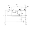
図8に従来の定電流駆動回路を示す。この回路は、LED等の負荷に定電流を供給する駆動回路である。基準電圧源V1、オペアンプからなる電圧出力型のエラーアンプA1、NMOSの出力トランジスタMN01、出力電流設定用の抵抗R1、およびESD保護用のダイオードD1,D2により定電流駆動本体回路10が構成される。P1は回路GND端子、P2はパワーGND端子であり、外部の低電圧電源端子GNDに接続される。P3は出力端子であり、この出力端子P3と外部の高電圧電源端子(VDD)との間に、定電流駆動されるLED等の負荷が接続される。端子P1〜P3は半導体集積回路に設けられる。N1は電流設定用のノードである。
FIG. 8 shows a conventional constant current drive circuit. This circuit is a drive circuit that supplies a constant current to a load such as an LED. A constant current drive
ダイオードD2は回路GND端子P1が正極となり電流設定用のノードN1が負極となるようなESD(静電気放電:Electro-Static Discharge)が印加されたときオンし、ダイオードD1はオープンした回路GND端子P1が正極となりパワーGND端子P2が負極となるようなESDが印加されたときオンし、いずれもESDから回路や素子を保護する。 The diode D2 is turned on when an ESD (Electro-Static Discharge) is applied such that the circuit GND terminal P1 is positive and the current setting node N1 is negative. The diode D1 is connected to the open circuit GND terminal P1. It is turned on when ESD is applied so that the power GND terminal P2 is a negative electrode and the power GND terminal P2 is a negative electrode, both of which protect circuits and elements from ESD.
また、基準電圧源V2、オペアンプからなる電圧出力型のエラーアンプA2、過電流検出用のNMOSトランジスタMN02、および過電流検出用の抵抗R3は、過電流保護用の保護回路40Bを構成する。
The reference voltage source V2, the voltage output type error amplifier A2 composed of an operational amplifier, the overcurrent detection NMOS transistor MN02, and the overcurrent detection resistor R3 constitute an
エラーアンプA1,A2の出力は乗算部41に入力している。この乗算部41は2個の入力電圧のうち、低い方の電圧を優先して取り出し、トランジスタMN01,MN02のゲートに入力する。
The outputs of the error amplifiers A1 and A2 are input to the
定電流駆動本体回路10では、エラーアンプA1の非反転入力端子に基準電圧源V1が接続され、エラーアンプA1により出力トランジスタMN01が駆動される。出力トランジスタMN01は、そのドレインが出力端子P3へ、ソースが電流設定用のノードN1へ接続され、出力端子P3から電流設定用のノードN1へ流れる電流を制御する。また、エラーアンプA1の反転入力端子には、出力トランジスタMN01のソース電圧、即ち電流設定用のノードN1の電圧が入力される。この結果、エラーアンプA1は出力トランジスタMN01を介して負帰還動作し、電流設定用のノードN1は基準電圧源V1と同等の電圧に制御される。
In the constant current drive
そして、電流設定用のノードN1とパワーGND端子P2との間に接続された電流設定用の抵抗R1により、出力端子P3からは、一定電流(シンク電流)が出力される。このときの出力電流IOUTは、基準電圧源V1の電圧をV1、抵抗R1の抵抗値をR1とすると、
IOUT=V1/R1 (1)
で決まる値に設定される。
A constant current (sink current) is output from the output terminal P3 by the current setting resistor R1 connected between the current setting node N1 and the power GND terminal P2. At this time, the output current IOUT is V1 as the voltage of the reference voltage source V1, and R1 as the resistance value of the resistor R1.
IOUT = V1 / R1 (1)
It is set to a value determined by.
保護回路40Bでは、トランジスタMN02がトランジスタMN01と同様にエラーアンプA1によって駆動される。トランジスタMN02には抵抗R3が接続され、そのトランジスタMN02と抵抗R3の直列回路は、出力トランジスタMN01と同様に、出力端子P3と電流設定用のノードN1との間に挿入されている。ここで、トランジスタMN02の素子サイズは、トランジスタMN01に対して極めて小さく設定される。このため、出力端子P3を流れる出力電流IOUTは、その大部分がトランジスタMN01へ流れる。
In the
しかし、トランジスタMN02はそのゲートが出力トランジスタMN01と共通に接続され、エラーアンプA1により駆動されているため、トランジスタMN02にはトランジスタMN01のドレイン電流、即ち出力電流IOUTに応じた電流が流れ、その抵抗R3の両端には出力電流IOUTに応じた電圧が発生する。 However, since the gate of the transistor MN02 is commonly connected to the output transistor MN01 and is driven by the error amplifier A1, a current corresponding to the drain current of the transistor MN01, that is, the output current IOUT flows through the transistor MN02, and its resistance A voltage corresponding to the output current IOUT is generated at both ends of R3.
そして、エラーアンプA2には、電流設定用のノードN1を基準にして、基準電圧V2と抵抗R3の両端に発生した電圧の差電圧が入力され、その出力はエラーアンプA1と同様、トランジスタMN01とトランジスタMN02のゲートへ接続される。 The error amplifier A2 receives the difference voltage between the reference voltage V2 and the voltage generated across the resistor R3 with reference to the current setting node N1, and the output is similar to that of the error amplifier A1. Connected to the gate of transistor MN02.
これにより、トランジスタMN02の電流が増加し、抵抗R3の両端電圧が基準電圧源V2の電圧を超えると、エラーアンプA2の出力電圧が低下するので、乗算部41によってそのエラーアンプA2の出力電圧が優先されて、トランジスタMN01,MN02のゲート電圧が引き下げられ、トランジスタMN01,MN02のドレイン電流、即ち出力電流IOUTが減少する。以上のような動作により、出力端子P3からの出力電流IOUTが一定値を超えないように制御される。 As a result, when the current of the transistor MN02 increases and the voltage across the resistor R3 exceeds the voltage of the reference voltage source V2, the output voltage of the error amplifier A2 decreases. As a priority, the gate voltages of the transistors MN01 and MN02 are lowered, and the drain currents of the transistors MN01 and MN02, that is, the output current IOUT decreases. By the operation as described above, the output current IOUT from the output terminal P3 is controlled so as not to exceed a certain value.
このように、出力電流IOUTが一定値まで増加した場合に保護回路40Bが働き、過電流による出力トランジスタMN01の破壊が防止される。出力電流IOUTの増加は、電流設定用の抵抗R1を推奨値外の低抵抗値に設定した場合や、電流設定用のノードN1がGNDと短絡した場合等に発生する。
As described above, when the output current IOUT increases to a certain value, the
ところで、上記した正常動作時、エラーアンプA1等の各回路の電流は、回路GND端子P1とパワーGND端子P2を介して外部のGNDへ流れる。ここで異常状態として、回路GND端子P1がGNDへ接続されずオープンとなった場合、エラーアンプA1の動作電流等の回路電流により、回路GND端子P1の電圧は上昇する。 By the way, during the normal operation described above, the current of each circuit such as the error amplifier A1 flows to the external GND via the circuit GND terminal P1 and the power GND terminal P2. Here, when the circuit GND terminal P1 is opened without being connected to GND as an abnormal state, the voltage of the circuit GND terminal P1 rises due to a circuit current such as an operating current of the error amplifier A1.
通常、半導体集積回路内で上記した定電流駆動本体回路10を構成した場合には、回路GND端子P1に対し、電流設定用のノードN1やパワーGND端子P2との間にESD保護ダイオードD1,D2が接続される。このため、回路GND端子P1がオープンになると、これらのダイオードD1,D2が順方向へオンした時点で、回路GND端子P1の電圧上昇は停止する。このとき、回路GND端子P1の電圧は、正常動作時に比べてダイオードD1,D2の順方向電圧分だけ高い電圧に保持される。なお、ESD保護ダイオードD1,D2が無い場合は更に回路GND端子P1の電圧が上昇する。
Normally, when the above-described constant current drive
以上のような異常状態は、回路GND端子P1とパワーGND端子P2が別々に設けられた場合において、回路GND端子P1の半田不良や基板パターン欠陥等によって起こり得る。なお、特許文献1には、半導体集積回路のGND端子や電源端子がオープン状態であることを検出する検出回路について明示されている。 The abnormal state as described above may occur due to a defective solder of the circuit GND terminal P1, a substrate pattern defect, or the like when the circuit GND terminal P1 and the power GND terminal P2 are provided separately. Patent Document 1 clearly discloses a detection circuit that detects that a GND terminal and a power supply terminal of a semiconductor integrated circuit are in an open state.
ここで、回路GND端子P1がオープンとなった状態での定電流駆動本体回路10の動作を考えると、エラーアンプA1の非反転入力端子へ入力される電圧は、基準電圧源V1の電圧V1に回路GND端子P1の電圧上昇分が加算された電圧となる。この結果、電流設定用のノードN1も正常動作時に比べて回路GND端子P1の電圧上昇分だけ増加した電圧となる。このため、出力電流IOUTは基準電圧V1と電流設定用の抵抗R1によって設定した値(=V1/R1)より増大する問題が生じる。
Here, considering the operation of the constant current drive
出力電流IOUTの増加量は回路GND端子P1の電圧上昇量に比例するが、前述の保護回路40Bが動作するまでの期間では出力電流IOUTが増加する恐れがある。即ち電流設定用の抵抗R1が正常動作可能な範囲の値に設定されている状態であっても、出力電流IOUTが予め設定した電流に比べ大きくなる状態となる。
The increase amount of the output current IOUT is proportional to the voltage increase amount of the circuit GND terminal P1, but the output current IOUT may increase during the period until the
本発明の目的は、回路GND端子等の端子がオープンとなる状態において出力トランジスタの過電流を防止する過電流保護回路を最小限の回路追加で構成することである。 An object of the present invention is to configure an overcurrent protection circuit that prevents an overcurrent of an output transistor in a state in which a terminal such as a circuit GND terminal is open with a minimum circuit addition.
上記目的を達成するために、請求項1にかかる発明は、第1の電源端子に接続される第1の端子と、前記第1の電源端子に接続される第2の端子と、前記第2の端子と第1のノードとの間に接続された電流設定用の第1の抵抗と、第2の電源端子との間に負荷が接続される出力端子と、該出力端子と前記第1のノードとの間に接続された出力トランジスタと、前記第1のノードの電圧が前記第1の端子を基準端子とする電圧源で設定される基準電圧と等しくなるように前記出力トランジスタを制御する第1のエラーアンプと、を備える定電流駆動本体回路を有し、前記第1の端子と前記第2の端子との間に第1のESD保護素子が接続されるようにした定電流駆動回路において、前記第1の端子の電圧と前記第2の端子の電圧に所定の差分が生じたとき前記出力トランジスタの出力電流が減少するように前記出力トランジスタを制御する過電流保護回路を設けたことを特徴とする。 In order to achieve the above object, the invention according to claim 1 includes a first terminal connected to a first power supply terminal, a second terminal connected to the first power supply terminal, and the second terminal. A first resistor for current setting connected between the first terminal and the first node, an output terminal connected to a load between the second power supply terminal, the output terminal and the first node And an output transistor connected between the first node and the first transistor for controlling the output transistor so that a voltage at the first node is equal to a reference voltage set by a voltage source having the first terminal as a reference terminal. A constant current drive main circuit having a first error amplifier, wherein a first ESD protection element is connected between the first terminal and the second terminal. , There is a predetermined difference between the voltage at the first terminal and the voltage at the second terminal. Wherein the output current of the output transistor when the Flip is provided an overcurrent protection circuit for controlling the output transistor so as to reduce.
請求項2にかかる発明は、第1の電源端子に接続される第1の端子と、前記第1の電源端子と第1のノードとの間に接続された電流設定用の第1の抵抗と、第2の電源端子との間に負荷が接続される出力端子と、該出力端子と前記第1のノードとの間に接続された出力トランジスタと、前記第1のノードの電圧が前記第1の端子を基準端子とする電圧源で設定される基準電圧と等しくなるように前記出力トランジスタを制御する第1のエラーアンプと、を備える定電流駆動本体回路を有し、前記第1の端子と前記第1のノードとの間に第2のESD保護素子が接続されるようにした定電流駆動回路において、前記第1の端子の電圧と前記第1のノードの電圧に所定の差分が生じたとき前記出力トランジスタの出力電流が減少するように前記出力トランジスタを制御する過電流保護回路を設けたことを特徴とする。 According to a second aspect of the present invention, a first terminal connected to the first power supply terminal, a first resistor for current setting connected between the first power supply terminal and the first node, , An output terminal connected to a load between the second power supply terminal, an output transistor connected between the output terminal and the first node, and a voltage at the first node being the first A constant current drive main body circuit comprising: a first error amplifier that controls the output transistor so as to be equal to a reference voltage set by a voltage source having a terminal as a reference terminal; and In a constant current drive circuit in which a second ESD protection element is connected between the first node and the first node, a predetermined difference occurs between the voltage at the first terminal and the voltage at the first node. When the output transistor so that the output current of the output transistor decreases. Characterized by providing an overcurrent protection circuit for controlling the transistors.
請求項3にかかる発明は、請求項1又は2に記載の定電流駆動回路において、前記過電流保護回路は、前記第1の端子が前記第1の電源端子からオープン状態になったとき該オープン状態を示す検出信号を出力する端子オープン検出回路と、該端子オープン検出回路が前記検出信号を出力するときに前記出力トランジスタの出力電流を低減する保護回路と、からなることを特徴とする。 According to a third aspect of the present invention, in the constant current drive circuit according to the first or second aspect, the overcurrent protection circuit is configured to open the first terminal when the first terminal is opened from the first power supply terminal. A terminal open detection circuit that outputs a detection signal indicating a state, and a protection circuit that reduces an output current of the output transistor when the terminal open detection circuit outputs the detection signal.
請求項4にかかる発明は、請求項1に記載の定電流駆動回路において、前記過電流保護回路は、前記第1の端子が前記第1の電源端子からオープン状態になったとき該オープン状態を示す検出信号を出力する端子オープン検出回路と、該端子オープン検出回路が前記検出信号を出力するときに前記出力トランジスタの出力電流を低減する保護回路とからなり、前記端子オープン検出回路は、前記第1の端子の電圧を検出する第1のトランジスタと、前記第2の端子の電圧を検出する第2のトランジスタとを備え、前記第1の端子の電圧と前記第2の端子の電圧に所定の差分が生じているとき前記検出信号を出力することを特徴とする。
Such invention in claim 4, the constant current driving circuit according to claim 1, wherein the overcurrent protection circuit, the open state when the first terminal is in an open state from the first power supply terminal A terminal open detection circuit that outputs a detection signal, and a protection circuit that reduces an output current of the output transistor when the terminal open detection circuit outputs the detection signal . A first transistor for detecting a voltage at one terminal and a second transistor for detecting a voltage at the second terminal, wherein the voltage at the first terminal and the voltage at the second terminal are predetermined. The detection signal is output when a difference occurs.
請求項5にかかる発明は、請求項3に記載の定電流駆動回路において、前記端子オープン検出回路は、前記第1の端子の電圧を検出する第1のトランジスタと、前記第1のノードの電圧を検出する第2のトランジスタとを備え、前記第1の端子の電圧と前記第1のノードの電圧に所定の差分が生じているとき前記検出信号を出力することを特徴とする。 According to a fifth aspect of the present invention, in the constant current drive circuit according to the third aspect, the terminal open detection circuit includes a first transistor that detects a voltage of the first terminal, and a voltage of the first node. And detecting a signal when a predetermined difference occurs between the voltage at the first terminal and the voltage at the first node.
請求項6にかかる発明は、請求項3、4又は5に記載の定電流駆動回路において、前記保護回路は、前記第1のノードと前記第1のエラーアンプの一方の入力端子との間に接続され、且つ前記端子オープン検出回路が前記検出信号を出力することにより電圧が発生する第2の抵抗からなり、該第2の抵抗に発生する該電圧により前記第1のエラーアンプが前記出力トランジスタを前記出力電流を低減するよう制御することを特徴とする。 The invention according to claim 6 is the constant current drive circuit according to claim 3, 4 or 5, wherein the protection circuit is provided between the first node and one input terminal of the first error amplifier. A second resistor that generates a voltage when the terminal open detection circuit outputs the detection signal, and the first error amplifier is connected to the output transistor by the voltage generated in the second resistor. Is controlled to reduce the output current.
請求項7にかかる発明は、請求項3、4又は5に記載の定電流駆動回路において、前記保護回路は、前記出力トランジスタとゲートおよびドレインが共通接続された保護用トランジスタと、該保護用トランジスタのソースと前記第1のノードとの間に接続された第3の抵抗と、前記第3の抵抗に生ずる電圧が所定の電圧となるように前記出力トランジスタおよび前記保護用トランジスタのゲートを制御する第2のエラーアンプとを備え、前記端子オープン検出回路が前記検出信号を出力することにより、前記第2のエラーアンプが前記出力トランジスタの前記出力電流および前記保護用トランジスタに流れる電流を減少させることを特徴とする。 The invention according to claim 7 is the constant current drive circuit according to claim 3, 4 or 5, wherein the protection circuit includes a protection transistor having a gate and a drain connected in common to the output transistor, and the protection transistor. And a gate of the output transistor and the protection transistor so that a voltage generated in the third resistor is a predetermined voltage. The third resistor is connected between the source of the transistor and the first node. A second error amplifier, and the terminal open detection circuit outputs the detection signal, so that the second error amplifier reduces the output current of the output transistor and the current flowing through the protection transistor. It is characterized by.
請求項8にかかる発明は、請求項3、4又は5に記載の定電流駆動回路において、前記保護回路は、前記出力トランジスタのゲート・ソース間に接続され、且つ前記端子オープン検出回路が前記検出信号を出力することにより導通する第3のトランジスタからなることを特徴とする。 The invention according to claim 8 is the constant current drive circuit according to claim 3, 4 or 5, wherein the protection circuit is connected between a gate and a source of the output transistor, and the terminal open detection circuit is the detection It is characterized by comprising a third transistor which is turned on by outputting a signal.
請求項9にかかる発明は、請求項3乃至8のいずれか1つに記載の定電流駆動回路において、前記出力端子の電圧が所定値を超えたとき検出信号を出力する電圧監視回路を備え、該電圧監視回路が前記検出信号を出力すると、前記端子オープン検出回路が前記出力信号を出すことを特徴とする。
The invention according to
本発明によれば、第1の端子が第1の電源端子に接続されないオープン状態になったとき、出力トランジスタへ過電流が流れることを防止することを、最小限の回路追加で実現することができる。 According to the present invention, it is possible to prevent the overcurrent from flowing to the output transistor when the first terminal is not connected to the first power supply terminal, with minimal circuit addition. it can.
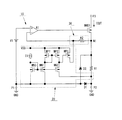
<第1の実施例>
図1に本発明の第1の実施例の定電流駆動回路を示す。本実施の定電流駆動回路は、定電流駆動本体回路10と端子オープン検出回路20と保護回路30とで構成される。定電流駆動本体回路10は、エラーアンプA1、出力トランジスタMN01、基準電圧源V1、電流設定用の抵抗R1、ESD保護ダイオードD1,D2、回路GND端子P1、パワーGND端子P2、出力端子P3を備える。端子オープン検出回路20は、基準電流源I1、NMOSトランジスタMN1〜MN3、PMOSトランジスタMP1〜MP3を備える。保護回路30は抵抗R2で構成される。
<First embodiment>
FIG. 1 shows a constant current drive circuit according to a first embodiment of the present invention. The constant current drive circuit according to the present embodiment includes a constant current drive
端子オープン検出回路20において、トランジスタMN1〜MN3は電流源I1の電流を折り返すカレントミラーを構成し、トランジスタMP1,MP2はトランジスタMN1のドレイン電流を折り返すカレントミラーを構成する。
In the terminal
トランジスタMN1,MN2,MN3の素子サイズは同じに設定されている。トランジスタMP1,MP2の素子サイズは、トランジスタMP2がトランジスタMP1に対して大きくなるように、例えば1:2に設定されている。トランジスタMP3は、トランジスタMP2とMN2のドレイン電流の差分が所定値になることによりゲート電圧が低下して、ドレイン電流を検出信号として出力する。 The element sizes of the transistors MN1, MN2, and MN3 are set to be the same. The element sizes of the transistors MP1 and MP2 are set to, for example, 1: 2 so that the transistor MP2 is larger than the transistor MP1. The transistor MP3 outputs the drain current as a detection signal because the gate voltage is lowered when the difference between the drain currents of the transistors MP2 and MN2 becomes a predetermined value.
ここでは、請求項に記載の「第1のトランジスタ」はトランジスタMN1、MN3,MP1,MP2で構成され、「第2のトランジスタ」はトランジスタMN2で構成されている。 Here, the “first transistor” recited in the claims includes transistors MN1, MN3, MP1, and MP2, and the “second transistor” includes transistor MN2.
保護回路30としての抵抗R2は、電流設定用のノードN1とエラーアンプA1の反転入力端子との間に接続され、端子オープン検出回路20からの検出信号がそこに流れると電圧が発生し、エラーアンプA1の反転入力端子の電圧を上昇させる。
The resistor R2 as the
さて、回路GND端子P1がGNDに正常に接続されている状態では、トランジスタMN1,MN2,MN3のドレイン電流は電流源I1の電流I1となる。トランジスタMP1のドレイン電流はI1であるがトランジスタMP2のドレイン電流は2I1となる。よって、トランジスタMP2とMN2の共通ドレイン電圧は、中点電圧であるVDD/2よりも大幅に高くなり、トランジスタMP3はそのゲート電圧が高くなってオフしている。 When the circuit GND terminal P1 is normally connected to GND, the drain currents of the transistors MN1, MN2, and MN3 are the current I1 of the current source I1. The drain current of the transistor MP1 is I1, but the drain current of the transistor MP2 is 2I1. Therefore, the common drain voltage of the transistors MP2 and MN2 is significantly higher than VDD / 2 which is the midpoint voltage, and the transistor MP3 is turned off due to its gate voltage becoming high.
このため、トランジスタMP3にドレイン電流は流れず、即ち検出電流は発生せず、電流設定用のノードN1の電圧がそのままエラーアンプA1の反転入力端子に入力し、出力トランジスタMN01は出力電流IOUTが前記した式(1)で示される定電流となるように、制御される。 Therefore, no drain current flows through the transistor MP3, that is, no detection current is generated, the voltage of the current setting node N1 is directly input to the inverting input terminal of the error amplifier A1, and the output transistor MN01 outputs the output current IOUT. Control is performed so as to obtain a constant current represented by the equation (1).
一方、回路GND端子P1がオープンとなりその端子P1の電圧が上昇した場合、図8の従来回路で説明したのと同様に、エラーアンプA1の非反転入力端子の電圧が基準電圧源V1の電圧V1よりもESD保護ダイオードD1,D2の順方向電圧分だけ上昇し、これによって出力トランジスタMN01の出力電流IOUTが増大する。 On the other hand, when the circuit GND terminal P1 is opened and the voltage at the terminal P1 rises, the voltage at the non-inverting input terminal of the error amplifier A1 is the voltage V1 of the reference voltage source V1 as described in the conventional circuit of FIG. More than the forward voltage of the ESD protection diodes D1 and D2, thereby increasing the output current IOUT of the output transistor MN01.
しかし、この回路GND端子P1のオープン状態は、以下に述べるように、端子オープン検出回路20によって検出され、出力トランジスタMN01の電流IOUTの増大が抑制される。
However, the open state of the circuit GND terminal P1 is detected by the terminal
端子オープン検出回路20において、トランジスタMN1,MN3のゲートおよびソースの電圧は、回路GND端子P1の電圧上昇と共に上昇するが、トランジスタMN1,MN3へ流れる電流は基準電流源I1により制限されているため電流I1からの変化は無い。また、トランジスタMN1のドレイン電流により駆動されているトランジスタMP1,MP2の電流にも、変化は無い。
In the terminal
ところが、トランジスタMN2は、そのソース電圧がパワーGND端子P2を通じてGND電位を保持しているのに対し、ゲート電圧が回路GND端子P1の電位上昇と共に上昇するので、ゲート・ソース間電圧が大きくなってドレイン電流が増加する。このため、トランジスタMP2,MN2の共通ドレイン電圧、即ちトランジスタMP3のゲート電圧が引き下げられ、そのトランジスタMP3にドレイン電流が流れる。このようにして、回路GND端子P1がオープンしていることを示す検出信号(ドレイン電流)が出力する。 However, since the source voltage of the transistor MN2 holds the GND potential through the power GND terminal P2, the gate voltage increases as the potential of the circuit GND terminal P1 rises, so that the gate-source voltage increases. The drain current increases. For this reason, the common drain voltage of the transistors MP2 and MN2, that is, the gate voltage of the transistor MP3 is lowered, and a drain current flows through the transistor MP3. In this way, a detection signal (drain current) indicating that the circuit GND terminal P1 is open is output.
そして、トランジスタMP3のドレイン電流は、抵抗R2および電流設定用の抵抗R1を流れ、さらにパワーGND端子P2を通じてGNDへ流れる。このため、エラーアンプA1の反転入力端子電圧が上昇する。 The drain current of the transistor MP3 flows through the resistor R2 and the current setting resistor R1, and further flows to GND through the power GND terminal P2. For this reason, the inverting input terminal voltage of the error amplifier A1 increases.
この結果、エラーアンプA1の出力電圧、即ち出力トランジスタMN01のゲート電圧が引き下げられ、MOSトランジスタMN01は、そのドレイン電流である出力電流IOUTの増加を抑制する。 As a result, the output voltage of the error amplifier A1, that is, the gate voltage of the output transistor MN01 is lowered, and the MOS transistor MN01 suppresses an increase in the output current IOUT that is the drain current.
なお、上記実施例では、トランジスタMP1,MP2の素子サイズを1:2に設定することで正常動作時にトランジスタMP3がオフになるようにしたが、これに限られるものではない。例えば、トランジスタMP1,MP2の素子サイズは1:1に設定し、トランジスタMN1,MN3の素子サイズも1:1に設定する。そして、トランジスタMN3,MN2の素子サイズを2:1に設定する。これによっても、正常動作時にトランジスタMP2,MN2の共通ドレイン電圧を高くしてトランジスタMP3をオフに制御し、回路GND端子P1がオープンになったときにトランジスタMP3を導通させて、トランジスタMP3に検出電流が流れるようにすることができる。 In the above embodiment, the element size of the transistors MP1 and MP2 is set to 1: 2 so that the transistor MP3 is turned off during normal operation. However, the present invention is not limited to this. For example, the element sizes of the transistors MP1 and MP2 are set to 1: 1, and the element sizes of the transistors MN1 and MN3 are also set to 1: 1. Then, the element sizes of the transistors MN3 and MN2 are set to 2: 1. This also increases the common drain voltage of the transistors MP2 and MN2 during normal operation to control the transistor MP3 to turn off, and causes the transistor MP3 to conduct when the circuit GND terminal P1 is opened, causing the transistor MP3 to detect current. Can flow.
以上から第1の実施例の定電流駆動回路によれば、回路GND端子P1のオープン時に出力トランジスタMN01の出力電流IOUTが過電流になることを防止することができる。 As described above, according to the constant current drive circuit of the first embodiment, it is possible to prevent the output current IOUT of the output transistor MN01 from becoming an overcurrent when the circuit GND terminal P1 is opened.
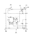
<第2の実施例>
図2に本発明の第2の実施例の定電流駆動回路を示す。定電流駆動本体回路10と端子オープン検出回路20は、前述の第1の実施例の定電流駆動回路と同じである。本実施例は、保護回路30に代えて保護回路40を新たに構成している。この保護回路40は、図8の従来回路で説明した保護回路40Bと類似であるが、トランジスタMN02と抵抗R3の共通接続点とエラーアンプA2の反転入力端子との間に新たに抵抗R4を接続し、その反転入力端子に端子オープン検出回路20のトランジスタMP3のドレインを接続して構成している点が異なっている。
<Second embodiment>
FIG. 2 shows a constant current drive circuit according to a second embodiment of the present invention. The constant current drive
さて、回路GND端子P1がGNDに正常に接続されているときは、端子オープン検出回路20のトランジスタMP3からドレイン電流は流れず、電流設定用のノードN1の電圧がそのままエラーアンプA1の反転入力端子に入力する。このため、出力トランジスタMN01は出力電流IOUTが前記した式(1)で示される定電流となるように、制御される。
When the circuit GND terminal P1 is normally connected to GND, the drain current does not flow from the transistor MP3 of the terminal
また、保護回路40では、図8の従来回路で説明した保護回路40Bと同様に、出力電流IOUTが増大したときに、抵抗R3に流れる電流が増大してトランジスタMN02のソース電圧が上昇し、その電圧が抵抗R4を経由してエラーアンプA2の反転入力端子に印加するので、その反転入力端子の電圧を上昇させる。これにより、出力トランジスタMN01のゲート電圧が低下し、その出力電流IOUTが減少する。
Further, in the
一方、回路GND端子P1がオープンとなり端子P1の電圧が上昇した場合は、第1の実施例で説明したのと同様に、エラーアンプA1の非反転入力端子の電圧が電圧源V1の電圧よりもESD保護ダイオードD1,D2の順方向電圧分だけ上昇し、これによって出力トランジスタMN01の出力電流IOUTが増大する。 On the other hand, when the circuit GND terminal P1 is opened and the voltage at the terminal P1 rises, the voltage at the non-inverting input terminal of the error amplifier A1 is higher than the voltage at the voltage source V1 as described in the first embodiment. The voltage increases by the forward voltage of the ESD protection diodes D1 and D2, thereby increasing the output current IOUT of the output transistor MN01.
しかし、この回路GND端子P1のオープンは、以下に述べるように、端子オープン検出回路20によって検出され、その検出結果に応じて保護回路40により、出力トランジスタMN01の電流IOUTの増大が抑制される。
However, the opening of the circuit GND terminal P1 is detected by the terminal
即ち端子オープン検出回路20によって端子P1のオープンが検出されると、端子オープン検出回路20のトランジスタMP3にドレイン電流が流れ、この電流が抵抗R4,R3、R1を経由してパワーGND端子P2からGNDに流れるので、エラーアンプA2の反転入力端子の電圧が上昇し、そのエラーアンプA2の出力電圧が低下する。これによって、トランジスタMN01,MN02のゲート電圧が低下し、出力電流IOUTの増大が抑制される。
That is, when the terminal
本実施例の定電流駆動回路によれば、回路GND端子P1オープン時の端子P1の電圧上昇を検出し、出力トランジスタMN01に過電流が流れることを防止し、損失増加による破壊等を回避することができ、第1の実施例の定電流駆動回路と同様の効果が得られる。 According to the constant current drive circuit of the present embodiment, a voltage rise at the terminal P1 when the circuit GND terminal P1 is open is detected, an overcurrent is prevented from flowing through the output transistor MN01, and destruction due to an increase in loss is avoided. The same effect as the constant current drive circuit of the first embodiment can be obtained.
ところで、第1の実施例の定電流駆動回路では、端子オープン検出回路20の出力をエラーアンプA1の反転入力端子へ直接接続していたため、正常動作時の定電流駆動本体回路10の出力電流設定値へ悪影響を及ぼす恐れがあった。そこで、上述のようにトランジスタMP1,2の素子サイズ比あるいはトランジスタMN2,MN3の素子サイズ比を適宜設定することで、正常動作時に定電流駆動本体回路10に与える影響を低減していた。
By the way, in the constant current drive circuit of the first embodiment, since the output of the terminal
しかし、端子オープン検出回路20のトランジスタMP3のオフ時リーク電流が増加した場合には、この問題に対処できない。
However, this problem cannot be addressed when the off-state leakage current of the transistor MP3 of the terminal
そこで第2の実施例の定電流駆動回路では、端子オープン検出回路20の出力を正常動作に影響を与えないエラーアンプA2の反転入力端子へ接続する構成としている。これによれば、トランジスタMP3のオフ時リーク電流が増加した場合、保護回路40の動作に影響を与える恐れはあるものの、より高精度が求められる正常動作時の定電流駆動本体回路10の出力電流IOUTの設定精度への影響は無くなる。
Therefore, in the constant current drive circuit of the second embodiment, the output of the terminal
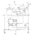
<第3の実施例>
図3に本発明の第3の実施例の定電流駆動回路を示す。10Aは定電流駆動本体回路であり、第1および第2の実施例の定電流駆動本体回路10とは、定電流制御用のエラーアンプとして、電流出力型(Gmアンプ形式)のエラーアンプA3を使用している点が異なっている。20Aは端子オープン検出回路であり、第1および第2の実施例で説明した端子オープン検出回路20とは、トランジスタMP2,MN2の共通ドレインから検出信号を取り出す点と、トランジスタMN1のソースをパワーGND端子P2に接続した点が異なっている。
<Third embodiment>
FIG. 3 shows a constant current drive circuit according to a third embodiment of the present invention.
なお、トランジスタMN1,MN3は同じ素子サイズ、トランジスタMP1,MP2も同じ素子サイズであるが、トランジスタMN1,MN2の素子サイズは、1:2である。ここでは、請求項に記載の「第1のトランジスタ」はトランジスタMN2、MN3で構成され、「第2のトランジスタ」はトランジスタMN1,MP1,MP2で構成されている。 The transistors MN1 and MN3 have the same element size, and the transistors MP1 and MP2 have the same element size. However, the element sizes of the transistors MN1 and MN2 are 1: 2. Here, the “first transistor” recited in the claims includes transistors MN2 and MN3, and the “second transistor” includes transistors MN1, MP1, and MP2.
50は端子オープン検出回路20の出力で制御されるトランジスタMN4からなる保護回路であり、出力トランジスタMN01のゲート・ソース間に接続されている。このトランジスタMN4は請求項に記載の「第3のトランジスタ」を構成する。
50 is a protection circuit comprising a transistor MN4 controlled by the output of the terminal
さて、回路GND端子P1がGNDに正常に接続されているときは、端子オープン検出回路20Aでは、トランジスタMP2に電流I1が流れ、トランジスタMN2にその2倍の電流2I1が流れるので、トランジスタMP2,MN2の共通ドレインの電圧が低下し、保護回路50のトランジスタMN4はオフしている。このため、出力トランジスタMN01は出力電流IOUTが前記した式(1)で示される定電流となるように、制御される。
When the circuit GND terminal P1 is normally connected to GND, in the terminal
一方、回路GND端子P1がオープンとなり端子P1の電圧が上昇した場合は、第1の実施例で説明したのと同様に、エラーアンプA3の非反転入力端子の電圧が基準電圧源V1の電圧V1よりもESD保護ダイオードD1,D2の順方向電圧分だけ上昇し、これによって出力トランジスタMN01の出力電流IOUTが増大する。 On the other hand, when the circuit GND terminal P1 is opened and the voltage at the terminal P1 rises, the voltage at the non-inverting input terminal of the error amplifier A3 is equal to the voltage V1 of the reference voltage source V1 as described in the first embodiment. More than the forward voltage of the ESD protection diodes D1 and D2, thereby increasing the output current IOUT of the output transistor MN01.
しかし、この回路GND端子P1のオープンは、以下に述べるように、端子オープン検出回路20Aによって検出され、その検出結果に応じて保護回路50により、出力トランジスタMN01のゲート・ソース間が短絡され出力電流IOUTが遮断される。
However, the opening of the circuit GND terminal P1 is detected by the terminal
回路GND端子P1がオープンになると、トランジスタMN1〜MN3のゲート電位が上昇する。このとき、トランジスタMN2,MN3の動作は正常動作時から変化しない。一方、トランジスタMN1は、そのソース電位がパワーGND端子P2を介してGND電位に固定されているため、ゲート・ソース間電圧が増大し、ドレイン電流が増加する。これにより、トランジスタMP1,MP2のドレイン電流も増加し、トランジスタMP2のドレイン電流がトランジスタMN2のドレイン電流を上回ると、トランジスタMN4はそのゲート電圧が上昇するためオン状態となる。この結果、出力トランジスタMN01のゲート・ソース間電圧がほぼ0Vとなり、出力トランジスタMN01はオフする。 When the circuit GND terminal P1 is opened, the gate potentials of the transistors MN1 to MN3 rise. At this time, the operation of the transistors MN2 and MN3 does not change from the normal operation. On the other hand, since the source potential of the transistor MN1 is fixed to the GND potential via the power GND terminal P2, the gate-source voltage increases and the drain current increases. As a result, the drain currents of the transistors MP1 and MP2 also increase, and when the drain current of the transistor MP2 exceeds the drain current of the transistor MN2, the transistor MN4 is turned on because its gate voltage increases. As a result, the gate-source voltage of the output transistor MN01 becomes almost 0 V, and the output transistor MN01 is turned off.
このとき、エラーアンプA3としてGmアンプを使用しているので、トランジスタMN4がオンとなっても、エラーアンプA3からそのトランジスタMN4に流れる電流が規制される。このエラーアンプA3を使用せず、第1および第2の実施例のような電圧出力型のエラーアンプA1を使用する場合は、トランジスタMN4に過大な電流が流れるが、これを防止できる。ただし、電圧出力型のエラーアンプA1の出力インピーダンスを大きくした場合には、トランジスタMN4に流れる電流を規制できるので、そのエラーアンプA1をそのまま使用することができる。 At this time, since the Gm amplifier is used as the error amplifier A3, even if the transistor MN4 is turned on, the current flowing from the error amplifier A3 to the transistor MN4 is regulated. When the voltage output type error amplifier A1 as in the first and second embodiments is used without using the error amplifier A3, an excessive current flows through the transistor MN4, which can be prevented. However, when the output impedance of the voltage output type error amplifier A1 is increased, the current flowing through the transistor MN4 can be regulated, so that the error amplifier A1 can be used as it is.
ここで、第1および第2の実施例の定電流駆動回路では、GND端子P1オープン時の出力トランジスタMN01のゲート電圧をエラーアンプA1やエラーアンプA2が出力しており、回路構成上、各エラーアンプA1,A2の出力電圧は電圧上昇した回路GND端子P1の電位より低い電圧にはならない。よって、第1および第2の実施例では、出力トランジスタMN01のゲート・ソース間電圧を0Vにすることができない動作条件が存在する。例えば、第1および第2の実施例において、回路GND端子P1の電位上昇の検出条件(オープンの検出条件)を1V上昇時とした場合、出力トランジスタMN01のゲート電圧を1V以下に下げることはできない。 Here, in the constant current drive circuits of the first and second embodiments, the error amplifier A1 and the error amplifier A2 output the gate voltage of the output transistor MN01 when the GND terminal P1 is open. The output voltages of the amplifiers A1 and A2 do not become lower than the potential of the circuit GND terminal P1 whose voltage has increased. Therefore, in the first and second embodiments, there is an operating condition in which the gate-source voltage of the output transistor MN01 cannot be 0V. For example, in the first and second embodiments, the gate voltage of the output transistor MN01 cannot be lowered to 1 V or lower when the detection condition (open detection condition) of the potential rise of the circuit GND terminal P1 is 1 V. .
これに対し第3の実施例の定電流駆動回路は、トランジスタMN4によって出力トランジスタMN01のゲート・ソース間電圧を0Vにすることが可能であるので、回路GND端子P1の電位上昇時に出力トランジスタMN01を確実にオフ状態とすることができる。 On the other hand, in the constant current drive circuit of the third embodiment, the gate-source voltage of the output transistor MN01 can be set to 0 V by the transistor MN4, so that the output transistor MN01 is turned on when the potential at the circuit GND terminal P1 rises. It can be surely turned off.
以上のように第3の実施例の定電流駆動回路では、回路GND端子P1がオープンとなるような異常状態発生時に出力トランジスタMN01をオフにし、出力電流IOUTをゼロにすることができる。また、端子オープン検出回路20Aの検出電圧そのものに依らず、出力トランジスタMN01をオフにすることが可能となるため、出力トランジスタMN01をより広いGND電位検出条件で保護することができる。
As described above, in the constant current drive circuit of the third embodiment, the output transistor MN01 can be turned off and the output current IOUT can be made zero when an abnormal state occurs in which the circuit GND terminal P1 is open. Further, since the output transistor MN01 can be turned off regardless of the detection voltage itself of the terminal
なお、回路GND端子P1のオープン等異常状態発生時においては、出力トランジスタMN01に過電流が流れることを防止することを目的として、その出力電流IOUTをゼロにすることが回路構成上理想であるが、出力電流IOUTをゼロにすることが最善ではないアプリケーションも存在する。 When an abnormal state such as an open circuit GND terminal P1 occurs, the output current IOUT is ideally set to zero for the purpose of preventing an overcurrent from flowing through the output transistor MN01. There are also applications where it is not best to zero the output current IOUT.
例えば、定電流駆動回路の負荷としてLEDを接続し、その光源を車載ヘッドライトや非常時誘導灯として使用した場合、回路上異常状態が発生しても負荷LEDに電流を流し続け、光源としての役割を維持することが求められる。このような場合、異常状態発生時に出力電流IOUTをゼロにするのではなく、第3の実施例と異なって、回路が故障しない範囲で電流を出力し続ける動作の方が好適である。 For example, when an LED is connected as a load of a constant current drive circuit and the light source is used as an in-vehicle headlight or emergency guide light, even if an abnormal condition occurs on the circuit, the current continues to flow through the load LED, It is required to maintain the role. In such a case, the output current IOUT is not set to zero when an abnormal condition occurs, but unlike the third embodiment, an operation of continuing to output current within a range in which the circuit does not fail is preferable.
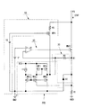
<第4の実施例>
図4に第4の実施例の定電流駆動回路を示す。20Bは端子オープン検出回路であり、トランジスタMN1のソースが電流設定ノードN1に接続されている点が、図3の第3の実施例の端子オープン検出回路20Aと異なる。ここでは、請求項に記載の「第1のトランジスタ」はトランジスタMN2,MN3で構成され、「第2のトランジスタ」はトランジスタMN1,MP1,MP2で構成されている。
<Fourth embodiment>
FIG. 4 shows a constant current driving circuit of the fourth embodiment. 20B is a terminal open detection circuit, which is different from the terminal
40Aは保護回路であり、エラーアンプA4として電流出力型(Gmアンプ形式)を使用した点と、そのエラーアンプA4の反転入力端子をトランジスタMN02のソースに直接接続した点が、第2の実施例の過電流保護回路40と異なる。
また、本実施例では、第3の実施例と同様に、出力トランジスタMN01のゲート・ソース間にトランジスタMN4からなる保護回路50を接続しているため、そのトランジスタMN4がオンする時の電流を規制するために、エラーアンプA3,A4に電流出力型を使用している。
In the present embodiment, as in the third embodiment, the
本実施例では、端子オープン検出回路20BのトランジスタMN1のソースを電流設定ノードN1に接続しているので、出力トランジスタMN01、電流設定用の抵抗R1、パワーGND端子等が半導体集積回路に外付けされる場合にも適用できる。
In the present embodiment, since the source of the transistor MN1 of the terminal
さて、回路GND端子P1がGNDに正常に接続されているときは、端子オープン検出回路20Bでは、トランジスタMN2,MN3のソース電圧はGNDであるので、それらのドレインは電流I1を引き込むが、トランジスタMN1はソース電圧はV1と高くなるのでオフする。このため、トランジスタMP1,MP2がオフして、トランジスタMP2,MN2の共通ドレインの電圧は低下している。よって、トランジスタMN4はオフしている。このため、出力トランジスタMN01は出力電流IOUTが前記した式(1)で示される定電流となるように、制御される。また、過電流が発生したときは、それが抵抗R3により検出されてエラーアンプA4の出力電流が低下し、トランジスタMN01のゲート電圧を低下させて、出力電流IOUTの増大を規制する。
Now, when the circuit GND terminal P1 is normally connected to GND, in the terminal
一方、回路GND端子P1がオープンとなり端子P1の電圧が上昇した場合は、第3の実施例で説明したのと同様に、エラーアンプA3の非反転入力端子の電圧が基準電圧源V1の電圧V1よりもESD保護ダイオードD2の順方向電圧分だけ上昇し、これによって出力トランジスタMN01の出力電流IOUTが増大する。 On the other hand, when the circuit GND terminal P1 is opened and the voltage at the terminal P1 rises, the voltage at the non-inverting input terminal of the error amplifier A3 is equal to the voltage V1 of the reference voltage source V1 as described in the third embodiment. More than the forward voltage of the ESD protection diode D2, thereby increasing the output current IOUT of the output transistor MN01.
しかし、この回路GND端子P1のオープンは、以下に述べるように、端子オープン検出回路20Bによって検出され、その検出結果に応じて保護回路50により、出力トランジスタMN01のゲート・ソース間が短絡され出力電流IOUTが遮断される。また、保護回路40Aによっても、出力電流IOUTの増大が規制される。
However, the opening of the circuit GND terminal P1 is detected by the terminal
まず、回路GND端子P1がオープンとなり、エラーアンプA3の非反転入力端子の電圧が上昇すると、電流設定ノードN1の電圧を引き上げる方向へ負帰還動作が働く。このため、出力トランジスタMN01のドレイン電流が増加するため、保護回路40Aによる過電流保護がかかり、出力トランジスタMN01のドレイン電流は減少する。すると、電流設定ノードN1の電圧も同様に低下するため、端子オープン検出回路20BのトランジスタMN1のソース電位も低下する。
First, when the circuit GND terminal P1 is opened and the voltage at the non-inverting input terminal of the error amplifier A3 is increased, a negative feedback operation is performed in the direction of increasing the voltage at the current setting node N1. For this reason, since the drain current of the output transistor MN01 increases, the overcurrent protection is applied by the
そして、電流設定ノードN1の電圧低下によりトランジスタMN1はそのゲート・ソース間電圧が上昇し、ドレイン電流が増加する。同時にカレントミラーを構成しているトランジスタMP1,MP2のドレイン電流が増加し、トランジスタMP2のドレイン電流がトランジスタMN2のドレイン電流を上回ると、トランジスタMN4はそのゲート電圧が上昇するためオン状態となる。これにより、出力トランジスタMN01のゲート・ソース間電圧が減少し、出力電流は更に低減又はゼロとなる。 Then, due to the voltage drop at the current setting node N1, the gate-source voltage of the transistor MN1 rises and the drain current increases. At the same time, when the drain currents of the transistors MP1 and MP2 constituting the current mirror increase and the drain current of the transistor MP2 exceeds the drain current of the transistor MN2, the transistor MN4 is turned on because its gate voltage increases. As a result, the gate-source voltage of the output transistor MN01 decreases, and the output current further decreases or becomes zero.
また、回路GND端子P1の電位が上昇したとき、出力トランジスタMN01のドレイン電流、即ち出力電流IOUTが増加すると、出力端子P3に接続された負荷(抵抗やLED等)の電圧降下により、出力端子P3の端子電圧が低下する。出力端子P3の電圧低下は、出力トランジスタMN01のドレイン・ソース間電圧低下となるため、出力トランジスタMN01の電流駆動能力が低下し、出力電流IOUTの減少と共に電流設定ノードN1の電圧が低下する。 Further, when the potential of the circuit GND terminal P1 rises, when the drain current of the output transistor MN01, that is, the output current IOUT increases, the voltage drop of the load (resistor, LED, etc.) connected to the output terminal P3 causes the output terminal P3. The terminal voltage decreases. Since the voltage drop at the output terminal P3 results in a voltage drop between the drain and source of the output transistor MN01, the current drive capability of the output transistor MN01 decreases, and the voltage at the current setting node N1 decreases as the output current IOUT decreases.
このように、保護回路40Aが無い場合においても、電流設定ノードN1の電圧が相対的に低下し、端子オープン検出回路20Bが回路GND端子P1のオープンを検出する。
Thus, even in the absence of the
また前述のように、端子オープン検出回路20Bの検出動作により出力電流IOUTが低減されると、電流設定ノードN1の電位も同様に低下する。このとき、トランジスタMN1は、回路GND端子P1のオープンによる端子P1の電位上昇と共にそのゲート電位が上昇し、電流設定ノードN1の電位低下によってソース電位が降下する状態となるので、回路GND端子P1のオープンをより検出しやすい動作状態となる。以上の動作は正帰還動作であるため、一度、端子オープン検出回路20Bがオープンを検出すると、出力トランジスタMN01のオフ状態を確実に保持することができる。
As described above, when the output current IOUT is reduced by the detection operation of the terminal
以上のように、本実施例によれば、回路GND端子P1がオープンとなるような異常状態発生時に、出力電流IOUTをゼロにし且つその状態を確実に保持することができる。また、本実施例においても、第1〜第3の実施例と同様に、トランジスタMP1,MP2やトランジスタMN1,MN2の素子サイズ比を変えることで、端子オープン検出回路20Bの検出電圧を任意の値に設定可能である。また、本実施例は電流設定ノードN1を回路GND端子P1のオープンの検出ノードとすることで、出力トランジスタMN01、電流設定用の抵抗R1、パワーGND端子P2が半導体集積回路に内蔵されない場合にも適用可能で、上記効果が得られる。
As described above, according to this embodiment, when an abnormal state occurs in which the circuit GND terminal P1 is open, the output current IOUT can be made zero and the state can be reliably maintained. Also in the present embodiment, similarly to the first to third embodiments, the detection voltage of the terminal
<第5の実施例>
図5に第5の実施例の定電流駆動回路を示す。本実施例は、第1の実施例において、ダイオードD1を削除し、ダイオードD2のカソードを電流設定用のノードN1に接続し、電流設定用の抵抗R1を電流設定用のノードN1とGNDとの間に接続したものである。また、端子オープン検出回路20Bは、第4の実施例の端子オープン検出回路20Bを使用している。本実施例でも、端子オープン検出回路20BのトランジスタMN1のソースを電流設定用のノードN1に接続しているので、出力トランジスタMN01、電流設定用の抵抗R1、パワーGND端子等が半導体集積回路に外付けされる場合にも適用できる。
<Fifth embodiment>
FIG. 5 shows a constant current driving circuit of the fifth embodiment. In this embodiment, in the first embodiment, the diode D1 is deleted, the cathode of the diode D2 is connected to the current setting node N1, and the current setting resistor R1 is connected between the current setting nodes N1 and GND. Are connected in between. The terminal
本実施例では、端子オープン検出回路20Bは第4の実施例と同様に動作し、保護回路30は第1の実施例と同様に動作する。
In this embodiment, the terminal
なお、第2の実施例についても、本実施例と同様に、端子オープン検出回路20Bを使用し、ダイオードD1を削除し、ダイオードD2のカソードを電流設定用のノードN1に接続し、電流設定用の抵抗R1を電流設定用のノードN1とGNDとの間に接続するよう変形することで、同様に動作する。
In the second embodiment, as in this embodiment, the terminal
<第6の実施例>
図6に第6の実施例の定電流駆動回路を示す。本実施例の定電流駆動回路は、第1の実施例で説明した定電流駆動本体回路10と端子オープン検出回路20を備えるが、さらに、出力端子P3の電圧を監視するための電圧監視回路60を備える。
<Sixth embodiment>
FIG. 6 shows a constant current driving circuit of the sixth embodiment. The constant current drive circuit of the present embodiment includes the constant current drive
この電圧監視回路60は、電圧源V3の電圧V3がゲートに入力するPMOSトランジスタMP4とそのトランジスタMP4のソースと出力端子P3の間に接続した抵抗R5とからなり、トランジスタMP4のドレインは端子オープン検出回路20のトランジスタMP1,MP2のゲートに接続されている。
The
さて、回路GND端子P1がGNDに正常に接続されていて、出力端子P3の電圧が正常電圧であるときは、出力トランジスタMN01は出力電流IOUTが前記した式(1)で示される定電流となるように、制御される。 Now, when the circuit GND terminal P1 is normally connected to GND and the voltage of the output terminal P3 is a normal voltage, the output current IOUT of the output transistor MN01 becomes a constant current expressed by the above-described equation (1). As controlled.
また、トランジスタMP4は、ゲートへ電圧V3が印加されるので、そのソース電圧が「V3+Vgs4」にクランプされる。Vgs4はトランジスタMP4のゲート・ソース間電圧である。そして、出力端子P3とトランジスタMP4のソースクランプ電圧との差電圧に応じて抵抗R5に流れる電流、即ちトランジスタMP4のドレイン電流が変化し、出力端子P3の端子電圧が高い時ほどそのドレイン電流が増加する。トランジスタMP4のドレイン電流は、端子オープン検出回路20のトランジスタMP1,MP2のゲートに入力する。
Further, since the voltage V3 is applied to the gate of the transistor MP4, its source voltage is clamped to “V3 + Vgs4”. Vgs4 is a gate-source voltage of the transistor MP4. The current flowing through the resistor R5, that is, the drain current of the transistor MP4 changes according to the voltage difference between the output terminal P3 and the source clamp voltage of the transistor MP4, and the drain current increases as the terminal voltage of the output terminal P3 increases. To do. The drain current of the transistor MP4 is input to the gates of the transistors MP1 and MP2 of the terminal
このため、出力端子P3の電圧が正常値より高い時は、トランジスタMP1,MP2はそのゲート電圧が上昇し、それらのドレイン電流は減少する。そして、トランジスタMP3はトランジスタMP2のドレイン電流減少によってそのゲート電圧が低下するので、そのドレイン電流が増加する。この結果、エラーアンプA1の反転入力端子の電圧が上昇し、出力トランジスタMN01のゲート電圧が引き下げられ、出力電流IOUTの増加が抑制される。 For this reason, when the voltage at the output terminal P3 is higher than the normal value, the gate voltages of the transistors MP1 and MP2 rise and their drain currents decrease. Since the gate voltage of the transistor MP3 decreases due to the decrease in the drain current of the transistor MP2, the drain current increases. As a result, the voltage at the inverting input terminal of the error amplifier A1 rises, the gate voltage of the output transistor MN01 is lowered, and the increase in the output current IOUT is suppressed.
これにより、出力端子P3の電圧が正常値よりも高いときは、出力トランジスタMN01の損失が小さくなるように、出力電流IOUTの増加が抑制される。また、トランジスタMP4のゲート電圧V3や保護電圧設定用の抵抗R5の値を変えることで、出力端子P3の規制すべき電位上昇の検出電圧を任意の値へ設定できる。 As a result, when the voltage at the output terminal P3 is higher than the normal value, an increase in the output current IOUT is suppressed so that the loss of the output transistor MN01 is reduced. Further, by changing the value of the gate voltage V3 of the transistor MP4 or the resistance R5 for setting the protection voltage, the potential rise detection voltage to be regulated at the output terminal P3 can be set to an arbitrary value.
一方、回路GND端子P1がオープンとなり端子P1の電圧が上昇した場合の動作は、第1の実施例の定電流駆動回路の動作と同じである。ただし、このときは、トランジスタMP4のゲートに加わる電圧が電圧源V3の電圧V3にオンしたダイオードD1,D2の順方向電圧が加算された電圧となるので、トランジスタMP4のソースのクランプ電圧がその順方向電圧分だけ大きくなるが、出力端子P3の電圧監視動作に大きな影響はない。 On the other hand, the operation when the circuit GND terminal P1 is open and the voltage at the terminal P1 rises is the same as the operation of the constant current drive circuit of the first embodiment. However, at this time, the voltage applied to the gate of the transistor MP4 is a voltage obtained by adding the forward voltages of the diodes D1 and D2 that are turned on to the voltage V3 of the voltage source V3, so that the clamp voltage of the source of the transistor MP4 is in that order. Although it increases by the direction voltage, there is no significant effect on the voltage monitoring operation of the output terminal P3.
なお、この第6の実施例の定電流駆動回路は、電圧監視回路60を第1の実施例の定電流駆動回路に付加したものであるが、第2、第3の実施例の定電流駆動回路にも同様に電圧監視回路60を付加して第6の実施例の定電流駆動回路と同様な作用効果を得ることができる。
In the constant current drive circuit of the sixth embodiment, the
<第7の実施例>
図7に第7の実施例の定電流駆動回路を示す。本実施例は、第5の実施例の定電流駆動回路に、第6の定電流駆動回路の電圧監視回路60を追加したものである。ここでは、電圧監視回路60のトランジスタMP4のドレインを端子オープン検出回路20BのトランジスタMP2,MN2の共通接続点に接続している。
<Seventh embodiment>
FIG. 7 shows a constant current driving circuit of the seventh embodiment. In this embodiment, a
本実施例においても、出力端子P3の電圧が正常値より高い時は、端子オープン検出回路20Bの出力電圧が高くなり、エラーアンプA1の反転入力端子の電圧が上昇し、出力トランジスタMN01のゲート電圧が引き下げられ、出力電流IOUTの増加が抑制される。
Also in this embodiment, when the voltage of the output terminal P3 is higher than the normal value, the output voltage of the terminal
なお、この第7の実施例の定電流駆動回路は、電圧監視回路60を第5の実施例の定電流駆動回路に付加したものであるが、第4の実施例の定電流駆動回路にも同様に電圧監視回路60を付加して第7の実施例の定電流駆動回路と同様な作用効果を得ることができる。
The constant current drive circuit according to the seventh embodiment is obtained by adding the
10,10A:定電流駆動本体回路
20,20A,20B:端子オープン検出回路
30:保護回路
40,40A,40B:保護回路、41:乗算部
50:保護回路
60:電圧監視回路
10, 10A: Constant current drive
Claims (9)
前記第1の端子の電圧と前記第2の端子の電圧に所定の差分が生じたとき前記出力トランジスタの出力電流が減少するように前記出力トランジスタを制御する過電流保護回路を設けたことを特徴とする定電流駆動回路。 A first terminal connected to the first power supply terminal, a second terminal connected to the first power supply terminal, and a current setting connected between the second terminal and the first node An output terminal connected to a load between the first resistor and a second power supply terminal; an output transistor connected between the output terminal and the first node; and A constant current drive main body circuit comprising: a first error amplifier that controls the output transistor so that a voltage of a node is equal to a reference voltage set by a voltage source having the first terminal as a reference terminal. In the constant current drive circuit in which a first ESD protection element is connected between the first terminal and the second terminal,
An overcurrent protection circuit is provided for controlling the output transistor so that an output current of the output transistor decreases when a predetermined difference occurs between the voltage at the first terminal and the voltage at the second terminal. A constant current driving circuit.
前記第1の端子の電圧と前記第1のノードの電圧に所定の差分が生じたとき前記出力トランジスタの出力電流が減少するように前記出力トランジスタを制御する過電流保護回路を設けたことを特徴とする定電流駆動回路。 A first terminal connected to a first power supply terminal; a first resistor for current setting connected between the first power supply terminal and the first node; and a second power supply terminal An output terminal to which a load is connected, an output transistor connected between the output terminal and the first node, and a voltage at which the voltage of the first node is based on the first terminal A constant current drive body circuit comprising: a first error amplifier that controls the output transistor to be equal to a reference voltage set by a source; and between the first terminal and the first node. In the constant current drive circuit in which the second ESD protection element is connected to
An overcurrent protection circuit is provided that controls the output transistor so that an output current of the output transistor decreases when a predetermined difference occurs between the voltage at the first terminal and the voltage at the first node. A constant current driving circuit.
前記過電流保護回路は、前記第1の端子が前記第1の電源端子からオープン状態になったとき該オープン状態を示す検出信号を出力する端子オープン検出回路と、該端子オープン検出回路が前記検出信号を出力するときに前記出力トランジスタの出力電流を低減する保護回路と、からなることを特徴とする定電流駆動回路。 In the constant current drive circuit according to claim 1 or 2,
The overcurrent protection circuit includes a terminal open detection circuit that outputs a detection signal indicating the open state when the first terminal is opened from the first power supply terminal, and the terminal open detection circuit detects the detection And a protection circuit for reducing an output current of the output transistor when outputting a signal.
前記過電流保護回路は、前記第1の端子が前記第1の電源端子からオープン状態になったとき該オープン状態を示す検出信号を出力する端子オープン検出回路と、該端子オープン検出回路が前記検出信号を出力するときに前記出力トランジスタの出力電流を低減する保護回路とからなり、
前記端子オープン検出回路は、前記第1の端子の電圧を検出する第1のトランジスタと、前記第2の端子の電圧を検出する第2のトランジスタとを備え、前記第1の端子の電圧と前記第2の端子の電圧に所定の差分が生じているとき前記検出信号を出力することを特徴とする定電流駆動回路。
The constant current drive circuit according to claim 1 ,
The overcurrent protection circuit includes a terminal open detection circuit that outputs a detection signal indicating the open state when the first terminal is opened from the first power supply terminal, and the terminal open detection circuit detects the detection A protection circuit that reduces the output current of the output transistor when outputting a signal;
The terminal open detection circuit includes a first transistor that detects a voltage of the first terminal, and a second transistor that detects a voltage of the second terminal, and the voltage of the first terminal and the A constant current driving circuit, wherein the detection signal is output when a predetermined difference occurs in the voltage of the second terminal.
前記端子オープン検出回路は、前記第1の端子の電圧を検出する第1のトランジスタと、前記第1のノードの電圧を検出する第2のトランジスタとを備え、前記第1の端子の電圧と前記第1のノードの電圧に所定の差分が生じているとき前記検出信号を出力することを特徴とする定電流駆動回路。 The constant current drive circuit according to claim 3,
The terminal open detection circuit includes a first transistor that detects a voltage of the first terminal, and a second transistor that detects a voltage of the first node, and the voltage of the first terminal The constant current drive circuit, wherein the detection signal is output when a predetermined difference occurs in the voltage of the first node.
前記保護回路は、前記第1のノードと前記第1のエラーアンプの一方の入力端子との間に接続され、且つ前記端子オープン検出回路が前記検出信号を出力することにより電圧が発生する第2の抵抗からなり、該第2の抵抗に発生する該電圧により前記第1のエラーアンプが前記出力トランジスタを前記出力電流を低減するよう制御することを特徴とする定電流駆動回路。 The constant current drive circuit according to claim 3, 4 or 5,
The protection circuit is connected between the first node and one input terminal of the first error amplifier, and a voltage is generated when the terminal open detection circuit outputs the detection signal. A constant current driving circuit, wherein the first error amplifier controls the output transistor to reduce the output current by the voltage generated in the second resistor.
前記保護回路は、前記出力トランジスタとゲートおよびドレインが共通接続された保護用トランジスタと、該保護用トランジスタのソースと前記第1のノードとの間に接続された第3の抵抗と、前記第3の抵抗に生ずる電圧が所定の電圧となるように前記出力トランジスタおよび前記保護用トランジスタのゲートを制御する第2のエラーアンプとを備え、
前記端子オープン検出回路が前記検出信号を出力することにより、前記第2のエラーアンプが前記出力トランジスタの前記出力電流および前記保護用トランジスタに流れる電流を減少させることを特徴とする定電流駆動回路。 The constant current drive circuit according to claim 3, 4 or 5,
The protection circuit includes a protection transistor having a gate and a drain commonly connected to the output transistor, a third resistor connected between a source of the protection transistor and the first node, and the third transistor A second error amplifier that controls the output transistor and the gate of the protection transistor so that a voltage generated in the resistor becomes a predetermined voltage,
The constant current drive circuit, wherein the terminal open detection circuit outputs the detection signal, whereby the second error amplifier reduces the output current of the output transistor and the current flowing through the protection transistor.
前記保護回路は、前記出力トランジスタのゲート・ソース間に接続され、且つ前記端子オープン検出回路が前記検出信号を出力することにより導通する第3のトランジスタからなることを特徴とする定電流駆動回路。 The constant current drive circuit according to claim 3, 4 or 5,
The constant current drive circuit, wherein the protection circuit includes a third transistor that is connected between a gate and a source of the output transistor and is turned on when the terminal open detection circuit outputs the detection signal.
前記出力端子の電圧が所定値を超えたとき検出信号を出力する電圧監視回路を備え、
該電圧監視回路が前記検出信号を出力すると、前記端子オープン検出回路が前記出力信号を出すことを特徴とする定電流駆動回路。
The constant current drive circuit according to any one of claims 3 to 8,
A voltage monitoring circuit that outputs a detection signal when the voltage of the output terminal exceeds a predetermined value ;
When the voltage monitoring circuit outputs the detection signal, the terminal open detection circuit outputs the output signal.
Priority Applications (1)
| Application Number | Priority Date | Filing Date | Title |
|---|---|---|---|
| JP2015013369A JP6445878B2 (en) | 2015-01-27 | 2015-01-27 | Constant current drive circuit |
Applications Claiming Priority (1)
| Application Number | Priority Date | Filing Date | Title |
|---|---|---|---|
| JP2015013369A JP6445878B2 (en) | 2015-01-27 | 2015-01-27 | Constant current drive circuit |
Publications (2)
| Publication Number | Publication Date |
|---|---|
| JP2016139247A JP2016139247A (en) | 2016-08-04 |
| JP6445878B2 true JP6445878B2 (en) | 2018-12-26 |
Family
ID=56560305
Family Applications (1)
| Application Number | Title | Priority Date | Filing Date |
|---|---|---|---|
| JP2015013369A Active JP6445878B2 (en) | 2015-01-27 | 2015-01-27 | Constant current drive circuit |
Country Status (1)
| Country | Link |
|---|---|
| JP (1) | JP6445878B2 (en) |
Families Citing this family (5)
| Publication number | Priority date | Publication date | Assignee | Title |
|---|---|---|---|---|
| CN106774584B (en) * | 2017-02-14 | 2018-07-20 | 上海华虹宏力半导体制造有限公司 | A kind of current-mode current minimum circuit |
| CN108334146B (en) * | 2018-04-08 | 2024-08-09 | 杭州欣美成套电器制造有限公司 | A constant current drive circuit for disconnection detection |
| CN109960303B (en) * | 2019-04-30 | 2024-08-23 | 深圳市明微电子股份有限公司 | Self-adaptive constant current control device |
| CN112867203B (en) * | 2021-02-04 | 2023-02-03 | 深圳市晟碟半导体有限公司 | LED dimming circuit, device and dimming method thereof |
| CN118838462B (en) * | 2024-09-18 | 2024-12-17 | 微传智能科技(常州)有限公司 | Control circuit and control method for constant working current |
Family Cites Families (7)
| Publication number | Priority date | Publication date | Assignee | Title |
|---|---|---|---|---|
| JP2508742B2 (en) * | 1987-08-06 | 1996-06-19 | 日本電装株式会社 | Vehicle electrical equipment |
| JP2001244418A (en) * | 2000-03-01 | 2001-09-07 | Nec Corp | Semiconductor integrated circuit device |
| JP5064905B2 (en) * | 2007-06-26 | 2012-10-31 | ルネサスエレクトロニクス株式会社 | Semiconductor device |
| JP2009133815A (en) * | 2007-10-30 | 2009-06-18 | Denso Corp | Wire break detection circuit |
| JP5206571B2 (en) * | 2009-04-22 | 2013-06-12 | 富士通セミコンダクター株式会社 | Integrated circuit device having ground open detection circuit |
| JP2013030573A (en) * | 2011-07-28 | 2013-02-07 | Elpida Memory Inc | Semiconductor device |
| JP6198442B2 (en) * | 2013-04-24 | 2017-09-20 | 新日本無線株式会社 | Constant current protection circuit |
-
2015
- 2015-01-27 JP JP2015013369A patent/JP6445878B2/en active Active
Also Published As
| Publication number | Publication date |
|---|---|
| JP2016139247A (en) | 2016-08-04 |
Similar Documents
| Publication | Publication Date | Title |
|---|---|---|
| JP5971720B2 (en) | Voltage regulator | |
| TWI498702B (en) | Voltage regulator | |
| US9600006B2 (en) | Short activation time voltage regulator | |
| KR101586525B1 (en) | Voltage regulator | |
| CN101329588B (en) | Overcurrent protection circuit | |
| JP5279544B2 (en) | Voltage regulator | |
| JP6445878B2 (en) | Constant current drive circuit | |
| TWI628889B (en) | Voltage regulator | |
| KR20120087840A (en) | Voltage regulator | |
| US9740222B2 (en) | Overcurrent protection circuit for controlling a gate of an output transistor based on an output current | |
| CN114153261B (en) | Semiconductor integrated circuit for power supply | |
| JP2018073288A (en) | Voltage Regulator | |
| CN106066419B (en) | Current detection circuit | |
| TWI639910B (en) | Voltage regulator | |
| TW201541217A (en) | Voltage regulator | |
| JP2008052516A (en) | Constant voltage circuit | |
| TWI672572B (en) | Voltage Regulator | |
| KR101659901B1 (en) | Voltage regulator having over-current protection circuit | |
| JP6688648B2 (en) | Current detection circuit | |
| JP4727294B2 (en) | Power circuit | |
| JP5403592B2 (en) | Current drive circuit | |
| KR102658159B1 (en) | Overheat protection circuit and semiconductor apparatus having the same | |
| JP2003067062A (en) | Voltage regulator | |
| JP2006329655A (en) | Current detecting circuit and constant voltage supply circuit | |
| JP2025087022A (en) | Semiconductor device and electronic device |
Legal Events
| Date | Code | Title | Description |
|---|---|---|---|
| A621 | Written request for application examination |
Free format text: JAPANESE INTERMEDIATE CODE: A621 Effective date: 20171205 |
|
| A131 | Notification of reasons for refusal |
Free format text: JAPANESE INTERMEDIATE CODE: A131 Effective date: 20180925 |
|
| A977 | Report on retrieval |
Free format text: JAPANESE INTERMEDIATE CODE: A971007 Effective date: 20180920 |
|
| A521 | Request for written amendment filed |
Free format text: JAPANESE INTERMEDIATE CODE: A523 Effective date: 20181105 |
|
| TRDD | Decision of grant or rejection written | ||
| A01 | Written decision to grant a patent or to grant a registration (utility model) |
Free format text: JAPANESE INTERMEDIATE CODE: A01 Effective date: 20181113 |
|
| A61 | First payment of annual fees (during grant procedure) |
Free format text: JAPANESE INTERMEDIATE CODE: A61 Effective date: 20181130 |
|
| R150 | Certificate of patent or registration of utility model |
Ref document number: 6445878 Country of ref document: JP Free format text: JAPANESE INTERMEDIATE CODE: R150 |
|
| R250 | Receipt of annual fees |
Free format text: JAPANESE INTERMEDIATE CODE: R250 |
|
| R250 | Receipt of annual fees |
Free format text: JAPANESE INTERMEDIATE CODE: R250 |
|
| R250 | Receipt of annual fees |
Free format text: JAPANESE INTERMEDIATE CODE: R250 |
|
| R250 | Receipt of annual fees |
Free format text: JAPANESE INTERMEDIATE CODE: R250 |
|
| R250 | Receipt of annual fees |
Free format text: JAPANESE INTERMEDIATE CODE: R250 |