JP6439114B2 - Display device and electronic device - Google Patents
Display device and electronic device Download PDFInfo
- Publication number
- JP6439114B2 JP6439114B2 JP2014044807A JP2014044807A JP6439114B2 JP 6439114 B2 JP6439114 B2 JP 6439114B2 JP 2014044807 A JP2014044807 A JP 2014044807A JP 2014044807 A JP2014044807 A JP 2014044807A JP 6439114 B2 JP6439114 B2 JP 6439114B2
- Authority
- JP
- Japan
- Prior art keywords
- region
- organic layer
- substrate
- display device
- partition
- Prior art date
- Legal status (The legal status is an assumption and is not a legal conclusion. Google has not performed a legal analysis and makes no representation as to the accuracy of the status listed.)
- Active
Links
- 239000010410 layer Substances 0.000 claims description 161
- 239000012044 organic layer Substances 0.000 claims description 132
- 238000005192 partition Methods 0.000 claims description 128
- 239000000758 substrate Substances 0.000 claims description 114
- 230000015572 biosynthetic process Effects 0.000 claims description 65
- 239000000463 material Substances 0.000 claims description 58
- 239000011368 organic material Substances 0.000 claims description 30
- 239000007788 liquid Substances 0.000 claims description 25
- 230000002940 repellent Effects 0.000 claims description 22
- 239000005871 repellent Substances 0.000 claims description 22
- 239000000470 constituent Substances 0.000 claims description 12
- 239000011159 matrix material Substances 0.000 claims description 7
- 239000000565 sealant Substances 0.000 claims description 2
- 239000010408 film Substances 0.000 description 96
- 238000000034 method Methods 0.000 description 74
- 238000007789 sealing Methods 0.000 description 64
- 238000007639 printing Methods 0.000 description 34
- 230000002093 peripheral effect Effects 0.000 description 26
- 230000004048 modification Effects 0.000 description 21
- 238000012986 modification Methods 0.000 description 21
- 238000005516 engineering process Methods 0.000 description 16
- 238000002347 injection Methods 0.000 description 16
- 239000007924 injection Substances 0.000 description 16
- 230000008569 process Effects 0.000 description 15
- 239000004065 semiconductor Substances 0.000 description 12
- 238000002161 passivation Methods 0.000 description 11
- 239000010409 thin film Substances 0.000 description 10
- 230000000694 effects Effects 0.000 description 9
- 230000005525 hole transport Effects 0.000 description 9
- 239000011347 resin Substances 0.000 description 9
- 229920005989 resin Polymers 0.000 description 9
- 229910004298 SiO 2 Inorganic materials 0.000 description 8
- -1 polyethylene terephthalate Polymers 0.000 description 8
- 239000011324 bead Substances 0.000 description 7
- 239000003795 chemical substances by application Substances 0.000 description 7
- 239000011521 glass Substances 0.000 description 7
- 230000001681 protective effect Effects 0.000 description 7
- 239000002356 single layer Substances 0.000 description 7
- 238000011049 filling Methods 0.000 description 6
- 238000004519 manufacturing process Methods 0.000 description 6
- 229910052751 metal Inorganic materials 0.000 description 6
- 239000002184 metal Substances 0.000 description 6
- BASFCYQUMIYNBI-UHFFFAOYSA-N platinum Chemical compound [Pt] BASFCYQUMIYNBI-UHFFFAOYSA-N 0.000 description 6
- 229920001721 polyimide Polymers 0.000 description 6
- VYPSYNLAJGMNEJ-UHFFFAOYSA-N silicon dioxide Inorganic materials O=[Si]=O VYPSYNLAJGMNEJ-UHFFFAOYSA-N 0.000 description 6
- HQVNEWCFYHHQES-UHFFFAOYSA-N silicon nitride Chemical compound N12[Si]34N5[Si]62N3[Si]51N64 HQVNEWCFYHHQES-UHFFFAOYSA-N 0.000 description 6
- 238000002834 transmittance Methods 0.000 description 6
- 238000001771 vacuum deposition Methods 0.000 description 6
- 229910052581 Si3N4 Inorganic materials 0.000 description 5
- 229910052782 aluminium Inorganic materials 0.000 description 5
- 238000000576 coating method Methods 0.000 description 5
- 238000000151 deposition Methods 0.000 description 5
- 239000011810 insulating material Substances 0.000 description 5
- 229910052750 molybdenum Inorganic materials 0.000 description 5
- 230000003287 optical effect Effects 0.000 description 5
- 239000011241 protective layer Substances 0.000 description 5
- 239000004925 Acrylic resin Substances 0.000 description 4
- 229920000178 Acrylic resin Polymers 0.000 description 4
- 239000004642 Polyimide Substances 0.000 description 4
- 239000002390 adhesive tape Substances 0.000 description 4
- 239000011651 chromium Substances 0.000 description 4
- 239000010949 copper Substances 0.000 description 4
- 239000010931 gold Substances 0.000 description 4
- 229920003986 novolac Polymers 0.000 description 4
- YCKRFDGAMUMZLT-UHFFFAOYSA-N Fluorine atom Chemical compound [F] YCKRFDGAMUMZLT-UHFFFAOYSA-N 0.000 description 3
- PXHVJJICTQNCMI-UHFFFAOYSA-N Nickel Chemical compound [Ni] PXHVJJICTQNCMI-UHFFFAOYSA-N 0.000 description 3
- XUIMIQQOPSSXEZ-UHFFFAOYSA-N Silicon Chemical compound [Si] XUIMIQQOPSSXEZ-UHFFFAOYSA-N 0.000 description 3
- 229910052783 alkali metal Inorganic materials 0.000 description 3
- 150000001340 alkali metals Chemical class 0.000 description 3
- 229910021417 amorphous silicon Inorganic materials 0.000 description 3
- 150000004982 aromatic amines Chemical group 0.000 description 3
- QVGXLLKOCUKJST-UHFFFAOYSA-N atomic oxygen Chemical compound [O] QVGXLLKOCUKJST-UHFFFAOYSA-N 0.000 description 3
- 239000011575 calcium Substances 0.000 description 3
- 239000004020 conductor Substances 0.000 description 3
- 230000008021 deposition Effects 0.000 description 3
- 239000011737 fluorine Substances 0.000 description 3
- 229910052731 fluorine Inorganic materials 0.000 description 3
- RAXXELZNTBOGNW-UHFFFAOYSA-N imidazole Natural products C1=CNC=N1 RAXXELZNTBOGNW-UHFFFAOYSA-N 0.000 description 3
- 238000007641 inkjet printing Methods 0.000 description 3
- 230000000873 masking effect Effects 0.000 description 3
- 229910052760 oxygen Inorganic materials 0.000 description 3
- 239000001301 oxygen Substances 0.000 description 3
- 230000035699 permeability Effects 0.000 description 3
- 238000000206 photolithography Methods 0.000 description 3
- 229920003229 poly(methyl methacrylate) Polymers 0.000 description 3
- 229920000642 polymer Polymers 0.000 description 3
- 239000004926 polymethyl methacrylate Substances 0.000 description 3
- 229920000123 polythiophene Polymers 0.000 description 3
- 229910052710 silicon Inorganic materials 0.000 description 3
- 239000010703 silicon Substances 0.000 description 3
- 229910052814 silicon oxide Inorganic materials 0.000 description 3
- 239000010936 titanium Substances 0.000 description 3
- XLYOFNOQVPJJNP-UHFFFAOYSA-N water Chemical compound O XLYOFNOQVPJJNP-UHFFFAOYSA-N 0.000 description 3
- UWRZIZXBOLBCON-VOTSOKGWSA-N (e)-2-phenylethenamine Chemical compound N\C=C\C1=CC=CC=C1 UWRZIZXBOLBCON-VOTSOKGWSA-N 0.000 description 2
- 229910000838 Al alloy Inorganic materials 0.000 description 2
- RYGMFSIKBFXOCR-UHFFFAOYSA-N Copper Chemical compound [Cu] RYGMFSIKBFXOCR-UHFFFAOYSA-N 0.000 description 2
- KRHYYFGTRYWZRS-UHFFFAOYSA-M Fluoride anion Chemical compound [F-] KRHYYFGTRYWZRS-UHFFFAOYSA-M 0.000 description 2
- 229920001609 Poly(3,4-ethylenedioxythiophene) Polymers 0.000 description 2
- 229920001665 Poly-4-vinylphenol Polymers 0.000 description 2
- 239000004372 Polyvinyl alcohol Substances 0.000 description 2
- BQCADISMDOOEFD-UHFFFAOYSA-N Silver Chemical compound [Ag] BQCADISMDOOEFD-UHFFFAOYSA-N 0.000 description 2
- 239000000853 adhesive Substances 0.000 description 2
- 230000001070 adhesive effect Effects 0.000 description 2
- 229910052784 alkaline earth metal Inorganic materials 0.000 description 2
- 150000001342 alkaline earth metals Chemical class 0.000 description 2
- 229910045601 alloy Inorganic materials 0.000 description 2
- 239000000956 alloy Substances 0.000 description 2
- MWPLVEDNUUSJAV-UHFFFAOYSA-N anthracene Chemical compound C1=CC=CC2=CC3=CC=CC=C3C=C21 MWPLVEDNUUSJAV-UHFFFAOYSA-N 0.000 description 2
- 229910052792 caesium Inorganic materials 0.000 description 2
- 239000011248 coating agent Substances 0.000 description 2
- 229920001940 conductive polymer Polymers 0.000 description 2
- 229910052802 copper Inorganic materials 0.000 description 2
- 230000006866 deterioration Effects 0.000 description 2
- 238000010586 diagram Methods 0.000 description 2
- 230000005684 electric field Effects 0.000 description 2
- 239000003822 epoxy resin Substances 0.000 description 2
- 125000005678 ethenylene group Chemical group [H]C([*:1])=C([H])[*:2] 0.000 description 2
- 238000000605 extraction Methods 0.000 description 2
- PCHJSUWPFVWCPO-UHFFFAOYSA-N gold Chemical compound [Au] PCHJSUWPFVWCPO-UHFFFAOYSA-N 0.000 description 2
- 229910052737 gold Inorganic materials 0.000 description 2
- 230000001771 impaired effect Effects 0.000 description 2
- 229910052738 indium Inorganic materials 0.000 description 2
- APFVFJFRJDLVQX-UHFFFAOYSA-N indium atom Chemical compound [In] APFVFJFRJDLVQX-UHFFFAOYSA-N 0.000 description 2
- 238000009413 insulation Methods 0.000 description 2
- 238000010030 laminating Methods 0.000 description 2
- 239000011777 magnesium Substances 0.000 description 2
- 150000002736 metal compounds Chemical class 0.000 description 2
- 239000000203 mixture Substances 0.000 description 2
- 239000003960 organic solvent Substances 0.000 description 2
- TWNQGVIAIRXVLR-UHFFFAOYSA-N oxo(oxoalumanyloxy)alumane Chemical compound O=[Al]O[Al]=O TWNQGVIAIRXVLR-UHFFFAOYSA-N 0.000 description 2
- 125000002080 perylenyl group Chemical group C1(=CC=C2C=CC=C3C4=CC=CC5=CC=CC(C1=C23)=C45)* 0.000 description 2
- CSHWQDPOILHKBI-UHFFFAOYSA-N peryrene Natural products C1=CC(C2=CC=CC=3C2=C2C=CC=3)=C3C2=CC=CC3=C1 CSHWQDPOILHKBI-UHFFFAOYSA-N 0.000 description 2
- IEQIEDJGQAUEQZ-UHFFFAOYSA-N phthalocyanine Chemical compound N1C(N=C2C3=CC=CC=C3C(N=C3C4=CC=CC=C4C(=N4)N3)=N2)=C(C=CC=C2)C2=C1N=C1C2=CC=CC=C2C4=N1 IEQIEDJGQAUEQZ-UHFFFAOYSA-N 0.000 description 2
- 239000000049 pigment Substances 0.000 description 2
- 229910052697 platinum Inorganic materials 0.000 description 2
- 229920003227 poly(N-vinyl carbazole) Polymers 0.000 description 2
- 229920000548 poly(silane) polymer Polymers 0.000 description 2
- 229920000767 polyaniline Polymers 0.000 description 2
- 229920000647 polyepoxide Polymers 0.000 description 2
- 229920000139 polyethylene terephthalate Polymers 0.000 description 2
- 239000005020 polyethylene terephthalate Substances 0.000 description 2
- 229920002098 polyfluorene Polymers 0.000 description 2
- 239000009719 polyimide resin Substances 0.000 description 2
- 229920000128 polypyrrole Polymers 0.000 description 2
- 229920002451 polyvinyl alcohol Polymers 0.000 description 2
- 239000010453 quartz Substances 0.000 description 2
- 229910052709 silver Inorganic materials 0.000 description 2
- 239000004332 silver Substances 0.000 description 2
- 238000003892 spreading Methods 0.000 description 2
- 230000007480 spreading Effects 0.000 description 2
- 238000004544 sputter deposition Methods 0.000 description 2
- 229910052719 titanium Inorganic materials 0.000 description 2
- OGIDPMRJRNCKJF-UHFFFAOYSA-N titanium oxide Inorganic materials [Ti]=O OGIDPMRJRNCKJF-UHFFFAOYSA-N 0.000 description 2
- 238000009736 wetting Methods 0.000 description 2
- GEYOCULIXLDCMW-UHFFFAOYSA-N 1,2-phenylenediamine Chemical compound NC1=CC=CC=C1N GEYOCULIXLDCMW-UHFFFAOYSA-N 0.000 description 1
- KLCLIOISYBHYDZ-UHFFFAOYSA-N 1,4,4-triphenylbuta-1,3-dienylbenzene Chemical compound C=1C=CC=CC=1C(C=1C=CC=CC=1)=CC=C(C=1C=CC=CC=1)C1=CC=CC=C1 KLCLIOISYBHYDZ-UHFFFAOYSA-N 0.000 description 1
- APQXWKHOGQFGTB-UHFFFAOYSA-N 1-ethenyl-9h-carbazole Chemical class C12=CC=CC=C2NC2=C1C=CC=C2C=C APQXWKHOGQFGTB-UHFFFAOYSA-N 0.000 description 1
- FCNCGHJSNVOIKE-UHFFFAOYSA-N 9,10-diphenylanthracene Chemical compound C1=CC=CC=C1C(C1=CC=CC=C11)=C(C=CC=C2)C2=C1C1=CC=CC=C1 FCNCGHJSNVOIKE-UHFFFAOYSA-N 0.000 description 1
- 229910018072 Al 2 O 3 Inorganic materials 0.000 description 1
- UHOVQNZJYSORNB-UHFFFAOYSA-N Benzene Chemical compound C1=CC=CC=C1 UHOVQNZJYSORNB-UHFFFAOYSA-N 0.000 description 1
- 229910004261 CaF 2 Inorganic materials 0.000 description 1
- OYPRJOBELJOOCE-UHFFFAOYSA-N Calcium Chemical compound [Ca] OYPRJOBELJOOCE-UHFFFAOYSA-N 0.000 description 1
- OKTJSMMVPCPJKN-UHFFFAOYSA-N Carbon Chemical compound [C] OKTJSMMVPCPJKN-UHFFFAOYSA-N 0.000 description 1
- VYZAMTAEIAYCRO-UHFFFAOYSA-N Chromium Chemical compound [Cr] VYZAMTAEIAYCRO-UHFFFAOYSA-N 0.000 description 1
- GYHNNYVSQQEPJS-UHFFFAOYSA-N Gallium Chemical compound [Ga] GYHNNYVSQQEPJS-UHFFFAOYSA-N 0.000 description 1
- XEEYBQQBJWHFJM-UHFFFAOYSA-N Iron Chemical compound [Fe] XEEYBQQBJWHFJM-UHFFFAOYSA-N 0.000 description 1
- 229910018068 Li 2 O Inorganic materials 0.000 description 1
- WHXSMMKQMYFTQS-UHFFFAOYSA-N Lithium Chemical compound [Li] WHXSMMKQMYFTQS-UHFFFAOYSA-N 0.000 description 1
- FYYHWMGAXLPEAU-UHFFFAOYSA-N Magnesium Chemical compound [Mg] FYYHWMGAXLPEAU-UHFFFAOYSA-N 0.000 description 1
- ZOKXTWBITQBERF-UHFFFAOYSA-N Molybdenum Chemical compound [Mo] ZOKXTWBITQBERF-UHFFFAOYSA-N 0.000 description 1
- 229910000583 Nd alloy Inorganic materials 0.000 description 1
- ZCQWOFVYLHDMMC-UHFFFAOYSA-N Oxazole Chemical compound C1=COC=N1 ZCQWOFVYLHDMMC-UHFFFAOYSA-N 0.000 description 1
- 229920012266 Poly(ether sulfone) PES Polymers 0.000 description 1
- 239000004698 Polyethylene Substances 0.000 description 1
- 229920000265 Polyparaphenylene Chemical class 0.000 description 1
- 229920000292 Polyquinoline Polymers 0.000 description 1
- CDBYLPFSWZWCQE-UHFFFAOYSA-L Sodium Carbonate Chemical compound [Na+].[Na+].[O-]C([O-])=O CDBYLPFSWZWCQE-UHFFFAOYSA-L 0.000 description 1
- PJANXHGTPQOBST-VAWYXSNFSA-N Stilbene Natural products C=1C=CC=CC=1/C=C/C1=CC=CC=C1 PJANXHGTPQOBST-VAWYXSNFSA-N 0.000 description 1
- ATJFFYVFTNAWJD-UHFFFAOYSA-N Tin Chemical compound [Sn] ATJFFYVFTNAWJD-UHFFFAOYSA-N 0.000 description 1
- GWEVSGVZZGPLCZ-UHFFFAOYSA-N Titan oxide Chemical compound O=[Ti]=O GWEVSGVZZGPLCZ-UHFFFAOYSA-N 0.000 description 1
- RTAQQCXQSZGOHL-UHFFFAOYSA-N Titanium Chemical compound [Ti] RTAQQCXQSZGOHL-UHFFFAOYSA-N 0.000 description 1
- WGLPBDUCMAPZCE-UHFFFAOYSA-N Trioxochromium Chemical compound O=[Cr](=O)=O WGLPBDUCMAPZCE-UHFFFAOYSA-N 0.000 description 1
- SLGBZMMZGDRARJ-UHFFFAOYSA-N Triphenylene Natural products C1=CC=C2C3=CC=CC=C3C3=CC=CC=C3C2=C1 SLGBZMMZGDRARJ-UHFFFAOYSA-N 0.000 description 1
- 238000010521 absorption reaction Methods 0.000 description 1
- 239000012790 adhesive layer Substances 0.000 description 1
- 229910000272 alkali metal oxide Inorganic materials 0.000 description 1
- 229910000287 alkaline earth metal oxide Inorganic materials 0.000 description 1
- 229910021431 alpha silicon carbide Inorganic materials 0.000 description 1
- XAGFODPZIPBFFR-UHFFFAOYSA-N aluminium Chemical compound [Al] XAGFODPZIPBFFR-UHFFFAOYSA-N 0.000 description 1
- UBSJOWMHLJZVDJ-UHFFFAOYSA-N aluminum neodymium Chemical compound [Al].[Nd] UBSJOWMHLJZVDJ-UHFFFAOYSA-N 0.000 description 1
- APLQAVQJYBLXDR-UHFFFAOYSA-N aluminum quinoline Chemical compound [Al+3].N1=CC=CC2=CC=CC=C12.N1=CC=CC2=CC=CC=C12.N1=CC=CC2=CC=CC=C12 APLQAVQJYBLXDR-UHFFFAOYSA-N 0.000 description 1
- 229910003481 amorphous carbon Inorganic materials 0.000 description 1
- 150000001448 anilines Chemical class 0.000 description 1
- 229940058303 antinematodal benzimidazole derivative Drugs 0.000 description 1
- 229910052788 barium Inorganic materials 0.000 description 1
- DSAJWYNOEDNPEQ-UHFFFAOYSA-N barium atom Chemical compound [Ba] DSAJWYNOEDNPEQ-UHFFFAOYSA-N 0.000 description 1
- 125000003785 benzimidazolyl group Chemical class N1=C(NC2=C1C=CC=C2)* 0.000 description 1
- 239000005388 borosilicate glass Substances 0.000 description 1
- TVFDJXOCXUVLDH-UHFFFAOYSA-N caesium atom Chemical compound [Cs] TVFDJXOCXUVLDH-UHFFFAOYSA-N 0.000 description 1
- 229910052791 calcium Inorganic materials 0.000 description 1
- 239000003990 capacitor Substances 0.000 description 1
- 150000001716 carbazoles Chemical class 0.000 description 1
- 229910052799 carbon Inorganic materials 0.000 description 1
- 150000004649 carbonic acid derivatives Chemical class 0.000 description 1
- 230000001413 cellular effect Effects 0.000 description 1
- 230000008859 change Effects 0.000 description 1
- 229910052804 chromium Inorganic materials 0.000 description 1
- 229910000423 chromium oxide Inorganic materials 0.000 description 1
- 239000003086 colorant Substances 0.000 description 1
- 239000002131 composite material Substances 0.000 description 1
- 150000001875 compounds Chemical class 0.000 description 1
- 150000004696 coordination complex Chemical class 0.000 description 1
- VBVAVBCYMYWNOU-UHFFFAOYSA-N coumarin 6 Chemical compound C1=CC=C2SC(C3=CC4=CC=C(C=C4OC3=O)N(CC)CC)=NC2=C1 VBVAVBCYMYWNOU-UHFFFAOYSA-N 0.000 description 1
- 238000007598 dipping method Methods 0.000 description 1
- 238000007606 doctor blade method Methods 0.000 description 1
- 238000001035 drying Methods 0.000 description 1
- 238000005401 electroluminescence Methods 0.000 description 1
- 238000000295 emission spectrum Methods 0.000 description 1
- YLQWCDOCJODRMT-UHFFFAOYSA-N fluoren-9-one Chemical compound C1=CC=C2C(=O)C3=CC=CC=C3C2=C1 YLQWCDOCJODRMT-UHFFFAOYSA-N 0.000 description 1
- 150000002222 fluorine compounds Chemical class 0.000 description 1
- 239000011888 foil Substances 0.000 description 1
- 229910052839 forsterite Inorganic materials 0.000 description 1
- 229910052733 gallium Inorganic materials 0.000 description 1
- 238000007756 gravure coating Methods 0.000 description 1
- RBTKNAXYKSUFRK-UHFFFAOYSA-N heliogen blue Chemical compound [Cu].[N-]1C2=C(C=CC=C3)C3=C1N=C([N-]1)C3=CC=CC=C3C1=NC([N-]1)=C(C=CC=C3)C3=C1N=C([N-]1)C3=CC=CC=C3C1=N2 RBTKNAXYKSUFRK-UHFFFAOYSA-N 0.000 description 1
- 125000000623 heterocyclic group Chemical group 0.000 description 1
- 150000007857 hydrazones Chemical class 0.000 description 1
- 229910010272 inorganic material Inorganic materials 0.000 description 1
- 239000011147 inorganic material Substances 0.000 description 1
- 229910052747 lanthanoid Inorganic materials 0.000 description 1
- 150000002602 lanthanoids Chemical class 0.000 description 1
- 239000005355 lead glass Substances 0.000 description 1
- 229910052744 lithium Inorganic materials 0.000 description 1
- 229910052749 magnesium Inorganic materials 0.000 description 1
- HCWCAKKEBCNQJP-UHFFFAOYSA-N magnesium orthosilicate Chemical compound [Mg+2].[Mg+2].[O-][Si]([O-])([O-])[O-] HCWCAKKEBCNQJP-UHFFFAOYSA-N 0.000 description 1
- 239000012528 membrane Substances 0.000 description 1
- 230000005499 meniscus Effects 0.000 description 1
- 229910044991 metal oxide Inorganic materials 0.000 description 1
- 150000004706 metal oxides Chemical class 0.000 description 1
- 238000002156 mixing Methods 0.000 description 1
- 239000011733 molybdenum Substances 0.000 description 1
- 239000000178 monomer Substances 0.000 description 1
- 125000005487 naphthalate group Chemical group 0.000 description 1
- 229910052759 nickel Inorganic materials 0.000 description 1
- VOFUROIFQGPCGE-UHFFFAOYSA-N nile red Chemical compound C1=CC=C2C3=NC4=CC=C(N(CC)CC)C=C4OC3=CC(=O)C2=C1 VOFUROIFQGPCGE-UHFFFAOYSA-N 0.000 description 1
- 150000004767 nitrides Chemical class 0.000 description 1
- 229920000620 organic polymer Polymers 0.000 description 1
- WCPAKWJPBJAGKN-UHFFFAOYSA-N oxadiazole Chemical compound C1=CON=N1 WCPAKWJPBJAGKN-UHFFFAOYSA-N 0.000 description 1
- 238000012856 packing Methods 0.000 description 1
- 238000000059 patterning Methods 0.000 description 1
- 238000009832 plasma treatment Methods 0.000 description 1
- 229920003023 plastic Polymers 0.000 description 1
- 239000004033 plastic Substances 0.000 description 1
- 229920000553 poly(phenylenevinylene) Polymers 0.000 description 1
- 229920000515 polycarbonate Polymers 0.000 description 1
- 239000004417 polycarbonate Substances 0.000 description 1
- 229920000573 polyethylene Polymers 0.000 description 1
- 229920001296 polysiloxane Polymers 0.000 description 1
- 150000004032 porphyrins Chemical class 0.000 description 1
- 229910052761 rare earth metal Inorganic materials 0.000 description 1
- 150000002910 rare earth metals Chemical class 0.000 description 1
- YYMBJDOZVAITBP-UHFFFAOYSA-N rubrene Chemical compound C1=CC=CC=C1C(C1=C(C=2C=CC=CC=2)C2=CC=CC=C2C(C=2C=CC=CC=2)=C11)=C(C=CC=C2)C2=C1C1=CC=CC=C1 YYMBJDOZVAITBP-UHFFFAOYSA-N 0.000 description 1
- 238000007650 screen-printing Methods 0.000 description 1
- 238000000926 separation method Methods 0.000 description 1
- HBMJWWWQQXIZIP-UHFFFAOYSA-N silicon carbide Chemical compound [Si+]#[C-] HBMJWWWQQXIZIP-UHFFFAOYSA-N 0.000 description 1
- 239000007779 soft material Substances 0.000 description 1
- 238000000638 solvent extraction Methods 0.000 description 1
- 238000004528 spin coating Methods 0.000 description 1
- 238000005507 spraying Methods 0.000 description 1
- PJANXHGTPQOBST-UHFFFAOYSA-N stilbene Chemical compound C=1C=CC=CC=1C=CC1=CC=CC=C1 PJANXHGTPQOBST-UHFFFAOYSA-N 0.000 description 1
- 235000021286 stilbenes Nutrition 0.000 description 1
- 229910052715 tantalum Inorganic materials 0.000 description 1
- GUVRBAGPIYLISA-UHFFFAOYSA-N tantalum atom Chemical compound [Ta] GUVRBAGPIYLISA-UHFFFAOYSA-N 0.000 description 1
- JBQYATWDVHIOAR-UHFFFAOYSA-N tellanylidenegermanium Chemical compound [Te]=[Ge] JBQYATWDVHIOAR-UHFFFAOYSA-N 0.000 description 1
- PCCVSPMFGIFTHU-UHFFFAOYSA-N tetracyanoquinodimethane Chemical compound N#CC(C#N)=C1C=CC(=C(C#N)C#N)C=C1 PCCVSPMFGIFTHU-UHFFFAOYSA-N 0.000 description 1
- 150000003577 thiophenes Chemical class 0.000 description 1
- 150000003852 triazoles Chemical class 0.000 description 1
- ODHXBMXNKOYIBV-UHFFFAOYSA-N triphenylamine Chemical compound C1=CC=CC=C1N(C=1C=CC=CC=1)C1=CC=CC=C1 ODHXBMXNKOYIBV-UHFFFAOYSA-N 0.000 description 1
- 125000005580 triphenylene group Chemical group 0.000 description 1
- WFKWXMTUELFFGS-UHFFFAOYSA-N tungsten Chemical compound [W] WFKWXMTUELFFGS-UHFFFAOYSA-N 0.000 description 1
- 229910052721 tungsten Inorganic materials 0.000 description 1
- 239000010937 tungsten Substances 0.000 description 1
Images


Classifications
-
- H—ELECTRICITY
- H10—SEMICONDUCTOR DEVICES; ELECTRIC SOLID-STATE DEVICES NOT OTHERWISE PROVIDED FOR
- H10K—ORGANIC ELECTRIC SOLID-STATE DEVICES
- H10K59/00—Integrated devices, or assemblies of multiple devices, comprising at least one organic light-emitting element covered by group H10K50/00
- H10K59/10—OLED displays
- H10K59/12—Active-matrix OLED [AMOLED] displays
- H10K59/121—Active-matrix OLED [AMOLED] displays characterised by the geometry or disposition of pixel elements
-
- H—ELECTRICITY
- H10—SEMICONDUCTOR DEVICES; ELECTRIC SOLID-STATE DEVICES NOT OTHERWISE PROVIDED FOR
- H10K—ORGANIC ELECTRIC SOLID-STATE DEVICES
- H10K50/00—Organic light-emitting devices
- H10K50/80—Constructional details
- H10K50/84—Passivation; Containers; Encapsulations
- H10K50/841—Self-supporting sealing arrangements
-
- H—ELECTRICITY
- H10—SEMICONDUCTOR DEVICES; ELECTRIC SOLID-STATE DEVICES NOT OTHERWISE PROVIDED FOR
- H10K—ORGANIC ELECTRIC SOLID-STATE DEVICES
- H10K59/00—Integrated devices, or assemblies of multiple devices, comprising at least one organic light-emitting element covered by group H10K50/00
- H10K59/10—OLED displays
- H10K59/12—Active-matrix OLED [AMOLED] displays
- H10K59/1201—Manufacture or treatment
-
- H—ELECTRICITY
- H10—SEMICONDUCTOR DEVICES; ELECTRIC SOLID-STATE DEVICES NOT OTHERWISE PROVIDED FOR
- H10K—ORGANIC ELECTRIC SOLID-STATE DEVICES
- H10K59/00—Integrated devices, or assemblies of multiple devices, comprising at least one organic light-emitting element covered by group H10K50/00
- H10K59/10—OLED displays
- H10K59/12—Active-matrix OLED [AMOLED] displays
- H10K59/122—Pixel-defining structures or layers, e.g. banks
-
- H—ELECTRICITY
- H10—SEMICONDUCTOR DEVICES; ELECTRIC SOLID-STATE DEVICES NOT OTHERWISE PROVIDED FOR
- H10K—ORGANIC ELECTRIC SOLID-STATE DEVICES
- H10K59/00—Integrated devices, or assemblies of multiple devices, comprising at least one organic light-emitting element covered by group H10K50/00
- H10K59/10—OLED displays
- H10K59/12—Active-matrix OLED [AMOLED] displays
- H10K59/124—Insulating layers formed between TFT elements and OLED elements
-
- H—ELECTRICITY
- H10—SEMICONDUCTOR DEVICES; ELECTRIC SOLID-STATE DEVICES NOT OTHERWISE PROVIDED FOR
- H10K—ORGANIC ELECTRIC SOLID-STATE DEVICES
- H10K59/00—Integrated devices, or assemblies of multiple devices, comprising at least one organic light-emitting element covered by group H10K50/00
- H10K59/10—OLED displays
- H10K59/12—Active-matrix OLED [AMOLED] displays
- H10K59/131—Interconnections, e.g. wiring lines or terminals
-
- H—ELECTRICITY
- H10—SEMICONDUCTOR DEVICES; ELECTRIC SOLID-STATE DEVICES NOT OTHERWISE PROVIDED FOR
- H10K—ORGANIC ELECTRIC SOLID-STATE DEVICES
- H10K59/00—Integrated devices, or assemblies of multiple devices, comprising at least one organic light-emitting element covered by group H10K50/00
- H10K59/80—Constructional details
- H10K59/87—Passivation; Containers; Encapsulations
- H10K59/871—Self-supporting sealing arrangements
Description
本技術は、有機層を有する表示装置および電子機器に関する。 The present technology relates to a display device and an electronic device having an organic layer.
表示装置は、一対の基板の間に配線層、発光層および絶縁層などの多数の層を有している。この表示装置の各層は有機材料または無機材料等により構成されている。 The display device includes a large number of layers such as a wiring layer, a light emitting layer, and an insulating layer between a pair of substrates. Each layer of the display device is made of an organic material or an inorganic material.
有機EL(Electroluminescence)表示装置では、基板上の画素領域に発光層を含む有機層が設けられている。画素領域の外側の周辺領域には外部接続用の端子等が配置されている。この端子等が設けられた領域は有機層非形成領域であり、この有機層非形成領域に有機材料が付着すると、表示装置の歩留まりおよび信頼性等を低下させる虞がある。したがって、表示装置の製造工程では有機層非形成領域への有機材料の付着を防ぐ必要がある(例えば、特許文献1,2)。
In an organic EL (Electroluminescence) display device, an organic layer including a light emitting layer is provided in a pixel region on a substrate. In the peripheral area outside the pixel area, terminals for external connection and the like are arranged. The region where the terminals and the like are provided is an organic layer non-formation region. If an organic material adheres to the organic layer non-formation region, the yield and reliability of the display device may be reduced. Accordingly, it is necessary to prevent the organic material from adhering to the organic layer non-formation region in the manufacturing process of the display device (for example,
ところで、有機材料を成膜する方法として、印刷法が注目されている。印刷法としては、例えば、インクジェット印刷法、スリット印刷法、ストライプ印刷法およびノズル印刷法等が挙げられる。 By the way, a printing method has attracted attention as a method for forming an organic material into a film. Examples of the printing method include an inkjet printing method, a slit printing method, a stripe printing method, and a nozzle printing method.
しかしながら、印刷法を用いて画素領域に有機層を形成すると、有機層非形成領域にも有機材料が流れ込みやすく、歩留まりおよび信頼性等を低下させる虞がある。 However, when an organic layer is formed in a pixel region using a printing method, an organic material easily flows into a region where an organic layer is not formed, which may reduce yield, reliability, and the like.
本技術はかかる問題点に鑑みてなされたもので、その目的は、有機層非形成領域への有機材料の付着を防止することが可能な表示装置および電子機器を提供することにある。 The present technology has been made in view of such a problem, and an object of the present technology is to provide a display device and an electronic apparatus capable of preventing adhesion of an organic material to an organic layer non-formation region.
本技術による表示装置は、有機層形成領域と、有機層形成領域の外側に設けられた有機層非形成領域とを有する第1基板と、第1基板上の有機層形成領域に設けられた第1電極と、第1電極に対向する第2電極と、第1基板上の有機層非形成領域に設けられた配線と、
第1基板上の有機層形成領域と有機層非形成領域との間に設けられた第1隔壁と、第1基板上の有機層形成領域の外側に設けられた第2隔壁とを備え、第1隔壁と第2隔壁との間に、有機層非形成領域が設けられ、第1隔壁および第2隔壁の高さは500nm〜4000nmであり、第2電極は、有機層形成領域から有機層非形成領域に延在し、第1隔壁と第2隔壁との間で配線に接続されているものである。
A display device according to the present technology includes a first substrate having an organic layer formation region, an organic layer non-formation region provided outside the organic layer formation region, and a first substrate provided in the organic layer formation region on the first substrate. One electrode, a second electrode opposed to the first electrode, a wiring provided in an organic layer non-formation region on the first substrate,
A first partition provided between the organic layer formation region on the first substrate and the organic layer non-formation region, and a second partition provided outside the organic layer formation region on the first substrate, between 1 and second partitions, the organic layer non-formation region is provided, the height of the first partition and the second partition Ri 500nm~4000nm der, the second electrode, the organic layer from the organic layer forming region It extends to the non-formation region and is connected to the wiring between the first partition and the second partition .
本技術による電子機器は、上記表示装置を備えたものである。 An electronic apparatus according to the present technology includes the display device.
本技術の表示装置または電子機器では、有機層形成領域に成膜する有機材料は、第1基板上の第1隔壁によりせき止められ、有機層非形成領域よりも内側にとどまる。 In the display device or the electronic apparatus according to the present technology, the organic material formed in the organic layer formation region is blocked by the first partition on the first substrate and stays inside the organic layer non-formation region.
本技術の表示装置および電子機器によれば、第1基板上に第1隔壁を設けるようにしたので、有機層形成領域から有機層非形成領域への有機材料の流れ込みを防ぐことができる。よって、有機層非形成領域への有機材料の付着を防止することが可能となる。なお、ここに記載された効果は必ずしも限定されるものではなく、本開示中に記載されたいずれの効果であってもよい。 According to the display device and the electronic device of the present technology, since the first partition is provided on the first substrate, it is possible to prevent the organic material from flowing from the organic layer formation region to the organic layer non-formation region. Therefore, it is possible to prevent the organic material from adhering to the organic layer non-formation region. Note that the effects described here are not necessarily limited, and may be any effects described in the present disclosure.
以下、本技術の実施の形態について、図面を参照して詳細に説明する。なお、説明は以下の順序で行う。
1.第1の実施の形態(表示装置:有機層非形成領域として端子領域を有する例)
2.変形例1(有機層非形成領域として封止領域を有する例)
3.変形例2(有機層非形成領域として接続領域を有する例)
4.変形例3〜6(複数の有機層非形成領域を有する例)
5.第2の実施の形態(表示装置:撥液領域を有する例)
6.適用例
Hereinafter, embodiments of the present technology will be described in detail with reference to the drawings. The description will be given in the following order.
1. First embodiment (display device: example having a terminal region as an organic layer non-forming region)
2. Modification 1 (example having a sealing region as a region where no organic layer is formed)
3. Modification 2 (example in which a connection region is provided as an organic layer non-formation region)
4).
5. Second embodiment (display device: example having a liquid repellent region)
6). Application examples
<第1の実施の形態>
[表示装置1の全体構成]
図1は、本技術の第1の実施の形態に係る有機EL表示装置(表示装置1)の平面構成を模式的に表したものである。この表示装置1は基板2(第1基板)を含んでおり、基板2の中央部には画素領域3が、画素領域3の外側には周辺領域4が設けられている。
<First Embodiment>
[Overall Configuration of Display Device 1]
FIG. 1 schematically illustrates a planar configuration of an organic EL display device (display device 1) according to a first embodiment of the present technology. The
画素領域3は、複数の画素5が行列状(マトリクス状)に配置された矩形状の領域である。複数の画素5は、例えば赤色画素5R,緑色画素5G,青色画素5Bにより構成されている。この各画素5(赤色画素5R,緑色画素5G,青色画素5B)には、例えば、それぞれ対応する色の有機EL素子(後述の図4の有機EL素子10)が設けられている。赤色画素5R,緑色画素5Gおよび青色画素5Bの各々はサブピクセルを構成し、隣り合う赤色画素5R,緑色画素5Gおよび青色画素5Bの組み合わせが一つの表示画素(ピクセル)を構成している。なお、ここにいう画素領域3は、実際に画像が表示されるいわゆる有効エリアと、その外側のダミー画素とを含んでいる。周辺領域4の端部には、端子領域6が設けられている。この端子領域6に外部接続用の端子7が配置され、端子7は例えばドライバIC等に電気的に接続されている。
The
図2は、表示装置1の全体構成を表すものである。端子7に電気的に接続されたドライバICは、例えば、映像表示用のドライバである信号線駆動回路120および走査線駆動回路130である。この信号線駆動回路120および走査線駆動回路130からの信号が端子7を介して画素領域3内の各画素5に送られるようになっている。画素領域3内には画素駆動回路140が設けられている。
FIG. 2 shows the overall configuration of the
図3は、画素駆動回路140の一例を表したものである。画素駆動回路140は、例えばアクティブ型の駆動回路である。具体的には、画素駆動回路140には、駆動トランジスタTr1および書き込みトランジスタTr2と、これらトランジスタTr1,Tr2の間のキャパシタ(保持容量)Csと、第1の電源ライン(Vcc)および第2の電源ライン(GND)の間において駆動トランジスタTr1に直列に接続された有機EL素子(後述の図5の赤色有機EL素子10R,緑色有機EL素子10G,青色有機EL素子10B)とが設けられている。有機EL素子のアノード電極(後述の図4のアノード電極12)は、駆動トランジスタTr1のソース電極に接続され、有機EL素子のカソード電極(後述の図4のカソード電極15)は共通電源供給線(GND)に接続されている。駆動トランジスタTr1および書き込みトランジスタTr2は、一般的な薄膜トランジスタ(TFT;Thin Film Transistor)により構成され、その構成は、例えば逆スタガ構造(いわゆるボトムゲート型)でもよいしスタガ構造(トップゲート型)でもよく特に限定されない。
FIG. 3 illustrates an example of the
画素駆動回路140において、列方向には信号線120Aが複数配置され、行方向には走査線130Aが複数配置されている。各信号線120Aと各走査線130Aとの交差点が、赤色画素5R,緑色画素5G,青色画素5Bのいずれか一つに対応している。各信号線120Aは、信号線駆動回路120に接続され、この信号線駆動回路120から信号線120Aを介して書き込みトランジスタTr2のソース電極に画像信号が供給されるようになっている。各走査線130Aは走査線駆動回路130に接続され、この走査線駆動回路130から走査線130Aを介して書き込みトランジスタTr2のゲート電極に走査信号が順次供給されるようになっている。
In the
[表示装置1の要部構成]
図4は、画素領域3の詳細な構成を表す断面図であり、図1に示したIV−IV線に沿った断面構成を表している。基板2上の画素領域3には、TFT20と、有機EL素子10とが設けられている。赤色画素5Rは赤色の光を発生する赤色有機EL素子(後述の図5の赤色有機EL素子10R)により、緑色画素5Gは緑色の光を発生する緑色有機EL素子(後述の図5の緑色有機EL素子10G)により、青色画素5Bは青色の光を発生する青色有機EL素子(後述の図5の青色有機EL素子10B)によりそれぞれ構成されている。TFT20および有機EL素子10は、基板2と封止基板17(第2基板)との間に設けられており、有機EL素子10と封止基板17との間は充てん層16で満たされている。表示装置1は、例えばトップエミッション型の表示装置であり、有機EL素子10で発生した光は封止基板17から取り出されるようになっている。
[Configuration of main part of display device 1]
FIG. 4 is a cross-sectional view showing a detailed configuration of the
基板2は、例えば、水分(水蒸気)および酸素の透過を遮断可能なガラスまたはプラスチック材料などにより形成されている。基板2は、その一主面に複数の画素5が配列形成される支持体である。基板2の構成材料としては、例えば高歪点ガラス、ソーダガラス(Na2O・CaO・SiO2)、硼珪酸ガラス(Na2O・B2O3・SiO2)、フォルステライト(2MgO・SiO2)および鉛ガラス(Na2O・PbO・SiO2)等のガラス基板、石英基板あるいはシリコン基板が挙げられる。このようなガラス基板、石英基板およびシリコン基板の表面に絶縁膜を設けて基板2を構成してもよい。基板2には、金属箔もしくは樹脂製のフィルムやシートなどを用いることも可能である。樹脂の材質としては、例えば、ポリメチルメタクリレート(ポリメタクリル酸メチル,PMMA)、ポリビニルアルコール(PVA)、ポリビニルフェノール(PVP)、ポリエーテルスルホン(PES)、ポリイミド、ポリカーボネート、ポリエチレンテレフタレート(PET)およびポリエチレンナフタレート(PEN)などの有機ポリマーが挙げられる。なお、トップエミッション型では後述の封止基板17から光が取り出されるため、基板2は、透過性材料または非透過性材料のいずれにより形成されていてもよい。封止基板17には基板2と同じ材料を用いるようにしてもよく、あるいは、異なる材料を用いるようにしてもよい。また、可撓性材料により基板2を構成してもよい。
The
TFT20は、有機EL素子10を例えばアクティブマトリックス方式により駆動する駆動素子である。例えば、TFT20は画素駆動回路140を構成する駆動トランジスタTr1または書き込みトランジスタTr2である。TFT20は、例えばボトムゲート型のTFTであり、チャネル(活性層)に、例えば酸化物半導体を用いたものである。このTFT20では、基板2上に、ゲート電極21、ゲート絶縁膜(第1ゲート絶縁膜22,第2ゲート絶縁膜23)、酸化物半導体層24、チャネル保護膜25およびソース・ドレイン電極26がこの順に形成されている。ソース・ドレイン電極26上には、パッシベーション膜27および平坦化膜28が基板2上の画素領域3全域にわたって設けられている。
The
ゲート電極21は、TFT20に印加されるゲート電圧によって酸化物半導体層24中のキャリア密度(例えば、電子密度)を制御する役割を果たすものである。このゲート電極21は、例えばMo,Alおよびアルミニウム合金等のうちの1種よりなる単層膜、または2種以上よりなる積層膜により構成されている。なお、アルミニウム合金としては、例えばアルミニウム−ネオジム合金が挙げられる。
The
第1ゲート絶縁膜22,第2ゲート絶縁膜23は、シリコン酸化物(SiO2)、シリコン窒化物(Si3N4)、シリコン窒化酸化物(SiON)および酸化アルミニウム(Al2O3)等のうちの1種よりなる単層膜、またはこれらのうちの2種以上よりなる積層膜である。ゲート絶縁膜を単層で構成するようにしてもよいが、ここでは、TFT20は第1ゲート絶縁膜22および第2ゲート絶縁膜23の2層構造を有している。第1ゲート絶縁膜22が例えばSiO2膜、第2ゲート絶縁膜23が例えばSi3N4膜によりそれぞれ構成されている。第1ゲート絶縁膜22および第2ゲート23の積層方向(Z方向)の厚み(以下、単に厚みという)は、例えば200nm〜300nmである。
The first
酸化物半導体層24は、例えばインジウム(In),ガリウム(Ga),亜鉛(Zn),スズ(Sn),Al,Tiのうちの少なくとも1種の酸化物を主成分として含んでいる。この酸化物半導体層24は、ゲート電圧の印加によりソース・ドレイン電極26間にチャネルを形成するものである。この酸化物半導体層24の厚みは後述の負の電荷の影響がチャネルへ及ぶように、薄膜トランジスタのオン電流の悪化を引き起こさない程度であることが望ましく、具体的には5nm〜100nmであることが望ましい。
The
チャネル保護膜25は、酸化物半導体層24上に形成され、ソース・ドレイン電極26形成時におけるチャネルの損傷を防止するものである。チャネル保護膜25の厚みは、例えば10〜300nmである。
The channel protective film 25 is formed on the
ソース・ドレイン電極26は、例えばMo,Al,銅(Cu),Ti,ITOおよびTiO等のうち1種よりなる単層膜またはこれらのうちの2種以上よりなる積層膜である。例えば、Mo,Al,Moの順に、50nm,500nm,50nmの厚みで積層した3層膜や、ITOおよび酸化チタン等の酸素を含む金属化合物のような酸素との結びつきの弱い金属または金属化合物を用いることが望ましい。これにより、酸化物半導体の電気特性を安定して保持することができる。
The source /
パッシベーション膜27は例えば厚み50nm〜300nmの無機絶縁膜により構成されている。この無機絶縁膜には、例えばシリコン酸化物、シリコン窒化物、シリコン窒化酸化物あるいは酸化アルミニウム等を用いることができる。これらの単層膜によってパッシベーション膜27を構成するようにしてもよく、あるいは積層膜によりパッシベーション膜27を構成するようにしてもよい。平坦化膜28には、例えばポリイミド、ノボラック等の有機材料が用いられる。この平坦化膜28の厚みは、例えば500nm〜4000nmであり、好ましくは2000nm以下である。この平坦化膜28上に有機EL素子10が設けられている。
The
有機EL素子10は、例えば、平坦化膜28に近い位置から順にアノード電極12(第1電極)、画素間絶縁膜13、有機層14およびカソード電極15(第2電極)をこの順に有している。画素間絶縁膜13は、アノード電極12の表面の一部を露出させる開口を有しており、この画素間絶縁膜13の開口が有機EL素子10の発光領域となっている。
The
アノード電極12は、例えば反射層としての機能も兼ね備えたものであり、反射率が高く、かつ、正孔注入性も高い材料により構成されていることが望ましい。このようなアノード電極12としては、例えば厚みが100nm〜300nmの導電材料を用いることができる。アノード電極12の構成材料としては、例えば、クロム(Cr),金(Au),白金(Pt),ニッケル(Ni),銅(Cu),モリブデン(Mo),タングステン(W),チタン(Ti),タンタル(Ta),アルミニウム(Al),鉄(Fe)あるいは銀(Ag)などの金属元素の単体または合金が挙げられる。アノード電極12は、このような金属膜を複数積層したものであってもよい。光透過性の高い導電材料によりアノード電極12を構成し、基板2とアノード電極12との間に反射層を設けるようにしてもよい。
The
画素間絶縁膜13はアノード電極12とカソード電極15との間の絶縁性を確保すると共に各有機EL素子10の発光領域を区画分離するためのものである。この画素間絶縁膜13は例えば、ポリイミド,アクリル樹脂またはノボラック系樹脂などの樹脂材料により構成されている。SiO2およびSi3N4等の無機絶縁材料と樹脂材料とを積層して画素間絶縁膜13を構成するようにしてもよい。
The inter-pixel
アノード電極12とカソード電極15との間には、有機層14が設けられている。図5は、この有機層14の構成の一例を表すものである。有機層14は、例えばアノード電極12に近い位置から順に、正孔注入層14A,正孔輸送層14B,発光層14C(赤色発光層14CR,緑色発光層14CG,青色発光層14CB),電子輸送層14Dおよび電子注入層14Eを積層した構成を有する。有機層14の上面はカソード電極15によって被覆されている。赤色発光層14CRは赤色有機EL素子10Rに設けられ、赤色光LRを発生させる。緑色発光層14CGは緑色有機EL素子10Gに設けられ、緑色光LGを発生させる。青色発光層14CBは青色有機EL素子10Bに設けられ、青色光LBを発生させる。
An
有機層14の発光層14Cは、例えば図6に示したように、黄色発光層14CYおよび青色発光層14CBにより構成されていてもよい。黄色発光層14CYは、黄色光LYを発生させるものであり、赤色有機EL素子10Rおよび緑色有機EL素子10Gに設けられている。黄色光LYは、カラーフィルタCF(赤フィルタCFR,緑フィルタCFG)により赤色光LRおよび緑色光LGに色分離される。青色発光層14CBは青色有機EL素子10Bに設けられている。
The
有機層14のうち、正孔注入層14A,正孔輸送層14B,電子輸送層14Dおよび電子注入層14Eは、画素領域3の全面に設けられ、全ての有機EL素子10の共通層である。赤色発光層14CR、緑色発光層14CG、および黄色発光層14CYは有機EL素子10の色に応じて有機EL素子10毎に設けられている。青色発光層14CBは、画素領域3の全面に全ての有機EL素子10の共通層として設けるようにしてもよく、あるいは有機EL素子10の色に応じて有機EL素子10毎に設けるようにしてもよい。発光層14Cとして白色発光用の発光層を全ての有機EL素子10の共通層として設けるようにしてもよい。
Of the
有機層14を構成する各層の膜厚および構成材料等は特に限定されないが、一例を以下に示す。
Although the film thickness of each layer which comprises the
正孔注入層14Aは、発光層14Cへの正孔注入効率を高めると共に、リークを防止するためのバッファ層である。正孔注入層14Aの厚みは例えば5nm〜200nmであることが好ましく、さらに好ましくは8nm〜150nmである。正孔注入層14Aの構成材料は、電極や隣接する層の材料との関係で適宜選択すればよく、例えばポリアニリン,ポリチオフェン,ポリピロール,ポリフェニレンビニレン,ポリチエニレンビニレン,ポリキノリン,ポリキノキサリンおよびそれらの誘導体、芳香族アミン構造を主鎖又は側鎖に含む重合体などの導電性高分子,金属フタロシアニン(銅フタロシアニン等),カーボンなどが挙げられる。導電性高分子の具体例としてはオリゴアニリンおよびポリ(3,4−エチレンジオキシチオフェン)(PEDOT)などのポリジオキシチオフェンが挙げられる。
The
正孔輸送層14Bは、発光層14Cへの正孔輸送効率を高めるためのものである。正孔輸送層14Bの厚みは、素子の全体構成にもよるが、例えば5nm〜200nmであることが好ましく、さらに好ましくは8nm〜150nmである。正孔輸送層14Bを構成する材料としては、有機溶媒に可溶な発光材料、例えば、ポリビニルカルバゾール,ポリフルオレン,ポリアニリン,ポリシランまたはそれらの誘導体、側鎖または主鎖に芳香族アミンを有するポリシロキサン誘導体,ポリチオフェンおよびその誘導体,ポリピロールまたはAlq3などを用いることができる。
The
発光層14Cでは、電界がかかると電子と正孔との再結合が起こり発光する。発光層14Cの厚みは、素子の全体構成にもよるが、例えば10nm〜200nmであることが好ましく、さらに好ましくは20nm〜150nmである。発光層14Cは、それぞれ単層あるいは積層構造であってもよい。
In the
発光層14Cを構成する材料は、それぞれの発光色に応じた材料を用いればよく、例えばポリフルオレン系高分子誘導体や、(ポリ)パラフェニレンビニレン誘導体,ポリフェニレン誘導体,ポリビニルカルバゾール誘導体,ポリチオフェン誘導体,ペリレン系色素,クマリン系色素,ローダミン系色素,あるいは上記高分子に有機EL材料をドープしたものが挙げられる。ドープ材料としては、例えばルブレン,ペリレン,9,10−ジフェニルアントラセン,テトラフェニルブタジエン,ナイルレッド,クマリン6等を用いることができる。なお、発光層14Cを構成する材料は、上記材料を2種類以上混合して用いてもよい。また、上記高分子量の材料に限らず、低分子量の材料を組み合わせて用いてもよい。低分子材料の例としては、ベンジン,スチリルアミン,トリフェニルアミン,ポルフィリン,トリフェニレン,アザトリフェニレン,テトラシアノキノジメタン,トリアゾール,イミダゾール,オキサジアゾール,ポリアリールアルカン,フェニレンジアミン,アリールアミン,オキザゾール,アントラセン,フルオレノン,ヒドラゾン,スチルベンあるいはこれらの誘導体、または、ポリシラン系化合物,ビニルカルバゾール系化合物,チオフェン系化合物あるいはアニリン系化合物等の複素環式共役系のモノマーあるいはオリゴマーが挙げられる。
The material constituting the
発光層14Cを構成する材料としては、上記材料の他に発光性ゲスト材料として、発光効率が高い材料、例えば、低分子蛍光材料、りん光色素あるいは金属錯体等の有機発光材料を用いることができる。
As a material constituting the
なお、発光層14Cは、例えば上述した正孔輸送層14Bを兼ねた正孔輸送性の発光層としてもよく、また、後述する電子輸送層14Dを兼ねた電子輸送性の発光層としてもよい。
The
電子輸送層14Dおよび電子注入層14Eは、発光層14Cへの電子輸送効率を高めるためのものである。電子輸送層14Dおよび電子注入層14Eの総膜厚は素子の全体構成にもよるが、例えば5nm〜200nmであることが好ましく、より好ましくは10nm〜180nmである。
The
電子輸送層14Dの材料としては、優れた電子輸送能を有する有機材料を用いることが好ましい。発光層14Cの輸送効率を高めることにより、電界強度による発光色の変化が抑制される。具体的には、例えばアリールピリジン誘導体およびベンゾイミダゾール誘導体などを用いることが好ましい。これにより、低い駆動電圧でも高い電子の供給効率が維持されるからである。電子注入層14Eの材料としては、アルカリ金属,アルカリ土類金属,希土類金属およびその酸化物,複合酸化物,フッ化物,炭酸塩等が挙げられる。
As a material for the
カソード電極15は、例えば、厚みが10nm程度であり、光透過性が良好で仕事関数が小さい材料により構成されている。また、酸化物を用いて透明導電膜を形成することによっても光取り出しを担保することが可能である。この場合には、ZnO,ITO,IZnO,InSnZnO等を用いることが可能である。単層構造のカソード電極15を用いるようにしてもよいが、ここではカソード電極15が、例えばアノード電極12に近い位置から順に第1層15A、第2層15Bおよび第3層15Cの積層構造を有する場合について説明する。
The
第1層15Aは、仕事関数が小さく、且つ、光透過性の良好な材料により形成されることが好ましい。具体的には、例えばカルシウム(Ca),バリウム(Ba)等のアルカリ土類金属、リチウム(Li),セシウム(Cs)等のアルカリ金属、インジウム(In),マグネシウム(Mg)および銀(Ag)が挙げられる。第1層15AをLi2O,Cs2Co3,Cs2SO4,MgF,LiFおよびCaF2等のアルカリ金属酸化物,アルカリ金属,フッ化物,アルカリ土類金属酸化物またはアルカリ土類フッ化物により構成するようにしてもよい。
The
第2層15Bは、薄膜のMgAg電極およびCa電極などの光透過性を有し、且つ、導電性が良好な材料で構成されている。第3層15Cは、電極の劣化を抑制するために透明なランタノイド系酸化物を用いることが好ましい。これにより、上面から光を取り出すことが可能な封止電極として用いることが可能となる。また、表示装置1がボトムエミッション型である場合には、第3層15Cの材料として金(Au),白金(Pt)またはAuGe等が用いられる。
The
このようなカソード電極15は、例えば、全ての有機EL素子10の共通電極であり、基板2の画素領域3全域にわたって設けられている。
Such a
また、カソード電極15には、アルミキノリン錯体,スチリルアミン誘導体およびフタロシアニン誘導体等の有機発光材料を含有した混合層を用いるようにしてもよい。この場合に、さらにMgAgのような光透過性を有する層をカソード電極15が含むようにしてもよい。また、カソード電極15は上記のような積層構造に限定されることはなく、作製されるデバイスの構造に応じて最適な組み合わせ、積層構造を取ればよいことは言うまでもない。上記では、電極各層の機能分離、即ち有機層14への電子注入を促進させる無機層(第1層15A)と、電極を司る無機層(第2層15B)と、電極を保護する無機層(第3層15C)とを分離した積層構造を有するカソード電極15について説明したが、一つの層が複数の機能を備えるようにしてもよい。例えば、有機層14への電子注入を促進させる無機層が、電極を司る無機層を兼ねるようにしてもよい。
The
この有機EL素子10が、キャビティ構造となっている場合には、カソード電極15が半透過半反射材料を用いて構成されることが好ましい。これにより、アノード電極12側の光反射面と、カソード電極15側の光反射面との間で多重干渉させた発光光がカソード電極15側から取り出される。この場合、アノード電極12側の光反射面とカソード電極15側の光反射面との間の光学的距離は、取り出したい光の波長によって規定され、この光学的距離を満たすように各層の膜厚が設定されていることとする。このような上面発光型の表示素子においては、このキャビティ構造を積極的に用いることにより、外部への光取り出し効率の改善や発光スペクトルの制御を行うことが可能となる。
When the
カソード電極15は保護層(図示せず)で覆われている。この保護層は、有機層14への水分の浸入を防止するためのものであり、透過性および透水性の低い材料を用いて、例えば厚さ2〜3μmで形成される。保護層の材料としては、絶縁性材料または導電性材料のいずれにより構成されていてもよい。絶縁性材料としては、無機アモルファス性の絶縁性材料、例えばアモルファスシリコン(α−Si), アモルファス炭化シリコン(α−SiC), アモルファス窒化シリコン(α−Si1-xNx),アモルファスカーボン(α−C)などが好ましい。このような無機アモルファス性の絶縁性材料は、グレインを構成しないため透水性が低く、良好な保護膜となる。
The
保護層と封止基板17との間の充てん層16は、有機層14への水分の侵入を防ぐと共に、表示装置1の機械的強度を高めるためのものである。この充てん層16の光透過率は80%程度であり、その厚みは例えば3μm〜20μmである。充てん層16には例えば、エポキシ樹脂あるいはアクリル樹脂等を用いることができる。
The filling
封止基板17は、有機EL素子10のカソード電極15の側に位置しており、接着層(図示せず)と共に有機EL素子10を封止するものである。封止基板17は、有機EL素子10で発生した光に対して透明なガラスなどの材料により構成されている。封止基板17には、例えば、カラーフィルタおよびブラックマトリクスとしての遮光膜(いずれも図示せず)が設けられており、有機EL素子10で発生した光を取り出すと共に、各有機EL素子10間の配線において反射された外光を吸収し、コントラストを改善するようになっている。
The sealing
封止基板17に設けられたカラーフィルタ(例えば図6のカラーフィルタCF)は、例えば赤フィルタ,緑フィルタおよび青フィルタ(いずれも図示せず)を含んでおり、これらがそれぞれ赤色画素5R,緑色画素5G,青色画素5Bに対応して配置されている。赤フィルタ,緑フィルタおよび青フィルタは、それぞれ例えば矩形形状で隙間なく形成されている。これら赤フィルタ,緑フィルタおよび青フィルタは、顔料を混入した樹脂によりそれぞれ構成されており、顔料を選択することにより、目的とする赤,緑あるいは青の波長域における光透過率が高く、他の波長域における光透過率が低くなるように調整されている。
The color filter (for example, the color filter CF in FIG. 6) provided on the sealing
遮光膜は、例えば黒色の着色剤を混入した光学濃度が1以上の黒色の樹脂膜、または薄膜の干渉を利用した薄膜フィルタにより構成されている。このうち黒色の樹脂膜により構成するようにすれば、安価で容易に形成することができるので好ましい。薄膜フィルタは、例えば、金属,金属窒化物あるいは金属酸化物よりなる薄膜を1層以上積層し、薄膜の干渉を利用して光を減衰させるものである。薄膜フィルタとしては、具体的には、Crと酸化クロム(III)(Cr2O3)とを交互に積層したものが挙げられる。 The light-shielding film is formed of, for example, a black resin film having an optical density of 1 or more mixed with a black colorant, or a thin film filter using thin film interference. Of these, a black resin film is preferable because it can be formed inexpensively and easily. The thin film filter is formed by, for example, laminating one or more thin films made of metal, metal nitride, or metal oxide, and attenuating light by utilizing interference of the thin film. Specific examples of the thin film filter include those in which Cr and chromium oxide (III) (Cr 2 O 3 ) are alternately laminated.
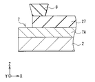
図7は、周辺領域4に設けられた端子領域6の詳細な構成を表すものであり、図1に示したVII−VII線に沿った断面構成を表している。基板2上の周辺領域4には、配線7Aが設けられており、この配線7Aを画素領域3から延在するパッシベーション膜27が覆っている。配線7Aは、例えばカソード電極15に電気的に接続されている。端子領域6では、この配線7Aがパッシベーション膜27から露出されている。換言すれば、パッシベーション膜27から露出された配線7Aが端子7を構成している。端子7には、例えばFPC(Flexible Printed Circuits)等(図示せず)が接続されている。図1には、基板2の2辺に端子領域6を設けた場合を示したが、端子領域6は基板2の1辺のみに設けるようにしてもよく、基板2の3辺に設けるようにしてもよい。基板2の全ての辺に端子領域6が配置されていてもよい。
FIG. 7 shows a detailed configuration of the
本実施の形態では、この端子7が配置された端子領域6と画素領域3との間に隔壁8が設けられている。詳細は後述するが、これにより、有機層14形成時に有機材料が画素領域3から端子領域6に流れ込むのを防ぐことができる。ここでは、画素領域3が本技術の有機層形成領域の一具体例であり、端子領域6が本技術の有機層非形成領域の一具体例である。
In the present embodiment, a
隔壁8は、例えばパッシベーション膜27上に設けられている。隔壁8の高さ(Z方向の距離)は例えば500nm〜4000nmであり、隔壁8の幅(図7のX方向の距離)は5μm〜100μmである。隔壁8は、周辺領域4のうち、例えば端子領域6に隣接した位置に設けられている。隔壁8は、例えばポリイミド系樹脂,アクリル系樹脂およびノボラック系樹脂等の有機材料により構成されている。画素間絶縁膜13に含まれる有機材料と同一の有機材料を用いて隔壁8を構成するようにしてもよい。隔壁8は撥液性を有していてもよい。例えば、上記有機材料にフッ素を混合することにより、撥液性の隔壁8を設けるようにしてもよい。あるいは、プラズマ処理あるいはフッ素加工処理により、撥液性の隔壁8を設けるようにしてもよい。
The
隔壁8は、画素領域3を囲むように設けるようにしてもよいが(図1)、図8に示したように、端子領域6が配置された基板2の辺に設けるようにしてもよい。
The
隔壁8の断面形状は例えば矩形状である(図7)。隔壁8は、テーパ形状あるいは逆テーパ形状を有していてもよい(図9,図10)。
The cross-sectional shape of the
基板2上の周辺領域4には、端子7に加えて、例えば、封止剤(後述の図16の封止剤19)およびカソード電極15が接続される配線(後述の図18の配線29)等が設けられている。
In the
[表示装置1の製造方法]
図11は、表示装置1の製造工程の一例を表したものである。上記のような表示装置1は、例えば次のようにして製造することができる(図12A〜図14B)。図12A,図13Aおよび図14Aは画素領域3の断面構成を表し、図12B,図13Bおよび図14Bは端子領域6近傍の断面構成を表している。
[Manufacturing Method of Display Device 1]
FIG. 11 shows an example of the manufacturing process of the
(TFT20および端子7の形成工程)
まず、基板2上の画素領域3に、所定の薄膜プロセスを経てゲート電極21、第1ゲート絶縁膜22、第2ゲート絶縁膜23、酸化物半導体膜24、チャネル保護膜25およびソース・ドレイン電極26をこの順に形成する。このとき、基板2上の周辺領域4には、配線7Aを形成しておく。次いで、基板2の全面にわたってパッシベーション膜27および平坦化膜28を、例えばスピンコート法またはスリットコート法により成膜する。続いて、成膜した平坦化膜28およびパッシベーション膜27を、例えばフォトリソグラフィ法により、所定の形状にパターニングして配線7Aの一部を露出させ、端子7を形成する(図12B)。
(Process for forming
First, the
(アノード電極12の形成工程(S101))
TFT20を設けた後、図12Aに示したように、有機EL素子10毎にアノード電極12を形成する。アノード電極12は、例えばAlNd合金をスパッタ法により基板2全面にわたって成膜した後、例えばフォトリソグラフィ法を用いてパターニングすることにより形成される。
(Formation process of anode electrode 12 (S101))
After the
(画素間絶縁膜13および隔壁8の形成工程(S102))
次いで、基板2全面にわたって例えばポリイミド系樹脂を成膜した後、これを所望の形状にパターニングする。これにより、画素領域3に画素間絶縁膜13が、周辺領域4に隔壁8が形成される(図13A,図13B)。
(Step of forming
Subsequently, for example, a polyimide resin film is formed over the entire surface of the
(有機層14およびカソード電極15の形成工程(S103,S104))
続いて、画素領域3に有機層14を形成する(図14A)。具体的には、例えば以下のようにして有機層14を形成する。まず、例えば真空蒸着法により、正孔注入層14Aおよび正孔輸送層14Bを、画素領域3の全面にわたって成膜する。真空蒸着法は、蒸着源から基板2に種々の材料を蒸着させる方法である。画素領域3の全面に有機層14を形成する場合には、蒸着源と基板2との間に、画素領域3と同一形状の開口を有するマスクを設けて蒸着を行う。正孔輸送層14Bを設けた後、赤色画素5Rに赤色発光層14CRを、緑色画素5Gに緑色発光層14CGを、青色画素5Bに青色発光層14CBをそれぞれ形成する。発光層14C(赤色発光層14CR、緑色発光層14CGおよび青色発光層14CB)は、例えばインクジェット印刷法、スリット印刷法、ストライプ印刷法およびノズル印刷法等の印刷法を用いて形成する。このような印刷法は、赤色発光層14CR、緑色発光層14CGまたは青色発光層14CBを構成する有機材料を有機溶媒に溶解させたインクを基板2上に塗布する方法である。インクの粘度は、例えば10cP以下である。発光層14Cを形成する際には、端子領域6等の発光層14Cを設けない領域を非接触式のマスク9で覆っておく(図14B)。マスク9は隔壁8も覆うように配置することが好ましい。本実施の形態では、周辺領域4に隔壁8を形成しているので、この隔壁8によりインクがせき止められる。したがって、画素領域3から端子領域6へインクが流れ込むのを防ぐことができる。青色発光層14CBは、赤色発光層14CRおよび緑色発光層14CGを形成した後、画素領域3の全面にわたって形成するようにしてもよい。発光層14Cとして、印刷法を用いて黄色発光層14CYおよび青色発光層14CBを形成するようにしてもよい(図6)。発光層14Cを設けた後、例えば真空蒸着法を用いて電子輸送層14D、電子注入層14E、カソード電極15および保護層をこの順に形成する。スパッタ法を用いてカソード電極15を形成するようにしてもよい。
(Formation process of
Subsequently, an
(封止基板17の形成工程)
封止基板17上には、例えば以下のようにして遮光膜およびカラーフィルタを形成する。まず、封止基板17の全面に遮光膜の構成材料を成膜したのち、これを例えばフォトリソグラフィ工程を用いてマトリクス状にパターニングし、画素5の配置に合わせた開口を複数形成する。これにより遮光膜が形成される。次いで、遮光膜の開口に赤フィルタ、緑フィルタおよび青フィルタを順次パターニングして設け、カラーフィルタを形成する。
(Formation process of sealing substrate 17)
On the sealing
(基板2と封止基板17との貼り合わせ工程)
上記のようにして形成した封止基板17は、例えばODF(One Drop Fill)工程により有機EL素子10および充てん層16を間にして、基板2に貼り合わされる。以上により、図1に示した表示装置1が完成する。
(Step of
The sealing
[表示装置1の動作]
表示装置1では、各有機EL素子10に、各色の映像信号に応じた駆動電流が印加されると、アノード電極12およびカソード電極15を通じて、有機層14に電子および正孔が注入される。これらの電子および正孔は、有機層14に含まれる発光層14Cにおいてそれぞれ再結合され、発光を生じる。この光はアノード電極12で反射され、カソード電極15,カラーフィルタおよび封止基板17を透過して外部へ取り出される。このようにして、表示装置1では、例えばR,G,Bのフルカラーの映像表示がなされる。
[Operation of display device 1]
In the
[表示装置1の作用・効果] [Operation and effect of display device 1]
ここで、表示装置1では、基板2上の画素領域3と端子領域6との間に隔壁8が設けられているので、有機層14を形成する際に、画素領域3から端子領域6へのインク(有機材料)の流れ込みを防ぐことができる。以下、これについて説明する。
Here, in the
真空蒸着法は、画素領域3全域にわたって有機層14を形成する場合には有用な方法であるが、真空蒸着法を用いて画素5毎に発光層14C等の有機層14を形成することは困難である。これは、マスクと基板2とのアラインメント、および材料の利用効率の低さ等が原因である。一方、印刷法は、画素5毎に有機層14を形成する場合にも、画素領域3全域に有機層14を形成する場合にも有用な方法である。特に、ノズル印刷法は安定して一定量のインクを塗布することができるため有機層14の形成に適している。ノズル印刷法は、ノズルからインクを常に吐出させ、有機材料を塗布する方法である。
The vacuum deposition method is a useful method when the
しかしながら、このような印刷法で使用するインクは粘度が低いので、画素領域3から周辺領域4にインクが流れ込みやすい。周辺領域4には、端子領域6等が設けられている。この端子領域6にインクが付着すると、端子7と外部の配線(例えばFPC)との電気的な接続を確保できず、歩留まりおよび信頼性等を損なう虞がある。
However, since the ink used in such a printing method has a low viscosity, the ink tends to flow from the
端子領域を有機材料の付着から保護する方法としては、例えば、粘着テープによる接触式のマスキングが提案されている(例えば特許文献1,2参照)。しかしながら、この方法では表示装置の構成部材に粘着剤が残存して、表示装置の信頼性を低下させる虞がある。また、粘着テープの縁にはインクのメニスカスが形成されるので、これに起因して、有機層に突起が生じる虞がある。なお、端子領域をマスキングせずに印刷法を用いることも考え得るが、例えば以下のような問題が生じる。ノズル印刷法は上記のように、有用な方法であるが、常時インクを吐出するため、マスキングせずに有機材料の付着を防ぐことはできない。インクジェト法は、所望の領域のみにインクを塗布しやすい方法であるが、画素毎に高い精度で有機層を形成するためには高価な装置が必要である。即ち、コストに影響する。スリット印刷法およびストライプ印刷法では、塗布領域の周縁部分での膜厚制御が困難であるので、これを考慮して画素領域よりも広い範囲にわたって有機層を形成する。このため、このインクの塗布領域よりも更に外側に端子領域を配置すると、所謂額縁領域が広くなり、表示装置の外観に影響を及ぼす虞がある。
As a method for protecting the terminal region from the adhesion of the organic material, for example, contact-type masking with an adhesive tape has been proposed (see, for example,
これに対し、表示装置1では、画素領域3と端子領域6との間に隔壁8が設けられているので、有機層14(発光層14C)を形成する際に画素領域3に塗布したインクは隔壁8でせき止められる。即ち、端子領域6よりも内側にインクがとどまり、画素領域3から端子領域6へのインクの流入が抑えられる。ノズル印刷法を用いることにより、均一な膜厚で有機層14を形成することができる。
In contrast, in the
また、粘着テープを使用しないので、粘着剤が残存せず、信頼性を維持できる。更に、粘着テープに起因した有機層の突起も形成されない。 Moreover, since no adhesive tape is used, no adhesive remains and reliability can be maintained. Furthermore, the protrusion of the organic layer resulting from the adhesive tape is not formed.
加えて、非接触式のマスク(例えば図14Bのマスク9)を用いて、ノズル印刷法、安価な装置によるインクジェット印刷法、スリット印刷法およびストライプ印刷法等を行うことができる。したがって、コストの上昇および額縁領域の増加を抑えることができる。
In addition, by using a non-contact mask (for example, the
以上のように本実施の形態では、基板2上に隔壁8を設けるようにしたので、有機層14を形成する際に、端子領域6への有機材料の付着を防止することが可能となる。よって、端子7と外部の配線との電気的な接続を確保し、表示装置1の歩留まりおよび信頼性等を向上させることが可能となる。
As described above, in the present embodiment, since the
また、隔壁8は画素領域3の画素間絶縁膜13と同一工程で形成することも可能であり、工程数の増加を抑えることができる。
Further, the
以下、上記第1の実施の形態の変形例および他の実施の形態について説明するが、上記第1の実施の形態における構成要素と同一のものには同一の符号を付し、適宜説明を省略する。 Hereinafter, modifications of the first embodiment and other embodiments will be described, but the same components as those in the first embodiment are denoted by the same reference numerals, and description thereof will be omitted as appropriate. To do.
<変形例1>
図15は、変形例1に係る表示装置(表示装置1A)の平面構成を表したものである。この表示装置1Aは、画素領域3と封止領域(封止領域18)との間に隔壁(隔壁8A)を有している。即ち、ここでは、封止領域18が本技術の有機層非形成領域の一具体例である。この点を除き、表示装置1Aは表示装置1と同様の構成を有し、その作用および効果も同様である。
<
FIG. 15 illustrates a planar configuration of a display device (display device 1A) according to the first modification. This display device 1A has a partition wall (
図16は、図15に示したA−A線に沿った断面構成を表している。基板2上の封止領域18には、封止剤19が設けられている。この封止剤19は、基板2と封止基板17とを接着するものであり、基板2と封止基板17との間の充てん層16の周囲に設けられている。即ち、封止領域18は、画素領域3を囲むように設けられている。封止剤19は、外部から画素領域3への水分の侵入を防ぐ役割も担っており、例えばエポキシ樹脂あるいはアクリル樹脂等により構成されている。
FIG. 16 shows a cross-sectional configuration along the line AA shown in FIG. A sealing
仮に、この封止領域18に有機層14(図4)の有機材料が付着した場合には、封止剤19と基板2との接着が阻まれ、封止強度が低下する。また、外部から画素領域3に水分が浸入しやすくなる。したがって、表示装置の信頼性を低下させる虞がある。
If the organic material of the organic layer 14 (FIG. 4) adheres to the sealing
表示装置1Aでは、画素領域3と封止領域18との間に隔壁8Aが設けられているので、有機層14(図4)を形成する際に、封止領域18への有機材料の付着を防止することが可能となる。よって、表示装置1Aの信頼性を維持することができる。隔壁8Aの構成材料、高さおよび幅等は上記隔壁8で説明したのと同様である。
In the display device 1A, since the
隔壁8Aの外側に隔壁8Bを設け、隔壁8Aと隔壁8Bとの間に封止領域18を配置するようにしてもよい。隔壁8Bは封止領域18の外側、即ち、周辺領域4のうち封止領域18と基板2の縁との間に設けられている。隔壁8Bは、隔壁8Aと同様の材料を用いて構成すればよく、例えば隔壁8Aと同程度の高さおよび幅を有している。このような隔壁8Bを設けることにより、仮に、封止領域18の外側にインクが付着した場合にも、封止領域18へのインクの流れ込みを防ぐことが可能となる。有機層14を形成する際には、封止領域18とともに隔壁8A,8Bを覆うマスク(図14Bのマスク9)が配置される。
A
<変形例2>
図17は、変形例2に係る表示装置(表示装置1B)の平面構成を表したものである。この表示装置1Bは、画素領域3と接続領域(接続領域15A)との間に隔壁8Aを有している。即ち、ここでは、接続領域15Aが本技術の有機層非形成領域の一具体例である。この点を除き、表示装置1Bは表示装置1と同様の構成を有し、その作用および効果も同様である。
<
FIG. 17 illustrates a planar configuration of a display device (display device 1B) according to the second modification. This display device 1B has a
図18は、図17に示したB−B線に沿った断面構成を表している。カソード電極15は、画素領域3から周辺領域4に延在しており、周辺領域4で配線29に電気的に接続されている。配線29は、例えば平坦化膜28上に設けられており、配線29とカソード電極15との間には絶縁膜31が介在している。周辺領域4に設けられた接続領域15Aでは、この絶縁膜31に接続孔が設けられており、この接続孔を介してカソード電極15と配線29とが接続されている。配線29は、例えば、共通電源供給線(GND)に電気的に接続されている。
FIG. 18 shows a cross-sectional configuration along the line BB shown in FIG. The
仮に、この接続領域15Aに有機層14(図4)の有機材料が付着した場合には、カソード電極15と配線29との電気的な接続を確保できず、歩留まりおよび信頼性等を損なう虞がある。
If the organic material of the organic layer 14 (FIG. 4) adheres to the
表示装置1Bでは、画素領域3と接続領域15Aとの間に隔壁8Aが設けられているので、有機層14(図4)を形成する際に、接続領域15Aへの有機材料の付着を防止することが可能となる。よって、表示装置1Bの歩留まりおよび信頼性等を維持することができる。上記表示装置1Aで説明したのと同様に、隔壁8Aの外側に隔壁8Bを設けて、隔壁8Aと隔壁8Bとの間に接続領域15Aを配置するようにしてもよい。このような隔壁8Bを設けることにより、仮に、接続領域15Aの外側にインクが付着した場合にも、接続領域15Aへのインクの流れ込みを防ぐことが可能となる。有機層14を形成する際には、接続領域15Aとともに隔壁8A,8Bを覆うマスク(図14Bのマスク9)が配置される。
In the display device 1B, since the
<変形例3>
図19は、変形例3に係る表示装置(表示装置1C)の要部の断面構成を表したものである。この表示装置1Cは、画素領域3に近い位置から順に、接続領域15A、封止領域18および端子領域6を有している。即ち、表示装置1Cは、周辺領域4に複数の有機層非形成領域を有している。この表示装置1Cでは、基板2上の画素領域3と接続領域15Aとの間、画素領域3と封止領域18との間、および画素領域3と端子領域6との間各々に隔壁(隔壁8または隔壁8A)が設けられている。詳細には、隔壁は、画素領域3と最も画素領域3に近い有機層非形成領域(接続領域15A)との間に加えて、隣り合う有機層非形成領域の間(接続領域15Aと封止領域18との間、および封止領域18と端子領域6との間)に設けられている。この点を除き、表示装置1Cは表示装置1と同様の構成を有し、その作用および効果も同様である。
<
FIG. 19 illustrates a cross-sectional configuration of a main part of a display device (display device 1C) according to
接続領域15Aおよび封止領域18では、隔壁8Aの外側に隔壁8Bが設けられている。即ち、接続領域15Aおよび封止領域18はそれぞれ、隔壁8Aと隔壁8Bとの間に設けられている。隔壁8Bを設けることにより、有機層14(図4)を形成する際に、仮に、接続領域15Aと封止領域18との間、または封止領域18と端子領域6との間にインク(有機材料)が付着した場合にも、接続領域15Aおよび封止領域18へのインクの流入を防ぐことができる。端子領域6の外側に更に、隔壁(図示せず)を設けて、隔壁間に端子領域6が配置されていてもよい。
In the
以下で説明する変形例4〜6(表示装置1D〜表示装置1F)は、上記表示装置1Cと同様に画素領域3に近い位置から順に、接続領域15A、封止領域18および端子領域6を有するものである。表示装置1D〜表示装置1Fでは、このうちのいずれか2つの領域と画素領域3の間に隔壁(隔壁8または隔壁8A)が配置されている。
Modified examples 4 to 6 (display device 1D to display device 1F) described below include a
<変形例4>
図20に示したように、表示装置1Dでは、画素領域3と封止領域18との間、および画素領域3と端子領域6との間に隔壁(隔壁8または隔壁8A)が設けられている。詳細には、隔壁は、接続領域15Aと封止領域18との間、および封止領域18と端子領域6との間に設けられている。封止領域18では、隔壁8Aの外側に隔壁8Bが設けられている。即ち、隔壁8Aと隔壁8Bとの間に封止領域18が配置されている。
<
As shown in FIG. 20, in the
<変形例5>
図21に示したように、表示装置1Eでは、画素領域3と接続領域15Aとの間、および画素領域3と端子領域6との間に隔壁(隔壁8または隔壁8A)が設けられている。詳細には、隔壁は、画素領域3と接続領域15Aとの間、および封止領域18と端子領域6との間に設けられている。接続領域15Aでは、隔壁8Aの外側に隔壁8Bが設けられている。即ち、隔壁8Aと隔壁8Bとの間に接続領域15Aが配置されている。
<
As shown in FIG. 21, in the display device 1E, a partition wall (a
<変形例6>
図22に示したように、表示装置1Fでは、画素領域3と接続領域15Aとの間、および画素領域3と封止領域18との間に隔壁8Aが設けられている。詳細には、隔壁8Aは、画素領域3と接続領域15Aとの間、および接続領域15Aと封止領域18との間に設けられている。この接続領域15Aおよび封止領域18では、隔壁8Aの外側に隔壁8Bが設けられている。即ち、接続領域15Aおよび封止領域18はそれぞれ、隔壁8Aと隔壁8Bとの間に配置されている。
<
As shown in FIG. 22, in the
<第2の実施の形態>
図23は本技術の第2の実施の形態に係る表示装置(表示装置30)の平面構成を表したものであり、図24は表示装置30の画素領域3の断面構成を表している。この表示装置30では、色毎の画素列5A(赤色画素列5AR,緑色画素列5AG,青色画素列5AB)の間に撥液領域(撥液領域13BR)が設けられている。この点を除き、表示装置30は表示装置1と同様の構成を有し、その作用および効果も同様である。
<Second Embodiment>
FIG. 23 illustrates a planar configuration of a display device (display device 30) according to the second embodiment of the present technology, and FIG. 24 illustrates a cross-sectional configuration of the
表示装置30では、有機層14の形成に例えばノズル印刷法、スリット印刷法またはストライプ印刷法等が用いられる。撥液領域13BRは、画素列5Aと同一方向に延在しており、有機層14の発光層(図5の発光層14C)を色別に塗布する際にインクのバンク(土手)として機能する。撥液領域13BRは、画素列5Aを区画(分割)するように、ライン状に設けられている。この撥液領域13BRにより、画素列5Aに吐出されたインクの過剰な濡れ広がりが抑えられ、隣接する画素列5Aへのインクの浸入を防ぐことができる。撥液領域13BRは、周辺領域4に延び、画素領域3を囲む枠状部分を有していることが好ましい。周辺領域4にも撥液領域13BRを設けることにより、例えば塗布開始時に周辺領域4に吐出されたインクの濡れ広がりが抑えられる。この枠状の撥液領域13BRの外側に、例えば隔壁8が設けられている。撥液領域13BRは、撥液層13B(図24)により形成されている。
In the display device 30, for example, a nozzle printing method, a slit printing method, or a stripe printing method is used for forming the
画素5の周囲は親液領域13ARとなっていることが好ましい。親液領域13ARは、インクの濡れ性を向上させるためのものであり、列方向に延在する撥液領域13BRと画素5との間および列方向に隣り合う画素5の間(行間領域)に設けられている。各画素5は親液領域13ARで囲まれている。親液領域13ARは、親液層13A(図24)により構成されている。
The periphery of the
周辺領域4の一部には、例えばビード形成領域4Aが設けられている。ビード形成領域4Aは、画素領域3を間にして対向する2辺に設けられている。有機層14を形成する際に、周辺領域4内の塗布開始位置にインクを吐出して液柱(ビード)を形成する領域である。このビード形成領域4Aには親液領域13ARが延在していることが好ましい。これにより、ビード形成領域4Aの濡れ性が向上し、ビードが形成されやすくなる。
For example, a
親液領域13ARを形成する親液層13Aは、有機EL素子10の発光領域を除き、画素領域3全域にわたって設けられている。周辺領域4のうち、ビード形成領域4Aにも親液層13Aが設けられていることが好ましい。親液層13Aは、平坦化膜28とアノード電極12の上面および側面とを覆っている。親液層13Aには、アノード電極12の上面を露出させる開口が設けられており、この親液層13Aの開口により有機EL素子10の発光領域が規定されるようになっている。親液層13Aの構成材料としては、例えば、酸化シリコン(SiO2)および窒化シリコン(Si3N4)等が挙げられる。
The
撥液領域13BRを構成する撥液層13Bは、親液層13A上に設けられ、親液層13A上の領域のうちの一部を覆っている。親液層13Aのうち、開口(有機EL素子10の発光領域)に隣接する領域は親液層13Aの表面が露出されている。親液層13Aとカソード電極15との間に設けられた撥液層13Bは、アノード電極12とカソード電極15との間の絶縁性を確保する役割を担っている。撥液層13Bの構成材料としては、例えば、ポリイミドおよびノボラック等の有機材料が挙げられる。有機材料に例えばプラズマ処理を施すことにより、撥液性を有する撥液層13Bが形成される。フッ素含有材料により撥液層13Bを構成するようにしてもよい。
The
(適用例)
続いて、図25ないし図39を参照して、上記第1,第2実施の形態および変形例に係る表示装置の適用例について説明する。上記実施の形態等の表示装置(表示装置1,1A,1B,1C,1D,1E,1F,30)は、テレビジョン装置,デジタルカメラ,ノート型パーソナルコンピュータ、携帯電話やスマートフォン等の携帯端末装置あるいはビデオカメラなどのあらゆる分野の電子機器に適用することが可能である。言い換えると、この表示装置は、外部から入力された映像信号あるいは内部で生成した映像信号を、画像あるいは映像として表示するあらゆる分野の電子機器に適用することが可能である。
(Application example)
Next, with reference to FIGS. 25 to 39, application examples of the display device according to the first and second embodiments and the modified examples will be described. The display devices (
(モジュール)
上記実施の形態等の表示装置は、例えば、図25に示したようなモジュールとして、後述する適用例1〜9などの種々の電子機器に組み込まれる。このモジュールは、例えば、基板2の画素領域3の周囲の周辺領域4に、配線を延長して外部接続用の端子(例えば図1の端子7)を形成したものである。この端子には、信号の入出力のためのフレキシブルプリント配線基板(FPC;Flexible Printed Circuit)9が接続されていてもよい。
(module)
The display device of the above-described embodiment or the like is incorporated into various electronic devices such as application examples 1 to 9 described later, for example, as a module as illustrated in FIG. In this module, for example, a terminal for external connection (for example, terminal 7 in FIG. 1) is formed by extending a wiring in a
(適用例1)
図26および図27は、電子ブック210の外観構成を表している。この電子ブック210は、例えば、表示部211および非表示部212と、操作部213とを備えている。なお、操作部213は、図26に示したように非表示部212の前面に設けられていてもよいし、図27に示したように非表示部212の上面に設けられていてもよい。表示部211が上記実施の形態等の表示装置により構成される。なお、上記実施の形態等の表示装置が、図26および図27に示した電子ブックと同様の構成を有するPDA(Personal Digital Assistants)などに搭載されてもよい。
(Application example 1)
26 and 27 show the external configuration of the
(適用例2)
図28および図29は、スマートフォン220の外観を表したものである。このスマートフォン220は、例えば、表側に表示部221および操作部222を有し、裏側にカメラ223を有しており、この表示部221が上記実施の形態等の表示装置により構成されている。
(Application example 2)
28 and 29 show the appearance of the
(適用例3)
図30は、上記実施の形態等の表示装置が適用されるテレビジョン装置230の外観を表したものである。このテレビジョン装置230は、例えば、フロントパネル231およびフィルターガラス232を含む映像表示画面部233を有している。映像表示画面部233が上記実施の形態等の表示装置により構成されている。
(Application example 3)
FIG. 30 illustrates an appearance of a television device 230 to which the display device of the above-described embodiment and the like is applied. The television device 230 includes, for example, a video display screen unit 233 including a front panel 231 and a filter glass 232. The video display screen unit 233 is configured by a display device such as the above embodiment.
(適用例4)
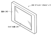
図31は、タブレットパーソナルコンピュータ240の外観を表したものである。このタブレットパーソナルコンピュータ240は、例えば、タッチパネル部241および筐体242を有しており、タッチパネル部241が上記実施の形態等の表示装置により構成されている。
(Application example 4)
FIG. 31 shows the appearance of the tablet personal computer 240. The tablet personal computer 240 has, for example, a touch panel unit 241 and a housing 242, and the touch panel unit 241 is configured by the display device of the above-described embodiment or the like.
(適用例5)
図32および図33は、デジタルスチルカメラ250の外観を表したものである。このデジタルスチルカメラ250は、例えば、フラッシュ用の発光部251、表示部252、メニュースイッチ253およびシャッターボタン254を有しており、表示部252が上記実施の形態等の表示装置により構成されている。
(Application example 5)
32 and 33 show the appearance of the digital
(適用例6)
図34は、ノートブック型パーソナルコンピュータ260の外観を表したものである。このノートブック型パーソナルコンピュータ260は、例えば、本体261,文字等の入力操作のためのキーボード262および画像を表示する表示部263を有しており、表示部263が上記実施の形態等の表示装置により構成されている。
(Application example 6)
FIG. 34 shows the appearance of the notebook personal computer 260. The notebook personal computer 260 includes, for example, a main body 261, a keyboard 262 for inputting characters and the like, and a display unit 263 that displays an image. The display unit 263 is a display device according to the above-described embodiment or the like. It is comprised by.
(適用例7)
図35は、ビデオカメラ270の外観を表したものである。このビデオカメラ270は、例えば、本体部271,この本体部271の前方側面に設けられた被写体撮影用のレンズ272,撮影時のスタート/ストップスイッチ273および表示部274を有している。表示部274が上記実施の形態等の表示装置により構成されている。
(Application example 7)
FIG. 35 shows the appearance of the video camera 270. The video camera 270 includes, for example, a main body 271, a
(適用例8)
図36および図37は、他の電子ブック280の外観を表したものである。電子ブック280は、柔らかい素材をコンポーネント化して形成された薄型のフレキシブルディスプレイである。この電子ブック280では、複数枚の紙(頁)を綴じて作られる実際の本のように、装置全体を閉じたり(折り畳んだり)、あるいは開いたりすることができるようになっている。ユーザは実際に本を読んでいるかのような感覚で、電子ブッ280クに表示された内容(例えば書籍の頁等)を閲覧することが可能である。
(Application example 8)
36 and 37 show the appearance of another
電子ブック280は、支持基板281上に、表示部282を備えたものであり、本における「背」の部分(背283A)には、ヒンジ部283を有している。この電子ブック280の下面(閉じたときに外側になる面)側には軟らかい樹脂フィルムよりなるカバー284が設けられ、上面(閉じたときに内側になる面)側は、柔らかく、かつ表示光に対して透明性を有する樹脂フィルムよりなる保護シート285により覆われている。表示部282が上記実施の形態等の表示装置により構成されている。
The
(適用例9)
図38および図39は、携帯電話機290の外観を表したものである。この携帯電話機290は、例えば、上側筐体291と下側筐体292とを連結部(ヒンジ部)293で連結したものであり、ディスプレイ294,サブディスプレイ295,ピクチャーライト296およびカメラ297を有している。ディスプレイ294またはサブディスプレイ295が上記実施の形態等の表示装置により構成されている。
(Application example 9)
38 and 39 show the appearance of the
以上、実施の形態および変形例を挙げて本技術を説明したが、本技術はこれら実施の形態に限定されるものではなく、種々変形が可能である。 As described above, the present technology has been described with reference to the embodiment and the modification. However, the present technology is not limited to the embodiment, and various modifications can be made.
例えば、上記実施の形態では、表示装置1,1A〜1F,30の構成を具体的に挙げて説明したが、表示装置1,1A〜1F,30は、図示した構成要素を全て備えるものに限定されるものではない。また、一部の構成要素を他の構成要素に置換することもできる。
For example, in the above-described embodiment, the configuration of the
また、上記実施の形態において説明した各層の材料および厚み、または成膜方法および成膜条件等は限定されるものではなく、他の材料および厚みとしてもよく、または他の成膜方法および成膜条件としてもよい。例えば、上記実施の形態では、TFT20におけるチャネルとして酸化物半導体を用いたが、これに限らず、シリコンまたは有機半導体等を用いてもよい。各部の構成材料に応じて、ドライプロセスとウェットプロセスとを併用することも可能である。
In addition, the material and thickness of each layer described in the above embodiment, the film formation method, the film formation conditions, and the like are not limited, and may be other materials and thicknesses, or other film formation methods and film formation. It is good also as conditions. For example, in the above embodiment, an oxide semiconductor is used as a channel in the
更にまた、上記実施の形態等では、発光層14C以外の有機層14を真空蒸着法を用いて形成する場合について説明したが、発光層14C以外の有機層14を印刷法を用いて形成するようにしてもよい。印刷法として、インクジェット法、ストライプ印刷法、スリット印刷法およびノズル印刷法に加えて、凸版印刷法、凹版印刷法、スクリーン印刷法およびマイクログラビアコート法等を用いるようにしてもよく、スピンコート法、ディッピング法、ドクターブレード法、吐出コート法およびスプレーコート法等の塗布法を用いて有機層14を形成するようにしてもよい。発光層14C以外の有機層14を画素5毎に形成するようにしてもよい。
Furthermore, in the above-described embodiment and the like, the case where the
なお、本明細書に記載された効果はあくまで例示であってこれに限定されるものではなく、また他の効果があってもよい。 In addition, the effect described in this specification is an illustration to the last, and is not limited to this, There may exist another effect.
なお、本技術は以下のような構成も取ることができる。
(1)有機層形成領域と、前記有機層形成領域の外側に設けられた有機層非形成領域とを有する第1基板と、前記第1基板上の前記有機層形成領域と前記有機層非形成領域との間に設けられた第1隔壁とを備えた表示装置。
(2)前記有機層非形成領域には、外部接続用の端子が設けられている前記(1)に記載の表示装置。
(3)前記第1基板と対向する第2基板を有し、前記有機層非形成領域には、前記第2基板と前記第1基板との間の封止剤が設けられている前記(1)に記載の表示装置。
(4)前記第1基板上の前記有機層形成領域には、第1電極および第2電極が設けられ、前記第2電極は、前記第1基板上の前記有機層非形成領域に設けられた配線に電気的に接続されている前記(1)に記載の表示装置。
(5)前記第1電極と前記第2電極との間には、発光層を含む有機層が設けられている前記(4)に記載の表示装置。
(6)前記第1基板上の前記前記有機層形成領域の外側に第2隔壁を有し、前記第1隔壁と前記第2隔壁との間に、前記有機層非形成領域が設けられている前記(1)乃至(5)のうちいずれか1つに記載の表示装置。
(7)前記第1基板には複数の前記有機層非形成領域が設けられるとともに、複数の前記第1隔壁を有し、複数の前記第1隔壁のうちの少なくとも一部は、隣り合う前記有機層非形成領域の間に設けられている前記(1)乃至(6)のうちいずれか1つに記載の表示装置。
(8)前記第1隔壁は、有機材料により構成されている前記(1)乃至(7)のうちいずれか1つに記載の表示装置。
(9)前記有機層形成領域は、行列状に配置された複数の画素を有する画素領域である前記(1)乃至(8)のうちいずれか1つに記載の表示装置。
(10)前記基板上の前記有機層形成領域に、画素間絶縁膜を有し、前記画素間絶縁膜は、前記第1隔壁の構成材料と同一の材料を含んでいる前記(9)に記載の表示装置。
(11)前記複数の画素の列間領域に撥液領域を有している前記(9)または(10)に記載の表示装置。
(12)表示装置を備え、前記表示装置は、有機層形成領域と、前記有機層形成領域の外側に設けられた有機層非形成領域とを有する第1基板と、前記第1基板上の前記有機層形成領域と前記有機層非形成領域との間に設けられた第1隔壁とを含む電子機器。
In addition, this technique can also take the following structures.
(1) A first substrate having an organic layer forming region and an organic layer non-forming region provided outside the organic layer forming region, and the organic layer forming region and the organic layer non-forming on the first substrate A display device comprising: a first partition wall provided between the region.
(2) The display device according to (1), wherein a terminal for external connection is provided in the organic layer non-formation region.
(3) The first substrate has a second substrate facing the first substrate, and the organic layer non-formation region is provided with a sealant between the second substrate and the first substrate. ) Display device.
(4) A first electrode and a second electrode are provided in the organic layer forming region on the first substrate, and the second electrode is provided in the organic layer non-forming region on the first substrate. The display device according to (1), which is electrically connected to the wiring.
(5) The display device according to (4), wherein an organic layer including a light emitting layer is provided between the first electrode and the second electrode.
(6) A second partition is provided outside the organic layer forming region on the first substrate, and the organic layer non-forming region is provided between the first partition and the second partition. The display device according to any one of (1) to (5).
(7) The first substrate is provided with a plurality of organic layer non-formation regions and has a plurality of the first partition walls, and at least a part of the plurality of first partition walls is adjacent to the organic The display device according to any one of (1) to (6) provided between the layer non-formation regions.
(8) The display device according to any one of (1) to (7), wherein the first partition is made of an organic material.
(9) The display device according to any one of (1) to (8), wherein the organic layer formation region is a pixel region having a plurality of pixels arranged in a matrix.
(10) The organic layer formation region on the substrate has an inter-pixel insulating film, and the inter-pixel insulating film contains the same material as the constituent material of the first partition. Display device.
(11) The display device according to (9) or (10), wherein a liquid repellent region is provided in an inter-column region of the plurality of pixels.
(12) A display device is provided, the display device including a first substrate having an organic layer formation region and an organic layer non-formation region provided outside the organic layer formation region, and the first substrate on the first substrate. An electronic device including an organic layer forming region and a first partition provided between the organic layer non-forming region.
1,1A,1B,1C,1D,1E,1F,30・・・表示装置、10・・・有機EL素子、10R・・・赤色有機EL素子、10G・・・緑色有機EL素子、10B・・・青色有機EL素子、2・・・基板、3・・・画素領域、4・・・周辺領域、5・・・画素、5R・・・赤色画素、5G・・・緑色画素、5B・・・青色画素、6・・・端子領域、7・・・端子、8,8A,8B・・・隔壁、12・・・アノード電極、13・・・画素間絶縁膜、14・・・有機層、15・・・カソード電極、15A・・・接続領域、16・・・充てん層、17・・・封止基板、18・・・封止領域、19・・・封止剤、20・・・TFT、21・・・ゲート電極、22・・・第1ゲート絶縁膜、23・・・第2ゲート絶縁膜、24・・・酸化物半導体層、25・・・チャネル保護膜、26・・・ソース・ドレイン電極、27・・・パッシベーション膜、28・・・平坦化膜、29・・・配線、31・・・絶縁層。 1, 1A, 1B, 1C, 1D, 1E, 1F, 30 ... display device, 10 ... organic EL element, 10R ... red organic EL element, 10G ... green organic EL element, 10B. -Blue organic EL element, 2 ... substrate, 3 ... pixel region, 4 ... peripheral region, 5 ... pixel, 5R ... red pixel, 5G ... green pixel, 5B ... Blue pixel, 6 ... terminal region, 7 ... terminal, 8, 8A, 8B ... partition wall, 12 ... anode electrode, 13 ... inter-pixel insulating film, 14 ... organic layer, 15 ... Cathode electrode, 15A ... Connection region, 16 ... Packing layer, 17 ... Sealing substrate, 18 ... Sealing region, 19 ... Sealing agent, 20 ... TFT, 21 ... Gate electrode, 22 ... First gate insulating film, 23 ... Second gate insulating film, 24 ... Oxide semiconductor layer 25 ... channel protective film, 26 ... drain electrode, 27 ... passivation film, 28 ... flattening film, 29 ... wiring, 31 ... insulating layer.
Claims (11)
前記第1基板上の前記有機層形成領域に設けられた第1電極と、
前記第1電極に対向する第2電極と、
前記第1基板上の前記有機層非形成領域に設けられた配線と、
前記第1基板上の前記有機層形成領域と前記有機層非形成領域との間に設けられた第1隔壁と、
前記第1基板上の前記有機層形成領域の外側に設けられた第2隔壁とを備え、
前記第1隔壁と前記第2隔壁との間に、前記有機層非形成領域が設けられ、
前記第1隔壁および前記第2隔壁の高さは500nm〜4000nmであり、
前記第2電極は、前記有機層形成領域から前記有機層非形成領域に延在し、前記第1隔壁と前記第2隔壁との間で前記配線に接続されている
表示装置。 A first substrate having an organic layer formation region and an organic layer non-formation region provided outside the organic layer formation region;
A first electrode provided in the organic layer forming region on the first substrate;
A second electrode facing the first electrode;
Wiring provided in the organic layer non-formation region on the first substrate;
A first partition provided between the organic layer forming region and the organic layer non-forming region on the first substrate;
A second partition provided outside the organic layer forming region on the first substrate,
The organic layer non-formation region is provided between the first partition and the second partition,
The height of the first partition wall and the second partition wall Ri 500nm~4000nm der,
The display device , wherein the second electrode extends from the organic layer formation region to the organic layer non-formation region and is connected to the wiring between the first partition and the second partition .
請求項1に記載の表示装置。 The display device according to claim 1, wherein a terminal for external connection is provided outside the organic layer forming region .
前記有機層形成領域の外側には、前記第2基板と前記第1基板との間の封止剤が設けられている
請求項1または請求項2に記載の表示装置。 A second substrate facing the first substrate with the first electrode and the second electrode in between ,
The display device according to claim 1 , wherein a sealant between the second substrate and the first substrate is provided outside the organic layer forming region .
請求項3に記載の表示装置。 The display device according to claim 3, wherein the first partition and the second partition are not in contact with the second substrate.
請求項1ないし請求項4のうちいずれか1項に記載の表示装置。 An organic layer including a light emitting layer is provided between the first electrode and the second electrode.
The display device according to any one of claims 1 to 4 .
複数の前記第1隔壁のうちの少なくとも一部は、隣り合う前記有機層非形成領域の間に設けられている
請求項1ないし請求項5のうちいずれか1項に記載の表示装置。 The first substrate is provided with a plurality of organic layer non-formation regions and a plurality of first partition walls,
6. The display device according to claim 1, wherein at least a part of the plurality of first partition walls is provided between the adjacent organic layer non-formation regions.
請求項1ないし請求項6のうちいずれか1項に記載の表示装置。 It said first septum and said second septum claims 1 and is made of an organic material display device according to any one of claims 6.
請求項1ないし請求項7のうちいずれか1項に記載の表示装置。 The display device according to claim 1, wherein the organic layer formation region is a pixel region having a plurality of pixels arranged in a matrix.
前記画素間絶縁膜は、前記第1隔壁および前記第2隔壁の構成材料と同一の材料を含んでいる
請求項8に記載の表示装置。 An inter-pixel insulating film in the organic layer forming region on the first substrate;
The inter-pixel insulating film includes the same material as the constituent material of the first partition and the second partition.
The display device according to claim 8 .
請求項8または請求項9に記載の表示装置。 A liquid repellent area is provided in an inter-column area of the plurality of pixels.
The display device according to claim 8 or 9 .
前記表示装置は、
有機層形成領域と、前記有機層形成領域の外側に設けられた有機層非形成領域とを有する第1基板と、
前記第1基板上の前記有機層形成領域に設けられた第1電極と、
前記第1電極に対向する第2電極と、
前記第1基板上の前記有機層非形成領域に設けられた配線と、
前記第1基板上の前記有機層形成領域と前記有機層非形成領域との間に設けられた第1隔壁と、
前記第1基板上の前記有機層形成領域の外側に設けられた第2隔壁とを含み、
前記第1隔壁と前記第2隔壁との間に、前記有機層非形成領域が設けられ、
前記第1隔壁および前記第2隔壁の高さは500nm〜4000nmであり、
前記第2電極は、前記有機層形成領域から前記有機層非形成領域に延在し、前記第1隔壁と前記第2隔壁との間で前記配線に接続されている
電子機器。 A display device,
The display device
A first substrate having an organic layer formation region and an organic layer non-formation region provided outside the organic layer formation region;
A first electrode provided in the organic layer forming region on the first substrate;
A second electrode facing the first electrode;
Wiring provided in the organic layer non-formation region on the first substrate;
A first partition provided between the organic layer forming region and the organic layer non-forming region on the first substrate;
A second partition provided outside the organic layer forming region on the first substrate,
The organic layer non-formation region is provided between the first partition and the second partition,
The height of the first partition wall and the second partition wall Ri 500nm~4000nm der,
The second electrode extends from the organic layer formation region to the organic layer non-formation region, and is connected to the wiring between the first partition and the second partition .
Priority Applications (2)
| Application Number | Priority Date | Filing Date | Title |
|---|---|---|---|
| JP2014044807A JP6439114B2 (en) | 2014-03-07 | 2014-03-07 | Display device and electronic device |
| US14/626,145 US9484394B2 (en) | 2014-03-07 | 2015-02-19 | Display device and electronic apparatus |
Applications Claiming Priority (1)
| Application Number | Priority Date | Filing Date | Title |
|---|---|---|---|
| JP2014044807A JP6439114B2 (en) | 2014-03-07 | 2014-03-07 | Display device and electronic device |
Publications (3)
| Publication Number | Publication Date |
|---|---|
| JP2015170493A JP2015170493A (en) | 2015-09-28 |
| JP2015170493A5 JP2015170493A5 (en) | 2017-02-23 |
| JP6439114B2 true JP6439114B2 (en) | 2018-12-19 |
Family
ID=54018275
Family Applications (1)
| Application Number | Title | Priority Date | Filing Date |
|---|---|---|---|
| JP2014044807A Active JP6439114B2 (en) | 2014-03-07 | 2014-03-07 | Display device and electronic device |
Country Status (2)
| Country | Link |
|---|---|
| US (1) | US9484394B2 (en) |
| JP (1) | JP6439114B2 (en) |
Families Citing this family (7)
| Publication number | Priority date | Publication date | Assignee | Title |
|---|---|---|---|---|
| TWI580014B (en) * | 2013-09-20 | 2017-04-21 | Joled Inc | Display devices and electronic machines |
| JP6816102B2 (en) * | 2016-03-01 | 2021-01-20 | パイオニア株式会社 | Manufacturing method of light emitting device |
| JP6640034B2 (en) * | 2016-06-17 | 2020-02-05 | 株式会社ジャパンディスプレイ | Manufacturing method of organic EL display device |
| CN108281571B (en) * | 2018-03-30 | 2024-03-12 | 京东方科技集团股份有限公司 | Electrode exhaust structure, electrode, display panel and display device |
| CN110767823B (en) * | 2018-07-27 | 2021-01-22 | 京东方科技集团股份有限公司 | Flexible display panel and display device |
| CN109087935B (en) * | 2018-08-20 | 2021-09-10 | 京东方科技集团股份有限公司 | Display substrate, preparation method thereof and display panel |
| US20230209924A1 (en) * | 2020-05-20 | 2023-06-29 | Sharp Kabushiki Kaisha | Display device and display device production method |
Family Cites Families (13)
| Publication number | Priority date | Publication date | Assignee | Title |
|---|---|---|---|---|
| JP4114895B2 (en) * | 1998-07-08 | 2008-07-09 | Tdk株式会社 | Organic EL display device |
| TWI352553B (en) * | 2002-12-26 | 2011-11-11 | Semiconductor Energy Lab | Light emitting device and a method for manufacturi |
| JP4479381B2 (en) * | 2003-09-24 | 2010-06-09 | セイコーエプソン株式会社 | Electro-optical device, method of manufacturing electro-optical device, and electronic apparatus |
| JP3951055B2 (en) * | 2004-02-18 | 2007-08-01 | セイコーエプソン株式会社 | Organic electroluminescence device and electronic device |
| JP4486840B2 (en) * | 2004-03-26 | 2010-06-23 | オプトレックス株式会社 | Display device and manufacturing method thereof |
| JP2007094312A (en) * | 2005-09-30 | 2007-04-12 | Toppan Printing Co Ltd | Print and its manufacturing method |
| JP2007317546A (en) * | 2006-05-26 | 2007-12-06 | Optrex Corp | Organic el display device, and manufacturing method of organic el display device |
| JP2008000678A (en) | 2006-06-22 | 2008-01-10 | Dainippon Screen Mfg Co Ltd | Mask member, coating apparatus, coating system and coating method |
| JP5226379B2 (en) | 2008-04-30 | 2013-07-03 | 大日本スクリーン製造株式会社 | Tape sticking device, coating system and masking tape |
| JP5168121B2 (en) * | 2008-12-12 | 2013-03-21 | カシオ計算機株式会社 | LIGHT EMITTING PANEL AND METHOD FOR MANUFACTURING LIGHT EMITTING PANEL |
| KR100993415B1 (en) * | 2009-03-24 | 2010-11-09 | 삼성모바일디스플레이주식회사 | Organic light emitting display device |
| JP6142191B2 (en) * | 2011-05-19 | 2017-06-07 | 株式会社Joled | Display device and electronic device |
| JP2013214496A (en) * | 2012-03-08 | 2013-10-17 | Seiko Epson Corp | Method for manufacturing organic el device, organic el device, and electronic apparatus |
-
2014
- 2014-03-07 JP JP2014044807A patent/JP6439114B2/en active Active
-
2015
- 2015-02-19 US US14/626,145 patent/US9484394B2/en active Active
Also Published As
| Publication number | Publication date |
|---|---|
| US20150255743A1 (en) | 2015-09-10 |
| JP2015170493A (en) | 2015-09-28 |
| US9484394B2 (en) | 2016-11-01 |
Similar Documents
| Publication | Publication Date | Title |
|---|---|---|
| US11800741B2 (en) | Display unit with moisture proof film outside of seal section and electronic apparatus with said display unit | |
| US9147860B2 (en) | Light emitting device, method of manufacturing the light emitting device, and display unit | |
| JP6439114B2 (en) | Display device and electronic device | |
| US9123674B2 (en) | Display unit, method of manufacturing display unit, and electronic apparatus | |
| JP5808624B2 (en) | Display device and electronic device | |
| US9231037B2 (en) | Display unit and electronic apparatus | |
| US10539849B2 (en) | Color change member, light emitting device, display device and electronic apparatus | |
| US10707446B2 (en) | Display unit and electronic apparatus | |
| US20150090983A1 (en) | Display unit and electronic apparatus | |
| TWI580014B (en) | Display devices and electronic machines | |
| US8872200B2 (en) | Display device and electronic apparatus | |
| US8624233B2 (en) | Organic electroluminescence display device and electronic apparatus | |
| US9859528B2 (en) | Display and electronic apparatus | |
| JP2012256587A (en) | Display device and electronic apparatus | |
| JP2013065405A (en) | Display device and manufacturing method therefor | |
| US20240023366A1 (en) | Display unit with moisture proof film outside of seal section and electronic apparatus with said display unit |
Legal Events
| Date | Code | Title | Description |
|---|---|---|---|
| A521 | Request for written amendment filed |
Free format text: JAPANESE INTERMEDIATE CODE: A523 Effective date: 20161216 |
|
| A621 | Written request for application examination |
Free format text: JAPANESE INTERMEDIATE CODE: A621 Effective date: 20161216 |
|
| A977 | Report on retrieval |
Free format text: JAPANESE INTERMEDIATE CODE: A971007 Effective date: 20170913 |
|
| A131 | Notification of reasons for refusal |
Free format text: JAPANESE INTERMEDIATE CODE: A131 Effective date: 20170926 |
|
| A521 | Request for written amendment filed |
Free format text: JAPANESE INTERMEDIATE CODE: A523 Effective date: 20171110 |
|
| A131 | Notification of reasons for refusal |
Free format text: JAPANESE INTERMEDIATE CODE: A131 Effective date: 20180213 |
|
| A521 | Request for written amendment filed |
Free format text: JAPANESE INTERMEDIATE CODE: A523 Effective date: 20180413 |
|
| TRDD | Decision of grant or rejection written | ||
| A01 | Written decision to grant a patent or to grant a registration (utility model) |
Free format text: JAPANESE INTERMEDIATE CODE: A01 Effective date: 20180918 |
|
| A61 | First payment of annual fees (during grant procedure) |
Free format text: JAPANESE INTERMEDIATE CODE: A61 Effective date: 20181015 |
|
| R150 | Certificate of patent or registration of utility model |
Ref document number: 6439114 Country of ref document: JP Free format text: JAPANESE INTERMEDIATE CODE: R150 |
|
| R250 | Receipt of annual fees |
Free format text: JAPANESE INTERMEDIATE CODE: R250 |
|
| R250 | Receipt of annual fees |
Free format text: JAPANESE INTERMEDIATE CODE: R250 |
|
| S303 | Written request for registration of pledge or change of pledge |
Free format text: JAPANESE INTERMEDIATE CODE: R316303 |
|
| R350 | Written notification of registration of transfer |
Free format text: JAPANESE INTERMEDIATE CODE: R350 |
|
| S803 | Written request for registration of cancellation of provisional registration |
Free format text: JAPANESE INTERMEDIATE CODE: R316803 |
|
| R350 | Written notification of registration of transfer |
Free format text: JAPANESE INTERMEDIATE CODE: R350 |
|
| R250 | Receipt of annual fees |
Free format text: JAPANESE INTERMEDIATE CODE: R250 |
|
| S111 | Request for change of ownership or part of ownership |
Free format text: JAPANESE INTERMEDIATE CODE: R313113 |