JP6437875B2 - Optical waveguide device and manufacturing method thereof - Google Patents
Optical waveguide device and manufacturing method thereof Download PDFInfo
- Publication number
- JP6437875B2 JP6437875B2 JP2015086787A JP2015086787A JP6437875B2 JP 6437875 B2 JP6437875 B2 JP 6437875B2 JP 2015086787 A JP2015086787 A JP 2015086787A JP 2015086787 A JP2015086787 A JP 2015086787A JP 6437875 B2 JP6437875 B2 JP 6437875B2
- Authority
- JP
- Japan
- Prior art keywords
- opening
- cladding layer
- light emitting
- optical
- layer
- Prior art date
- Legal status (The legal status is an assumption and is not a legal conclusion. Google has not performed a legal analysis and makes no representation as to the accuracy of the status listed.)
- Active
Links
Images


Classifications
-
- G—PHYSICS
- G02—OPTICS
- G02B—OPTICAL ELEMENTS, SYSTEMS OR APPARATUS
- G02B6/00—Light guides; Structural details of arrangements comprising light guides and other optical elements, e.g. couplings
- G02B6/24—Coupling light guides
- G02B6/42—Coupling light guides with opto-electronic elements
- G02B6/4201—Packages, e.g. shape, construction, internal or external details
- G02B6/4204—Packages, e.g. shape, construction, internal or external details the coupling comprising intermediate optical elements, e.g. lenses, holograms
- G02B6/4214—Packages, e.g. shape, construction, internal or external details the coupling comprising intermediate optical elements, e.g. lenses, holograms the intermediate optical element having redirecting reflective means, e.g. mirrors, prisms for deflecting the radiation from horizontal to down- or upward direction toward a device
-
- G—PHYSICS
- G02—OPTICS
- G02B—OPTICAL ELEMENTS, SYSTEMS OR APPARATUS
- G02B6/00—Light guides; Structural details of arrangements comprising light guides and other optical elements, e.g. couplings
- G02B6/10—Light guides; Structural details of arrangements comprising light guides and other optical elements, e.g. couplings of the optical waveguide type
- G02B6/12—Light guides; Structural details of arrangements comprising light guides and other optical elements, e.g. couplings of the optical waveguide type of the integrated circuit kind
- G02B6/122—Basic optical elements, e.g. light-guiding paths
-
- G—PHYSICS
- G02—OPTICS
- G02B—OPTICAL ELEMENTS, SYSTEMS OR APPARATUS
- G02B6/00—Light guides; Structural details of arrangements comprising light guides and other optical elements, e.g. couplings
- G02B6/10—Light guides; Structural details of arrangements comprising light guides and other optical elements, e.g. couplings of the optical waveguide type
- G02B6/12—Light guides; Structural details of arrangements comprising light guides and other optical elements, e.g. couplings of the optical waveguide type of the integrated circuit kind
- G02B6/13—Integrated optical circuits characterised by the manufacturing method
- G02B6/138—Integrated optical circuits characterised by the manufacturing method by using polymerisation
-
- H—ELECTRICITY
- H05—ELECTRIC TECHNIQUES NOT OTHERWISE PROVIDED FOR
- H05K—PRINTED CIRCUITS; CASINGS OR CONSTRUCTIONAL DETAILS OF ELECTRIC APPARATUS; MANUFACTURE OF ASSEMBLAGES OF ELECTRICAL COMPONENTS
- H05K1/00—Printed circuits
- H05K1/02—Details
- H05K1/0274—Optical details, e.g. printed circuits comprising integral optical means
-
- G—PHYSICS
- G02—OPTICS
- G02B—OPTICAL ELEMENTS, SYSTEMS OR APPARATUS
- G02B6/00—Light guides; Structural details of arrangements comprising light guides and other optical elements, e.g. couplings
- G02B6/10—Light guides; Structural details of arrangements comprising light guides and other optical elements, e.g. couplings of the optical waveguide type
- G02B6/12—Light guides; Structural details of arrangements comprising light guides and other optical elements, e.g. couplings of the optical waveguide type of the integrated circuit kind
- G02B2006/12083—Constructional arrangements
- G02B2006/12121—Laser
-
- G—PHYSICS
- G02—OPTICS
- G02B—OPTICAL ELEMENTS, SYSTEMS OR APPARATUS
- G02B6/00—Light guides; Structural details of arrangements comprising light guides and other optical elements, e.g. couplings
- G02B6/10—Light guides; Structural details of arrangements comprising light guides and other optical elements, e.g. couplings of the optical waveguide type
- G02B6/12—Light guides; Structural details of arrangements comprising light guides and other optical elements, e.g. couplings of the optical waveguide type of the integrated circuit kind
- G02B2006/12083—Constructional arrangements
- G02B2006/12123—Diode
-
- G—PHYSICS
- G02—OPTICS
- G02B—OPTICAL ELEMENTS, SYSTEMS OR APPARATUS
- G02B6/00—Light guides; Structural details of arrangements comprising light guides and other optical elements, e.g. couplings
- G02B6/24—Coupling light guides
- G02B6/42—Coupling light guides with opto-electronic elements
- G02B6/4201—Packages, e.g. shape, construction, internal or external details
- G02B6/4219—Mechanical fixtures for holding or positioning the elements relative to each other in the couplings; Alignment methods for the elements, e.g. measuring or observing methods especially used therefor
- G02B6/4228—Passive alignment, i.e. without a detection of the degree of coupling or the position of the elements
- G02B6/4232—Passive alignment, i.e. without a detection of the degree of coupling or the position of the elements using the surface tension of fluid solder to align the elements, e.g. solder bump techniques
-
- G—PHYSICS
- G02—OPTICS
- G02B—OPTICAL ELEMENTS, SYSTEMS OR APPARATUS
- G02B6/00—Light guides; Structural details of arrangements comprising light guides and other optical elements, e.g. couplings
- G02B6/24—Coupling light guides
- G02B6/42—Coupling light guides with opto-electronic elements
- G02B6/4201—Packages, e.g. shape, construction, internal or external details
- G02B6/4274—Electrical aspects
- G02B6/428—Electrical aspects containing printed circuit boards [PCB]
-
- G—PHYSICS
- G02—OPTICS
- G02B—OPTICAL ELEMENTS, SYSTEMS OR APPARATUS
- G02B6/00—Light guides; Structural details of arrangements comprising light guides and other optical elements, e.g. couplings
- G02B6/24—Coupling light guides
- G02B6/42—Coupling light guides with opto-electronic elements
- G02B6/43—Arrangements comprising a plurality of opto-electronic elements and associated optical interconnections
Description
本発明は、光導波路装置及びその製造方法に関する。 The present invention relates to an optical waveguide device and a method for manufacturing the same.
従来、電気信号を扱う配線基板の上に光信号を扱う光導波路が形成された光導波路装置がある。光導波路装置は光電気複合基板であり、電気信号の伝達速度の限界を補うために、高速部分を光信号で伝達することができる。 Conventionally, there is an optical waveguide device in which an optical waveguide that handles optical signals is formed on a wiring board that handles electrical signals. The optical waveguide device is a photoelectric composite substrate, and can transmit a high-speed portion with an optical signal in order to compensate for the limit of the transmission speed of an electric signal.
光導波路の端側には光路変換ミラーが配置されており、光素子が光導波路の光路変換ミラーに光結合されるように配線基板に実装される。 An optical path conversion mirror is disposed on the end side of the optical waveguide, and the optical element is mounted on the wiring board so as to be optically coupled to the optical path conversion mirror of the optical waveguide.
後述する予備的事項の欄で説明するように、下側に突出する発光部を備えた発光素子を光導波路のクラッド層の上に搭載すると、発光素子の発光部がクラッド層及び光路変換ミラーを下側に押し込んだ状態となる。 As will be described in the preliminary section described later, when a light emitting device having a light emitting portion protruding downward is mounted on a cladding layer of an optical waveguide, the light emitting portion of the light emitting device has a cladding layer and an optical path conversion mirror. It will be in the state pushed down.
このため、光導波路の光路変換ミラーが変形して傾斜角度がずれることがある。その結果、発光素子と光路変換ミラーとの光結合の特性が劣化し、高い信頼性を得られなくなる課題がある。 For this reason, the optical path conversion mirror of the optical waveguide may be deformed to shift the tilt angle. As a result, there is a problem in that the characteristics of optical coupling between the light emitting element and the optical path conversion mirror deteriorate, and high reliability cannot be obtained.
下側に突出する発光部又は受光部を備えた光素子を信頼性よく搭載できる構造の光導波路装置及びその製造方法を提供することを目的とする。 An object of the present invention is to provide an optical waveguide device having a structure in which an optical element including a light emitting portion or a light receiving portion protruding downward can be mounted with high reliability, and a method for manufacturing the same.
以下の開示の一観点によれば、配線基板と、前記配線基板の上面に形成された接続パッドと、前記配線基板の上に、第1クラッド層、コア層及び第2クラッド層が順に形成された光導波路と、前記コア層に形成された光路変換ミラーと、前記接続パッドの上の前記第1クラッド層に形成されたコンタクトホールと、前記第2クラッド層に形成され、前記光路変換ミラー上の領域に配置された第1開口部と、前記第1開口部に繋がって前記コンタクトホールに連通する第2開口部とを備えた開口部と、前記第2クラッド層の上に、少なくとも一端が前記第2開口部の内側に配置され、前記第2開口部の一部が露出するように搭載された光素子と、前記第2クラッド層の前記第1開口部内に配置され、前記光素子の下側に突出する発光部又は受光部と、前記第2クラッド層の開口部に充填されたアンダーフィル樹脂とを有し、前記光素子の接続端子が前記コンタクトホール内の前記接続パッドに接続され、前記第2クラッド層の開口部及び前記コンタクトホールに前記アンダーフィル樹脂が充填されている光導波路装置が提供される。
According to one aspect of the following disclosure, a wiring board, a connection pad formed on the upper surface of the wiring board, and a first cladding layer, a core layer, and a second cladding layer are sequentially formed on the wiring board. An optical waveguide, an optical path conversion mirror formed in the core layer, a contact hole formed in the first cladding layer on the connection pad, and an optical path conversion mirror formed in the second cladding layer. At least one end on the second clad layer, and an opening having a first opening disposed in the region, a second opening connected to the first opening and communicating with the contact hole, and the second is placed inside the opening, the an optical element mounted so that to expose a portion of the second opening, disposed within said first opening of said second cladding layer, the optical element Light emitting part or light receiving projecting downward And an underfill resin filled in the opening of the second cladding layer, wherein the connection terminal of the optical element is connected to the connection pad in the contact hole, and the opening of the second cladding layer and An optical waveguide device in which the contact hole is filled with the underfill resin is provided.
また、その開示のその他の観点によれば、上面に接続パッドを備えた配線基板を用意する工程と、前記配線基板の上に第1クラッド層を形成する工程と、前記第1クラッド層の上にコア層を形成する工程と、前記コア層に光路変換ミラーを形成する工程と、前記第1クラッド層及び前記コア層の上に第2クラッド層を形成する工程とを有し、前記接続パッドの上の前記第1クラッド層にコンタクトホールが形成され、かつ、前記第2クラッド層に、前記光路変換ミラー上の領域に配置された第1開口部と、前記第1開口部に繋がって前記コンタクトホールに連通する第2開口部とを備えた開口部が形成された構造が得られ、前記第2クラッド層を形成する工程の後に、下側から突出する発光部又は受光部を備えた光素子を用意する工程と、前記発光部又は受光部が前記第2クラッド層の前記第1開口部内に配置され、かつ前記光素子の少なくとも一端が前記第2開口部の内側に配置され、かつ前記第2開口部の一部が露出するように、前記第2クラッド層の上に前記光素子を搭載する工程と、前記第2クラッド層の開口部にアンダーフィル樹脂を充填する工程とを有し、前記光素子の接続端子が前記コンタクトホール内の前記接続パッドに接続され、前記第2クラッド層の開口部及び前記コンタクトホールに前記アンダーフィル樹脂が充填される光導波路装置の製造方法が提供される。
According to another aspect of the disclosure, a step of preparing a wiring board having a connection pad on an upper surface, a step of forming a first cladding layer on the wiring board, and a top of the first cladding layer Forming a core layer, forming an optical path conversion mirror on the core layer, and forming a second cladding layer on the first cladding layer and the core layer, and the connection pad A contact hole is formed in the first clad layer above the first clad layer, and the second clad layer is connected to the first opening and a first opening disposed in a region on the optical path conversion mirror. Light having a light emitting part or a light receiving part protruding from the lower side after the step of forming the second cladding layer is obtained after the structure having the second opening part communicating with the contact hole is formed. Before preparing the element and before Emitting portion or the light receiving portion is disposed within said first opening of said second cladding layer, and at least one end of the optical elements are arranged on the inner side of the second opening, and part of the second opening in so that to expose the the step of mounting the optical element on the second cladding layer, and a step of filling an underfill resin into the opening of the second cladding layer, the connection terminals of the optical element Is connected to the connection pad in the contact hole, and there is provided a method of manufacturing an optical waveguide device in which the opening of the second cladding layer and the contact hole are filled with the underfill resin.
以下の開示によれば、光導波路装置では、配線基板の上に、第1クラッド層、コア層及び第2クラッド層が順に形成された光導波路が形成されている。コア層には光路変換ミラーが形成されている。 According to the following disclosure, in an optical waveguide device, an optical waveguide in which a first cladding layer, a core layer, and a second cladding layer are sequentially formed is formed on a wiring substrate. An optical path conversion mirror is formed in the core layer.
さらに、光路変換ミラーの上の第2クラッド層に開口部が形成されている。そして、下側に突出する発光部又は受光部を備えた光素子が光導波路の上に搭載され、光素子の発光部又は受光部が第2クラッド層の開口部内に配置されている。 Furthermore, an opening is formed in the second cladding layer above the optical path conversion mirror. An optical element including a light emitting part or a light receiving part protruding downward is mounted on the optical waveguide, and the light emitting part or the light receiving part of the optical element is disposed in the opening of the second cladding layer.
これにより、光素子の発光部又は受光部が光導波路の第2クラッド層を押し込まないため、光路変換ミラーが変形して傾斜角度がずれるおそれがない。よって、光素子と光路変換ミラーとの光結合の高い信頼性を確保することができる。 Thereby, since the light emitting part or the light receiving part of the optical element does not push the second cladding layer of the optical waveguide, there is no possibility that the optical path conversion mirror is deformed and the inclination angle is shifted. Therefore, high reliability of optical coupling between the optical element and the optical path conversion mirror can be ensured.
また、光素子の一端を開口部の内側に配置することにより、開口部にアンダーフィル樹脂を容易に充填することができる。 In addition, by arranging one end of the optical element inside the opening, the opening can be easily filled with the underfill resin.
以下、実施の形態について、添付の図面を参照して説明する。 Hereinafter, embodiments will be described with reference to the accompanying drawings.
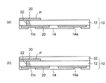
実施形態を説明する前に、基礎となる予備的事項について説明する。図1(a)に示すように、予備的事項に係る光導波路装置では、配線層200を備えた配線基板100の上に光導波路300が配置されている。光導波路300はコア層340が第1クラッド層320及び第2クラッド層360で囲まれた構造を有する。
Prior to describing the embodiment, preliminary items that serve as a basis will be described. As shown in FIG. 1A, in the optical waveguide device according to the preliminary matter, the
コア層340の端部には光路変換ミラーMが設けられている。また、第1クラッド層320及び第2クラッド層360には、配線層200の接続パッドPに到達するコンタクトホールCHが形成されている。
An optical path conversion mirror M is provided at the end of the
そして、図1(b)に示すように、光素子として、発光素子400を用意する。発光素子400は下側に接続端子420と発光部440とを備えている。発光素子400の発光部440は、本体の下面から下側に突出して形成されている。発光素子400の発光部440の突出する高さは2μm〜5μm程度である。
And as shown in FIG.1 (b), the
そして、発光素子400の接続端子420を配線基板100のコンタクトホールCH内に配置し、はんだ460を介して配線層200の接続パッドPに接続する。これにより、発光素子400の発光部440が光導波路300の光路変換ミラーMに光結合される。
Then, the
発光素子400の接続端子420の高さは、発光素子400を搭載する際に、発光素子400の本体の下面が第2クラッド層360の上面に接触する程度の高さに設定されている。
The height of the
このとき、発光素子400の発光部440は本体の下面から突出しているため、発光素子400の発光部440が第2クラッド層360を下側に押し込んだ状態となる。このため、第2クラッド層360とその下の光路変換ミラーMとが変形し、光路変換ミラーMの傾斜角度がずれてしまうことがある。
At this time, since the
その結果、発光素子400と光路変換ミラーMとの光結合の特性が劣化し、高い信頼性を得られなくなる課題がある。
As a result, there is a problem that the characteristics of optical coupling between the
また、リフロー加熱して発光素子400を搭載する際に、加熱された発光素子400の発光部440が第2クラッド層360に接触した状態で光路変換ミラーMにより近づくため、熱の影響によって光路変換ミラーMの光反射特性が劣化する懸念がある。
Further, when the
受光素子を搭載する場合においても、受光素子の受光部が本体の下面から突出しているため、同様な不具合が生じる。 Even when the light receiving element is mounted, the same problem occurs because the light receiving portion of the light receiving element protrudes from the lower surface of the main body.
以下に説明する実施形態では、前述した不具合を解消することができる。 In the embodiment described below, the above-described problems can be solved.
(実施形態)
図2〜図10は実施形態の光導波路装置の製造方法を示す図、図11は実施形態の光導波路装置を示す図である。以下、光導波路装置の製造方法を説明しながら、光導波路装置の構造を説明する。
(Embodiment)
2 to 10 are diagrams illustrating a method of manufacturing the optical waveguide device of the embodiment, and FIG. 11 is a diagram illustrating the optical waveguide device of the embodiment. Hereinafter, the structure of the optical waveguide device will be described while explaining the method for manufacturing the optical waveguide device.
実施形態の光導波路装置の製造方法では、まず、図2(a)に示すような配線基板10を用意する。配線基板10では、基板12の両面に配線層20がそれぞれ形成されている。
In the method of manufacturing an optical waveguide device according to the embodiment, first, a
基板12には厚み方向に貫通するスルーホールTHが設けられており、スルーホールTH内に貫通電極22が充填されている。両面側の配線層20は貫通電極22を介して相互接続されている。基板12の上面側の配線層20は、その一端に接続パッドPを備えている。
The
また、基板12の下面側に、配線層20の接続部上に開口部14aが設けられたソルダレジスト層14が形成されている。
Also, a solder resist
なお、スルーホールTHの側壁に形成されたスルーホールめっき層を介して両面側の配線層20が相互接続され、スルーホールTHの残りの孔に樹脂が充填されていてもよい。 Note that the wiring layers 20 on both sides may be interconnected via a through-hole plating layer formed on the side wall of the through-hole TH, and the remaining holes of the through-hole TH may be filled with resin.
また、基板12はリジット基板であってもよいし、あるいはフレキシブル基板でもよい。リジット基板とする場合は、基板12は例えばガラスエポキシ樹脂などから形成される。
The
あるいは、フレキシブル基板とする場合は、基板12は例えばポリイミドフィルムなどから形成される。また、基板12の両面側において、配線層20の積層数は任意に設定することができる。
Or when setting it as a flexible substrate, the board |
配線基板10のスルーホールTHはドリルやレーザなどで形成され、両面側の配線層20及び貫通電極22はフォトリソグラフィ及びめっき技術などを使用して形成される。
The through hole TH of the
次いで、図2(b)に示すように、配線基板10上の光導波路形成領域に、第1クラッド層を得るための感光性樹脂層(不図示)を形成し、フォトリソグラフィに基づいて露光/現像を行う。
Next, as shown in FIG. 2B, a photosensitive resin layer (not shown) for obtaining the first cladding layer is formed in the optical waveguide formation region on the
その後に、感光性樹脂層を100℃〜140℃程度の加熱処理によって硬化させる。これにより、配線基板10上の光導波路形成領域に第1クラッド層32が形成される。第1クラッド層32の厚みは、例えば10μm〜30μm程度である。
Thereafter, the photosensitive resin layer is cured by heat treatment at about 100 ° C to 140 ° C. As a result, the
感光性樹脂層としては、UV硬化型エポキシ樹脂などが好適に使用される。感光性樹脂層の形成方法としては、半硬化状態(B−ステージ)の感光性樹脂シートを貼付してもよいし、あるいは、液状の感光性樹脂を塗布してもよい。 As the photosensitive resin layer, a UV curable epoxy resin or the like is preferably used. As a method for forming the photosensitive resin layer, a semi-cured (B-stage) photosensitive resin sheet may be applied, or a liquid photosensitive resin may be applied.
後述するコア層及び第2クラッド層を形成する工程においても同様な樹脂が好適に使用される。 The same resin is preferably used also in the step of forming the core layer and the second cladding layer described later.
続いて、図3(a)に示すように、第1クラッド層32の上にコア層を得るための感光性樹脂層(不図示)を形成する。さらに、フォトリソグラフィに基づいて露光/現像を行った後に、感光性樹脂層を100℃〜140℃程度の加熱処理によって硬化させる。これにより、第1クラッド層32の上にコア層34が形成される。
Subsequently, as shown in FIG. 3A, a photosensitive resin layer (not shown) for obtaining a core layer is formed on the
このとき、図3(b)の平面図に示すように、第1クラッド層32の上にコア層34が複数の帯状パターンとして並んで形成される。コア層34の幅は30μm〜40μm程度に設定され、コア層34の厚みは30μm〜80μm程度に設定される。
At this time, as shown in the plan view of FIG. 3B, the
図3(a)は、図3(b)の平面図のI―Iの破線に沿った断面に相当する。後述する図4〜図5においても同じである。 FIG. 3A corresponds to a cross section taken along a broken line II in the plan view of FIG. The same applies to FIGS. 4 to 5 described later.
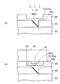
次いで、図4(a)及び(b)に示すように、コア層34の両端側の光路変換ミラーが配置される部分を切削装置の回転ブレードによって厚み方向に切削する。図4(a)及び(b)では、コア層34の一端側の領域が部分的に示されている。
Next, as shown in FIGS. 4A and 4B, the portion where the optical path conversion mirrors on both ends of the
これにより、光路を90°変換するための光路変換傾斜面Sを備えたV字状の分断部34aを形成する。光路変換傾斜面Sは、配線基板10の表面に対して好適には45°で傾斜して形成される。切削以外にも、レーザなどによって光路変換傾斜面Sを備えた分断部34aを形成することができる。
Thereby, the V-shaped
また、分断部34aは、コア層34を分断するように形成されていればよく、第1クラッド層32の厚みの途中まで形成されてもよい。
Moreover, the
次いで、図5(a)及び(b)に示すように、マスク蒸着などにより、コア層34の分断部34aの光路変換傾斜面Sに光反射性の金属層を部分的に形成して光路変換ミラーMを得る。光反射性の金属として、金又はアルミニウムなどがある。
Next, as shown in FIGS. 5A and 5B, a light-reflective metal layer is partially formed on the optical path conversion inclined surface S of the dividing
次に、図6(a)〜(c)を参照して、第1クラッド層32及びコア層34の上に、第2クラッド層36をパターニングする方法について説明する。図6(a)は図6(c)の平面図のII―IIの破線に沿った断面に相当する。また、図6(b)は図6(c)の平面図のIII―IIIの破線に沿った断面に相当する。
Next, a method for patterning the
後述する図7においても同じである。また、図6(c)の平面図は透視的に描かれており、後の平面図においても同じである。 The same applies to FIG. 7 described later. Further, the plan view of FIG. 6C is drawn in perspective, and the same applies to the subsequent plan views.
図6(a)に示すように、第1クラッド層32及びコア層34の上に、第2クラッド層を得るための感光性樹脂層(不図示)を形成する。さらに、フォトリソグラフィに基づいて露光/現像を行った後に、感光性樹脂層を100℃〜140℃程度の加熱処理によって硬化させる。
As shown in FIG. 6A, a photosensitive resin layer (not shown) for obtaining the second cladding layer is formed on the
これにより、第1クラッド層32の上に、コア層34を被覆する第2クラッド層36が形成される。第2クラッド層36の厚みは、例えば10μm〜30μm程度である。
As a result, a
このとき、図6(a)に図6(c)を加えて参照すると、第2クラッド層36は、所要部に開口部37が配置されてパターニングされる。第2クラッド層36の開口部37は、楕円状の第1開口部37aと、第1開口部37aの両端にそれぞれ繋がる細長四角状の第2開口部37bとから形成される。
At this time, referring to FIG. 6A in addition to FIG. 6C, the
第2クラッド層36の第1開口部37aは、コア層34に形成された光路変換ミラーMを含む領域の上に配置される。第2クラッド層36の第1開口部37aは、後述するように、光素子として発光素子を搭載する際に、発光素子の突出する発光部が第2クラッド層36に当たらないようにするために形成される。
The
このため、第2クラッド層36の第1開口部37aの面積は発光素子の発光部の面積より一回り大きく設定される。また、第1開口部37aのコア層34の上面まで深さは、発光素子の発光部の突出高さよりも深く形成される。
Therefore, the area of the
また、第1開口部37aの両端に繋がる2つの第2開口部37bは、配線基板10の接続パッドPを含む領域の上にそれぞれ配置される。第2クラッド層36の第2開口部37bは、接続パッドPの少なくとも一部を含む領域に配置されていればよい。
In addition, the two
第2クラッド層36の第2開口部37bは、後述するように、コンタクトホール内の接続パッドPに発光素子の接続端子を接続した後に、コンタクトホール内にアンダーフィル樹脂を流し込むための流路として機能する。
As described later, the
このため、第2クラッド層36の第2開口部37bは、接続パッドP上に配置されるコンタクトホールに連通するように配置される。
Therefore, the
また、第2クラッド層36の第2開口部37bの長さは搭載される発光素子の幅よりも長く設定され、発光素子が搭載される際にその外側に第2クラッド層36の第2開口部37bの一部が露出するようにする。
The length of the
図6(c)の平面図の例では、配線層20の接続パッドPの直径が第2クラッド層36の第2開口部37bの幅よりも大きく設定されている。例えば、配線層20の接続パッドPの直径は60μm〜80μmであり、第2クラッド層36の第2開口部37bの幅が30μm〜40μm程度である。
In the example of the plan view of FIG. 6C, the diameter of the connection pad P of the
このため、図6(c)の平面図の例では、第2クラッド層36の第2開口部37bは、接続パッドPの一部が第2開口部37bの側壁から外側にはみ出すようにして接続パッドPの上に配置される。
Therefore, in the example of the plan view of FIG. 6C, the
あるいは、接続パッドPの直径を第2クラッド層36の第2開口部37bの幅よりも小さくして、第2クラッド層36の第2開口部37b内に接続パッドPの全体が配置されるようにしてもよい。
Alternatively, the diameter of the connection pad P is made smaller than the width of the
次いで、図7(a)〜(c)に示すように、レーザにより第2クラッド層36及び第1クラッド層32を加工することにより、配線基板10の配線層20の接続パッドPに到達するコンタクトホールCHを形成する。
Next, as shown in FIGS. 7A to 7C, the contact reaching the connection pad P of the
図7(c)に示すように、コンタクトホールCHは、第2クラッド層36の第2開口部37bの側壁から外側にはみ出した状態で、接続パッドP上に配置される。コンタクトホールCHは第2クラッド層36の第2開口部37bに連通して形成される。
As shown in FIG. 7C, the contact hole CH is disposed on the connection pad P in a state of protruding outward from the side wall of the
これにより、図7(a)に示すように、配線基板10の上に、下から順に、第1クラッド層32、コア層34及び第2クラッド層が形成された光導波路30が得られる。
As a result, as shown in FIG. 7A, the
なお、前述した図6〜図7の製造方法では、フォトリソグラフィに基づいて第2クラッド層36に開口部37を形成した後に、レーザで第2クラッド層36及び第1クラッド層32を開口してコンタクトホールCHを形成している。
6 to 7 described above, after the
この製造方法の他に、図8(a)に示すように、前述した図2(b)の工程で、第1クラッド層32にフォトリソグラフィによりコンタクトホールCHを同時に形成してもよい。あるいは、前述した図2(b)の工程の後に、レーザで第1クラッド層32にコンタクトホールCHを形成してもよい。
In addition to this manufacturing method, as shown in FIG. 8A, the contact hole CH may be simultaneously formed in the
その後に、図8(b)に示すように、前述した図6(b)の工程で、コンタクトホールCHに連通するように、第2クラッド層36に第1、第2開口部37a,37bを形成する。これにより、図7(a)及び(b)と同一構造の光導波路30を得ることができる。
Thereafter, as shown in FIG. 8B, the first and
この方法では、コンタクトホールCHの領域上の第2クラッド層36の第2開口部37bは、コンタクトホールCHの側壁となるように半円状に外側に突出して形成される。
In this method, the
次に、図9(a)〜(c)を参照して、上記した図7(a)〜(c)の構造体に光素子を搭載する方法について説明する。光素子としては、発光素子又は受光素子が使用されるが、発光素子を例に挙げて説明する。 Next, with reference to FIGS. 9A to 9C, a method of mounting an optical element on the structure shown in FIGS. 7A to 7C will be described. As the optical element, a light-emitting element or a light-receiving element is used. The light-emitting element will be described as an example.
前述した図6と同様に、図9(a)は図9(c)の平面図のIV―IVの破線に沿った断面に相当する。図9(b)は図9(c)の平面図のV―Vの破線に沿った断面に相当する。後述する図10及び図11においても同じである。また、図9(c)は透視的に描かれている。 Like FIG. 6 described above, FIG. 9A corresponds to a cross section taken along the broken line IV-IV in the plan view of FIG. 9C. FIG. 9B corresponds to a cross section taken along the broken line VV in the plan view of FIG. The same applies to FIGS. 10 and 11 described later. Further, FIG. 9C is drawn in perspective.
図9(a)及び(b)に示すように、下面に接続端子42と発光部44とを備えた発光素子40を用意する。接続端子42は金バンプなどのバンプ電極から形成される。また、発光部44は発光素子40の本体の下面から下側に突出して形成される。発光素子40の発光部44の突出する高さは2μm〜5μm程度である。
As shown in FIGS. 9A and 9B, a
そして、発光素子40の接続端子42をコンタクトホールCH内の接続パッドPに配置し、リフロー加熱を行ってはんだ44により接続する。
Then, the
これにより、発光素子40の発光部44がコア層34の光路変換ミラーMに光結合される。
As a result, the
このとき、発光素子40の発光部44の下の第2クラッド層36に第1開口部37aが配置されているため、発光素子40の突出する発光部44は第2クラッド層36の第1開口部37aに収容される。これにより、発光素子40の発光部44が第2クラッド層36を下側に押し込んで光路変換ミラーMが変形する不具合が解消される。
At this time, since the
また、発光素子40の発光部44は本体から突出する高さ分だけ、光路変換ミラーMとの距離が近くなるため、光学特性を向上させることができる。
Further, since the
さらには、リフロー加熱を行って発光素子40を接続パッドPに接続する際に、加熱された発光素子40の発光部44が第2クラッド層36に接触しなくなる。このため、発光素子40からの熱の影響による光路変換ミラーMの劣化が防止される。
Furthermore, when the
またこのとき、図9(c)の平面図を参照すると、前述したように、コンタクトホールCHに連通する第2クラッド層36の第2開口部37bの長さは、発光素子40の幅よりも長く設定されている。このため、発光素子40を搭載すると、発光素子40の外側に第2クラッド層36の第2開口部37bの両端側の一部がそれぞれ露出した状態となる。
At this time, referring to the plan view of FIG. 9C, as described above, the length of the
このように、発光素子40の少なくとも一端が第2クラッド層36の第2開口部37bの内側に配置されるようにする。
In this manner, at least one end of the
また、発光素子40の接続端子42の高さは、コンタクトホールCHの底の接続パッドPの表面から第2クラッド層36の第2開口部37bの上端までの高さよりも低く設定されている。このため、図9(a)に示すように、発光素子40の発光部44を除く下面が第2クラッド層36の上面に当接して、発光素子40の高さ位置が決められて最適な平行度が確保される。
The height of the
このように、発光素子40の下面が第2クラッド層36の上面に接した状態で、発光素子40の外側にアンダーフィル樹脂の流路となる第2クラッド層36の第2開口部37bが露出して配置される。
As described above, the
次いで、図10(a)及び(b)に示すように、ディスペンサなどによって発光素子40の側面近傍に液状のアンダーフィル樹脂を一括して塗布する。このとき、アンダーフィル樹脂は、毛細管現象により第2クラッド層36の第2開口部37bが流路となって第2開口部37bに連通する第1開口部37a及びコンタクトホールCH内まで浸透していく。
Next, as shown in FIGS. 10A and 10B, a liquid underfill resin is collectively applied to the vicinity of the side surface of the
これにより、図11(a)〜(c)に示すように、発光素子40の下側の第2クラッド層36の第1開口部37a及び第2開口部37bと、それに連通するコンタクトホールCHの側面と発光素子40の接続端子42との隙間にアンダーフィル樹脂50が充填される。
Accordingly, as shown in FIGS. 11A to 11C, the
以上により、第2クラッド層36の第1開口部37a内の光路変換ミラーMがアンダーフィル樹脂50によって封止される。
As described above, the optical path conversion mirror M in the
図11(c)の平面図では、アンダーフィル樹脂50は斜線ハッチングされた領域に充填される。また、図11(a)に示すように、発光素子40が第2クラッド層36と接している部分では、発光素子40の両外側にアンダーフィル樹脂50が残された状態となる。
In the plan view of FIG. 11C, the
このようにして、本実施形態では、発光素子40の下面が第2クラッド層36の上面に接して搭載されるとしても、発光素子40の外側に、コンタクトホールCHに連通する第2クラッド層36の第2開口部37bの一部が露出するようにしている。
Thus, in the present embodiment, even if the lower surface of the
このため、第2クラッド層36の第2開口部37bから発光素子40の下側のコンタクトホールCHにアンダーフィル樹脂50を容易に充填することができる。
Therefore, the
以上により、図11(a)〜(c)に示すように、実施形態の光導波路装置1が得られる。
By the above, as shown to Fig.11 (a)-(c), the
図11(a)及び(b)に示すように、実施形態の光導波路装置1は、前述した図2(a)で説明した配線基板10を備えている。配線基板10の上には光導波路30が形成されている。
As shown in FIGS. 11A and 11B, the
光導波路30は、第1クラッド層32と、その上に形成されたコア層34と、それを被覆する第2クラッド層36とから形成され、コア層34が第1、第2クラッド層32,36で囲まれた構造を有する。コア層34の屈折率は、第1クラッド層32及び第2クラッド層36の屈折率よりも高くなるように設定されている。
The
また、光導波路30のコア層34の端部には光反射性の金属から形成された光路変換ミラーMが配置されている。
An optical path conversion mirror M made of a light reflective metal is disposed at the end of the
図11(b)及び(c)に示すように、第2クラッド層36及び第1クラッド層32には配線層20の接続パッドPに到達するコンタクトホールCHが形成されている。さらに、第2クラッド層36には開口部37が形成されている。
As shown in FIGS. 11B and 11C, contact holes CH reaching the connection pads P of the
第2クラッド層36の開口部37は、光導波路30の光路変換ミラーMを含む領域上に配置された第1開口部37aと、その両端に繋がった第2開口部37bとから形成される。
The
第2クラッド層36の第2開口部37bは、接続パッドPを含む領域に形成され、コンタクトホールCHに連通している。また、第2クラッド層36の第2開口部37bは、コア層34の延在方向と同一方向に延びる細長四角状で形成されている。
The
また、発光素子40の接続端子42がコンタクトホールCHに配置され、はんだ46を介して配線層20の接続パッドPに接続されている。発光素子40は、その下面に下側に突出して形成された発光部44を備えている。
Further, the
第2クラッド層36の第1開口部37aの面積は、発光素子40の発光部44の面積よりも大きく設定されている。また、第2クラッド層36の第1開口部37aの深さは、発光素子40の発光部44の突出高さよりも深く設定されている。
The area of the
そして、発光素子40の突出する発光部44が第2クラッド層36の第1開口部37aに収容され、第2クラッド層36に接触していない。
The protruding
第2クラッド層36の第2開口部37bの長さは、発光素子40の幅よりも長く設定されている。これにより、発光素子40の両外側に第2クラッド層36の第2開口部37bの一部がはみ出して露出している。
The length of the
このように、発光素子40の少なくとも一端が第2クラッド層36の第2開口部37bの内側に配置されるようにする。
In this manner, at least one end of the
また、発光素子40の接続端子42の高さは、コンタクトホールCHの底の接続パッドPの表面から第2クラッド層36の第2開口部37bの上端までの高さよりも低く設定されている。このため、発光素子40の下面は第2クラッド層36の上面に接して、発光素子40の高さ位置が決められて最適な平行度が確保されている。
The height of the
さらに、図11(b)及び(c)に示すように、第2クラッド層36の第1開口部37a、第2開口部37b、及びコンタクトホールCHの側壁と発光素子40の接続端子42との隙間に、発光素子40の下側を封止するアンダーフィル樹脂50が充填されている。
Further, as shown in FIGS. 11B and 11C, the
発光素子40としては、面発光レーザ(VCSEL:Vertical Cavity Surface Emitting Laser)が好適に使用される。また、光素子として、受光素子を使用する場合は、フォトダイオードが好適に使用される。
As the
そして、発光素子40の発光部44が光路変換ミラーMと光結合される。あるいは、光素子として、受光素子を使用する場合は、受光素子の下面に突出して形成された受光部が光路変換ミラーMと光結合される。
Then, the
前述したように、実施形態の光導波路装置1では、発光素子40の突出する発光部44は第2クラッド層36の第1開口部37aに収容される。このため、発光素子40の発光部44が第2クラッド層36を押し込んで光路変換ミラーMが変形する不具合が解消される。
As described above, in the
これにより、発光素子40と光路変換ミラーMとの光結合の高い信頼性を確保することができる。
Thereby, high reliability of light coupling between the light emitting
また、発光素子40の発光部44は本体から突出する高さ分だけ、光路変換ミラーMとの距離が近くなるため、光学特性を向上させることができる。
Further, since the
さらには、リフロー加熱を行って発光素子40を接続パッドPに接続する際に、加熱された発光素子40の発光部44が第2クラッド層36に接触しないため、発光素子40からの熱の影響による光路変換ミラーMの劣化が防止される。
Furthermore, when the light-emitting
また、アンダーフィル樹脂50は発光素子40の外側に配置された第2クラッド層36の第2開口部37bが流路となってコンタクトホールCH内に充填される。
The
各コンタクトホールCHが第2クラッド層36の第2開口部37bに連通しているため、全てのコンタクトホールCHにアンダーフィル樹脂50を信頼性よく充填することができる。
Since each contact hole CH communicates with the
これにより、後に加熱処理が行われるとしても、コンタクトホールCH内で空気が膨張することがなく、発光素子40と配線基板10の接続パッドPとの電気的な接続の信頼性を確保することができる。
Thereby, even if heat treatment is performed later, the air does not expand in the contact hole CH, and the reliability of the electrical connection between the light emitting
また、発光素子40を搭載する際に、光導波路30の上面に発光素子40の下面を当接させるため、高さや平行度を容易に最適化することができ、光学特性を向上させることができる。
Further, since the lower surface of the
図12には、図11(a)の発光素子40に制御素子60が接続された様子が示されている。図12に示すように、発光素子40の横方向の配線基板10の上には、配線層20の接続部上に開口部15aが設けられたソルダレジスト層15が形成されている。
FIG. 12 shows a state in which the
そして、制御素子60の接続端子62が配線層20の接続部にはんだ64を介して接続されている。さらに、制御素子60の下側にアンダーフィル樹脂50aが充填されている。
The
このようにして、発光素子40は配線基板10の配線層20を介して制御素子60に電気的に接続されている。
In this way, the
次に、図11及び図12を参照して、実施形態の光導波路装置1の光伝搬について説明する。図12において、光素子として、発光素子40が使用される場合は、制御素子60がドライバ素子として配置される。そして、ドライバ素子から出力される電気信号が発光素子に供給され、発光素子の発光面から下側に光が出射される。
Next, with reference to FIG.11 and FIG.12, the light propagation of the
発光素子40から出射される光は、アンダーフィル樹脂50を透過して光路変換ミラーM(図11(a))に到達する。さらに、光路変換ミラーMで光が反射され、光路が90°変換されてコア層34に入射する。
Light emitted from the
次いで、コア層34に入射した光は、コア層34内で全反射を繰り返して伝播し、他端側の光路変換ミラーMで光路が90°変換されて受光素子の受光部に入射する。
Next, the light incident on the
逆に、光素子として、受光素子が使用される場合は、制御素子60がアンプ素子として配置される。この場合は、上記した光経路と逆方向に光伝搬され、受光素子の受光部に光が入射される。さらに、受光素子は光信号を電気信号に変換し、アンプ素子に電気信号が供給される。
Conversely, when a light receiving element is used as the optical element, the
(その他の実施形態)
図13及び図14は、前述した図7の第2クラッド層36の第1開口部37a及び第2開口部37bの変形例を示す平面図である。前述した図7では、第2クラッド層36の第1開口部37aの両端に繋がる2つの第2開口部37bは、他の第2開口部37bと相互に分離されて配置されている。
(Other embodiments)
13 and 14 are plan views showing modifications of the
図13の第1の変形例に示すように、図7の第2クラッド層36の各第2開口部37bの一端を縦方向に配置される共通開口部37xで繋ぐことにより、全ての第1開口部37a、全ての第2開口部37b、及び全てのコンタクトホールCHが連通するようにしてもよい。
As shown in the first modification of FIG. 13, one end of each
また、図14の第2の変形例のように、第1開口部37aの両端に繋がる2つ第2開口部37bが、2つのコンタクトホールCHを含む領域に一括して配置された第3開口部37cに繋がっていてもよい。この場合は、2つのコンタクトホールCHの全体が一つの第2クラッド層36の第3開口部37cに配置され、コンタクトホールCHは第1クラッド層32のみに形成される。
Further, as in the second modification of FIG. 14, the third opening in which two
このように、第2クラッド層36の第1開口部37a及び第2開口部37bは、光導波路30に干渉しないように、光路変換ミラーMを含む領域に配置されてコンタクトホールCHに連通していればよく、各種の形状を採用することができる。
As described above, the
第2クラッド層36の第2開口部37bがコンタクトホールCHに連通していることで、第2クラッド層36の第2開口部37bを流路としてアンダーフィル樹脂50を第1開口部37a及びコンタクトホールCHに充填することができる。
Since the
図15には、第2クラッド層の開口部の別の態様が示されている。図15に示すように、コンタクトホールCH内にアンダーフィル樹脂50を充填する必要がない場合は、第2クラッド層36の第1開口部37aに繋がってコンタクトホールCHに連通する第2開口部37bを省略してもよい。
FIG. 15 shows another aspect of the opening of the second cladding layer. As shown in FIG. 15, when there is no need to fill the contact hole CH with the
この態様の場合は、第2クラッド層36に形成される開口部37は、コア層34の光路変換ミラーMを含む領域上に配置される楕円状の第1開口部37aと、第1開口部37aに繋がってコア層34の延在方向に延びる長方形状の第4開口部37dとによって形成される。
In the case of this aspect, the
そして、同様に発光素子40が搭載され、第2クラッド層36の第4開口部37dの一部が発光素子40から露出する。さらに、露出した部分の第4開口部37dから第1開口部37aにアンダーフィル樹脂が充填される。
Similarly, the
また、この態様の場合であっても、コンタクトホールCH内に予め先入れ用の樹脂を塗布しておき、発光素子の接続端子を樹脂を介して接続パッドに接続することで、コンタクトホールCH内にも樹脂を充填することも可能である。 Even in the case of this aspect, a resin for pre-filling is applied in advance in the contact hole CH, and the connection terminal of the light emitting element is connected to the connection pad through the resin, so that the inside of the contact hole CH It is also possible to fill the resin.
(その他の製造方法)
前述した図6(a)〜(c)の工程では、フォトリソグラフィに基づいて第2クラッド層36に開口部37を形成している。この方法の他に、図16(a)に示すように、非感光性樹脂から第2クラッド層36を形成し、レーザによって凹状の開口部37を形成してもよい。
(Other manufacturing methods)
6A to 6C described above, an
この場合、第2クラッド層36の複数の開口部37に対応する開口部が設けられたマスクを介して面発光レーザによって一括してレーザ照射される。これにより、レーザ加工によって複数の開口部37を一括して形成することができる。
In this case, laser irradiation is performed collectively by a surface emitting laser through a mask provided with openings corresponding to the plurality of
図16(a)に示すように、レーザによって第2クラッド層36に開口部37を形成する場合は、第2クラッド層36の厚みの途中まで凹状の開口部37が形成される。第2クラッド層36の開口部37の深さは、発光素子40の発光部44の突出高さよりも深く形成される。
As shown in FIG. 16A, when the
コア層34の分断部34a内に第2クラッド層36が残され、光路変換ミラーMが第2クラッド層36で被覆された状態となる。
The
また、第2クラッド層36の開口部37の底部において、コア層34の上に薄膜の第2クラッド層36が残される。
The thin
そして、図16(b)に示すように、前述した図9(a)〜図11(c)の工程と同様に、第2クラッド層36の上に発光素子40を搭載した後に、第2クラッド層36の開口部37にアンダーフィル樹脂50を充填する。
As shown in FIG. 16B, after the
図16(b)の構造では、光導波路30の光路変換ミラーMが第2クラッド層36で保護されてアンダーフィル樹脂50と接触しないため、信頼性の面で有利になる。
In the structure of FIG. 16B, the optical path conversion mirror M of the
1…光導波路装置、10…配線基板、12…基板、14,15…ソルダレジスト層、14a,15a…開口部、20…配線層、22…貫通電極、30…光導波路、32…第1クラッド層、34…コア層、34a…分断部、36…第2クラッド層、37a…第1開口部、37b…第2開口部、37c…第3開口部、37d…第4開口部、37x…共通開口部、40…発光素子、42,62…接続端子、44…発光部、50,50a…アンダーフィル樹脂、60…制御素子、CH…コンタクトホール、S…光路変換傾斜面、M…光路変換ミラー、TH…スルーホール。
DESCRIPTION OF
Claims (9)
前記配線基板の上面に形成された接続パッドと、
前記配線基板の上に、第1クラッド層、コア層及び第2クラッド層が順に形成された光導波路と、
前記コア層に形成された光路変換ミラーと、
前記接続パッドの上の前記第1クラッド層に形成されたコンタクトホールと、
前記第2クラッド層に形成され、前記光路変換ミラー上の領域に配置された第1開口部と、前記第1開口部に繋がって前記コンタクトホールに連通する第2開口部とを備えた開口部と、
前記第2クラッド層の上に、少なくとも一端が前記第2開口部の内側に配置され、前記第2開口部の一部が露出するように搭載された光素子と、
前記第2クラッド層の前記第1開口部内に配置され、前記光素子の下側に突出する発光部又は受光部と、
前記第2クラッド層の開口部に充填されたアンダーフィル樹脂と
を有し、
前記光素子の接続端子が前記コンタクトホール内の前記接続パッドに接続され、前記第2クラッド層の開口部及び前記コンタクトホールに前記アンダーフィル樹脂が充填されていることを特徴とする光導波路装置。 A wiring board;
Connection pads formed on the upper surface of the wiring board;
An optical waveguide in which a first cladding layer, a core layer, and a second cladding layer are sequentially formed on the wiring substrate;
An optical path conversion mirror formed in the core layer;
A contact hole formed in the first cladding layer on the connection pad;
An opening having a first opening formed in the second cladding layer and disposed in a region on the optical path conversion mirror, and a second opening connected to the first opening and communicating with the contact hole. When,
On the second cladding layer, and at least one end is disposed inside the second opening, a light element mounted so that to expose a portion of the second opening,
A light emitting part or a light receiving part disposed in the first opening of the second clad layer and projecting below the optical element;
An underfill resin filled in the opening of the second cladding layer,
An optical waveguide device, wherein a connection terminal of the optical element is connected to the connection pad in the contact hole, and the underfill resin is filled in the opening of the second cladding layer and the contact hole.
前記配線基板の上に、前記光素子に電気的に接続された制御素子を有することを特徴とする請求項1又は2に記載の光導波路装置。 The optical element is a light emitting element or a light receiving element,
The optical waveguide device according to claim 1, further comprising a control element electrically connected to the optical element on the wiring board.
前記開口部は複数の前記第2開口部に繋がる第3開口部を備えることを特徴とする請求項1乃至4のいずれか1項に記載の光導波路装置。5. The optical waveguide device according to claim 1, wherein the opening includes a third opening connected to the plurality of second openings. 6.
前記配線基板の上に第1クラッド層を形成する工程と、
前記第1クラッド層の上にコア層を形成する工程と、
前記コア層に光路変換ミラーを形成する工程と、
前記第1クラッド層及び前記コア層の上に第2クラッド層を形成する工程とを有し、
前記接続パッドの上の前記第1クラッド層にコンタクトホールが形成され、かつ、前記第2クラッド層に、前記光路変換ミラー上の領域に配置された第1開口部と、前記第1開口部に繋がって前記コンタクトホールに連通する第2開口部とを備えた開口部が形成された構造が得られ、
前記第2クラッド層を形成する工程の後に、
下側から突出する発光部又は受光部を備えた光素子を用意する工程と、
前記発光部又は受光部が前記第2クラッド層の前記第1開口部内に配置され、かつ前記光素子の少なくとも一端が前記第2開口部の内側に配置され、かつ前記第2開口部の一部が露出するように、前記第2クラッド層の上に前記光素子を搭載する工程と、
前記第2クラッド層の開口部にアンダーフィル樹脂を充填する工程と
を有し、
前記光素子の接続端子が前記コンタクトホール内の前記接続パッドに接続され、前記第2クラッド層の開口部及び前記コンタクトホールに前記アンダーフィル樹脂が充填されることを特徴とする光導波路装置の製造方法。 Preparing a wiring board having connection pads on the upper surface;
Forming a first cladding layer on the wiring substrate;
Forming a core layer on the first cladding layer;
Forming an optical path conversion mirror in the core layer;
Forming a second cladding layer on the first cladding layer and the core layer,
A contact hole is formed in the first cladding layer on the connection pad, and a first opening is disposed in the second cladding layer in a region on the optical path conversion mirror, and in the first opening. A structure in which an opening having a second opening connected to the contact hole is formed is obtained,
After the step of forming the second cladding layer,
Preparing an optical element having a light emitting part or a light receiving part protruding from the lower side;
The light emitting portion or the light receiving portion is disposed within said first opening of said second cladding layer, and at least one end is disposed inside the second opening, and a portion of the second opening portion of the optical element to but so that to expose the step of mounting the optical element on the second cladding layer,
Filling the opening of the second cladding layer with an underfill resin,
The optical waveguide device is manufactured by connecting a connection terminal of the optical element to the connection pad in the contact hole, and filling the opening of the second cladding layer and the contact hole with the underfill resin. Method.
前記開口部が前記光路変換ミラー上の領域から前記接続パッド上の領域まで繋がって形成され、
前記第2クラッド層を形成する工程の後に、
前記第2クラッド層の開口部に連通し、前記接続パッドに到達する前記コンタクトホールを前記第1クラッド層に形成する工程を有することを特徴とする請求項6に記載の光導波路装置の製造方法。 In the step of forming the second cladding layer,
The opening is formed from the region on the optical path conversion mirror to the region on the connection pad,
After the step of forming the second cladding layer,
7. The method of manufacturing an optical waveguide device according to claim 6 , further comprising a step of forming, in the first cladding layer, the contact hole that communicates with the opening of the second cladding layer and reaches the connection pad. .
前記光素子の発光部又は受光部を除く下面を前記第2クラッド層の上面に当接させることを特徴とする請求項6又は7に記載の光導波路装置の製造方法。 In the step of mounting the optical element,
The method of manufacturing the optical waveguide device according to claim 6 or 7, characterized in that is brought into contact with the upper surface of the light emitting portion or the lower surface excluding the light receiving portion before Symbol second cladding layer of the optical element.
前記配線基板の上に、前記光素子に電気的に接続される制御素子を搭載する工程を有することを特徴とする請求項6乃至8のいずれか一項に記載の光導波路装置の製造方法。
The optical element is a light emitting element or a light receiving element,
On the wiring board, method of manufacturing the optical waveguide device according to any one of claims 6 to 8, comprising a step of mounting a control element electrically connected to the optical element.
Priority Applications (2)
| Application Number | Priority Date | Filing Date | Title |
|---|---|---|---|
| JP2015086787A JP6437875B2 (en) | 2015-04-21 | 2015-04-21 | Optical waveguide device and manufacturing method thereof |
| US15/098,670 US9671575B2 (en) | 2015-04-21 | 2016-04-14 | Optical waveguide device and method of manufacturing the same |
Applications Claiming Priority (1)
| Application Number | Priority Date | Filing Date | Title |
|---|---|---|---|
| JP2015086787A JP6437875B2 (en) | 2015-04-21 | 2015-04-21 | Optical waveguide device and manufacturing method thereof |
Publications (3)
| Publication Number | Publication Date |
|---|---|
| JP2016206377A JP2016206377A (en) | 2016-12-08 |
| JP2016206377A5 JP2016206377A5 (en) | 2017-12-28 |
| JP6437875B2 true JP6437875B2 (en) | 2018-12-12 |
Family
ID=57147659
Family Applications (1)
| Application Number | Title | Priority Date | Filing Date |
|---|---|---|---|
| JP2015086787A Active JP6437875B2 (en) | 2015-04-21 | 2015-04-21 | Optical waveguide device and manufacturing method thereof |
Country Status (2)
| Country | Link |
|---|---|
| US (1) | US9671575B2 (en) |
| JP (1) | JP6437875B2 (en) |
Families Citing this family (10)
| Publication number | Priority date | Publication date | Assignee | Title |
|---|---|---|---|---|
| JP6461506B2 (en) * | 2014-07-31 | 2019-01-30 | 株式会社エンプラス | Optical receptacle and optical module |
| JP6461509B2 (en) * | 2014-08-04 | 2019-01-30 | 株式会社エンプラス | Optical receptacle and optical module |
| JP6492169B2 (en) | 2015-04-27 | 2019-03-27 | 京セラ株式会社 | Optical transmission board and optical transmission module |
| US9721812B2 (en) * | 2015-11-20 | 2017-08-01 | International Business Machines Corporation | Optical device with precoated underfill |
| US10018781B1 (en) * | 2017-01-06 | 2018-07-10 | International Business Machines Corporation | Fluid control structure |
| JP2018163186A (en) * | 2017-03-24 | 2018-10-18 | 京セラ株式会社 | Optical circuit board |
| JP6941460B2 (en) * | 2017-03-31 | 2021-09-29 | 日東電工株式会社 | Photoelectric mixed board and photo-electric mixed board assembly |
| JP2019029389A (en) * | 2017-07-26 | 2019-02-21 | 京セラ株式会社 | Optical circuit board |
| US20220413212A1 (en) * | 2019-11-28 | 2022-12-29 | Kyocera Corporation | Optical element mounting module |
| JP7358224B2 (en) * | 2019-12-09 | 2023-10-10 | 新光電気工業株式会社 | Optical module and its manufacturing method |
Family Cites Families (9)
| Publication number | Priority date | Publication date | Assignee | Title |
|---|---|---|---|---|
| AU7885900A (en) * | 1999-08-27 | 2001-03-26 | Board Of Regents, The University Of Texas System | Packaging enhanced board level opto-electronic interconnects |
| JP3991220B2 (en) | 2001-02-28 | 2007-10-17 | 日本電気株式会社 | Method for manufacturing optical circuit element |
| EP1286194A3 (en) * | 2001-08-21 | 2004-05-19 | Canon Kabushiki Kaisha | Optical waveguide apparatus |
| SE525405C2 (en) * | 2002-08-09 | 2005-02-15 | Acreo Ab | Mirrors for polymeric guides, process for their preparation, and optical waveguide device |
| JP2013186310A (en) * | 2012-03-08 | 2013-09-19 | Shinko Electric Ind Co Ltd | Photoelectric composite substrate and method for manufacturing the same |
| JP5989412B2 (en) * | 2012-06-11 | 2016-09-07 | 新光電気工業株式会社 | Optical module and optical module manufacturing method |
| JP6105254B2 (en) | 2012-10-29 | 2017-03-29 | 新光電気工業株式会社 | Optical waveguide laminated wiring board, optical module, and optical waveguide laminated wiring board manufacturing method |
| US9354408B2 (en) * | 2012-11-22 | 2016-05-31 | International Business Machines Corporation | Via for electrical contact passing through layers of optical waveguide in multilayer structure including electrical substrate and laminated layers of optical waveguide |
| JP6235878B2 (en) * | 2013-11-25 | 2017-11-22 | 新光電気工業株式会社 | Optical waveguide device and manufacturing method thereof |
-
2015
- 2015-04-21 JP JP2015086787A patent/JP6437875B2/en active Active
-
2016
- 2016-04-14 US US15/098,670 patent/US9671575B2/en active Active
Also Published As
| Publication number | Publication date |
|---|---|
| JP2016206377A (en) | 2016-12-08 |
| US9671575B2 (en) | 2017-06-06 |
| US20160313517A1 (en) | 2016-10-27 |
Similar Documents
| Publication | Publication Date | Title |
|---|---|---|
| JP6437875B2 (en) | Optical waveguide device and manufacturing method thereof | |
| JP4260650B2 (en) | Photoelectric composite substrate and manufacturing method thereof | |
| US9081159B2 (en) | Optical waveguide and method of manufacturing the same, and optical waveguide device | |
| JP4690870B2 (en) | Opto-electric integrated wiring board and opto-electric integrated wiring system | |
| US20080044127A1 (en) | Printed Circuit Board Element Comprising at Least One Optical Waveguide, and Method for the Production of Such a Printed Circuit Board Element | |
| JP5395734B2 (en) | Method for manufacturing photoelectric composite substrate | |
| JP5313849B2 (en) | Optical waveguide device and manufacturing method thereof | |
| JP2009175418A (en) | Opto-electronic printed wiring board and manufacturing method of same | |
| JP5479310B2 (en) | Optical waveguide, manufacturing method thereof, and optical waveguide device | |
| JP6235878B2 (en) | Optical waveguide device and manufacturing method thereof | |
| JP2008139465A (en) | Method of manufacturing optoelectric hybrid board | |
| US11378763B2 (en) | Optical waveguide having support member, optical waveguide mounting substrate and optical transceiver | |
| JP6084027B2 (en) | Optical waveguide device and manufacturing method thereof | |
| JP6637368B2 (en) | Optical waveguide device and method of manufacturing the same | |
| JP6435111B2 (en) | Optical waveguide device and manufacturing method thereof | |
| JP5976769B2 (en) | Optical waveguide and optical waveguide device | |
| JP6084024B2 (en) | Optical waveguide device and manufacturing method thereof | |
| JP4698728B2 (en) | Opto-electric integrated wiring board and opto-electric integrated wiring system | |
| JP7280031B2 (en) | Optical waveguide mounting substrate, optical communication device, and method for manufacturing optical waveguide mounting substrate | |
| JP4691196B2 (en) | Opto-electric integrated wiring board and opto-electric integrated wiring system |
Legal Events
| Date | Code | Title | Description |
|---|---|---|---|
| A521 | Request for written amendment filed |
Free format text: JAPANESE INTERMEDIATE CODE: A523 Effective date: 20171115 |
|
| A621 | Written request for application examination |
Free format text: JAPANESE INTERMEDIATE CODE: A621 Effective date: 20171115 |
|
| RD03 | Notification of appointment of power of attorney |
Free format text: JAPANESE INTERMEDIATE CODE: A7423 Effective date: 20180207 |
|
| RD04 | Notification of resignation of power of attorney |
Free format text: JAPANESE INTERMEDIATE CODE: A7424 Effective date: 20180215 |
|
| A977 | Report on retrieval |
Free format text: JAPANESE INTERMEDIATE CODE: A971007 Effective date: 20180620 |
|
| A131 | Notification of reasons for refusal |
Free format text: JAPANESE INTERMEDIATE CODE: A131 Effective date: 20180807 |
|
| A521 | Request for written amendment filed |
Free format text: JAPANESE INTERMEDIATE CODE: A523 Effective date: 20180928 |
|
| TRDD | Decision of grant or rejection written | ||
| A01 | Written decision to grant a patent or to grant a registration (utility model) |
Free format text: JAPANESE INTERMEDIATE CODE: A01 Effective date: 20181106 |
|
| A61 | First payment of annual fees (during grant procedure) |
Free format text: JAPANESE INTERMEDIATE CODE: A61 Effective date: 20181115 |
|
| R150 | Certificate of patent or registration of utility model |
Ref document number: 6437875 Country of ref document: JP Free format text: JAPANESE INTERMEDIATE CODE: R150 |