JP6084027B2 - Optical waveguide device and manufacturing method thereof - Google Patents
Optical waveguide device and manufacturing method thereof Download PDFInfo
- Publication number
- JP6084027B2 JP6084027B2 JP2012277550A JP2012277550A JP6084027B2 JP 6084027 B2 JP6084027 B2 JP 6084027B2 JP 2012277550 A JP2012277550 A JP 2012277550A JP 2012277550 A JP2012277550 A JP 2012277550A JP 6084027 B2 JP6084027 B2 JP 6084027B2
- Authority
- JP
- Japan
- Prior art keywords
- optical
- wiring layer
- layer
- optical waveguide
- substrate
- Prior art date
- Legal status (The legal status is an assumption and is not a legal conclusion. Google has not performed a legal analysis and makes no representation as to the accuracy of the status listed.)
- Active
Links
Images


Classifications
-
- G—PHYSICS
- G02—OPTICS
- G02B—OPTICAL ELEMENTS, SYSTEMS OR APPARATUS
- G02B6/00—Light guides; Structural details of arrangements comprising light guides and other optical elements, e.g. couplings
- G02B6/24—Coupling light guides
- G02B6/42—Coupling light guides with opto-electronic elements
- G02B6/4201—Packages, e.g. shape, construction, internal or external details
- G02B6/4204—Packages, e.g. shape, construction, internal or external details the coupling comprising intermediate optical elements, e.g. lenses, holograms
- G02B6/4214—Packages, e.g. shape, construction, internal or external details the coupling comprising intermediate optical elements, e.g. lenses, holograms the intermediate optical element having redirecting reflective means, e.g. mirrors, prisms for deflecting the radiation from horizontal to down- or upward direction toward a device
-
- G—PHYSICS
- G02—OPTICS
- G02B—OPTICAL ELEMENTS, SYSTEMS OR APPARATUS
- G02B6/00—Light guides; Structural details of arrangements comprising light guides and other optical elements, e.g. couplings
- G02B6/24—Coupling light guides
- G02B6/42—Coupling light guides with opto-electronic elements
- G02B6/4201—Packages, e.g. shape, construction, internal or external details
- G02B6/4249—Packages, e.g. shape, construction, internal or external details comprising arrays of active devices and fibres
-
- G—PHYSICS
- G02—OPTICS
- G02B—OPTICAL ELEMENTS, SYSTEMS OR APPARATUS
- G02B6/00—Light guides; Structural details of arrangements comprising light guides and other optical elements, e.g. couplings
- G02B6/24—Coupling light guides
- G02B6/42—Coupling light guides with opto-electronic elements
- G02B6/4201—Packages, e.g. shape, construction, internal or external details
- G02B6/4274—Electrical aspects
- G02B6/4279—Radio frequency signal propagation aspects of the electrical connection, high frequency adaptations
-
- G—PHYSICS
- G02—OPTICS
- G02B—OPTICAL ELEMENTS, SYSTEMS OR APPARATUS
- G02B6/00—Light guides; Structural details of arrangements comprising light guides and other optical elements, e.g. couplings
- G02B6/24—Coupling light guides
- G02B6/42—Coupling light guides with opto-electronic elements
- G02B6/4201—Packages, e.g. shape, construction, internal or external details
- G02B6/4274—Electrical aspects
- G02B6/428—Electrical aspects containing printed circuit boards [PCB]
-
- G—PHYSICS
- G02—OPTICS
- G02B—OPTICAL ELEMENTS, SYSTEMS OR APPARATUS
- G02B6/00—Light guides; Structural details of arrangements comprising light guides and other optical elements, e.g. couplings
- G02B6/24—Coupling light guides
- G02B6/42—Coupling light guides with opto-electronic elements
- G02B6/43—Arrangements comprising a plurality of opto-electronic elements and associated optical interconnections
-
- H—ELECTRICITY
- H01—ELECTRIC ELEMENTS
- H01L—SEMICONDUCTOR DEVICES NOT COVERED BY CLASS H10
- H01L2224/00—Indexing scheme for arrangements for connecting or disconnecting semiconductor or solid-state bodies and methods related thereto as covered by H01L24/00
- H01L2224/01—Means for bonding being attached to, or being formed on, the surface to be connected, e.g. chip-to-package, die-attach, "first-level" interconnects; Manufacturing methods related thereto
- H01L2224/10—Bump connectors; Manufacturing methods related thereto
- H01L2224/15—Structure, shape, material or disposition of the bump connectors after the connecting process
- H01L2224/16—Structure, shape, material or disposition of the bump connectors after the connecting process of an individual bump connector
- H01L2224/161—Disposition
- H01L2224/16151—Disposition the bump connector connecting between a semiconductor or solid-state body and an item not being a semiconductor or solid-state body, e.g. chip-to-substrate, chip-to-passive
- H01L2224/16221—Disposition the bump connector connecting between a semiconductor or solid-state body and an item not being a semiconductor or solid-state body, e.g. chip-to-substrate, chip-to-passive the body and the item being stacked
- H01L2224/16225—Disposition the bump connector connecting between a semiconductor or solid-state body and an item not being a semiconductor or solid-state body, e.g. chip-to-substrate, chip-to-passive the body and the item being stacked the item being non-metallic, e.g. insulating substrate with or without metallisation
-
- H—ELECTRICITY
- H01—ELECTRIC ELEMENTS
- H01L—SEMICONDUCTOR DEVICES NOT COVERED BY CLASS H10
- H01L2224/00—Indexing scheme for arrangements for connecting or disconnecting semiconductor or solid-state bodies and methods related thereto as covered by H01L24/00
- H01L2224/73—Means for bonding being of different types provided for in two or more of groups H01L2224/10, H01L2224/18, H01L2224/26, H01L2224/34, H01L2224/42, H01L2224/50, H01L2224/63, H01L2224/71
- H01L2224/732—Location after the connecting process
- H01L2224/73201—Location after the connecting process on the same surface
- H01L2224/73203—Bump and layer connectors
- H01L2224/73204—Bump and layer connectors the bump connector being embedded into the layer connector
Landscapes
- Physics & Mathematics (AREA)
- General Physics & Mathematics (AREA)
- Optics & Photonics (AREA)
- Optical Integrated Circuits (AREA)
- Optical Couplings Of Light Guides (AREA)
- Light Receiving Elements (AREA)
- Engineering & Computer Science (AREA)
- Microelectronics & Electronic Packaging (AREA)
Description
本発明は、光導波路装置及びその製造方法に関する。 The present invention relates to an optical waveguide device and a method for manufacturing the same.
近年、光ファイバ通信技術を中心に基幹系の通信回線の整備が着々と進行する中でボトルネックとなりつつあるのが電気機器や情報端末内の電気信号の伝送速度である。このような背景から、すべての信号伝送を電気信号によって行う従来の電気回路基板に代わって、電気信号の伝送速度の限界を補うために、高速部分を光信号で伝送するタイプの光電気複合基板が提案されている。 In recent years, the transmission speed of electrical signals in electrical devices and information terminals is becoming a bottleneck as the development of backbone communication lines steadily progressing mainly in optical fiber communication technology. Against this background, instead of the conventional electric circuit board that performs all signal transmission with electric signals, an opto-electric composite board that transmits high-speed parts with optical signals in order to compensate for the limitations of the electric signal transmission speed Has been proposed.
光電気複合基板では、光信号はコア層がクラッド層で囲まれた構造の光導波路によって伝送される。そして、光導波路の端部に設けられた光路変換ミラーによってコア層を伝播する光を垂直方向に反射させて光路を変換させる。 In the photoelectric composite substrate, an optical signal is transmitted through an optical waveguide having a structure in which a core layer is surrounded by a cladding layer. Then, light propagating through the core layer is reflected in the vertical direction by the optical path conversion mirror provided at the end of the optical waveguide to convert the optical path.
光電気複合基板として、光導波路の上に電気配線基板が配置され、光素子が電気配線基板の開口部を介して光導波路に光結合された構造が開示されている。 As a photoelectric composite substrate, a structure is disclosed in which an electrical wiring substrate is disposed on an optical waveguide, and an optical element is optically coupled to the optical waveguide through an opening of the electrical wiring substrate.
後述する予備的事項の欄で説明するように、2つの第1、第2発光素子を光導波路の一端側に配置する場合は、それらを第1、第2ドライバ素子にそれぞれ接続する必要がある。このとき、第1発光素子は配線基板の上側配線層を介して第1ドライバ素子に接続される。また、第2発光素子は配線基板のビア導体及び下側配線層を介して第2ドライバ素子に接続される。 As will be described later in the preliminary section, when two first and second light emitting elements are arranged on one end side of the optical waveguide, they need to be connected to the first and second driver elements, respectively. . At this time, the first light emitting element is connected to the first driver element via the upper wiring layer of the wiring board. The second light emitting element is connected to the second driver element via the via conductor and the lower wiring layer of the wiring board.
このため、高速な電気伝送時にビア導体での反射などによって伝送損失が発生し、高速な信号伝送が阻害される。 For this reason, transmission loss occurs due to reflection on the via conductor during high-speed electrical transmission, and high-speed signal transmission is hindered.
また、ビア導体を有する配線基板では、無電解めっきの影響によって配線層の幅や厚みの寸法精度が低下することから、伝送経路でのインピーダンスの不整合が生じ、信号伝送特性が劣化する。 In addition, in the wiring board having via conductors, the dimensional accuracy of the width and thickness of the wiring layer is reduced due to the influence of electroless plating, so that impedance mismatch occurs in the transmission path, and the signal transmission characteristics deteriorate.
2つの光素子が光導波路の一端側に配置され、各光素子が配線基板を介して回路素子に接続される光導波路装置において、良好な信号伝送特性を得ることを目的とする。 An object of the present invention is to obtain good signal transmission characteristics in an optical waveguide device in which two optical elements are arranged on one end side of an optical waveguide and each optical element is connected to a circuit element via a wiring board.
以下の開示の一観点によれば、基板と、前記基板の上面に形成された上側配線層と、前記基板の下面に形成された下側配線層と、前記基板に形成された開口部とを備えた配線基板と、前記配線基板の下側配線層側に形成された光導波路と、前記配線基板の上側配線層に接続された第1光素子と、前記上側配線層を介して前記第1光素子に電気的に接続された第1回路素子と、第2光素子のバンプ電極が前記配線基板の開口部に挿通されて前記下側配線層に電気的に接続された前記第2光素子と、第2回路素子のバンプ電極が前記配線基板の開口部に挿通されて前記下側配線層に接続され、前記下側配線層を介して前記第2光素子に電気的に接続された前記第2回路素子とを有する光導波路装置が提供される。 According to one aspect of the following disclosure, a substrate, an upper wiring layer formed on an upper surface of the substrate, a lower wiring layer formed on a lower surface of the substrate, and an opening formed in the substrate. A wiring board provided; an optical waveguide formed on the lower wiring layer side of the wiring board; a first optical element connected to the upper wiring layer of the wiring board; and the first optical element via the upper wiring layer. The first optical element electrically connected to the optical element and the second optical element in which the bump electrode of the second optical element is inserted into the opening of the wiring board and electrically connected to the lower wiring layer And the bump electrode of the second circuit element is inserted into the opening of the wiring board and connected to the lower wiring layer, and is electrically connected to the second optical element through the lower wiring layer. An optical waveguide device having a second circuit element is provided.
また、その開示の他の観点によれば、両面に金属層が形成された基板を用意する工程と、前記両面の各金属層をパターニングすることにより、上側配線層と下側配線層とを形成する工程と、前記基板に開口部を形成する工程と、前記基板の前記下側配線層側に光導波路を形成する工程と、第1光素子と第1回路素子とが前記上側配線層を介して電気的に接続され、かつ、第2光素子が前記基板の開口部を介して前記下側配線層に接続され、前記第2光素子と第2回路素子とが前記下側配線層を介して電気的に接続される構造を得る工程とを有し、前記第2光素子のバンプ電極を前記配線基板の開口部に挿通させて前記下側配線層に電気的に接続すると共に、前記第2回路素子のバンプ電極を前記配線基板の開口部に挿通させて前記下側配線層に接続する光導波路装置の製造方法が提供される。 According to another aspect of the disclosure, a step of preparing a substrate on which metal layers are formed on both sides, and an upper wiring layer and a lower wiring layer are formed by patterning each metal layer on both sides. A step of forming an opening in the substrate, a step of forming an optical waveguide on the lower wiring layer side of the substrate, and a first optical element and a first circuit element through the upper wiring layer. And the second optical element is connected to the lower wiring layer through the opening of the substrate, and the second optical element and the second circuit element are connected through the lower wiring layer. And a step of obtaining a structure to be electrically connected to each other, the bump electrode of the second optical element is inserted into the opening of the wiring board to be electrically connected to the lower wiring layer, and the first The lower wiring layer is formed by inserting a bump electrode of a two-circuit element through an opening of the wiring board Method of manufacturing an optical waveguide device to be connected is provided.
以下の開示によれば、光導波路装置では、上側配線層と下側配線層とを備えた配線基板の下側に光導波路が配置されている。そして、第1、第2光素子が光導波路に光結合され、それらに第1、第2回路素子が電気的に接続されている。 According to the following disclosure, in the optical waveguide device, the optical waveguide is disposed on the lower side of the wiring board including the upper wiring layer and the lower wiring layer. The first and second optical elements are optically coupled to the optical waveguide, and the first and second circuit elements are electrically connected to them.
第1光素子と第1回路素子とは上側配線層を介して接続されている。また、配線基板はビア導体を備えておらず、第2光素子は配線基板の開口部を介して下側配線層に接続され、下側配線層を介して第2回路素子に接続されている。 The first optical element and the first circuit element are connected via an upper wiring layer. Further, the wiring board does not include a via conductor, and the second optical element is connected to the lower wiring layer through the opening of the wiring board, and is connected to the second circuit element through the lower wiring layer. .
このため、高速電気伝送時にビア導体での反射などによる伝送損失の発生が抑制され、高速で高品質な信号伝送を実現することができる。 For this reason, the occurrence of transmission loss due to reflection on via conductors during high-speed electrical transmission is suppressed, and high-speed and high-quality signal transmission can be realized.
また、配線基板の下側、上側配線層は、基板の両面に形成された厚み精度の高い金属層をフォトリソグラフィによってパターニングすることにより得られる。このため、配線層の幅や厚みの寸法精度を向上させることができるので、伝送経路でのインピーダンス整合を得ることができる。 Further, the lower and upper wiring layers of the wiring board can be obtained by patterning a metal layer with high thickness accuracy formed on both surfaces of the board by photolithography. For this reason, since the dimensional accuracy of the width and thickness of the wiring layer can be improved, impedance matching in the transmission path can be obtained.
以下、実施の形態について、添付の図面を参照して説明する。 Hereinafter, embodiments will be described with reference to the accompanying drawings.
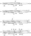
実施形態を説明する前に、基礎となる予備的事項について説明する。図1(a)に示すように、予備的事項の光導波路装置では、配線基板100の上に光導波路300が配置されている。配線基板100では、基板120の上に下側配線層200が形成されている。
Prior to describing the embodiment, preliminary items that serve as a basis will be described. As shown in FIG. 1A, in the preliminary optical waveguide device, an
基板120及び下側配線層200の上には、絶縁樹脂からなる層間絶縁層140が形成されている。層間絶縁層140の上には上側配線層220が形成されている。層間絶縁層140には厚み方向に貫通する第1ビア導体VC1及び第2ビア導体VC2が形成されている。下側配線層200と上側配線層220とが第1、第2ビア導体VC1,VC2を介して相互接続されている。
An
図1(b)は図1(a)を平面視した様子を模式的に描いた平面図である。図1(b)の平面図に示すように、光導波路300は複数の第1光路L1と複数の第2光路L2を備えている。第1光路L1と第2光路L2とは交互に並んで配置されている。
FIG. 1B is a plan view schematically illustrating the state of FIG. As shown in the plan view of FIG. 1B, the
各第1光路L1の所定部に第1光路変換ミラーM1が設けられ、各第2光路用コア層L2の所定部に第2光路変換ミラーM2が設けられている。 A first optical path conversion mirror M1 is provided in a predetermined portion of each first optical path L1, and a second optical path conversion mirror M2 is provided in a predetermined portion of each second optical path core layer L2.
そして、配線基板100の上に、光導波路300の第1光路L1に光結合された第1発光素子400が配置されている。また、配線基板100の上に、第2光路L2に光結合された第2発光素子420が配置されている。
On the
第1発光素子400のバンプ電極400aが光導波路300の開口部を介して配線基板100の上側配線層220に接続されている。第1発光素子400の下側にはアンダーフィル樹脂410が充填されている。
The
また同様に、第2発光素子420のバンプ電極420aが光導波路300の開口部を介して配線基板100の上側配線層220に接続されている。第2発光素子420の下側にはアンダーフィル樹脂430が充填されている。
Similarly, the
第1、第2発光素子400,420は複数の発光部Eをそれぞれ備えている。第1発光素子400の各発光部Eは第1光路L1の第1光路変換ミラーM1に光結合されている。また、第2発光素子420の各発光部Eは第2光路L2の第2光路変換ミラーM2に光結合されている。
The first and second
このように、第1発光素子400の発光部Eと第2発光素子420の発光部Eとが第1、第2光路L1,L2に交互に光結合されている。
As described above, the light emitting part E of the first
ここで、第1発光素子400の発光部Eの配置ピッチは250μm程度である。このため、一つの第1発光素子400を配置する場合は、光導波路300の光路の配置ピッチも250μmとなり、光路の配置ピッチをこれ以上狭くすることは困難である。
Here, the arrangement pitch of the light emitting portions E of the first
そこで、第1光素子400が光結合される複数の第1光路L1の間の領域に第2光路L2を配置し、その第2光路L2に第2発光素子420を光結合させている。
Therefore, the second optical path L2 is disposed in a region between the plurality of first optical paths L1 to which the first
これにより、複数の第1光路L1と複数の第2光路L2とを組み合わせた光路の配置ピッチは、第1発光素子400の発光部Eの半分の配置ピッチ(125μm)になる。これにより、光導波路300の光路の狭ピッチ化を図ることができる。
As a result, the arrangement pitch of the optical paths obtained by combining the plurality of first optical paths L1 and the plurality of second optical paths L2 is half the arrangement pitch (125 μm) of the light emitting portion E of the first
また、配線基板100の上側配線層220に第1ドライバ素子500のバンプ電極500aが接続されている。第1ドライバ素子500の下側にはアンダーフィル樹脂510が充填されている。第1発光素子400は上側配線層220を介して第1ドライバ素子500に電気的に接続されている。
Further, the
また同様に、配線基板100の上側配線層220に第2ドライバ素子520のバンプ電極520aが接続されている。第2ドライバ素子520の下側にはアンダーフィル樹脂530が充填されている。第2発光素子420は、上側配線層220、第1ビア導体VC1、下側配線層200、第2ビア導体VC2、及び上側配線層220を介して第2ドライバ素子520に電気的に接続されている。
Similarly, the
予備的事項の光導波路装置では、第1、第2発光素子400,420と第1、第2ドライバ素子500,520とをそれぞれ電気的に接続するために、第1、第2ビア導体VC1,VC2を備えた多層配線構造の配線基板100を使用している。
In the preliminary optical waveguide device, the first and second via conductors VC1 and VC1 are electrically connected to the first and second light-emitting
このため、高速な電気伝送時に、第1、第2ビア導体VC1,VC2での反射などによって伝送損失が発生し、高速な信号伝送が阻害される。 For this reason, during high-speed electrical transmission, transmission loss occurs due to reflection at the first and second via conductors VC1 and VC2, and high-speed signal transmission is hindered.
また、配線基板100の第1、第2ビア導体VC1,VC2を形成する際には、まず、パターン化された上側配線層220に繋がるように基板にビアホールを形成する。さらに、無電解めっきによってビアホール内にビア導体VCを形成して下側配線層200と上側配線層220とを接続する手法が採用される。
When forming the first and second via conductors VC1 and VC2 of the
このとき、上側配線層220の表面にも無電解めっきが施される。このため、無電解めっきによって上側配線層220の幅や厚みがばらついて寸法精度が低下することからインピーダンスの不整合が生じ、信号伝送特性が劣化する。
At this time, electroless plating is also applied to the surface of the
発光素子とドライバ素子を接続する形態を説明したが、受光素子とアンプ素子を接続する場合も同様な問題が発生する。 Although the embodiment in which the light emitting element and the driver element are connected has been described, the same problem occurs when the light receiving element and the amplifier element are connected.
以下に説明する実施形態では、前述した不具合を解消することができる。 In the embodiment described below, the above-described problems can be solved.
(実施形態)
図2(a)は実施形態の光導波路装置を示す断面図、図2(b)は同じく光導波路装置を示す平面図、図2(c)は図2(a)をA方向からみた側面図である。また、図4〜図6は実施形態の光導波路装置の製造方法を示す断面図である。
(Embodiment)
2A is a sectional view showing the optical waveguide device of the embodiment, FIG. 2B is a plan view showing the optical waveguide device, and FIG. 2C is a side view of FIG. 2A viewed from the A direction. It is. 4 to 6 are cross-sectional views showing a method for manufacturing the optical waveguide device of the embodiment.
図2(a)及び(c)に示すように、実施形態の光導波路装置1では、配線基板20の下に光導波路10が配置されている。光導波路10は、第1クラッド層12と、その上に形成されたコア層14と、それを被覆して第1クラット層12の上に形成された第2クラッド層16とを備え、コア層14が第1、第2クラッド層12,16で囲まれた構造を有する。
As shown in FIGS. 2A and 2C, in the
コア層14の屈折率は、第1クラッド層12及び第2クラッド層16の屈折率よりも高くなるように設定されている。
The refractive index of the
図2(b)は図2(a)を平面視した様子を模式的に描いた平面図である。図2(b)の例では、コア層14は、4本の第1光路用コア層L1と、それらの間の領域にそれぞれ配置された4本の第2光路用コア層L2を備えて配置されている。
FIG. 2B is a plan view schematically illustrating the state of FIG. In the example of FIG. 2B, the
このように、第1光路コア層L1と第2光路用コア層L2とが互い違いになるように水平方向に交互に並んで配置されている。 Thus, the first optical path core layers L1 and the second optical path core layers L2 are alternately arranged in the horizontal direction so as to be alternated.
後述するように、複数の第1光路用コア層L1に第1光素子が光結合され、複数の第2光路用コア層L2に第2光素子が光結合される。 As will be described later, the first optical element is optically coupled to the plurality of first optical path core layers L1, and the second optical element is optically coupled to the plurality of second optical path core layers L2.
図2(a)及び(b)に示すように、第1光路用コア層L1には第1光素子に光結合される第1光路変換ミラーM1がそれぞれ設けられている。また、第2光路用コア層L2には、第2光素子に光結合される第2光路変換ミラーM2がそれぞれ設けられている。 As shown in FIGS. 2A and 2B, the first optical path core layer L1 is provided with a first optical path conversion mirror M1 that is optically coupled to the first optical element. The second optical path core layer L2 is provided with a second optical path conversion mirror M2 that is optically coupled to the second optical element.
光導波路10の上に配置された配線基板20は、基板22と、その下面に形成された下側配線層24と、その上面に形成された上側配線層26とを備えている。また、基板22は、光素子と光導波路10とを光結合させるための光透過用開口部22aを第1、第2光路変換ミラーM1,M2の上に備えている。さらに、基板22は、光素子などを配線基板20の下側配線層24に接続するための接続用開口部22bを下側配線層24の上に備えている。
The
基板22としては、ポリイミドフィルムなどのフレキシブルな薄膜材料を使用することが好ましい。あるいは、ガラスエポキシ樹脂などのリジット基板を使用しても差し支えない。
As the
そして、配線基板20の上側配線層26に第1光素子30のバンプ電極30aが接続されている。第1光素子30と配線基板20との隙間及び光透過用開口部22aに透明なアンダーフィル樹脂31が充填されている。第1光素子30は光透過用開口部22aを介して第1光路用コア層L1に光結合されている。
A
また、第2光素子32のバンプ電極32aが配線基板20の接続用開口部22bを介して、その底に配置された下側配線層24に接続されている。第2光素子32と配線基板20との隙間及び光透過用開口部22aに透明なアンダーフィル樹脂33が充填されている。第2光素子32は光透過用開口部22aを介して第2光路用コア層L2に光結合されている。
Further, the
図2(b)の平面図では、下側配線層24は太破線で描かれており、第1回路素子40の周りで省略されている。また、図2(a)の配線基板20の光透過用開口部22a、接続用開口部22b、及び第1、第2光素子30,32の下側のアンダーフィル樹脂31,33が省略されている。
In the plan view of FIG. 2B, the
第1、第2光素子30,32は、発光素子又は受光素子のいずれかの同一素子である。発光素子としては、面発光レーザ(VCSEL:Vertical Cavity Surface Emitting Laser)が好適に使用される。また、受光素子としては、フォトダイオードが好適に使用される。
The 1st, 2nd
以下では、第1、第2光素子30,32が発光素子からなる形態を例に挙げて説明する。図2(a)及び(b)に示すように、第1、第2光素子30,32が発光素子からなる場合は、第1、第2光素子30,32は下面に複数の発光部Eを備えている。第1光素子30の発光部Eが第1光路用コア層L1に設けられた第1光路変換ミラーM1にそれぞれ光結合される。
Hereinafter, the first and second
このとき、予備的事項でも説明したように、第1光素子30の発光部Eの配置ピッチは250μm程度である。このため、一つの第1光素子30のみを配置する場合は、光導波路10のコア層14の配置ピッチも250μmとなり、それよりも狭ピッチにすることは困難である。
At this time, as described in the preliminary matter, the arrangement pitch of the light emitting portions E of the first
そこで、本実施形態では、第1光路用コア層L1の間の領域に第2光路用コア層L2をそれぞれ配置している。そして、第2光路用コア層L2に設けられた第2光路変換ミラーM2に第2光素子32の発光部Eが光結合するように第2光素子32を配置している。
Therefore, in the present embodiment, the second optical path core layer L2 is disposed in a region between the first optical path core layers L1. And the 2nd
このように、第1光素子30に光結合される第1光路用コア層L1と、第2光素子32に光結合される第2光路用コア層L2とを水平方向に交互に配置している。これにより、得られる光路の配置ピッチを第1光素子30の発光部Eの配置ピッチの半分に狭小化することができ、光導波路装置の高密度化及び小型化を図ることができる。
As described above, the first optical path core layer L1 optically coupled to the first
第1、第2光素子30,32が受光素子の場合も、同様に、第1光素子30の複数の受光部が各第1光路用コア層L1に光結合されるように、第1光素子30が配置される。さらに、第1光路用コア層L1の間の領域に配置された各第2光路用コア層L2に第2光素子32の複数の受光部がそれぞれ光結合するように、第2光素子32が配置される。
Similarly, in the case where the first and second
また、配線基板20の上側配線層26には第1回路素子40のバンプ電極40aが接続されている。第1回路素子40と配線基板20との隙間にアンダーフィル樹脂41が充填されている。このようにして、第1光素子30は配線基板20の上側配線層26を介して第1回路素子40に電気的に接続されている。
A
また、第2回路素子42のバンプ電極42aが配線基板20の接続用開口部22bを介して、その底に配置された下側配線層24に接続されている。第2回路素子42と配線基板20との隙間及び接続用開口部22bにアンダーフィル樹脂43が充填されている。このようにして、第2光素子32は配線基板20の下側配線層24を介して第2回路素子42に電気的に接続されている。
Further, the
図2(a)の平面図では、第1、第2回路素子40,42の下側のアンダーフィル樹脂41,43、及び基板22の接続用開口部22bが省略されている。
In the plan view of FIG. 2A, the underfill resins 41 and 43 below the first and
第1、第2光素子30,32が発光素子の場合は、第1、第2回路素子40、42としてドライバ素子が使用される。あるいは、第1、第2光素子30,32が受光素子の場合は、第1、第2回路素子40,42としてアンプ素子(TIA : Transimpedance Amplifierなど)が使用される。
When the first and second
このように、本実施形態の光導波路装置1では、配線基板20はビア導体を備えておらず、第2光素子32と第2回路素子42とは、配線基板20の接続用開口部22bを介して下側配線層24に直接接続されている。
As described above, in the
このため、高速電気伝送時にビア導体での反射などによる伝送損失の発生が抑制され、高速で高品質な信号伝送を実現することができる。 For this reason, the occurrence of transmission loss due to reflection on via conductors during high-speed electrical transmission is suppressed, and high-speed and high-quality signal transmission can be realized.
また、配線基板20の下側、上側配線層24,26は、めっき法を使用することなく、基板22の両面に形成された厚み精度の高い銅箔などをフォトリソグラフィでパターニングすることにより得られる。このため、下側、上側配線層24,26の幅や厚みのばらつきが抑えられて寸法精度を向上させることができるので、伝送経路でのインピーダンス整合を得ることができる。
Further, the lower and upper wiring layers 24 and 26 of the
また、第1、第2光素子30,32は、第1光路用コア層L1及び第2光路用コア層L2にそれぞれ交互に光結合するように横方向に並んで配置されている。このため、第1、第2光素子30,32の発光部Eの配置ピッチの半分のピッチの光路を配置することができるため、高密度な光導波路を実現することができる。
The first and second
図3(a)には、配線基板20の上側配線層26のレイアウトの一例が平面図で示されている。図3(a)に示すように、上側配線層26は、白パターンで描かれた信号用配線層26aと斜線ハッチングされて描かれたグランド用配線層26bとを備えている。
FIG. 3A is a plan view showing an example of the layout of the
図2(a)を加えて参照すると、信号用配線層26a及びグランド用配線層26bの第1接続パッドP1の群に第1光素子30のバンプ電極30aが接続される。また、信号用配線層24a及びグランド用配線層24bの第2接続パッドP2及び第3接続パッドP3の群に第1回路素子40のバンプ電極40aが接続される。
2A, the
このようにして、第1光素子30が上側配線層26を介して第1回路素子40に電気的に接続される。
In this way, the first
また、図3(b)には、配線基板20の下側配線層24のレイアウトの一例が平面図で示されている。図3(b)に示すように、下側配線層24は、白パターンで描かれた信号用配線層24aと斜線ハッチングされて描かれたグランド用配線層24bとを備えている。
FIG. 3B is a plan view showing an example of the layout of the
図2(a)を加えて参照すると、信号用配線層24a及びグランド用配線層24bの第1接続パッドPの群に第2光素子32のバンプ電極32aが接続される。また、信号用配線層24a及びグランド用配線層24bの第2接続パッドP2及び第3接続パッドP3の群に第2回路素子42のバンプ電極42aが接続される。
2A, the
このようにして、第2光素子32が下側側配線層24を介して第2回路素子42に電気的に接続される。
In this way, the second
次に、本実施形態の光導波路装置1の光伝搬について図2(a)を参照しながら説明する。第1、第2光素子30,32が発光素子の場合は、第1、第2回路素子40,42がドライバ素子として配置される。そして、第1、第2回路素子40,42から出力される電気信号が第1、第2光素子30,32にそれぞれ供給され、それらの発光部Eから下側に光が同時に出射される。
Next, the light propagation of the
第1、第2光素子30,32からそれぞれ出射される光は、アンダーフィル樹脂31,33、第2クラッド層16及びコア層14を透過して第1、第2光路変換ミラーM1,M2にそれぞれ到達する。さらに、第1、第2光路変換ミラーM1,M2で光が反射され、光路が90°変換されてコア層14に入射する。
The light emitted from the first and second
次いで、コア層14に入射した光は、コア層14内で全反射を繰り返して伝播し、別の光路変換ミラーによって他端側の受光素子に入力される。あるいは、コネクタ部が接続される場合は、コア層14を伝搬する光がコネクタ部に連結される外部の光ファイバなどに入射される。
Next, the light incident on the
第1、第2光素子30,32が受光素子の場合は、第1、第2回路素子40,42がアンプ素子として配置される。この場合は、上記した光経路と逆方向に光伝搬され、受光素子の受光部に光が入射される。さらに、受光素子は光信号を電気信号に変換し、アンプ素子に電気信号が供給される。
When the first and second
次に、実施形態の光導波路装置の製造方法について説明する。図4(a)に示すように、まず、基板22の両面に銅箔21が貼付された積層体5を用意する。基板22はポリイミドフィルムなどのフレキシブル材から形成され、その厚みは好適には10〜30μmであり、例えば20μm程度である。また、銅箔21の厚みは好適には5μm〜20μmであり、例えば9μm程度である。
Next, a method for manufacturing the optical waveguide device of the embodiment will be described. As shown in FIG. 4A, first, a
銅箔21は、その厚みの面内のばらつきが±10%以下に抑えられており、めっき法で形成される銅層よりも厚みの寸法精度が高い。
The in-plane variation of the thickness of the
なお、金属層として銅箔21を例示するが、配線層として機能する金属層が両面に均一に形成された基板を用意すればよい。
In addition, although the
次いで、図4(b)に示すように、積層体5の両面側に、下側、上側配線層24,26を得るためのレジストパターン23をフォトリソグラフィに基づいてそれぞれ形成する。
Next, as shown in FIG. 4B, resist
さらに、図4(c)に示すように、積層体5の両面側において、レジストパターン23をマスクにして銅箔21をウェットエッチングする。銅箔21のエッチャントとしては、塩化第二銅水溶液、又は塩化第二鉄水溶液などがある。その後に、レジストパターン23が除去される。
Further, as shown in FIG. 4C, the
これにより、基板22の下面に下側配線層24が形成され、上面に上側配線層26が形成される。
As a result, the
続いて、基板22をレーザなどで貫通加工することにより、基板22に第1、第2光素子30,32を光導波路10に光結合させるための光透過用開口部22aを形成する。また同時に、基板22に第2光素子32及び第2回路素子42を接続するための接続用開口部22bを形成する。これにより、配線基板20が得られる。
Subsequently, by penetrating the
次いで、図5(a)に示すように、図4(d)の配線基板20を上下反転させる。さらに、図5(b)に示すように、配線基板20の上に第2クラッド層16を得るための感光性樹脂層(不図示)を形成し、フォトリソグラフィに基づいて露光/現像を行う。その後に、感光性樹脂層を100℃〜140℃程度の加熱処理によって硬化させる。
Next, as shown in FIG. 5A, the
これより、配線基板20の下側配線層24側(図5(a)では上側)に第2クラッド層16が形成される。第2クラッド層16の厚みは、例えば10μm〜30μm程度である。
Thus, the
感光性樹脂層としては、UV硬化型エポキシ樹脂などが好適に使用される。感光性樹脂層の形成方法としては、半硬化状態(B−ステージ)の感光性樹脂シートを貼付してもよいし、あるいは、液状の感光性樹脂を塗布してもよい。 As the photosensitive resin layer, a UV curable epoxy resin or the like is preferably used. As a method for forming the photosensitive resin layer, a semi-cured (B-stage) photosensitive resin sheet may be applied, or a liquid photosensitive resin may be applied.
後述するコア層14及び第1クラッド層12を形成する工程においても同様な樹脂が好適に使用される。
Similar resin is also preferably used in the step of forming the
続いて、図5(c)に示すように、第2クラッド層16の上にコア層を得るための感光性樹脂層(不図示)を形成する。さらに、フォトリソグラフィに基づいて露光/現像を行った後に、感光性樹脂層を100℃〜140℃程度の加熱処理によって硬化させる。
Subsequently, as shown in FIG. 5C, a photosensitive resin layer (not shown) for obtaining a core layer is formed on the
これにより、第1クラッド層12の上にコア層14が複数の帯状パターンとして並んで形成される。前述したように、コア層14は、第1光路用コア層L1と、それらの間の領域にそれぞれ配置された第2光路用コア層L2とを備えて形成される。
As a result, the
次いで、図5(d)に示すように、コア層14をレーザで局所的に加工することにより、コア層14の第1光路用コア層L1(図2(b))にV字状の第1溝部14aを形成する。第1溝部14aは光路変換するための第1傾斜面IS1を備えて形成される。
Next, as shown in FIG. 5D, the
また同時に、コア層14の第2光路用コア層L2(図2(b))にV字状の第2溝部14bが形成される。第2溝部14bは光路変換するための第2傾斜面IS2を備えて形成される。第1、第2傾斜面IS1,IS2は、配線基板20の表面に対して好適には45°で傾斜して形成される。
At the same time, the V-shaped
次いで、図6(a)に示すように、マスク蒸着などにより、コア層14の第1、第2傾斜面IS1,IS2(図5(d))に光反射性の金属層を部分的に形成して第1、第2光路変換ミラーM1,M2を得る。光反射性の金属として、金又はアルミニウムなどがある。
Next, as shown in FIG. 6A, a light-reflective metal layer is partially formed on the first and second inclined surfaces IS1 and IS2 (FIG. 5D) of the
第1、第2光路変換ミラーM1,M2の別の形成方法としては、傾斜面に光反射性の金属層が形成された透明な三角柱状の光学部品を未硬化状態のコア層に埋め込んだ後に、コア層を硬化させてもよい。これにより、光学部品の傾斜面の金属層が光路変換ミラーとして機能する。 Another method for forming the first and second optical path conversion mirrors M1 and M2 is after embedding a transparent triangular prism-shaped optical component having a light-reflective metal layer formed on an inclined surface in an uncured core layer. The core layer may be cured. Thereby, the metal layer on the inclined surface of the optical component functions as an optical path conversion mirror.
続いて、図6(b)に示すように、第2クラッド層16及びコア層14の上に第1クラッド層12を得るための感光性樹脂層(不図示)を形成し、フォトリソグラフィに基づいて露光/現像を行う。その後に、感光性樹脂層を100℃〜140℃程度の加熱処理によって硬化させる。
Subsequently, as shown in FIG. 6B, a photosensitive resin layer (not shown) for obtaining the
これより、コア層14を被覆する第1クラッド層12が第2クラッド層16の上に形成される。第1クラッド層12はコア層14に形成された第1、第2光路変換ミラーM1,M2の段差を埋め込み、その上面が平坦になって形成される。第1クラッド層12の厚みは、コア層14上で例えば10μm〜30μm程度になるように設定される。
Thus, the
その後に、図6(c)に示すように、図6(b)の構造体を上下反転させる。そして、第1光素子30のバンプ電極30aを配線基板20の上側配線層26にはんだなどで接続する。また、第2光素子32のバンプ電極32aを配線基板20の接続用開口部22bを介して下側配線層24にはんだなどで接続する。
Thereafter, as shown in FIG. 6C, the structure of FIG. 6B is turned upside down. Then, the
さらに、第1回路素子40のバンプ電極40aを配線基板20の上側配線層26にはんだなどで接続する。また、第2回路素子42のバンプ電極42aを配線基板20の接続用開口部22bを介して下側配線層24にはんだなどで接続する。
Further, the
このようにして、第1光素子30と第1回路素子40とが上側配線層26を介して電気的に接続された構造を得る。また、第2光素子32が接続用開口部22bを介して下側配線層24に接続され、第2光素子32と第2回路素子42とが下側配線層24を介して電気的に接続される構造を得る。
In this manner, a structure in which the first
第1、第2光素子30,32、及び第1、第2回路素子40,42の下側に充填されるアンダーフィル樹脂31,33,41,43(図2(a))は、各素子を実装するごとに形成してもよいし、一括して形成してもよい。
The underfill resins 31, 33, 41, and 43 (FIG. 2A) filled below the first and second
以上により、図2(a)及び(b)の本実施形態の光導波路装置1を製造することができる。
As described above, the
なお、前述した製造方法の他に、仮基板上で光導波路を作成した後に、光導波路を仮基板から剥離し、図5(a)の配線基板20の上に接着層で光導波路10を接着してもよい。つまり、配線基板20の上に光導波路10を作り込んで形成してもよいし、配線基板20の上に光導波路10の部品を接着して形成してもよい。
In addition to the manufacturing method described above, after creating the optical waveguide on the temporary substrate, the optical waveguide is peeled off from the temporary substrate, and the
本実施形態の光導波路装置の製造方法では、配線基板20の下側、上側配線層24,26は、厚み精度の高い銅箔21がフォトリソグラフィ及びウェットエッチングによってパターニングされて形成される。
In the manufacturing method of the optical waveguide device of the present embodiment, the lower and upper wiring layers 24 and 26 of the
従って、下側、上側配線層24,26をめっき法に基づいて形成する場合よりも幅や厚みのばらつきを抑えることができるため、伝送経路でのインピーダンス整合を得やすくすることができる。その結果、信号の伝送損失が抑制され、良好な信号伝送特性を得ることができる。 Therefore, since variations in width and thickness can be suppressed as compared with the case where the lower and upper wiring layers 24 and 26 are formed based on the plating method, impedance matching in the transmission path can be easily obtained. As a result, signal transmission loss is suppressed, and good signal transmission characteristics can be obtained.
次に、図7を参照しながら、本実施形態の光導波路装置1をマザーボードなどの電子基板に接続する例について説明する。図7に示すように、両側に壁部Wを備えて、一端側及び上側が開口されたキャビティCを備えたガラスなどからなる透明ケース60を用意する。そして、透明ケース60のキャビティCに図2(a)の光導波路装置1が配置されている。
Next, an example in which the
さらに、透明ケース60の他端側に光接続用のコネクタ部50が設けられている。コネクタ部50に、外部の光ファイバなどが光導波路10に位置合わせされて接続され、光導波路10に光結合するようになっている。
Furthermore, a
光導波路装置1の配線基板20は透明ケース60の先端から外部に延びた延在部20aを備えている。配線基板20の延在部20aがフレキシブルコネクタ70に接続されている。フレキシブルコネクタ70は、支持部70aと、可動する蓋部70bとを有する。フレキシブルコネクタ70の支持部70aの上に配線基板20の延在部20aを配置し、蓋部70bを支持部70aに固定することで配線基板20とフレキシブルコネクタ70とが接続される。
The
配線基板20の延在部20aの上側配線層26及び下側配線層24にフレキシブルコネクタ70の第1配線層72及び第2配線層74が接続されている。
The
さらに、フレキシブルコネクタ70の第1配線層72及び第2配線層74が電子基板80の配線層82に接続されている。
Further, the
このように、本実施形態の光導波路装置1は、透明ケース60に収容された状態で、配線基板20がフレキシブルコネクタ70を介してマザーボードなどの電子基板80に電気的に接続される。
As described above, in the
ここで、比較例として、前述した図1(a)で説明した予備的事項の光導波路装置をマザーボードなどの電子基板に接続する場合に言及する。図1(a)の光導波路装置では、図示されていないが、基板120にも下側配線層200に接続されるビア導体が接続され、基板120の下面に外部端子としてはんだボールが搭載される。
Here, as a comparative example, reference is made to the case where the optical waveguide device of the preliminary matter described in FIG. 1A is connected to an electronic substrate such as a mother board. In the optical waveguide device of FIG. 1A, although not shown, via conductors connected to the
そして、図1(a)の光導波路装置のはんだボールが電子基板に電気的に接続される。この比較例では、伝送経路にはんだボールが存在するため、インピーダンス整合をとりづらい構造となり、効率よく信号を伝送することが困難になる。 Then, the solder balls of the optical waveguide device of FIG. 1A are electrically connected to the electronic substrate. In this comparative example, since there is a solder ball in the transmission path, it is difficult to achieve impedance matching, and it is difficult to efficiently transmit a signal.
しかしながら、本実施形態の図7の形態の例では、はんだボールを使用することなく銅などからなる配線層同士を接続するため、伝送経路でのインピーダンス整合をとりやすい構造となり、効率よく信号を伝送することができる。 However, in the example of the embodiment of FIG. 7 of the present embodiment, since the wiring layers made of copper or the like are connected without using a solder ball, a structure that facilitates impedance matching in the transmission path is achieved, and signals are transmitted efficiently. can do.
次に、図8を参照しながら、本実施形態の光導波路装置1をマザーボードなどの電子基板に接続する別の例について説明する。
Next, another example of connecting the
図8において図7と異なる点は、図7で光導波路装置1内に配置された第1回路素子40及び第2回路素子42が外部の電子基板80に配置されている。図8においてその他の要素は図7と同一であるので、同一符号を付してその詳しい説明を省略する。
8 differs from FIG. 7 in that the
第1光素子30は、配線基板20の上側配線層26、フレキシブルコネクタ70の第1配線層72、及び電子基板80の配線層82を介して第1回路素子40のバンプ電極40aに電気的に接続されている。
The first
また、第2光素子32は、配線基板20の下側配線層24、フレキシブルコネクタ70の第2配線層74、及び電子基板80の配線層82を介して第2回路素子42のバンプ電極40bに電気的に接続される。
Further, the second
このように、第1回路素子40及び第2回路素子42がマザーボードなどの外部の電子基板80に配置された形態としてもよい。そして、電子基板80上に配置された第1回路素子40が上側配線層26などを介して配線基板20上の第1光素子30に電気的に接続される。また、電子基板80上に配置された第2回路素子42が下側配線層24などを介して配線基板20上の第2光素子32に電気的に接続される。
As described above, the
この形態では、光導波路装置は、第1回路素子40及び第2回路素子42が配置された電子基板80及びフレキシブルコネクタ70を備えて構築される。
In this embodiment, the optical waveguide device is constructed by including the
図8の形態の例においても、はんだボールを使用しないため、伝送経路でのインピーダンス整合をとりやすい構造となり、効率よく信号を伝送することができる。 Also in the example of the form of FIG. 8, since solder balls are not used, it is easy to achieve impedance matching in the transmission path, and signals can be transmitted efficiently.
1…光導波路装置、10…光導波路、12…第1クラッド層、14…コア層、14a,14b…溝部、16…第2クラッド層、20…配線基板、20a…延在部、22…基板、22a…光透過用開口部、22b…接続用開口部、23…レジストパターン、24…下側配線層、24a,26a…信号用配線層、24b,26b…グランド用配線層、26…上側配線層、30…第1光素子、30a,32a,40a,42a…バンプ電極、31,33,41,43…アンダーフィル樹脂、32…第2光素子、40…第1回路素子、42…第2回路素子、50…コネクタ部、60…透明ケース、70…フレキシブルコネクタ、70a…支持部、70b…蓋部、72…第1配線層、74…第2配線層、80…電子基板、82…配線層、C…キャビティ、E…発光部、L1…第1光路用コア層、L2…第2光路用コア層、M1…第1光路変換ミラー、M2…第2光路変換ミラー、P1,P2、P3…接続パッド、IS1,IS2…傾斜面、W…壁部。
DESCRIPTION OF
Claims (7)
前記基板の上面に形成された上側配線層と、
前記基板の下面に形成された下側配線層と、
前記基板に形成された開口部と
を備えた配線基板と、
前記配線基板の下側配線層側に形成された光導波路と、
前記配線基板の上側配線層に接続された第1光素子と、
前記上側配線層を介して前記第1光素子に電気的に接続された第1回路素子と、
第2光素子のバンプ電極が前記配線基板の開口部に挿通されて前記下側配線層に電気的に接続された前記第2光素子と、
第2回路素子のバンプ電極が前記配線基板の開口部に挿通されて前記下側配線層に接続され、前記下側配線層を介して前記第2光素子に電気的に接続された前記第2回路素子とを有することを特徴とする光導波路装置。 A substrate,
An upper wiring layer formed on the upper surface of the substrate;
A lower wiring layer formed on the lower surface of the substrate;
A wiring board having an opening formed in the board;
An optical waveguide formed on the lower wiring layer side of the wiring board;
A first optical element connected to the upper wiring layer of the wiring board;
A first circuit element electrically connected to the first optical element through the upper wiring layer;
The second optical element in which the bump electrode of the second optical element is inserted into the opening of the wiring board and electrically connected to the lower wiring layer ;
Bump electrodes of the second circuit element are inserted into the openings of the wiring board and connected to the lower wiring layer, and are electrically connected to the second optical element through the lower wiring layer. An optical waveguide device comprising a circuit element .
前記両面の各金属層をパターニングすることにより、上側配線層と下側配線層とを形成する工程と、
前記基板に開口部を形成する工程と、
前記基板の前記下側配線層側に光導波路を形成する工程と、
第1光素子と第1回路素子とが前記上側配線層を介して電気的に接続され、かつ、第2光素子が前記基板の開口部を介して前記下側配線層に接続され、前記第2光素子と第2回路素子とが前記下側配線層を介して電気的に接続される構造を得る工程とを有し、
前記第2光素子のバンプ電極を前記配線基板の開口部に挿通させて前記下側配線層に電気的に接続すると共に、
前記第2回路素子のバンプ電極を前記配線基板の開口部に挿通させて前記下側配線層に接続することを特徴とする光導波路装置の製造方法。 Preparing a substrate having a metal layer formed on both sides;
Forming an upper wiring layer and a lower wiring layer by patterning each of the metal layers on both sides;
Forming an opening in the substrate;
Forming an optical waveguide on the lower wiring layer side of the substrate;
The first optical element and the first circuit element are electrically connected via the upper wiring layer, and the second optical element is connected to the lower wiring layer via the opening of the substrate, A step of obtaining a structure in which the two optical elements and the second circuit element are electrically connected via the lower wiring layer,
The bump electrode of the second optical element is inserted through the opening of the wiring board and electrically connected to the lower wiring layer,
A method of manufacturing an optical waveguide device, wherein the bump electrode of the second circuit element is inserted into an opening of the wiring board and connected to the lower wiring layer .
前記光導波路は、第1光路用コア層と第2光路用コア層とが水平方向に交互に並んで配置され、
前記構造を得る工程において、
前記第1光素子が前記第1光路用コア層に光結合され、前記第2光素子が前記第2光路用コア層に光結合されることを特徴とする請求項6に記載の光導波路装置の製造方法。 In the step of forming the optical waveguide,
In the optical waveguide, the first optical path core layer and the second optical path core layer are alternately arranged in the horizontal direction,
In the step of obtaining the structure,
7. The optical waveguide device according to claim 6 , wherein the first optical element is optically coupled to the first optical path core layer, and the second optical element is optically coupled to the second optical path core layer. Manufacturing method.
Priority Applications (2)
| Application Number | Priority Date | Filing Date | Title |
|---|---|---|---|
| JP2012277550A JP6084027B2 (en) | 2012-12-20 | 2012-12-20 | Optical waveguide device and manufacturing method thereof |
| US14/105,598 US9075206B2 (en) | 2012-12-20 | 2013-12-13 | Optical waveguide device |
Applications Claiming Priority (1)
| Application Number | Priority Date | Filing Date | Title |
|---|---|---|---|
| JP2012277550A JP6084027B2 (en) | 2012-12-20 | 2012-12-20 | Optical waveguide device and manufacturing method thereof |
Publications (3)
| Publication Number | Publication Date |
|---|---|
| JP2014122929A JP2014122929A (en) | 2014-07-03 |
| JP2014122929A5 JP2014122929A5 (en) | 2015-12-24 |
| JP6084027B2 true JP6084027B2 (en) | 2017-02-22 |
Family
ID=50974763
Family Applications (1)
| Application Number | Title | Priority Date | Filing Date |
|---|---|---|---|
| JP2012277550A Active JP6084027B2 (en) | 2012-12-20 | 2012-12-20 | Optical waveguide device and manufacturing method thereof |
Country Status (2)
| Country | Link |
|---|---|
| US (1) | US9075206B2 (en) |
| JP (1) | JP6084027B2 (en) |
Families Citing this family (6)
| Publication number | Priority date | Publication date | Assignee | Title |
|---|---|---|---|---|
| US10209464B2 (en) * | 2014-10-17 | 2019-02-19 | Cisco Technology, Inc. | Direct printed circuit routing to stacked opto-electrical IC packages |
| US9786641B2 (en) | 2015-08-13 | 2017-10-10 | International Business Machines Corporation | Packaging optoelectronic components and CMOS circuitry using silicon-on-insulator substrates for photonics applications |
| US9721812B2 (en) * | 2015-11-20 | 2017-08-01 | International Business Machines Corporation | Optical device with precoated underfill |
| WO2021100978A1 (en) * | 2019-11-20 | 2021-05-27 | 엘지디스플레이 주식회사 | Side wiring manufacturing apparatus, side wiring manufacturing method, and display apparatus manufacturing method |
| US11664355B2 (en) | 2019-12-02 | 2023-05-30 | Seoul Semiconductor Co., Ltd. | Display apparatus |
| JP7477306B2 (en) * | 2020-01-17 | 2024-05-01 | 日東電工株式会社 | Optical-electrical transmission composite module and optical-electrical hybrid board |
Family Cites Families (19)
| Publication number | Priority date | Publication date | Assignee | Title |
|---|---|---|---|---|
| JPH11135891A (en) * | 1997-10-31 | 1999-05-21 | Matsushita Electric Ind Co Ltd | Semiconductor light emitting device and manufacturing method thereof, optical fiber with light emitting device, optical communication module, and optical communication system |
| US6343171B1 (en) * | 1998-10-09 | 2002-01-29 | Fujitsu Limited | Systems based on opto-electronic substrates with electrical and optical interconnections and methods for making |
| JP2004069798A (en) * | 2002-08-02 | 2004-03-04 | Canon Inc | Photoelectric confluent wiring board having photoelectric confluent viahole |
| JP2004235418A (en) * | 2003-01-30 | 2004-08-19 | Seiko Epson Corp | Optical module, optical communication device, opto-electric hybrid integrated circuit, circuit board, electronic equipment |
| US7070207B2 (en) * | 2003-04-22 | 2006-07-04 | Ibiden Co., Ltd. | Substrate for mounting IC chip, multilayerd printed circuit board, and device for optical communication |
| US7112885B2 (en) * | 2003-07-07 | 2006-09-26 | Board Of Regents, The University Of Texas System | System, method and apparatus for improved electrical-to-optical transmitters disposed within printed circuit boards |
| US7248757B2 (en) * | 2003-12-15 | 2007-07-24 | Canon Kabushiki Kaisha | Method, device and computer program for designing a circuit having electric wires and optical connections |
| US7366368B2 (en) * | 2004-06-15 | 2008-04-29 | Intel Corporation | Optical add/drop interconnect bus for multiprocessor architecture |
| TWI246612B (en) * | 2004-10-12 | 2006-01-01 | Phoenix Prec Technology Corp | Structure having embedded optical electronic components |
| US7492982B2 (en) * | 2006-02-06 | 2009-02-17 | Samsung Electronics Co., Ltd. | Optical module |
| US7373033B2 (en) * | 2006-06-13 | 2008-05-13 | Intel Corporation | Chip-to-chip optical interconnect |
| JP5137393B2 (en) | 2006-12-19 | 2013-02-06 | 古河電気工業株式会社 | Optical coupler |
| US7783141B2 (en) * | 2007-04-04 | 2010-08-24 | Ibiden Co., Ltd. | Substrate for mounting IC chip and device for optical communication |
| US7729570B2 (en) * | 2007-05-18 | 2010-06-01 | Ibiden Co., Ltd. | Photoelectric circuit board and device for optical communication |
| JP2009175418A (en) * | 2008-01-24 | 2009-08-06 | Shinko Electric Ind Co Ltd | Opto-electronic printed wiring board and manufacturing method of same |
| JP5106348B2 (en) * | 2008-10-28 | 2012-12-26 | 日東電工株式会社 | Manufacturing method of opto-electric hybrid module and opto-electric hybrid module obtained thereby |
| US8588558B2 (en) * | 2008-12-05 | 2013-11-19 | General Electric Company | Optical link circuit and method of making same |
| JP5267426B2 (en) * | 2009-11-04 | 2013-08-21 | 住友ベークライト株式会社 | Optical device mounting substrate, opto-electric hybrid substrate, and electronic equipment |
| JP5670169B2 (en) * | 2010-12-15 | 2015-02-18 | 新光電気工業株式会社 | Manufacturing method of optical waveguide |
-
2012
- 2012-12-20 JP JP2012277550A patent/JP6084027B2/en active Active
-
2013
- 2013-12-13 US US14/105,598 patent/US9075206B2/en active Active
Also Published As
| Publication number | Publication date |
|---|---|
| JP2014122929A (en) | 2014-07-03 |
| US9075206B2 (en) | 2015-07-07 |
| US20140177999A1 (en) | 2014-06-26 |
Similar Documents
| Publication | Publication Date | Title |
|---|---|---|
| JP4260650B2 (en) | Photoelectric composite substrate and manufacturing method thereof | |
| KR100720854B1 (en) | Manufacturing method of optoelectronic wiring board, mounting board and optoelectronic wiring board | |
| JP5247880B2 (en) | Photoelectric wiring board and optical module | |
| JP5139375B2 (en) | Optical interface module manufacturing method and optical interface module | |
| JP6084027B2 (en) | Optical waveguide device and manufacturing method thereof | |
| US9081159B2 (en) | Optical waveguide and method of manufacturing the same, and optical waveguide device | |
| JP5395734B2 (en) | Method for manufacturing photoelectric composite substrate | |
| US9201203B2 (en) | Photoelectric composite substrate and method of manufacturing the same | |
| JP5313849B2 (en) | Optical waveguide device and manufacturing method thereof | |
| JP2013205767A (en) | Photo-electric hybrid substrate | |
| JP2011028111A (en) | Optical i/o array module and method of manufacturing the same | |
| JP2016206377A (en) | Optical waveguide device and method of manufacturing the same | |
| US7801399B2 (en) | Method of forming optical waveguide | |
| JP2014203945A (en) | Electronic device, manufacturing method thereof, and electronic apparatus | |
| JP4690870B2 (en) | Opto-electric integrated wiring board and opto-electric integrated wiring system | |
| JP5409441B2 (en) | Optical transmission board and optical module | |
| JP5302177B2 (en) | Optical waveguide substrate and opto-electric hybrid device | |
| JP5976769B2 (en) | Optical waveguide and optical waveguide device | |
| JP2023008206A (en) | wiring board | |
| JP4698728B2 (en) | Opto-electric integrated wiring board and opto-electric integrated wiring system | |
| JP6084024B2 (en) | Optical waveguide device and manufacturing method thereof | |
| JP4691196B2 (en) | Opto-electric integrated wiring board and opto-electric integrated wiring system | |
| TW202515259A (en) | Flexible printed circuit board with embedded optical waveguide structure |
Legal Events
| Date | Code | Title | Description |
|---|---|---|---|
| A521 | Request for written amendment filed |
Free format text: JAPANESE INTERMEDIATE CODE: A523 Effective date: 20151106 |
|
| A621 | Written request for application examination |
Free format text: JAPANESE INTERMEDIATE CODE: A621 Effective date: 20151106 |
|
| A977 | Report on retrieval |
Free format text: JAPANESE INTERMEDIATE CODE: A971007 Effective date: 20160627 |
|
| A131 | Notification of reasons for refusal |
Free format text: JAPANESE INTERMEDIATE CODE: A131 Effective date: 20160719 |
|
| A521 | Request for written amendment filed |
Free format text: JAPANESE INTERMEDIATE CODE: A523 Effective date: 20160909 |
|
| TRDD | Decision of grant or rejection written | ||
| A01 | Written decision to grant a patent or to grant a registration (utility model) |
Free format text: JAPANESE INTERMEDIATE CODE: A01 Effective date: 20170110 |
|
| A61 | First payment of annual fees (during grant procedure) |
Free format text: JAPANESE INTERMEDIATE CODE: A61 Effective date: 20170124 |
|
| R150 | Certificate of patent or registration of utility model |
Ref document number: 6084027 Country of ref document: JP Free format text: JAPANESE INTERMEDIATE CODE: R150 |