JP6388552B2 - 基板処理装置及び基板処理方法 - Google Patents
基板処理装置及び基板処理方法 Download PDFInfo
- Publication number
- JP6388552B2 JP6388552B2 JP2015041499A JP2015041499A JP6388552B2 JP 6388552 B2 JP6388552 B2 JP 6388552B2 JP 2015041499 A JP2015041499 A JP 2015041499A JP 2015041499 A JP2015041499 A JP 2015041499A JP 6388552 B2 JP6388552 B2 JP 6388552B2
- Authority
- JP
- Japan
- Prior art keywords
- gas
- containing gas
- supply unit
- gas supply
- turntable
- Prior art date
- Legal status (The legal status is an assumption and is not a legal conclusion. Google has not performed a legal analysis and makes no representation as to the accuracy of the status listed.)
- Active
Links
Images


Classifications
-
- C—CHEMISTRY; METALLURGY
- C23—COATING METALLIC MATERIAL; COATING MATERIAL WITH METALLIC MATERIAL; CHEMICAL SURFACE TREATMENT; DIFFUSION TREATMENT OF METALLIC MATERIAL; COATING BY VACUUM EVAPORATION, BY SPUTTERING, BY ION IMPLANTATION OR BY CHEMICAL VAPOUR DEPOSITION, IN GENERAL; INHIBITING CORROSION OF METALLIC MATERIAL OR INCRUSTATION IN GENERAL
- C23C—COATING METALLIC MATERIAL; COATING MATERIAL WITH METALLIC MATERIAL; SURFACE TREATMENT OF METALLIC MATERIAL BY DIFFUSION INTO THE SURFACE, BY CHEMICAL CONVERSION OR SUBSTITUTION; COATING BY VACUUM EVAPORATION, BY SPUTTERING, BY ION IMPLANTATION OR BY CHEMICAL VAPOUR DEPOSITION, IN GENERAL
- C23C16/00—Chemical coating by decomposition of gaseous compounds, without leaving reaction products of surface material in the coating, i.e. chemical vapour deposition [CVD] processes
- C23C16/44—Chemical coating by decomposition of gaseous compounds, without leaving reaction products of surface material in the coating, i.e. chemical vapour deposition [CVD] processes characterised by the method of coating
- C23C16/52—Controlling or regulating the coating process
-
- C—CHEMISTRY; METALLURGY
- C23—COATING METALLIC MATERIAL; COATING MATERIAL WITH METALLIC MATERIAL; CHEMICAL SURFACE TREATMENT; DIFFUSION TREATMENT OF METALLIC MATERIAL; COATING BY VACUUM EVAPORATION, BY SPUTTERING, BY ION IMPLANTATION OR BY CHEMICAL VAPOUR DEPOSITION, IN GENERAL; INHIBITING CORROSION OF METALLIC MATERIAL OR INCRUSTATION IN GENERAL
- C23C—COATING METALLIC MATERIAL; COATING MATERIAL WITH METALLIC MATERIAL; SURFACE TREATMENT OF METALLIC MATERIAL BY DIFFUSION INTO THE SURFACE, BY CHEMICAL CONVERSION OR SUBSTITUTION; COATING BY VACUUM EVAPORATION, BY SPUTTERING, BY ION IMPLANTATION OR BY CHEMICAL VAPOUR DEPOSITION, IN GENERAL
- C23C16/00—Chemical coating by decomposition of gaseous compounds, without leaving reaction products of surface material in the coating, i.e. chemical vapour deposition [CVD] processes
- C23C16/44—Chemical coating by decomposition of gaseous compounds, without leaving reaction products of surface material in the coating, i.e. chemical vapour deposition [CVD] processes characterised by the method of coating
- C23C16/455—Chemical coating by decomposition of gaseous compounds, without leaving reaction products of surface material in the coating, i.e. chemical vapour deposition [CVD] processes characterised by the method of coating characterised by the method used for introducing gases into reaction chamber or for modifying gas flows in reaction chamber
-
- C—CHEMISTRY; METALLURGY
- C23—COATING METALLIC MATERIAL; COATING MATERIAL WITH METALLIC MATERIAL; CHEMICAL SURFACE TREATMENT; DIFFUSION TREATMENT OF METALLIC MATERIAL; COATING BY VACUUM EVAPORATION, BY SPUTTERING, BY ION IMPLANTATION OR BY CHEMICAL VAPOUR DEPOSITION, IN GENERAL; INHIBITING CORROSION OF METALLIC MATERIAL OR INCRUSTATION IN GENERAL
- C23C—COATING METALLIC MATERIAL; COATING MATERIAL WITH METALLIC MATERIAL; SURFACE TREATMENT OF METALLIC MATERIAL BY DIFFUSION INTO THE SURFACE, BY CHEMICAL CONVERSION OR SUBSTITUTION; COATING BY VACUUM EVAPORATION, BY SPUTTERING, BY ION IMPLANTATION OR BY CHEMICAL VAPOUR DEPOSITION, IN GENERAL
- C23C16/00—Chemical coating by decomposition of gaseous compounds, without leaving reaction products of surface material in the coating, i.e. chemical vapour deposition [CVD] processes
- C23C16/04—Coating on selected surface areas, e.g. using masks
- C23C16/045—Coating cavities or hollow spaces, e.g. interior of tubes; Infiltration of porous substrates
-
- C—CHEMISTRY; METALLURGY
- C23—COATING METALLIC MATERIAL; COATING MATERIAL WITH METALLIC MATERIAL; CHEMICAL SURFACE TREATMENT; DIFFUSION TREATMENT OF METALLIC MATERIAL; COATING BY VACUUM EVAPORATION, BY SPUTTERING, BY ION IMPLANTATION OR BY CHEMICAL VAPOUR DEPOSITION, IN GENERAL; INHIBITING CORROSION OF METALLIC MATERIAL OR INCRUSTATION IN GENERAL
- C23C—COATING METALLIC MATERIAL; COATING MATERIAL WITH METALLIC MATERIAL; SURFACE TREATMENT OF METALLIC MATERIAL BY DIFFUSION INTO THE SURFACE, BY CHEMICAL CONVERSION OR SUBSTITUTION; COATING BY VACUUM EVAPORATION, BY SPUTTERING, BY ION IMPLANTATION OR BY CHEMICAL VAPOUR DEPOSITION, IN GENERAL
- C23C16/00—Chemical coating by decomposition of gaseous compounds, without leaving reaction products of surface material in the coating, i.e. chemical vapour deposition [CVD] processes
- C23C16/44—Chemical coating by decomposition of gaseous compounds, without leaving reaction products of surface material in the coating, i.e. chemical vapour deposition [CVD] processes characterised by the method of coating
- C23C16/455—Chemical coating by decomposition of gaseous compounds, without leaving reaction products of surface material in the coating, i.e. chemical vapour deposition [CVD] processes characterised by the method of coating characterised by the method used for introducing gases into reaction chamber or for modifying gas flows in reaction chamber
- C23C16/45523—Pulsed gas flow or change of composition over time
- C23C16/45525—Atomic layer deposition [ALD]
- C23C16/45527—Atomic layer deposition [ALD] characterized by the ALD cycle, e.g. different flows or temperatures during half-reactions, unusual pulsing sequence, use of precursor mixtures or auxiliary reactants or activations
-
- C—CHEMISTRY; METALLURGY
- C23—COATING METALLIC MATERIAL; COATING MATERIAL WITH METALLIC MATERIAL; CHEMICAL SURFACE TREATMENT; DIFFUSION TREATMENT OF METALLIC MATERIAL; COATING BY VACUUM EVAPORATION, BY SPUTTERING, BY ION IMPLANTATION OR BY CHEMICAL VAPOUR DEPOSITION, IN GENERAL; INHIBITING CORROSION OF METALLIC MATERIAL OR INCRUSTATION IN GENERAL
- C23C—COATING METALLIC MATERIAL; COATING MATERIAL WITH METALLIC MATERIAL; SURFACE TREATMENT OF METALLIC MATERIAL BY DIFFUSION INTO THE SURFACE, BY CHEMICAL CONVERSION OR SUBSTITUTION; COATING BY VACUUM EVAPORATION, BY SPUTTERING, BY ION IMPLANTATION OR BY CHEMICAL VAPOUR DEPOSITION, IN GENERAL
- C23C16/00—Chemical coating by decomposition of gaseous compounds, without leaving reaction products of surface material in the coating, i.e. chemical vapour deposition [CVD] processes
- C23C16/44—Chemical coating by decomposition of gaseous compounds, without leaving reaction products of surface material in the coating, i.e. chemical vapour deposition [CVD] processes characterised by the method of coating
- C23C16/455—Chemical coating by decomposition of gaseous compounds, without leaving reaction products of surface material in the coating, i.e. chemical vapour deposition [CVD] processes characterised by the method of coating characterised by the method used for introducing gases into reaction chamber or for modifying gas flows in reaction chamber
- C23C16/45523—Pulsed gas flow or change of composition over time
- C23C16/45525—Atomic layer deposition [ALD]
- C23C16/45544—Atomic layer deposition [ALD] characterized by the apparatus
- C23C16/45548—Atomic layer deposition [ALD] characterized by the apparatus having arrangements for gas injection at different locations of the reactor for each ALD half-reaction
- C23C16/45551—Atomic layer deposition [ALD] characterized by the apparatus having arrangements for gas injection at different locations of the reactor for each ALD half-reaction for relative movement of the substrate and the gas injectors or half-reaction reactor compartments
-
- C—CHEMISTRY; METALLURGY
- C23—COATING METALLIC MATERIAL; COATING MATERIAL WITH METALLIC MATERIAL; CHEMICAL SURFACE TREATMENT; DIFFUSION TREATMENT OF METALLIC MATERIAL; COATING BY VACUUM EVAPORATION, BY SPUTTERING, BY ION IMPLANTATION OR BY CHEMICAL VAPOUR DEPOSITION, IN GENERAL; INHIBITING CORROSION OF METALLIC MATERIAL OR INCRUSTATION IN GENERAL
- C23C—COATING METALLIC MATERIAL; COATING MATERIAL WITH METALLIC MATERIAL; SURFACE TREATMENT OF METALLIC MATERIAL BY DIFFUSION INTO THE SURFACE, BY CHEMICAL CONVERSION OR SUBSTITUTION; COATING BY VACUUM EVAPORATION, BY SPUTTERING, BY ION IMPLANTATION OR BY CHEMICAL VAPOUR DEPOSITION, IN GENERAL
- C23C16/00—Chemical coating by decomposition of gaseous compounds, without leaving reaction products of surface material in the coating, i.e. chemical vapour deposition [CVD] processes
- C23C16/44—Chemical coating by decomposition of gaseous compounds, without leaving reaction products of surface material in the coating, i.e. chemical vapour deposition [CVD] processes characterised by the method of coating
- C23C16/455—Chemical coating by decomposition of gaseous compounds, without leaving reaction products of surface material in the coating, i.e. chemical vapour deposition [CVD] processes characterised by the method of coating characterised by the method used for introducing gases into reaction chamber or for modifying gas flows in reaction chamber
- C23C16/45557—Pulsed pressure or control pressure
-
- C—CHEMISTRY; METALLURGY
- C23—COATING METALLIC MATERIAL; COATING MATERIAL WITH METALLIC MATERIAL; CHEMICAL SURFACE TREATMENT; DIFFUSION TREATMENT OF METALLIC MATERIAL; COATING BY VACUUM EVAPORATION, BY SPUTTERING, BY ION IMPLANTATION OR BY CHEMICAL VAPOUR DEPOSITION, IN GENERAL; INHIBITING CORROSION OF METALLIC MATERIAL OR INCRUSTATION IN GENERAL
- C23C—COATING METALLIC MATERIAL; COATING MATERIAL WITH METALLIC MATERIAL; SURFACE TREATMENT OF METALLIC MATERIAL BY DIFFUSION INTO THE SURFACE, BY CHEMICAL CONVERSION OR SUBSTITUTION; COATING BY VACUUM EVAPORATION, BY SPUTTERING, BY ION IMPLANTATION OR BY CHEMICAL VAPOUR DEPOSITION, IN GENERAL
- C23C16/00—Chemical coating by decomposition of gaseous compounds, without leaving reaction products of surface material in the coating, i.e. chemical vapour deposition [CVD] processes
- C23C16/44—Chemical coating by decomposition of gaseous compounds, without leaving reaction products of surface material in the coating, i.e. chemical vapour deposition [CVD] processes characterised by the method of coating
- C23C16/458—Chemical coating by decomposition of gaseous compounds, without leaving reaction products of surface material in the coating, i.e. chemical vapour deposition [CVD] processes characterised by the method of coating characterised by the method used for supporting substrates in the reaction chamber
- C23C16/4582—Rigid and flat substrates, e.g. plates or discs
- C23C16/4583—Rigid and flat substrates, e.g. plates or discs the substrate being supported substantially horizontally
- C23C16/4584—Rigid and flat substrates, e.g. plates or discs the substrate being supported substantially horizontally the substrate being rotated
-
- C—CHEMISTRY; METALLURGY
- C23—COATING METALLIC MATERIAL; COATING MATERIAL WITH METALLIC MATERIAL; CHEMICAL SURFACE TREATMENT; DIFFUSION TREATMENT OF METALLIC MATERIAL; COATING BY VACUUM EVAPORATION, BY SPUTTERING, BY ION IMPLANTATION OR BY CHEMICAL VAPOUR DEPOSITION, IN GENERAL; INHIBITING CORROSION OF METALLIC MATERIAL OR INCRUSTATION IN GENERAL
- C23C—COATING METALLIC MATERIAL; COATING MATERIAL WITH METALLIC MATERIAL; SURFACE TREATMENT OF METALLIC MATERIAL BY DIFFUSION INTO THE SURFACE, BY CHEMICAL CONVERSION OR SUBSTITUTION; COATING BY VACUUM EVAPORATION, BY SPUTTERING, BY ION IMPLANTATION OR BY CHEMICAL VAPOUR DEPOSITION, IN GENERAL
- C23C16/00—Chemical coating by decomposition of gaseous compounds, without leaving reaction products of surface material in the coating, i.e. chemical vapour deposition [CVD] processes
- C23C16/44—Chemical coating by decomposition of gaseous compounds, without leaving reaction products of surface material in the coating, i.e. chemical vapour deposition [CVD] processes characterised by the method of coating
- C23C16/50—Chemical coating by decomposition of gaseous compounds, without leaving reaction products of surface material in the coating, i.e. chemical vapour deposition [CVD] processes characterised by the method of coating using electric discharges
-
- H—ELECTRICITY
- H10—SEMICONDUCTOR DEVICES; ELECTRIC SOLID-STATE DEVICES NOT OTHERWISE PROVIDED FOR
- H10P—GENERIC PROCESSES OR APPARATUS FOR THE MANUFACTURE OR TREATMENT OF DEVICES COVERED BY CLASS H10
- H10P14/00—Formation of materials, e.g. in the shape of layers or pillars
- H10P14/60—Formation of materials, e.g. in the shape of layers or pillars of insulating materials
- H10P14/63—Formation of materials, e.g. in the shape of layers or pillars of insulating materials characterised by the formation processes
- H10P14/6326—Deposition processes
- H10P14/6328—Deposition from the gas or vapour phase
- H10P14/6334—Deposition from the gas or vapour phase using decomposition or reaction of gaseous or vapour phase compounds, i.e. chemical vapour deposition
- H10P14/6339—Deposition from the gas or vapour phase using decomposition or reaction of gaseous or vapour phase compounds, i.e. chemical vapour deposition deposition by cyclic CVD, e.g. ALD, ALE or pulsed CVD
-
- H—ELECTRICITY
- H10—SEMICONDUCTOR DEVICES; ELECTRIC SOLID-STATE DEVICES NOT OTHERWISE PROVIDED FOR
- H10P—GENERIC PROCESSES OR APPARATUS FOR THE MANUFACTURE OR TREATMENT OF DEVICES COVERED BY CLASS H10
- H10P14/00—Formation of materials, e.g. in the shape of layers or pillars
- H10P14/60—Formation of materials, e.g. in the shape of layers or pillars of insulating materials
- H10P14/69—Inorganic materials
- H10P14/692—Inorganic materials composed of oxides, glassy oxides or oxide-based glasses
- H10P14/6921—Inorganic materials composed of oxides, glassy oxides or oxide-based glasses containing silicon
- H10P14/69215—Inorganic materials composed of oxides, glassy oxides or oxide-based glasses containing silicon the material being a silicon oxide, e.g. SiO2
-
- H—ELECTRICITY
- H10—SEMICONDUCTOR DEVICES; ELECTRIC SOLID-STATE DEVICES NOT OTHERWISE PROVIDED FOR
- H10P—GENERIC PROCESSES OR APPARATUS FOR THE MANUFACTURE OR TREATMENT OF DEVICES COVERED BY CLASS H10
- H10P50/00—Etching of wafers, substrates or parts of devices
- H10P50/20—Dry etching; Plasma etching; Reactive-ion etching
- H10P50/28—Dry etching; Plasma etching; Reactive-ion etching of insulating materials
- H10P50/282—Dry etching; Plasma etching; Reactive-ion etching of insulating materials of inorganic materials
- H10P50/283—Dry etching; Plasma etching; Reactive-ion etching of insulating materials of inorganic materials by chemical means
-
- H—ELECTRICITY
- H10—SEMICONDUCTOR DEVICES; ELECTRIC SOLID-STATE DEVICES NOT OTHERWISE PROVIDED FOR
- H10P—GENERIC PROCESSES OR APPARATUS FOR THE MANUFACTURE OR TREATMENT OF DEVICES COVERED BY CLASS H10
- H10P72/00—Handling or holding of wafers, substrates or devices during manufacture or treatment thereof
- H10P72/04—Apparatus for manufacture or treatment
- H10P72/0402—Apparatus for fluid treatment
- H10P72/0418—Apparatus for fluid treatment for etching
- H10P72/0421—Apparatus for fluid treatment for etching for drying etching
-
- H—ELECTRICITY
- H10—SEMICONDUCTOR DEVICES; ELECTRIC SOLID-STATE DEVICES NOT OTHERWISE PROVIDED FOR
- H10P—GENERIC PROCESSES OR APPARATUS FOR THE MANUFACTURE OR TREATMENT OF DEVICES COVERED BY CLASS H10
- H10P72/00—Handling or holding of wafers, substrates or devices during manufacture or treatment thereof
- H10P72/70—Handling or holding of wafers, substrates or devices during manufacture or treatment thereof for supporting or gripping
- H10P72/76—Handling or holding of wafers, substrates or devices during manufacture or treatment thereof for supporting or gripping using mechanical means, e.g. clamps or pinches
- H10P72/7604—Handling or holding of wafers, substrates or devices during manufacture or treatment thereof for supporting or gripping using mechanical means, e.g. clamps or pinches the wafers being placed on a susceptor, stage or support
- H10P72/7618—Handling or holding of wafers, substrates or devices during manufacture or treatment thereof for supporting or gripping using mechanical means, e.g. clamps or pinches the wafers being placed on a susceptor, stage or support characterised by a movable susceptor, stage or support, others than those only rotating on their own vertical axis, e.g. susceptors on a rotating carrousel
-
- H—ELECTRICITY
- H10—SEMICONDUCTOR DEVICES; ELECTRIC SOLID-STATE DEVICES NOT OTHERWISE PROVIDED FOR
- H10P—GENERIC PROCESSES OR APPARATUS FOR THE MANUFACTURE OR TREATMENT OF DEVICES COVERED BY CLASS H10
- H10P72/00—Handling or holding of wafers, substrates or devices during manufacture or treatment thereof
- H10P72/70—Handling or holding of wafers, substrates or devices during manufacture or treatment thereof for supporting or gripping
- H10P72/76—Handling or holding of wafers, substrates or devices during manufacture or treatment thereof for supporting or gripping using mechanical means, e.g. clamps or pinches
- H10P72/7604—Handling or holding of wafers, substrates or devices during manufacture or treatment thereof for supporting or gripping using mechanical means, e.g. clamps or pinches the wafers being placed on a susceptor, stage or support
- H10P72/7621—Handling or holding of wafers, substrates or devices during manufacture or treatment thereof for supporting or gripping using mechanical means, e.g. clamps or pinches the wafers being placed on a susceptor, stage or support characterised by supporting two or more semiconductor substrates
-
- H—ELECTRICITY
- H10—SEMICONDUCTOR DEVICES; ELECTRIC SOLID-STATE DEVICES NOT OTHERWISE PROVIDED FOR
- H10W—GENERIC PACKAGES, INTERCONNECTIONS, CONNECTORS OR OTHER CONSTRUCTIONAL DETAILS OF DEVICES COVERED BY CLASS H10
- H10W20/00—Interconnections in chips, wafers or substrates
- H10W20/01—Manufacture or treatment
- H10W20/071—Manufacture or treatment of dielectric parts thereof
- H10W20/081—Manufacture or treatment of dielectric parts thereof by forming openings in the dielectric parts
Landscapes
- Chemical & Material Sciences (AREA)
- Engineering & Computer Science (AREA)
- Metallurgy (AREA)
- Chemical Kinetics & Catalysis (AREA)
- Materials Engineering (AREA)
- Mechanical Engineering (AREA)
- General Chemical & Material Sciences (AREA)
- Organic Chemistry (AREA)
- Physics & Mathematics (AREA)
- Plasma & Fusion (AREA)
- Chemical Vapour Deposition (AREA)
- Drying Of Semiconductors (AREA)
- Formation Of Insulating Films (AREA)
- Electromagnetism (AREA)
- Spectroscopy & Molecular Physics (AREA)
Description
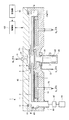
本発明の一実施形態に係る基板処理装置について説明する。図1は、本発明の一実施形態に係る基板処理装置の概略断面図である。図2は、本発明の一実施形態に係る基板処理装置の概略平面図である。図3は、本発明の一実施形態に係る基板処理装置における分離領域を説明するための一部断面図である。図4は、本発明の一実施形態に係る基板処理装置の他の断面を示す一部断面図である。
本発明の一実施形態に係る基板処理装置を用いた基板処理方法の一例について説明する。以下では、ウエハW上に形成された凹形状パターンの1つであるビア内にSiO2膜を形成する方法を例として説明する。なお、第1の反応ガスとしてSi含有ガス、第2の反応ガスとして酸化ガス、フッ素含有ガスとしてCF4とArガスとO2ガスとの混合ガス(以下「CF4/Ar/O2ガス」という。)を用いる場合を例として説明する。
次に、本発明の一実施形態に係る基板処理装置を用いて、シミュレーションと実験を行った。
2 回転テーブル
31、32 反応ガスノズル
90 活性化ガス供給部
93 シャワーヘッド部
93a ガス吐出孔
94 配管
96 水素含有ガス供給部
100 制御部
W ウエハ
Claims (9)
- 真空容器内に回転可能に設けられ、基板を載置可能な回転テーブルと、
前記回転テーブルの表面に第1の反応ガスを供給可能な第1の反応ガス供給部と、
前記第1の反応ガス供給部から前記回転テーブルの周方向に離間して設けられ、前記回転テーブルの表面に前記第1の反応ガスと反応する第2の反応ガスを供給可能な第2の反応ガス供給部と、
前記第1の反応ガス供給部及び前記第2の反応ガス供給部から前記回転テーブルの周方向に離間して設けられ、前記回転テーブルの表面に活性化されたフッ素含有ガスを供給可能な吐出部を含む活性化ガス供給部と
を備え、
前記活性化ガス供給部は、
前記吐出部よりも上流側に設けられ、前記吐出部に前記フッ素含有ガスを供給可能な配管と、
前記配管に設けられ、前記配管の内部に水素含有ガスを供給可能な1又は複数の水素含有ガス供給部と、
前記配管を介して前記吐出部と接続され、前記フッ素含有ガスを活性化するプラズマ生成部と、
を含み、
前記水素含有ガス供給部は、前記吐出部と前記プラズマ生成部との間に設けられている、
基板処理装置。 - 前記水素含有ガス供給部は、前記プラズマ生成部よりも前記吐出部に近い位置に設けられている、
請求項1に記載の基板処理装置。 - 前記第1の反応ガスはシリコン含有ガスであり、
前記第2の反応ガスは酸化ガスであり、
請求項1又は2に記載の基板処理装置。 - 前記活性化ガス供給部により前記回転テーブルの表面に供給される前記フッ素含有ガスの分布に基づいて、前記水素含有ガス供給部から供給される前記水素含有ガスの流量を制御する制御部を更に有する、
請求項1乃至3のいずれか一項に記載の基板処理装置。 - 前記制御部は、
前記基板の表面に成膜のみを行うときには、前記第1の反応ガス供給部及び前記第2の反応ガス供給部から前記第1の反応ガス及び前記第2の反応ガスを各々供給すると共に、前記活性化ガス供給部からの前記フッ素含有ガスの供給を停止し、
前記基板の表面に形成された膜のエッチングのみを行うときには、前記第1の反応ガス供給部及び前記第2の反応ガス供給部からの前記第1の反応ガス及び前記第2の反応ガスの供給を停止すると共に、前記活性化ガス供給部及び前記水素含有ガス供給部から前記フッ素含有ガス及び前記水素含有ガスを各々供給する、
請求項4に記載の基板処理装置。 - 真空容器内に設けられた回転テーブルの表面に基板を載置し、回転テーブルを回転させながらフッ素含有ガスを真空容器内に供給し、前記基板の表面に形成された膜をエッチングするエッチング工程を含む基板処理方法であって、
前記エッチング工程は、前記回転テーブルの表面にフッ素含有ガスを供給すると共に、前記フッ素含有ガスを前記回転テーブルの表面に供給するガス吐出孔を含む吐出部よりも上流側から水素含有ガスを供給する工程を含み、
前記回転テーブルの表面に供給される前記フッ素含有ガスの分布に基づいて、前記水素含有ガスの流量を変化させる、
基板処理方法。 - 前記回転テーブルを回転させながら、第1の反応ガスと、前記第1の反応ガスと反応する第2の反応ガスとを前記真空容器内に供給し、前記基板の表面に膜を形成する成膜工程を更に有する、
請求項6に記載の基板処理方法。 - 前記成膜工程は、前記回転テーブルを複数回連続的に回転させながら、前記フッ素含有ガスを前記真空容器内に供給することなく、前記第1の反応ガス及び前記第2の反応ガスを前記真空容器内に供給する工程を含み、
前記エッチング工程は、前記回転テーブルを複数回連続的に回転させながら、前記第1の反応ガス及び前記第2の反応ガスを前記真空容器内に供給することなく、前記フッ素含有ガス及び前記水素含有ガスを前記真空容器内に供給する工程を含む、
請求項7に記載の基板処理方法。 - 前記回転テーブルを複数回連続的に回転させながら、前記第1の反応ガス、前記第2の反応ガス、前記フッ素含有ガス及び前記水素含有ガスを前記真空容器内に同時に供給し、前記回転テーブルが1回転する間に、前記成膜工程と前記エッチング工程とを1回ずつ行うサイクルを複数回繰り返す、
請求項7に記載の基板処理方法。
Priority Applications (5)
| Application Number | Priority Date | Filing Date | Title |
|---|---|---|---|
| JP2015041499A JP6388552B2 (ja) | 2015-03-03 | 2015-03-03 | 基板処理装置及び基板処理方法 |
| US15/051,836 US10151034B2 (en) | 2015-03-03 | 2016-02-24 | Substrate processing method including supplying a fluorine-containing gas on a surface of a substrate |
| KR1020160023460A KR101989657B1 (ko) | 2015-03-03 | 2016-02-26 | 기판 처리 장치 및 기판 처리 방법 |
| TW105106058A TWI663673B (zh) | 2015-03-03 | 2016-03-01 | 基板處理裝置及基板處理方法(一) |
| CN201610119871.4A CN105937023B (zh) | 2015-03-03 | 2016-03-03 | 基板处理装置以及基板处理方法 |
Applications Claiming Priority (1)
| Application Number | Priority Date | Filing Date | Title |
|---|---|---|---|
| JP2015041499A JP6388552B2 (ja) | 2015-03-03 | 2015-03-03 | 基板処理装置及び基板処理方法 |
Publications (2)
| Publication Number | Publication Date |
|---|---|
| JP2016162930A JP2016162930A (ja) | 2016-09-05 |
| JP6388552B2 true JP6388552B2 (ja) | 2018-09-12 |
Family
ID=56845486
Family Applications (1)
| Application Number | Title | Priority Date | Filing Date |
|---|---|---|---|
| JP2015041499A Active JP6388552B2 (ja) | 2015-03-03 | 2015-03-03 | 基板処理装置及び基板処理方法 |
Country Status (5)
| Country | Link |
|---|---|
| US (1) | US10151034B2 (ja) |
| JP (1) | JP6388552B2 (ja) |
| KR (1) | KR101989657B1 (ja) |
| CN (1) | CN105937023B (ja) |
| TW (1) | TWI663673B (ja) |
Families Citing this family (9)
| Publication number | Priority date | Publication date | Assignee | Title |
|---|---|---|---|---|
| JP6804270B2 (ja) * | 2016-11-21 | 2020-12-23 | 東京エレクトロン株式会社 | 基板処理装置、および基板処理方法 |
| JP6869024B2 (ja) | 2016-12-20 | 2021-05-12 | 東京エレクトロン株式会社 | パーティクル除去方法及び基板処理方法 |
| CN108335978B (zh) * | 2017-01-20 | 2022-08-26 | 东京毅力科创株式会社 | 等离子体处理装置 |
| KR102096700B1 (ko) * | 2017-03-29 | 2020-04-02 | 도쿄엘렉트론가부시키가이샤 | 기판 처리 장치 및 기판 처리 방법 |
| JP7278123B2 (ja) * | 2019-03-22 | 2023-05-19 | 東京エレクトロン株式会社 | 処理方法 |
| US11817313B2 (en) * | 2020-02-05 | 2023-11-14 | Applied Materials, Inc. | Methods for pressure ramped plasma purge |
| CN116479399B (zh) * | 2022-01-13 | 2025-09-05 | 中国石油化工股份有限公司 | Cvd金刚石膜生长装置及方法 |
| CN120883347A (zh) * | 2023-03-15 | 2025-10-31 | 朗姆研究公司 | 用于前体输送的连接器 |
| JP2024152184A (ja) | 2023-04-14 | 2024-10-25 | 東京エレクトロン株式会社 | 基板処理方法及び基板処理装置 |
Family Cites Families (14)
| Publication number | Priority date | Publication date | Assignee | Title |
|---|---|---|---|---|
| JPS5751265A (en) * | 1980-09-10 | 1982-03-26 | Hitachi Ltd | Microwave plasma etching device |
| US6534409B1 (en) * | 1996-12-04 | 2003-03-18 | Micron Technology, Inc. | Silicon oxide co-deposition/etching process |
| US6451217B1 (en) * | 1998-06-09 | 2002-09-17 | Speedfam-Ipec Co., Ltd. | Wafer etching method |
| JP2003142484A (ja) | 2001-10-31 | 2003-05-16 | Mitsubishi Electric Corp | 半導体装置の製造方法 |
| JP2004179426A (ja) * | 2002-11-27 | 2004-06-24 | Tokyo Electron Ltd | 基板処理装置のクリーニング方法 |
| US20070218702A1 (en) * | 2006-03-15 | 2007-09-20 | Asm Japan K.K. | Semiconductor-processing apparatus with rotating susceptor |
| WO2008016836A2 (en) * | 2006-07-29 | 2008-02-07 | Lotus Applied Technology, Llc | Radical-enhanced atomic layer deposition system and method |
| US20080142483A1 (en) * | 2006-12-07 | 2008-06-19 | Applied Materials, Inc. | Multi-step dep-etch-dep high density plasma chemical vapor deposition processes for dielectric gapfills |
| JP5195174B2 (ja) | 2008-08-29 | 2013-05-08 | 東京エレクトロン株式会社 | 成膜装置及び成膜方法 |
| JP5599350B2 (ja) | 2011-03-29 | 2014-10-01 | 東京エレクトロン株式会社 | 成膜装置及び成膜方法 |
| US8809170B2 (en) * | 2011-05-19 | 2014-08-19 | Asm America Inc. | High throughput cyclical epitaxial deposition and etch process |
| WO2013146278A1 (ja) * | 2012-03-30 | 2013-10-03 | 株式会社日立国際電気 | 半導体装置の製造方法、基板処理方法及び基板処理装置 |
| SG2013083241A (en) | 2012-11-08 | 2014-06-27 | Novellus Systems Inc | Conformal film deposition for gapfill |
| JP6735549B2 (ja) * | 2015-11-04 | 2020-08-05 | 東京エレクトロン株式会社 | 基板処理装置、基板処理方法及びリング状部材 |
-
2015
- 2015-03-03 JP JP2015041499A patent/JP6388552B2/ja active Active
-
2016
- 2016-02-24 US US15/051,836 patent/US10151034B2/en active Active
- 2016-02-26 KR KR1020160023460A patent/KR101989657B1/ko active Active
- 2016-03-01 TW TW105106058A patent/TWI663673B/zh active
- 2016-03-03 CN CN201610119871.4A patent/CN105937023B/zh active Active
Also Published As
| Publication number | Publication date |
|---|---|
| US10151034B2 (en) | 2018-12-11 |
| CN105937023B (zh) | 2019-09-10 |
| JP2016162930A (ja) | 2016-09-05 |
| TWI663673B (zh) | 2019-06-21 |
| KR101989657B1 (ko) | 2019-06-14 |
| US20160258065A1 (en) | 2016-09-08 |
| CN105937023A (zh) | 2016-09-14 |
| KR20160107105A (ko) | 2016-09-13 |
| TW201705333A (zh) | 2017-02-01 |
Similar Documents
| Publication | Publication Date | Title |
|---|---|---|
| JP6388552B2 (ja) | 基板処理装置及び基板処理方法 | |
| JP6388553B2 (ja) | 基板処理装置及び基板処理方法 | |
| US9711370B2 (en) | Substrate processing apparatus and method of processing a substrate | |
| TWI820059B (zh) | 保護膜形成方法 | |
| JP6412466B2 (ja) | 基板処理装置及び基板処理方法 | |
| JP2018117038A (ja) | 保護膜形成方法 | |
| JP6869024B2 (ja) | パーティクル除去方法及び基板処理方法 | |
| TWI733809B (zh) | 成膜裝置 | |
| JP6735549B2 (ja) | 基板処理装置、基板処理方法及びリング状部材 | |
| CN110718461A (zh) | 成膜方法 | |
| KR20240153262A (ko) | 기판 처리 방법 및 기판 처리 장치 |
Legal Events
| Date | Code | Title | Description |
|---|---|---|---|
| A621 | Written request for application examination |
Free format text: JAPANESE INTERMEDIATE CODE: A621 Effective date: 20170815 |
|
| A977 | Report on retrieval |
Free format text: JAPANESE INTERMEDIATE CODE: A971007 Effective date: 20180528 |
|
| A131 | Notification of reasons for refusal |
Free format text: JAPANESE INTERMEDIATE CODE: A131 Effective date: 20180605 |
|
| A521 | Request for written amendment filed |
Free format text: JAPANESE INTERMEDIATE CODE: A523 Effective date: 20180713 |
|
| TRDD | Decision of grant or rejection written | ||
| A01 | Written decision to grant a patent or to grant a registration (utility model) |
Free format text: JAPANESE INTERMEDIATE CODE: A01 Effective date: 20180731 |
|
| A61 | First payment of annual fees (during grant procedure) |
Free format text: JAPANESE INTERMEDIATE CODE: A61 Effective date: 20180814 |
|
| R150 | Certificate of patent or registration of utility model |
Ref document number: 6388552 Country of ref document: JP Free format text: JAPANESE INTERMEDIATE CODE: R150 |
|
| R250 | Receipt of annual fees |
Free format text: JAPANESE INTERMEDIATE CODE: R250 |
|
| R250 | Receipt of annual fees |
Free format text: JAPANESE INTERMEDIATE CODE: R250 |
|
| R250 | Receipt of annual fees |
Free format text: JAPANESE INTERMEDIATE CODE: R250 |
|
| R250 | Receipt of annual fees |
Free format text: JAPANESE INTERMEDIATE CODE: R250 |
|
| R250 | Receipt of annual fees |
Free format text: JAPANESE INTERMEDIATE CODE: R250 |