JP6380204B2 - Halftone phase shift mask blank, halftone phase shift mask and pattern exposure method - Google Patents
Halftone phase shift mask blank, halftone phase shift mask and pattern exposure method Download PDFInfo
- Publication number
- JP6380204B2 JP6380204B2 JP2015073045A JP2015073045A JP6380204B2 JP 6380204 B2 JP6380204 B2 JP 6380204B2 JP 2015073045 A JP2015073045 A JP 2015073045A JP 2015073045 A JP2015073045 A JP 2015073045A JP 6380204 B2 JP6380204 B2 JP 6380204B2
- Authority
- JP
- Japan
- Prior art keywords
- phase shift
- silicon
- less
- halftone phase
- film
- Prior art date
- Legal status (The legal status is an assumption and is not a legal conclusion. Google has not performed a legal analysis and makes no representation as to the accuracy of the status listed.)
- Active
Links
Images
Classifications
-
- G—PHYSICS
- G03—PHOTOGRAPHY; CINEMATOGRAPHY; ANALOGOUS TECHNIQUES USING WAVES OTHER THAN OPTICAL WAVES; ELECTROGRAPHY; HOLOGRAPHY
- G03F—PHOTOMECHANICAL PRODUCTION OF TEXTURED OR PATTERNED SURFACES, e.g. FOR PRINTING, FOR PROCESSING OF SEMICONDUCTOR DEVICES; MATERIALS THEREFOR; ORIGINALS THEREFOR; APPARATUS SPECIALLY ADAPTED THEREFOR
- G03F1/00—Originals for photomechanical production of textured or patterned surfaces, e.g., masks, photo-masks, reticles; Mask blanks or pellicles therefor; Containers specially adapted therefor; Preparation thereof
- G03F1/26—Phase shift masks [PSM]; PSM blanks; Preparation thereof
- G03F1/28—Phase shift masks [PSM]; PSM blanks; Preparation thereof with three or more diverse phases on the same PSM; Preparation thereof
-
- G—PHYSICS
- G03—PHOTOGRAPHY; CINEMATOGRAPHY; ANALOGOUS TECHNIQUES USING WAVES OTHER THAN OPTICAL WAVES; ELECTROGRAPHY; HOLOGRAPHY
- G03F—PHOTOMECHANICAL PRODUCTION OF TEXTURED OR PATTERNED SURFACES, e.g. FOR PRINTING, FOR PROCESSING OF SEMICONDUCTOR DEVICES; MATERIALS THEREFOR; ORIGINALS THEREFOR; APPARATUS SPECIALLY ADAPTED THEREFOR
- G03F1/00—Originals for photomechanical production of textured or patterned surfaces, e.g., masks, photo-masks, reticles; Mask blanks or pellicles therefor; Containers specially adapted therefor; Preparation thereof
- G03F1/26—Phase shift masks [PSM]; PSM blanks; Preparation thereof
- G03F1/29—Rim PSM or outrigger PSM; Preparation thereof
-
- G—PHYSICS
- G03—PHOTOGRAPHY; CINEMATOGRAPHY; ANALOGOUS TECHNIQUES USING WAVES OTHER THAN OPTICAL WAVES; ELECTROGRAPHY; HOLOGRAPHY
- G03F—PHOTOMECHANICAL PRODUCTION OF TEXTURED OR PATTERNED SURFACES, e.g. FOR PRINTING, FOR PROCESSING OF SEMICONDUCTOR DEVICES; MATERIALS THEREFOR; ORIGINALS THEREFOR; APPARATUS SPECIALLY ADAPTED THEREFOR
- G03F1/00—Originals for photomechanical production of textured or patterned surfaces, e.g., masks, photo-masks, reticles; Mask blanks or pellicles therefor; Containers specially adapted therefor; Preparation thereof
- G03F1/26—Phase shift masks [PSM]; PSM blanks; Preparation thereof
- G03F1/32—Attenuating PSM [att-PSM], e.g. halftone PSM or PSM having semi-transparent phase shift portion; Preparation thereof
-
- G—PHYSICS
- G03—PHOTOGRAPHY; CINEMATOGRAPHY; ANALOGOUS TECHNIQUES USING WAVES OTHER THAN OPTICAL WAVES; ELECTROGRAPHY; HOLOGRAPHY
- G03F—PHOTOMECHANICAL PRODUCTION OF TEXTURED OR PATTERNED SURFACES, e.g. FOR PRINTING, FOR PROCESSING OF SEMICONDUCTOR DEVICES; MATERIALS THEREFOR; ORIGINALS THEREFOR; APPARATUS SPECIALLY ADAPTED THEREFOR
- G03F1/00—Originals for photomechanical production of textured or patterned surfaces, e.g., masks, photo-masks, reticles; Mask blanks or pellicles therefor; Containers specially adapted therefor; Preparation thereof
- G03F1/54—Absorbers, e.g. of opaque materials
- G03F1/56—Organic absorbers, e.g. of photo-resists
-
- G—PHYSICS
- G03—PHOTOGRAPHY; CINEMATOGRAPHY; ANALOGOUS TECHNIQUES USING WAVES OTHER THAN OPTICAL WAVES; ELECTROGRAPHY; HOLOGRAPHY
- G03F—PHOTOMECHANICAL PRODUCTION OF TEXTURED OR PATTERNED SURFACES, e.g. FOR PRINTING, FOR PROCESSING OF SEMICONDUCTOR DEVICES; MATERIALS THEREFOR; ORIGINALS THEREFOR; APPARATUS SPECIALLY ADAPTED THEREFOR
- G03F1/00—Originals for photomechanical production of textured or patterned surfaces, e.g., masks, photo-masks, reticles; Mask blanks or pellicles therefor; Containers specially adapted therefor; Preparation thereof
- G03F1/60—Substrates
-
- G—PHYSICS
- G03—PHOTOGRAPHY; CINEMATOGRAPHY; ANALOGOUS TECHNIQUES USING WAVES OTHER THAN OPTICAL WAVES; ELECTROGRAPHY; HOLOGRAPHY
- G03F—PHOTOMECHANICAL PRODUCTION OF TEXTURED OR PATTERNED SURFACES, e.g. FOR PRINTING, FOR PROCESSING OF SEMICONDUCTOR DEVICES; MATERIALS THEREFOR; ORIGINALS THEREFOR; APPARATUS SPECIALLY ADAPTED THEREFOR
- G03F1/00—Originals for photomechanical production of textured or patterned surfaces, e.g., masks, photo-masks, reticles; Mask blanks or pellicles therefor; Containers specially adapted therefor; Preparation thereof
- G03F1/68—Preparation processes not covered by groups G03F1/20 - G03F1/50
- G03F1/80—Etching
-
- G—PHYSICS
- G03—PHOTOGRAPHY; CINEMATOGRAPHY; ANALOGOUS TECHNIQUES USING WAVES OTHER THAN OPTICAL WAVES; ELECTROGRAPHY; HOLOGRAPHY
- G03F—PHOTOMECHANICAL PRODUCTION OF TEXTURED OR PATTERNED SURFACES, e.g. FOR PRINTING, FOR PROCESSING OF SEMICONDUCTOR DEVICES; MATERIALS THEREFOR; ORIGINALS THEREFOR; APPARATUS SPECIALLY ADAPTED THEREFOR
- G03F7/00—Photomechanical, e.g. photolithographic, production of textured or patterned surfaces, e.g. printing surfaces; Materials therefor, e.g. comprising photoresists; Apparatus specially adapted therefor
- G03F7/20—Exposure; Apparatus therefor
-
- G—PHYSICS
- G03—PHOTOGRAPHY; CINEMATOGRAPHY; ANALOGOUS TECHNIQUES USING WAVES OTHER THAN OPTICAL WAVES; ELECTROGRAPHY; HOLOGRAPHY
- G03F—PHOTOMECHANICAL PRODUCTION OF TEXTURED OR PATTERNED SURFACES, e.g. FOR PRINTING, FOR PROCESSING OF SEMICONDUCTOR DEVICES; MATERIALS THEREFOR; ORIGINALS THEREFOR; APPARATUS SPECIALLY ADAPTED THEREFOR
- G03F7/00—Photomechanical, e.g. photolithographic, production of textured or patterned surfaces, e.g. printing surfaces; Materials therefor, e.g. comprising photoresists; Apparatus specially adapted therefor
- G03F7/26—Processing photosensitive materials; Apparatus therefor
- G03F7/28—Processing photosensitive materials; Apparatus therefor for obtaining powder images
-
- G—PHYSICS
- G03—PHOTOGRAPHY; CINEMATOGRAPHY; ANALOGOUS TECHNIQUES USING WAVES OTHER THAN OPTICAL WAVES; ELECTROGRAPHY; HOLOGRAPHY
- G03F—PHOTOMECHANICAL PRODUCTION OF TEXTURED OR PATTERNED SURFACES, e.g. FOR PRINTING, FOR PROCESSING OF SEMICONDUCTOR DEVICES; MATERIALS THEREFOR; ORIGINALS THEREFOR; APPARATUS SPECIALLY ADAPTED THEREFOR
- G03F7/00—Photomechanical, e.g. photolithographic, production of textured or patterned surfaces, e.g. printing surfaces; Materials therefor, e.g. comprising photoresists; Apparatus specially adapted therefor
- G03F7/70—Microphotolithographic exposure; Apparatus therefor
- G03F7/70216—Mask projection systems
- G03F7/70283—Mask effects on the imaging process
-
- H—ELECTRICITY
- H01—ELECTRIC ELEMENTS
- H01L—SEMICONDUCTOR DEVICES NOT COVERED BY CLASS H10
- H01L21/00—Processes or apparatus adapted for the manufacture or treatment of semiconductor or solid state devices or of parts thereof
- H01L21/02—Manufacture or treatment of semiconductor devices or of parts thereof
- H01L21/027—Making masks on semiconductor bodies for further photolithographic processing not provided for in group H01L21/18 or H01L21/34
- H01L21/0271—Making masks on semiconductor bodies for further photolithographic processing not provided for in group H01L21/18 or H01L21/34 comprising organic layers
- H01L21/0273—Making masks on semiconductor bodies for further photolithographic processing not provided for in group H01L21/18 or H01L21/34 comprising organic layers characterised by the treatment of photoresist layers
- H01L21/0274—Photolithographic processes
-
- H—ELECTRICITY
- H01—ELECTRIC ELEMENTS
- H01L—SEMICONDUCTOR DEVICES NOT COVERED BY CLASS H10
- H01L21/00—Processes or apparatus adapted for the manufacture or treatment of semiconductor or solid state devices or of parts thereof
- H01L21/02—Manufacture or treatment of semiconductor devices or of parts thereof
- H01L21/027—Making masks on semiconductor bodies for further photolithographic processing not provided for in group H01L21/18 or H01L21/34
- H01L21/033—Making masks on semiconductor bodies for further photolithographic processing not provided for in group H01L21/18 or H01L21/34 comprising inorganic layers
- H01L21/0334—Making masks on semiconductor bodies for further photolithographic processing not provided for in group H01L21/18 or H01L21/34 comprising inorganic layers characterised by their size, orientation, disposition, behaviour, shape, in horizontal or vertical plane
- H01L21/0337—Making masks on semiconductor bodies for further photolithographic processing not provided for in group H01L21/18 or H01L21/34 comprising inorganic layers characterised by their size, orientation, disposition, behaviour, shape, in horizontal or vertical plane characterised by the process involved to create the mask, e.g. lift-off masks, sidewalls, or to modify the mask, e.g. pre-treatment, post-treatment
Description
本発明は、半導体集積回路などの製造などに用いられるハーフトーン位相シフトマスクブランク、ハーフトーン位相シフトマスク、及びハーフトーン位相シフトマスクを用いたパターン露光方法に関する。 The present invention relates to a halftone phase shift mask blank, a halftone phase shift mask, and a pattern exposure method using the halftone phase shift mask used for manufacturing a semiconductor integrated circuit or the like.
半導体技術の分野では、パターンの更なる微細化のための研究開発が進められている。特に近年では、大規模集積回路の高集積化に伴い、回路パターンの微細化や配線パターンの細線化、セルを構成する層間配線のためのコンタクトホールパターンの微細化などが進行し、微細加工技術への要求はますます高くなってきている。これに伴い、微細加工の際のフォトリソグラフィ工程で用いられるフォトマスクの製造技術の分野においても、より微細で、かつ正確な回路パターン(マスクパターン)を形成する技術の開発が求められるようになってきている。 In the field of semiconductor technology, research and development for further miniaturization of patterns is underway. In recent years, in particular, along with the high integration of large-scale integrated circuits, miniaturization of circuit patterns, thinning of wiring patterns, and miniaturization of contact hole patterns for interlayer wiring constituting cells have progressed. The demand for is getting higher and higher. As a result, in the field of manufacturing technology of photomasks used in photolithography processes during microfabrication, development of technology for forming finer and more accurate circuit patterns (mask patterns) has been required. It is coming.
一般に、フォトリソグラフィ技術により半導体基板上にパターンを形成する際には、縮小投影が行われる。このため、フォトマスクに形成されるパターンのサイズは、半導体基板上に形成されるパターンのサイズの4倍程度となる。今日のフォトリソグラフィ技術分野においては、描画される回路パターンのサイズは、露光で使用される光の波長をかなり下回るものとなっている。このため、回路パターンのサイズを単純に4倍にしてフォトマスクパターンを形成した場合には、露光の際に生じる光の干渉などの影響によって、半導体基板上のレジスト膜に本来の形状が転写されない結果となってしまう。 In general, reduction projection is performed when a pattern is formed on a semiconductor substrate by a photolithography technique. For this reason, the size of the pattern formed on the photomask is about four times the size of the pattern formed on the semiconductor substrate. In today's photolithography technology field, the size of a circuit pattern to be drawn is considerably less than the wavelength of light used for exposure. For this reason, when a photomask pattern is formed by simply quadrupling the size of the circuit pattern, the original shape is not transferred to the resist film on the semiconductor substrate due to the influence of light interference generated during exposure. Result.
そこで、フォトマスクに形成するパターンを、実際の回路パターンよりも複雑な形状とすることにより、上述の光の干渉などの影響を軽減する場合もある。このようなパターン形状としては、例えば、実際の回路パターンに光学近接効果補正(OPC: Optical Proximity Correction)を施した形状がある。また、パターンの微細化と高精度化に応えるべく、変形照明、液浸技術、解像度向上技術(RET: Resolution Enhancement Technology)、二重露光(ダブルパターニングリソグラフィ)などの技術も応用されている。 Therefore, there is a case where the effect of the above-described light interference or the like is reduced by making the pattern formed on the photomask more complicated than the actual circuit pattern. As such a pattern shape, for example, there is a shape in which an optical proximity effect correction (OPC: Optical Proximity Correction) is applied to an actual circuit pattern. In addition, in order to meet the miniaturization and high accuracy of patterns, technologies such as modified illumination, immersion technology, resolution enhancement technology (RET), double exposure (double patterning lithography) are also applied.
RETのひとつとして、位相シフト法が用いられている。位相シフト法はフォトマスク上に、位相を概ね180°反転させる膜のパターンを形成し、光の干渉を利用してコントラストを向上させる方法である。これを応用したフォトマスクのひとつとしてハーフトーン位相シフトマスクがある。ハーフトーン位相シフトマスクは、石英などの露光光に対して透明な基板の上に、位相を概ね180°反転させ、パターン形成に寄与しない程度の透過率を有するハーフトーン位相シフト膜のマスクパターンを形成したものである。ハーフトーン位相シフトマスクとしては、モリブテンシリサイド酸化物(MoSiO)、モリブテンシリサイド酸化窒化物(MoSiON)からなるハーフトーン位相シフト膜を有するものなどが提案されている(特開平7−140635号公報(特許文献1))。 As one of RET, a phase shift method is used. The phase shift method is a method in which a film pattern that inverts the phase by approximately 180 ° is formed on a photomask, and contrast is improved by utilizing light interference. One of the photomasks to which this is applied is a halftone phase shift mask. A halftone phase shift mask is a mask pattern of a halftone phase shift film on a substrate transparent to exposure light such as quartz, having a transmittance that does not contribute to pattern formation by inverting the phase by approximately 180 °. Formed. As a halftone phase shift mask, a mask having a halftone phase shift film made of molybdenum silicide oxide (MoSiO) or molybdenum silicide oxynitride (MoSiON) has been proposed (Japanese Patent Laid-Open No. 7-140635 (patent). Reference 1)).
また、フォトリソグラフィ技術により、より微細な像を得るために、露光光源に、より短波長のものが使われるようになり、現在の最先端の実用加工工程では、露光光源は、KrFエキシマレーザー光(248nm)からArFエキシマレーザー光(193nm)に移行している。ところが、より高エネルギーのArFエキシマレーザー光を使うことにより、KrFエキシマレーザー光では見られなかったマスクダメージが生じることが判明した。そのひとつが、フォトマスクを連続使用すると、フォトマスク上に異物状の成長欠陥が発生する問題である。この成長欠陥は、ヘイズと呼ばれ、原因は、当初は、マスクパターン表面における硫酸アンモニウム結晶の成長と考えられていたが、現在では、有機物が関与するものも考えられるようになってきている。 Also, in order to obtain a finer image by photolithography technology, an exposure light source having a shorter wavelength has been used. In the current state-of-the-art practical processing process, the exposure light source is a KrF excimer laser beam. It has shifted from (248 nm) to ArF excimer laser light (193 nm). However, it has been found that using higher energy ArF excimer laser light causes mask damage that was not seen with KrF excimer laser light. One of the problems is that when a photomask is continuously used, a foreign growth defect is generated on the photomask. This growth defect is called haze, and the cause was originally thought to be the growth of ammonium sulfate crystals on the surface of the mask pattern, but now it is also considered that organic matter is involved.
ヘイズの問題の対策として、例えば、特開2008−276002号公報(特許文献2)には、フォトマスクに対してArFエキシマレーザー光を長時間照射したときに発生する成長欠陥に対し、所定の段階でフォトマスクを洗浄することにより、フォトマスクの継続使用ができることが示されている。 As a countermeasure against the haze problem, for example, Japanese Patent Laid-Open No. 2008-276002 (Patent Document 2) discloses a predetermined stage for a growth defect that occurs when an ArF excimer laser beam is irradiated to a photomask for a long time. It is shown that the photomask can be used continuously by cleaning the photomask.
また、パターン転写におけるArFエキシマレーザー光の露光照射量の増加に伴い、ヘイズとは異なるダメージがフォトマスクに生じ、累積の照射エネルギー量に応じてマスクのパターン寸法が変化することが報告されている(Thomas Faure et al., “Characterization of binary mask and attenuated phase shift mask blanks for 32nm mask fabrication”, Proc. Of SPIE, vol. 7122, pp712209-1〜712209-12(非特許文献1))。これは、ArFエキシマレーザー光を長時間照射すると、累積照射エネルギー量が大きくなり、パターン材質の酸化物と考えられる物質による層が、膜パターンの外側に成長し、パターン幅が変化してしまう問題である。また、このダメージを受けたマスクは、前述のヘイズの除去に用いるアンモニア水/過酸化水素水による洗浄や、硫酸/過酸化水素水による洗浄では回復しないことが示されており、原因を全く別にすると考えられる。 Further, it has been reported that as the exposure dose of ArF excimer laser light in pattern transfer increases, damage different from haze occurs in the photomask, and the pattern size of the mask changes according to the cumulative amount of irradiation energy. (Thomas Faure et al., “Characterization of binary mask and attenuated phase shift mask blanks for 32 nm mask fabrication”, Proc. Of SPIE, vol. 7122, pp712209-1 to 712209-12 (Non-patent Document 1)). This is because, when ArF excimer laser light is irradiated for a long time, the cumulative irradiation energy amount increases, and a layer made of a material considered to be an oxide of the pattern material grows outside the film pattern, and the pattern width changes. It is. In addition, this damaged mask has been shown not to recover by cleaning with aqueous ammonia / hydrogen peroxide used to remove the above-mentioned haze, or cleaning with sulfuric acid / hydrogen peroxide. I think that.
更に、上記Thomas Faureらの報告(非特許文献1)によれば、回路のパターン露光において、焦点深度を伸ばすために有用なマスク技術であるハーフトーン位相シフトマスクでは、特に、上記ArFエキシマレーザー光の照射によるMoSi系材料膜などの遷移金属ケイ素系材料膜の変質を伴うパターン寸法変動による劣化(以下、パターン寸法変動劣化と呼ぶ)が大きいことが指摘されている。そこで、高価なフォトマスクを長時間使用するためには、ArFエキシマレーザー光の照射によるパターン寸法変動劣化への対処が必要となる。 Further, according to the report by Thomas Faure et al. (Non-Patent Document 1), in the halftone phase shift mask which is a mask technique useful for increasing the depth of focus in pattern exposure of a circuit, the ArF excimer laser beam is particularly useful. It has been pointed out that deterioration due to pattern dimension fluctuation (hereinafter referred to as pattern dimension fluctuation deterioration) accompanied by alteration of a transition metal silicon-based material film such as a MoSi-based material film due to irradiation is large. Therefore, in order to use an expensive photomask for a long time, it is necessary to cope with deterioration in pattern dimension variation caused by irradiation with ArF excimer laser light.
ArFエキシマレーザー光などの短波長光の照射によるパターン寸法変動劣化は、上記Thomas Faureらの報告(非特許文献1)で明らかにされているとおり、ドライエア雰囲気で光を照射した場合には生じにくいものであり、パターン寸法変動劣化を防止するための新たな対処として、ドライエア中で露光を行う方法が考えられる。しかし、ドライエア雰囲気による制御は、付加装置を必要とする他、静電気対策などが新たに必要となるため、コストアップにつながる。そこで、湿度の完全除去を行わない、常用の雰囲気(例えば、湿度50%程度)において、長時間の露光を可能とする必要がある。 Pattern dimension fluctuation deterioration due to irradiation with short wavelength light such as ArF excimer laser light is not likely to occur when light is irradiated in a dry air atmosphere, as is clarified in the report by Thomas Faure et al. Therefore, as a new measure for preventing deterioration of pattern dimension fluctuation, a method of performing exposure in dry air is conceivable. However, the control in the dry air atmosphere requires an additional device and additionally requires countermeasures against static electricity, leading to an increase in cost. Therefore, it is necessary to enable long-time exposure in a normal atmosphere (for example, about 50% humidity) where humidity is not completely removed.
また、ArFエキシマレーザー光を光源とするリソグラフィーに用いるフォトマスクでは、ハーフトーン位相シフト膜においては、従来、遷移金属ケイ素系材料が用いられ、通常、モリブデンを含有するケイ素系材料が用いられている。この遷移金属ケイ素系材料の主たる構成元素は、遷移金属とケイ素であり、更に、軽元素として窒素及び/又は酸素を含有するもの(例えば、特開平7−140635号公報(特許文献1))がある。遷移金属としては、モリブデン、ジルコニウム、タンタル、タングステン、チタンなどが用いられ、特に、モリブデンが一般的に用いられる(例えば、特開平7−140635号公報(特許文献1))が、更に、第2の遷移金属が加えられる場合もある(特開2004−133029号公報(特許文献3))。また、遮光膜においても、遷移金属ケイ素系材料が用いられ、通常、モリブデンを含有するケイ素系材料が用いられる。しかし、このような遷移金属ケイ素系材料を用いたフォトマスクに高エネルギー光を多量に照射した場合、高エネルギー光の照射によるパターン寸法変動劣化が大きく、フォトマスクの使用寿命が、要求されるものより短くなってしまう。 In addition, in a photomask used for lithography using ArF excimer laser light as a light source, a transition metal silicon-based material is conventionally used in the halftone phase shift film, and a silicon-based material containing molybdenum is usually used. . The main constituent elements of this transition metal silicon-based material are transition metal and silicon, and further, those containing nitrogen and / or oxygen as light elements (for example, JP-A-7-140635 (Patent Document 1)). is there. As the transition metal, molybdenum, zirconium, tantalum, tungsten, titanium, or the like is used. In particular, molybdenum is generally used (for example, JP-A-7-140635 (Patent Document 1)). In some cases, a transition metal is added (Japanese Patent Laid-Open No. 2004-133029 (Patent Document 3)). In addition, a transition metal silicon-based material is also used for the light shielding film, and a silicon-based material containing molybdenum is usually used. However, when a large amount of high-energy light is irradiated onto a photomask using such a transition metal silicon-based material, the deterioration of pattern dimension variation due to irradiation with high-energy light is large, and the service life of the photomask is required. It will be shorter.
ArFエキシマレーザー光などの短波長光が、ハーフトーン位相シフトマスクのフォトマスクパターンに照射されることにより、露光に用いるフォトマスクパターンの線幅が変化してしまうパターン寸法変動劣化は重大な問題である。パターン幅の許容限界は、フォトマスクパターンの種類、特に適用されるパターンルールによって異なる。また、多少の変動であれば、露光条件を補正し、露光装置の照射条件を再設定して使用できる場合もあるものの、例えば、22nmのパターンルールによる半導体回路を形成するための露光では、フォトマスクパターン線幅の変動は概ね±5nm以下とする必要がある。しかし、パターン幅の変化量が大きい場合には、その変化量がフォトマスクの面内で分布を有する可能性がある。また、更なる微細化により、マスク上で100nm以下の極めて微細な補助パターンも形成される。そのため、これらマスク上でのパターン微細化と、マスクパターンの複雑化によるマスク加工コストの増加からも、パターン寸法変動劣化が極めて小さく、繰返し露光することができるハーフトーン位相シフトマスク膜が必要とされる。 Deterioration of pattern dimension variation that changes the line width of the photomask pattern used for exposure due to irradiation of the photomask pattern of the halftone phase shift mask with short wavelength light such as ArF excimer laser light is a serious problem. is there. The permissible limit of the pattern width varies depending on the type of photomask pattern, particularly the applied pattern rule. In addition, if there are some fluctuations, the exposure conditions may be corrected and the irradiation conditions of the exposure apparatus may be reset and used. However, in the exposure for forming a semiconductor circuit with a 22 nm pattern rule, for example, The variation of the mask pattern line width needs to be approximately ± 5 nm or less. However, when the change amount of the pattern width is large, there is a possibility that the change amount has a distribution in the plane of the photomask. Further, by further miniaturization, an extremely fine auxiliary pattern of 100 nm or less is formed on the mask. For this reason, a halftone phase shift mask film that can be repeatedly exposed is required because the pattern dimension variation deterioration is extremely small due to pattern miniaturization on these masks and an increase in mask processing cost due to complicated mask patterns. The
位相シフト膜は、薄い方が、パターン形成に有利であるだけでなく、三次元効果を低減することができるため有利である。そのため、フォトリソグラフィにおいて、より微細なパターンを形成するためには、更に薄い膜が求められる。 A thinner phase shift film is advantageous not only for pattern formation but also for reducing three-dimensional effects. Therefore, a thinner film is required in order to form a finer pattern in photolithography.
ハーフトーン位相シフトマスクブランクをハーフトーン位相シフトマスクの製造プロセスで使用する際、ハーフトーン位相シフトマスクブランク上に異物が存在すると、異物がパターン欠陥の原因となるため、このような異物を除去するために、ハーフトーン位相シフトマスクブランクは、ハーフトーン位相シフトマスク製造過程において何度も洗浄される。更に、ハーフトーン位相シフトマスクをフォトリソグラフィ工程で使用する際、製造されたハーフトーン位相シフトマスクそのものにパターン欠陥がなくても、フォトリソグラフィ工程中に、ハーフトーン位相シフトマスクに異物が付着すると、これを用いてパターニングされた半導体基板には、パターン転写不良が生じるため、ハーフトーン位相シフトマスクもまた繰り返し洗浄される。 When using a halftone phase shift mask blank in the halftone phase shift mask manufacturing process, if foreign matter is present on the halftone phase shift mask blank, the foreign matter will cause pattern defects. Therefore, the halftone phase shift mask blank is cleaned many times during the halftone phase shift mask manufacturing process. Furthermore, when the halftone phase shift mask is used in the photolithography process, even if there is no pattern defect in the manufactured halftone phase shift mask itself, foreign matters adhere to the halftone phase shift mask during the photolithography process. Since a pattern transfer defect occurs in the semiconductor substrate patterned using this, the halftone phase shift mask is also repeatedly cleaned.
ハーフトーン位相シフトマスクブランクやハーフトーン位相シフトマスクの異物除去のためには、ほとんどの場合、硫酸過水やオゾン水、アンモニア過水などによる化学的な洗浄が施される。ここで、硫酸過水は、硫酸と過酸化水素水を混合して得られる強力な酸化作用をもった洗浄剤であり、オゾン水はオゾンを水に溶け込ませたものであり、硫酸過水の代替として用いられる。特に、アンモニア過水は、アンモニア水と過酸化水素水を混合して得られる洗浄剤で、表面に付着した有機系異物がアンモニア過水に浸漬されると、アンモニアの溶解作用と過酸化水素の酸化作用により表面から有機系異物が離脱して分離されることで洗浄される。 In order to remove foreign matter from the halftone phase shift mask blank or the halftone phase shift mask, in most cases, chemical cleaning with sulfuric acid / hydrogen peroxide, ozone water, ammonia water, or the like is performed. Here, sulfuric acid / hydrogen peroxide is a cleaning agent having a strong oxidizing action obtained by mixing sulfuric acid and hydrogen peroxide water, and ozone water is a solution in which ozone is dissolved in water. Used as an alternative. In particular, ammonia perwater is a cleaning agent obtained by mixing ammonia water and hydrogen peroxide water. When organic foreign matter adhering to the surface is immersed in ammonia perwater, the ammonia dissolving action and the hydrogen peroxide Cleaning is performed by separating and separating organic foreign matters from the surface by the oxidative action.
このような薬液による化学的洗浄は、ハーフトーン位相シフトマスクブランクやハーフトーン位相シフトマスクに付着したパーティクルや汚染物といった異物を除去するために必要である一方で、ハーフトーン位相シフトマスクブランクやハーフトーン位相シフトマスクが備えるハーフトーン位相シフト膜にダメージを与えるおそれがある。例えば、上述したような化学的洗浄によってハーフトーン位相シフト膜の表面が変質してしまい、本来備えているはずの光学特性が変化してしまう可能性があり、ハーフトーン位相シフトマスクブランクやハーフトーン位相シフトマスクの化学的洗浄は、繰り返し施されるものであるから、各洗浄工程で生じるハーフトーン位相シフト膜の特性変化(例えば、位相差変化)は、可能な限り低く抑えられることが必要である。 Such chemical cleaning with a chemical solution is necessary to remove foreign substances such as particles and contaminants attached to the halftone phase shift mask blank and the halftone phase shift mask. There is a possibility of damaging the halftone phase shift film provided in the tone phase shift mask. For example, the surface of the halftone phase shift film may be altered by the chemical cleaning as described above, and the optical characteristics that should originally be provided may change. Since chemical cleaning of the phase shift mask is performed repeatedly, it is necessary to suppress the characteristic change (for example, phase difference change) of the halftone phase shift film generated in each cleaning process as low as possible. is there.
本発明は、上記課題を解決するためになされたものであり、パターンの微細化に対応できるハーフトーン位相シフト膜として、必要な位相差及び透過率を確保した上で、パターン形成や、三次元効果の低減などにおいて有利な、膜厚が薄いハーフトーン位相シフト膜であり、かつ化学的洗浄に対する耐薬品性に優れたハーフトーン位相シフト膜を有するハーフトーン位相シフトマスクブランク及びハーフトーン位相シフトマスク、並びにハーフトーン位相シフトマスクを用いたパターン露光方法を提供することを目的とする。 The present invention has been made in order to solve the above problems, and as a halftone phase shift film that can cope with pattern miniaturization, while ensuring necessary phase difference and transmittance, pattern formation and three-dimensional Halftone phase shift mask blank and halftone phase shift mask having a halftone phase shift film having a thin film thickness and excellent chemical resistance against chemical cleaning, which is advantageous in reducing effects, etc. An object of the present invention is to provide a pattern exposure method using a halftone phase shift mask.
本発明者らは、ハーフトーン位相シフト膜として必要な位相差と透過率とを確保した上で、膜厚が薄く、耐薬品性に優れたハーフトーン位相シフト膜の開発を目指し、まず、ハーフトーン位相シフト膜として常用されているモリブデンなどの遷移金属を含むハーフトーン位相シフト膜について検討した。しかし、ハーフトーン位相シフト膜では、遷移金属や酸素を添加すると、添加量に応じて、所定の透過率での膜の屈折率が下がってしまい、位相シフト膜として必要な位相差を確保するためには膜を厚くする必要があり、更に、耐薬品性も悪くなることがわかった。 The inventors of the present invention aimed to develop a halftone phase shift film having a thin film thickness and excellent chemical resistance while ensuring the necessary phase difference and transmittance as a halftone phase shift film. A halftone phase shift film containing a transition metal such as molybdenum, which is commonly used as a tone phase shift film, was studied. However, in the case of a halftone phase shift film, when a transition metal or oxygen is added, the refractive index of the film at a predetermined transmittance decreases depending on the amount added, so that the phase difference necessary for the phase shift film is secured. It is necessary to increase the thickness of the film, and the chemical resistance is also deteriorated.
そこで、本発明者らは、上記課題を解決するために、遷移金属の含有を極力抑えたハーフトーン位相シフト膜について鋭意検討を重ねた結果、ハーフトーン位相シフト膜を、ケイ素及び窒素からなるケイ素系材料、又はケイ素、窒素及び酸素からなり、酸素の含有率が6原子%以下のケイ素系材料で構成され、屈折率nが2.4以上、消衰係数kが0.4以上0.7以下の単層、又はケイ素及び窒素からなるケイ素系材料、又はケイ素、窒素及び酸素からなり、酸素の含有率が6原子%以下のケイ素系材料で構成され、屈折率nが2.4以上、消衰係数kが0.4以上0.7以下の層を1層以上含む多層で形成することにより、膜厚を67nm以下として、波長200nm以下の光に対し、位相差が150〜200°、透過率が3%以上12%以下であるハーフトーン位相シフト膜を形成できることを見出した。 Therefore, in order to solve the above-mentioned problems, the present inventors have made extensive studies on a halftone phase shift film in which the transition metal content is suppressed as much as possible. As a result, the halftone phase shift film is formed of silicon and silicon. Or a silicon-based material composed of silicon, nitrogen and oxygen and having an oxygen content of 6 atomic% or less, a refractive index n of 2.4 or more, and an extinction coefficient k of 0.4 or more and 0.7 The following monolayer, or a silicon-based material composed of silicon and nitrogen, or a silicon-based material composed of silicon, nitrogen and oxygen and having an oxygen content of 6 atomic% or less, and a refractive index n of 2.4 or more, By forming a multilayer including one or more layers having an extinction coefficient k of 0.4 or more and 0.7 or less, the film thickness is 67 nm or less, and the phase difference is 150 to 200 ° with respect to light having a wavelength of 200 nm or less. Transmittance is 3% or more 12 It found that to form a halftone phase shift film or less.
そして、このようなハーフトーン位相シフト膜が、化学的洗浄に対する耐薬品性に優れていること、また、ハーフトーン位相シフト膜をこのように構成することにより、ハーフトーン位相シフト膜のパターンを有するハーフトーン位相シフトマスクを用い、シリコンウエーハなどの被加工基板の上に、波長200nm以下の露光光で、ハーフピッチ50nm以下の被転写パターンを形成するためのフォトリソグラフィにおいて必要な、幅が100〜200nm程度のメインフォトマスクパターンを有するハーフトーン位相シフト膜パターンを有利に加工できるハーフトーン位相シフトマスクブランクが得られることを見出し、本発明をなすに至った。 Such a halftone phase shift film is excellent in chemical resistance against chemical cleaning, and has a halftone phase shift film pattern by configuring the halftone phase shift film in this way. Using a halftone phase shift mask, the width required for photolithography for forming a transferred pattern having a half pitch of 50 nm or less on exposure light having a wavelength of 200 nm or less on a workpiece substrate such as a silicon wafer is 100 to 100 mm. It has been found that a halftone phase shift mask blank capable of advantageously processing a halftone phase shift film pattern having a main photomask pattern of about 200 nm can be obtained, and the present invention has been made.
従って、本発明は、以下のハーフトーン位相シフトマスクブランク、ハーフトーン位相シフトマスク及びパターン露光方法を提供する。
請求項1:
透明基板上に、波長200nm以下の光で、位相シフト量が150〜200°、かつ透過率が3%以上12%以下であるハーフトーン位相シフト膜を有するハーフトーン位相シフトマスクブランクであって、
上記ハーフトーン位相シフト膜が、
ケイ素及び窒素からなるケイ素系材料、又はケイ素、窒素及び酸素からなり、該酸素の含有率が6原子%以下のケイ素系材料で構成され、屈折率nが2.4以上、消衰係数kが0.4以上0.7以下の単層で形成され、
膜厚が67nm以下であることを特徴とするハーフトーン位相シフトマスクブランク。
請求項2:
透明基板上に、波長200nm以下の光で、位相シフト量が150〜200°、かつ透過率が3%以上12%以下であるハーフトーン位相シフト膜を有するハーフトーン位相シフトマスクブランクであって、
上記ハーフトーン位相シフト膜が、
ケイ素及び窒素からなるケイ素系材料、又はケイ素、窒素及び酸素からなり、該酸素の含有率が6原子%以下のケイ素系材料で構成され、屈折率nが2.4以上、消衰係数kが0.4以上0.7以下の単層、又は
ケイ素及び窒素からなるケイ素系材料、又はケイ素、窒素及び酸素からなり、該酸素の含有率が6原子%以下のケイ素系材料で構成され、屈折率nが2.4以上、消衰係数kが0.4以上0.7以下の層を1層以上含む多層で形成され、
膜厚が67nm以下であり、
被加工基板にハーフピッチ50nm以下のパターンを形成するためのフォトリソグラフィにおいて、被加工基板上に形成したフォトレジスト膜に、波長200nm以下の露光光で上記パターンを転写するパターン露光に用いるハーフトーン位相シフトマスク用であることを特徴とするハーフトーン位相シフトマスクブランク。
請求項3:
透明基板上に、波長200nm以下の光で、位相シフト量が150〜200°、かつ透過率が3%以上12%以下であるハーフトーン位相シフト膜のパターンを有するハーフトーン位相シフトマスクであって、
上記ハーフトーン位相シフト膜が、
ケイ素及び窒素からなるケイ素系材料、又はケイ素、窒素及び酸素からなり、該酸素の含有率が6原子%以下のケイ素系材料で構成され、屈折率nが2.4以上、消衰係数kが0.4以上0.7以下の単層で形成され、
膜厚が67nm以下であることを特徴とするハーフトーン位相シフトマスク。
請求項4:
透明基板上に、波長200nm以下の光で、位相シフト量が150〜200°、かつ透過率が3%以上12%以下であるハーフトーン位相シフト膜のパターンを有するハーフトーン位相シフトマスクであって、
上記ハーフトーン位相シフト膜が、
ケイ素及び窒素からなるケイ素系材料、又はケイ素、窒素及び酸素からなり、該酸素の含有率が6原子%以下のケイ素系材料で構成され、屈折率nが2.4以上、消衰係数kが0.4以上0.7以下の単層、又は
ケイ素及び窒素からなるケイ素系材料、又はケイ素、窒素及び酸素からなり、該酸素の含有率が6原子%以下のケイ素系材料で構成され、屈折率nが2.4以上、消衰係数kが0.4以上0.7以下の層を1層以上含む多層で形成され、
膜厚が67nm以下であり、
被加工基板にハーフピッチ50nm以下のパターンを形成するためのフォトリソグラフィにおいて、被加工基板上に形成したフォトレジスト膜に、波長200nm以下の露光光で上記パターンを転写するパターン露光用であることを特徴とするハーフトーン位相シフトマスク。
請求項5:
被加工基板にハーフピッチ50nm以下のパターンを形成するためのフォトリソグラフィにおいて、被加工基板上に形成したフォトレジスト膜に、波長200nm以下の露光光で上記パターンを転写するパターン露光方法であって、
透明基板上に、波長200nm以下の光で、位相シフト量が150〜200°、かつ透過率が3%以上12%以下であるハーフトーン位相シフト膜のパターンを有し、
上記ハーフトーン位相シフト膜が、
ケイ素及び窒素からなるケイ素系材料、又はケイ素、窒素及び酸素からなり、該酸素の含有率が6原子%以下のケイ素系材料で構成され、屈折率nが2.4以上、消衰係数kが0.4以上0.7以下の単層、又は
ケイ素及び窒素からなるケイ素系材料、又はケイ素、窒素及び酸素からなり、該酸素の含有率が6原子%以下のケイ素系材料で構成され、屈折率nが2.4以上、消衰係数kが0.4以上0.7以下の層を1層以上含む多層で形成され、
膜厚が67nm以下であるハーフトーン位相シフトマスクを用いることを特徴とするパターン露光方法。
請求項6:
上記ハーフトーン位相シフト膜が、上記ケイ素及び窒素からなるケイ素系材料で構成された単層で形成されていることを特徴とする請求項5記載のパターン露光方法。
請求項7:
上記ハーフトーン位相シフト膜が、上記ケイ素及び窒素からなるケイ素系材料で構成された層を1層以上と、上記ケイ素、窒素及び酸素からなる層を1層以上とを含む多層で形成されていることを特徴とする請求項5記載のパターン露光方法。
Accordingly, the present invention provides the following halftone phase shift mask blank, halftone phase shift mask and pattern exposure method.
Claim 1:
A halftone phase shift mask blank having a halftone phase shift film on a transparent substrate having a wavelength of 200 nm or less, a phase shift amount of 150 to 200 °, and a transmittance of 3% or more and 12% or less,
The halftone phase shift film is
A silicon-based material composed of silicon and nitrogen, or a silicon-based material composed of silicon, nitrogen and oxygen and having an oxygen content of 6 atomic% or less, a refractive index n of 2.4 or more, and an extinction coefficient k. Formed with a single layer of 0.4 or more and 0.7 or less,
A halftone phase shift mask blank having a film thickness of 67 nm or less.
Claim 2 :
A halftone phase shift mask blank having a halftone phase shift film on a transparent substrate having a wavelength of 200 nm or less, a phase shift amount of 150 to 200 °, and a transmittance of 3% or more and 12% or less,
The halftone phase shift film is
A silicon-based material composed of silicon and nitrogen, or a silicon-based material composed of silicon, nitrogen and oxygen and having an oxygen content of 6 atomic% or less, a refractive index n of 2.4 or more, and an extinction coefficient k. 0.4 to 0.7 single layer, or
A silicon-based material composed of silicon and nitrogen, or a silicon-based material composed of silicon, nitrogen and oxygen and having an oxygen content of 6 atomic% or less, a refractive index n of 2.4 or more, and an extinction coefficient k. Formed of multiple layers including one or more layers of 0.4 or more and 0.7 or less,
The film thickness is 67 nm or less,
In photolithography for forming a pattern with a half pitch of 50 nm or less on a substrate to be processed, a halftone phase used for pattern exposure in which the pattern is transferred to a photoresist film formed on the substrate to be processed with exposure light having a wavelength of 200 nm or less. features and to Ruha Futon phase shift mask blank that is for shifting mask.
Claim 3 :
A halftone phase shift mask having a pattern of a halftone phase shift film having a phase shift amount of 150 to 200 ° and a transmittance of 3% or more and 12% or less with light having a wavelength of 200 nm or less on a transparent substrate. ,
The halftone phase shift film is
A silicon-based material composed of silicon and nitrogen, or a silicon-based material composed of silicon, nitrogen and oxygen and having an oxygen content of 6 atomic% or less, a refractive index n of 2.4 or more, and an extinction coefficient k. Formed with a single layer of 0.4 or more and 0.7 or less,
A halftone phase shift mask having a film thickness of 67 nm or less.
Claim 4 :
A halftone phase shift mask having a pattern of a halftone phase shift film having a phase shift amount of 150 to 200 ° and a transmittance of 3% or more and 12% or less with light having a wavelength of 200 nm or less on a transparent substrate. ,
The halftone phase shift film is
A silicon-based material composed of silicon and nitrogen, or a silicon-based material composed of silicon, nitrogen and oxygen and having an oxygen content of 6 atomic% or less, a refractive index n of 2.4 or more, and an extinction coefficient k. 0.4 to 0.7 single layer, or
A silicon-based material composed of silicon and nitrogen, or a silicon-based material composed of silicon, nitrogen and oxygen and having an oxygen content of 6 atomic% or less, a refractive index n of 2.4 or more, and an extinction coefficient k. Formed of multiple layers including one or more layers of 0.4 or more and 0.7 or less,
The film thickness is 67 nm or less,
In photolithography for forming a pattern with a half pitch of 50 nm or less on a substrate to be processed, it is for pattern exposure that transfers the pattern to the photoresist film formed on the substrate to be processed with exposure light having a wavelength of 200 nm or less. features and be Ruha Futon phase shift mask.
Claim 5 :
In photolithography for forming a pattern with a half pitch of 50 nm or less on a substrate to be processed, a pattern exposure method for transferring the pattern to a photoresist film formed on the substrate to be processed with exposure light having a wavelength of 200 nm or less,
On a transparent substrate, it has a pattern of a halftone phase shift film having a phase shift amount of 150 to 200 ° and a transmittance of 3% or more and 12% or less with light having a wavelength of 200 nm or less,
The halftone phase shift film is
A silicon-based material composed of silicon and nitrogen, or a silicon-based material composed of silicon, nitrogen and oxygen and having an oxygen content of 6 atomic% or less, a refractive index n of 2.4 or more, and an extinction coefficient k. A single layer of 0.4 or more and 0.7 or less, or a silicon-based material composed of silicon and nitrogen, or a silicon-based material composed of silicon, nitrogen and oxygen, the oxygen content of which is 6 atomic% or less, and is refracted. Formed of a multilayer including one or more layers having a rate n of 2.4 or more and an extinction coefficient k of 0.4 or more and 0.7 or less,
A pattern exposure method using a halftone phase shift mask having a film thickness of 67 nm or less.
Claim 6 :
6. The pattern exposure method according to claim 5 , wherein the halftone phase shift film is formed of a single layer made of a silicon-based material composed of silicon and nitrogen.
Claim 7 :
The halftone phase shift film is formed of a multilayer including one or more layers composed of the silicon-based material composed of silicon and nitrogen and one or more layers composed of the silicon, nitrogen and oxygen. 6. The pattern exposure method according to claim 5, wherein:
本発明によれば、フォトマスクパターンの加工において有利な、より薄いハーフトーン位相シフト膜であり、かつ化学的洗浄に対する耐薬品性にも優れたハーフトーン位相シフト膜であって、位相シフト膜として必要な位相差と、ハーフトーン膜として必要な透過率とが確保されたハーフトーン位相シフト膜を備えるハーフトーン位相シフトマスクブランク及びハーフトーン位相シフトマスクを提供できる。本発明のハーフトーン位相シフトマスクによれば、フォトリソグラフィにおける更なるパターンの微細化と高精度化の要求に適合した露光が可能である。 According to the present invention, a halftone phase shift film that is advantageous in photomask pattern processing, is a thinner halftone phase shift film, and is excellent in chemical resistance against chemical cleaning. A halftone phase shift mask blank and a halftone phase shift mask provided with a halftone phase shift film in which a necessary phase difference and a transmittance necessary as a halftone film are ensured can be provided. According to the halftone phase shift mask of the present invention, it is possible to perform exposure that meets the requirements for further pattern miniaturization and higher precision in photolithography.
以下、本発明について更に詳しく説明する。
本発明のハーフトーン位相シフトマスクブランク(ハーフトーン位相シフト型フォトマスクブランク)は、石英基板などの透明基板上に形成された単層、又は多層(即ち、2層以上)からなるハーフトーン位相シフト膜を有する。本発明において、透明基板は、例えば、SEMI規格において規定されている、6インチ角、厚さ25ミリインチの6025基板と呼ばれる透明基板が好適であり、SI単位系を用いた場合、通常、152mm角、厚さ6.35mmの透明基板と表記される。また、本発明のハーフトーン位相シフトマスク(ハーフトーン位相シフト型フォトマスク)は、ハーフトーン位相シフト膜のマスクパターン(フォトマスクパターン)を有する。
Hereinafter, the present invention will be described in more detail.
The halftone phase shift mask blank (halftone phase shift type photomask blank) of the present invention is a halftone phase shift composed of a single layer or multiple layers (that is, two or more layers) formed on a transparent substrate such as a quartz substrate. Has a membrane. In the present invention, the transparent substrate is preferably a transparent substrate called a 6025 substrate having a 6-inch square and a thickness of 25 millimeters, which is defined in the SEMI standard. When an SI unit system is used, it is usually a 152 mm square. And a transparent substrate having a thickness of 6.35 mm. The halftone phase shift mask (halftone phase shift type photomask) of the present invention has a mask pattern (photomask pattern) of a halftone phase shift film.
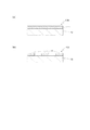
図1(A)は、本発明のハーフトーン位相シフトマスクブランクの一例を示す断面図であり、このハーフトーン位相シフトマスクブランク100は、透明基板10と、透明基板10上に形成されたハーフトーン位相シフト膜1とを備える。また、図1(B)は、本発明のハーフトーン位相シフトマスクの一例を示す断面図であり、このハーフトーン位相シフトマスク101は、透明基板10と、透明基板10上に形成されたハーフトーン位相シフト膜パターン11とを備える。
FIG. 1A is a cross-sectional view showing an example of the halftone phase shift mask blank of the present invention. The halftone phase shift mask blank 100 includes a
ハーフトーン位相シフト膜は、ハーフトーン位相シフト膜として必要な位相差及び透過率を満たすように、単層で構成してもよいが、例えば、所定の表面反射率を満たすようにするために、反射防止機能性を有する層を含むようにし、全体としてハーフトーン位相シフト膜として必要な位相差及び透過率を満たすように、多層で構成することも好適である。 The halftone phase shift film may be composed of a single layer so as to satisfy the phase difference and transmittance required as a halftone phase shift film.For example, in order to satisfy a predetermined surface reflectance, It is also preferable to include a layer having an antireflection function and to have a multilayer structure so as to satisfy the phase difference and transmittance required as a halftone phase shift film as a whole.
単層及び多層のいずれの場合においても、各々の層は、組成が厚さ方向に連続的に変化するように形成してもよい。また、ハーフトーン位相シフト膜を多層で構成する場合、構成元素が異なる層及び構成元素が同一で組成比が異なる層から選ばれる2層以上の組み合わせとしてよく、多層を3層以上で構成する場合は、隣接する層としなければ、同じ層を組み合わせることもできる。 In either case of a single layer or a multilayer, each layer may be formed such that the composition continuously changes in the thickness direction. Further, when the halftone phase shift film is composed of multiple layers, it may be a combination of two or more layers selected from layers having different constituent elements and layers having the same constituent elements but different composition ratios. When the multilayer is composed of three or more layers If they are not adjacent layers, the same layers can be combined.
本発明のハーフトーン位相シフト膜は、所定の膜厚において、波長200nm以下の光、特に、ハーフトーン位相シフトマスクを用いたフォトリソグラフィにおいて用いられるArFエキシマレーザー光(波長193nm)の露光光に対して、所定の位相シフト量(位相差)と、所定の透過率とを与える膜である。 The halftone phase shift film of the present invention has a predetermined film thickness with respect to light having a wavelength of 200 nm or less, particularly exposure light of ArF excimer laser light (wavelength 193 nm) used in photolithography using a halftone phase shift mask. Thus, the film provides a predetermined phase shift amount (phase difference) and a predetermined transmittance.
本発明のハーフトーン位相シフト膜の全体の厚さは、薄いほど微細なパターンを形成しやすいため67nm以下とすることが好ましく、より好ましくは65nm以下、更に好ましくは62nm以下である。一方、ハーフトーン位相シフト膜の膜厚の下限は、露光波長である波長200nm以下の光に対し、必要な光学特性が得られる範囲で設定され、特に制約はないが、一般的には40nm以上となる。 The total thickness of the halftone phase shift film of the present invention is preferably 67 nm or less, more preferably 65 nm or less, and still more preferably 62 nm or less, because the thinner the easier it is to form a fine pattern. On the other hand, the lower limit of the film thickness of the halftone phase shift film is set in a range in which necessary optical characteristics can be obtained with respect to light having a wavelength of 200 nm or less, which is an exposure wavelength. It becomes.
本発明のハーフトーン位相シフト膜の露光光に対する位相差は、ハーフトーン位相シフト膜が存在する部分(ハーフトーン位相シフト部)と、ハーフトーン位相シフト膜が存在しない部分との境界部において、それぞれを通過する露光光の位相差によって露光光が干渉して、コントラストを増大させることができる位相差であればよく、位相差は150〜200°であればよい。一般的なハーフトーン位相シフト膜では、位相差を略180°に設定するが、上述したコントラスト増大の観点からは、位相差は略180°に限定されず、位相差を180°より小さく又は大きくすることができる。例えば、位相差を180°より小さくすれば、薄膜化に有効である。なお、より高いコントラストが得られる点から、位相差は、180°に近い方が効果的であることは言うまでもなく、160〜190°、特に175〜185°、とりわけ約180°であることが好ましい。 The phase difference with respect to the exposure light of the halftone phase shift film of the present invention is the boundary between the part where the halftone phase shift film exists (halftone phase shift part) and the part where the halftone phase shift film does not exist, respectively. The phase difference of the exposure light passing through the exposure light may interfere with the exposure light to increase the contrast, and the phase difference may be 150 to 200 °. In a general halftone phase shift film, the phase difference is set to approximately 180 °. However, from the viewpoint of increasing the contrast described above, the phase difference is not limited to approximately 180 °, and the phase difference is smaller or larger than 180 °. can do. For example, if the phase difference is smaller than 180 °, it is effective for thinning. In addition, it is needless to say that a phase difference close to 180 ° is more effective from the viewpoint of obtaining higher contrast, and it is preferable that the phase difference is 160 to 190 °, particularly 175 to 185 °, and particularly about 180 °. .
本発明のハーフトーン位相シフト膜の露光光に対する透過率は、3%以上、特に5%以上であることが好ましく、また、12%以下、特に10%未満、とりわけ7%以下であることが好ましい。 The transmittance of the halftone phase shift film of the present invention for exposure light is preferably 3% or more, particularly 5% or more, and is preferably 12% or less, particularly less than 10%, especially 7% or less. .
本発明のハーフトーン位相シフト膜においては、単層で構成する場合は、単層全体において、また、多層で構成する場合は、多層を構成する層の1層以上、特に、後述する表面酸化層を設ける場合はこの表面酸化層を除き、多層全体において、露光光に対する屈折率nが2.4以上、特に2.5以上、とりわけ2.6以上であることが好ましい。ハーフトーン位相シフト膜の酸素の含有率を低くすること、好ましくは酸素を含有させないこと又は遷移金属を含有させないことによって、所定の透過率で、膜の屈折率nを高くすることができ、また、位相シフト膜として必要な位相差を確保した上で、膜の厚さをより薄くすることができる。屈折率nは、酸素の含有率が低いほど高くなり、屈折率nが高いほど、薄い膜で必要な位相差を得ることができる。 In the halftone phase shift film of the present invention, when it is composed of a single layer, it is the whole of the single layer, and when it is composed of multiple layers, one or more of the layers constituting the multilayer, in particular, the surface oxide layer described later In the case where the surface oxide layer is provided, the refractive index n with respect to the exposure light is preferably 2.4 or more, particularly 2.5 or more, particularly 2.6 or more in the entire multilayer except for the surface oxide layer. By reducing the oxygen content of the halftone phase shift film, preferably by not containing oxygen or by not containing a transition metal, the refractive index n of the film can be increased at a predetermined transmittance, and The film thickness can be further reduced while ensuring the phase difference necessary for the phase shift film. The refractive index n becomes higher as the oxygen content is lower, and the higher the refractive index n, the more necessary retardation can be obtained with a thinner film.
本発明のハーフトーン位相シフト膜においては、単層で構成する場合は、単層全体において、また、多層で構成する場合は、多層を構成する層の1層以上、特に、後述する表面酸化層を設ける場合はこの表面酸化層を除き、多層全体において、露光光に対する消衰係数kが0.4以上、特に0.6以上で、0.7以下、特に0.65以下であることが好ましい。 In the halftone phase shift film of the present invention, when it is composed of a single layer, it is the whole of the single layer, and when it is composed of multiple layers, one or more of the layers constituting the multilayer, in particular, the surface oxide layer described later Except for this surface oxide layer, the extinction coefficient k with respect to exposure light is 0.4 or more, particularly 0.6 or more, preferably 0.7 or less, particularly 0.65 or less in the entire multilayer. .
本発明のハーフトーン位相シフト膜は、ケイ素及び窒素からなるケイ素系材料、又はケイ素、窒素及び酸素からなり、該酸素の含有率が6原子%以下のケイ素系材料で構成された単層、又はケイ素及び窒素からなるケイ素系材料、又はケイ素、窒素及び酸素からなり、該酸素の含有率が6原子%以下のケイ素系材料で構成された層を1層以上含む多層で形成される。ケイ素系材料は、ケイ素及び窒素を含有し、酸素を含有していてもよい。これら以外の元素の含有は、不純物量であれば許容されるが、特に、遷移金属(例えば、モリブデン、ジルコニウム、タングステン、チタン、ハフニウム、クロム、タンタルなど)は含有していないことが好ましい。遷移金属を含むケイ素系材料におけるパターン寸法変動劣化の問題は、このようなケイ素系材料を用いることにより改善することができ、また、このようなケイ素系材料を用いることにより、化学的洗浄に対する耐薬品性が向上する。 The halftone phase shift film of the present invention is a single layer composed of a silicon-based material composed of silicon and nitrogen, or a silicon-based material composed of silicon, nitrogen and oxygen, and the oxygen content is 6 atomic% or less, or A silicon-based material composed of silicon and nitrogen, or a multilayer including one or more layers composed of a silicon-based material composed of silicon, nitrogen, and oxygen and having an oxygen content of 6 atomic% or less. The silicon-based material contains silicon and nitrogen, and may contain oxygen. Inclusion of elements other than these is acceptable as long as the amount of impurities is present, but it is particularly preferable that no transition metal (eg, molybdenum, zirconium, tungsten, titanium, hafnium, chromium, tantalum, etc.) is contained. The problem of pattern dimension fluctuation deterioration in silicon-based materials containing transition metals can be improved by using such silicon-based materials, and resistance to chemical cleaning can be improved by using such silicon-based materials. Chemical properties are improved.
ハーフトーン位相シフト膜を多層で構成する場合、ケイ素及び窒素からなるケイ素系材料、又はケイ素、窒素及び酸素からなり、該酸素の含有率が6原子%以下のケイ素系材料で構成された層の厚さ(該層が2層以上の場合はそれらの合計の厚さ)が、ハーフトーン位相シフト膜全体の厚さの60%以上、特に80%以上であることが好ましく、特に、後述する表面酸化層を設ける場合はこの表面酸化層を除き、多層全体が、ケイ素及び窒素からなるケイ素系材料、又はケイ素、窒素及び酸素からなり、該酸素の含有率が6原子%以下のケイ素系材料で構成された層であることが好ましい。更に、ハーフトーン位相シフト膜を多層で構成する場合、ケイ素及び窒素からなるケイ素系材料、又はケイ素、窒素及び酸素からなり、該酸素の含有率が6原子%以下のケイ素系材料で構成された層を、透明基板側、透明基板側から離間する側、厚さ方向の中央部のいずれに設けてもよい。 When the halftone phase shift film is composed of multiple layers, a silicon-based material composed of silicon and nitrogen, or a layer composed of a silicon-based material composed of silicon, nitrogen and oxygen and having an oxygen content of 6 atomic% or less. The thickness (the total thickness when there are two or more layers) is preferably 60% or more, particularly 80% or more of the total thickness of the halftone phase shift film, and in particular, the surface described later. When the oxide layer is provided, the entire multilayer is made of silicon-based material composed of silicon and nitrogen, or silicon-based material composed of silicon, nitrogen and oxygen, and the oxygen content is 6 atomic% or less. It is preferred that it is a constructed layer. Further, when the halftone phase shift film is composed of multiple layers, it is composed of a silicon-based material composed of silicon and nitrogen, or a silicon-based material composed of silicon, nitrogen and oxygen, and the oxygen content is 6 atomic% or less. The layer may be provided on any of the transparent substrate side, the side away from the transparent substrate side, and the central portion in the thickness direction.
本発明のハーフトーン位相シフト膜は、単層で構成する場合は、単層全体のケイ素系材料において、また、多層で構成する場合は、多層を構成する層の1層以上のケイ素系材料、特に、後述する表面酸化層を設ける場合はこの表面酸化層を除き、多層全体のケイ素系材料において、ケイ素系材料に含まれるケイ素の含有率が30原子%以上、特に40原子%以上、とりわけ44原子%以上で、55原子%以下、特に50原子%以下であることが好ましい。 When the halftone phase shift film of the present invention is composed of a single layer, in the silicon-based material of the entire single layer, and when composed of multiple layers, the silicon-based material of one or more layers constituting the multilayer, In particular, when a surface oxide layer to be described later is provided, the silicon content in the silicon-based material is 30 atomic% or more, particularly 40 atomic% or more, especially 44, except for the surface oxide layer. It is preferable that it is not less than 55% by atom and more preferably not more than 50% by atom.
本発明のハーフトーン位相シフト膜は、単層で構成する場合は、単層全体のケイ素系材料において、また、多層で構成する場合は、多層を構成する層の1層以上のケイ素系材料、特に、後述する表面酸化層を設ける場合はこの表面酸化層を除き、多層全体のケイ素系材料において、ケイ素系材料に含まれる窒素の含有率が44原子%以上、特に50原子%以上で、60原子%以下、特に56原子%以下であることが好ましい。 When the halftone phase shift film of the present invention is composed of a single layer, in the silicon-based material of the entire single layer, and when composed of multiple layers, the silicon-based material of one or more layers constituting the multilayer, In particular, when a surface oxide layer to be described later is provided, the content of nitrogen contained in the silicon-based material is 44 atomic% or more, particularly 50 atomic% or more, except for the surface oxide layer. It is preferably at most atomic%, particularly preferably at most 56 atomic%.
本発明のハーフトーン位相シフト膜は、単層で構成する場合は、単層全体のケイ素系材料において、また多層で構成する場合は、多層を構成する層の1層以上のケイ素系材料、特に、後述する表面酸化層を設ける場合はこの表面酸化層を除き、多層全体のケイ素系材料において、ケイ素系材料に含まれる酸素の含有率が6原子%以下であり、3.5原子%以下、特に1原子%以下であることが好ましい。 When the halftone phase shift film of the present invention is composed of a single layer, the silicon-based material of the entire single layer is formed. In the case where a surface oxide layer to be described later is provided, excluding this surface oxide layer, in the silicon-based material of the entire multilayer, the content of oxygen contained in the silicon-based material is 6 atomic% or less, 3.5 atomic% or less, In particular, it is preferably 1 atomic% or less.
本発明のハーフトーン位相シフト膜は、単層で構成する場合は、単層全体のケイ素系材料において、また、多層で構成する場合は、多層を構成する層の1層以上のケイ素系材料、特に、後述する表面酸化層を設ける場合はこの表面酸化層を除き、多層全体のケイ素系材料において、ケイ素と窒素の比率が、ケイ素:窒素=3:3〜3:4(原子比)であることが好ましい。 When the halftone phase shift film of the present invention is composed of a single layer, in the silicon-based material of the entire single layer, and when composed of multiple layers, the silicon-based material of one or more layers constituting the multilayer, In particular, when a surface oxide layer described later is provided, the silicon-to-nitrogen ratio of the silicon-based material of the entire multilayer is silicon: nitrogen = 3: 3 to 3: 4 (atomic ratio) except for the surface oxide layer. It is preferable.
ケイ素系材料として具体的には、ケイ素及び窒素のみからなるケイ素系材料(即ち、ケイ素窒化物(SiN))、ケイ素、窒素及び酸素のみからなるケイ素系材料(即ち、ケイ素酸化窒化物(SiON))が挙げられる。 Specific examples of silicon-based materials include silicon-based materials consisting only of silicon and nitrogen (ie, silicon nitride (SiN)), and silicon-based materials consisting only of silicon, nitrogen and oxygen (ie, silicon oxynitride (SiON)). ).
更に、ハーフトーン位相シフト膜の薄膜化のためには、酸素の含有率が低い方が好ましく、酸素を含んでいないことがより好ましい。この観点から、ハーフトーン位相シフト膜をケイ素及び窒素からなるケイ素系材料で構成された層を含むようにすることが好ましい。そのためには、ハーフトーン位相シフト膜を、ケイ素及び窒素からなるケイ素系材料で構成された単層で形成することが有効であり、また、ケイ素及び窒素からなるケイ素系材料で構成された層を1層以上含む多層、特に、ケイ素及び窒素からなるケイ素系材料で構成された層を1層以上と、ケイ素、窒素及び酸素からなる層を1層以上とを含む多層で形成することも有効である。 Furthermore, in order to reduce the thickness of the halftone phase shift film, it is preferable that the oxygen content is low, and it is more preferable that oxygen is not included. From this viewpoint, it is preferable that the halftone phase shift film includes a layer composed of a silicon-based material composed of silicon and nitrogen. For this purpose, it is effective to form the halftone phase shift film as a single layer composed of a silicon-based material composed of silicon and nitrogen, and to form a layer composed of a silicon-based material composed of silicon and nitrogen. It is also effective to form a multi-layer including one or more layers, in particular, a multi-layer including one or more layers composed of a silicon-based material composed of silicon and nitrogen and one or more layers composed of silicon, nitrogen and oxygen. is there.
本発明のハーフトーン位相シフト膜は、公知の成膜手法を適用して成膜することができるが、均質性に優れた膜が容易に得られるスパッタ法により成膜することが好ましく、DCスパッタ、RFスパッタのいずれの方法をも用いることができる。ターゲットとスパッタガスは、層構成や組成に応じて適宜選択される。ターゲットとしては、ケイ素ターゲット、窒化ケイ素ターゲット、ケイ素と窒化ケイ素の双方を含むターゲットなどを使用すればよい。窒素と酸素の含有量は、スパッタガスに、反応性ガスとして、窒素を含むガス、酸素を含むガス、窒素及び酸素を含むガス、必要に応じて炭素を含むガスなどを用い、導入量を適宜調整して反応性スパッタすることで、調整することができる。反応性ガスとして具体的には、窒素ガス(N2ガス)、酸素ガス(O2ガス)、窒素酸化物ガス(N2Oガス、NOガス、NO2ガス)などを用いることができる。更に、スパッタガスには、希ガスとして、ヘリウムガス、ネオンガス、アルゴンガスなどを用いることもできる。 The halftone phase shift film of the present invention can be formed by applying a known film formation method, but is preferably formed by a sputtering method that can easily obtain a film having excellent homogeneity. Any method of RF sputtering can be used. The target and the sputtering gas are appropriately selected according to the layer configuration and composition. As the target, a silicon target, a silicon nitride target, a target including both silicon and silicon nitride, or the like may be used. The content of nitrogen and oxygen is a sputtering gas that includes a reactive gas such as a gas containing nitrogen, a gas containing oxygen, a gas containing nitrogen and oxygen, and a gas containing carbon as necessary. It can be adjusted by adjusting and reactive sputtering. Specifically, nitrogen gas (N 2 gas), oxygen gas (O 2 gas), nitrogen oxide gas (N 2 O gas, NO gas, NO 2 gas) or the like can be used as the reactive gas. Further, as the sputtering gas, helium gas, neon gas, argon gas, or the like can be used as a rare gas.
ハーフトーン位相シフト膜を多層とした場合、ハーフトーン位相シフト膜の膜質変化を抑えるために、その表面側(透明基板と離間する側)の最表面部の層として、表面酸化層を設けることができる。この表面酸化層の酸素含有率は20原子%以上であってよく、更には50原子%以上であってもよい。表面酸化層を形成する方法として、具体的には、大気酸化(自然酸化)による酸化の他、強制的に酸化処理する方法としては、ケイ素系材料の膜をオゾンガスやオゾン水により処理する方法や、酸素ガス雰囲気などの酸素存在雰囲気中で、オーブン加熱、ランプアニール、レーザー加熱などにより、300℃以上に加熱する方法などを挙げることができる。この表面酸化層の厚さは10nm以下、特に5nm以下、とりわけ3nm以下であることが好ましく、通常、1nm以上で酸化層としての効果が得られる。表面酸化層は、スパッタ工程で酸素量を増やして形成することもできるが、欠陥のより少ない層とするためには、前述した大気酸化や、酸化処理により形成することが好ましい。 When the halftone phase shift film is a multilayer, a surface oxide layer may be provided as the outermost surface layer on the surface side (side away from the transparent substrate) in order to suppress the film quality change of the halftone phase shift film. it can. The oxygen content of the surface oxide layer may be 20 atomic% or more, and may be 50 atomic% or more. As a method of forming the surface oxide layer, specifically, in addition to the oxidation by atmospheric oxidation (natural oxidation), as a method of forcibly oxidizing, a method of treating a silicon-based material film with ozone gas or ozone water, A method of heating to 300 ° C. or higher by oven heating, lamp annealing, laser heating or the like in an oxygen-existing atmosphere such as an oxygen gas atmosphere can be given. The thickness of the surface oxide layer is preferably 10 nm or less, particularly 5 nm or less, and particularly preferably 3 nm or less. Usually, the effect as an oxide layer is obtained when the thickness is 1 nm or more. The surface oxide layer can be formed by increasing the amount of oxygen in the sputtering process. However, in order to obtain a layer with fewer defects, it is preferable to form the surface oxide layer by the above-described atmospheric oxidation or oxidation treatment.
本発明のハーフトーン位相シフトマスクブランクのハーフトーン位相シフト膜の上には、単層又は多層からなる第2の層を設けることができる。第2の層は、通常、ハーフトーン位相シフト膜に隣接して設けられる。この第2の層として具体的には、遮光膜、遮光膜と反射防止膜との組み合わせ、ハーフトーン位相シフト膜のパターン形成においてハードマスクとして機能する加工補助膜などが挙げられる。また、後述する第3の層を設ける場合、この第2の層を、第3の層のパターン形成においてエッチングストッパーとして機能する加工補助膜(エッチングストッパー膜)として利用することもできる。第2の層の材料としては、クロムを含む材料が好適である。 A second layer consisting of a single layer or multiple layers can be provided on the halftone phase shift film of the halftone phase shift mask blank of the present invention. The second layer is usually provided adjacent to the halftone phase shift film. Specific examples of the second layer include a light shielding film, a combination of a light shielding film and an antireflection film, and a processing auxiliary film that functions as a hard mask in pattern formation of a halftone phase shift film. When a third layer to be described later is provided, the second layer can be used as a processing auxiliary film (etching stopper film) that functions as an etching stopper in pattern formation of the third layer. As the material for the second layer, a material containing chromium is suitable.
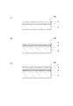
このようなハーフトーン位相シフトマスクブランクとして具体的には、図2(A)に示されるものが挙げられる。図2(A)は、本発明のハーフトーン位相シフトマスクブランクの一例を示す断面図であり、このハーフトーン位相シフトマスクブランク100は、透明基板10と、透明基板10上に形成されたハーフトーン位相シフト膜1と、ハーフトーン位相シフト膜1上に形成された第2の層2とを備える。
Specific examples of such a halftone phase shift mask blank include those shown in FIG. FIG. 2A is a cross-sectional view showing an example of the halftone phase shift mask blank of the present invention. The halftone phase shift mask blank 100 includes a
本発明のハーフトーン位相シフトマスクブランクには、ハーフトーン位相シフト膜の上に、第2の層として、遮光膜を設けることができる。また、第2の層として、遮光膜と反射防止膜とを組み合わせて設けることもできる。遮光膜を含む第2の層を設けることにより、ハーフトーン位相シフトマスクに、露光光を完全に遮光する領域を設けることができる。この遮光膜及び反射防止膜は、エッチングにおける加工補助膜としても利用可能である。遮光膜及び反射防止膜の膜構成及び材料については多数の報告(例えば、特開2007−33469号公報(特許文献4)、特開2007−233179号公報(特許文献5)など)があるが、好ましい遮光膜と反射防止膜との組み合わせの膜構成としては、例えば、クロムを含む材料の遮光膜を設け、更に、遮光膜からの反射を低減させるクロムを含む材料の反射防止膜を設けたものなどが挙げられる。遮光膜及び反射防止膜は、いずれも単層で構成しても、多層で構成してもよい。遮光膜や反射防止膜のクロムを含む材料としては、クロム単体、クロム酸化物(CrO)、クロム窒化物(CrN)、クロム炭化物(CrC)、クロム酸化窒化物(CrON)、クロム酸化炭化物(CrOC)、クロム窒化炭化物(CrNC)、クロム酸化窒化炭化物(CrONC)等のクロム化合物などが挙げられる。 In the halftone phase shift mask blank of the present invention, a light shielding film can be provided as the second layer on the halftone phase shift film. In addition, a light shielding film and an antireflection film can be provided in combination as the second layer. By providing the second layer including the light shielding film, the halftone phase shift mask can be provided with a region that completely shields the exposure light. The light shielding film and the antireflection film can be used as a processing auxiliary film in etching. There are many reports (for example, JP 2007-33469 A (Patent Document 4), JP 2007-233179 A (Patent Document 5), etc.) regarding the film configuration and materials of the light shielding film and the antireflection film. As a preferable film configuration of a combination of a light shielding film and an antireflection film, for example, a light shielding film made of a material containing chromium is provided, and further, an antireflection film made of a material containing chromium that reduces reflection from the light shielding film is provided. Etc. Both the light shielding film and the antireflection film may be composed of a single layer or multiple layers. Examples of the material containing chromium for the light shielding film and the antireflection film include chromium alone, chromium oxide (CrO), chromium nitride (CrN), chromium carbide (CrC), chromium oxynitride (CrON), and chromium oxide carbide (CrOC). ), Chromium nitride carbide (CrNC), chromium oxynitride carbide (CrONC), and the like.
第2の層が遮光膜、又は遮光膜と反射防止膜との組み合わせである場合、遮光膜のクロム化合物中のクロムの含有率は40原子%以上、特に60原子%以上で、100原子%未満、特に99原子%以下、とりわけ90原子%以下であることが好ましい。酸素の含有率は0原子%以上で、60原子%以下、特に40原子%以下であることが好ましく、エッチング速度を調整する必要がある場合は、1原子%以上であることが好ましい。窒素の含有率は0原子%以上で、50原子%以下、特に40原子%以下であることが好ましく、エッチング速度を調整する必要がある場合は、1原子%以上であることが好ましい。炭素の含有率は0原子%以上で、20原子%以下、特に10原子%以下であることが好ましく、エッチング速度を調整する必要がある場合は、1原子%以上であることが好ましい。この場合、クロム、酸素、窒素及び炭素の合計の含有率は95原子%以上、特に99原子%以上、とりわけ100原子%であることが好ましい。 When the second layer is a light shielding film or a combination of a light shielding film and an antireflection film, the chromium content in the chromium compound of the light shielding film is 40 atomic% or more, particularly 60 atomic% or more and less than 100 atomic%. In particular, it is preferably 99 atomic% or less, particularly 90 atomic% or less. The oxygen content is 0 atom% or more, preferably 60 atom% or less, particularly preferably 40 atom% or less. When the etching rate needs to be adjusted, it is preferably 1 atom% or more. The nitrogen content is 0 atomic% or more, preferably 50 atomic% or less, and particularly preferably 40 atomic% or less. When the etching rate needs to be adjusted, it is preferably 1 atomic% or more. The carbon content is 0 atom% or more, preferably 20 atom% or less, particularly preferably 10 atom% or less. When the etching rate needs to be adjusted, it is preferably 1 atom% or more. In this case, the total content of chromium, oxygen, nitrogen and carbon is preferably 95 atomic% or more, particularly 99 atomic% or more, and particularly preferably 100 atomic%.
また、第2の層が遮光膜と反射防止膜との組み合わせである場合、反射防止膜はクロム化合物であることが好ましく、クロム化合物中のクロムの含有率は30原子%以上、特に35原子%以上で、70原子%以下、特に50原子%以下であることが好ましい。酸素の含有率は60原子%以下であることが好ましく、1原子%以上、特に20原子%以上であることがより好ましい。窒素の含有率は50原子%以下、特に30原子%以下であることが好ましく、1原子%以上、特に3原子%以上であることがより好ましい。炭素の含有率は0原子%以上で、20原子%以下、特に5原子%以下であることが好ましく、エッチング速度を調整する必要がある場合は、1原子%以上であることが好ましい。この場合、クロム、酸素、窒素及び炭素の合計の含有率は95原子%以上、特に99原子%以上、とりわけ100原子%であることが好ましい。 Further, when the second layer is a combination of a light shielding film and an antireflection film, the antireflection film is preferably a chromium compound, and the chromium content in the chromium compound is 30 atomic% or more, particularly 35 atomic%. Above, it is preferable that it is 70 atomic% or less, especially 50 atomic% or less. The oxygen content is preferably 60 atomic percent or less, more preferably 1 atomic percent or more, and particularly preferably 20 atomic percent or more. The nitrogen content is preferably 50 atom% or less, particularly preferably 30 atom% or less, more preferably 1 atom% or more, and particularly preferably 3 atom% or more. The carbon content is 0 atom% or more, preferably 20 atom% or less, and particularly preferably 5 atom% or less. When the etching rate needs to be adjusted, it is preferably 1 atom% or more. In this case, the total content of chromium, oxygen, nitrogen and carbon is preferably 95 atomic% or more, particularly 99 atomic% or more, and particularly preferably 100 atomic%.
第2の層が遮光膜、又は遮光膜と反射防止膜との組み合わせである場合、第2の層の膜厚は、通常20〜100nm、好ましくは40〜70nmである。また、波長200nm以下の露光光に対するハーフトーン位相シフト膜と第2の層との合計の光学濃度が2.0以上、特に2.5以上、とりわけ3.0以上となるようにすることが好ましい。 When the second layer is a light shielding film or a combination of a light shielding film and an antireflection film, the film thickness of the second layer is usually 20 to 100 nm, preferably 40 to 70 nm. The total optical density of the halftone phase shift film and the second layer with respect to exposure light having a wavelength of 200 nm or less is preferably 2.0 or more, particularly 2.5 or more, particularly 3.0 or more. .
本発明のハーフトーン位相シフトマスクブランクの第2の層の上には、単層又は多層からなる第3の層を設けることができる。第3の層は、通常、第2の層に隣接して設けられる。この第3の層として具体的には、第2の層のパターン形成においてハードマスクとして機能する加工補助膜、遮光膜、遮光膜と反射防止膜との組み合わせなどが挙げられる。第3の層の材料としては、ケイ素を含む材料が好適であり、特に、クロムを含まないものが好ましい。 A third layer consisting of a single layer or multiple layers can be provided on the second layer of the halftone phase shift mask blank of the present invention. The third layer is usually provided adjacent to the second layer. Specific examples of the third layer include a processing auxiliary film that functions as a hard mask in the pattern formation of the second layer, a light shielding film, and a combination of a light shielding film and an antireflection film. As the material of the third layer, a material containing silicon is preferable, and a material not containing chromium is particularly preferable.
このようなハーフトーン位相シフトマスクブランクとして具体的には、図2(B)に示されるものが挙げられる。図2(B)は、本発明のハーフトーン位相シフトマスクブランクの一例を示す断面図であり、このハーフトーン位相シフトマスクブランク100は、透明基板10と、透明基板10上に形成されたハーフトーン位相シフト膜1と、ハーフトーン位相シフト膜1上に形成された第2の層2と、第2の層2上に形成された第3の層3とを備える。
Specific examples of such a halftone phase shift mask blank include those shown in FIG. FIG. 2B is a cross-sectional view showing an example of the halftone phase shift mask blank of the present invention. The halftone phase shift mask blank 100 includes a
第2の層が遮光膜、又は遮光膜と反射防止膜との組み合わせである場合、第3の層として、第2の層のパターン形成においてハードマスクとして機能する加工補助膜(エッチングマスク膜)を設けることができる。また、後述する第4の層を設ける場合、この第3の層を、第4の層のパターン形成においてエッチングストッパーとして機能する加工補助膜(エッチングストッパー膜)として利用することもできる。この加工補助膜は、第2の層とエッチング特性が異なる材料、例えば、クロムを含む材料のエッチングに適用される塩素系ドライエッチングに耐性を有する材料、具体的には、SF6やCF4などのフッ素系ガスでエッチングできるケイ素を含む材料とすることが好ましい。ケイ素を含む材料として具体的には、ケイ素単体、ケイ素と、窒素及び酸素の一方又は双方とを含む材料、ケイ素と遷移金属とを含む材料、ケイ素と、窒素及び酸素の一方又は双方と、遷移金属とを含む材料等のケイ素化合物などが挙げられ、遷移金属としては、モリブデン、タンタル、ジルコニウムなどが挙げられる。 When the second layer is a light shielding film or a combination of a light shielding film and an antireflection film, a processing auxiliary film (etching mask film) that functions as a hard mask in pattern formation of the second layer is used as the third layer. Can be provided. When a fourth layer described later is provided, the third layer can be used as a processing auxiliary film (etching stopper film) that functions as an etching stopper in pattern formation of the fourth layer. This processing auxiliary film is a material having etching characteristics different from those of the second layer, for example, a material resistant to chlorine-based dry etching applied to etching of a material containing chromium, specifically, SF 6 , CF 4, etc. It is preferable to use a material containing silicon that can be etched with a fluorine-based gas. Specifically, as a material containing silicon, silicon alone, a material containing silicon and one or both of nitrogen and oxygen, a material containing silicon and a transition metal, silicon, one or both of nitrogen and oxygen, transition Examples thereof include silicon compounds such as materials containing metals, and examples of transition metals include molybdenum, tantalum, and zirconium.
第3の層が加工補助膜である場合、加工補助膜はケイ素化合物であることが好ましく、ケイ素化合物中のケイ素の含有率は20原子%以上、特に33原子%以上で、95原子%以下、特に80原子%以下であることが好ましい。窒素の含有率は0原子%以上で、50原子%以下、特に30原子%以下であることが好ましく、エッチング速度を調整する必要がある場合は、1原子%以上であることが好ましい。酸素の含有率は0原子%以上、特に20原子%以上で、70原子%以下、特に66原子%以下であることが好ましく、エッチング速度を調整する必要がある場合は、1原子%以上であることが好ましい。遷移金属の含有率は0原子%以上で、35原子%以下、特に20原子%以下であることが好ましく、遷移金属を含有する場合は、1原子%以上であることが好ましい。この場合、ケイ素、酸素、窒素及び遷移金属の合計の含有率は95原子%以上、特に99原子%以上、とりわけ100原子%であることが好ましい。 When the third layer is a processing auxiliary film, the processing auxiliary film is preferably a silicon compound, and the silicon content in the silicon compound is 20 atomic% or more, particularly 33 atomic% or more, and 95 atomic% or less. In particular, it is preferably 80 atomic% or less. The nitrogen content is 0 atom% or more, preferably 50 atom% or less, particularly preferably 30 atom% or less. When the etching rate needs to be adjusted, it is preferably 1 atom% or more. The oxygen content is 0 atomic% or more, particularly 20 atomic% or more, preferably 70 atomic% or less, particularly 66 atomic% or less, and when the etching rate needs to be adjusted, it is 1 atomic% or more. It is preferable. The content of the transition metal is 0 atomic% or more and preferably 35 atomic% or less, particularly preferably 20 atomic% or less. When the transition metal is contained, it is preferably 1 atomic% or more. In this case, the total content of silicon, oxygen, nitrogen and transition metal is preferably 95 atomic% or more, particularly 99 atomic% or more, and particularly preferably 100 atomic%.
第2の層が遮光膜、又は遮光膜と反射防止膜との組み合わせ、第3の層が加工補助膜である場合、第2の層の膜厚は、通常20〜100nm、好ましくは40〜70nmであり、第3の層の膜厚は、通常1〜30nm、好ましくは2〜15nmである。また、波長200nm以下の露光光に対するハーフトーン位相シフト膜と第2の層との合計の光学濃度が2.0以上、特に2.5以上、とりわけ3.0以上となるようにすることが好ましい。 When the second layer is a light shielding film or a combination of a light shielding film and an antireflection film, and the third layer is a processing aid film, the thickness of the second layer is usually 20 to 100 nm, preferably 40 to 70 nm. The thickness of the third layer is usually 1 to 30 nm, preferably 2 to 15 nm. The total optical density of the halftone phase shift film and the second layer with respect to exposure light having a wavelength of 200 nm or less is preferably 2.0 or more, particularly 2.5 or more, particularly 3.0 or more. .
また、第2の層が加工補助膜である場合、第3の層として、遮光膜を設けることができる。また、第3の層として、遮光膜と反射防止膜とを組み合わせて設けることもできる。この場合、第2の層は、ハーフトーン位相シフト膜のパターン形成においてハードマスクとして機能する加工補助膜(エッチングマスク膜)であり、第3の層のパターン形成においてエッチングストッパーとして機能する加工補助膜(エッチングストッパー膜)として利用することもできる。加工補助膜の例としては、特開2007−241065号公報(特許文献6)で示されているようなクロムを含む材料で構成された膜が挙げられる。加工補助膜は、単層で構成しても、多層で構成してもよい。加工補助膜のクロムを含む材料としては、クロム単体、クロム酸化物(CrO)、クロム窒化物(CrN)、クロム炭化物(CrC)、クロム酸化窒化物(CrON)、クロム酸化炭化物(CrOC)、クロム窒化炭化物(CrNC)、クロム酸化窒化炭化物(CrONC)等のクロム化合物などが挙げられる。 Further, when the second layer is a processing auxiliary film, a light shielding film can be provided as the third layer. In addition, a light shielding film and an antireflection film can be provided in combination as the third layer. In this case, the second layer is a processing auxiliary film (etching mask film) that functions as a hard mask in the pattern formation of the halftone phase shift film, and a processing auxiliary film that functions as an etching stopper in the pattern formation of the third layer. It can also be used as (etching stopper film). An example of the processing auxiliary film is a film made of a material containing chromium as disclosed in Japanese Patent Application Laid-Open No. 2007-244105 (Patent Document 6). The processing auxiliary film may be composed of a single layer or a multilayer. The processing auxiliary film containing chromium includes chromium alone, chromium oxide (CrO), chromium nitride (CrN), chromium carbide (CrC), chromium oxynitride (CrON), chromium oxide carbide (CrOC), chromium Examples thereof include chromium compounds such as nitrided carbide (CrNC) and chromium oxynitride carbide (CrONC).
第2の層が加工補助膜である場合、第2の層中のクロムの含有率は40原子%以上、特に50原子%以上で、100原子%以下、特に99原子%以下、とりわけ90原子%以下であることが好ましい。酸素の含有率は0原子%以上で、60原子%以下、特に55原子%以下であることが好ましく、エッチング速度を調整する必要がある場合は、1原子%以上であることが好ましい。窒素の含有率は0原子%以上で、50原子%以下、特に40原子%以下であることが好ましく、エッチング速度を調整する必要がある場合は、1原子%以上であることが好ましい。炭素の含有率は0原子%以上で、20原子%以下、特に10原子%以下であることが好ましく、エッチング速度を調整する必要がある場合は、1原子%以上であることが好ましい。この場合、クロム、酸素、窒素及び炭素の合計の含有率は95原子%以上、特に99原子%以上、とりわけ100原子%であることが好ましい。 When the second layer is a processing aid film, the chromium content in the second layer is 40 atomic% or more, particularly 50 atomic% or more, 100 atomic% or less, especially 99 atomic% or less, especially 90 atomic%. The following is preferable. The oxygen content is 0 atom% or more, preferably 60 atom% or less, and particularly preferably 55 atom% or less. When the etching rate needs to be adjusted, it is preferably 1 atom% or more. The nitrogen content is 0 atomic% or more, preferably 50 atomic% or less, and particularly preferably 40 atomic% or less. When the etching rate needs to be adjusted, it is preferably 1 atomic% or more. The carbon content is 0 atom% or more, preferably 20 atom% or less, particularly preferably 10 atom% or less. When the etching rate needs to be adjusted, it is preferably 1 atom% or more. In this case, the total content of chromium, oxygen, nitrogen and carbon is preferably 95 atomic% or more, particularly 99 atomic% or more, and particularly preferably 100 atomic%.
一方、第3の層の遮光膜及び反射防止膜は、第2の層とエッチング特性が異なる材料、例えば、クロムを含む材料のエッチングに適用される塩素系ドライエッチングに耐性を有する材料、具体的には、SF6やCF4などのフッ素系ガスでエッチングできるケイ素を含む材料とすることが好ましい。ケイ素を含む材料として具体的には、ケイ素単体、ケイ素と、窒素及び酸素の一方又は双方とを含む材料、ケイ素と遷移金属とを含む材料、ケイ素と、窒素及び酸素の一方又は双方と、遷移金属とを含む材料等のケイ素化合物などが挙げられ、遷移金属としては、モリブデン、タンタル、ジルコニウムなどが挙げられる。 On the other hand, the light-shielding film and the antireflection film of the third layer are materials having etching characteristics different from those of the second layer, for example, a material having resistance to chlorine-based dry etching applied to etching of a material containing chromium. It is preferable to use a silicon-containing material that can be etched with a fluorine-based gas such as SF 6 or CF 4 . Specifically, as a material containing silicon, silicon alone, a material containing silicon and one or both of nitrogen and oxygen, a material containing silicon and a transition metal, silicon, one or both of nitrogen and oxygen, transition Examples thereof include silicon compounds such as materials containing metals, and examples of transition metals include molybdenum, tantalum, and zirconium.
第3の層が遮光膜、又は遮光膜と反射防止膜との組み合わせである場合、遮光膜及び反射防止膜はケイ素化合物であることが好ましく、ケイ素化合物中のケイ素の含有率は10原子%以上、特に30原子%以上で、100原子%未満、特に95原子%以下であることが好ましい。窒素の含有率は0原子%以上で、50原子%以下、特に40原子%以下、とりわけ20原子%以下であることが好ましく、エッチング速度を調整する必要がある場合は、1原子%以上であることが好ましい。酸素の含有率は0原子%以上で、60原子%以下、特に30原子%以下であることが好ましく、エッチング速度を調整する必要がある場合は、1原子%以上であることが好ましい。遷移金属の含有率は0原子%以上で、35原子%以下、特に20原子%以下であることが好ましく、遷移金属を含有する場合は、1原子%以上であることが好ましい。この場合、ケイ素、酸素、窒素及び遷移金属の合計の含有率は95原子%以上、特に99原子%以上、とりわけ100原子%であることが好ましい。 When the third layer is a light shielding film or a combination of a light shielding film and an antireflection film, the light shielding film and the antireflection film are preferably silicon compounds, and the silicon content in the silicon compound is 10 atomic% or more. In particular, it is preferably 30 atomic% or more and less than 100 atomic%, particularly 95 atomic% or less. The nitrogen content is 0 atomic% or more, preferably 50 atomic% or less, particularly preferably 40 atomic% or less, and particularly preferably 20 atomic% or less. When the etching rate needs to be adjusted, it is 1 atomic% or more. It is preferable. The oxygen content is 0 atom% or more, preferably 60 atom% or less, particularly preferably 30 atom% or less. When the etching rate needs to be adjusted, it is preferably 1 atom% or more. The content of the transition metal is 0 atomic% or more and preferably 35 atomic% or less, particularly preferably 20 atomic% or less. When the transition metal is contained, it is preferably 1 atomic% or more. In this case, the total content of silicon, oxygen, nitrogen and transition metal is preferably 95 atomic% or more, particularly 99 atomic% or more, and particularly preferably 100 atomic%.
第2の層が加工補助膜、第3の層が遮光膜、又は遮光膜と反射防止膜との組み合わせである場合、第2の層の膜厚は、通常1〜20nm、好ましくは2〜10nmであり、第3の層の膜厚は、通常20〜100nm、好ましくは30〜70nmである。また、波長200nm以下の露光光に対するハーフトーン位相シフト膜と第2の層と第3の層との合計の光学濃度が2.0以上、特に2.5以上、とりわけ3.0以上となるようにすることが好ましい。 When the second layer is a processing aid film and the third layer is a light shielding film, or a combination of a light shielding film and an antireflection film, the thickness of the second layer is usually 1 to 20 nm, preferably 2 to 10 nm. The film thickness of the third layer is usually 20 to 100 nm, preferably 30 to 70 nm. Further, the total optical density of the halftone phase shift film, the second layer, and the third layer with respect to exposure light having a wavelength of 200 nm or less is 2.0 or more, particularly 2.5 or more, particularly 3.0 or more. It is preferable to make it.
本発明のハーフトーン位相シフトマスクブランクの第3の層の上には、単層又は多層からなる第4の層を設けることができる。第4の層は、通常、第3の層に隣接して設けられる。この第4の層として具体的には、第3の層のパターン形成においてハードマスクとして機能する加工補助膜などが挙げられる。第4の層の材料としては、クロムを含む材料が好適である。 A fourth layer consisting of a single layer or multiple layers can be provided on the third layer of the halftone phase shift mask blank of the present invention. The fourth layer is usually provided adjacent to the third layer. Specific examples of the fourth layer include a processing aid film that functions as a hard mask in pattern formation of the third layer. As the material for the fourth layer, a material containing chromium is suitable.
このようなハーフトーン位相シフトマスクブランクとして具体的には、図2(C)に示されるものが挙げられる。図2(C)は、本発明のハーフトーン位相シフトマスクブランクの一例を示す断面図であり、このハーフトーン位相シフトマスクブランク100は、透明基板10と、透明基板10上に形成されたハーフトーン位相シフト膜1と、ハーフトーン位相シフト膜1上に形成された第2の層2と、第2の層2上に形成された第3の層3と、第3の層3上に形成された第4の層4とを備える。
A specific example of such a halftone phase shift mask blank is shown in FIG. FIG. 2C is a cross-sectional view showing an example of the halftone phase shift mask blank of the present invention. The halftone phase shift mask blank 100 includes a
第3の層が遮光膜、又は遮光膜と反射防止膜との組み合わせである場合、第4の層として、第3の層のパターン形成においてハードマスクとして機能する加工補助膜(エッチングマスク膜)を設けることができる。この加工補助膜は、第3の層とエッチング特性が異なる材料、例えば、ケイ素を含む材料のエッチングに適用されるフッ素系ドライエッチングに耐性を有する材料、具体的には、酸素を含有する塩素系ガスでエッチングできるクロムを含む材料とすることが好ましい。クロムを含む材料として具体的には、クロム単体、クロム酸化物(CrO)、クロム窒化物(CrN)、クロム炭化物(CrC)、クロム酸化窒化物(CrON)、クロム酸化炭化物(CrOC)、クロム窒化炭化物(CrNC)、クロム酸化窒化炭化物(CrONC)等のクロム化合物などが挙げられる。 When the third layer is a light shielding film or a combination of a light shielding film and an antireflection film, a processing auxiliary film (etching mask film) that functions as a hard mask in pattern formation of the third layer is used as the fourth layer. Can be provided. This processing aid film is a material having etching characteristics different from those of the third layer, for example, a material resistant to fluorine-based dry etching applied to etching of a material containing silicon, specifically, a chlorine-based material containing oxygen. A material containing chromium that can be etched with a gas is preferable. Specific examples of the material containing chromium include chromium alone, chromium oxide (CrO), chromium nitride (CrN), chromium carbide (CrC), chromium oxynitride (CrON), chromium oxide carbide (CrOC), and chromium nitride. Examples thereof include chromium compounds such as carbide (CrNC) and chromium oxynitride carbide (CrONC).
第4の層が加工補助膜である場合、第4の層中のクロムの含有率は40原子%以上、特に50原子%以上で、100原子%以下、特に99原子%以下、とりわけ90原子%以下であることが好ましい。酸素の含有率は0原子%以上で、60原子%以下、特に40原子%以下であることが好ましく、エッチング速度を調整する必要がある場合は、1原子%以上であることが好ましい。窒素の含有率は0原子%以上で、50原子%以下、特に40原子%以下であることが好ましく、エッチング速度を調整する必要がある場合は、1原子%以上であることが好ましい。炭素の含有率は0原子%以上で、20原子%以下、特に10原子%以下であることが好ましく、エッチング速度を調整する必要がある場合は、1原子%以上であることが好ましい。この場合、クロム、酸素、窒素及び炭素の合計の含有率は95原子%以上、特に99原子%以上、とりわけ100原子%であることが好ましい。 When the fourth layer is a processing aid film, the chromium content in the fourth layer is 40 atomic% or more, particularly 50 atomic% or more, and 100 atomic% or less, particularly 99 atomic% or less, especially 90 atomic%. The following is preferable. The oxygen content is 0 atom% or more, preferably 60 atom% or less, particularly preferably 40 atom% or less. When the etching rate needs to be adjusted, it is preferably 1 atom% or more. The nitrogen content is 0 atomic% or more, preferably 50 atomic% or less, and particularly preferably 40 atomic% or less. When the etching rate needs to be adjusted, it is preferably 1 atomic% or more. The carbon content is 0 atom% or more, preferably 20 atom% or less, particularly preferably 10 atom% or less. When the etching rate needs to be adjusted, it is preferably 1 atom% or more. In this case, the total content of chromium, oxygen, nitrogen and carbon is preferably 95 atomic% or more, particularly 99 atomic% or more, and particularly preferably 100 atomic%.
第2の層が加工補助膜、第3の層が遮光膜、又は遮光膜と反射防止膜との組み合わせ、第4の層が加工補助膜である場合、第2の層の膜厚は、通常1〜20nm、好ましくは2〜10nmであり、第3の層の膜厚は、通常20〜100nm、好ましくは30〜70nmであり、第4の層の膜厚は、通常1〜30nm、好ましくは2〜20nmである。また、波長200nm以下の露光光に対するハーフトーン位相シフト膜と第2の層と第3の層との合計の光学濃度が2.0以上、特に2.5以上、とりわけ3.0以上となるようにすることが好ましい。 When the second layer is a processing auxiliary film, the third layer is a light shielding film, or a combination of a light shielding film and an antireflection film, and the fourth layer is a processing auxiliary film, the thickness of the second layer is usually 1 to 20 nm, preferably 2 to 10 nm, the thickness of the third layer is usually 20 to 100 nm, preferably 30 to 70 nm, and the thickness of the fourth layer is usually 1 to 30 nm, preferably 2-20 nm. Further, the total optical density of the halftone phase shift film, the second layer, and the third layer with respect to exposure light having a wavelength of 200 nm or less is 2.0 or more, particularly 2.5 or more, particularly 3.0 or more. It is preferable to make it.
第2の層及び第4の層のクロムを含む材料で構成された膜は、クロムターゲット、クロムに酸素、窒素及び炭素から選ばれるいずれか1種又は2種以上を添加したターゲットなどを用い、Ar、He、Neなどの希ガスに、成膜する膜の組成に応じて、酸素含有ガス、窒素含有ガス、炭素含有ガスなどから選ばれる反応性ガスを適宜添加したスパッタガスを用いた反応性スパッタにより成膜することができる。 The film made of the material containing chromium of the second layer and the fourth layer uses a chromium target, a target obtained by adding one or more selected from oxygen, nitrogen, and carbon to chromium, and the like. Reactivity using a sputtering gas in which a reactive gas selected from an oxygen-containing gas, a nitrogen-containing gas, a carbon-containing gas, or the like is appropriately added to a rare gas such as Ar, He, or Ne according to the composition of a film to be formed. A film can be formed by sputtering.
一方、第3の層のケイ素を含む材料で構成された膜は、ケイ素ターゲット、窒化ケイ素ターゲット、ケイ素と窒化ケイ素の双方を含むターゲット、遷移金属ターゲット、ケイ素と遷移金属との複合ターゲットなどを用い、Ar、He、Neなどの希ガスに、成膜する膜の組成に応じて、酸素含有ガス、窒素含有ガス、炭素含有ガスなどから選ばれる反応性ガスを適宜添加したスパッタガスを用いた反応性スパッタにより成膜することができる。 On the other hand, the film made of the silicon-containing material of the third layer uses a silicon target, a silicon nitride target, a target containing both silicon and silicon nitride, a transition metal target, a composite target of silicon and transition metal, and the like. Reaction using a sputtering gas in which a reactive gas selected from an oxygen-containing gas, a nitrogen-containing gas, a carbon-containing gas, or the like is appropriately added to a rare gas such as Ar, He, or Ne according to the composition of a film to be formed The film can be formed by reactive sputtering.
本発明のハーフトーン位相シフトマスクは、ハーフトーン位相シフトマスクブランクから、常法により製造することができる。例えば、ハーフトーン位相シフト膜の上に、第2の層として、クロムを含む材料の膜が形成されているハーフトーン位相シフトマスクブランクでは、例えば、下記の工程でハーフトーン位相シフトマスクを製造することができる。 The halftone phase shift mask of the present invention can be manufactured from a halftone phase shift mask blank by a conventional method. For example, in a halftone phase shift mask blank in which a film of a material containing chromium is formed as the second layer on the halftone phase shift film, for example, a halftone phase shift mask is manufactured by the following process. be able to.
まず、ハーフトーン位相シフトマスクブランクの第2の層上に、電子線レジスト膜を成膜し、電子線によるパターン描画を行った後、所定の現像操作によってレジストパターンを得る。次に、得られたレジストパターンをエッチングマスクとして、酸素を含有する塩素系ドライエッチングにより、第2の層にレジストパターンを転写して、第2の層のパターンを得る。次に、得られた第2の層のパターンをエッチングマスクとして、フッ素系ドライエッチングにより、ハーフトーン位相シフト膜に第2の層のパターンを転写して、ハーフトーン位相シフト膜パターンを得る。ここで、第2の層の一部を残す必要がある場合は、その部分を保護するレジストパターンを、第2の層の上に形成した後、酸素を含有する塩素系ドライエッチングにより、レジストパターンで保護されていない部分の第2の層を除去する。そして、レジストパターンを常法により除去して、ハーフトーン位相シフトマスクを得ることができる。 First, an electron beam resist film is formed on the second layer of the halftone phase shift mask blank, a pattern is drawn with an electron beam, and then a resist pattern is obtained by a predetermined development operation. Next, using the obtained resist pattern as an etching mask, the resist pattern is transferred to the second layer by chlorine-based dry etching containing oxygen to obtain a pattern of the second layer. Next, by using the obtained second layer pattern as an etching mask, the second layer pattern is transferred to the halftone phase shift film by fluorine-based dry etching to obtain a halftone phase shift film pattern. Here, when it is necessary to leave a part of the second layer, a resist pattern for protecting the part is formed on the second layer, and then the resist pattern is formed by chlorine-based dry etching containing oxygen. The portion of the second layer not protected by is removed. Then, the halftone phase shift mask can be obtained by removing the resist pattern by a conventional method.
また、ハーフトーン位相シフト膜の上に、第2の層として、クロムを含む材料の遮光膜、又は遮光膜と反射防止膜との組み合わせが形成され、第2の層の上に、第3の層として、ケイ素を含む材料の加工補助膜が形成されているハーフトーン位相シフトマスクブランクでは、例えば、下記の工程でハーフトーン位相シフトマスクを製造することができる。 Further, on the halftone phase shift film, a light shielding film of a material containing chromium or a combination of a light shielding film and an antireflection film is formed as a second layer, and a third layer is formed on the second layer. In a halftone phase shift mask blank in which a processing auxiliary film of a material containing silicon is formed as a layer, for example, a halftone phase shift mask can be manufactured by the following steps.
まず、ハーフトーン位相シフトマスクブランクの第3の層の上に、電子線レジスト膜を成膜し、電子線によるパターン描画を行った後、所定の現像操作によってレジストパターンを得る。次に、得られたレジストパターンをエッチングマスクとして、フッ素系ドライエッチングにより、第3の層にレジストパターンを転写して、第3の層のパターンを得る。次に、得られた第3の層のパターンをエッチングマスクとして、酸素を含有する塩素系ドライエッチングにより、第2の層に第3の層のパターンを転写して、第2の層のパターンを得る。次に、レジストパターンを除去した後、得られた第2の層のパターンをエッチングマスクとして、フッ素系ドライエッチングにより、ハーフトーン位相シフト膜に第2の層のパターンを転写して、ハーフトーン位相シフト膜パターンを得ると同時に、第3の層のパターンを除去する。次に、第2の層を残す部分を保護するレジストパターンを、第2の層の上に形成した後、酸素を含有する塩素系ドライエッチングにより、レジストパターンで保護されていない部分の第2の層を除去する。そして、レジストパターンを常法により除去して、ハーフトーン位相シフトマスクを得ることができる。 First, an electron beam resist film is formed on the third layer of the halftone phase shift mask blank, a pattern is drawn with an electron beam, and then a resist pattern is obtained by a predetermined development operation. Next, using the obtained resist pattern as an etching mask, the resist pattern is transferred to the third layer by fluorine-based dry etching to obtain a pattern of the third layer. Next, using the pattern of the obtained third layer as an etching mask, the pattern of the third layer is transferred to the second layer by chlorine-based dry etching containing oxygen, and the pattern of the second layer is formed. obtain. Next, after removing the resist pattern, the pattern of the second layer is transferred to the halftone phase shift film by fluorine-based dry etching using the pattern of the obtained second layer as an etching mask. At the same time as obtaining the shift film pattern, the pattern of the third layer is removed. Next, after forming a resist pattern for protecting the portion where the second layer remains on the second layer, the second portion of the portion not protected by the resist pattern is subjected to chlorine-based dry etching containing oxygen. Remove the layer. Then, the halftone phase shift mask can be obtained by removing the resist pattern by a conventional method.
一方、ハーフトーン位相シフト膜の上に、第2の層として、クロムを含む材料の加工補助膜が形成され、第2の層の上に、第3の層として、ケイ素を含む材料の遮光膜、又は遮光膜と反射防止膜との組み合わせが形成されているハーフトーン位相シフトマスクブランクでは、例えば、下記の工程でハーフトーン位相シフトマスクを製造することができる。 On the other hand, a processing auxiliary film made of a material containing chromium is formed as a second layer on the halftone phase shift film, and a light shielding film made of a material containing silicon is used as the third layer on the second layer. In a halftone phase shift mask blank in which a combination of a light shielding film and an antireflection film is formed, for example, a halftone phase shift mask can be manufactured by the following process.
まず、ハーフトーン位相シフトマスクブランクの第3の層の上に、電子線レジスト膜を成膜し、電子線によるパターン描画を行った後、所定の現像操作によってレジストパターンを得る。次に、得られたレジストパターンをエッチングマスクとして、フッ素系ドライエッチングにより、第3の層にレジストパターンを転写して、第3の層のパターンを得る。次に、得られた第3の層のパターンをエッチングマスクとして、酸素を含有する塩素系ドライエッチングにより、第2の層に第3の層のパターンを転写して、ハーフトーン位相シフト膜を除去する部分の第2の層が除去された第2の層のパターンを得る。次に、レジストパターンを除去し、第3の層を残す部分を保護するレジストパターンを、第3の層の上に形成した後、得られた第2の層のパターンをエッチングマスクとして、フッ素系ドライエッチングにより、ハーフトーン位相シフト膜に第2の層のパターンを転写して、ハーフトーン位相シフト膜パターンを得ると同時に、レジストパターンで保護されていない部分の第3の層を除去する。次に、レジストパターンを常法により除去する。そして、酸素を含有する塩素系ドライエッチングにより、第3の層が除去された部分の第2の層を除去して、ハーフトーン位相シフトマスクを得ることができる。 First, an electron beam resist film is formed on the third layer of the halftone phase shift mask blank, a pattern is drawn with an electron beam, and then a resist pattern is obtained by a predetermined development operation. Next, using the obtained resist pattern as an etching mask, the resist pattern is transferred to the third layer by fluorine-based dry etching to obtain a pattern of the third layer. Next, using the obtained pattern of the third layer as an etching mask, the pattern of the third layer is transferred to the second layer by chlorine-based dry etching containing oxygen, and the halftone phase shift film is removed. A pattern of the second layer from which the second layer of the portion to be removed is removed is obtained. Next, after removing the resist pattern and forming a resist pattern on the third layer to protect the portion where the third layer remains, the obtained second layer pattern is used as an etching mask to form a fluorine-based material. The pattern of the second layer is transferred to the halftone phase shift film by dry etching to obtain a halftone phase shift film pattern, and at the same time, the portion of the third layer not protected by the resist pattern is removed. Next, the resist pattern is removed by a conventional method. Then, the second layer where the third layer has been removed is removed by chlorine-based dry etching containing oxygen, whereby a halftone phase shift mask can be obtained.
更に、ハーフトーン位相シフト膜の上に、第2の層として、クロムを含む材料の加工補助膜が形成され、第2の層の上に、第3の層として、ケイ素を含む材料の遮光膜、又は遮光膜と反射防止膜との組み合わせが形成され、更に、第3の層の上に、第4の層として、クロムを含む材料の加工補助膜が形成されているハーフトーン位相シフトマスクブランクでは、例えば、下記の工程でハーフトーン位相シフトマスクを製造することができる。 Further, a processing aid film made of a material containing chromium is formed as a second layer on the halftone phase shift film, and a light shielding film made of a material containing silicon is used as the third layer on the second layer. Or a halftone phase shift mask blank in which a combination of a light shielding film and an antireflection film is formed, and a processing auxiliary film of a material containing chromium is formed as a fourth layer on the third layer. Then, for example, a halftone phase shift mask can be manufactured by the following steps.
まず、ハーフトーン位相シフトマスクブランクの第4の層の上に、電子線レジスト膜を成膜し、電子線によるパターン描画を行った後、所定の現像操作によってレジストパターンを得る。次に、得られたレジストパターンをエッチングマスクとして、酸素を含有する塩素系ドライエッチングにより、第4の層にレジストパターンを転写して、第4の層のパターンを得る。次に、得られた第4の層のパターンをエッチングマスクとして、フッ素系ドライエッチングにより、第3の層に第4の層のパターンを転写して、第3の層のパターンを得る。次に、レジストパターンを除去し、第3の層を残す部分を保護するレジストパターンを、第4の層の上に形成した後、得られた第3の層のパターンをエッチングマスクとして、酸素を含有する塩素系ドライエッチングにより、第2の層に第3の層のパターンを転写して第2の層のパターンを得ると同時に、レジストパターンで保護されていない部分の第4の層を除去する。次に、第2の層のパターンをエッチングマスクとして、フッ素系ドライエッチングにより、ハーフトーン位相シフト膜に第2の層のパターンを転写して、ハーフトーン位相シフト膜パターンを得ると同時に、レジストパターンで保護されていない部分の第3の層を除去する。次に、レジストパターンを常法により除去する。そして、酸素を含有する塩素系ドライエッチングにより、第3の層が除去された部分の第2の層と、レジストパターンが除去された部分の第4の層を除去して、ハーフトーン位相シフトマスクを得ることができる。 First, an electron beam resist film is formed on the fourth layer of the halftone phase shift mask blank, a pattern is drawn with an electron beam, and then a resist pattern is obtained by a predetermined development operation. Next, using the obtained resist pattern as an etching mask, the resist pattern is transferred to the fourth layer by chlorine-based dry etching containing oxygen to obtain a pattern of the fourth layer. Next, using the pattern of the obtained fourth layer as an etching mask, the pattern of the fourth layer is transferred to the third layer by fluorine-based dry etching to obtain the pattern of the third layer. Next, after removing the resist pattern and forming a resist pattern on the fourth layer to protect the portion where the third layer is to be left, oxygen is applied using the obtained third layer pattern as an etching mask. The chlorine layer dry etching contained therein transfers the pattern of the third layer to the second layer to obtain the pattern of the second layer, and at the same time, the portion of the fourth layer not protected by the resist pattern is removed. . Next, using the second layer pattern as an etching mask, the second layer pattern is transferred to the halftone phase shift film by fluorine-based dry etching to obtain a halftone phase shift film pattern. The third layer that is not protected by is removed. Next, the resist pattern is removed by a conventional method. Then, the second layer from which the third layer has been removed and the fourth layer from which the resist pattern has been removed are removed by chlorine-based dry etching containing oxygen, and a halftone phase shift mask. Can be obtained.
本発明のハーフトーン位相マスクは、被加工基板にハーフピッチ50nm以下、特に30nm以下、とりわけ20nm以下のパターンを形成するためのフォトリソグラフィにおいて、被加工基板上に形成したフォトレジスト膜に、ArFエキシマレーザー光(波長193nm)、F2レーザー光(波長157nm)などの波長200nm以下の露光光でパターンを転写する露光において特に有効である。 The halftone phase mask of the present invention is an ArF excimer formed on a photoresist film formed on a substrate to be processed in photolithography for forming a pattern having a half pitch of 50 nm or less, particularly 30 nm or less, particularly 20 nm or less on a substrate to be processed. This is particularly effective in exposure in which a pattern is transferred with exposure light having a wavelength of 200 nm or less, such as laser light (wavelength 193 nm) and F 2 laser light (wavelength 157 nm).
本発明のパターン露光方法では、ハーフトーン位相シフトマスクブランクから製造されたハーフトーン位相シフトマスクを用い、ハーフトーン位相シフト膜のパターンを含むフォトマスクパターンに、露光光を照射して、被加工基板上に形成したフォトマスクパターンの露光対象であるフォトレジスト膜に、フォトマスクパターンを転写する。露光光の照射は、ドライ条件による露光でも、液浸露光でもよいが、本発明のパターン露光方法は、実生産において比較的短時間に累積照射エネルギー量が上がってしまう、液浸露光により、特に、300mm以上のウェハーを被加工基板として液浸露光により、フォトマスクパターンを露光する際に、特に有効である。 In the pattern exposure method of the present invention, a halftone phase shift mask manufactured from a halftone phase shift mask blank is used, exposure light is irradiated to a photomask pattern including a pattern of a halftone phase shift film, and a substrate to be processed The photomask pattern is transferred to the photoresist film that is the exposure target of the photomask pattern formed above. Irradiation of exposure light may be exposure under dry conditions or immersion exposure, but the pattern exposure method of the present invention is particularly effective due to immersion exposure in which the cumulative irradiation energy amount increases in a relatively short time in actual production. This is particularly effective when a photomask pattern is exposed by immersion exposure using a wafer of 300 mm or more as a substrate to be processed.
以下、実施例及び比較例を示して、本発明を具体的に説明するが、本発明は、下記の実施例に制限されるものではない。 EXAMPLES Hereinafter, although an Example and a comparative example are shown and this invention is demonstrated concretely, this invention is not restrict | limited to the following Example.
[実施例1]
152mm角、厚さ6.35mmの石英基板上に、スパッタターゲットとしてケイ素ターゲットを用い、スパッタガスとして、窒素ガスとアルゴンガスとを用いて、SiNのハーフトーン位相シフト膜を成膜した。この膜の波長193nmの光(ArFエキシマレーザー、以下同じ)での位相差が178°となるように成膜時間を調節して成膜したところ、波長193nmの光での透過率が6%で、膜厚が61nmであった。また、この膜の組成をXPS(X線光電子分光分析法、以下同じ)で測定したところ、原子比でSi:N=48:52であった。また、この膜の波長193nmの光での屈折率nは2.6、消衰係数kは0.64であった。更に、この膜を、室温(23℃)で、120分間、アンモニア過水洗浄液(28質量%アンモニア水:30質量%過酸化水素水:水=1:1:100(体積比))に浸漬することにより薬品耐性を評価したところ、位相差の変化は0.10°未満であった。
[Example 1]
A SiN halftone phase shift film was formed on a 152 mm square and 6.35 mm thick quartz substrate using a silicon target as a sputtering target and nitrogen gas and argon gas as sputtering gases. When the film was formed by adjusting the film formation time so that the phase difference of light with a wavelength of 193 nm (ArF excimer laser, the same applies hereinafter) was 178 °, the transmittance with light with a wavelength of 193 nm was 6%. The film thickness was 61 nm. Further, the composition of this film was measured by XPS (X-ray photoelectron spectroscopy, the same shall apply hereinafter). Further, the refractive index n of this film with light having a wavelength of 193 nm was 2.6, and the extinction coefficient k was 0.64. Further, this membrane is immersed in an ammonia perwater washing solution (28% by mass ammonia water: 30% by mass hydrogen peroxide solution: water = 1: 1: 100 (volume ratio)) at room temperature (23 ° C.) for 120 minutes. As a result, when the chemical resistance was evaluated, the change in phase difference was less than 0.10 °.
[実施例2]
152mm角、厚さ6.35mmの石英基板上に、スパッタターゲットとしてケイ素ターゲットを用い、スパッタガスとして、窒素ガスとアルゴンガスとを用いて、SiNのハーフトーン位相シフト膜を成膜した。この膜の波長193nmの光での位相差が180°となるように成膜時間を調節して成膜したところ、波長193nmの光での透過率が12%で、膜厚が60nmであった。また、この膜の組成をXPSで測定したところ、原子比でSi:N=47:53であった。また、この膜の波長193nmの光での屈折率nは2.6、消衰係数kは0.46であった。更に、この膜の耐薬品性を実施例1と同様にして評価したところ、位相差の変化は0.40°であった。
[Example 2]
A SiN halftone phase shift film was formed on a 152 mm square and 6.35 mm thick quartz substrate using a silicon target as a sputtering target and nitrogen gas and argon gas as sputtering gases. When this film was formed by adjusting the film formation time so that the phase difference with light with a wavelength of 193 nm was 180 °, the transmittance with light with a wavelength of 193 nm was 12% and the film thickness was 60 nm. . Further, when the composition of this film was measured by XPS, the atomic ratio was Si: N = 47: 53. The refractive index n of this film at a wavelength of 193 nm was 2.6, and the extinction coefficient k was 0.46. Furthermore, when the chemical resistance of this film was evaluated in the same manner as in Example 1, the change in phase difference was 0.40 °.
[実施例3]
152mm角、厚さ6.35mmの石英基板上に、スパッタターゲットとしてケイ素ターゲットを用い、スパッタガスとして、酸素ガスと窒素ガスとアルゴンガスとを用いて、SiONのハーフトーン位相シフト膜を成膜した。この膜の波長193nmの光での位相差が177°となるように成膜時間を調節して成膜したところ、波長193nmの光での透過率が7%で、膜厚が62nmであった。また、この膜の組成をXPSで測定したところ、原子比でSi:N:O=46:50:4であった。また、この膜の波長193nmの光での屈折率nは2.6、消衰係数kは0.59であった。更に、この膜の耐薬品性を実施例1と同様にして評価したところ、位相差の変化は0.24°であった。
[Example 3]
A SiON halftone phase shift film was formed on a 152 mm square and 6.35 mm thick quartz substrate using a silicon target as a sputtering target and oxygen gas, nitrogen gas and argon gas as sputtering gases. . When the film was formed by adjusting the film formation time so that the phase difference with light with a wavelength of 193 nm was 177 °, the transmittance with light with a wavelength of 193 nm was 7% and the film thickness was 62 nm. . Further, when the composition of this film was measured by XPS, the atomic ratio was Si: N: O = 46: 50: 4. In addition, the refractive index n of this film at a wavelength of 193 nm was 2.6, and the extinction coefficient k was 0.59. Furthermore, when the chemical resistance of this film was evaluated in the same manner as in Example 1, the change in phase difference was 0.24 °.
[実施例4]
152mm角、厚さ6.35mmの石英基板上に、スパッタターゲットとしてケイ素ターゲットを用い、スパッタガスとして、酸素ガスと窒素ガスとアルゴンガスとを用いて、SiONのハーフトーン位相シフト膜を成膜した。この膜の波長193nmの光での位相差が177°となるように成膜時間を調節して成膜したところ、波長193nmの光での透過率が6%で、膜厚が67nmであった。また、この膜の組成をXPSで測定したところ、原子比でSi:N:O=46:45:9であった。また、この膜の波長193nmの光での屈折率nは2.6、消衰係数kは0.59であった。更に、この膜の耐薬品性を実施例1と同様にして評価したところ、位相差の変化は0.13°であった。
[Example 4]
A SiON halftone phase shift film was formed on a 152 mm square and 6.35 mm thick quartz substrate using a silicon target as a sputtering target and oxygen gas, nitrogen gas and argon gas as sputtering gases. . When the film was formed by adjusting the film formation time so that the phase difference with light with a wavelength of 193 nm was 177 °, the transmittance with light with a wavelength of 193 nm was 6% and the film thickness was 67 nm. . Further, when the composition of this film was measured by XPS, the atomic ratio was Si: N: O = 46: 45: 9. In addition, the refractive index n of this film at a wavelength of 193 nm was 2.6, and the extinction coefficient k was 0.59. Furthermore, when the chemical resistance of this film was evaluated in the same manner as in Example 1, the change in phase difference was 0.13 °.
[比較例1]
152mm角、厚さ6.35mmの石英基板上に、スパッタターゲットとして、モリブデンとケイ素をモル比でモリブデン:ケイ素=1:2の比率で含有するターゲットと、ケイ素ターゲットとを用い、スパッタガスとして、酸素ガスと窒素ガスとアルゴンガスとを用いて、MoSiONのハーフトーン位相シフト膜を成膜した。この膜の波長193nmの光での位相差が177°となるように成膜時間を調節して成膜したところ、波長193nmの光での透過率が6%で、膜厚が75nmであった。また、この膜の組成をXPSで測定したところ、原子比でMo:Si:N:O=9:36:45:10であった。また、この膜の波長193nmの光での屈折率nは2.3、消衰係数kは0.54であった。更に、この膜の耐薬品性を実施例1と同様にして評価したところ、位相差の変化は3.91°であった。
[Comparative Example 1]
On a quartz substrate having a size of 152 mm square and a thickness of 6.35 mm, as a sputtering target, a target containing molybdenum and silicon in a molar ratio of molybdenum: silicon = 1: 2 and a silicon target, and as a sputtering gas, A MoSiON halftone phase shift film was formed using oxygen gas, nitrogen gas, and argon gas. When the film was formed by adjusting the film formation time so that the phase difference with light with a wavelength of 193 nm was 177 °, the transmittance with light with a wavelength of 193 nm was 6% and the film thickness was 75 nm. . Moreover, when the composition of this film was measured by XPS, the atomic ratio was Mo: Si: N: O = 9: 36: 45: 10. Further, the refractive index n of this film at a wavelength of 193 nm was 2.3, and the extinction coefficient k was 0.54. Furthermore, when the chemical resistance of this film was evaluated in the same manner as in Example 1, the change in phase difference was 3.91 °.
1 ハーフトーン位相シフト膜
2 第2の層
3 第3の層
4 第4の層
10 透明基板
11 ハーフトーン位相シフト膜パターン
100 ハーフトーン位相シフトマスクブランク
101 ハーフトーン位相シフトマスク
DESCRIPTION OF
Claims (7)
上記ハーフトーン位相シフト膜が、
ケイ素及び窒素からなるケイ素系材料、又はケイ素、窒素及び酸素からなり、該酸素の含有率が6原子%以下のケイ素系材料で構成され、屈折率nが2.4以上、消衰係数kが0.4以上0.7以下の単層で形成され、
膜厚が67nm以下であることを特徴とするハーフトーン位相シフトマスクブランク。 A halftone phase shift mask blank having a halftone phase shift film on a transparent substrate having a wavelength of 200 nm or less, a phase shift amount of 150 to 200 °, and a transmittance of 3% or more and 12% or less,
The halftone phase shift film is
A silicon-based material composed of silicon and nitrogen, or a silicon-based material composed of silicon, nitrogen and oxygen and having an oxygen content of 6 atomic% or less, a refractive index n of 2.4 or more, and an extinction coefficient k. Formed with a single layer of 0.4 or more and 0.7 or less,
A halftone phase shift mask blank having a film thickness of 67 nm or less.
上記ハーフトーン位相シフト膜が、
ケイ素及び窒素からなるケイ素系材料、又はケイ素、窒素及び酸素からなり、該酸素の含有率が6原子%以下のケイ素系材料で構成され、屈折率nが2.4以上、消衰係数kが0.4以上0.7以下の単層、又は
ケイ素及び窒素からなるケイ素系材料、又はケイ素、窒素及び酸素からなり、該酸素の含有率が6原子%以下のケイ素系材料で構成され、屈折率nが2.4以上、消衰係数kが0.4以上0.7以下の層を1層以上含む多層で形成され、
膜厚が67nm以下であり、
被加工基板にハーフピッチ50nm以下のパターンを形成するためのフォトリソグラフィにおいて、被加工基板上に形成したフォトレジスト膜に、波長200nm以下の露光光で上記パターンを転写するパターン露光に用いるハーフトーン位相シフトマスク用であることを特徴とするハーフトーン位相シフトマスクブランク。 A halftone phase shift mask blank having a halftone phase shift film on a transparent substrate having a wavelength of 200 nm or less, a phase shift amount of 150 to 200 °, and a transmittance of 3% or more and 12% or less,
The halftone phase shift film is
A silicon-based material composed of silicon and nitrogen, or a silicon-based material composed of silicon, nitrogen and oxygen and having an oxygen content of 6 atomic% or less, a refractive index n of 2.4 or more, and an extinction coefficient k. 0.4 to 0.7 single layer, or
A silicon-based material composed of silicon and nitrogen, or a silicon-based material composed of silicon, nitrogen and oxygen and having an oxygen content of 6 atomic% or less, a refractive index n of 2.4 or more, and an extinction coefficient k. Formed of multiple layers including one or more layers of 0.4 or more and 0.7 or less,
The film thickness is 67 nm or less,
In photolithography for forming a pattern with a half pitch of 50 nm or less on a substrate to be processed, a halftone phase used for pattern exposure in which the pattern is transferred to a photoresist film formed on the substrate to be processed with exposure light having a wavelength of 200 nm or less. features and to Ruha Futon phase shift mask blank that is for shifting mask.
上記ハーフトーン位相シフト膜が、
ケイ素及び窒素からなるケイ素系材料、又はケイ素、窒素及び酸素からなり、該酸素の含有率が6原子%以下のケイ素系材料で構成され、屈折率nが2.4以上、消衰係数kが0.4以上0.7以下の単層で形成され、
膜厚が67nm以下であることを特徴とするハーフトーン位相シフトマスク。 A halftone phase shift mask having a pattern of a halftone phase shift film having a phase shift amount of 150 to 200 ° and a transmittance of 3% or more and 12% or less with light having a wavelength of 200 nm or less on a transparent substrate. ,
The halftone phase shift film is
A silicon-based material composed of silicon and nitrogen, or a silicon-based material composed of silicon, nitrogen and oxygen and having an oxygen content of 6 atomic% or less, a refractive index n of 2.4 or more, and an extinction coefficient k. Formed with a single layer of 0.4 or more and 0.7 or less,
A halftone phase shift mask having a film thickness of 67 nm or less.
上記ハーフトーン位相シフト膜が、
ケイ素及び窒素からなるケイ素系材料、又はケイ素、窒素及び酸素からなり、該酸素の含有率が6原子%以下のケイ素系材料で構成され、屈折率nが2.4以上、消衰係数kが0.4以上0.7以下の単層、又は
ケイ素及び窒素からなるケイ素系材料、又はケイ素、窒素及び酸素からなり、該酸素の含有率が6原子%以下のケイ素系材料で構成され、屈折率nが2.4以上、消衰係数kが0.4以上0.7以下の層を1層以上含む多層で形成され、
膜厚が67nm以下であり、
被加工基板にハーフピッチ50nm以下のパターンを形成するためのフォトリソグラフィにおいて、被加工基板上に形成したフォトレジスト膜に、波長200nm以下の露光光で上記パターンを転写するパターン露光用であることを特徴とするハーフトーン位相シフトマスク。 A halftone phase shift mask having a pattern of a halftone phase shift film having a phase shift amount of 150 to 200 ° and a transmittance of 3% or more and 12% or less with light having a wavelength of 200 nm or less on a transparent substrate. ,
The halftone phase shift film is
A silicon-based material composed of silicon and nitrogen, or a silicon-based material composed of silicon, nitrogen and oxygen and having an oxygen content of 6 atomic% or less, a refractive index n of 2.4 or more, and an extinction coefficient k. 0.4 to 0.7 single layer, or
A silicon-based material composed of silicon and nitrogen, or a silicon-based material composed of silicon, nitrogen and oxygen and having an oxygen content of 6 atomic% or less, a refractive index n of 2.4 or more, and an extinction coefficient k. Formed of multiple layers including one or more layers of 0.4 or more and 0.7 or less,
The film thickness is 67 nm or less,
In photolithography for forming a pattern with a half pitch of 50 nm or less on a substrate to be processed, it is for pattern exposure that transfers the pattern to the photoresist film formed on the substrate to be processed with exposure light having a wavelength of 200 nm or less. features and be Ruha Futon phase shift mask.
透明基板上に、波長200nm以下の光で、位相シフト量が150〜200°、かつ透過率が3%以上12%以下であるハーフトーン位相シフト膜のパターンを有し、
上記ハーフトーン位相シフト膜が、
ケイ素及び窒素からなるケイ素系材料、又はケイ素、窒素及び酸素からなり、該酸素の含有率が6原子%以下のケイ素系材料で構成され、屈折率nが2.4以上、消衰係数kが0.4以上0.7以下の単層、又は
ケイ素及び窒素からなるケイ素系材料、又はケイ素、窒素及び酸素からなり、該酸素の含有率が6原子%以下のケイ素系材料で構成され、屈折率nが2.4以上、消衰係数kが0.4以上0.7以下の層を1層以上含む多層で形成され、
膜厚が67nm以下であるハーフトーン位相シフトマスクを用いることを特徴とするパターン露光方法。 In photolithography for forming a pattern with a half pitch of 50 nm or less on a substrate to be processed, a pattern exposure method for transferring the pattern to a photoresist film formed on the substrate to be processed with exposure light having a wavelength of 200 nm or less,
On a transparent substrate, it has a pattern of a halftone phase shift film having a phase shift amount of 150 to 200 ° and a transmittance of 3% or more and 12% or less with light having a wavelength of 200 nm or less,
The halftone phase shift film is
A silicon-based material composed of silicon and nitrogen, or a silicon-based material composed of silicon, nitrogen and oxygen and having an oxygen content of 6 atomic% or less, a refractive index n of 2.4 or more, and an extinction coefficient k. A single layer of 0.4 or more and 0.7 or less, or a silicon-based material composed of silicon and nitrogen, or a silicon-based material composed of silicon, nitrogen and oxygen, the oxygen content of which is 6 atomic% or less, and is refracted. Formed of a multilayer including one or more layers having a rate n of 2.4 or more and an extinction coefficient k of 0.4 or more and 0.7 or less,
A pattern exposure method using a halftone phase shift mask having a film thickness of 67 nm or less.
Priority Applications (7)
| Application Number | Priority Date | Filing Date | Title |
|---|---|---|---|
| JP2015073045A JP6380204B2 (en) | 2015-03-31 | 2015-03-31 | Halftone phase shift mask blank, halftone phase shift mask and pattern exposure method |
| EP16161074.6A EP3086180B1 (en) | 2015-03-31 | 2016-03-18 | Halftone phase shift mask blank, halftone phase shift mask, and pattern exposure method |
| US15/078,618 US9927695B2 (en) | 2015-03-31 | 2016-03-23 | Halftone phase shift mask blank, halftone phase shift mask, and pattern exposure method |
| KR1020160036801A KR101899202B1 (en) | 2015-03-31 | 2016-03-28 | Halftone phase shift mask blank, halftone phase shift mask, and pattern exposure method |
| SG10201602448YA SG10201602448YA (en) | 2015-03-31 | 2016-03-29 | Halftone Phase Shift Mask Blank, Halftone Phase Shift Mask, And Pattern Exposure Method |
| TW105110126A TWI663467B (en) | 2015-03-31 | 2016-03-30 | Halftone phase shift mask blank, halftone phase shift mask, and pattern exposure method |
| CN201610195910.9A CN106019809B (en) | 2015-03-31 | 2016-03-31 | Halftone phase shift mask blank, halftone phase shift mask, and pattern exposure method |
Applications Claiming Priority (1)
| Application Number | Priority Date | Filing Date | Title |
|---|---|---|---|
| JP2015073045A JP6380204B2 (en) | 2015-03-31 | 2015-03-31 | Halftone phase shift mask blank, halftone phase shift mask and pattern exposure method |
Publications (2)
| Publication Number | Publication Date |
|---|---|
| JP2016191882A JP2016191882A (en) | 2016-11-10 |
| JP6380204B2 true JP6380204B2 (en) | 2018-08-29 |
Family
ID=55587143
Family Applications (1)
| Application Number | Title | Priority Date | Filing Date |
|---|---|---|---|
| JP2015073045A Active JP6380204B2 (en) | 2015-03-31 | 2015-03-31 | Halftone phase shift mask blank, halftone phase shift mask and pattern exposure method |
Country Status (7)
| Country | Link |
|---|---|
| US (1) | US9927695B2 (en) |
| EP (1) | EP3086180B1 (en) |
| JP (1) | JP6380204B2 (en) |
| KR (1) | KR101899202B1 (en) |
| CN (1) | CN106019809B (en) |
| SG (1) | SG10201602448YA (en) |
| TW (1) | TWI663467B (en) |
Families Citing this family (12)
| Publication number | Priority date | Publication date | Assignee | Title |
|---|---|---|---|---|
| US10678125B2 (en) * | 2016-03-02 | 2020-06-09 | Shin-Etsu Chemical Co., Ltd. | Photomask blank and method for preparing photomask |
| JP6743679B2 (en) * | 2016-03-02 | 2020-08-19 | 信越化学工業株式会社 | Photomask blank and photomask manufacturing method |
| WO2018181891A1 (en) * | 2017-03-31 | 2018-10-04 | 凸版印刷株式会社 | Phase shift mask blank, phase shift mask and manufacturing method for phase shift mask |
| JP6432636B2 (en) | 2017-04-03 | 2018-12-05 | 凸版印刷株式会社 | Photomask blank, photomask and photomask manufacturing method |
| JP6791031B2 (en) * | 2017-06-13 | 2020-11-25 | 信越化学工業株式会社 | Photomask blank and its manufacturing method |
| JP6753375B2 (en) * | 2017-07-28 | 2020-09-09 | 信越化学工業株式会社 | Photomask blank, photomask blank manufacturing method and photomask manufacturing method |
| JP6998181B2 (en) * | 2017-11-14 | 2022-02-04 | アルバック成膜株式会社 | Mask blank, phase shift mask and its manufacturing method |
| WO2019102990A1 (en) * | 2017-11-24 | 2019-05-31 | Hoya株式会社 | Mask blank, phase shift mask, and method for manufacturing semiconductor device |
| SG11202007542WA (en) * | 2018-02-27 | 2020-09-29 | Hoya Corp | Mask blank, phase shift mask, and method of manufacturing semiconductor device |
| JP6896694B2 (en) * | 2018-12-25 | 2021-06-30 | Hoya株式会社 | Mask blank, phase shift mask, phase shift mask manufacturing method and semiconductor device manufacturing method |
| JP7264083B2 (en) * | 2019-03-29 | 2023-04-25 | 信越化学工業株式会社 | PHASE SHIFT MASK BLANKS, MANUFACTURING METHOD THEREOF AND PHASE SHIFT MASK |
| CN115343910A (en) * | 2021-05-12 | 2022-11-15 | 上海传芯半导体有限公司 | Phase-shifting mask and manufacturing method thereof |
Family Cites Families (20)
| Publication number | Priority date | Publication date | Assignee | Title |
|---|---|---|---|---|
| JP3064769B2 (en) | 1992-11-21 | 2000-07-12 | アルバック成膜株式会社 | PHASE SHIFT MASK, ITS MANUFACTURING METHOD, AND EXPOSURE METHOD USING THE PHASE SHIFT MASK |
| JP3286103B2 (en) * | 1995-02-15 | 2002-05-27 | 株式会社東芝 | Method and apparatus for manufacturing exposure mask |
| KR0166497B1 (en) * | 1995-03-24 | 1999-01-15 | 김주용 | Phase inversion mask and the method of production therefrom |
| US5939227A (en) * | 1998-03-09 | 1999-08-17 | Rochester Institute Of Technology | Multi-layered attenuated phase shift mask and a method for making the mask |
| JP2002169265A (en) * | 2000-12-01 | 2002-06-14 | Hoya Corp | Photomask blank and method of manufacturing photomask blank |
| JP3988041B2 (en) | 2002-10-08 | 2007-10-10 | 信越化学工業株式会社 | Halftone phase shift mask blank and manufacturing method thereof |
| TWI348590B (en) * | 2004-03-31 | 2011-09-11 | Shinetsu Chemical Co | Halftone phase shift mask blank, halftone phase shift mask, and pattern transfer method |
| EP2657768B1 (en) * | 2004-06-16 | 2020-08-05 | Hoya Corporation | Photomask blank and photomask |
| JP5165833B2 (en) * | 2005-02-04 | 2013-03-21 | 信越化学工業株式会社 | Photomask blank, photomask, and photomask blank manufacturing method |
| DE602006021102D1 (en) | 2005-07-21 | 2011-05-19 | Shinetsu Chemical Co | Photomask blank, photomask and their manufacturing process |
| JP4933753B2 (en) | 2005-07-21 | 2012-05-16 | 信越化学工業株式会社 | Phase shift mask blank, phase shift mask, and manufacturing method thereof |
| JP4551344B2 (en) | 2006-03-02 | 2010-09-29 | 信越化学工業株式会社 | Photomask blank and photomask |
| JP4509050B2 (en) | 2006-03-10 | 2010-07-21 | 信越化学工業株式会社 | Photomask blank and photomask |
| JP4714180B2 (en) | 2007-05-01 | 2011-06-29 | 株式会社東芝 | Photomask management method, photomask cleaning possible number generation method, and photomask management system |
| TWI457697B (en) * | 2009-01-15 | 2014-10-21 | Shinetsu Chemical Co | Photomask making method, photomask blank and dry etching method |
| JP5644293B2 (en) * | 2010-09-10 | 2014-12-24 | 信越化学工業株式会社 | Method of designing transition metal silicon-based material film |
| KR102390253B1 (en) * | 2013-01-15 | 2022-04-22 | 호야 가부시키가이샤 | Mask blank, phase-shift mask, and method for manufacturing semiconductor device |
| JP6373607B2 (en) * | 2013-03-08 | 2018-08-15 | Hoya株式会社 | Manufacturing method of mask blank and manufacturing method of phase shift mask |
| KR102251087B1 (en) * | 2013-08-21 | 2021-05-14 | 다이니폰 인사츠 가부시키가이샤 | Mask blank, mask blank with negative resist film, phase shift mask, and method for producing patterned body using same |
| JP6524614B2 (en) * | 2014-05-27 | 2019-06-05 | 大日本印刷株式会社 | Mask blanks, mask blanks with negative resist film, phase shift mask, and method of manufacturing patterned body using the same |
-
2015
- 2015-03-31 JP JP2015073045A patent/JP6380204B2/en active Active
-
2016
- 2016-03-18 EP EP16161074.6A patent/EP3086180B1/en active Active
- 2016-03-23 US US15/078,618 patent/US9927695B2/en active Active
- 2016-03-28 KR KR1020160036801A patent/KR101899202B1/en active IP Right Grant
- 2016-03-29 SG SG10201602448YA patent/SG10201602448YA/en unknown
- 2016-03-30 TW TW105110126A patent/TWI663467B/en active
- 2016-03-31 CN CN201610195910.9A patent/CN106019809B/en active Active
Also Published As
| Publication number | Publication date |
|---|---|
| KR20160117250A (en) | 2016-10-10 |
| CN106019809B (en) | 2020-11-10 |
| US20160291456A1 (en) | 2016-10-06 |
| US9927695B2 (en) | 2018-03-27 |
| TWI663467B (en) | 2019-06-21 |
| KR101899202B1 (en) | 2018-09-14 |
| TW201704848A (en) | 2017-02-01 |
| EP3086180A1 (en) | 2016-10-26 |
| SG10201602448YA (en) | 2016-10-28 |
| JP2016191882A (en) | 2016-11-10 |
| CN106019809A (en) | 2016-10-12 |
| EP3086180B1 (en) | 2020-04-29 |
Similar Documents
| Publication | Publication Date | Title |
|---|---|---|
| JP6418035B2 (en) | Phase shift mask blanks and phase shift masks | |
| JP6341129B2 (en) | Halftone phase shift mask blank and halftone phase shift mask | |
| KR102228886B1 (en) | Halftone phase shift mask blank and halftone phase shift mask | |
| JP6380204B2 (en) | Halftone phase shift mask blank, halftone phase shift mask and pattern exposure method | |
| JP6264238B2 (en) | Halftone phase shift photomask blank, halftone phase shift photomask, and pattern exposure method | |
| KR102145240B1 (en) | Halftone phase shift photomask blank and making method | |
| JP6500791B2 (en) | Halftone phase shift photomask blank and method of manufacturing the same | |
| JP6287932B2 (en) | Method for manufacturing halftone phase shift photomask blank | |
| JP6477159B2 (en) | Halftone phase shift mask blank and method of manufacturing halftone phase shift mask blank | |
| JP6677139B2 (en) | Manufacturing method of halftone phase shift type photomask blank | |
| JP6579219B2 (en) | Halftone phase shift mask blank and halftone phase shift mask | |
| JP2018063441A (en) | Half tone phase shift type photomask blank, half tone phase shift type photomask and pattern exposure method | |
| JP6627926B2 (en) | Method for manufacturing phase shift mask blanks | |
| JP6551585B2 (en) | Halftone phase shift photomask blank and method of manufacturing the same | |
| JP2020021087A (en) | Halftone phase shift type photomask blank and halftone phase shift type photomask |
Legal Events
| Date | Code | Title | Description |
|---|---|---|---|
| A621 | Written request for application examination |
Free format text: JAPANESE INTERMEDIATE CODE: A621 Effective date: 20170222 |
|
| A977 | Report on retrieval |
Free format text: JAPANESE INTERMEDIATE CODE: A971007 Effective date: 20171130 |
|
| A131 | Notification of reasons for refusal |
Free format text: JAPANESE INTERMEDIATE CODE: A131 Effective date: 20171205 |
|
| A521 | Written amendment |
Free format text: JAPANESE INTERMEDIATE CODE: A523 Effective date: 20180115 |
|
| TRDD | Decision of grant or rejection written | ||
| A01 | Written decision to grant a patent or to grant a registration (utility model) |
Free format text: JAPANESE INTERMEDIATE CODE: A01 Effective date: 20180703 |
|
| A61 | First payment of annual fees (during grant procedure) |
Free format text: JAPANESE INTERMEDIATE CODE: A61 Effective date: 20180716 |
|
| R150 | Certificate of patent or registration of utility model |
Ref document number: 6380204 Country of ref document: JP Free format text: JAPANESE INTERMEDIATE CODE: R150 |