JP6374492B2 - Trench Gate Trench Field Plate Semi-Vertical Semi-lateral MOSFET - Google Patents
Trench Gate Trench Field Plate Semi-Vertical Semi-lateral MOSFET Download PDFInfo
- Publication number
- JP6374492B2 JP6374492B2 JP2016520007A JP2016520007A JP6374492B2 JP 6374492 B2 JP6374492 B2 JP 6374492B2 JP 2016520007 A JP2016520007 A JP 2016520007A JP 2016520007 A JP2016520007 A JP 2016520007A JP 6374492 B2 JP6374492 B2 JP 6374492B2
- Authority
- JP
- Japan
- Prior art keywords
- trench
- gate
- closed
- sidewall
- mos transistor
- Prior art date
- Legal status (The legal status is an assumption and is not a legal conclusion. Google has not performed a legal analysis and makes no representation as to the accuracy of the status listed.)
- Active
Links
- 239000000758 substrate Substances 0.000 claims description 67
- 239000004065 semiconductor Substances 0.000 claims description 54
- 210000000746 body region Anatomy 0.000 claims description 17
- 229910052581 Si3N4 Inorganic materials 0.000 claims description 2
- XUIMIQQOPSSXEZ-UHFFFAOYSA-N Silicon Chemical compound [Si] XUIMIQQOPSSXEZ-UHFFFAOYSA-N 0.000 claims description 2
- 229910052710 silicon Inorganic materials 0.000 claims description 2
- 239000010703 silicon Substances 0.000 claims description 2
- HQVNEWCFYHHQES-UHFFFAOYSA-N silicon nitride Chemical compound N12[Si]34N5[Si]62N3[Si]51N64 HQVNEWCFYHHQES-UHFFFAOYSA-N 0.000 claims description 2
- 238000000034 method Methods 0.000 description 14
- 238000004519 manufacturing process Methods 0.000 description 7
- 239000002019 doping agent Substances 0.000 description 6
- 238000005468 ion implantation Methods 0.000 description 6
- 238000002955 isolation Methods 0.000 description 5
- VYPSYNLAJGMNEJ-UHFFFAOYSA-N Silicium dioxide Chemical compound O=[Si]=O VYPSYNLAJGMNEJ-UHFFFAOYSA-N 0.000 description 4
- 239000000463 material Substances 0.000 description 4
- 238000001020 plasma etching Methods 0.000 description 4
- 229910021420 polycrystalline silicon Inorganic materials 0.000 description 4
- 230000015572 biosynthetic process Effects 0.000 description 3
- 230000015556 catabolic process Effects 0.000 description 3
- 239000003989 dielectric material Substances 0.000 description 3
- 230000005684 electric field Effects 0.000 description 3
- 229920005591 polysilicon Polymers 0.000 description 3
- OAICVXFJPJFONN-UHFFFAOYSA-N Phosphorus Chemical compound [P] OAICVXFJPJFONN-UHFFFAOYSA-N 0.000 description 2
- 238000005229 chemical vapour deposition Methods 0.000 description 2
- 229910052698 phosphorus Inorganic materials 0.000 description 2
- 239000011574 phosphorus Substances 0.000 description 2
- 235000012239 silicon dioxide Nutrition 0.000 description 2
- 239000000377 silicon dioxide Substances 0.000 description 2
- 238000000137 annealing Methods 0.000 description 1
- 239000004020 conductor Substances 0.000 description 1
- 239000007943 implant Substances 0.000 description 1
- 229910044991 metal oxide Inorganic materials 0.000 description 1
- 150000004706 metal oxides Chemical class 0.000 description 1
- 229910021421 monocrystalline silicon Inorganic materials 0.000 description 1
- 238000000059 patterning Methods 0.000 description 1
- 238000000206 photolithography Methods 0.000 description 1
- 238000005498 polishing Methods 0.000 description 1
- 239000000126 substance Substances 0.000 description 1
Images


Classifications
-
- H—ELECTRICITY
- H01—ELECTRIC ELEMENTS
- H01L—SEMICONDUCTOR DEVICES NOT COVERED BY CLASS H10
- H01L29/00—Semiconductor devices adapted for rectifying, amplifying, oscillating or switching, or capacitors or resistors with at least one potential-jump barrier or surface barrier, e.g. PN junction depletion layer or carrier concentration layer; Details of semiconductor bodies or of electrodes thereof ; Multistep manufacturing processes therefor
- H01L29/66—Types of semiconductor device ; Multistep manufacturing processes therefor
- H01L29/66007—Multistep manufacturing processes
- H01L29/66075—Multistep manufacturing processes of devices having semiconductor bodies comprising group 14 or group 13/15 materials
- H01L29/66227—Multistep manufacturing processes of devices having semiconductor bodies comprising group 14 or group 13/15 materials the devices being controllable only by the electric current supplied or the electric potential applied, to an electrode which does not carry the current to be rectified, amplified or switched, e.g. three-terminal devices
- H01L29/66409—Unipolar field-effect transistors
- H01L29/66477—Unipolar field-effect transistors with an insulated gate, i.e. MISFET
- H01L29/66674—DMOS transistors, i.e. MISFETs with a channel accommodating body or base region adjoining a drain drift region
- H01L29/66712—Vertical DMOS transistors, i.e. VDMOS transistors
-
- H—ELECTRICITY
- H01—ELECTRIC ELEMENTS
- H01L—SEMICONDUCTOR DEVICES NOT COVERED BY CLASS H10
- H01L21/00—Processes or apparatus adapted for the manufacture or treatment of semiconductor or solid state devices or of parts thereof
- H01L21/02—Manufacture or treatment of semiconductor devices or of parts thereof
- H01L21/04—Manufacture or treatment of semiconductor devices or of parts thereof the devices having at least one potential-jump barrier or surface barrier, e.g. PN junction, depletion layer or carrier concentration layer
- H01L21/18—Manufacture or treatment of semiconductor devices or of parts thereof the devices having at least one potential-jump barrier or surface barrier, e.g. PN junction, depletion layer or carrier concentration layer the devices having semiconductor bodies comprising elements of Group IV of the Periodic System or AIIIBV compounds with or without impurities, e.g. doping materials
- H01L21/22—Diffusion of impurity materials, e.g. doping materials, electrode materials, into or out of a semiconductor body, or between semiconductor regions; Interactions between two or more impurities; Redistribution of impurities
- H01L21/225—Diffusion of impurity materials, e.g. doping materials, electrode materials, into or out of a semiconductor body, or between semiconductor regions; Interactions between two or more impurities; Redistribution of impurities using diffusion into or out of a solid from or into a solid phase, e.g. a doped oxide layer
-
- H—ELECTRICITY
- H01—ELECTRIC ELEMENTS
- H01L—SEMICONDUCTOR DEVICES NOT COVERED BY CLASS H10
- H01L21/00—Processes or apparatus adapted for the manufacture or treatment of semiconductor or solid state devices or of parts thereof
- H01L21/02—Manufacture or treatment of semiconductor devices or of parts thereof
- H01L21/04—Manufacture or treatment of semiconductor devices or of parts thereof the devices having at least one potential-jump barrier or surface barrier, e.g. PN junction, depletion layer or carrier concentration layer
- H01L21/18—Manufacture or treatment of semiconductor devices or of parts thereof the devices having at least one potential-jump barrier or surface barrier, e.g. PN junction, depletion layer or carrier concentration layer the devices having semiconductor bodies comprising elements of Group IV of the Periodic System or AIIIBV compounds with or without impurities, e.g. doping materials
- H01L21/26—Bombardment with radiation
- H01L21/263—Bombardment with radiation with high-energy radiation
- H01L21/265—Bombardment with radiation with high-energy radiation producing ion implantation
- H01L21/26506—Bombardment with radiation with high-energy radiation producing ion implantation in group IV semiconductors
- H01L21/26513—Bombardment with radiation with high-energy radiation producing ion implantation in group IV semiconductors of electrically active species
-
- H—ELECTRICITY
- H01—ELECTRIC ELEMENTS
- H01L—SEMICONDUCTOR DEVICES NOT COVERED BY CLASS H10
- H01L21/00—Processes or apparatus adapted for the manufacture or treatment of semiconductor or solid state devices or of parts thereof
- H01L21/02—Manufacture or treatment of semiconductor devices or of parts thereof
- H01L21/04—Manufacture or treatment of semiconductor devices or of parts thereof the devices having at least one potential-jump barrier or surface barrier, e.g. PN junction, depletion layer or carrier concentration layer
- H01L21/18—Manufacture or treatment of semiconductor devices or of parts thereof the devices having at least one potential-jump barrier or surface barrier, e.g. PN junction, depletion layer or carrier concentration layer the devices having semiconductor bodies comprising elements of Group IV of the Periodic System or AIIIBV compounds with or without impurities, e.g. doping materials
- H01L21/30—Treatment of semiconductor bodies using processes or apparatus not provided for in groups H01L21/20 - H01L21/26
- H01L21/324—Thermal treatment for modifying the properties of semiconductor bodies, e.g. annealing, sintering
-
- H—ELECTRICITY
- H01—ELECTRIC ELEMENTS
- H01L—SEMICONDUCTOR DEVICES NOT COVERED BY CLASS H10
- H01L29/00—Semiconductor devices adapted for rectifying, amplifying, oscillating or switching, or capacitors or resistors with at least one potential-jump barrier or surface barrier, e.g. PN junction depletion layer or carrier concentration layer; Details of semiconductor bodies or of electrodes thereof ; Multistep manufacturing processes therefor
- H01L29/02—Semiconductor bodies ; Multistep manufacturing processes therefor
- H01L29/06—Semiconductor bodies ; Multistep manufacturing processes therefor characterised by their shape; characterised by the shapes, relative sizes, or dispositions of the semiconductor regions ; characterised by the concentration or distribution of impurities within semiconductor regions
- H01L29/0684—Semiconductor bodies ; Multistep manufacturing processes therefor characterised by their shape; characterised by the shapes, relative sizes, or dispositions of the semiconductor regions ; characterised by the concentration or distribution of impurities within semiconductor regions characterised by the shape, relative sizes or dispositions of the semiconductor regions or junctions between the regions
- H01L29/0692—Surface layout
- H01L29/0696—Surface layout of cellular field-effect devices, e.g. multicellular DMOS transistors or IGBTs
-
- H—ELECTRICITY
- H01—ELECTRIC ELEMENTS
- H01L—SEMICONDUCTOR DEVICES NOT COVERED BY CLASS H10
- H01L29/00—Semiconductor devices adapted for rectifying, amplifying, oscillating or switching, or capacitors or resistors with at least one potential-jump barrier or surface barrier, e.g. PN junction depletion layer or carrier concentration layer; Details of semiconductor bodies or of electrodes thereof ; Multistep manufacturing processes therefor
- H01L29/02—Semiconductor bodies ; Multistep manufacturing processes therefor
- H01L29/06—Semiconductor bodies ; Multistep manufacturing processes therefor characterised by their shape; characterised by the shapes, relative sizes, or dispositions of the semiconductor regions ; characterised by the concentration or distribution of impurities within semiconductor regions
- H01L29/08—Semiconductor bodies ; Multistep manufacturing processes therefor characterised by their shape; characterised by the shapes, relative sizes, or dispositions of the semiconductor regions ; characterised by the concentration or distribution of impurities within semiconductor regions with semiconductor regions connected to an electrode carrying current to be rectified, amplified or switched and such electrode being part of a semiconductor device which comprises three or more electrodes
- H01L29/0843—Source or drain regions of field-effect devices
- H01L29/0847—Source or drain regions of field-effect devices of field-effect transistors with insulated gate
- H01L29/0852—Source or drain regions of field-effect devices of field-effect transistors with insulated gate of DMOS transistors
- H01L29/0873—Drain regions
- H01L29/0878—Impurity concentration or distribution
-
- H—ELECTRICITY
- H01—ELECTRIC ELEMENTS
- H01L—SEMICONDUCTOR DEVICES NOT COVERED BY CLASS H10
- H01L29/00—Semiconductor devices adapted for rectifying, amplifying, oscillating or switching, or capacitors or resistors with at least one potential-jump barrier or surface barrier, e.g. PN junction depletion layer or carrier concentration layer; Details of semiconductor bodies or of electrodes thereof ; Multistep manufacturing processes therefor
- H01L29/02—Semiconductor bodies ; Multistep manufacturing processes therefor
- H01L29/06—Semiconductor bodies ; Multistep manufacturing processes therefor characterised by their shape; characterised by the shapes, relative sizes, or dispositions of the semiconductor regions ; characterised by the concentration or distribution of impurities within semiconductor regions
- H01L29/08—Semiconductor bodies ; Multistep manufacturing processes therefor characterised by their shape; characterised by the shapes, relative sizes, or dispositions of the semiconductor regions ; characterised by the concentration or distribution of impurities within semiconductor regions with semiconductor regions connected to an electrode carrying current to be rectified, amplified or switched and such electrode being part of a semiconductor device which comprises three or more electrodes
- H01L29/0843—Source or drain regions of field-effect devices
- H01L29/0847—Source or drain regions of field-effect devices of field-effect transistors with insulated gate
- H01L29/0852—Source or drain regions of field-effect devices of field-effect transistors with insulated gate of DMOS transistors
- H01L29/0873—Drain regions
- H01L29/0882—Disposition
-
- H—ELECTRICITY
- H01—ELECTRIC ELEMENTS
- H01L—SEMICONDUCTOR DEVICES NOT COVERED BY CLASS H10
- H01L29/00—Semiconductor devices adapted for rectifying, amplifying, oscillating or switching, or capacitors or resistors with at least one potential-jump barrier or surface barrier, e.g. PN junction depletion layer or carrier concentration layer; Details of semiconductor bodies or of electrodes thereof ; Multistep manufacturing processes therefor
- H01L29/02—Semiconductor bodies ; Multistep manufacturing processes therefor
- H01L29/06—Semiconductor bodies ; Multistep manufacturing processes therefor characterised by their shape; characterised by the shapes, relative sizes, or dispositions of the semiconductor regions ; characterised by the concentration or distribution of impurities within semiconductor regions
- H01L29/10—Semiconductor bodies ; Multistep manufacturing processes therefor characterised by their shape; characterised by the shapes, relative sizes, or dispositions of the semiconductor regions ; characterised by the concentration or distribution of impurities within semiconductor regions with semiconductor regions connected to an electrode not carrying current to be rectified, amplified or switched and such electrode being part of a semiconductor device which comprises three or more electrodes
- H01L29/1095—Body region, i.e. base region, of DMOS transistors or IGBTs
-
- H—ELECTRICITY
- H01—ELECTRIC ELEMENTS
- H01L—SEMICONDUCTOR DEVICES NOT COVERED BY CLASS H10
- H01L29/00—Semiconductor devices adapted for rectifying, amplifying, oscillating or switching, or capacitors or resistors with at least one potential-jump barrier or surface barrier, e.g. PN junction depletion layer or carrier concentration layer; Details of semiconductor bodies or of electrodes thereof ; Multistep manufacturing processes therefor
- H01L29/40—Electrodes ; Multistep manufacturing processes therefor
- H01L29/402—Field plates
- H01L29/407—Recessed field plates, e.g. trench field plates, buried field plates
-
- H—ELECTRICITY
- H01—ELECTRIC ELEMENTS
- H01L—SEMICONDUCTOR DEVICES NOT COVERED BY CLASS H10
- H01L29/00—Semiconductor devices adapted for rectifying, amplifying, oscillating or switching, or capacitors or resistors with at least one potential-jump barrier or surface barrier, e.g. PN junction depletion layer or carrier concentration layer; Details of semiconductor bodies or of electrodes thereof ; Multistep manufacturing processes therefor
- H01L29/40—Electrodes ; Multistep manufacturing processes therefor
- H01L29/41—Electrodes ; Multistep manufacturing processes therefor characterised by their shape, relative sizes or dispositions
- H01L29/417—Electrodes ; Multistep manufacturing processes therefor characterised by their shape, relative sizes or dispositions carrying the current to be rectified, amplified or switched
- H01L29/41725—Source or drain electrodes for field effect devices
- H01L29/41741—Source or drain electrodes for field effect devices for vertical or pseudo-vertical devices
-
- H—ELECTRICITY
- H01—ELECTRIC ELEMENTS
- H01L—SEMICONDUCTOR DEVICES NOT COVERED BY CLASS H10
- H01L29/00—Semiconductor devices adapted for rectifying, amplifying, oscillating or switching, or capacitors or resistors with at least one potential-jump barrier or surface barrier, e.g. PN junction depletion layer or carrier concentration layer; Details of semiconductor bodies or of electrodes thereof ; Multistep manufacturing processes therefor
- H01L29/40—Electrodes ; Multistep manufacturing processes therefor
- H01L29/41—Electrodes ; Multistep manufacturing processes therefor characterised by their shape, relative sizes or dispositions
- H01L29/423—Electrodes ; Multistep manufacturing processes therefor characterised by their shape, relative sizes or dispositions not carrying the current to be rectified, amplified or switched
- H01L29/42312—Gate electrodes for field effect devices
- H01L29/42316—Gate electrodes for field effect devices for field-effect transistors
- H01L29/4232—Gate electrodes for field effect devices for field-effect transistors with insulated gate
- H01L29/42364—Gate electrodes for field effect devices for field-effect transistors with insulated gate characterised by the insulating layer, e.g. thickness or uniformity
- H01L29/42368—Gate electrodes for field effect devices for field-effect transistors with insulated gate characterised by the insulating layer, e.g. thickness or uniformity the thickness being non-uniform
-
- H—ELECTRICITY
- H01—ELECTRIC ELEMENTS
- H01L—SEMICONDUCTOR DEVICES NOT COVERED BY CLASS H10
- H01L29/00—Semiconductor devices adapted for rectifying, amplifying, oscillating or switching, or capacitors or resistors with at least one potential-jump barrier or surface barrier, e.g. PN junction depletion layer or carrier concentration layer; Details of semiconductor bodies or of electrodes thereof ; Multistep manufacturing processes therefor
- H01L29/66—Types of semiconductor device ; Multistep manufacturing processes therefor
- H01L29/66007—Multistep manufacturing processes
- H01L29/66075—Multistep manufacturing processes of devices having semiconductor bodies comprising group 14 or group 13/15 materials
- H01L29/66227—Multistep manufacturing processes of devices having semiconductor bodies comprising group 14 or group 13/15 materials the devices being controllable only by the electric current supplied or the electric potential applied, to an electrode which does not carry the current to be rectified, amplified or switched, e.g. three-terminal devices
- H01L29/66409—Unipolar field-effect transistors
- H01L29/66477—Unipolar field-effect transistors with an insulated gate, i.e. MISFET
- H01L29/66674—DMOS transistors, i.e. MISFETs with a channel accommodating body or base region adjoining a drain drift region
- H01L29/66712—Vertical DMOS transistors, i.e. VDMOS transistors
- H01L29/66734—Vertical DMOS transistors, i.e. VDMOS transistors with a step of recessing the gate electrode, e.g. to form a trench gate electrode
-
- H—ELECTRICITY
- H01—ELECTRIC ELEMENTS
- H01L—SEMICONDUCTOR DEVICES NOT COVERED BY CLASS H10
- H01L29/00—Semiconductor devices adapted for rectifying, amplifying, oscillating or switching, or capacitors or resistors with at least one potential-jump barrier or surface barrier, e.g. PN junction depletion layer or carrier concentration layer; Details of semiconductor bodies or of electrodes thereof ; Multistep manufacturing processes therefor
- H01L29/66—Types of semiconductor device ; Multistep manufacturing processes therefor
- H01L29/68—Types of semiconductor device ; Multistep manufacturing processes therefor controllable by only the electric current supplied, or only the electric potential applied, to an electrode which does not carry the current to be rectified, amplified or switched
- H01L29/76—Unipolar devices, e.g. field effect transistors
- H01L29/772—Field effect transistors
- H01L29/78—Field effect transistors with field effect produced by an insulated gate
- H01L29/7801—DMOS transistors, i.e. MISFETs with a channel accommodating body or base region adjoining a drain drift region
- H01L29/7802—Vertical DMOS transistors, i.e. VDMOS transistors
- H01L29/7809—Vertical DMOS transistors, i.e. VDMOS transistors having both source and drain contacts on the same surface, i.e. Up-Drain VDMOS transistors
-
- H—ELECTRICITY
- H01—ELECTRIC ELEMENTS
- H01L—SEMICONDUCTOR DEVICES NOT COVERED BY CLASS H10
- H01L29/00—Semiconductor devices adapted for rectifying, amplifying, oscillating or switching, or capacitors or resistors with at least one potential-jump barrier or surface barrier, e.g. PN junction depletion layer or carrier concentration layer; Details of semiconductor bodies or of electrodes thereof ; Multistep manufacturing processes therefor
- H01L29/66—Types of semiconductor device ; Multistep manufacturing processes therefor
- H01L29/68—Types of semiconductor device ; Multistep manufacturing processes therefor controllable by only the electric current supplied, or only the electric potential applied, to an electrode which does not carry the current to be rectified, amplified or switched
- H01L29/76—Unipolar devices, e.g. field effect transistors
- H01L29/772—Field effect transistors
- H01L29/78—Field effect transistors with field effect produced by an insulated gate
- H01L29/7801—DMOS transistors, i.e. MISFETs with a channel accommodating body or base region adjoining a drain drift region
- H01L29/7802—Vertical DMOS transistors, i.e. VDMOS transistors
- H01L29/7813—Vertical DMOS transistors, i.e. VDMOS transistors with trench gate electrode, e.g. UMOS transistors
-
- H—ELECTRICITY
- H01—ELECTRIC ELEMENTS
- H01L—SEMICONDUCTOR DEVICES NOT COVERED BY CLASS H10
- H01L29/00—Semiconductor devices adapted for rectifying, amplifying, oscillating or switching, or capacitors or resistors with at least one potential-jump barrier or surface barrier, e.g. PN junction depletion layer or carrier concentration layer; Details of semiconductor bodies or of electrodes thereof ; Multistep manufacturing processes therefor
- H01L29/02—Semiconductor bodies ; Multistep manufacturing processes therefor
- H01L29/06—Semiconductor bodies ; Multistep manufacturing processes therefor characterised by their shape; characterised by the shapes, relative sizes, or dispositions of the semiconductor regions ; characterised by the concentration or distribution of impurities within semiconductor regions
- H01L29/0603—Semiconductor bodies ; Multistep manufacturing processes therefor characterised by their shape; characterised by the shapes, relative sizes, or dispositions of the semiconductor regions ; characterised by the concentration or distribution of impurities within semiconductor regions characterised by particular constructional design considerations, e.g. for preventing surface leakage, for controlling electric field concentration or for internal isolations regions
- H01L29/0607—Semiconductor bodies ; Multistep manufacturing processes therefor characterised by their shape; characterised by the shapes, relative sizes, or dispositions of the semiconductor regions ; characterised by the concentration or distribution of impurities within semiconductor regions characterised by particular constructional design considerations, e.g. for preventing surface leakage, for controlling electric field concentration or for internal isolations regions for preventing surface leakage or controlling electric field concentration
- H01L29/0611—Semiconductor bodies ; Multistep manufacturing processes therefor characterised by their shape; characterised by the shapes, relative sizes, or dispositions of the semiconductor regions ; characterised by the concentration or distribution of impurities within semiconductor regions characterised by particular constructional design considerations, e.g. for preventing surface leakage, for controlling electric field concentration or for internal isolations regions for preventing surface leakage or controlling electric field concentration for increasing or controlling the breakdown voltage of reverse biased devices
- H01L29/0615—Semiconductor bodies ; Multistep manufacturing processes therefor characterised by their shape; characterised by the shapes, relative sizes, or dispositions of the semiconductor regions ; characterised by the concentration or distribution of impurities within semiconductor regions characterised by particular constructional design considerations, e.g. for preventing surface leakage, for controlling electric field concentration or for internal isolations regions for preventing surface leakage or controlling electric field concentration for increasing or controlling the breakdown voltage of reverse biased devices by the doping profile or the shape or the arrangement of the PN junction, or with supplementary regions, e.g. junction termination extension [JTE]
- H01L29/063—Reduced surface field [RESURF] pn-junction structures
- H01L29/0634—Multiple reduced surface field (multi-RESURF) structures, e.g. double RESURF, charge compensation, cool, superjunction (SJ), 3D-RESURF, composite buffer (CB) structures
-
- H—ELECTRICITY
- H01—ELECTRIC ELEMENTS
- H01L—SEMICONDUCTOR DEVICES NOT COVERED BY CLASS H10
- H01L29/00—Semiconductor devices adapted for rectifying, amplifying, oscillating or switching, or capacitors or resistors with at least one potential-jump barrier or surface barrier, e.g. PN junction depletion layer or carrier concentration layer; Details of semiconductor bodies or of electrodes thereof ; Multistep manufacturing processes therefor
- H01L29/02—Semiconductor bodies ; Multistep manufacturing processes therefor
- H01L29/06—Semiconductor bodies ; Multistep manufacturing processes therefor characterised by their shape; characterised by the shapes, relative sizes, or dispositions of the semiconductor regions ; characterised by the concentration or distribution of impurities within semiconductor regions
- H01L29/0603—Semiconductor bodies ; Multistep manufacturing processes therefor characterised by their shape; characterised by the shapes, relative sizes, or dispositions of the semiconductor regions ; characterised by the concentration or distribution of impurities within semiconductor regions characterised by particular constructional design considerations, e.g. for preventing surface leakage, for controlling electric field concentration or for internal isolations regions
- H01L29/0642—Isolation within the component, i.e. internal isolation
- H01L29/0649—Dielectric regions, e.g. SiO2 regions, air gaps
- H01L29/0653—Dielectric regions, e.g. SiO2 regions, air gaps adjoining the input or output region of a field-effect device, e.g. the source or drain region
Landscapes
- Engineering & Computer Science (AREA)
- Microelectronics & Electronic Packaging (AREA)
- Power Engineering (AREA)
- Physics & Mathematics (AREA)
- Computer Hardware Design (AREA)
- General Physics & Mathematics (AREA)
- Condensed Matter Physics & Semiconductors (AREA)
- Ceramic Engineering (AREA)
- Manufacturing & Machinery (AREA)
- High Energy & Nuclear Physics (AREA)
- Health & Medical Sciences (AREA)
- Toxicology (AREA)
- Insulated Gate Type Field-Effect Transistor (AREA)
- Electrodes Of Semiconductors (AREA)
- Chemical & Material Sciences (AREA)
- Composite Materials (AREA)
- Element Separation (AREA)
Description
本願は、概して半導体デバイスに関し、特に、半導体デバイスにおけるドレイン拡張されたトランジスタに関する。 This application relates generally to semiconductor devices, and more particularly to drain extended transistors in semiconductor devices.
拡張されたドレイン金属酸化物半導体(MOS)トランジスタは、オン状態でのトランジスタの抵抗と、トランジスタを含む基板の頂部表面においてトランジスタが占める横方向のエリアと、トランジスタの最大動作電位を制限する、トランジスタのドレインノードとソースノードとの間のブレークダウン電位とにより特徴付けられ得る。オン状態抵抗及びブレークダウン電位の所与の値のためトランジスタのエリアを低減することが望ましい場合がある。そのエリアを低減するための一つの手法は、ドリフト領域におけるドレイン電流が基板の頂部表面へ垂直に流れるように、拡張されたドレインにおいて垂直の方位にドリフト領域を構成することである。プレーナープロセスを用いて半導体デバイスにおいて垂直に向けられるドリフト領域をインテグレートする一方で、製造コスト及び複雑度を所望のレベルまで制限することが課題となり得る。 An extended drain metal oxide semiconductor (MOS) transistor is a transistor that limits the resistance of the transistor in the on state, the lateral area occupied by the transistor on the top surface of the substrate containing the transistor, and the maximum operating potential of the transistor. And a breakdown potential between the drain node and the source node of the transistor. It may be desirable to reduce the area of the transistor for a given value of on-state resistance and breakdown potential. One approach to reducing that area is to configure the drift region in the vertical orientation in the extended drain so that the drain current in the drift region flows perpendicular to the top surface of the substrate. While integrating a vertically oriented drift region in a semiconductor device using a planar process, limiting manufacturing cost and complexity to a desired level can be a challenge.
記載される例において、垂直のドレイン拡張されたMOSトランジスタを有する半導体デバイスが、トランジスタの垂直ドリフト領域を画定するように、及びディープトレンチ構造の少なくとも一つのインスタンスだけ垂直ドリフト領域から分離される、ドリフト領域に近接する少なくとも一つの垂直ドレインコンタクト領域を画定するようにディープトレンチ構造を形成することによって形成され得る。垂直ドレインコンタクト領域にドーパントが注入され、注入されたドーパントが、ディープトレンチ構造の底部に近接して拡散するように半導体デバイスがアニーリングされる。垂直ドレインコンタクト領域は、介在するディープトレンチ構造の底部において近接する垂直ドリフト領域に対する電気的コンタクトを成す。少なくとも一つのゲート、ボディ領域、及びソース領域が、半導体デバイスの基板の頂部表面において又はそこに近接して、ドリフト領域上方に形成される。ディープトレンチ構造は、ドリフト領域のためのRESURF領域を形成するため間隔が空けられる。 In the described example, a drift in which a semiconductor device having a vertical drain extended MOS transistor is separated from the vertical drift region so as to define the vertical drift region of the transistor and by at least one instance of the deep trench structure. It can be formed by forming a deep trench structure to define at least one vertical drain contact region proximate the region. A dopant is implanted into the vertical drain contact region, and the semiconductor device is annealed such that the implanted dopant diffuses close to the bottom of the deep trench structure. The vertical drain contact region makes electrical contact to the adjacent vertical drift region at the bottom of the intervening deep trench structure. At least one gate, body region, and source region are formed above the drift region at or near the top surface of the substrate of the semiconductor device. The deep trench structure is spaced to form a RESURF region for the drift region.
下記の同時係属中の特許出願が参照により本願に組み込まれる。
少なくとも一つの例において、半導体デバイスが、垂直のドレイン拡張されたMOSトランジスタと少なくとも一つの他のトランジスタとを含む集積回路であり得る。半導体デバイスは、別の例において、垂直のドレイン拡張されたMOSトランジスタが唯一のトランジスタであるディスクリートデバイスであり得る。 In at least one example, the semiconductor device may be an integrated circuit that includes a vertical drain extended MOS transistor and at least one other transistor. The semiconductor device, in another example, may be a discrete device in which the vertical drain extended MOS transistor is the only transistor.
この説明の目的のため、トランジスタに対する「特定の抵抗率」という用語は、そのトランジスタが形成される基板の頂部表面においてトランジスタが占めるエリアを、そのトランジスタがフルにオンになるときのトランジスタの抵抗で乗じた積である。 For purposes of this description, the term “specific resistivity” for a transistor refers to the area occupied by the transistor on the top surface of the substrate on which the transistor is formed, as the resistance of the transistor when the transistor is fully turned on It is the product multiplied.
この説明の目的のため、「RESURF」という用語は、近傍の半導体領域における電界を低減する材料を指す。例えば、RESURF領域は、近傍の半導体領域とは反対の導電型の半導体領域であり得る。RESURF構造は、アペルらの「薄層高電圧デバイス」Philips J, Res. 35 1-13, 1980に記載されている。
本開示に記載される例は、nチャネルデバイスを説明する。対応するpチャネルデバイスが、ドーピング極性の適切な変更により形成され得る。図1は、垂直のドレイン拡張されたMOSトランジスタを有する半導体デバイスの断面図である。半導体デバイス100が、p型半導体基板102内及び上に形成される。ディープトレンチ構造104が、垂直のドレイン拡張されたMOSトランジスタ110の、少なくとも一つのn型の垂直ドレインコンタクト領域106及び少なくとも一つのn型の垂直に向けられるドリフト領域108を画定するように基板102に配置される。垂直ドレインコンタクト領域106は、ディープトレンチ構造104により少なくとも2つの対向する側部で区分される。垂直ドレインコンタクト領域106は、n型であり、この例ではディープトレンチ構造104の底部112より下に延在する。垂直ドレインコンタクト領域106は、図1に示すように、垂直に向けられるドリフト領域108を基板102のp型底部領域から分離するように、ディープトレンチ構造104の底部112の下で横方向に延在し得る。他の例において、垂直ドレインコンタクト領域106は、一層制限された横方向範囲を有し得る。垂直に向けられるドリフト領域108は、n型であり、ディープトレンチ構造104の底部に近接する垂直ドレインコンタクト領域106への電気的接続を成す。この例では、垂直ドレインコンタクト領域106への電気的接続は、基板102の頂部表面において成される。
The example described in this disclosure describes an n-channel device. Corresponding p-channel devices can be formed by appropriate changes in doping polarity. FIG. 1 is a cross-sectional view of a semiconductor device having a vertical drain extended MOS transistor. A
少なくとも一つのゲート114及び対応するゲート誘電体層116が、垂直に向けられるドリフト領域108の上に配置される。この例では、ゲート114は、基板102内のトレンチに配置され、ディープトレンチ構造104の隣り合うインスタンス間に延在する。少なくとも一つのp型ボディ領域118が、ゲート114及び垂直に向けられるドリフト領域108の近傍で基板102に配置される。少なくとも一つのn型ソース領域120が、ゲート114の近傍で基板に配置される。一つ又はそれ以上の任意選択のp型ボディコンタクト領域122が、ボディ領域118に隣接して基板102に配置され得る。この例では、ソース領域120及びボディコンタクト領域122への電気的接続は、基板102の頂部表面において成される。ゲート他の構成を、図1に示す、ディープトレンチ構造104、垂直ドレインコンタクト領域106、及び垂直に向けられるドリフト領域108の構成を備えた、垂直のドレイン拡張されたMOSトランジスタ110に用いることができる。
At least one
ディープトレンチ構造104は、1〜5ミクロンの深さ及び0.5〜1.5ミクロン幅であり得る。例えば、2.5ミクロンの深さのディープトレンチ構造104は、垂直のドレイン拡張されたMOSトランジスタ110に対し30ボルトオペレーションを提供し得る。4ミクロンの深さのディープトレンチ構造104は、垂直のドレイン拡張されたMOSトランジスタ110のための50ボルトオペレーションを提供し得る。ディープトレンチ構造104は、誘電体ライナー124を有し、導電性中央部材126を任意選択で有し得る。垂直に向けられるドリフト領域108に隣接するディープトレンチ構造104のインスタンスが、垂直に向けられるドリフト領域108のためのRESURF領域を提供するために0.5〜2ミクロン離れて配置され得る。垂直ドレインコンタクト領域106に隣接するディープトレンチ構造104のインスタンスが、0.5〜2.5ミクロン離れて配置され得る。垂直のドレイン拡張されたMOSトランジスタ110のオペレーションの間、存在する場合、導電性中央部材126が、垂直に向けられるドリフト領域108におけるピーク電界を低減するように電気的にバイアスされ得る。例えば、導電性中央部材126は、ソース領域120に、ゲート114に、又は所望の電位を有するバイアスソースに接続され得る。
垂直に向けられるドリフト領域108のインスタンスが、垂直ドレインコンタクト領域106近傍に配置される。例えば、垂直に向けられるドリフト領域108のインスタンスは、図1に示すように、垂直ドレインコンタクト領域106と互い違いにされ得る。ディープトレンチ構造104は、図1に示すように、垂直に向けられるドリフト領域108を囲み得る。図1に示すように、垂直ドレインコンタクト領域106は連続的であり得る。ディープトレンチ構造104の互い違いの構成をこれ以降に説明する。ディープトレンチ構造104が、垂直に向けられるドリフト領域108のためのRESURF領域を提供するように、垂直のドレイン拡張されたMOSトランジスタ110を形成することが、垂直のドレイン拡張されたMOSトランジスタ110のための動作電圧と特定の抵抗率との間の所望のバランスを提供し得る。垂直に向けられるドリフト領域108を基板102の底部領域から隔離するように垂直ドレインコンタクト領域106を形成することが、垂直のドレイン拡張されたMOSトランジスタ110の抵抗を望ましく低減し得る。
An instance of the
図2は、垂直のドレイン拡張されたMOSトランジスタを有する別の半導体デバイスの断面図である。半導体デバイス200が、p型半導体基板202内及び上に形成される。図1を参照して説明したように、垂直のドレイン拡張されたMOSトランジスタ210の、少なくとも一つのn型垂直ドレインコンタクト領域206及び少なくとも一つのn型の垂直に向けられるドリフト領域208を画定するように、ディープトレンチ構造204が基板202に配置され得る。垂直ドレインコンタクト領域206は、ディープトレンチ構造204により少なくとも2つの対向する側部で区分される。垂直ドレインコンタクト領域206は、n型であり、この例ではディープトレンチ構造204の底部212より下に延在する。垂直ドレインコンタクト領域206は、ディープトレンチ構造204の底部212を超えて横方向に延在し得るが、図2に示すように、垂直に向けられるドリフト領域208を基板202の底部領域から隔離するほど充分に延在しない。他の例において、垂直ドレインコンタクト領域206は、一層制限された垂直及び/又は横方向範囲を有し得る。垂直に向けられるドリフト領域208は、n型であり、ディープトレンチ構造204の底部に近接する垂直ドレインコンタクト領域206への電気的接続を成す。この例では、垂直ドレインコンタクト領域206への電気的接続は、基板202の頂部表面において成される。
FIG. 2 is a cross-sectional view of another semiconductor device having a vertical drain extended MOS transistor. A
少なくとも一つのゲート214及び対応するゲート誘電体層216が、垂直に向けられるドリフト領域208の上に配置される。この例では、ゲート214は、基板202内のトレンチに配置され、ディープトレンチ構造204の隣り合うインスタンスに隣接しない。少なくとも一つのp型ボディ領域218が、ゲート214及び垂直に向けられるドリフト領域208近傍で基板202に配置される。少なくとも一つのn型ソース領域220が、ゲート214近傍の基板に配置される。一つ又はそれ以上の任意選択のp型ボディコンタクト領域222が、ボディ領域218に隣接して基板202に配置され得る。この例では、ソース領域220及びボディコンタクト領域222への電気的接続は、基板202の頂部表面において成される。ゲートの他の構成を、図2に示す、ディープトレンチ構造204、垂直ドレインコンタクト領域206、及び垂直に向けられるドリフト領域208の構成を備えた、垂直のドレイン拡張されたMOSトランジスタ210に用いることができる。
At least one
垂直に向けられるドリフト領域208のインスタンスが、垂直ドレインコンタクト領域206近傍に配置される。例えば、垂直に向けられるドリフト領域208のインスタンスは、図2に示すように、垂直ドレインコンタクト領域206と互い違いにされ得る。ディープトレンチ構造204は、図2に示すように、垂直に向けられるドリフト領域108を囲み得る。図2に示すように、垂直ドレインコンタクト領域106は連続的であり得る。ディープトレンチ構造204が、垂直に向けられるドリフト領域208のためのRESURF領域を提供するように、垂直のドレイン拡張されたMOSトランジスタ210を形成することが、垂直のドレイン拡張されたMOSトランジスタ210のための動作電圧及び特定の抵抗率との間の所望のバランスを提供し得る。ディープトレンチ構造204の底部212を超えて横方向に延在するように、ただし、垂直に向けられるドリフト領域208を基板202の底部領域から隔離するほど充分に延在しないように、垂直ドレインコンタクト領域206を形成することが、一層大きな垂直距離に沿った垂直に向けられるドリフト領域208のデプリーションを可能にし得、一層高い電圧でのオペレーションを所望に可能にし得る。
An instance of
図3は、垂直のドレイン拡張されたMOSトランジスタを有する更なる半導体デバイスの断面図である。半導体デバイス300が、p型半導体基板302内及び上に形成される。ディープトレンチ構造304が、図1を参照して説明したように、垂直のドレイン拡張されたMOSトランジスタ310の、少なくとも一つのn型垂直ドレインコンタクト領域306及び少なくとも一つのn型の垂直に向けられるドリフト領域308を画定するように、基板302に配置され得る。垂直ドレインコンタクト領域306は、ディープトレンチ構造304により少なくとも2つの対向する側部で区分される。垂直ドレインコンタクト領域306は、n型であり、図3に示すようにディープトレンチ構造304の底部312より下に延在し得る。この例では、垂直に向けられるドリフト領域308は、ディープトレンチ構造304の少なくとも2つのインスタンスだけ垂直ドレインコンタクト領域306から横方向にずらされて、垂直のドレイン拡張されたMOSトランジスタ310の拡張されたドレインに水平ドリフト構成要素を提供する。この例では、垂直ドレインコンタクト領域306への電気的接続は、基板302の頂部表面において成される。
FIG. 3 is a cross-sectional view of a further semiconductor device having a vertical drain extended MOS transistor. A
少なくとも一つのゲート314及び対応するゲート誘電体層316が、垂直に向けられるドリフト領域308の上に配置される。この例では、ゲート314は、p型ボディ領域318及びn型ソース領域320の上の基板302上方に配置される。一つ又はそれ以上の任意選択のp型ボディコンタクト領域322が、ボディ領域318に隣接して基板302に配置され得る。この例では、ソース領域320及びボディコンタクト領域322への電気的接続が、基板302の頂部表面において成される。ゲートの他の構成が、図3に示す、ディープトレンチ構造304、垂直ドレインコンタクト領域306、及び横方向にずらされた垂直に向けられるドリフト領域308の構成を備えた、垂直のドレイン拡張されたMOSトランジスタ310に用いられ得る。垂直に向けられるドリフト領域308を、垂直ドレインコンタクト領域306から横方向にずらして形成することにより、垂直に向けられるドリフト領域308の横方向デプリーションが可能となり得、また、ディープトレンチ構造304の一層深いインスタンスを必要とすることなく垂直のドレイン拡張されたMOSトランジスタ310の動作電圧が有利に増大され得る。
At least one
図4は、垂直のドレイン拡張されたMOSトランジスタを有する別の半導体デバイスの断面図である。半導体デバイス400が、p型半導体基板402内及び上に形成される。ディープトレンチ構造404が、垂直のドレイン拡張されたMOSトランジスタ410の、少なくとも一つの垂直ドレインコンタクト領域406及び少なくとも一つの垂直に向けられるドリフト領域408を画定するように、図1を参照して説明したように基板402に配置される。垂直ドレインコンタクト領域406は、ディープトレンチ構造404により少なくとも2つの対向する側部で区分される。垂直ドレインコンタクト領域406は、n型であり、この例ではディープトレンチ構造404の底部412に近接して延在するが、底部412より下には延在しない。垂直に向けられるドリフト領域408は、n型であり、ディープトレンチ構造404の底部412に近接する垂直ドレインコンタクト領域406への電気的接続を成す。
FIG. 4 is a cross-sectional view of another semiconductor device having a vertical drain extended MOS transistor. A
少なくとも一つのゲート414及び対応するゲート誘電体層416が、垂直に向けられるドリフト領域408の上に配置される。この例では、ゲート414は、p型ボディ領域418及びn型ソース領域420の上の基板402上方に配置される。一つ又はそれ以上の任意選択のp型ボディコンタクト領域422が、ボディ領域418に隣接して基板402に配置され得る。この例では、ゲート414の直下の垂直に向けられるドリフト領域408の一部が、フィールド酸化物434などの誘電性材料434により、ディープトレンチ構造404の最も近いインスタンスから横方向に分離される。このような構成が、垂直のドレイン拡張されたMOSトランジスタ410に水平ドリフト構成要素を付加し得、また、垂直のドレイン拡張されたMOSトランジスタ410の動作電圧を有利に増大させ得る。ゲート414の直下の垂直に向けられるドリフト領域408の一部はまた、場合によっては、図3に示すように、ディープトレンチ構造404の少なくとも2つのインスタンスにより垂直ドレインコンタクト領域406の最も近いインスタンスから横方向に分離され得る。ゲートの他の構成が、図4に示す、ディープトレンチ構造404、垂直ドレインコンタクト領域406、及び垂直に向けられるドリフト領域408の構成を備えた、垂直のドレイン拡張されたMOSトランジスタ410に用いられ得る。垂直に向けられるドリフト領域408を垂直ドレインコンタクト領域406から横方向にずらして形成することにより、垂直に向けられるドリフト領域408の横方向のデプリーションが可能となり得、また、一層深いインスタンス又はディープトレンチ構造404の付加的なインスタンスを必要とすることなく垂直のドレイン拡張されたMOSトランジスタ410の動作電圧を有利に増大させ得る。
At least one
図5は、垂直のドレイン拡張されたMOSトランジスタを有する更なる半導体デバイスの断面図である。半導体デバイス500が、図1を参照して説明したようにp型半導体基板502内及び上に形成される。ディープトレンチ構造504が、垂直のドレイン拡張されたMOSトランジスタ510の、少なくとも一つの垂直ドレインコンタクト領域506及び少なくとも一つの垂直に向けられるドリフト領域508の垂直の部分を画定するように、図1を参照して説明したように基板502に配置される。垂直ドレインコンタクト領域506は、ディープトレンチ構造504により少なくとも2つの対向する側部で区分される。垂直ドレインコンタクト領域506は、n型であり、この例では、ディープトレンチ構造504の底部512に近接して延在し、及び場合によっては底部512より下に延在する。この例では、垂直に向けられるドリフト領域508は、ディープトレンチ構造504の底部512より下に延在し、連続的なn型領域を形成するために横方向に延在する。垂直に向けられるドリフト領域508は、n型であり、垂直ドレインコンタクト領域506への電気的接続を成す。このような構成が、垂直のドレイン拡張されたMOSトランジスタ510のオン状態抵抗を有利に低減する。
FIG. 5 is a cross-sectional view of a further semiconductor device having a vertical drain extended MOS transistor. A
少なくとも一つのゲート514及び対応するゲート誘電体層516が、垂直に向けられるドリフト領域508上方に配置される。この例では、ゲート514は、p型ボディ領域518及びn型ソース領域520近傍で、ディープトレンチ構造504の誘電体ライナー524に配置される。一つ又はそれ以上の任意選択のp型ボディコンタクト領域522が、ボディ領域518に隣接して基板502に配置され得る。ゲートの他の構成を、図5に示す、ディープトレンチ構造504、垂直ドレインコンタクト領域506、及び垂直に向けられるドリフト領域508の構成を備えた、垂直のドレイン拡張されたMOSトランジスタ510に用いることができる。
At least one
図6A〜図6Eは、製造の継続的段階における半導体デバイスの断面図である。図6Aを参照すると、半導体デバイス600が、単結晶シリコンウエハなどのp型半導体基板602内及び上に形成される。ドリフト領域イオン注入プロセスが実施され、このプロセスは、ドリフト注入された領域630を形成するために、垂直に向けられるドリフト領域のために画定されたエリアにおける基板602にリンなどのn型ドーパントを注入する。例えば、ドリフト領域イオン注入プロセスのドーズ量が1×1012cm2〜1×1013cm2であり得る。この実施例の少なくとも一つのバージョンにおいて、図6Aに示すように、ドリフト注入された領域630は、垂直ドレインコンタクト領域のために画定されたエリアにわたって延在し得る。代替のバージョンにおいて、ドリフト注入された領域630は、垂直に向けられるドリフト領域のために画定された基板の或るエリアに限定され得る。
6A-6E are cross-sectional views of a semiconductor device at a continuous stage of manufacture. Referring to FIG. 6A, a
図6Bを参照すると、基板602の頂部表面の上にハードマスク材料の層を形成することで始まるプロセスなどによって、ディープ隔離トレンチ628が基板602に形成される。フォトリソグラフィによりエッチングマスクを形成することによりハードマスクが形成され得、その後、反応性イオンエッチング(RIE)プロセスを用いてディープ隔離トレンチ628のために画定された領域の上のハードマスク材料を取り除くことが続く。ハードマスクをパターニングした後、BoschディープRIEプロセス又は連続的ディープRIEプロセスなどの異方性エッチプロセスを用いて、ディープ隔離トレンチ628における基板602から材料が取り除かれる。
Referring to FIG. 6B, a
図6Cを参照すると、誘電体ライナー624が基板602に隣接するように、ディープ隔離トレンチ628に誘電体ライナー624が形成される。例えば、誘電体ライナー624は、熱成長された二酸化シリコンを含み得る。誘電体ライナー624はまた、化学気相成長(CVD)プロセスによって形成される、二酸化シリコン、シリコン窒化物、及び/又はシリコンオキシナイトライドなどの誘電性材料の一つ又はそれ以上の層を含み得る。
Referring to FIG. 6C, a
任意選択の導電性中央部材626が、誘電体ライナー624上に形成され得る。例えば、導電性中央部材626は、SiH4ガスを580℃〜650℃の温度で低圧力リアクター内で熱分解させることによって形成される、通常はポリシリコンと称される、多結晶シリコンを含み得る。ポリシリコンは、所望の電気伝導率を提供するために形成の間ドープされ得る。誘電体ライナー624で及び存在する場合には導電性中央部材626で充填されるディープ隔離トレンチ628は、ディープトレンチ構造604を形成する。誘電体ライナー624の形成からの基板602の頂部表面の上の不要な誘電体材料、及び導電性中央部材626の形成からの基板602の頂部表面の上の不要な導電性材料は、エッチバック及び/又は化学機械研磨(CMP)プロセスなどを用いることによって取り除かれ得る。
An optional conductive
図6Dを参照すると、ドレインコンタクトイオン注入プロセスが実施され、このプロセスは、ドレインコンタクト注入された領域632を形成するために、垂直ドレインコンタクト領域のために画定されたエリアにおける基板602にリンなどのn型ドーパントを注入する。ドリフト領域イオン注入プロセスのドーズ量は、ドリフト領域イオン注入ドーズ量より少なくとも10倍高く、例えば1×1016cm−2〜3×1016cm−2であり得る。ドレインコンタクトイオン注入プロセスは、所望の電気伝導率を得るために、導電性中央部材626のポリシリコンバージョンにドーパントを提供し得る。
Referring to FIG. 6D, a drain contact ion implantation process is performed, such as phosphorus on the
図6Eを参照すると、熱駆動オペレーションが実施される。このオペレーションは、ドリフト注入された領域630及びドレインコンタクト注入された領域632における注入されたドーパントを活性化及び拡散するように、及びそれにより、それぞれ、垂直に向けられるドリフト領域608及び垂直ドレインコンタクト領域606を形成するように、基板602を加熱する。熱駆動オペレーションの条件は、ディープトレンチ構造604の深さ、及びディープトレンチ構造604の底部における垂直ドレインコンタクト領域606の所望の横方向範囲に依存する。例えば、2.5ミクロンの深さのディープトレンチ構造604を備えた垂直のドレイン拡張されたMOSトランジスタは、1100℃で3.5〜4時間、或いは、1125℃で2時間又は1050℃で12時間などの同等のアニール条件で基板602を加熱する熱駆動オペレーションを有し得る。
Referring to FIG. 6E, a thermal drive operation is performed. This operation activates and diffuses the implanted dopants in the drift implanted
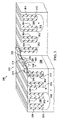
図7及び図8は、垂直のドレイン拡張されたMOSトランジスタを有する半導体デバイスの上面図である。図7及び図8に示すゲートは、図2を参照して説明したようにトレンチに配置されるが、これらの例においてゲートの他の構成も用いられ得る。図7を参照すると、半導体デバイス700が、図6Aを参照して説明したように半導体基板702内及び上に形成される。閉ループ構成を備えたディープトレンチ構造704が基板702に配置され得る。ディープトレンチ構造704のインスタンスが、垂直ドレインコンタクト領域706を横方向に囲む。垂直のドレイン拡張されたMOSトランジスタ710のゲート714及びゲート誘電体層716が、垂直ドレインコンタクト領域706を横方向に囲むディープトレンチ構造704間に配置される。垂直ドリフト領域708が、垂直ドレインコンタクト領域706を囲むディープトレンチ構造704間に配置される。垂直のドレイン拡張されたMOSトランジスタ710のボディ領域、ソース領域、及びボディコンタクト領域は、垂直ドリフト領域708及び垂直ドレインコンタクト領域706の配置をよりはっきりと示すために図7には示していない。ディープトレンチ構造704のインスタンスが、垂直のドレイン拡張されたMOSトランジスタ710を横方向に囲む。垂直ドレインコンタクト領域706への電気的接続は、基板702の頂部表面において成される。垂直ドレインコンタクト領域706をディープトレンチ構造704で囲むことが、垂直のドレイン拡張されたMOSトランジスタ710のドレインコンタクトとボディ領域との間のブレークダウン電界を防止し得、また、垂直のドレイン拡張されたMOSトランジスタ710を、その他の方式よりも高い電圧で有利に動作させ得る。
7 and 8 are top views of semiconductor devices having vertical drain extended MOS transistors. The gates shown in FIGS. 7 and 8 are disposed in the trenches as described with reference to FIG. 2, but other configurations of the gates may be used in these examples. Referring to FIG. 7, a
図8を参照すると、半導体デバイス800が、図6Aを参照して説明したように半導体基板802内及び上に形成される。線形構成を備えたディープトレンチ構造804が基板802に配置され得る。垂直ドレインコンタクト領域806が、線形ディープトレンチ構造804の隣り合う対の間に配置される。ゲート814及びゲート誘電体層816が、垂直ドレインコンタクト領域806と互い違いに、ディープトレンチ構造804の隣り合う対の間に配置される。垂直ドリフト領域808が、ゲート814を備えたディープトレンチ構造804の互い違いの対の間に配置される。ボディ領域818が、線形ディープトレンチ構造804の周りに配置され、ゲート814に隣接するように垂直ドリフト領域808の上に延在する。この場合、垂直ドリフト領域808の上に延在するボディ領域818の一部と、垂直のドレイン拡張されたMOSトランジスタ810のソース領域及びボディコンタクト領域は、垂直ドリフト領域808及び垂直ドレインコンタクト領域806の配置をよりはっきりと示すために図8には示していない。ディープトレンチ構造804のインスタンスが、垂直のドレイン拡張されたMOSトランジスタ810を横方向に囲む。垂直ドレインコンタクト領域806への電気的接続は、基板802の頂部表面において成される。線形ディープトレンチ構造804間に垂直ドレインコンタクト領域806を配置することが、垂直のドレイン拡張されたMOSトランジスタ810のために必要とされるエリアを有利に低減し得、それにより、半導体デバイス800の製造コストを低減する。
Referring to FIG. 8, a
本発明の特許請求の範囲内で、説明した例示の実施例に変形が成され得、多くの他の実施例が可能である。 Within the scope of the claims of the invention, variations may be made to the exemplary embodiments described and many other embodiments are possible.
Claims (9)
前記半導体基板の表面に形成され、側壁と底部を有するゲートトレンチであって、前記側壁と前記底部の上にゲート誘電層が形成され、前記ゲート誘電層の上にゲートが形成される、前記ゲートトレンチと、A gate trench formed on a surface of the semiconductor substrate and having a sidewall and a bottom, wherein a gate dielectric layer is formed on the sidewall and the bottom, and a gate is formed on the gate dielectric layer. Trenches,
前記基板の前記表面に形成され、前記ゲートトレンチの前記側壁に隣接する第一の導電型のソース領域と、A source region of a first conductivity type formed on the surface of the substrate and adjacent to the sidewall of the gate trench;
前記基板の中で前記ソース領域の下に形成され、前記ゲートトレンチの前記側壁に隣接する第二の導電型のボディ領域と、A body region of a second conductivity type formed below the source region in the substrate and adjacent to the sidewall of the gate trench;
前記基板の中で前記ボディ領域の下に形成される前記第一の導電型のドリフト領域と、A drift region of the first conductivity type formed under the body region in the substrate;
前記基板の前記表面に形成される第一の閉ループ構成のトレンチであって、前記第一の閉ループ構成のトレンチは側壁と底部を有し、さらに、前記第一の閉ループ構成のトレンチの前記側壁と前記底部の上に形成される第一の誘電体ライナーと、前記第一の誘電体ライナーの上に形成され、かつ、前記ソース領域に電気的に接続される第一の導電性部材とを有する、前記第一の閉ループ構成のトレンチと、A first closed-loop trench formed on the surface of the substrate, the first closed-loop trench having side walls and a bottom; and the first closed-loop trench side wall; A first dielectric liner formed on the bottom; and a first conductive member formed on the first dielectric liner and electrically connected to the source region. A trench in the first closed loop configuration;
前記基板の前記表面に形成される第二の閉ループ構成のトレンチであって、前記第二の閉ループ構成のトレンチは側壁と底部を有し、さらに、前記第二の閉ループ構成のトレンチの前記側壁と前記底部の上に形成された第二の誘電体ライナーと、前記第二の誘電体ライナーの上に形成され、かつ、前記ソース領域に電気的に接続される第二の導電性部材とを有する、前記第二の閉ループ構成のトレンチと、A second closed-loop configuration trench formed on the surface of the substrate, the second closed-loop configuration trench having a side wall and a bottom; and the second closed-loop configuration trench side wall A second dielectric liner formed on the bottom; and a second conductive member formed on the second dielectric liner and electrically connected to the source region. A trench in the second closed loop configuration;
を含む、縦型MOSトランジスタであって、A vertical MOS transistor including
前記ゲートトレンチは前記第一の閉ループ構成のトレンチと前記第二の閉ループ構成のトレンチの間に配置され、The gate trench is disposed between the first closed-loop configuration trench and the second closed-loop configuration trench;
前記ソース領域の第一の部分は前記ゲートトレンチの前記側壁と前記第一の閉ループ構成のトレンチの前記側壁の間の全体に延在し、A first portion of the source region extends entirely between the sidewall of the gate trench and the sidewall of the trench in the first closed loop configuration;
前記ソース領域の第二の部分は前記ゲートトレンチの前記側壁と前記第二の閉ループ構成のトレンチの前記側壁の間の全体に延在する、縦型MOSトランジスタ。A vertical MOS transistor, wherein the second portion of the source region extends entirely between the sidewall of the gate trench and the sidewall of the second closed loop trench.
前記二つの閉ループ構成のトレンチの内部領域が、前記第一の導電型を有し、ドレインコンタクトを形成する、縦型MOSトランジスタ。A vertical MOS transistor, wherein an inner region of the two closed-loop trenches has the first conductivity type and forms a drain contact.
前記第一の閉ループ構成のトレンチと前記第二の閉ループ構成のトレンチの深さが、1μmから5μmの間の値をとる、縦型MOSトランジスタ。A vertical MOS transistor, wherein a depth of the first closed-loop configuration trench and the second closed-loop configuration trench takes a value between 1 μm and 5 μm.
前記第一の閉ループ構成のトレンチと前記第二の閉ループ構成のトレンチの幅が、0.5μmから1.5μmの間の値をとる、縦型MOSトランジスタ。A vertical MOS transistor, wherein a width of the first closed-loop trench and the second closed-loop trench is between 0.5 μm and 1.5 μm.
前記第一の誘電体ライナーと第二の誘電体ライナーがシリコン窒化物を含む、縦型MOSトランジスタ。A vertical MOS transistor, wherein the first dielectric liner and the second dielectric liner include silicon nitride.
前記第一の誘電体ライナーと第二の誘電体ライナーがシリコンオキシナイトライドを含む、縦型MOSトランジスタ。A vertical MOS transistor, wherein the first dielectric liner and the second dielectric liner contain silicon oxynitride.
前記半導体基板の前記表面に形成され、側壁と底部を有する第二のゲートトレンチであって、前記第二のゲートトレンチの前記側壁と前記底部の上に第二のゲート誘電層が形成され、前記第二のゲート誘電層の上に第二のゲートが形成される、前記第二のゲートトレンチをさらに含み、A second gate trench formed on the surface of the semiconductor substrate and having a sidewall and a bottom, wherein a second gate dielectric layer is formed on the sidewall and the bottom of the second gate trench; Further comprising the second gate trench, wherein a second gate is formed over the second gate dielectric layer;
前記第二のゲートトレンチは前記第一の閉ループ構成のトレンチと前記第二の閉ループ構成のトレンチの間に配置され、The second gate trench is disposed between the first closed-loop configuration trench and the second closed-loop configuration trench;
前記ソース領域の第三の部分は前記第二のゲートトレンチの前記側壁と前記第一の閉ループ構成のトレンチの前記側壁の間の全体に延在し、A third portion of the source region extends entirely between the sidewall of the second gate trench and the sidewall of the trench in the first closed loop configuration;
前記ソース領域の第四の部分は前記第二のゲートトレンチの前記側壁と前記第二の閉ループ構成のトレンチの前記側壁の間の全体に延在する、縦型MOSトランジスタ。The fourth portion of the source region extends vertically between the sidewall of the second gate trench and the sidewall of the second closed loop trench.
前記基板の前記表面に形成される第三の閉ループ構成のトレンチであって、前記第三の閉ループ構成のトレンチは側壁と底部を有し、さらに、前記第三の閉ループ構成のトレンチの前記側壁と前記底部の上に形成される第三の誘電体ライナーと、前記第三の誘電体ライナーの上に形成され、かつ、前記ソース領域に電気的に接続される第三の導電性部材とを有する、前記第三の閉ループ構成のトレンチと、A third closed-loop trench formed on the surface of the substrate, the third closed-loop trench having side walls and a bottom; and the third closed-loop trench side wall; A third dielectric liner formed on the bottom; and a third conductive member formed on the third dielectric liner and electrically connected to the source region. The third closed loop trench;
前記半導体基板の前記表面に形成され、側壁と底部を有する第二のゲートトレンチであって、前記第二のゲートトレンチの前記側壁と前記底部の上に第二のゲート誘電層が形成され、前記第二のゲート誘電層の上に第二のゲートが形成される、前記第二のゲートトレンチと、A second gate trench formed on the surface of the semiconductor substrate and having a sidewall and a bottom, wherein a second gate dielectric layer is formed on the sidewall and the bottom of the second gate trench; The second gate trench, wherein a second gate is formed on the second gate dielectric layer; and
をさらに含み、Further including
前記第二のゲートトレンチは前記第二の閉ループ構成のトレンチと前記第三の閉ループ構成のトレンチの間に配置され、The second gate trench is disposed between the second closed-loop configuration trench and the third closed-loop configuration trench;
前記ソース領域の第三の部分は前記第二のゲートトレンチの前記側壁と前記第二の閉ループ構成のトレンチの前記側壁の間の全体に延在し、A third portion of the source region extends entirely between the sidewall of the second gate trench and the sidewall of the trench in the second closed loop configuration;
前記ソース領域の第四の部分は前記第二のゲートトレンチの前記側壁と前記第三の閉ループ構成のトレンチの前記側壁の間の全体に延在する、縦型MOSトランジスタ。The fourth portion of the source region extends vertically between the sidewall of the second gate trench and the sidewall of the third closed loop trench.
前記半導体基板の前記表面に形成され、側壁と底部を有する第三のゲートトレンチであって、前記第三のゲートトレンチの前記側壁と前記底部の上に第三のゲート誘電層が形成され、前記第三のゲート誘電層の上に第三のゲートが形成される、前記第三のゲートトレンチと、A third gate trench formed on the surface of the semiconductor substrate and having a sidewall and a bottom, wherein a third gate dielectric layer is formed on the sidewall and the bottom of the third gate trench; The third gate trench, wherein a third gate is formed on the third gate dielectric layer; and
前記半導体基板の前記表面に形成され、側壁と底部を有する第四のゲートトレンチであって、前記第四のゲートトレンチの前記側壁と前記底部の上に第四のゲート誘電層が形成され、前記第四のゲート誘電層の上に第四のゲートが形成される、前記第四のゲートトレンチと、A fourth gate trench formed on the surface of the semiconductor substrate and having a sidewall and a bottom, wherein a fourth gate dielectric layer is formed on the sidewall and the bottom of the fourth gate trench, The fourth gate trench, wherein a fourth gate is formed on the fourth gate dielectric layer; and
をさらに含み、Further including
前記第三のゲートトレンチは前記第一の閉ループ構成のトレンチと前記第二の閉ループ構成のトレンチの間に配置され、The third gate trench is disposed between the first closed-loop configuration trench and the second closed-loop configuration trench;
前記第四のゲートトレンチは前記第二の閉ループ構成のトレンチと前記第三の閉ループ構成のトレンチの間に配置され、The fourth gate trench is disposed between the second closed-loop configuration trench and the third closed-loop configuration trench;
前記ソース領域の第五の部分は前記第三のゲートトレンチの前記側壁と前記第一の閉ループ構成のトレンチの前記側壁の間の全体に延在し、A fifth portion of the source region extends entirely between the sidewall of the third gate trench and the sidewall of the trench in the first closed loop configuration;
前記ソース領域の第六の部分は前記第三のゲートトレンチの前記側壁と前記第二の閉ループ構成のトレンチの前記側壁の間の全体に延在し、A sixth portion of the source region extends entirely between the sidewall of the third gate trench and the sidewall of the trench in the second closed loop configuration;
前記ソース領域の第七の部分は前記第四のゲートトレンチの前記側壁と前記第二の閉ループ構成のトレンチの前記側壁の間の全体に延在し、A seventh portion of the source region extends entirely between the sidewall of the fourth gate trench and the sidewall of the trench in the second closed loop configuration;
前記ソース領域の第八の部分は前記第四のゲートトレンチの前記側壁と前記第三の閉ループ構成のトレンチの前記側壁の間の全体に延在する、縦型MOSトランジスタ。The eighth portion of the source region extends vertically between the sidewall of the fourth gate trench and the sidewall of the third closed loop trench.
Applications Claiming Priority (3)
| Application Number | Priority Date | Filing Date | Title |
|---|---|---|---|
| US14/044,909 US9136368B2 (en) | 2013-10-03 | 2013-10-03 | Trench gate trench field plate semi-vertical semi-lateral MOSFET |
| US14/044,909 | 2013-10-03 | ||
| PCT/US2014/057790 WO2015050790A1 (en) | 2013-10-03 | 2014-09-26 | Trench gate trench field plate semi-vertical semi-lateral mosfet |
Related Child Applications (1)
| Application Number | Title | Priority Date | Filing Date |
|---|---|---|---|
| JP2018135590A Division JP6763644B2 (en) | 2013-10-03 | 2018-07-19 | Trench Gate Trench Field Plate Semi-Vertical Semi-Horizontal MOSFET |
Publications (3)
| Publication Number | Publication Date |
|---|---|
| JP2016536782A JP2016536782A (en) | 2016-11-24 |
| JP2016536782A5 JP2016536782A5 (en) | 2018-04-19 |
| JP6374492B2 true JP6374492B2 (en) | 2018-08-15 |
Family
ID=52776280
Family Applications (5)
| Application Number | Title | Priority Date | Filing Date |
|---|---|---|---|
| JP2016520007A Active JP6374492B2 (en) | 2013-10-03 | 2014-09-26 | Trench Gate Trench Field Plate Semi-Vertical Semi-lateral MOSFET |
| JP2018135590A Active JP6763644B2 (en) | 2013-10-03 | 2018-07-19 | Trench Gate Trench Field Plate Semi-Vertical Semi-Horizontal MOSFET |
| JP2020105735A Active JP7021416B2 (en) | 2013-10-03 | 2020-06-19 | Trench Gate Trench Field Plate Semi-Vertical Semi-Horizontal MOSFET |
| JP2021201394A Active JP7397554B2 (en) | 2013-10-03 | 2021-12-13 | Trench gate trench field plate semi-vertical semi-lateral MOSFET |
| JP2023200041A Pending JP2024023411A (en) | 2013-10-03 | 2023-11-27 | Trench gate trench field plate semi-vertical semi-lateral MOSFET |
Family Applications After (4)
| Application Number | Title | Priority Date | Filing Date |
|---|---|---|---|
| JP2018135590A Active JP6763644B2 (en) | 2013-10-03 | 2018-07-19 | Trench Gate Trench Field Plate Semi-Vertical Semi-Horizontal MOSFET |
| JP2020105735A Active JP7021416B2 (en) | 2013-10-03 | 2020-06-19 | Trench Gate Trench Field Plate Semi-Vertical Semi-Horizontal MOSFET |
| JP2021201394A Active JP7397554B2 (en) | 2013-10-03 | 2021-12-13 | Trench gate trench field plate semi-vertical semi-lateral MOSFET |
| JP2023200041A Pending JP2024023411A (en) | 2013-10-03 | 2023-11-27 | Trench gate trench field plate semi-vertical semi-lateral MOSFET |
Country Status (6)
| Country | Link |
|---|---|
| US (2) | US9136368B2 (en) |
| EP (1) | EP3053194A4 (en) |
| JP (5) | JP6374492B2 (en) |
| CN (2) | CN105793987B (en) |
| DE (1) | DE202014011171U1 (en) |
| WO (1) | WO2015050790A1 (en) |
Families Citing this family (4)
| Publication number | Priority date | Publication date | Assignee | Title |
|---|---|---|---|---|
| US9385187B2 (en) * | 2014-04-25 | 2016-07-05 | Texas Instruments Incorporated | High breakdown N-type buried layer |
| US10217821B2 (en) * | 2014-09-01 | 2019-02-26 | Sk Hynix System Ic Inc. | Power integrated devices, electronic devices and electronic systems including the same |
| CN107785273B (en) * | 2016-08-31 | 2020-03-13 | 无锡华润上华科技有限公司 | Semiconductor device and method for manufacturing the same |
| US10826386B2 (en) * | 2018-10-26 | 2020-11-03 | Nxp B.V. | Multi-stage charge pump regulation architecture |
Family Cites Families (31)
| Publication number | Priority date | Publication date | Assignee | Title |
|---|---|---|---|---|
| JP3008480B2 (en) * | 1990-11-05 | 2000-02-14 | 日産自動車株式会社 | Semiconductor device |
| JPH06104446A (en) * | 1992-09-22 | 1994-04-15 | Toshiba Corp | Semiconductor device |
| US5365102A (en) * | 1993-07-06 | 1994-11-15 | North Carolina State University | Schottky barrier rectifier with MOS trench |
| CN1163973C (en) * | 1999-03-01 | 2004-08-25 | 通用半导体公司 | Trench DMOS transistor structure having low resistance path to drain contact located on upper surface |
| GB9917099D0 (en) * | 1999-07-22 | 1999-09-22 | Koninkl Philips Electronics Nv | Cellular trench-gate field-effect transistors |
| JP3704007B2 (en) * | 1999-09-14 | 2005-10-05 | 株式会社東芝 | Semiconductor device and manufacturing method thereof |
| US6812526B2 (en) * | 2000-03-01 | 2004-11-02 | General Semiconductor, Inc. | Trench DMOS transistor structure having a low resistance path to a drain contact located on an upper surface |
| US6593620B1 (en) * | 2000-10-06 | 2003-07-15 | General Semiconductor, Inc. | Trench DMOS transistor with embedded trench schottky rectifier |
| US6586833B2 (en) * | 2000-11-16 | 2003-07-01 | Silicon Semiconductor Corporation | Packaged power devices having vertical power mosfets therein that are flip-chip mounted to slotted gate electrode strip lines |
| US6657254B2 (en) * | 2001-11-21 | 2003-12-02 | General Semiconductor, Inc. | Trench MOSFET device with improved on-resistance |
| RU2230394C1 (en) * | 2002-10-11 | 2004-06-10 | ОАО "ОКБ "Искра" | Bipolar combined-gate field-effect transistor |
| GB0407012D0 (en) * | 2004-03-27 | 2004-04-28 | Koninkl Philips Electronics Nv | Trench insulated gate field effect transistor |
| JP4721653B2 (en) | 2004-05-12 | 2011-07-13 | トヨタ自動車株式会社 | Insulated gate semiconductor device |
| JP4414863B2 (en) | 2004-10-29 | 2010-02-10 | トヨタ自動車株式会社 | Insulated gate semiconductor device and manufacturing method thereof |
| JP4692313B2 (en) * | 2006-02-14 | 2011-06-01 | トヨタ自動車株式会社 | Semiconductor device |
| JP4453671B2 (en) | 2006-03-08 | 2010-04-21 | トヨタ自動車株式会社 | Insulated gate semiconductor device and manufacturing method thereof |
| JP2009531850A (en) * | 2006-03-28 | 2009-09-03 | エヌエックスピー ビー ヴィ | Trench gate semiconductor device and manufacturing method thereof |
| JP5157164B2 (en) | 2006-05-29 | 2013-03-06 | 富士電機株式会社 | Semiconductor device, battery protection circuit and battery pack |
| US8653583B2 (en) | 2007-02-16 | 2014-02-18 | Power Integrations, Inc. | Sensing FET integrated with a high-voltage transistor |
| US7557406B2 (en) * | 2007-02-16 | 2009-07-07 | Power Integrations, Inc. | Segmented pillar layout for a high-voltage vertical transistor |
| DE102007014038B4 (en) * | 2007-03-23 | 2015-02-12 | Infineon Technologies Austria Ag | Method for producing a semiconductor component |
| KR100861213B1 (en) * | 2007-04-17 | 2008-09-30 | 동부일렉트로닉스 주식회사 | Semiconductor device and method for manufactruing of the same |
| JP2009135360A (en) * | 2007-12-03 | 2009-06-18 | Renesas Technology Corp | Semiconductor device and its manufacturing method |
| US8519473B2 (en) * | 2010-07-14 | 2013-08-27 | Infineon Technologies Ag | Vertical transistor component |
| US9396997B2 (en) * | 2010-12-10 | 2016-07-19 | Infineon Technologies Ag | Method for producing a semiconductor component with insulated semiconductor mesas |
| US9443972B2 (en) * | 2011-11-30 | 2016-09-13 | Infineon Technologies Austria Ag | Semiconductor device with field electrode |
| US9356133B2 (en) * | 2012-02-01 | 2016-05-31 | Texas Instruments Incorporated | Medium voltage MOSFET device |
| US8796760B2 (en) * | 2012-03-14 | 2014-08-05 | Taiwan Semiconductor Manufacturing Company, Ltd. | Transistor and method of manufacturing the same |
| CN103681315B (en) * | 2012-09-18 | 2016-08-10 | 中芯国际集成电路制造(上海)有限公司 | The forming method of buried regions |
| US8860130B2 (en) * | 2012-11-05 | 2014-10-14 | Alpha And Omega Semiconductor Incorporated | Charged balanced devices with shielded gate trench |
| JP2013055347A (en) | 2012-11-08 | 2013-03-21 | Sanken Electric Co Ltd | Semiconductor device |
-
2013
- 2013-10-03 US US14/044,909 patent/US9136368B2/en active Active
-
2014
- 2014-09-26 JP JP2016520007A patent/JP6374492B2/en active Active
- 2014-09-26 EP EP14850568.8A patent/EP3053194A4/en not_active Withdrawn
- 2014-09-26 CN CN201480065667.8A patent/CN105793987B/en active Active
- 2014-09-26 DE DE202014011171.5U patent/DE202014011171U1/en active Active
- 2014-09-26 WO PCT/US2014/057790 patent/WO2015050790A1/en active Application Filing
- 2014-09-26 CN CN201911111690.7A patent/CN110808288B/en active Active
-
2015
- 2015-08-07 US US14/821,085 patent/US9240465B2/en active Active
-
2018
- 2018-07-19 JP JP2018135590A patent/JP6763644B2/en active Active
-
2020
- 2020-06-19 JP JP2020105735A patent/JP7021416B2/en active Active
-
2021
- 2021-12-13 JP JP2021201394A patent/JP7397554B2/en active Active
-
2023
- 2023-11-27 JP JP2023200041A patent/JP2024023411A/en active Pending
Also Published As
| Publication number | Publication date |
|---|---|
| JP2024023411A (en) | 2024-02-21 |
| US9240465B2 (en) | 2016-01-19 |
| CN105793987A (en) | 2016-07-20 |
| EP3053194A4 (en) | 2017-05-31 |
| JP7397554B2 (en) | 2023-12-13 |
| US20150097225A1 (en) | 2015-04-09 |
| JP2022033954A (en) | 2022-03-02 |
| US9136368B2 (en) | 2015-09-15 |
| CN110808288A (en) | 2020-02-18 |
| CN110808288B (en) | 2023-11-14 |
| EP3053194A1 (en) | 2016-08-10 |
| JP6763644B2 (en) | 2020-09-30 |
| DE202014011171U1 (en) | 2018-04-23 |
| WO2015050790A1 (en) | 2015-04-09 |
| JP2016536782A (en) | 2016-11-24 |
| JP2020161838A (en) | 2020-10-01 |
| CN105793987B (en) | 2019-11-22 |
| US20150349092A1 (en) | 2015-12-03 |
| JP2018201028A (en) | 2018-12-20 |
| JP7021416B2 (en) | 2022-02-17 |
Similar Documents
| Publication | Publication Date | Title |
|---|---|---|
| JP6492068B2 (en) | Vertical trench MOSFET devices in integrated power technology | |
| JP7397554B2 (en) | Trench gate trench field plate semi-vertical semi-lateral MOSFET | |
| US9269806B2 (en) | Semiconductor device and method of fabricating same | |
| CN103545370B (en) | Apparatus and method for power MOS transistor | |
| US11189721B2 (en) | Trench gate trench field plate vertical MOSFET | |
| JP5939846B2 (en) | Manufacturing method of semiconductor device | |
| JP2010199424A (en) | Semiconductor device, and manufacturing method of the same |
Legal Events
| Date | Code | Title | Description |
|---|---|---|---|
| A521 | Request for written amendment filed |
Free format text: JAPANESE INTERMEDIATE CODE: A523 Effective date: 20170915 |
|
| A621 | Written request for application examination |
Free format text: JAPANESE INTERMEDIATE CODE: A621 Effective date: 20170915 |
|
| A521 | Request for written amendment filed |
Free format text: JAPANESE INTERMEDIATE CODE: A523 Effective date: 20180308 |
|
| TRDD | Decision of grant or rejection written | ||
| A01 | Written decision to grant a patent or to grant a registration (utility model) |
Free format text: JAPANESE INTERMEDIATE CODE: A01 Effective date: 20180627 |
|
| A61 | First payment of annual fees (during grant procedure) |
Free format text: JAPANESE INTERMEDIATE CODE: A61 Effective date: 20180719 |
|
| R150 | Certificate of patent or registration of utility model |
Ref document number: 6374492 Country of ref document: JP Free format text: JAPANESE INTERMEDIATE CODE: R150 |
|
| S111 | Request for change of ownership or part of ownership |
Free format text: JAPANESE INTERMEDIATE CODE: R313117 |
|
| S533 | Written request for registration of change of name |
Free format text: JAPANESE INTERMEDIATE CODE: R313533 |
|
| R350 | Written notification of registration of transfer |
Free format text: JAPANESE INTERMEDIATE CODE: R350 |
|
| R360 | Written notification for declining of transfer of rights |
Free format text: JAPANESE INTERMEDIATE CODE: R360 |
|
| R250 | Receipt of annual fees |
Free format text: JAPANESE INTERMEDIATE CODE: R250 |
|
| R350 | Written notification of registration of transfer |
Free format text: JAPANESE INTERMEDIATE CODE: R350 |
|
| R250 | Receipt of annual fees |
Free format text: JAPANESE INTERMEDIATE CODE: R250 |