JP6371053B2 - Rectifier, alternator and power converter - Google Patents
Rectifier, alternator and power converter Download PDFInfo
- Publication number
- JP6371053B2 JP6371053B2 JP2013257733A JP2013257733A JP6371053B2 JP 6371053 B2 JP6371053 B2 JP 6371053B2 JP 2013257733 A JP2013257733 A JP 2013257733A JP 2013257733 A JP2013257733 A JP 2013257733A JP 6371053 B2 JP6371053 B2 JP 6371053B2
- Authority
- JP
- Japan
- Prior art keywords
- mosfet
- rectifier
- gate
- voltage
- current
- Prior art date
- Legal status (The legal status is an assumption and is not a legal conclusion. Google has not performed a legal analysis and makes no representation as to the accuracy of the status listed.)
- Active
Links
- 239000000872 buffer Substances 0.000 claims description 110
- 230000001360 synchronised effect Effects 0.000 claims description 51
- 230000000694 effects Effects 0.000 claims description 23
- 230000010355 oscillation Effects 0.000 claims description 13
- 238000004146 energy storage Methods 0.000 claims description 5
- 238000006243 chemical reaction Methods 0.000 claims 1
- 239000003990 capacitor Substances 0.000 description 49
- XUIMIQQOPSSXEZ-UHFFFAOYSA-N Silicon Chemical compound [Si] XUIMIQQOPSSXEZ-UHFFFAOYSA-N 0.000 description 41
- 229910052710 silicon Inorganic materials 0.000 description 41
- 239000010703 silicon Substances 0.000 description 41
- 244000145845 chattering Species 0.000 description 40
- 230000000052 comparative effect Effects 0.000 description 33
- 238000010586 diagram Methods 0.000 description 28
- 230000004048 modification Effects 0.000 description 21
- 238000012986 modification Methods 0.000 description 21
- 230000007257 malfunction Effects 0.000 description 15
- VYPSYNLAJGMNEJ-UHFFFAOYSA-N Silicium dioxide Chemical compound O=[Si]=O VYPSYNLAJGMNEJ-UHFFFAOYSA-N 0.000 description 8
- 239000004065 semiconductor Substances 0.000 description 8
- 229910052814 silicon oxide Inorganic materials 0.000 description 8
- 230000007704 transition Effects 0.000 description 6
- 239000004020 conductor Substances 0.000 description 5
- 238000010248 power generation Methods 0.000 description 5
- 230000000630 rising effect Effects 0.000 description 5
- 230000001629 suppression Effects 0.000 description 5
- 230000007423 decrease Effects 0.000 description 4
- 230000003111 delayed effect Effects 0.000 description 4
- 238000009499 grossing Methods 0.000 description 4
- 230000020169 heat generation Effects 0.000 description 4
- 229910021420 polycrystalline silicon Inorganic materials 0.000 description 4
- 229920005591 polysilicon Polymers 0.000 description 4
- 230000004044 response Effects 0.000 description 4
- 230000002441 reversible effect Effects 0.000 description 4
- 239000000758 substrate Substances 0.000 description 4
- 230000008859 change Effects 0.000 description 3
- 238000004519 manufacturing process Methods 0.000 description 3
- 230000006870 function Effects 0.000 description 2
- 238000000034 method Methods 0.000 description 2
- 238000010521 absorption reaction Methods 0.000 description 1
- 230000003321 amplification Effects 0.000 description 1
- 230000000295 complement effect Effects 0.000 description 1
- 230000005611 electricity Effects 0.000 description 1
- 230000005669 field effect Effects 0.000 description 1
- 230000008571 general function Effects 0.000 description 1
- 238000005286 illumination Methods 0.000 description 1
- 239000012212 insulator Substances 0.000 description 1
- 229910044991 metal oxide Inorganic materials 0.000 description 1
- 150000004706 metal oxides Chemical class 0.000 description 1
- 238000003199 nucleic acid amplification method Methods 0.000 description 1
- 230000003071 parasitic effect Effects 0.000 description 1
- 230000000149 penetrating effect Effects 0.000 description 1
- 230000035515 penetration Effects 0.000 description 1
- 230000002093 peripheral effect Effects 0.000 description 1
- 230000003252 repetitive effect Effects 0.000 description 1
- 238000004904 shortening Methods 0.000 description 1
- 230000001052 transient effect Effects 0.000 description 1
Images


Classifications
-
- H—ELECTRICITY
- H02—GENERATION; CONVERSION OR DISTRIBUTION OF ELECTRIC POWER
- H02M—APPARATUS FOR CONVERSION BETWEEN AC AND AC, BETWEEN AC AND DC, OR BETWEEN DC AND DC, AND FOR USE WITH MAINS OR SIMILAR POWER SUPPLY SYSTEMS; CONVERSION OF DC OR AC INPUT POWER INTO SURGE OUTPUT POWER; CONTROL OR REGULATION THEREOF
- H02M1/00—Details of apparatus for conversion
- H02M1/08—Circuits specially adapted for the generation of control voltages for semiconductor devices incorporated in static converters
-
- H—ELECTRICITY
- H02—GENERATION; CONVERSION OR DISTRIBUTION OF ELECTRIC POWER
- H02M—APPARATUS FOR CONVERSION BETWEEN AC AND AC, BETWEEN AC AND DC, OR BETWEEN DC AND DC, AND FOR USE WITH MAINS OR SIMILAR POWER SUPPLY SYSTEMS; CONVERSION OF DC OR AC INPUT POWER INTO SURGE OUTPUT POWER; CONTROL OR REGULATION THEREOF
- H02M7/00—Conversion of ac power input into dc power output; Conversion of dc power input into ac power output
- H02M7/02—Conversion of ac power input into dc power output without possibility of reversal
- H02M7/04—Conversion of ac power input into dc power output without possibility of reversal by static converters
- H02M7/12—Conversion of ac power input into dc power output without possibility of reversal by static converters using discharge tubes with control electrode or semiconductor devices with control electrode
- H02M7/21—Conversion of ac power input into dc power output without possibility of reversal by static converters using discharge tubes with control electrode or semiconductor devices with control electrode using devices of a triode or transistor type requiring continuous application of a control signal
- H02M7/217—Conversion of ac power input into dc power output without possibility of reversal by static converters using discharge tubes with control electrode or semiconductor devices with control electrode using devices of a triode or transistor type requiring continuous application of a control signal using semiconductor devices only
- H02M7/219—Conversion of ac power input into dc power output without possibility of reversal by static converters using discharge tubes with control electrode or semiconductor devices with control electrode using devices of a triode or transistor type requiring continuous application of a control signal using semiconductor devices only in a bridge configuration
-
- H—ELECTRICITY
- H03—ELECTRONIC CIRCUITRY
- H03K—PULSE TECHNIQUE
- H03K17/00—Electronic switching or gating, i.e. not by contact-making and –breaking
- H03K17/16—Modifications for eliminating interference voltages or currents
- H03K17/161—Modifications for eliminating interference voltages or currents in field-effect transistor switches
- H03K17/162—Modifications for eliminating interference voltages or currents in field-effect transistor switches without feedback from the output circuit to the control circuit
- H03K17/163—Soft switching
-
- H—ELECTRICITY
- H03—ELECTRONIC CIRCUITRY
- H03K—PULSE TECHNIQUE
- H03K17/00—Electronic switching or gating, i.e. not by contact-making and –breaking
- H03K17/30—Modifications for providing a predetermined threshold before switching
- H03K17/302—Modifications for providing a predetermined threshold before switching in field-effect transistor switches
-
- H—ELECTRICITY
- H02—GENERATION; CONVERSION OR DISTRIBUTION OF ELECTRIC POWER
- H02M—APPARATUS FOR CONVERSION BETWEEN AC AND AC, BETWEEN AC AND DC, OR BETWEEN DC AND DC, AND FOR USE WITH MAINS OR SIMILAR POWER SUPPLY SYSTEMS; CONVERSION OF DC OR AC INPUT POWER INTO SURGE OUTPUT POWER; CONTROL OR REGULATION THEREOF
- H02M1/00—Details of apparatus for conversion
- H02M1/0003—Details of control, feedback or regulation circuits
- H02M1/0029—Circuits or arrangements for limiting the slope of switching signals, e.g. slew rate
-
- H—ELECTRICITY
- H02—GENERATION; CONVERSION OR DISTRIBUTION OF ELECTRIC POWER
- H02M—APPARATUS FOR CONVERSION BETWEEN AC AND AC, BETWEEN AC AND DC, OR BETWEEN DC AND DC, AND FOR USE WITH MAINS OR SIMILAR POWER SUPPLY SYSTEMS; CONVERSION OF DC OR AC INPUT POWER INTO SURGE OUTPUT POWER; CONTROL OR REGULATION THEREOF
- H02M7/00—Conversion of ac power input into dc power output; Conversion of dc power input into ac power output
- H02M7/02—Conversion of ac power input into dc power output without possibility of reversal
- H02M7/04—Conversion of ac power input into dc power output without possibility of reversal by static converters
- H02M7/12—Conversion of ac power input into dc power output without possibility of reversal by static converters using discharge tubes with control electrode or semiconductor devices with control electrode
- H02M7/21—Conversion of ac power input into dc power output without possibility of reversal by static converters using discharge tubes with control electrode or semiconductor devices with control electrode using devices of a triode or transistor type requiring continuous application of a control signal
- H02M7/217—Conversion of ac power input into dc power output without possibility of reversal by static converters using discharge tubes with control electrode or semiconductor devices with control electrode using devices of a triode or transistor type requiring continuous application of a control signal using semiconductor devices only
- H02M7/219—Conversion of ac power input into dc power output without possibility of reversal by static converters using discharge tubes with control electrode or semiconductor devices with control electrode using devices of a triode or transistor type requiring continuous application of a control signal using semiconductor devices only in a bridge configuration
- H02M7/2195—Conversion of ac power input into dc power output without possibility of reversal by static converters using discharge tubes with control electrode or semiconductor devices with control electrode using devices of a triode or transistor type requiring continuous application of a control signal using semiconductor devices only in a bridge configuration the switches being synchronously commutated at the same frequency of the AC input voltage
-
- H—ELECTRICITY
- H03—ELECTRONIC CIRCUITRY
- H03K—PULSE TECHNIQUE
- H03K17/00—Electronic switching or gating, i.e. not by contact-making and –breaking
- H03K17/30—Modifications for providing a predetermined threshold before switching
- H03K2017/307—Modifications for providing a predetermined threshold before switching circuits simulating a diode, e.g. threshold zero
-
- Y—GENERAL TAGGING OF NEW TECHNOLOGICAL DEVELOPMENTS; GENERAL TAGGING OF CROSS-SECTIONAL TECHNOLOGIES SPANNING OVER SEVERAL SECTIONS OF THE IPC; TECHNICAL SUBJECTS COVERED BY FORMER USPC CROSS-REFERENCE ART COLLECTIONS [XRACs] AND DIGESTS
- Y02—TECHNOLOGIES OR APPLICATIONS FOR MITIGATION OR ADAPTATION AGAINST CLIMATE CHANGE
- Y02B—CLIMATE CHANGE MITIGATION TECHNOLOGIES RELATED TO BUILDINGS, e.g. HOUSING, HOUSE APPLIANCES OR RELATED END-USER APPLICATIONS
- Y02B70/00—Technologies for an efficient end-user side electric power management and consumption
- Y02B70/10—Technologies improving the efficiency by using switched-mode power supplies [SMPS], i.e. efficient power electronics conversion e.g. power factor correction or reduction of losses in power supplies or efficient standby modes
Landscapes
- Engineering & Computer Science (AREA)
- Power Engineering (AREA)
- Rectifiers (AREA)
- Power Conversion In General (AREA)
- Control Of Eletrric Generators (AREA)
Description
本発明は、自律型の同期整流MOSFET(Metal Oxide Semiconductor Field Effect Transistor)の整流装置と、この整流装置を用いたオルタネータおよび電力変換装置に関する。 The present invention relates to a rectifier of an autonomous synchronous rectifier MOSFET (Metal Oxide Semiconductor Field Effect Transistor), an alternator using the rectifier, and a power converter.
自動車にて発電を行うオルタネータには、整流素子としてこれまでダイオードが用いられてきた。ダイオードは安価ではあるが、順方向電圧降下があり、損失が大きい。これに対して、近年はダイオードに代わり、MOSFETがオルタネータ用の整流素子として使われ始めている。MOSFETを同期整流することにより、順方向電圧降下がなく0Vから順方向電流が立ち上がり、損失が少ない整流素子を実現可能である。 A diode has been used as a rectifying element in an alternator that generates electricity in an automobile. Although the diode is inexpensive, it has a forward voltage drop and a large loss. On the other hand, MOSFETs have recently started to be used as rectifiers for alternators instead of diodes. By synchronously rectifying the MOSFET, it is possible to realize a rectifying element with a low loss without a forward voltage drop and a forward current rising from 0V.
電源装置は、交流電力の周波数が一定である。よって、電源装置の整流素子としてMOSFETを用いる場合、クロックに同期させてMOSFETのオン・オフ制御を行うこともできる。しかし、オルタネータは、コイルで発電される交流電力の周波数が一定ではない。よって、オルタネータの整流素子としてMOSFETを用いる場合、電源装置等で用いる場合のように単にクロックに同期させるのではなく、その時々の周波数に同期させてMOSFETのオン・オフ制御を行う必要がある。
そこで、ホール素子を用いてモータの位置を検知してMOSFETの制御を行う方式が考えられるが、ホール素子を要するため、現状の整流素子をそのまま置き換えることができず、オルタネータを大きく変更しなければならない。
In the power supply device, the frequency of the AC power is constant. Therefore, when a MOSFET is used as the rectifying element of the power supply device, the on / off control of the MOSFET can be performed in synchronization with the clock. However, in the alternator, the frequency of the AC power generated by the coil is not constant. Therefore, when a MOSFET is used as the rectifier element of the alternator, it is necessary to perform on / off control of the MOSFET in synchronization with the frequency at that time, not simply in synchronization with the clock as in the case of use in a power supply device or the like.
Therefore, a method of controlling the MOSFET by detecting the position of the motor using a Hall element can be considered, but since the Hall element is required, the current rectifier cannot be replaced as it is, and the alternator must be changed greatly. Don't be.
特許文献1の請求項1には、「カソード端子(K1)、アノード端子(A1)および前記カソード端子と前記アノード端子の間に設けられている電子回路を備え、該電子回路には、逆ダイオード(Inversdiode)(D6)が組み込まれたMOSトランジスタ(T1)、コンデンサ(C1)および差動増幅器(T2,T3,R1,R2,R3)が含まれていることを特徴とする、整流器回路。」と記載されている。特許文献1の段落0018には、「整流器回路のカソード端子K1の電位が整流器回路のアノード端子A1の電位より正の極性にあり、その電位差がツェナダイオードD4によってセットされている値を超過すると、トランジスタT4,T5から成る電流増幅段の入力側の電位が上昇させられる。これによって、MOSトランジスタT1のゲートソース間の電圧も上昇し、MOSトランジスタT1のドレインとソースの間を電流が流れるようになる。」と記載されている。ここでは、特許文献1に記載された方式を自律型と呼ぶことにする。
自律型の同期整流MOSFETは、ホール素子等のセンサが不要であり、一般に制御回路も簡単であるために、オルタネータの整流部を安価に構成可能である。
Claim 1 of Patent Document 1 includes a “cathode terminal (K1), an anode terminal (A1), and an electronic circuit provided between the cathode terminal and the anode terminal. Rectifier circuit characterized in that it includes a MOS transistor (T1) incorporating an (Inversdiode) (D6), a capacitor (C1) and differential amplifiers (T2, T3, R1, R2, R3). It is described. Paragraph 0018 of Patent Document 1 states that “when the potential of the cathode terminal K1 of the rectifier circuit is more positive than the potential of the anode terminal A1 of the rectifier circuit and the potential difference exceeds the value set by the Zener diode D4, The potential on the input side of the current amplification stage composed of the transistors T4 and T5 is raised, whereby the voltage between the gate and source of the MOS transistor T1 also rises so that current flows between the drain and source of the MOS transistor T1. It becomes ". Here, the method described in Patent Document 1 is referred to as an autonomous type.
Since the autonomous synchronous rectification MOSFET does not require a sensor such as a Hall element and the control circuit is generally simple, the rectifier of the alternator can be configured at low cost.
特許文献2の段落0013には、「ターンオンの遷移期間の前半段階では、電圧駆動型素子のゲート電圧の立ち上がり速度が相対的に高速化され、ターンオンの遷移期間の後半段階では、電圧駆動型素子のゲート電圧の立ち上がり速度が相対的に低速化される。これにより、電圧駆動型素子がターンオンするときのスイッチング特性におけるトレードオフ関係が改善される。」と記載されている。この効果として段落0029には、「トランジスタTr1がターンオンするときのドレイン電流のサージ及びドレイン電流のリンギング現象が抑えられる。」と記載されている。
特許文献2の課題であるリンギング現象とは、スイッチング素子のオンとオフとの切り替え時に発生する振動のことをいう。リンギングは、高速にスイッチングした際にインダクタや基板の寄生容量などによって発生する現象である。
Paragraph 0013 of
The ringing phenomenon, which is a problem of
上記の自律型の同期整流MOSFETには安価に整流素子を提供できるメリットがあるが、MOSFETのオン・オフの誤判定を繰り返すチャタリングが起こりやすい、ノイズでMOSFETのオン・オフの誤動作を起こしやすいという問題がある。 The above-mentioned autonomous synchronous rectification MOSFET has the merit that it can provide a rectifying element at low cost, but chattering that repeats misjudgment of MOSFET on / off is likely to occur, and noise on / off malfunction of the MOSFET is likely to occur. There's a problem.
自律型の同期整流MOSFETでは、MOSFETのソース・ドレイン間の電圧を基にMOSFETのオン・オフの判定を行い、かつ、整流電流がMOSFETの内蔵ダイオードにも流れ、MOSFETに電流が流れている状態と内蔵ダイオードに電流が流れている状態とが切り替わるときにMOSFETのソース・ドレイン間の電圧が大きく変動するので、MOSFETのオン・オフの誤判定を繰り返すチャタリングが生じてしまう。また、MOSFETのソース・ドレイン間の電圧を基にMOSFETのオン・オフの判定を行うために、MOSFETのソースに接続された配線もしくはドレインに接続された配線にノイズがのると、そのノイズでMOSFETのソース・ドレイン間の電圧が変動し、MOSFETがオン・オフの誤動作を起こしてしまう。 In autonomous synchronous rectification MOSFET, it is determined whether the MOSFET is on or off based on the voltage between the source and drain of the MOSFET, and the rectification current also flows through the built-in diode of the MOSFET, and the current is flowing through the MOSFET. Since the voltage between the source and drain of the MOSFET fluctuates greatly when the current is flowing through the built-in diode, chattering that repeatedly makes erroneous determinations of ON / OFF of the MOSFET occurs. In addition, in order to determine whether the MOSFET is on or off based on the voltage between the source and drain of the MOSFET, if noise is applied to the wiring connected to the source of the MOSFET or the wiring connected to the drain, the noise The voltage between the source and drain of the MOSFET fluctuates, causing the MOSFET to malfunction on and off.
オルタネータに自律型の同期整流MOSFETを使う場合、広い温度範囲、広い発電交流電力の周波数、広い出力電流、変動するバッテリ電圧という条件で、正しく自律型の制御を行わなければならない。このような広い条件において、同様の自律型の制御を行うことは難しい。また、オルタネータの発電交流電力の周波数は、範囲が広いだけでなく、数十Hz〜数kHz程度と低い。発電交流電力の周波数が低いと、ソース・ドレイン間の電圧の時間変化が遅くなり、オンもしくはオフの切り替えに時間を要してしまうために、上記チャタリングが生じやすい。 When an autonomous synchronous rectification MOSFET is used as an alternator, autonomous control must be correctly performed under the conditions of a wide temperature range, a wide frequency of generated AC power, a wide output current, and a fluctuating battery voltage. It is difficult to perform similar autonomous control under such a wide range of conditions. Further, the frequency of the generated AC power of the alternator is not only wide, but is as low as about several tens Hz to several kHz. When the frequency of the generated AC power is low, the time change of the voltage between the source and the drain becomes slow, and it takes time to switch on or off, so that the chattering is likely to occur.
なお、特許文献2は、第1実施形態(段落0029および図3)に記載されているように、「ターンオンの遷移期間の前半段階におけるゲート電圧の立ち上がり速度が相対的に高速化されており、ターンオンの遷移期間の後半段階におけるゲート電圧の立ち上がり速度が相対的に低速化されている。」構成を開示するものである。そのため、例えば仮に、ターンオフの遷移期間を前半・後半共に速いままの構成とすれば、前半と後半とを合わせたターンオンの速度が前半と後半とを合わせたターンオフの速度より遅くなる場合があると考えられることから、一見すると、MOSFETのゲートをオフする速度よりオンする速度の方が遅い構成が同文献に開示されているかのように見える。
Note that, as described in the first embodiment (paragraph 0029 and FIG. 3),
しかし、特許文献2の課題は、段落0012に記載されているように、「電圧駆動型素子のターンオン又はターンオフの遷移期間が高速化された場合でも、スイッチング特性におけるトレードオフ関係を改善すること」である。つまり、特許文献2に記載の発明は、スイッチング動作が高速であることを前提としている。上記のトレードオフ関係とは、特許文献2の段落0006に記載されており、スイッチング損失とサージとの関係およびスイッチング損失とリンギングとの関係のことをいう。ターンオンする速度を遅くすることで改善するサージおよびリンギングは、スイッチングの速度が速い場合に特に課題となるものである。また、特許文献2は、MOSFETのソース・ドレイン間の電圧を基にMOSFETのオン・オフの判定を行う「自律型」を構成要素とした発明を一切開示していない。
一方、本発明が解決するチャタリング抑制は、オルタネータに用いられるときのように、スイッチングの速度が遅い場合に特に課題となるものである。また、本発明が目的とするチャタリング抑制やノイズ印加時の貫通電流の抑止は、自律型の制御を行うことによって生じる解決課題である。したがって、特許文献2に記載の発明は、本発明が目的とするチャタリング抑制や、ノイズ印加時の貫通電流の抑止を解決課題とするものではなく、特許文献2に記載の発明と本願発明とは、根本的に異なる発明であることに留意すべきである。
However, as described in paragraph 0012, the problem of
On the other hand, chattering suppression solved by the present invention is a particular problem when the switching speed is low, such as when used in an alternator. In addition, the suppression of chattering and the suppression of the through current at the time of applying noise, which are the object of the present invention, are solution problems caused by autonomous control. Therefore, the invention described in
本発明は、チャタリングを防止し、ノイズ印加時の誤動作で貫通電流が流れることを防止することが可能な自律型の同期整流MOSFETの整流装置と、この整流装置を用いたオルタネータおよび電力変換装置を提供することを課題とする。 The present invention relates to an autonomous type synchronous rectification MOSFET rectifier capable of preventing chattering and preventing a through current from flowing due to a malfunction during application of noise, and an alternator and a power converter using the rectifier. The issue is to provide.
上記した課題を解決するため、第1の発明の整流装置は、同期整流を行う整流MOSFETと、前記整流MOSFETの一対の主端子間の電圧を入力し、入力した前記一対の主端子間の電圧に基づいて前記整流MOSFETのオン・オフを判定する判定回路と、前記判定回路の判定結果により前記整流MOSFETのゲートのオン・オフを行い、前記整流MOSFETをオフするときにゲート電圧の降圧に要する時間よりも前記整流MOSFETをオンするときにゲート電圧の昇圧に要する時間を長くして、前記判定回路の判定結果がチャタリングした際にフイルタ効果によりゲート電圧の振動を抑制するように構成されるゲート駆動回路とを備える。前記ゲート駆動回路は、ハイ側MOSFETおよびロウ側MOSFETを備えて、出力が前記整流MOSFETのゲートに接続される第1のCMOSバッファと、出力が前記第1のCMOSバッファの入力に接続された第2のCMOSバッファとを含んで構成される。前記整流MOSFETをオンするときに前記第1のCMOSバッファのハイ側MOSFETに流れる電流は、前記整流MOSFETをオフするときに前記第1のCMOSバッファのロウ側MOSFETに流れる電流よりも小さく、前記整流MOSFETをオンするときに前記第2のCMOSバッファのロウ側MOSFETに流れる電流は、前記整流MOSFETをオフするときに前記第2のCMOSバッファのハイ側MOSFETに流れる電流よりも小さい。
第2の発明の整流装置は、同期整流を行う整流MOSFETと、前記整流MOSFETの一対の主端子間の電圧を入力し、入力した前記一対の主端子間の電圧に基づいて前記整流MOSFETのオン・オフを判定する判定回路と、前記判定回路の判定結果により前記整流MOSFETのゲートのオン・オフを行い、前記整流MOSFETをオフするときにゲート電圧の降圧に要する時間よりも前記整流MOSFETをオンするときにゲート電圧の昇圧に要する時間を長くして、前記判定回路の判定結果がチャタリングした際にフイルタ効果によりゲート電圧の振動を抑制するように構成されるゲート駆動回路とを備える。
前記ゲート駆動回路は、ハイ側MOSFETおよびロウ側MOSFETを備えて、出力が前記整流MOSFETのゲートに接続される第1のCMOSバッファを含んで構成される。前記第1のCMOSバッファは、ハイ側MOSFETのゲート幅をゲート長で除算した商よりも、ロウ側MOSFETのゲート幅をゲート長で除算した商の2倍の方が大きくなるように構成される。前記整流MOSFETをオンするときに前記第1のCMOSバッファのハイ側MOSFETに流れる電流は、前記整流MOSFETをオフするときに前記第1のCMOSバッファのロウ側MOSFETに流れる電流よりも小さい。
In order to solve the above-described problem, a rectifier according to a first aspect of the present invention inputs a voltage between a pair of main terminals of a rectification MOSFET that performs synchronous rectification and a pair of main terminals of the rectification MOSFET. A determination circuit that determines whether the rectification MOSFET is turned on or off based on the determination circuit, and a gate voltage of the rectification MOSFET that is turned on / off based on a determination result of the determination circuit. by increasing the time required to boost the gate voltage when turning on the rectifier MOSFET than the time, the gate configured to suppress so the vibration of the gate voltage by the filter effect determination result upon chattering of the decision circuit And a drive circuit. The gate drive circuit includes a high-side MOSFET and a low-side MOSFET, and has a first CMOS buffer whose output is connected to the gate of the rectifier MOSFET, and an output whose first output is connected to the input of the first CMOS buffer. 2 CMOS buffers. The current flowing through the high-side MOSFET of the first CMOS buffer when the rectifying MOSFET is turned on is smaller than the current flowing through the low-side MOSFET of the first CMOS buffer when the rectifying MOSFET is turned off. The current that flows through the low-side MOSFET of the second CMOS buffer when the MOSFET is turned on is smaller than the current that flows through the high-side MOSFET of the second CMOS buffer when the rectifier MOSFET is turned off.
According to a second aspect of the present invention, a rectifier MOSFET that performs synchronous rectification and a voltage between a pair of main terminals of the rectifier MOSFET are input, and the rectifier MOSFET is turned on based on the input voltage between the pair of main terminals. A determination circuit for determining the off state, and the gate of the rectification MOSFET is turned on / off based on the determination result of the determination circuit, and the rectification MOSFET is turned on more than the time required for stepping down the gate voltage when the rectification MOSFET is turned off. A gate drive circuit configured to suppress the oscillation of the gate voltage by a filter effect when the time required for boosting the gate voltage is lengthened and the determination result of the determination circuit is chattered.
The gate drive circuit includes a high-side MOSFET and a low-side MOSFET, and includes a first CMOS buffer whose output is connected to the gate of the rectifier MOSFET. The first CMOS buffer is configured such that twice the quotient obtained by dividing the gate width of the low-side MOSFET by the gate length is larger than the quotient obtained by dividing the gate width of the high-side MOSFET by the gate length. . The current that flows through the high-side MOSFET of the first CMOS buffer when the rectifying MOSFET is turned on is smaller than the current that flows through the low-side MOSFET of the first CMOS buffer when the rectifying MOSFET is turned off.
第3の発明のオルタネータは、直流端子がバッテリに、交流端子が交流電源に接続されるブリッジ型の整流回路と、前記整流回路のハイサイドおよびロウサイドにそれぞれ接続される前記整流装置とを備える。 An alternator according to a third aspect of the present invention includes a bridge type rectifier circuit in which a DC terminal is connected to a battery and an AC terminal is connected to an AC power supply, and the rectifier connected to the high side and the low side of the rectifier circuit.
第4の発明の電力変換装置は、直流端子がエネルギ蓄積部に、交流端子が交流電源に接続されるブリッジ型の整流回路と、前記整流回路のハイサイドおよびロウサイドにそれぞれ接続される前記整流装置とを備える。
その他の手段については、発明を実施するための形態のなかで説明する。
According to a fourth aspect of the present invention, there is provided a power converter including a bridge type rectifier circuit in which a direct current terminal is connected to an energy storage unit, an alternating current terminal is connected to an alternating current power supply, and the rectifier connected to a high side and a low side of the rectifier circuit. With.
Other means will be described in the embodiment for carrying out the invention.
本発明によれば、チャタリングを防止し、ノイズ印加時の誤動作で貫通電流が流れることを防止する自律型の同期整流MOSFETの整流装置と、この整流装置を用いたオルタネータおよび電力変換装置を提供することが可能である。 According to the present invention, there is provided an autonomous type synchronous rectification MOSFET rectifier that prevents chattering and prevents a through current from flowing due to a malfunction during application of noise, and an alternator and a power converter using the rectifier. It is possible.
本発明の発明者らは、自律型の同期整流MOSFETの整流装置に、MOSFETのゲートをオフする速度よりオンする速度の方が遅いという構成を組み込むことによって、チャタリング抑制およびノイズ誤動作防止という効果が得られることを見出したものである。
以下、本発明の実施の形態を図面に基づいて詳細に説明する。なお、実施形態を説明するための各図において同一機能を有するものは同一の符号を付し、その繰り返しの説明は適宜省略する。また、以下の実施形態の説明では、特に必要なとき以外は同一又は同様な部分の説明は繰り返さずに適宜省略する。
The inventors of the present invention have the effect of suppressing chattering and preventing noise malfunction by incorporating a configuration in which the speed of turning on the gate of the MOSFET is slower than the speed of turning off the gate of the MOSFET in the rectifier of the autonomous synchronous rectifying MOSFET. It has been found that it can be obtained.
Hereinafter, embodiments of the present invention will be described in detail with reference to the drawings. Note that components having the same function are denoted by the same reference symbols in the drawings for describing the embodiments, and repetitive description thereof will be omitted as appropriate. In the following description of the embodiments, the description of the same or similar parts is not repeated and is appropriately omitted unless particularly necessary.
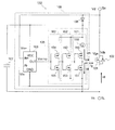
図1は、自律型の整流装置を用いたオルタネータの概略構成を示す回路図である。このオルタネータの構成は、比較例および各実施形態において共通する。
図1に示すように、自律型の同期整流MOSFETの整流装置132を用いたオルタネータ140は、回転子コイル109および固定子コイル110uv,110vw,110wuを含んで構成される発電部と、整流回路130とを備えている。
発電部は、回転子コイル109と、Δ結線された3本の固定子コイル110uv,110vw,110wuとを含んで構成される。固定子コイル110wu,110uvが結線されたノードからU相131uの中点配線が引き出される。固定子コイル110uv,110vwが結線されたノードからV相131vの中点配線が引き出される。固定子コイル110vw,110wuが結線されたノードからW相131wの中点配線が引き出される。なお、各固定子コイル110uv,110vw,110wuの結線は、Δ結線の代わりにY結線としてもよく、限定されない。
FIG. 1 is a circuit diagram showing a schematic configuration of an alternator using an autonomous rectifier. The configuration of this alternator is common to the comparative example and each embodiment.
As shown in FIG. 1, an alternator 140 using a
The power generation unit includes a
整流回路130は、U相131uとV相131vとW相131wとを含んで構成され、ノードNu,Nv,Nw間の三相交流を直流に整流してノードNp,Nn間(直流端子間)に流すものである。U相131uの中点配線のノードNuは、ハイサイド側に整流装置132uhが接続され、ロウサイド側に整流装置132ulが接続される。V相131vの中点配線のノードNvは、ハイサイド側に整流装置132vhが接続され、ロウサイド側に整流装置132vlが接続される。W相131wの中点配線のノードNwは、ハイサイド側に整流装置132whが接続され、ロウサイド側に整流装置132wlが接続される。ハイサイド側の整流装置132uh,132vh,132whは、直流の正極側のノードNpを通してバッテリ111(エネルギ蓄積部)の正極側端子が接続される。ロウサイド側の整流装置132ul,132vl,132wlは、直流の負極側のノードNnを通して、バッテリ111の負極側端子が接続される。
バッテリ111(エネルギ蓄積部)は、例えば車載用バッテリであり、その動作範囲は例えば10.8Vから14V程度である。
The
The battery 111 (energy storage unit) is, for example, a vehicle-mounted battery, and its operating range is, for example, about 10.8V to 14V.
U相131uのハイサイドの整流装置132uhは、整流MOSFET101uhと内蔵ダイオード102uhと制御IC(Integrated Circuit)108uhとコンデンサ107uhとを含んで構成される。U相131uのロウサイドの整流装置132ulは、同様に整流MOSFET101ulと内蔵ダイオード102ulと制御IC108ulとコンデンサ107ulとを含んで構成される。
V相131vのハイサイドの整流装置132vhは、整流MOSFET101vhと内蔵ダイオード102vhと制御IC108vhとコンデンサ107vhとを含んで構成される。V相131vのロウサイドの整流装置132vlは、同様に整流MOSFET101vlと内蔵ダイオード102vlと制御IC108vlとコンデンサ107vlとを含んで構成される。
The high-side rectifier 132uh of the
The V-
W相131wのハイサイドの整流装置132whは、整流MOSFET101whと内蔵ダイオード102whと制御IC108whとコンデンサ107whとを含んで構成される。W相131wのロウサイドの整流装置132wlは、同様に整流MOSFET101wlと内蔵ダイオード102wlと制御IC108wlとコンデンサ107wlとを含んで構成される。
なお、各相のロウサイドの整流装置132ul,132vl,132wlは、外部から制御IC108ul,108vl,108wlへの電源供給が容易なので、コンデンサ107ul,107vl,107wlを用いず、外部からの電源供給としてもよい。
以下、各整流装置132uh〜132wlを特に区別しないときには、比較例では整流装置132y,132zと記載し、各実施形態では整流装置132,132a〜132cと記載する。
各制御IC108uh〜108wlを特に区別しないときには、比較例では制御IC108y,108zと記載し、各実施形態では制御IC108、108a〜108cと記載する。
各整流MOSFET101uh〜101wlを特に区別しないときには、単に整流MOSFET101と記載する。各内蔵ダイオード102uh〜102wlを特に区別しないときには、単に内蔵ダイオード102と記載する。各コンデンサ107uh〜107wlを特に区別しないときには、単にコンデンサ107と記載する。
The high-side rectifier 132wh of the
The low-side rectifiers 132ul, 132vl, and 132wl of each phase can be supplied from the outside without using the capacitors 107ul, 107vl, and 107wl because the power supply to the control ICs 108ul, 108vl, and 108wl is easy from the outside. .
Hereinafter, when the rectifiers 132uh to 132wl are not particularly distinguished, they are described as
When the control ICs 108uh to 108wl are not particularly distinguished, they are described as
When the rectification MOSFETs 101uh to 101wl are not particularly distinguished, they are simply referred to as
図17は、第1比較例における自律型の同期整流MOSFETの整流装置132yを示す回路図である。
図17に示すように、整流装置132yは、整流MOSFET101と、整流MOSFET101のチップに内蔵される内蔵ダイオード102と、判定回路103と、ゲート駆動回路105yと、ダイオード106と、コンデンサ107とを含んで構成される。整流装置132yは、負極側主端子TLから正極側主端子THに電流を流すものである。
FIG. 17 is a circuit diagram showing a
As shown in FIG. 17, the
整流MOSFET101は、オルタネータ140の発電部が発電する大電流を流すため、パワーMOSFETが使用される。整流MOSFET101は、同期整流を行うものである。整流MOSFET101は、ドレインが正極側主端子THに接続され、ソースが負極側主端子TLに接続される。これにより整流MOSFET101の内蔵ダイオード102は、アノードが負極側主端子TLに接続され、カソードが正極側主端子THに接続される。
The
判定回路103は、非反転入力端子IN+が整流MOSFET101のドレインに接続され、反転入力端子IN−が整流MOSFET101のソースに接続される。判定回路103の出力端子OUTは、ゲート駆動回路105yの入力端子に接続される。判定回路103の出力端子OUTからは、比較信号Vcompが出力される。判定回路103は、一般的な機能を有するコンパレータでよく、非反転入力端子IN+の電圧Vin+と反転入力端子IN−の電圧Vin−とから比較信号Vcompを生成するものである。これにより判定回路103は、負極側主端子TLのソース電圧Vsと正極側主端子THのドレイン電圧Vdとの比較結果を出力する。判定回路103は、性能的には高精度ものが望ましい。
The
ダイオード106は、正極側主端子THからコンデンサ107の正極側端子への向きに接続される。コンデンサ107の正極側端子は、判定回路103とゲート駆動回路105yの電源電圧端子VCCに接続されて、直流電力を供給する。
ゲート駆動回路105yの出力端子は、整流MOSFET101のゲートに接続される。ゲート駆動回路105yは、ゲート電圧Vgsを出力する。ゲート駆動回路105yは、CMOS(Complementary MOS)バッファ161yを含んで構成される。CMOSバッファ161yは、ハイ側P型MOSFET150と、ロウ側N型MOSFET151とが直列接続された回路を含んで構成される。
The
The output terminal of the
制御IC108yは、判定回路103と、ゲート駆動回路105yと、ダイオード106とを含んで構成される。
コンデンサ107は、制御IC108yが駆動するための電源を供給するものである。コンデンサ107を電源に用いることで、整流装置132yの端子数は2個となり、オルタネータ140に用いられる従来の整流ダイオードの端子と互換性を持たせることができる。これにより、従来の整流ダイオードを整流装置132yに置き換えて、オルタネータ140の性能を向上可能である。
The
The
図1に示すオルタネータ140の各相のハイサイド側は、整流装置132yの正極側主端子THが、ノードNpを通してバッテリ111の正極側端子に接続される。整流装置132yの負極側主端子TLが、各相の中点配線であるノードNu,Nv,Nwに接続される。
各相のロウサイド側は、整流装置132yの正極側主端子THが、各相の中点配線であるノードNu,Nv,Nwに接続される。整流装置132yの負極側主端子TLが、ノードNnを通してバッテリ111の負極側端子に接続される。
On the high side of each phase of the alternator 140 shown in FIG. 1, the positive main terminal TH of the
On the low side of each phase, the positive side main terminal TH of the
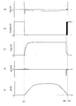
図18(a)〜(e)は、第1比較例における整流装置の各部波形を示すグラフ(その1)である。図18(a)〜(e)の横軸は、各グラフに共通する時間を示している。
図18は、U相131uのロウサイドに用いられている整流装置132ulの電圧および電流の波形を、ロウサイドの整流MOSFET101ulがオンしている期間に前後の期間を加えて示してある。以下、整流装置132ulは、単に整流装置132yと記載している場合がある。整流MOSFET101ulは、単に整流MOSFET101と記載している場合がある。
図18(a)は、整流MOSFET101のドレイン・ソース間電圧Vdsを示すグラフである。ドレイン・ソース間電圧Vdsは、判定回路103の非反転入力端子IN+と反転入力端子IN−との間に印加される電圧と同一である。判定回路103の非反転入力端子IN+は、正極側主端子THに接続されており、ドレイン電圧Vdが印加される。判定回路103の反転入力端子IN−は、負極側主端子TLに接続されており、ソース電圧Vsが印加される。
図18(b)は、判定回路103が出力する比較信号Vcompを示すグラフである。
図18(c)は、整流MOSFET101のゲート電圧Vgsを示すグラフである。ゲート電圧Vgsは、ゲート駆動回路105yの最終段のCMOSバッファ161yの出力電圧でもある。
図18(d)は、ゲート駆動回路105yから整流MOSFET101のゲートに向けて流れるゲート電流Igを示すグラフである。
図18(e)は、整流MOSFET101のドレイン電流Idを示すグラフである。このドレイン電流Idは、整流電流である。
18A to 18E are graphs (No. 1) showing waveforms of respective parts of the rectifier in the first comparative example. The horizontal axes in FIGS. 18A to 18E show the time common to each graph.
FIG. 18 shows the voltage and current waveforms of the rectifier 132ul used on the low side of the U-phase 131u, with the periods before and after the period when the low-side rectifier MOSFET 101ul is on. Hereinafter, the rectifier 132ul may be simply referred to as the
FIG. 18A is a graph showing the drain-source voltage Vds of the rectifying
FIG. 18B is a graph showing the comparison signal Vcomp output from the
FIG. 18C is a graph showing the gate voltage Vgs of the rectifying
FIG. 18D is a graph showing the gate current Ig flowing from the
FIG. 18E is a graph showing the drain current Id of the rectifying
図18(a)〜(e)には、U相131uのロウサイドに用いられている整流装置132ulの電圧および電流の波形を示したが、U相131uのハイサイドに用いられている整流装置132uhの電圧および電流の波形も、整流素子の負極側主端子TLを基準にすれば同じ波形になる。V相131vやW相131wのロウサイドやハイサイドに用いられている各整流装置132yも同様である。
FIGS. 18A to 18E show the voltage and current waveforms of the rectifier 132ul used on the low side of the
第1比較例の自律型の同期整流MOSFETの整流装置132yを用いた整流回路の電圧および電流の波形を使って、自律型の同期整流MOSFETの整流装置132yの整流動作と、その課題を説明する。
第1比較例の自律型の同期整流MOSFETの整流装置132yで使われる制御IC108yは、最終段のCMOSバッファ161yは、チャネル長は同じで、ハイ側P型MOSFET150のチャネル幅がロウ側N型MOSFET151のチャネル幅の2倍であり、両者で飽和電流が同等になるような構成としている。
図18(a)〜(e)と、図19(a)〜(e)とは、整流MOSFET101をオフするタイミングが異なる。図18(a)〜(e)は、整流MOSFET101のドレイン電圧Vdがソース電圧Vsを上回った後で整流MOSFET101をオフにした場合を示している。図19(a)〜(e)は、オフのタイミングは早くなって整流MOSFET101のドレイン電圧Vdがソース電圧Vsを上回る前に整流MOSFET101をオフにした場合の波形である。
The rectification operation of the autonomous synchronous
The
18A to 18E and FIGS. 19A to 19E are different in timing for turning off the rectifying
図18(a)〜(e)に基づいて、自律型の同期整流MOSFETの整流動作を説明する。
オルタネータ140での発電は、固定子コイル110uv,110vw,110wuの中を回転子コイル109が回転することで行われる。このとき、各相のコイルには交流電力が発生し、その交流電力によって各相の中点配線の電圧が周期的に上下する。
The rectification operation of the autonomous synchronous rectification MOSFET will be described with reference to FIGS.
Power generation by the alternator 140 is performed by the
中点配線の電圧は、ロウサイドの整流素子の正極側主端子THの電圧と等しく、判定回路103の非反転入力端子IN+の電圧Vin+と等しい。
バッテリ111の負極側端子の電圧は、ロウサイドの整流素子の負極側主端子TLの電圧と等しく、判定回路103の反転入力端子IN−の電圧Vin−と等しい。
時刻t11において、中点配線の電圧がバッテリ111の負極側端子の電圧を下回る。すなわち、図18(a)に示すように、判定回路103の非反転入力端子IN+と反転入力端子IN−との間に印加されたドレイン・ソース間電圧Vdsが負になる。図18(b)に示すように、判定回路103の比較信号Vcompは、HレベルからLレベルへと変化する。
判定回路103の比較信号Vcompがゲート駆動回路105yに入力され、CMOSバッファ161yなどを伝わって出力される。これにより、図18(c)に示すように、ゲート電圧Vgsは昇圧する。最終段のCMOSバッファ161yなどのハイ側P型MOSFET150を通してドレイン電流Idhが流れて、図18(d)に示すように、ゲート電流Igが正方向に流れる。このゲート電流Igによって、図18(c)に示すように、整流MOSFET101のゲート電圧Vgsは昇圧する。ゲート電圧Vgsが上がると、整流MOSFET101がオン状態になり、図18(e)に示すように、ドレイン電流Idが流れて整流が開始される。このあと時刻t11〜t12の間、比較信号Vcompはチャタリングする。
時刻t12において、比較信号VcompはLレベルで安定し、チャタリングは終了する。その後、中点配線の電圧は、下降したのち上昇に転じる。
The voltage of the midpoint wiring is equal to the voltage of the positive main terminal TH of the low-side rectifier element, and is equal to the voltage Vin + of the non-inverting input terminal IN + of the
The voltage at the negative terminal of the
At time t <b> 11, the voltage at the midpoint wiring is lower than the voltage at the negative terminal of the
The comparison signal Vcomp of the
At time t12, the comparison signal Vcomp becomes stable at the L level, and chattering ends. Thereafter, the voltage of the midpoint wiring starts to rise and then rises.
時刻t13において、中点配線の電圧は、バッテリ111の負極側端子の電圧を上回る。判定回路103の非反転入力端子IN+の電圧Vin+が反転入力端子IN−の電圧Vin−を上回る。図18(a)に示すように、ドレイン・ソース間電圧Vdsが負になる。これにより、図18(b)に示すように、判定回路103が出力する比較信号Vcompは、LレベルからHレベルへと変化する。
判定回路103が出力する比較信号Vcompがゲート駆動回路105に入力され、CMOSバッファ161yなどを伝わって出力される。これにより、図18(c)に示すように、ゲート電圧Vgsは降圧する。最終段のCMOSバッファ161yなどのロウ側N型MOSFET151を通してドレイン電流Idlが流れ、図18(d)に示すように、ゲート電流Igが逆方向に流れる。このゲート電流Igによって、図18(c)に示すように、ゲート電圧Vgsは降圧する。ゲート電圧Vgsが下がると、整流MOSFET101はオフ状態になり、図18(e)に示すように、ドレイン電流Idは流れなくなり、当該周期における整流動作が終了する。
At time t <b> 13, the voltage at the midpoint wiring exceeds the voltage at the negative terminal of the
The comparison signal Vcomp output from the
続いて、第1比較例の自律型の同期整流MOSFETの課題を説明する。
時刻t11において、整流動作を開始するとき、整流MOSFET101のドレイン電圧Vdがソース電圧Vsを下回ったのちに、判定回路103とゲート駆動回路105yとが動作する。整流電流であるドレイン電流Idが流れ始める時点で、整流MOSFET101はオフ状態であり、最初に内蔵ダイオード102に整流電流が流れる。整流装置132yのオン電圧は、正極側主端子THと負極側主端子TLとの間の電圧であり、ここに高抵抗の内蔵ダイオード102で決まる大きな電圧が現れる。
その後、制御IC108yが動作して整流MOSFET101がオン状態になると、整流電流は低抵抗の整流MOSFET101を流れる。整流装置132yのオン電圧は、整流MOSFET101の低いオン抵抗で決まる電圧へと急激に小さくなる。整流装置132yのオン電圧が小さくなるので、再度整流MOSFET101がオフする判定基準を満たして整流MOSFET101はオフ状態となる。整流MOSFET101がオフするので、内蔵ダイオード102に電流が流れ、整流装置132yのオン電圧は内蔵ダイオード102で決まる大きな電圧となる。このように、整流装置132yは、オンとオフの判定を繰り返して、図18(a)〜(d)の時刻t11〜t12に示すチャタリングを起こしてしまう。すなわち、図18(b)に示す判定回路103の比較信号VcompがHレベルとLレベルとを繰り返し、それによって図18(c)に示す整流MOSFET101のゲート電圧Vgsが振動する。その結果、図18(d)に示す整流MOSFET101のゲート電流Igも振動する。
図18(a)に示す整流MOSFET101のドレイン・ソース間電圧Vdsも、整流電流が整流MOSFET101と内蔵ダイオード102を交互に流れるために振動してしまう。
Next, the problem of the autonomous synchronous rectification MOSFET of the first comparative example will be described.
When starting the rectification operation at time t11, the
Thereafter, when the
The drain-source voltage Vds of the
時刻t13において整流動作を終了するときは、整流MOSFET101のドレイン電圧Vdがソース電圧Vsを上回ってから判定回路103、ゲート駆動回路105yが動作するので、整流電流が流れ終わってから整流MOSFET101がオフする。よって、内蔵ダイオード102に電流が流れて整流素子のオン電圧が急増することがなく、時刻t11〜t12のようなチャタリングは起こらない。
ただし、オフの判定のタイミングは、温度や発電する交流電力の周波数やバッテリ電圧が変わって早くなることがあり、そのときには、時刻t11〜t12に示す整流動作の開始時と同様に、チャタリングが生じてしまう。図19(a)〜(e)は、そのような場合を示すグラフである。
When the rectification operation is terminated at time t13, the
However, the timing of the determination of OFF may be accelerated by changing the temperature, the frequency of AC power to be generated, or the battery voltage, and at that time, chattering occurs as in the start of the rectification operation shown at times t11 to t12. End up. FIGS. 19A to 19E are graphs showing such a case.
図19(a)〜(e)は、第1比較例における整流装置の各部波形を示すグラフ(その2)である。図19(a)〜(e)の各グラフの縦軸と横軸とは、図18(a)〜(e)の各グラフの縦軸と横軸と同様である。
時刻t21,t22の動作は、図19(a)〜(e)に示した時刻t11,t12の動作と同様である。
時刻t23において、整流MOSFET101をオフした時点でも、整流電流は、内蔵ダイオード102を通って流れ続ける。整流装置132yのオン電圧は、整流MOSFET101の低いオン抵抗で決まる小さな電圧であったのが、内蔵ダイオード102で決まる大きな電圧へと急激に変わる。整流装置132yのオン電圧が大きくなると整流MOSFET101がオンする判定基準を満たして整流MOSFET101はオン状態となり、整流MOSFET101に電流が流れる。整流装置132yのオン電圧は、整流MOSFET101の低いオン抵抗で決まる小さな電圧に変わり、再度整流MOSFET101はオフする。このオフとオンの判定を繰り返して、チャタリングが起こる。
時刻t24において、図19(a)に示すドレイン・ソース間電圧Vdsが充分大きくなると、整流装置132yのオン電圧が充分に小さくなり、チャタリングが終了する。
FIGS. 19A to 19E are graphs (No. 2) showing waveforms of respective parts of the rectifier in the first comparative example. The vertical axis and horizontal axis of each graph in FIGS. 19A to 19E are the same as the vertical axis and horizontal axis of each graph in FIGS.
Operations at times t21 and t22 are the same as the operations at times t11 and t12 shown in FIGS.
Even when the rectifying
When the drain-source voltage Vds shown in FIG. 19A becomes sufficiently large at time t24, the on-voltage of the
自律型の同期整流MOSFETの整流装置132yは、整流MOSFET101のドレイン・ソース間電圧Vdsによってオン・オフの判定を行う。時刻t21〜t22または時刻t23〜t24におけるチャタリング現象は、整流電流の流れ先が整流MOSFET101と内蔵ダイオード102の間で切り替わることによって生じる。
チャタリングによる問題点は、整流MOSFET101のゲート電圧Vgsが振動することにある。整流MOSFET101のゲート電圧Vgsが振動すると、ゲートの充電に使われる電荷が多くなり、ゲート駆動回路105yの電源の役割を果たすコンデンサ107の電荷を多く消費してしまう。コンデンサ107の電荷を消費しすぎて電圧が下がりすぎると、制御IC108yが正常に動作しなくなってしまう。整流MOSFET101のゲート電圧Vgsが振動した場合でも制御IC108yを正常に動作させるためには、コンデンサ107の容量を大きくする必要があるが、コンデンサ107のサイズが大きくなり、価格も高くなってしまう。整流装置132yを低面積かつ低コストとするためには、コンデンサ107を低容量化することが必須であり、チャタリングは許容されない。
チャタリングによるもう1つの問題は、ノイズである。ドレイン・ソース間電圧Vdsおよびドレイン電流Idの振動がノイズ源となり、周辺の機器に影響を及ぼすことがある。
The autonomous synchronous
A problem caused by chattering is that the gate voltage Vgs of the rectifying
Another problem with chattering is noise. The vibration of the drain-source voltage Vds and the drain current Id becomes a noise source and may affect peripheral devices.
図20は、第2比較例における自律型の同期整流MOSFETの整流装置132zを示す回路図である。図14に示す第1比較例の整流装置132yと同一の要素には同一の符号を付与している。
図20に示すように、第2比較例の整流装置132zは、図17に示す第1比較例とは異なる制御IC108zを含んで構成される。第2比較例の制御IC108zは、図17に示す第1比較例とは異なり、判定回路103にヒステリシスが設けられている。
なお、第2比較例の制御IC108zは、第1比較例の制御IC108yと同様に構成される。第2比較例のCMOSバッファ161zは、第1比較例のCMOSバッファ161yと同様に構成される。
判定回路103の非反転入力端子IN+と電源電圧端子VCCとの間に抵抗165が接続されている。判定回路103の出力端子OUTには、CMOSインバータ164が接続されて、抵抗166を通して反転入力端子IN−にフィードバックされる。反転入力端子IN−は、抵抗167を通して負極側主端子TLに接続される。
ヒステリシス電圧は、抵抗166の抵抗値と、この抵抗166を流れる電流値によって決定される。抵抗165は、オフのタイミングを合わせる判定回路103の非反転入力端子IN+の電圧Vin+をヒステリシス電圧の分だけ持ち上げるために用いられる。
FIG. 20 is a circuit diagram showing a
As shown in FIG. 20, the
The
A
The hysteresis voltage is determined by the resistance value of the
図21(a)〜(e)は、第2比較例における整流装置132zの各部波形を示すグラフである。図21(a)〜(e)の各グラフの縦軸と横軸とは、図18(a)〜(e)の各グラフの縦軸と横軸と同様である。図21(a)の太い破線は、判定回路103の比較電圧を示している。
図21(a)の波形に見られるように、判定回路103の非反転入力端子IN+の電圧Vin+が反転入力端子IN−の電圧Vin−を下回ると、判定回路103が整流MOSFET101をオンするように判定する。これにより、ヒステリシス電圧の分だけ反転入力端子IN−の電圧Vin−が昇圧し、比較電圧も昇圧する。
判定回路103の非反転入力端子IN+の電圧Vin+が反転入力端子IN−の電圧Vin−を上回ると、判定回路103が整流MOSFET101をオフするように判定する。これにより、ヒステリシス電圧の分だけ昇圧させた反転入力端子IN−の電圧Vin−が降圧し、比較電圧も降圧する。
FIGS. 21A to 21E are graphs showing waveforms of respective parts of the
As seen in the waveform of FIG. 21A, when the voltage Vin + at the non-inverting input terminal IN + of the
When the voltage Vin + at the non-inverting input terminal IN + of the
判定回路103の非反転入力端子IN+の電圧Vin+は、オフのタイミングを合わせるために、ヒステリシス電圧の分だけ昇圧する。判定回路103は、整流MOSFET101がオンした後に反転入力端子IN−の電圧Vin−を昇圧することで、オフを抑制してチャタリングを防止する。判定回路103は、整流MOSFET101がオフした後に反転入力端子IN−の電圧Vin−を降圧することで、オンを抑制してチャタリングを防止する。
ヒステリシス電圧は、整流動作が終了するオフ時にチャタリングが起きないようにするために、内蔵ダイオード102にオン電圧よりも大きくする必要があり、具体的には0.8V以上に設定する。
The voltage Vin + at the non-inverting input terminal IN + of the
The hysteresis voltage needs to be larger than the on-voltage in the built-in
第2比較例の整流装置132zでは、整流動作が終了するとき、整流MOSFET101を一旦オフするとオフ状態が継続され、整流MOSFET101をオフした後の整流電流は内蔵ダイオード102に流れる。整流MOSFET101をオフするタイミングが早いと整流のピーク電流の数十%に相当する大電流が流れる場合がある。
整流装置132zが整流動作を繰り返す度に内蔵ダイオード102に大電流が流れる。このような内蔵ダイオード102の通電による損失の増大と発熱量の増大が問題となる。
また、第2比較例の整流装置132zでは、整流動作を開始するとき、ヒステリシス電圧の分だけ整流MOSFET101をオンするタイミングが遅れる。そのため、整流MOSFET101がオンする前に内蔵ダイオード102に大電流が流れると、整流動作の終了時と同じく、内蔵ダイオード102の通電による損失の増大と発熱量の増大が問題となりうる。
更に第2比較例の整流装置132zでは、ノイズ印加時に整流MOSFET101がオフ状態になってハイサイドとロウサイドの整流装置132zに貫通電流が流れるのを防止する効果は得られない。加えて、第2比較例の整流装置132zでは、一般的にヒステリシスを実現する回路を加えることで回路の消費電流が増え、その分コンデンサ107の容量を大きくしなければならない。
In the
A large current flows through the built-in
In the
Further, in the
図2は、第1実施形態における自律型の同期整流MOSFETの整流装置を示す回路図である。
図2に示すように、第1実施形態における自律型の同期整流MOSFETの整流装置132は、正極側主端子THと負極側主端子TLの2つの端子と、整流MOSFET101と、整流MOSFET101のチップに内蔵される内蔵ダイオード102と、判定回路103と、ゲート駆動回路105と、ダイオード106と、コンデンサ107とを含んで構成されている。
FIG. 2 is a circuit diagram showing a rectifier of the autonomous type synchronous rectification MOSFET in the first embodiment.
As shown in FIG. 2, the autonomous synchronous
整流MOSFET101は、オルタネータ140の発電部が発電する大電流を流すため、パワーMOSFETが使用される。整流MOSFET101は、同期整流を行うものである。整流MOSFET101は、ドレインが正極側主端子THに接続され、ソースが負極側主端子TLに接続される。これにより整流MOSFET101の内蔵ダイオード102は、アノードが負極側主端子TLに接続され、カソードが正極側主端子THに接続される。
判定回路103は、非反転入力端子IN+が整流MOSFET101のドレインに接続され、反転入力端子IN−が直接に整流MOSFET101のソースに接続される。判定回路103の出力端子OUTは、ゲート駆動回路105の入力端子に接続される。判定回路103の出力端子OUTからは、比較信号Vcompが出力される。判定回路103は、非反転入力端子IN+と反転入力端子IN−とを直接比較して判定した比較信号Vcompを生成するものである。判定回路103は、負極側主端子TLのソース電圧Vsと正極側主端子THのドレイン電圧Vdとの比較結果を出力する。判定回路103の性能は、高精度であることが望ましい。
The
In the
ダイオード106は、正極側主端子THからコンデンサ107の正極側端子への向きに接続される。コンデンサ107の正極側端子は、判定回路103とゲート駆動回路105yの電源電圧端子VCCに接続されて、直流電力を供給する。
The
ゲート駆動回路105の出力端子は、整流MOSFET101のゲートに接続される。ゲート駆動回路105は、ゲート電圧Vgsを出力する。ゲート駆動回路105は、1個もしくは複数個のCMOSバッファを含んで構成される。ここでは、最終段のCMOSバッファ161を図示している。
The output terminal of the
最終段のCMOSバッファ161(第1のCMOSバッファ)は、定電流回路156とハイ側P型MOSFET150とロウ側N型MOSFET151とが直列接続された回路を含んで構成される。最終段のCMOSバッファ161は、ハイ側P型MOSFET150とロウ側N型MOSFET151とが直列接続され、ハイ側P型MOSFET150と直列に定電流回路156を接続する。この定電流回路156は、ハイ側P型MOSFET150と直列、かつ、整流MOSFET101のゲートをオンするときのドレイン電流Idhの経路に接続される。定電流回路156は、ハイ側P型MOSFET150のソース側とドレイン側のいずれに接続されてもよい。
ハイ側P型MOSFET150とロウ側N型MOSFET151のチャネル長は同一長に構成され、チャネル幅の比は2対1になるように構成される。
The final stage CMOS buffer 161 (first CMOS buffer) includes a circuit in which a constant
The channel lengths of the high-side P-
定電流回路156が流す電流は、ハイ側P型MOSFET150の飽和電流よりも小さくしてドレイン電流Idhを所定割合に制限する。
整流MOSFET101をオンするとき、ゲート電流Igは、定電流回路156を通してハイ側P型MOSFET150へと流れる。このゲート電流Igは、定電流回路156によって制限される。整流MOSFET101をオフするとき、ゲート電流Igは、ロウ側N型MOSFET151へと流れる。このゲート電流Igは、定電流回路156によって制限されない。
The current that the constant
When the rectifying
定電流回路156を用いることで、ハイ側P型MOSFET150に流れる電流を、定電流回路156の決まった電流値に制限できるので、設計が容易となり、素子バラツキの影響を小さくし、温度依存を小さくすることが可能である。
定電流回路156は、例えば、ゲートをソースにショートさせたN型デプレッションMOSFET、または、他の定電流部とMOSFETのゲートを共通に接続したカレントミラー回路等を好適に用いることができる。
By using the constant
As the constant
判定回路103の非反転入力端子IN+は、整流MOSFET101のドレイン端子に抵抗を介さずに接続する。判定回路103の反転入力端子IN−は、整流MOSFET101のソース端子に抵抗を介さずに接続する。これにより、抵抗のバラツキや温度依存による判定回路103の入力端子の電圧変動を防止可能である。
The non-inverting input terminal IN + of the
制御IC108は、判定回路103と、ゲート駆動回路105と、ダイオード106とを含んで構成され、かつ単一のシリコンチップから成る。このように、ワンチップのICとすることで、低コスト・底面積・高ノイズ耐性のメリットが得られる。
コンデンサ107は、制御IC108が駆動するための電源を供給するものである。コンデンサ107を電源に用いることで、整流装置132の端子数は2個となり、オルタネータ140に用いられる従来の整流ダイオードの端子と互換性を持たせることができる。これにより、従来の整流ダイオードを整流装置132に置き換えて、オルタネータ140の性能を向上可能である。
なお、コンデンサ107に代えて、端子を1個追加して、外部電源から制御IC108の電源を供給してもよい。これにより、整流装置132に、より安定した電源を供給可能である。
The
The
Note that, instead of the
この整流装置132がチャタリングを起こすと、判定回路103が出力する比較信号Vcompや、ゲート駆動回路105が出力するゲート電圧Vgsが振動する。これにより、コンデンサ107が蓄えたエネルギ(電荷)を消費してしまい、制御IC108が動作しなくなる虞がある。チャタリングが発生しても、制御IC108に確実に電源を供給するためには、コンデンサ107に大容量のものを必要とし、実装面積が増大し、整流装置132のコストが増大する。
第1実施形態の整流装置132は、チャタリングを防止することによりコンデンサ107を小容量にしても、制御IC108に電源を供給することが可能となり、小面積・低コストの整流装置132を実現できる。更に、電圧および電流の振動に起因したノイズの発生を抑制可能である。
When the
The
整流装置132は更に、整流MOSFET101と並列にサージ吸収用のダイオードを接続してもよい。このように構成することで、整流装置132は、サージ吸収機能を備えることができる。
The
ゲート駆動回路105を構成するCMOSバッファの段数は、複数段の3段程度とするとよい。
図3は、第1実施形態の変形例の自律型同期整流MOSFETの整流装置を示す図である。図3に示す第1実施形態の変形例は、図2に示した第1実施形態の自律型の同期整流MOSFETの整流装置において、ゲート駆動回路105を3段のCMOSバッファで構成した場合である。
ゲート駆動回路105は、最終段のCMOSバッファ161と、1段手前のCMOSバッファ162と、2段手前のCMOSバッファ163とを含んで3段で構成される。ゲート駆動回路105は、入力信号を反転して出力するように、3段(奇数段)のCMOSバッファ161〜163で構成される。
The number of stages of the CMOS buffer constituting the
FIG. 3 is a diagram illustrating a rectifier of the autonomous synchronous rectification MOSFET according to a modification of the first embodiment. A modification of the first embodiment shown in FIG. 3 is a case where the
The
最終段のCMOSバッファ161(第1のCMOSバッファ)は、定電流回路156とハイ側P型MOSFET150とロウ側N型MOSFET151とが直列接続された回路を含んで構成される。1段手前のCMOSバッファ162(第2のCMOSバッファ)は、ハイ側P型MOSFET152とロウ側N型MOSFET153とが直列接続された回路を含んで構成される。2段手前のCMOSバッファ163(第3のCMOSバッファ)は、ハイ側P型MOSFET154とロウ側N型MOSFET155とが直列接続された回路を含んで構成される。
The final stage CMOS buffer 161 (first CMOS buffer) includes a circuit in which a constant
CMOSバッファ161〜163のMOSFETのチャネル長は、すべて同一長とし、同一CMOSバッファ内のハイ側P型MOSFETのチャネル幅とロウ側N型MOSFETのチャネル幅の比は、2対1になるように構成する。
ハイ側P型MOSFETやロウ側N型MOSFETのチャネル幅は、前段側よりも後段側が同じ倍率(例えば4倍)で順次大きくなるように構成する。これにより、各CMOSバッファを駆動しやすくなり、ゲート駆動回路105の全体の遅延が小さくなる。
例えば、最終段のハイ側P型MOSFET150のチャネル幅は128umであり、ロウ側N型MOSFET151のチャネル幅は64umである。最終段から1段手前のハイ側P型MOSFET152のチャネル幅は32umであり、ロウ側N型MOSFET153のチャネル幅は16umである。最終段から2段手前のハイ側P型MOSFET154のチャネル幅は8umであり、ロウ側N型MOSFET155のチャネル幅は4umである。
The channel lengths of the MOSFETs of the CMOS buffers 161 to 163 are all the same, and the ratio of the channel width of the high-side P-type MOSFET to the channel width of the low-side N-type MOSFET in the same CMOS buffer is 2: 1. Configure.
The channel widths of the high-side P-type MOSFET and the low-side N-type MOSFET are configured so that the subsequent stage side sequentially increases with the same magnification (for example, 4 times) from the previous stage side. This makes it easy to drive each CMOS buffer and reduces the overall delay of the
For example, the channel width of the high-side P-
このように構成することで、整流MOSFET101がオンするときとオフするときの両方において、ゲート駆動回路105の遅延を小さくできる。整流MOSFET101をオフするときのゲート駆動回路105の遅延を小さくすることで、整流MOSFET101がオフするタイミングの温度依存、動作周波数依存を小さくすることができ、オルタネータ140で要求される広い範囲の温度、動作周波数で動作できる。
なお、整流装置132は、判定回路103の非反転入力端子IN+を負極側主端子TLに接続し、反転入力端子IN−を正極側主端子THに接続してもよい。すなわち、第1実施形態とは逆極性の比較信号Vcompを出力するように構成してもよい。この場合には、ゲート駆動回路105は、入力信号を反転せずにゲート電圧Vgsを出力するよう、例えば偶数段のCMOSバッファを含んで構成される。
With this configuration, the delay of the
The
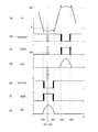
図4(a)〜(e)は、第1実施形態における整流装置132の各部波形を示すグラフ(その1)である。
図5(a)〜(e)は、第1実施形態における整流装置132の各部波形を示すグラフ(その2)である。
図4(a)〜(e)と図5(a)〜(e)の各グラフの縦軸と横軸とは、図18(a)〜(e)の各グラフの縦軸と横軸と同様である。
図4(a)〜(e)と図5(a)〜(e)とは、オフのタイミングが早くなり、整流MOSFET101のドレイン電圧Vdがソース電圧Vsを上回る前に、整流MOSFET101をオフにした場合の波形である。
4A to 4E are graphs (No. 1) showing waveforms of respective parts of the
FIGS. 5A to 5E are graphs (No. 2) showing waveforms of respective parts of the
The vertical and horizontal axes of the graphs in FIGS. 4A to 4E and FIGS. 5A to 5E are the vertical and horizontal axes of the graphs in FIGS. 18A to 18E, respectively. It is the same.
4A to 4E and FIGS. 5A to 5E are turned off before the drain voltage Vd of the rectifying
以下、図4(a)〜(e)を参照して、第1実施形態の自律型の同期整流MOSFETを用いた整流装置132の動作と効果を確認する。
時刻t31において、整流装置132が整流動作を開始するとき、判定回路103の非反転入力端子IN+の電圧Vin+が反転入力端子IN−の電圧Vin−を下回る。このとき、図4(a)に示すように、ドレイン・ソース間電圧Vdsが負になる。
図4(b)に示すように、判定回路103の比較信号Vcompは、HレベルからLレベルへと変化する。比較信号Vcompがゲート駆動回路105の中の各CMOSバッファ163,162,161を伝わって、図4(c)に示すように、ゲート電圧Vgsを昇圧する。このとき、最終段のCMOSバッファ161のハイ側P型MOSFET150にドレイン電流Idhが流れて、ゲート電流Igとなる。このゲート電流Igにより、整流MOSFET101のゲート電圧Vgsが昇圧される。
Hereinafter, with reference to FIGS. 4A to 4E, the operation and effect of the
At time t31, when the
As shown in FIG. 4B, the comparison signal Vcomp of the
第1実施形態の整流装置132では、最終段のCMOSバッファ161のハイ側P型MOSFET150と直列に、ハイ側P型MOSFET150が流せる電流よりも小さい電流を流す定電流回路156が接続されており、整流MOSFET101のドレイン電流Idh(ゲート電流Ig)を制限する。そのため、整流MOSFET101のゲート電圧Vgsを昇圧する速度が遅くなり、判定回路103の比較信号Vcompの振動に追随しなくなる。すなわち、出力の応答性を遅くするフィルタ効果により、ゲート電圧Vgsの振動を抑制可能である。更に、整流MOSFET101と内蔵ダイオード102の間での電流の切り替わりも抑制され、図4(a)に示すように、ドレイン・ソース間電圧Vdsの振動も抑制される。整流MOSFET101のゲート電圧Vgsの振動が抑制されると、図4(d)に示すように、ゲート電流Igの振動も抑制され、コンデンサ107の電荷の不要な消費を減らすことができる。
時刻t32において、図4(a)に示すように、ドレイン・ソース間電圧Vdsが0よりも充分に小さくなる。図4(b)に示すように、比較信号VcompがLレベルで安定し、チャタリングが終了する。
In the
At time t32, as shown in FIG. 4A, the drain-source voltage Vds becomes sufficiently smaller than zero. As shown in FIG. 4B, the comparison signal Vcomp is stabilized at the L level, and chattering ends.
時刻t33において、整流装置132が整流動作を終了するとき、整流MOSFET101のオフの判定が早いので、時刻t31〜t32の整流動作を開始するときと同様に、比較信号Vcompが振動してチャタリングが発生する。しかし、出力の応答性を遅くするフィルタ効果により、ゲート電圧Vgsの振動を抑制可能である。その結果、整流MOSFET101のドレイン・ソース間電圧Vdsとゲート電流Igの振動も抑制でき、コンデンサ107の電荷の不要な消費を減らすことができる。
時刻t34において、図4(a)に示すように、ドレイン・ソース間電圧Vdsが0よりも充分に大きくなる。図4(b)に示すように、比較信号VcompがHレベルで安定し、チャタリングが終了する。
When the
At time t34, as shown in FIG. 4A, the drain-source voltage Vds becomes sufficiently larger than zero. As shown in FIG. 4B, the comparison signal Vcomp is stabilized at the H level, and the chattering ends.
続いて、図5(a)〜(e)を参照して、本発明の自律型の同期整流MOSFETの動作と効果を確認する。
時刻t41において、整流装置132が整流動作を開始するとき、図4の場合と同様に判定回路103の非反転入力端子IN+の電圧Vin+が反転入力端子IN−の電圧Vin−を下回る。図5(a)に示すように、ドレイン・ソース間電圧Vdsが負になる。
図5(b)に示すように、判定回路103の比較信号VcompがHレベルからLレベルへと変化する。比較信号Vcompがゲート駆動回路105の中の各CMOSバッファ163,162,161を伝わって、図5(c)に示すように、ゲート電圧Vgsを昇圧する。このときは、最終段のCMOSバッファ161のハイ側P型MOSFET150に流れるドレイン電流Idhが、図5(d)に示すゲート電流Igとなる。このゲート電流Igは、ゲート電圧Vgsを昇圧する。
Subsequently, referring to FIGS. 5A to 5E, the operation and effect of the autonomous synchronous rectification MOSFET of the present invention will be confirmed.
At time t41, when the rectifying
As shown in FIG. 5B, the comparison signal Vcomp of the
最終段のCMOSバッファ161のハイ側P型MOSFET150と直列に接続した定電流回路156の電流が図4の場合よりも小さいと、図5(d)に示すように、ゲート電流Igが更に制限され、ゲート電圧Vgsを昇圧する速度が更に遅くなる。この場合、整流電流が内蔵ダイオード102から整流MOSFET101に切り替わるのが遅くなり、整流MOSFET101に切り替わったときには、より大きな整流電流が流れる。そうすると、切り替わったときの整流MOSFET101のオン電圧は大きくなるので、判定回路103はオフ判定しにくくなり、チャタリングも起きにくくなる。
If the current of the constant
時刻t42〜t43において、整流装置132が整流動作を終了するときの動作は、図4(a)〜(e)に示した時刻t33〜34の動作と同様である。出力の応答性を遅くするフィルタ効果により、図5(c)に示すように、ゲート電圧Vgsの振動がより抑制される。図5(d)に示すように、ゲート電流Igの振動もより抑制される。よって、図5(a)に示すように、ドレイン・ソース間電圧Vdsの振動もより抑制される。
At time t42 to t43, the operation when the
以上、図4および図5を使って説明したように、第1実施形態の整流装置132は、整流動作の開始時および終了時のチャタリングを抑制する効果を有する。その結果、コンデンサ107の電荷の不要な消費を減らすことができ、小容量のコンデンサで動作させることが可能になり、小面積、低コストの整流装置132を実現できる。更に、電圧および電流の振動に起因したノイズの発生を抑制可能である。
As described above with reference to FIGS. 4 and 5, the
オルタネータ140で発電される交流電力の周波数は、低い場合で50Hz、高い場合でも5kHz程度である。オルタネータ140で発電される交流電力の相電圧の変化は非常に遅く、整流MOSFET101をオンした後に整流電流が徐々に増加する。そのため、整流MOSFET101のオンの動作は、過渡的な挙動を示さない。よって、第1実施形態の整流装置132において、整流MOSFET101をオンするタイミングを遅くしても、オン時のスイッチング損失は小さく、整流の損失は小さい。整流MOSFET101をオンするタイミングを遅くすると、整流MOSFET101よりも導通損失が大きい内蔵ダイオード102に電流が流れる期間が長くなるが、その期間は整流開始の直後であり、そのときの整流電流は小さい。よって、内蔵ダイオード102の導通損失が大きくなっても、全体の整流の損失は、ほぼ変わらない。更に、整流電流がピークに達するまでに充分に時間があるので、ゲート電圧Vgsが充分に上がらずに損失を大きくすることもない。すなわち、オルタネータ140に、第1実施形態の自律型の同期整流MOSFETの整流装置132を用いると、大きなデメリット無しに、チャタリング防止の効果を得ることができる。
The frequency of the AC power generated by the alternator 140 is about 50 Hz when it is low and about 5 kHz when it is high. The change in the phase voltage of the AC power generated by the alternator 140 is very slow, and the rectified current gradually increases after the
第1実施形態の整流装置132には、ノイズが印加されたときにハイサイドとロウサイドの整流素子の貫通電流を防止する効果も備える。整流装置132は、整流MOSFET101のドレイン・ソース間電圧Vdsで整流MOSFET101のオン・オフの判定をする。このとき、判定回路103の誤判定により、整流MOSFET101が誤動作することがある。具体的には、整流装置132の正極側主端子THや負極側主端子TLにノイズが印加されると、判定回路103の比較信号Vcompが反転して、整流MOSFET101のオンとオフが切り替わることがある。
The
オン状態の整流MOSFET101に誤作動を起こすノイズが印加された場合、整流MOSFET101が誤作動を起こしてオフ状態になっている期間、整流MOSFET101の内蔵ダイオード102に整流電流が流れるために、整流動作に問題は生じない。これに対し、オフ状態の整流MOSFET101に誤作動を起こすノイズが印加された場合、他のアームの整流MOSFET101がオン状態であったならば、ハイサイドとロウサイドの整流MOSFET101を通して、バッテリ111の正極側端子から負極側端子へと貫通電流が流れてしまう。このように貫通電流が流れると、バッテリ111に充電した電荷が失われて電力損失となるだけでなく、低抵抗のハイサイドとロウサイドの整流MOSFET101に大電流が流れて、整流装置132が破壊されることがある。オルタネータ140の場合、バッテリ111の正極側端子と負極側端子の間に接続された様々な機器がノイズを発生させることがあるため、ノイズ対策は重要である。
When noise that causes malfunction is applied to the
第1実施形態の整流装置132は、整流MOSFET101がオンするときにはゲート電圧Vgsの昇圧に要する時間が長く、整流MOSFET101がオフするときにはゲート電圧Vgsの降圧に要する時間が短い。そのため、オン状態の整流MOSFET101に誤動作を引き起こすノイズが入ると、短時間に整流MOSFET101がオフ状態になり、ノイズが終わると時間を掛けて整流MOSFET101がオン状態に戻る。この整流MOSFET101がオフする期間には、整流MOSFET101の内蔵ダイオード102に整流電流が流れ、整流動作は問題なく行われる。内蔵ダイオード102に電流が流れると、整流MOSFET101に電流が流れているときと比べて発熱が大きくなるが、この発熱が問題とならないように整流MOSFET101のチップや熱抵抗の設計を行う。
In the
一方、オフ状態の整流MOSFET101に誤動作を引き起こすノイズが入ると、判定回路103がオンの判定をするが、整流MOSFET101がオン状態になるのに時間がかかる。整流MOSFET101のゲート電圧Vgsが整流MOSFET101の閾値電圧を越える前にノイズが終わると、判定回路103がオフの判定をし、整流MOSFET101に整流電流が流れることなく整流MOSFET101は短時間にオフ状態に戻る。すなわち、ノイズが加わっている間、整流MOSFET101に整流電流が流れないので、ハイサイドとロウサイドとの間の貫通電流を抑止できる。整流MOSFET101のオンの速度は、想定されるノイズ印加期間が終わるまでに整流MOSFET101のゲート電圧Vgsが整流MOSFET101の閾値電圧を越えないように設定する。
On the other hand, if noise that causes a malfunction occurs in the
第1実施形態の自律型の同期整流MOSFETの整流装置132では、整流MOSFET101がオンするときにゲート電圧Vgsの昇圧に要する時間が長く、整流MOSFET101がオフするときにゲート電圧Vgsの降圧に要する時間が短い。更に、チャタリング中の整流MOSFET101と内蔵ダイオード102の間での電流の切り替わりを抑制し、ノイズ印加時のハイサイドとロウサイドの整流MOSFET101を流れる貫通電流を防止するためには、特に、ロウサイドの整流MOSFET101のゲート電圧Vgsが下がり始めてから閾値電圧Vthに達するまでの時間を長くすることが重要である。同様に、ハイサイドの整流MOSFET101のゲート電圧Vgsが上がり始めてから閾値電圧Vthに達するまでの時間を長くすることが重要である。
In the
整流MOSFET101がオンするときにゲート電圧Vgsの降圧に要する時間を、ゲート電圧Vgsが最大ゲート電圧の90%となってから閾値電圧Vthに達するまでの時間と定義する。整流MOSFET101がオフするときにゲート電圧Vgsの昇圧に要する時間を、ゲート電圧Vgsが最大ゲート電圧の10%となってから閾値電圧Vthに達するまでの時間と定義する。ここでは、整流MOSFET101がオンするときにゲート電圧Vgsの昇圧に要する時間が、整流MOSFET101がオフするときにゲート電圧Vgsの降圧に要する時間よりも長いことが重要である。
The time required to step down the gate voltage Vgs when the rectifying
図6(a)〜(g)は、第1実施形態の整流装置132と、比較例の整流装置132zに流れる貫通電流を示すグラフである。
図6(a)は、U相131uの中点配線(ノードNu)の電圧Vuの波形を示すグラフである。
図6(b)は、ハイサイド側の整流装置132uhの比較信号VcompHの波形を示すグラフである。
図6(c)は、ハイサイド側の整流装置132uhのゲート駆動回路105のゲート電圧VgsHの波形を示すグラフである。ゲート電圧VgsHは、整流MOSFET101uhのソース電圧Vsを基準としている。
図6(d)は、ハイサイド側の整流装置132uhに流れるドレイン電流IdHを示すグラフである。
FIGS. 6A to 6G are graphs showing through currents flowing through the
FIG. 6A is a graph showing the waveform of the voltage Vu of the midpoint wiring (node Nu) of the
FIG. 6B is a graph showing the waveform of the comparison signal VcompH of the rectifier 132uh on the high side.
FIG. 6C is a graph showing a waveform of the gate voltage VgsH of the
FIG. 6D is a graph showing the drain current IdH flowing through the rectifier 132uh on the high side.
図6(e)は、ロウサイド側の整流装置132ulの比較信号VcompLの波形を示すグラフである。
図6(f)は、ロウサイド側の整流装置132ulのゲート駆動回路105のゲート電圧VgsLの波形を示すグラフである。ゲート電圧VgsLは、整流MOSFET101ulのソース電圧Vsを基準としている。
図6(g)は、ロウサイド側の整流装置132ulに流れるドレイン電流IdLを示すグラフである。
V相131vの電圧や電流は、U相131uと位相が120°シフトした同一波形である。W相131wの電圧や電流は、U相131uと位相が240°シフトした同一波形である。
FIG. 6E is a graph showing a waveform of the comparison signal VcompL of the low-side rectifier 132ul.
FIG. 6F is a graph showing the waveform of the gate voltage VgsL of the
FIG. 6G is a graph showing the drain current IdL flowing through the low-side rectifier 132ul.
The voltage and current of the
図1に示したオルタネータ140を適宜参照しつつ、各部の電圧と電流による動作を説明する。
オルタネータ140において、固定子コイル110uv,110vw,110wuの中を回転子コイル109が回転することで発電が行われる。このとき、固定子コイル110uv,110vw,110wuには、交流電力が発生する。
図6(a)に示すように、固定子コイル110uv,110vw,110wuの交流電力により、U相131uの中点配線(ノードNu)の電圧Vuは、周期的に上下する。整流装置132,132zは、貫通電流を防ぐために、整流の方向とは逆の方向に電流を流さないように動作している。
時刻t60において、電圧Vuが0Vよりも低くなると、同期整流の開始時に整流MOSFET101ulをオンに制御する前に、先ず、高抵抗の内蔵ダイオード102ulに電流が流れてオン電圧が大きくなる。オン電圧が大きくなるとロウサイド側の整流装置132ulの整流MOSFET101ulがオンして、同期整流が開始する。すると、低抵抗の整流MOSFET101ulに電流が流れてオン電圧が下がる。オン電圧が下がりすぎると、整流MOSFET101ulをオフする判定基準に達する。整流MOSFET101ulはオフし、同期整流が終了する。これにより、内蔵ダイオード102ulに電流が流れてオン電圧が大きくなり、整流MOSFET101ulがオンして、再び同期整流が開始する。このように整流MOSFET101ulは、電圧Vuが充分に小さくなるまで、オンとオフとを繰り返す。
With reference to the alternator 140 shown in FIG. 1 as appropriate, the operation of each part by voltage and current will be described.
In the alternator 140, the
As shown in FIG. 6A, the voltage Vu of the midpoint wiring (node Nu) of the
At time t60, when the voltage Vu becomes lower than 0V, before the rectifying MOSFET 101ul is controlled to be turned on at the start of synchronous rectification, first, a current flows through the high-resistance built-in diode 102ul and the on-voltage increases. When the ON voltage increases, the rectification MOSFET 101ul of the rectifier 132ul on the low side is turned on and synchronous rectification starts. Then, a current flows through the low-resistance rectifying MOSFET 101ul, and the on-voltage is lowered. If the on-voltage is too low, the criterion for turning off the rectifying MOSFET 101ul is reached. The rectification MOSFET 101ul is turned off, and the synchronous rectification ends. As a result, a current flows through the built-in diode 102ul, the on-voltage increases, the rectification MOSFET 101ul turns on, and synchronous rectification starts again. As described above, the rectification MOSFET 101ul is repeatedly turned on and off until the voltage Vu becomes sufficiently small.
ここで、時刻t61〜t62において、ノイズにより判定回路103が誤動作し、図6(b)に示す比較信号VcompHがLレベルになった場合を考える。図6(c),(d)において、破線は、第1比較例の整流装置132y(図17参照)の動作を示している。それに対して図6(c),(d)の実線は、第1実施形態の整流装置132(図2参照)の動作を示している。
図6(c)に示すように、第1比較例の整流装置132yでは、ノイズが印加されたときに、ゲート電圧VgsHが閾値電圧Vthを超えて貫通電流が流れる虞がある。それに対して、第1実施形態の整流装置132は、ノイズが印加されたときにゲート電圧VgsHは緩やかに上昇し、閾値電圧Vthを超えない。
図6(d)に示すように、第1比較例の整流装置132yでは、ノイズが印加されたときには、ドレイン電流IdHとして、負の大電流である貫通電流が流れやすい。それに対して、第1実施形態の整流装置132は、ノイズが印加されたときでもオフを維持し、貫通電流が流れにくいという効果が得られる。
Here, consider a case where the
As shown in FIG. 6C, in the
As shown in FIG. 6D, in the
時刻t63において、電圧Vuが0Vよりも高くなると、ロウサイド側の整流装置132ulの整流MOSFET101ulがオフして、同期整流が終了する。すると、内蔵ダイオード102ulに電流が流れてオン電圧が大きくなり、整流MOSFET101ulがオンして、再び同期整流が開始する。このように、整流MOSFET101ulは、電圧Vuが充分に大きくなるまで、オンとオフとを繰り返す。
時刻t64〜t65のハイサイドの動作は、時刻t60〜t63のロウサイドの動作と同様である。
When the voltage Vu becomes higher than 0V at time t63, the rectification MOSFET 101ul of the rectifier 132ul on the low side is turned off, and the synchronous rectification ends. Then, a current flows through the built-in diode 102ul to increase the on-voltage, the rectification MOSFET 101ul is turned on, and synchronous rectification starts again. In this way, the rectification MOSFET 101ul is repeatedly turned on and off until the voltage Vu becomes sufficiently large.
The high-side operation from time t64 to t65 is the same as the low-side operation from time t60 to t63.
以下、図7と図8において整流装置132の判定回路103の変形例を記載する。
図7(a),(b)は、第1実施形態における整流装置132の判定回路103の変形例(A),(B)を示す回路図である。
図7(a)に示す判定回路103aの構成を説明する。判定回路103aは、MOSFETで構成されるコンパレータである。判定回路103aは、定電流回路CC1と、PMOS11,12,13,14,15と、NMOS21,22,23とを備えている。判定回路103aの電源電圧端子VCCとグランド端子GNDとの間には電源が供給されて動作する。判定回路103aは、非反転入力端子IN+のの電圧Vin+と反転入力端子IN−の電圧Vin−とを比較して判定するものである。
PMOS11,12,13は、ミラー回路を構成する。すなわち、PMOS11,12,13のドレインは、電源電圧端子VCCに接続される。PMOS11,12,13のゲートとPMOS11のソースは、それぞれ接続されて、定電流回路CC1に接続される。この定電流回路CC1は、PMOS11,12,13のゲートとPMOS11のソースの接続ノードからグランド端子GNDに向けて電流を流すように接続される。
PMOS14,15のドレインは、PMOS12のソースに接続される。PMOS12,14,15のバックゲートは、電源電圧端子VCCに接続される。PMOS14のゲートは、反転入力端子IN−が接続される。PMOS15のゲートは、非反転入力端子IN+が接続される。PMOS14のソースは、NMOS21のソースと、NMOS21,22のゲートに接続される。PMOS15のソースは、NMOS22のソースと、NMOS23のゲートに接続される。NMOS21,22,23のドレインは、グランド端子GNDに接続される。
PMOS13のソースとNMOS23のソースとは、出力端子OUTに接続される。
Hereinafter, modified examples of the
FIGS. 7A and 7B are circuit diagrams showing modified examples (A) and (B) of the
A configuration of the
The
The drains of the
The source of the
図7(a)に示す判定回路103aの動作を説明する。
定電流回路CC1がPMOS11を流れる電流を決定する。PMOS11,12,13が作るミラー回路により、PMOS12,13には、PMOS11とのチャネル幅の比に応じた定電流が流れる。PMOS12に流れる電流は、PMOS15に流れる電流Iin+とPMOS14に流れる電流Iin−とに分流する。
判定回路103aの非反転入力端子IN+の電圧Vin+が反転入力端子IN−の電圧Vin−より低くなると、PMOS12に流れる電流のうち、PMOS15よりもPMOS14に流れる電流が小さくなる。NMOS21に流れる電流も少なくなってオフする。NMOS21と同じゲート電圧が印加されるNMOS22もオフし、NMOS23のゲート電圧が上がってNMOS23がオンする。その結果、電流Ioff_outが出力端子OUTからグランド端子GNDに流れて、出力端子OUTには、グランド端子GNDに印加されるLレベルの電圧が出力される。
判定回路103aの非反転入力端子IN+の電圧Vin+が反転入力端子IN−の電圧Vin−より高くなると、PMOS12から流れ込む電流のうち、PMOS15よりもPMOS14に流れる電流が大きくなる。PMOS14に流れた電流がNMOS21に流れてオンする。NMOS21と同じゲート電圧が印加されるNMOS22もオンし、NMOS23のゲート電圧が下がってNMOS23がオフする。その結果、電流Ion_outが電源電圧端子VCCから出力端子OUTに流れて、出力端子OUTには、電源電圧端子VCCに印加されるHレベルの電圧が出力される。
The operation of the
The constant current circuit CC1 determines the current flowing through the
When the voltage Vin + at the non-inverting input terminal IN + of the
When the voltage Vin + of the non-inverting input terminal IN + of the
次に、図7(a)に示す判定回路103aの特徴を説明する。
オルタネータ140の場合、バッテリ111の電圧が変動し、それに伴って判定回路103aの電源となるコンデンサ107の電圧が変動してしまう。図7(a)に示すように、判定回路103aを定電流回路CC1で動作させることで、バッテリ111の電圧が変動してコンデンサ107の電圧が変動しても、判定回路103aの動作は影響を受けない。定電流回路CC1には、例えば、ゲートをソースにショートさせたN型デプレッションMOSFETを用いる。定電流回路CC1をN型デプレッションMOSFETからなるシンプルな構成とすることで、判定回路103aの面積を小さくできる。その結果、実装面積が低減され、整流装置132のコストも低減される。定電流回路CC1は、電流の温度依存を小さくする。N型デプレッションMOSFETからなる定電流回路CC1の場合、定電流回路CC1の電流の温度依存が小さくなる閾値電圧を持ったN型デプレッションMOSFETを好適に用いることができる。オルタネータ140の場合、発熱に耐えるように整流素子は高温でも動作する必要があり、温度依存が小さい定電流回路CC1を用いることで、オルタネータ140に用いる場合に必要な広い温度範囲で、判定回路103が同じ判定動作をするように構成できる。定電流回路CC1の電流値は、ノイズ耐性に問題がない範囲で小さくする。これにより、コンデンサ107の容量を小さくでき、実装面積を低減でき、整流装置132のコストも低減できる。
Next, features of the
In the case of the alternator 140, the voltage of the
判定回路103aは、バイポーラトランジスタではなく、MOSFETから成る回路とすることで、コンパレータの消費電流を小さくでき、その結果、コンデンサ107の容量を小さく、実装面積も小さく、整流装置132のコストも小さくすることが可能である。
The
図7(b)に示す判定回路103bの構成を説明する。
判定回路103bは、定電流回路CC2〜CC4と、N型バイポーラトランジスタTR1,TR2と、ダイオードD1,D2とを含んで構成される差動増幅回路であり、整流MOSFET101のオンとオフの判定を行うものである。
定電流回路CC2は、電源電圧端子VCCからN型バイポーラトランジスタTR1のコレクタに向けて接続される。定電流回路CC3は、電源電圧端子VCCからN型バイポーラトランジスタTR1のベースおよびN型バイポーラトランジスタTR2のベースの接続ノードに向けて接続される。
定電流回路CC4は、電源電圧端子VCCからN型バイポーラトランジスタTR2のコレクタに向けて接続される。N型バイポーラトランジスタTR2のコレクタは、出力端子OUTに接続される。定電流回路CC2〜CC4は、この判定回路103bに流れる電流を決定する。
ダイオードD1は、N型バイポーラトランジスタTR1のエミッタから非反転入力端子IN+に向けて接続される。ダイオードD2は、N型バイポーラトランジスタTR2のエミッタから反転入力端子IN−およびグランド端子GNDに向けて接続される。
A configuration of the
The
The constant current circuit CC2 is connected from the power supply voltage terminal VCC toward the collector of the N-type bipolar transistor TR1. The constant current circuit CC3 is connected from the power supply voltage terminal VCC toward the connection node of the base of the N-type bipolar transistor TR1 and the base of the N-type bipolar transistor TR2.
The constant current circuit CC4 is connected from the power supply voltage terminal VCC toward the collector of the N-type bipolar transistor TR2. The collector of the N-type bipolar transistor TR2 is connected to the output terminal OUT. The constant current circuits CC2 to CC4 determine the current flowing through the
The diode D1 is connected from the emitter of the N-type bipolar transistor TR1 toward the non-inverting input terminal IN +. The diode D2 is connected from the emitter of the N-type bipolar transistor TR2 toward the inverting input terminal IN− and the ground terminal GND.
図7(b)に示す判定回路103bの動作を説明する。
判定回路103bの非反転入力端子IN+の電圧Vin+が反転入力端子IN−の電圧Vin−より低くなると、定電流回路CC3を流れる電流がN型バイポーラトランジスタTR1のベースに流れ、N型バイポーラトランジスタTR2のベースには流れなくなる。その結果、N型バイポーラトランジスタTR1がオンに、N型バイポーラトランジスタTR2がオフ状態になり、出力端子OUTには電源電圧端子VCCに印加されているHレベルの電圧が出力される。定電流回路CC2を流れる電流は、N型バイポーラトランジスタTR1のコレクタからエミッタへ流れ、ダイオードD1を通って非反転入力端子IN+へと抜ける。定電流回路CC4を流れる電流は、出力端子OUTへと抜ける。
逆に、判定回路103の非反転入力端子IN+の電圧Vin+が反転入力端子IN−の電圧Vin−より高くなると、定電流回路CC3を流れる電流がN型バイポーラトランジスタTR2のベースに流れ、N型バイポーラトランジスタTR1のベースには流れなくなる。その結果、N型バイポーラトランジスタTR1がオフに、N型バイポーラトランジスタTR2がオン状態になり、出力端子OUTにはグランド端子GNDのLレベルの電圧が出力される。定電流回路CC2には電流が流れなくなり、定電流回路CC4を流れる電流は、N型バイポーラトランジスタTR2のコレクタからエミッタへ流れ、ダイオードD2を通って反転入力端子IN−へと抜ける。
The operation of the
When the voltage Vin + of the non-inverting input terminal IN + of the
Conversely, when the voltage Vin + of the non-inverting input terminal IN + of the
図7(b)に示す判定回路103bの特徴を説明する。
判定回路103bは、電流が流れる経路を変えることで、オン・オフの判定を行うので、ノイズによる誤動作を起こしにくい。また、判定回路103bは、電源電圧端子VCCから非反転入力端子IN+へと電流が流れる経路と、電源電圧端子VCCから反転入力端子IN−へと電流が流れる経路を対称とすることで、各経路の素子の温度依存を打ち消して、回路全体の温度依存を小さくすることが可能である。
判定回路103bは更に、定電流回路CC2〜CC4を用いることで、バッテリ111の電圧が変動しコンデンサ107の電圧が変動しても、その影響を受けない。つまり、判定回路103bは、バッテリ電圧への依存性を小さくすることが可能である。定電流回路CC2〜CC4には、例えば、図7(a)の定電流回路CC1と同様に、ゲートをソースにショートさせたN型デプレッションMOSFETを用いる。
ただし、図7(b)の判定回路103bは、図7(a)のコンパレータのようにMOSFETではなく、N型バイポーラトランジスタTR1,TR2を用いている。N型バイポーラトランジスタTR1,TR2の駆動には、所定の電流が必要であり、消費電流が多くなる虞がある。
A feature of the
Since the
Further, the
However, the
図8(c),(d)は、第1実施形態における整流装置132の判定回路103の変形例(C),(D)を示す回路図である。
図8(c)に示す判定回路103cの構成を説明する。図8(c)に示す回路は、1個のN型バイポーラトランジスタTR3を用いた判定回路103cである。
判定回路103cは、定電流回路CC5,CC6と、N型バイポーラトランジスタTR3と、ダイオードD2,D3とを含んで構成される回路であり、整流MOSFET101のオンとオフの判定を行うものである。
定電流回路CC5は、電源電圧端子VCCからN型バイポーラトランジスタTR3のベースBおよびダイオードD3のアノードAの接続ノードに向けて接続される。
定電流回路CC6は、電源電圧端子VCCからN型バイポーラトランジスタTR3のコレクタCに向けて接続される。N型バイポーラトランジスタTR3のコレクタCは、出力端子OUTに接続される。定電流回路CC5,CC6は、この判定回路103cに流れる電流を決定する。
ダイオードD3は、N型バイポーラトランジスタTR3のベースBから非反転入力端子IN+に向けて接続される。ダイオードD2は、N型バイポーラトランジスタTR2のエミッタEから反転入力端子IN−およびグランド端子GNDに向けて接続される。
FIGS. 8C and 8D are circuit diagrams showing modifications (C) and (D) of the
A configuration of the
The
The constant current circuit CC5 is connected from the power supply voltage terminal VCC toward the connection node of the base B of the N-type bipolar transistor TR3 and the anode A of the diode D3.
The constant current circuit CC6 is connected from the power supply voltage terminal VCC toward the collector C of the N-type bipolar transistor TR3. The collector C of the N-type bipolar transistor TR3 is connected to the output terminal OUT. The constant current circuits CC5 and CC6 determine the current flowing through the
The diode D3 is connected from the base B of the N-type bipolar transistor TR3 toward the non-inverting input terminal IN +. The diode D2 is connected from the emitter E of the N-type bipolar transistor TR2 toward the inverting input terminal IN− and the ground terminal GND.
図8(c)に示す判定回路103cの動作を説明する。
判定回路103cの非反転入力端子IN+の電圧Vin+が反転入力端子IN−の電圧Vin−より低くなると、定電流回路CC5を流れる電流が、N型バイポーラトランジスタTR3のベースBには流れなくなり、順方向電流としてダイオードD3を通って非反転入力端子IN+へ流れる。その結果、N型バイポーラトランジスタTR3がオフ状態になり、出力端子OUTには電源電圧端子VCCに印加されているHレベルの電圧が出力される。定電流回路CC6を流れる電流は、出力端子OUTへ流れる。図2の整流装置132において、整流MOSFET101は、ゲートにLレベルの電圧が印加されるので、オフ状態(第1状態)となる、
逆に、判定回路103cの非反転入力端子IN+の電圧Vin+が反転入力端子IN−の電圧Vin−よりも高くなると、定電流回路CC5を流れる電流がN型バイポーラトランジスタTR3のベースBに流れ、ダイオードD3には流れなくなる。その結果、N型バイポーラトランジスタTR3がオン状態になり、出力端子OUTにはグランド端子GNDのLレベルの電圧が出力される。定電流回路CC5を流れる電流は、N型バイポーラトランジスタTR3のコレクタCからエミッタEへ流れ、順方向電流としてダイオードD3を通って反転入力端子IN−へ流れる。図2の整流装置132において、整流MOSFET101は、ゲートにHレベルの電圧が印加されるので、オン状態(第2状態)となる、
なお、判定回路103cの非反転入力端子IN+と反転入力端子IN−とが、図2とは逆に接続されている場合、第1状態と第2状態とは、オンとオフとが逆になる。
The operation of the
When the voltage Vin + of the non-inverting input terminal IN + of the
Conversely, when the voltage Vin + of the non-inverting input terminal IN + of the
Note that when the non-inverting input terminal IN + and the inverting input terminal IN− of the
図8(c)に示す判定回路103cの特徴を説明する。
図8(c)の判定回路103cは、図7(b)の判定回路103bと同様に、電流が流れる経路を変えることでオン・オフの判定を行うので、判定回路103cがノイズによる誤動作を起こしにくい。
電源電圧端子VCCから反転入力端子IN−(グランド端子GND)への第1経路では、N型バイポーラトランジスタTR3のベースBのP型半導体領域からエミッタEの高濃度N型半導体領域へと電流が流れる。電源電圧端子VCCから非反転入力端子IN+への第2経路では、ダイオードD3のアノードAのP型半導体領域からカソードKの高濃度N型半導体領域へと電流が流れる。両経路ともにP型半導体領域から高濃度N型半導体領域へ電流が流れる。これら半導体領域については、図9で詳細に説明する。
判定回路103cは、ダイオードD3とN型バイポーラトランジスタTR3のベースB・エミッタEとを同一に構成する。これにより、第1経路と第2経路の温度依存を同じとすることができる。判定回路103cは、図7(b)の判定回路103bと同様に、第1経路と第2経路を構成する各素子の温度依存が打ち消し合って、動作の温度依存を小さくすることが可能である。
A feature of the
The
In the first path from the power supply voltage terminal VCC to the inverting input terminal IN− (ground terminal GND), a current flows from the P-type semiconductor region of the base B of the N-type bipolar transistor TR3 to the high-concentration N-type semiconductor region of the emitter E. . In the second path from the power supply voltage terminal VCC to the non-inverting input terminal IN +, a current flows from the P-type semiconductor region of the anode A of the diode D3 to the high-concentration N-type semiconductor region of the cathode K. In both paths, current flows from the P-type semiconductor region to the high-concentration N-type semiconductor region. These semiconductor regions will be described in detail with reference to FIG.
The
更に判定回路103cは、定電流回路CC5,CC6を用いることで、バッテリ111の電圧が変動しコンデンサ107の電圧が変動しても、その影響を受けない。判定回路103cは、バッテリ電圧への依存性を小さくすることが可能である。定電流回路CC5,CC6には、図7(a)の定電流回路CC1と同様に、ゲートをソースにショートさせたN型デプレッションMOSFETを用いる。
図8(c)の判定回路103cは、図7(b)の判定回路103bにおける定電流回路CC2を通ってN型バイポーラトランジスタTR1のコレクタからエミッタへ流れる電流の分だけ、消費電流を減らすことができる。その結果、コンデンサ107の容量を小さく、実装面積も小さく、整流装置132のコストも小さくすることが可能である。
Furthermore, by using the constant current circuits CC5 and CC6, the
The
図8(d)に示す判定回路103dの構成を説明する。
図8(d)に示す判定回路103dは、1個のN型MOSFET31を用いている。
判定回路103dは、定電流回路CC7と、N型MOSFET31とを含んで構成される。定電流回路CC7は、電源電圧端子VCCからN型MOSFET31のドレインに向けて接続される。N型MOSFET31のドレインは、出力端子OUTに接続される。N型MOSFET31のゲートは、非反転入力端子IN+に接続される。N型MOSFET31のソースは、反転入力端子IN−およびグランド端子GNDに接続される。
定電流回路CC7は、この判定回路103dに流れる電流を決定する。
A configuration of the
The
The
The constant current circuit CC7 determines the current flowing through the
図8(d)に示す判定回路103dの動作を説明する。
判定回路103dの非反転入力端子IN+の電圧Vin+が、反転入力端子IN−の電圧Vin−にN型MOSFET31の閾値電圧を加えた電圧より低くなると、N型MOSFET31がオフする。N型MOSFET31がオフすると、出力端子OUTには電源電圧端子VCCに印加されているHレベルの電圧が出力される。定電流回路CC7を流れる電流は、出力端子OUTへと流れる。
逆に、判定回路103の非反転入力端子IN+の電圧Vin+が反転入力端子IN−の電圧Vin−にN型MOSFET31の閾値電圧を加えた電圧より高くなると、N型MOSFET31がオンする。N型MOSFET31がオンすると、出力端子OUTにはグランド端子GNDのLレベルの電圧が出力される。定電流回路CC7を流れる電流は、N型MOSFET31を通って反転入力端子IN−へ流れる。
The operation of the
When the voltage Vin + of the non-inverting input terminal IN + of the
Conversely, when the voltage Vin + of the non-inverting input terminal IN + of the
図8(d)に示す判定回路103dの特徴を説明する。
図8(d)の判定回路103dは、N型MOSFET31の1個のみで構成されているので、回路が簡単であり、消費電流も小さい。回路が簡単であるために、制御IC108の面積を小さくでき、実装面積が低減され、整流装置132のコストも低減される。消費電流が小さいので、コンデンサ107の容量を小さくでき、実装面積を低減でき、整流装置132のコストも低減できる。
A feature of the
Since the
図9(a)〜(c)は、第1実施形態における整流装置132の変形例(C)である判定回路103cのレイアウト図である。
図9(a)〜(c)に示す各レイアウトのうち、最も濃いハッチング部分は、高濃度N型シリコン領域41,46である。最も薄いハッチング部分は、N型シリコン領域45である。中程度の濃さのハッチング部分は、P型シリコン領域42,44である。対角線を有する矩形部分は、絶縁層を貫通する電極(導電体)を示している。破線は、不図示絶縁層の上に構成された導電体を示している。
FIGS. 9A to 9C are layout diagrams of a
Among the layouts shown in FIGS. 9A to 9C, the darkest hatched portions are the high-concentration N-
図9(a)は、レイアウトの平面図を示している。
図の左側には、ダイオードD3が形成されている。ダイオードD3のカソードKは、高濃度N型シリコン領域41で囲われている。高濃度N型シリコン領域41は更に、P型シリコン領域42で囲われている。このP型シリコン領域42は更に、ダイオードD3のアノードAを囲っている。ダイオードD3のカソードKは、導電体に覆われて非反転入力端子IN+(不図示)に接続される。
図の右側には、N型バイポーラトランジスタTR3が形成されている。N型バイポーラトランジスタTR3のエミッタEは、高濃度N型シリコン領域43で囲われ、更にP型シリコン領域44で囲われている。このP型シリコン領域44は更に、N型バイポーラトランジスタTR3のベースBを囲っている。N型バイポーラトランジスタTR3のコレクタCは、高濃度N型シリコン領域46で囲われている。この高濃度N型シリコン領域46とP型シリコン領域44とは、N型シリコン領域45に囲われている。ダイオードD3のアノードAとカソードKは、N型バイポーラトランジスタTR3のベースBとエミッタEと対称にレイアウトされ、同一に構成される。
ダイオードD3のアノードAとN型バイポーラトランジスタTR3のベースBとは、導電体に覆われて電気的に接続され、更に定電流回路CC5(不図示)に電気的に接続される。
N型バイポーラトランジスタTR3のコレクタCは、導電体に覆われて、定電流回路CC6および出力端子OUT(不図示)に電気的に接続される。
FIG. 9A shows a plan view of the layout.
On the left side of the figure, a diode D3 is formed. The cathode K of the diode D3 is surrounded by the high-concentration N-
On the right side of the figure, an N-type bipolar transistor TR3 is formed. The emitter E of the N-type bipolar transistor TR3 is surrounded by a high-concentration N-
The anode A of the diode D3 and the base B of the N-type bipolar transistor TR3 are covered with a conductor and electrically connected, and further electrically connected to a constant current circuit CC5 (not shown).
The collector C of the N-type bipolar transistor TR3 is covered with a conductor and is electrically connected to the constant current circuit CC6 and the output terminal OUT (not shown).
図9(b)は、ダイオードD3のB1−B2断面における断面図を示している。
カソードKは、シリコン酸化膜47を貫通する電極であり、高濃度N型シリコン領域41に接触している。この高濃度N型シリコン領域41は、シリコン酸化膜47の下側に形成されている。高濃度N型シリコン領域41の下側には、P型シリコン領域42が形成されている。
ダイオードD3のアノードAは、シリコン酸化膜47を貫通する電極であり、P型シリコン領域42に接触している。
FIG. 9B shows a cross-sectional view of the diode D3 along the B1-B2 cross section.
The cathode K is an electrode that penetrates the
The anode A of the diode D 3 is an electrode that penetrates the
図9(c)は、N型バイポーラトランジスタTR3のC1−C2断面における断面図を示している。
N型バイポーラトランジスタTR3のエミッタEは、シリコン酸化膜47を貫通する電極であり、高濃度N型シリコン領域43に接触している。この高濃度N型シリコン領域43は、シリコン酸化膜47の下側に形成されている。高濃度N型シリコン領域43の下側には、P型シリコン領域44が形成されている。P型シリコン領域44の下側には、N型シリコン領域45が形成されている。
N型バイポーラトランジスタTR3のベースBは、シリコン酸化膜47を貫通する電極であり、P型シリコン領域44に接触している。
N型バイポーラトランジスタTR3のコレクタCは、高濃度N型シリコン領域46に接触している。この高濃度N型シリコン領域46は、シリコン酸化膜47の下側に形成されている。高濃度N型シリコン領域46の下側には、N型シリコン領域45が形成されている。
ダイオードD3のアノードAとカソードKの断面は、N型バイポーラトランジスタTR3のベースBとエミッタEの断面と対称になるように構成される。これにより、各素子の温度依存を打ち消し合って、判定回路103cの動作の温度依存性を小さくすることが可能である。
FIG. 9C shows a cross-sectional view of the N-type bipolar transistor TR3 in the C1-C2 cross section.
The emitter E of the N-type bipolar transistor TR 3 is an electrode that penetrates the
The base B of the N-type bipolar transistor TR 3 is an electrode that penetrates the
The collector C of the N-type bipolar transistor TR3 is in contact with the high-concentration N-
The cross sections of the anode A and the cathode K of the diode D3 are configured to be symmetrical with the cross sections of the base B and the emitter E of the N-type bipolar transistor TR3. Thereby, it is possible to cancel the temperature dependency of each element and to reduce the temperature dependency of the operation of the
図10は、第2実施形態における自律型の同期整流MOSFETの整流装置132aを示す回路図である。
図10に示す第2実施形態の整流装置132aは、図2に示した第1実施形態の整流装置132とは異なる制御IC108aを備えている。第2実施形態の制御IC108aは更に、第1実施形態の制御IC108とは異なるゲート駆動回路105aを備えている。
第2実施形態のゲート駆動回路105aは、第1実施形態のゲート駆動回路105とは異なる最終段のCMOSバッファ161aを備えている。このCMOSバッファ161aは、ハイ側P型MOSFET150と直列、かつ、整流MOSFET101のゲートをオンするときのドレイン電流Idhの経路には、抵抗R1が接続される、抵抗R1は、ハイ側P型MOSFET150のソース側とドレイン側のいずれに接続されてもよい。第2実施形態の抵抗R1は、第1実施形態の定電流回路156に代わって接続される。
整流MOSFET101をオンするとき、ハイ側P型MOSFET150から抵抗R1へとゲート電流Igが流れる。このゲート電流Igは、抵抗R1によって制限される。
整流MOSFET101をオフするとき、整流MOSFET101のゲート電流Igは、ロウ側N型MOSFET151へと流れる。このゲート電流Igは、抵抗R1によって制限されない。
FIG. 10 is a circuit diagram showing a
The
The
When the rectifying
When the
第2実施形態の整流装置132aは、第1実施形態の整流装置132(図2参照)と同様に、整流MOSFET101をオンするときのゲート電流Igを制限してオンの速度を遅くし、整流MOSFET101をオフするときのゲート電流Igは制限せずにオフの速度を速くする。これによりチャタリングを防止し、ノイズ印加時の貫通電流を防止することが可能である。第1実施形態の整流装置132(図2参照)のように、定電流回路156を用いた場合と比べて、より簡単な回路でオン時のゲート電流Igを制限することが可能である。
Similar to the rectifier 132 (see FIG. 2) of the first embodiment, the
図11は、第3実施形態における自律型の同期整流MOSFETの整流装置132bを示す回路図である。
図11に示す第3実施形態の整流装置132bは、図2に示した第1実施形態の整流装置132とは異なる制御IC108bを備えている。第3実施形態の制御IC108bは更に、第1実施形態の制御IC108とは異なるゲート駆動回路105bを備えている。
第3実施形態のゲート駆動回路105bは、最終段のCMOSバッファ161bの出力と整流MOSFET101のゲートとの間に、抵抗R2とダイオード157とを並列に接続している。
整流MOSFET101をオンするとき、ゲート電流Igは、ハイ側P型MOSFET150から抵抗R2を通って整流MOSFET101のゲートへと流れる。このゲート電流Igは、抵抗R2によって制限される。
整流MOSFET101をオフするとき、ゲート電流Igは、ダイオード157を通ってロウ側N型MOSFET151へと逆方向に流れ、抵抗R2によって制限されない。
FIG. 11 is a circuit diagram showing a
A
In the
When the rectifying
When the
第3実施形態の整流装置132bは、第1実施形態の整流装置132(図2参照)と同様に、整流MOSFET101をオンするときのゲート電流Igを制限してオンの速度を遅くし、整流MOSFET101をオフするときのゲート電流Igは制限せずにオフの速度を早くする。これによりチャタリングを防止し、かつ、ノイズ印加時の貫通電流を防止することが可能である。第1実施形態の整流装置132(図2参照)のように定電流回路156を用いた場合と比べて、第3実施形態では、素子のばらつきの影響や温度依存が大きいが、より簡単な回路でオン時のゲート電流Igを制限することが可能である。
Like the rectifier 132 (see FIG. 2) of the first embodiment, the
図12は、第4実施形態における自律型の同期整流MOSFETの整流装置132cを示す回路図である。
図12に示す第4実施形態の整流装置132cは、図2に示した第1実施形態の整流装置132とは異なる制御IC108cを備えている。第4実施形態の制御IC108cは更に、第1実施形態の制御IC108とは異なるゲート駆動回路105cを備えている。
ゲート駆動回路105cは、1段または複数段のCMOSバッファを含んで構成される。ここでは、最終段のCMOSバッファ161cを図示している。
FIG. 12 is a circuit diagram showing a
A
The
最終段のCMOSバッファ161cは、ハイ側P型MOSFET150cとロウ側N型MOSFET151cとが直列接続された回路を含んで構成される。
第4実施形態のハイ側P型MOSFET150cは、第1実施形態のハイ側P型MOSFET150と比較してチャネル幅W_hが小さいか、または、チャネル長L_hが大きい。これにより、整流MOSFET101は、オン時のゲート電流Igを抑えてオンを遅くすることが可能である。一般的にチャネル長L_hは、チップを製造するプロセスで決まるので、チャネル幅W_hを小さくするとよい。
すなわち、最終段のCMOSバッファ161cは、そのハイ側P型MOSFET150cのチャネル幅W_h、チャネル長L_hとし、そのロウ側N型MOSFET151cのチャネル幅W_l、チャネル長L_lとしたときに、以下の式(1)を満たすように、ハイ側P型MOSFET150cのチャネル幅W_hを設計する。

The high-side P-
That is, the
第4実施形態の整流装置132cは、図2に示した第1実施形態の整流装置132と同様に、整流MOSFET101をオン時のゲート電流Igを減らしてオンを遅くする。第4実施形態の整流装置132cは、それに加えて整流MOSFET101をオフ時のゲート電流Igを増やしてオフを速めることができる。これにより更にチャタリングを防止し、ノイズ印加時の貫通電流を防止可能である。
第4実施形態の整流装置132cは、第1実施形態〜第3実施形態と比較すると、定電流回路156や抵抗やダイオードなどが不要であり、より簡単な回路でオン時のゲート電流Igを減らすことができる。
Similarly to the
Compared with the first to third embodiments, the
制御IC108cの中の判定回路103がオン・オフの判定結果を出力してから、整流MOSFET101がオン・オフするまでの時間を十分に短くする、すなわち、ゲート駆動回路105cの入力から出力までの遅延時間を十分に短くすることで、オルタネータ140に求められる広い範囲の温度、動作周波数で動作できる。
ゲート駆動回路105cの遅延時間は、ゲート駆動回路105cを構成するMOSFETの駆動時間で決まり、高温ほど遅延時間が長くなる温度依存を有する。ゲート駆動回路105cの遅延時間が長いと、整流MOSFET101のオン・オフのタイミングが温度で変化する。またゲート駆動回路105cの遅延時間が長いと、動作周波数が変わり周期が変わったときに整流MOSFET101のオン・オフのタイミングが異なり、整流MOSFET101のオン・オフのタイミングが動作周波数が変化する。
しかし、整流MOSFET101がオンするタイミングが温度や動作周波数に依存して変化しても、内蔵ダイオード102に整流電流が流れる期間が変わり、損失が多少変わるだけであり、大きな問題は生じない。
The time from when the
The delay time of the
However, even if the timing at which the rectifying
整流MOSFET101がオンするタイミングが遅くなるほどチャタリングは起こりにくい条件となる。これに対し、整流MOSFET101をオフするタイミングは、遅くなりすぎると大きな逆方向電流が流れてしまい、早くなりすぎると内蔵ダイオード102に大電流が流れて整流MOSFET101のオン電圧が大きくなりすぎて、チャタリングが起こりやすくなる。したがって、整流MOSFET101をオフするタイミングの温度依存、動作周波数依存を小さくすることが重要である。そのためには、整流MOSFET101をオフするときのゲート駆動回路105の遅延を小さくすればよい。
The later the timing when the rectifying
第4実施形態の整流装置132cは、ゲート駆動回路105cの最終段のCMOSバッファ161cを構成するハイ側P型MOSFET150cのチャネル幅W_hを小さくすることで、最終段のCMOSバッファ161cの入力容量が小さくなり、最終段のCMOSバッファ161cの遅延が小さくなって、入力オフ時の遅延が小さくなる。したがって、第4実施形態の整流装置132cは、オルタネータ140で要求される広い範囲の温度、動作周波数での動作に適する。
In the
図13は、第4実施形態におけるゲート駆動回路105cのチャネル長とチャネル幅を示すレイアウト図である。ここでは、最終段のCMOSバッファ161cのレイアウトを図示している。
ゲート駆動回路105cの最終段CMOSバッファ161c(図12参照)を構成するハイ側P型MOSFET150cとロウ側N型MOSFET151cについて、整流MOSFET101がオンするときに駆動するMOSFETの電流が、整流MOSFET101がオフするときに駆動する方のMOSFETの電流よりも小さくなるように構成する。
ハイ側P型MOSFET150cは、高濃度P型シリコン領域54上に形成されたポリシリコン配線53aによって、チャネルが形成される。ハイ側P型MOSFET150cのチャネル長L_hは、ロウ側N型MOSFET151cのチャネル長L_lと同一長である。ハイ側P型MOSFET150cのチャネル幅は、4μm幅のチャネルが2本形成されているので、合計8μmである。
ロウ側N型MOSFET151cは、高濃度N型シリコン領域52上に形成されたポリシリコン配線53bによって、チャネルが形成される。高濃度N型シリコン領域52は、P型ウェルシリコン領域51で囲われている。ロウ側N型MOSFET151cのチャネル長L_lは、ハイ側P型MOSFET150cのチャネル長L_hと同一長であり、チャネル幅は、4μmが16本形成されているので、合計64μmである。
FIG. 13 is a layout diagram showing the channel length and channel width of the
Regarding the high-side P-
In the high-side P-
In the low-side N-
すなわち、最終段のハイ側P型MOSFET150cのチャネル幅W_hは8μmであり、ロウ側N型MOSFET151cのチャネル幅W_lは64μmである。
That is, the channel width W_h of the high-side P-
第4実施形態のゲート駆動回路105cは、第1実施形態より最終段のCMOSバッファ161cの入力容量(ゲート容量)がその分小さくなり、オフ時の整流MOSFET101がオフするときのゲート駆動回路105cの遅延は従来より更に小さくできる。これにより整流MOSFET101をオフするタイミングの温度依存、周波数依存を小さくできる。加えて、最終段のハイ側P型MOSFET150cのチャネル幅が小さくなった分、回路面積を小さくできる。第1実施形態の最終段のハイ側P型MOSFET150のチャネル幅は128umである。それに対して、第4実施形態の最終段のハイ側P型MOSFET150のチャネル幅は8umであり、著しく小さくなっている。
The
図13では、n型シリコン基板上に回路を形成する場合のレイアウトを示している。これをSOI(Silicon On Insulator)基板上にSOI基板上に形成する場合、P型MOSFETやN型MOSFETは、シリコン酸化膜に囲まれた別の島に形成する。SOI基板を用いることで、高温でのラッチアップによる誤動作を防止可能である。 FIG. 13 shows a layout when a circuit is formed on an n-type silicon substrate. When this is formed on an SOI (Silicon On Insulator) substrate, the P-type MOSFET and the N-type MOSFET are formed on another island surrounded by a silicon oxide film. By using the SOI substrate, malfunction due to latch-up at high temperature can be prevented.
図14は、第4実施形態の変形例の自律型の同期整流MOSFETの整流装置を示す回路図である。第4実施形態の変形例は、図12に示した第4実施形態における自律型の同期整流MOSFETの整流装置132cにおいて、ゲート駆動回路105を3段のCMOSバッファで構成した場合の回路図である。
図14に示す第4実施形態の整流装置132cは、図3に示した第1実施形態の変形例の整流装置132とは異なる制御IC108cを備えている。第4実施形態の制御IC108cは更に、第1実施形態の制御IC108とは異なるゲート駆動回路105cを備えている。
ゲート駆動回路105cは、最終段のCMOSバッファ161cと、1段手前のCMOSバッファ162cと、2段手前のCMOSバッファ163cとを含んで3段で構成される。
FIG. 14 is a circuit diagram showing a rectifier of an autonomous type synchronous rectification MOSFET according to a modification of the fourth embodiment. The modification of the fourth embodiment is a circuit diagram in the case where the
The
The
ゲート駆動回路105cを複数のCMOSバッファ161c〜163cで構成する場合、1つのCMOSバッファを構成するハイ側P型MOSFETとロウ側N型MOSFETのうち、整流MOSFET101がオンするときに駆動するMOSFETの電流が、整流MOSFET101がオフするときに駆動する方のMOSFETの電流よりも小さくなるように構成するとよい。
最終段のCMOSバッファ161cは、図12と同じ構成であり、前記した式(1)を満たすように、ハイ側P型MOSFET150cのチャネル幅W_hを設計する。
When the
The final
最終段から1段手前前のCMOSバッファ162cは、ハイ側P型MOSFET152cとロウ側N型MOSFET153cとが直列接続された回路を含んで構成される。
図14に示す第4実施形態のロウ側N型MOSFET153cは、図3に示した第1実施形態のロウ側N型MOSFET153と比較してチャネル幅W_l2が小さいか、または、チャネル長L_l2が大きい。これにより、整流MOSFET101は、オン時に最終段から1段手前前のCMOSバッファ162cの出力を遅延させ、整流MOSFET101のオンを遅くすることできる。一般的にチャネル長L_l2は、チップを製造するプロセスで決まるので、チャネル幅W_l2を小さくするとよい。
すなわち、最終段の1段手前のCMOSバッファ162cは、そのハイ側P型MOSFET152cをチャネル幅W_h2、チャネル長L_h2とし、そのロウ側N型MOSFET153cをチャネル幅W_l2、チャネル長L_l2としたときに、以下の式(2)を満たすように、チャネル幅W_l2を設計する。
The row-side N-
That is, the
最終段から2段手前前のCMOSバッファ163cは、ハイ側P型MOSFET154cとロウ側N型MOSFET155cとが直列接続された回路を含んで構成される。
図14に示す第4実施形態の変形例のハイ側P型MOSFET154cは、図3に示した第1実施形態のハイ側P型MOSFET154と比較してチャネル幅W_h3が小さいか、または、チャネル長L_h3が大きい。これにより、整流MOSFET101は、オン時に最終段から2段手前前のCMOSバッファ163cの出力を遅延させ、整流MOSFET101のオンを遅くすることできる。一般的にチャネル長L_h3は、チップを製造するプロセスで決まるので、チャネル幅W_h3を小さくするとよい。
最終段の2段手前のCMOSバッファ163cは、そのハイ側P型MOSFET154cをチャネル幅W_h3、チャネル長L_h3とし、そのロウ側N型MOSFET155cをチャネル幅W_l3、チャネル長L_l3としたときに、以下の式(3)を満たすように、チャネル幅W_h3,W_l3を設計する。
The high-side P-
The
図14に示した第4実施形態の変形例の整流装置132cは、図12に示した第4実施形態の整流装置132と同様の効果が得られ、加えて、図15で説明する効果も得ることができる。
The
図15は、第4実施形態の変形例におけるゲート駆動回路105cのチャネル長とチャネル幅を示すレイアウト図である。
ゲート駆動回路105cを複数のCMOSバッファ161c〜163c(図14参照)で構成する場合、1つのCMOSバッファを構成するハイ側P型MOSFETとロウ側N型MOSFETのうち、整流MOSFET101がオンするときに駆動するMOSFETの電流が、整流MOSFET101がオフするときに駆動する方のMOSFETの電流よりも小さくなるように構成する。
ハイ側P型MOSFET150cは、高濃度P型シリコン領域54上に形成されたポリシリコン配線53aによって、チャネルが形成される。ハイ側P型MOSFET150cのチャネル長L_hは、他のチャネル長と同一長であり、チャネル幅は、4μmが2本形成されているので、合計8μmである。
ロウ側N型MOSFET151cは、高濃度N型シリコン領域52上に形成されたポリシリコン配線53bによって、チャネルが形成される。高濃度N型シリコン領域52は、P型ウェルシリコン領域51で囲われている。ロウ側N型MOSFET151cのチャネル長L_lは、他のチャネル長と同一長であり、チャネル幅は、4μm幅のチャネルが16本形成されているので、合計64μmである。図15では、そのうち9本のチャネルを示し、他を省略している。
FIG. 15 is a layout diagram showing the channel length and channel width of the
When the
In the high-side P-
In the low-side N-
すなわち、最終段のハイ側P型MOSFET150cのチャネル幅W_hは8μmであり、ロウ側N型MOSFET151cのチャネル幅W_lは64μmである。
最終段の1段手前のハイ側P型MOSFET152cのチャネル幅W_h2は32μmであり、4μmのチャネルが8本形成されている。図15では、そのうち4本のチャネルを示し、他を省略している。ロウ側N型MOSFET153cのチャネル幅W_l2は2μmである。
最終段の2段手前のハイ側P型MOSFET154cのチャネル幅W_h3は2μmであり、ロウ側N型MOSFET155cのチャネル幅W_l3は4μmである。
最終段の1段手前のロウ側N型MOSFET153cのチャネル幅W_l2を小さくすることで最終段の1段手前のCMOSバッファ162cのゲート容量と2段手前のCMOSバッファ163cのゲート容量を小さくすることが可能である。最終段の2段手前のハイ側P型MOSFET154cのチャネル幅W_h3を小さくすることで、最終段の1段手前CMOSバッファ162cのゲート容量と2段手前のCMOSバッファ163cのゲート容量を小さくすることが可能である。
That is, the channel width W_h of the high-side P-
The channel width W_h2 of the high-side P-
The channel width W_h3 of the high-side P-
By reducing the channel width W_l2 of the low-side N-
図15に示す第4実施形態の変形例のゲート駆動回路105cは、最終段の1段手前のロウ側N型MOSFET153cのチャネル幅W_l2および最終段の2段手前のハイ側P型MOSFET154cのチャネル幅W_h3を小さくすることで、オフ時の整流MOSFET101がオフするときのゲート駆動回路105cの遅延は、最終段の1段手前のロウ側N型MOSFET153cのチャネル幅W_l2および最終段の2段手前のハイ側P型MOSFET154cのチャネル幅W_h3を小さくしなかった場合と比べ、更に小さくできる。これにより整流MOSFET101をオフするタイミングの温度依存、周波数依存を小さくできる。加えて、各チャネル幅が小さくなった分、回路面積を小さくできる。
第1実施形態の変形例の最終段のハイ側P型MOSFET150のチャネル幅は128umである。それに対して、第4実施形態の最終段のハイ側P型MOSFET150のチャネル幅は8umであり、著しく小さくなっている。第1実施形態の変形例の最終段の1段手前のロウ側N型MOSFET153のチャネル幅は16umである。それに対して、第4実施形態の最終段の1段手前のロウ側N型MOSFET153のチャネル幅は2umであり、著しく小さくなっている。第1実施形態の変形例の最終段の2段手前のハイ側P型MOSFET154のチャネル幅は8umである。それに対して、第4実施形態の最終段の1段手前のハイ側P型MOSFET154cのチャネル幅は2umであり、著しく小さくなっている。
第4実施形態のゲート駆動回路105cは更に、チャネル幅が小さいMOSFETと、チャネル幅が大きいMOSFETとが上下(PMOSとNMOS)に互い違いにレイアウトされている。これにより、詰めあって更に回路面積を小さくし、実装面積とコストを低減できる。
加えて、出力の応答性を遅くするフィルタ効果により、最終段の1段手前のCMOSバッファ162および2段手前のCMOSバッファ163の振動を抑制することが可能となる。
The
The channel width of the high-side P-
In the
In addition, it is possible to suppress the vibration of the
図14および図15では、ゲート駆動回路105cを構成する3段のCMOSバッファにおいて、1つのCMOSバッファを構成するハイ側P型MOSFETとロウ側N型MOSFETのうち、整流MOSFET101がオンするときに駆動するMOSFETの電流が、整流MOSFET101がオフするときに駆動する方のMOSFETの電流よりも小さくする構成を説明した。しかし、ゲート駆動回路を構成するCMOSバッファの段数は3段に限らず、他の段数のCMOSバッファで構成しても、同様の効果を得ることができる。
14 and 15, when the
図14および図15に示した複数段のCMOSバッファ161c〜163cで構成されるゲート駆動回路105cは、第1〜第3実施形態にも適用することができ、同様の効果を得ることができる。
The
以上説明したように、本発明の自律型の同期整流MOSFETは、コンデンサ107の容量が大きくせず、複雑な回路を用いずにチャタリング防止の効果を得ることができ、合わせて、ノイズ印加時のハイサイドとロウサイドの整流素子の貫通電流も防止可能である。
As described above, the autonomous synchronous rectification MOSFET of the present invention does not increase the capacitance of the
以上、第1実施形態から第4実施形態の整流装置132をオルタネータ140の整流回路130に用いる場合を示したが、オルタネータ140以外の整流回路130に用いることもできる。
図16は、自律型の整流装置132を用いた電力変換装置141の概略構成を示す回路図である。
図16は、第5実施形態における自律型の整流装置132を用いた電力変換装置141の概略構成を示す回路図である。図1に示す第1実施形態のオルタネータ140と同一の要素には同一の符号を付与している。
電力変換装置141は、交流電源122uv,122vw,122wuと、整流回路130と、平滑コンデンサ123および直流負荷124を備えている。
交流電源122uv,122vw,122wuは、三相交流を供給する電源である。交流電源122uv,122vw,122wuは、Δ接続されている。交流電源122wu,122uvは、整流回路130のノードNuに接続される。交流電源122uv,122vwは、整流回路130のノードNvに接続される。交流電源122vw,122wuは、整流回路130のノードNwに接続される。
As mentioned above, although the case where the
FIG. 16 is a circuit diagram showing a schematic configuration of a
FIG. 16 is a circuit diagram illustrating a schematic configuration of a
The
The AC power supplies 122uv, 122vw, and 122wu are power supplies that supply three-phase AC. The AC power supplies 122uv, 122vw, and 122wu are Δ-connected. AC power supplies 122 wu and 122 uv are connected to node Nu of
整流回路130は、三相交流を直流に整流するブリッジ回路であり、図1に示すオルタネータ140の整流回路130と同様に構成される。整流回路130は、直流端子であるノードNp,Nn間に平滑コンデンサ123(エネルギ蓄積部)および直流負荷124が並列に接続され、直流電力を供給する。
平滑コンデンサ123は、直流電圧を平滑化するコンデンサである。直流負荷124は、直流電力を受けて駆動する任意の負荷であり、例えばモータや照明などである。
The
The smoothing
電力変換装置141においても、各実施形態の整流装置132,132a〜132cを用いることができる。このとき、各整流回路の動作を示す電圧波形と電流波形は、図4(a)〜(e)や図5(a)〜(e)と同一となる。これにより、チャタリングを防止することができ、ノイズ印加時の貫通電流を防止する効果を得ることができる。
Also in the
本発明は上記した実施形態に限定されるものではなく、様々な変形例が含まれる。例えば上記した実施形態は、本発明を分かりやすく説明するために詳細に説明したものであり、必ずしも説明した全ての構成を備えるものに限定されるものではない。ある実施形態の構成の一部を他の実施形態の構成に置き換えることが可能であり、ある実施形態の構成に他の実施形態の構成を加えることも可能である。また、各実施形態の構成の一部について、他の構成の追加・削除・置換をすることも可能である。
各実施形態に於いて、制御線や情報線は、説明上必要と考えられるものを示しており、製品上必ずしも全ての制御線や情報線を示しているとは限らない。実際には、殆ど全ての構成が相互に接続されていると考えてもよい。
The present invention is not limited to the embodiments described above, and includes various modifications. For example, the above-described embodiment has been described in detail for easy understanding of the present invention, and is not necessarily limited to the one having all the configurations described. A part of the configuration of one embodiment can be replaced with the configuration of another embodiment, and the configuration of another embodiment can be added to the configuration of one embodiment. Moreover, it is also possible to add, delete, and replace other configurations for a part of the configuration of each embodiment.
In each embodiment, the control lines and information lines indicate what is considered necessary for the explanation, and not all the control lines and information lines on the product are necessarily shown. Actually, it may be considered that almost all the components are connected to each other.
101 整流MOSFET
102 内蔵ダイオード
103 判定回路
105 ゲート駆動回路
106 ダイオード
107 コンデンサ
108 制御IC
109 回転子コイル
110uv,110vw,110wu 固定子コイル
111 バッテリ
122uv,122vw,122wu 交流電源
123 平滑コンデンサ
124 直流負荷
130 整流回路
132 整流装置
140 オルタネータ
141 電力変換装置
150,150c,152c,154c ハイ側P型MOSFET
151,151c,153c,155c ロウ側N型MOSFET
156 定電流回路
157 ダイオード
161 CMOSバッファ (第1のCMOSバッファ)
162 CMOSバッファ (第2のCMOSバッファ)
163 CMOSバッファ (第3のCMOSバッファ)
164 CMOSインバータ
Idl,Idh ドレイン電流
Vcomp 比較信号
Id ドレイン電流 (整流電流)
Ig ゲート電流
IN+ 非反転入力端子
IN− 反転入力端子
Vds ドレイン・ソース間電圧
Vgs,VgsH,VgsL ゲート電圧
Nu,Nv,Nw ノード (交流端子)
Np,Nn ノード (直流端子)
TH 正極側主端子 (一対の主端子のうち一方)
TL 負極側主端子 (一対の主端子のうち他方)
CC1〜CC7 定電流回路
TR1〜TR3 N型バイポーラトランジスタ
D1〜D3 ダイオード
31 N型MOSFET
OUT 出力端子
GND グランド端子
VCC 電源電圧端子
Vcomp 比較信号
101 Rectifier MOSFET
102 Built-in
109 rotor coil 110uv, 110vw,
151, 151c, 153c, 155c Low-side N-type MOSFET
156 Constant
162 CMOS buffer (second CMOS buffer)
163 CMOS buffer (third CMOS buffer)
164 CMOS inverters Idl, Idh Drain current Vcomp Comparison signal Id Drain current (rectified current)
Ig gate current IN + non-inverting input terminal IN− inverting input terminal Vds drain-source voltage Vgs, VgsH, VgsL gate voltage Nu, Nv, Nw node (AC terminal)
Np, Nn node (DC terminal)
TH Positive side main terminal (One of a pair of main terminals)
TL Negative side main terminal (the other of the pair of main terminals)
CC1 to CC7 Constant current circuits TR1 to TR3 N-type bipolar transistors D1 to D3 Diode 31 N-type MOSFET
OUT Output terminal GND Ground terminal VCC Power supply voltage terminal Vcomp Comparison signal
Claims (7)
前記整流MOSFETの一対の主端子間の電圧を入力し、入力した前記一対の主端子間の電圧に基づいて前記整流MOSFETのオン・オフを判定する判定回路と、
前記判定回路の判定結果により前記整流MOSFETのゲートのオン・オフを行い、前記整流MOSFETをオフするときにゲート電圧の降圧に要する時間よりも前記整流MOSFETをオンするときにゲート電圧の昇圧に要する時間を長くして、前記判定回路の判定結果がチャタリングした際にフイルタ効果によりゲート電圧の振動を抑制するように構成されるゲート駆動回路と、
を備え、
前記ゲート駆動回路は、
ハイ側MOSFETおよびロウ側MOSFETを備えて、出力が前記整流MOSFETのゲートに接続される第1のCMOSバッファと、出力が前記第1のCMOSバッファの入力に接続された第2のCMOSバッファとを含んで構成され、
前記整流MOSFETをオンするときに前記第1のCMOSバッファのハイ側MOSFETに流れる電流は、前記整流MOSFETをオフするときに前記第1のCMOSバッファのロウ側MOSFETに流れる電流よりも小さく、
前記整流MOSFETをオンするときに前記第2のCMOSバッファのロウ側MOSFETに流れる電流は、前記整流MOSFETをオフするときに前記第2のCMOSバッファのハイ側MOSFETに流れる電流よりも小さい、
ことを特徴とする整流装置。 A rectifying MOSFET that performs synchronous rectification;
A determination circuit that inputs a voltage between a pair of main terminals of the rectification MOSFET and determines on / off of the rectification MOSFET based on the input voltage between the pair of main terminals;
The gate of the rectification MOSFET is turned on / off according to the determination result of the determination circuit, and the time required for boosting the gate voltage when turning on the rectification MOSFET is longer than the time required for stepping down the gate voltage when turning off the rectification MOSFET. A gate drive circuit configured to suppress the oscillation of the gate voltage by a filter effect when the time is increased and the determination result of the determination circuit chatters ;
With
The gate driving circuit includes:
A first CMOS buffer including a high-side MOSFET and a low-side MOSFET, the output of which is connected to the gate of the rectifying MOSFET; and the second CMOS buffer of which the output is connected to the input of the first CMOS buffer. Comprising and including
The current that flows through the high-side MOSFET of the first CMOS buffer when the rectifying MOSFET is turned on is smaller than the current that flows through the low-side MOSFET of the first CMOS buffer when the rectifying MOSFET is turned off.
The current that flows through the low-side MOSFET of the second CMOS buffer when the rectifying MOSFET is turned on is smaller than the current that flows through the high-side MOSFET of the second CMOS buffer when the rectifying MOSFET is turned off.
A rectifier characterized by that.
ことを特徴とする請求項1に記載の整流装置。 The second CMOS buffer is configured such that twice the quotient obtained by dividing the gate width of the low-side MOSFET by the gate length is smaller than the quotient obtained by dividing the gate width of the high-side MOSFET by the gate length. ,
The rectifier according to claim 1 .
前記整流MOSFETをオンするときに前記第3のCMOSバッファのハイ側MOSFETに流れる電流は、前記整流MOSFETをオフするときに前記第3のCMOSバッファのロウ側MOSFETに流れる電流よりも小さい、
ことを特徴とする請求項1に記載の整流装置。 The gate drive circuit includes a third CMOS buffer whose output is connected to an input of the second CMOS buffer;
The current that flows through the high-side MOSFET of the third CMOS buffer when the rectifying MOSFET is turned on is smaller than the current that flows through the low-side MOSFET of the third CMOS buffer when the rectifying MOSFET is turned off.
The rectifier according to claim 1 .
ことを特徴とする請求項3に記載の整流装置。 The third CMOS buffer is configured such that twice the quotient obtained by dividing the gate width of the low-side MOSFET by the gate length is larger than the quotient obtained by dividing the gate width of the high-side MOSFET by the gate length. ,
The rectifier according to claim 3 .
前記整流MOSFETの一対の主端子間の電圧を入力し、入力した前記一対の主端子間の電圧に基づいて前記整流MOSFETのオン・オフを判定する判定回路と、
前記判定回路の判定結果により前記整流MOSFETのゲートのオン・オフを行い、前記整流MOSFETをオフするときにゲート電圧の降圧に要する時間よりも前記整流MOSFETをオンするときにゲート電圧の昇圧に要する時間を長くして、前記判定回路の判定結果がチャタリングした際にフイルタ効果によりゲート電圧の振動を抑制するように構成されるゲート駆動回路と、
を備え、
前記ゲート駆動回路は、
ハイ側MOSFETおよびロウ側MOSFETを備えて、出力が前記整流MOSFETのゲートに接続される第1のCMOSバッファを含んで構成され、
前記第1のCMOSバッファは、ハイ側MOSFETのゲート幅をゲート長で除算した商よりも、ロウ側MOSFETのゲート幅をゲート長で除算した商の2倍の方が大きくなるように構成され、
前記整流MOSFETをオンするときに前記第1のCMOSバッファのハイ側MOSFETに流れる電流は、前記整流MOSFETをオフするときに前記第1のCMOSバッファのロウ側MOSFETに流れる電流よりも小さい、
ことを特徴とする整流装置。 A rectifying MOSFET that performs synchronous rectification;
A determination circuit that inputs a voltage between a pair of main terminals of the rectification MOSFET and determines on / off of the rectification MOSFET based on the input voltage between the pair of main terminals;
The gate of the rectification MOSFET is turned on / off according to the determination result of the determination circuit, and the time required for boosting the gate voltage when turning on the rectification MOSFET is longer than the time required for stepping down the gate voltage when turning off the rectification MOSFET. A gate drive circuit configured to suppress the oscillation of the gate voltage by a filter effect when the time is increased and the determination result of the determination circuit chatters ;
With
The gate driving circuit includes:
Comprising a first CMOS buffer comprising a high side MOSFET and a low side MOSFET, the output of which is connected to the gate of the rectifying MOSFET;
The first CMOS buffer is configured such that twice the quotient obtained by dividing the gate width of the low-side MOSFET by the gate length is larger than the quotient obtained by dividing the gate width of the high-side MOSFET by the gate length,
The current that flows through the high-side MOSFET of the first CMOS buffer when the rectifying MOSFET is turned on is smaller than the current that flows through the low-side MOSFET of the first CMOS buffer when the rectifying MOSFET is turned off.
A rectifier characterized by that.
前記整流回路のハイサイドおよびロウサイドにそれぞれ接続される請求項1ないし請求項5のいずれか1項に記載の整流装置と、
を備えることを特徴とするオルタネータ。 A bridge-type rectifier circuit in which the DC terminal is connected to the battery and the AC terminal is connected to the AC power supply;
The rectifier according to any one of claims 1 to 5 , wherein the rectifier is connected to a high side and a low side of the rectifier circuit, respectively.
An alternator characterized by comprising:
前記整流回路のハイサイドおよびロウサイドにそれぞれ接続される請求項1ないし請求項5のいずれか1項に記載の整流装置と、
を備えることを特徴とする電力変換装置。 A bridge-type rectifier circuit in which a DC terminal is connected to the energy storage unit, and an AC terminal is connected to an AC power supply;
The rectifier according to any one of claims 1 to 5 , wherein the rectifier is connected to a high side and a low side of the rectifier circuit, respectively.
A power conversion device comprising:
Priority Applications (6)
| Application Number | Priority Date | Filing Date | Title |
|---|---|---|---|
| JP2013257733A JP6371053B2 (en) | 2013-12-13 | 2013-12-13 | Rectifier, alternator and power converter |
| TW103142188A TWI583118B (en) | 2013-12-13 | 2014-12-04 | Rectifier, alternator and power conversion device |
| EP14870115.4A EP3082244B1 (en) | 2013-12-13 | 2014-12-12 | Rectification device, alternator, and power conversion device |
| CN201480067727.XA CN105814786B (en) | 2013-12-13 | 2014-12-12 | Fairing, alternating current generator and power inverter |
| PCT/JP2014/083028 WO2015088020A1 (en) | 2013-12-13 | 2014-12-12 | Rectification device, alternator, and power conversion device |
| US15/104,116 US9966871B2 (en) | 2013-12-13 | 2014-12-12 | Rectification device, alternator, and power conversion device |
Applications Claiming Priority (1)
| Application Number | Priority Date | Filing Date | Title |
|---|---|---|---|
| JP2013257733A JP6371053B2 (en) | 2013-12-13 | 2013-12-13 | Rectifier, alternator and power converter |
Publications (3)
| Publication Number | Publication Date |
|---|---|
| JP2015116077A JP2015116077A (en) | 2015-06-22 |
| JP2015116077A5 JP2015116077A5 (en) | 2016-11-10 |
| JP6371053B2 true JP6371053B2 (en) | 2018-08-08 |
Family
ID=53371317
Family Applications (1)
| Application Number | Title | Priority Date | Filing Date |
|---|---|---|---|
| JP2013257733A Active JP6371053B2 (en) | 2013-12-13 | 2013-12-13 | Rectifier, alternator and power converter |
Country Status (6)
| Country | Link |
|---|---|
| US (1) | US9966871B2 (en) |
| EP (1) | EP3082244B1 (en) |
| JP (1) | JP6371053B2 (en) |
| CN (1) | CN105814786B (en) |
| TW (1) | TWI583118B (en) |
| WO (1) | WO2015088020A1 (en) |
Families Citing this family (19)
| Publication number | Priority date | Publication date | Assignee | Title |
|---|---|---|---|---|
| CN104953859B (en) * | 2015-07-06 | 2019-03-22 | 安徽省东科半导体有限公司 | A kind of synchronous diode |
| JP6617002B2 (en) | 2015-10-20 | 2019-12-04 | 株式会社 日立パワーデバイス | Rectifier, alternator and power supply using it |
| TWI563488B (en) * | 2016-02-01 | 2016-12-21 | Sitronix Technology Corp | Gate driving circuit |
| JP6623958B2 (en) * | 2016-07-12 | 2019-12-25 | 株式会社デンソー | Drive circuit of the switch to be driven |
| JP6789780B2 (en) * | 2016-11-28 | 2020-11-25 | 株式会社 日立パワーデバイス | Rectifier and alternator using it |
| US10128736B1 (en) | 2017-06-23 | 2018-11-13 | Infineon Technologies Ag | Rectifier device |
| DE102017126060B4 (en) * | 2017-11-08 | 2019-06-27 | Infineon Technologies Austria Ag | CONTROL UNIT FOR A TRANSISTOR COMPONENT |
| EP3503363A1 (en) * | 2017-12-19 | 2019-06-26 | Koninklijke Philips N.V. | Powering microcontrollers |
| US10333425B1 (en) | 2018-05-03 | 2019-06-25 | Linear Technology Holding Llc | Self-biasing ideal diode circuit |
| CN110707945A (en) * | 2018-07-10 | 2020-01-17 | Oppo广东移动通信有限公司 | Rectifier circuit, wireless charging device, power supply equipment and wireless charging system |
| TWI678876B (en) | 2019-01-08 | 2019-12-01 | 朋程科技股份有限公司 | Alternator and rectifier thereof |
| TWI692194B (en) | 2019-06-27 | 2020-04-21 | 朋程科技股份有限公司 | Alternator and rectifier thereof |
| GB2590057B (en) * | 2019-10-10 | 2022-11-16 | Steifpower Tech Company Limited | A Field-Effect Transistor (FET) based synchronous rectifier for emulating a diode |
| US10840795B1 (en) * | 2019-10-16 | 2020-11-17 | Monolithic Power Systems, Inc. | Power transistor driver with reduced spikes for switching converters |
| JP7148476B2 (en) | 2019-10-25 | 2022-10-05 | 株式会社東芝 | Power switch, power rectifier and power converter |
| JP7296331B2 (en) * | 2020-03-18 | 2023-06-22 | 株式会社 日立パワーデバイス | GATE DRIVE DEVICE AND GATE DRIVE METHOD, POWER SEMICONDUCTOR MODULE, AND POWER CONVERTER |
| TWI766395B (en) * | 2020-10-20 | 2022-06-01 | 朋程科技股份有限公司 | Alternator and rectifier thereof |
| TWI746215B (en) * | 2020-10-20 | 2021-11-11 | 朋程科技股份有限公司 | Alternator and rectifier thereof |
| JP7529946B2 (en) * | 2021-02-17 | 2024-08-07 | ミネベアパワーデバイス株式会社 | Rectifier circuit and method for controlling rectifier circuit |
Family Cites Families (22)
| Publication number | Priority date | Publication date | Assignee | Title |
|---|---|---|---|---|
| JPS55117824A (en) * | 1979-03-01 | 1980-09-10 | Mitsubishi Electric Corp | Device for eliminating chattering |
| US5216299A (en) * | 1992-02-13 | 1993-06-01 | Standard Microsystems Corporation | Low power noise rejecting TTL to CMOS input buffer |
| US5583457A (en) | 1992-04-14 | 1996-12-10 | Hitachi, Ltd. | Semiconductor integrated circuit device having power reduction mechanism |
| JPH09105763A (en) * | 1995-10-11 | 1997-04-22 | Nec Corp | Comparator circuit |
| US5877647A (en) * | 1995-10-16 | 1999-03-02 | Texas Instruments Incorporated | CMOS output buffer with slew rate control |
| SE517685C2 (en) * | 2000-03-24 | 2002-07-02 | Ericsson Telefon Ab L M | Method and apparatus for controlling a synchronous rectifier in a DC converter |
| JP3826279B2 (en) * | 2002-02-20 | 2006-09-27 | 富士電機デバイステクノロジー株式会社 | Comparator circuit |
| JP4668679B2 (en) * | 2005-05-16 | 2011-04-13 | 日立オートモティブシステムズ株式会社 | Rotating electrical machine control device |
| JP4867279B2 (en) * | 2005-10-17 | 2012-02-01 | パナソニック株式会社 | Power converter |
| JP5352964B2 (en) * | 2007-03-29 | 2013-11-27 | 富士通セミコンダクター株式会社 | DC-DC converter, power supply voltage supply method, power supply voltage supply system, and control method for DC-DC converter |
| WO2008155917A1 (en) | 2007-06-19 | 2008-12-24 | Panasonic Corporation | Switching element driving circuit |
| DE102007060219A1 (en) | 2007-12-14 | 2009-06-18 | Robert Bosch Gmbh | Rectifier circuit |
| US8022679B2 (en) * | 2008-04-18 | 2011-09-20 | Linear Technology Corporation | Systems and methods for fast switch turn on approximating ideal diode function |
| JP5216424B2 (en) | 2008-06-06 | 2013-06-19 | 日立オートモティブシステムズ株式会社 | CHARGE GENERATOR FOR VEHICLE AND rectifier for the same |
| US8064227B2 (en) * | 2008-09-08 | 2011-11-22 | GM Global Technology Operations LLC | Rectifying circuit for a multiphase electric machine |
| JP2012147591A (en) | 2011-01-13 | 2012-08-02 | Toyota Central R&D Labs Inc | Drive circuit |
| JP6042091B2 (en) * | 2011-05-13 | 2016-12-14 | ローム株式会社 | Switching regulator control circuit, switching regulator and electronic equipment, switching power supply, television |
| JP5736243B2 (en) * | 2011-06-13 | 2015-06-17 | 本田技研工業株式会社 | Power circuit |
| JP5269218B2 (en) | 2012-01-31 | 2013-08-21 | 株式会社東芝 | Switching power supply and electronic equipment |
| JP2013215039A (en) * | 2012-04-02 | 2013-10-17 | Denso Corp | Power conversion device |
| US20140168829A1 (en) * | 2012-12-18 | 2014-06-19 | Eaton Corporation | Gate Drive Circuits that Control Electromagnetic Interference and Switching Losses and Related Methods |
| KR101502153B1 (en) * | 2013-04-30 | 2015-03-12 | 주식회사 맵스 | Active diode driver |
-
2013
- 2013-12-13 JP JP2013257733A patent/JP6371053B2/en active Active
-
2014
- 2014-12-04 TW TW103142188A patent/TWI583118B/en active
- 2014-12-12 US US15/104,116 patent/US9966871B2/en active Active
- 2014-12-12 EP EP14870115.4A patent/EP3082244B1/en active Active
- 2014-12-12 WO PCT/JP2014/083028 patent/WO2015088020A1/en active Application Filing
- 2014-12-12 CN CN201480067727.XA patent/CN105814786B/en active Active
Also Published As
| Publication number | Publication date |
|---|---|
| EP3082244A1 (en) | 2016-10-19 |
| CN105814786A (en) | 2016-07-27 |
| US20160315553A1 (en) | 2016-10-27 |
| US9966871B2 (en) | 2018-05-08 |
| CN105814786B (en) | 2018-07-03 |
| EP3082244B1 (en) | 2020-07-01 |
| EP3082244A4 (en) | 2017-08-16 |
| TW201541847A (en) | 2015-11-01 |
| TWI583118B (en) | 2017-05-11 |
| JP2015116077A (en) | 2015-06-22 |
| WO2015088020A1 (en) | 2015-06-18 |
Similar Documents
| Publication | Publication Date | Title |
|---|---|---|
| JP6371053B2 (en) | Rectifier, alternator and power converter | |
| US9019000B2 (en) | Driver circuit having a storage device for driving switching device | |
| JP6617002B2 (en) | Rectifier, alternator and power supply using it | |
| US8723564B2 (en) | Driving circuit | |
| JP4456569B2 (en) | Power switching element drive circuit | |
| JP5267616B2 (en) | Drive control device | |
| JP3912417B2 (en) | Driving circuit | |
| JP5945629B2 (en) | Level shift circuit | |
| US9627973B2 (en) | Switching power supply device, and inverter, converter, and solar power controller including same | |
| JP6323834B2 (en) | Synchronous rectifier and alternator using the same | |
| CN108123623B (en) | Rectifier and alternator using the same | |
| JP6090007B2 (en) | Driving circuit | |
| JP2014027345A (en) | Semiconductor element drive circuit | |
| JP2023166269A (en) | Power supply semiconductor device and switched capacitor converter | |
| CN117394844A (en) | Level shift circuit, driving circuit, and half-bridge circuit | |
| JP5534076B2 (en) | Drive control device | |
| JP6155179B2 (en) | Rectifier, alternator and power converter | |
| JP5832845B2 (en) | Semiconductor module and power conversion module | |
| JP5563050B2 (en) | Gate drive circuit and power semiconductor module | |
| KR102577722B1 (en) | Upper arm driving circuit, and control method of upper arm driving circuit | |
| WO2024070208A1 (en) | Element evaluation device | |
| JP2012016124A (en) | Semiconductor circuit and dc-dc converter |
Legal Events
| Date | Code | Title | Description |
|---|---|---|---|
| RD02 | Notification of acceptance of power of attorney |
Free format text: JAPANESE INTERMEDIATE CODE: A7422 Effective date: 20160715 |
|
| A521 | Request for written amendment filed |
Free format text: JAPANESE INTERMEDIATE CODE: A523 Effective date: 20160923 |
|
| A621 | Written request for application examination |
Free format text: JAPANESE INTERMEDIATE CODE: A621 Effective date: 20160923 |
|
| A131 | Notification of reasons for refusal |
Free format text: JAPANESE INTERMEDIATE CODE: A131 Effective date: 20171128 |
|
| A521 | Request for written amendment filed |
Free format text: JAPANESE INTERMEDIATE CODE: A523 Effective date: 20180118 |
|
| TRDD | Decision of grant or rejection written | ||
| A01 | Written decision to grant a patent or to grant a registration (utility model) |
Free format text: JAPANESE INTERMEDIATE CODE: A01 Effective date: 20180703 |
|
| A61 | First payment of annual fees (during grant procedure) |
Free format text: JAPANESE INTERMEDIATE CODE: A61 Effective date: 20180712 |
|
| R150 | Certificate of patent or registration of utility model |
Ref document number: 6371053 Country of ref document: JP Free format text: JAPANESE INTERMEDIATE CODE: R150 |
|
| S111 | Request for change of ownership or part of ownership |
Free format text: JAPANESE INTERMEDIATE CODE: R313117 |
|
| R350 | Written notification of registration of transfer |
Free format text: JAPANESE INTERMEDIATE CODE: R350 |
|
| S533 | Written request for registration of change of name |
Free format text: JAPANESE INTERMEDIATE CODE: R313533 |
|
| R350 | Written notification of registration of transfer |
Free format text: JAPANESE INTERMEDIATE CODE: R350 |