JP6367249B2 - Probe unit - Google Patents

Probe unit Download PDF

Info

Publication number
JP6367249B2
JP6367249B2 JP2015562863A JP2015562863A JP6367249B2 JP 6367249 B2 JP6367249 B2 JP 6367249B2 JP 2015562863 A JP2015562863 A JP 2015562863A JP 2015562863 A JP2015562863 A JP 2015562863A JP 6367249 B2 JP6367249 B2 JP 6367249B2
Authority
JP
Japan
Prior art keywords
probe
contact
holder
plunger
diameter
Prior art date
Legal status (The legal status is an assumption and is not a legal conclusion. Google has not performed a legal analysis and makes no representation as to the accuracy of the status listed.)
Active
Application number
JP2015562863A
Other languages
Japanese (ja)
Other versions
JPWO2015122472A1 (en
Inventor
山田 佳男
佳男 山田
浩平 広中
浩平 広中
一也 相馬
一也 相馬
雅宏 高橋
雅宏 高橋
Current Assignee (The listed assignees may be inaccurate. Google has not performed a legal analysis and makes no representation or warranty as to the accuracy of the list.)
NHK Spring Co Ltd
Original Assignee
NHK Spring Co Ltd
Priority date (The priority date is an assumption and is not a legal conclusion. Google has not performed a legal analysis and makes no representation as to the accuracy of the date listed.)
Filing date
Publication date
Application filed by NHK Spring Co Ltd filed Critical NHK Spring Co Ltd
Publication of JPWO2015122472A1 publication Critical patent/JPWO2015122472A1/en
Application granted granted Critical
Publication of JP6367249B2 publication Critical patent/JP6367249B2/en
Active legal-status Critical Current
Anticipated expiration legal-status Critical

Links

Images

Classifications

    • GPHYSICS
    • G01MEASURING; TESTING
    • G01RMEASURING ELECTRIC VARIABLES; MEASURING MAGNETIC VARIABLES
    • G01R1/00Details of instruments or arrangements of the types included in groups G01R5/00 - G01R13/00 and G01R31/00
    • G01R1/02General constructional details
    • G01R1/06Measuring leads; Measuring probes
    • G01R1/067Measuring probes
    • G01R1/06711Probe needles; Cantilever beams; "Bump" contacts; Replaceable probe pins
    • G01R1/06733Geometry aspects
    • G01R1/06738Geometry aspects related to tip portion
    • GPHYSICS
    • G01MEASURING; TESTING
    • G01RMEASURING ELECTRIC VARIABLES; MEASURING MAGNETIC VARIABLES
    • G01R1/00Details of instruments or arrangements of the types included in groups G01R5/00 - G01R13/00 and G01R31/00
    • G01R1/02General constructional details
    • G01R1/04Housings; Supporting members; Arrangements of terminals
    • G01R1/0408Test fixtures or contact fields; Connectors or connecting adaptors; Test clips; Test sockets
    • G01R1/0433Sockets for IC's or transistors
    • G01R1/0441Details
    • G01R1/0466Details concerning contact pieces or mechanical details, e.g. hinges or cams; Shielding
    • GPHYSICS
    • G01MEASURING; TESTING
    • G01RMEASURING ELECTRIC VARIABLES; MEASURING MAGNETIC VARIABLES
    • G01R1/00Details of instruments or arrangements of the types included in groups G01R5/00 - G01R13/00 and G01R31/00
    • G01R1/02General constructional details
    • G01R1/06Measuring leads; Measuring probes
    • G01R1/067Measuring probes
    • G01R1/06711Probe needles; Cantilever beams; "Bump" contacts; Replaceable probe pins
    • G01R1/06716Elastic
    • G01R1/06722Spring-loaded
    • GPHYSICS
    • G01MEASURING; TESTING
    • G01RMEASURING ELECTRIC VARIABLES; MEASURING MAGNETIC VARIABLES
    • G01R1/00Details of instruments or arrangements of the types included in groups G01R5/00 - G01R13/00 and G01R31/00
    • G01R1/02General constructional details
    • G01R1/06Measuring leads; Measuring probes
    • G01R1/067Measuring probes
    • G01R1/073Multiple probes
    • G01R1/07307Multiple probes with individual probe elements, e.g. needles, cantilever beams or bump contacts, fixed in relation to each other, e.g. bed of nails fixture or probe card
    • G01R1/07314Multiple probes with individual probe elements, e.g. needles, cantilever beams or bump contacts, fixed in relation to each other, e.g. bed of nails fixture or probe card the body of the probe being perpendicular to test object, e.g. bed of nails or probe with bump contacts on a rigid support

Description

本発明は、半導体集積回路や液晶パネルなどの検査対象の導通状態検査または動作特性検査に用いられるプローブユニットに関するものである。   The present invention relates to a probe unit used for a conduction state inspection or an operation characteristic inspection of an inspection target such as a semiconductor integrated circuit or a liquid crystal panel.

従来、半導体集積回路や液晶パネルなどの検査対象の導通状態検査や動作特性検査を行う際には、検査対象と検査用信号を出力する信号処理装置との間の電気的な接続を図るために、コンタクトプローブを複数収容するプローブユニットが用いられる。プローブユニットにおいては、近年の半導体集積回路や液晶パネルの高集積化、微細化の進展に伴い、コンタクトプローブ間のピッチを狭小化することにより、高集積化、微細化された検査対象にも適用可能な技術が進歩してきている。   Conventionally, when conducting a conduction state inspection or an operation characteristic inspection of an inspection target such as a semiconductor integrated circuit or a liquid crystal panel, an electrical connection is made between the inspection target and a signal processing device that outputs an inspection signal. A probe unit that accommodates a plurality of contact probes is used. The probe unit can be applied to highly integrated and miniaturized inspection objects by narrowing the pitch between contact probes with the progress of high integration and miniaturization of semiconductor integrated circuits and liquid crystal panels in recent years. Possible technologies are progressing.

半導体集積回路や液晶パネルなどの検査対象の導通状態検査や動作特性検査として、4端子測定法が挙げられる。この4端子測定法を用いるプローブユニットとして、プローブホルダに保持された一組のコンタクトプローブ(プローブ群)によって、各コンタクトプローブの先端を接触対象(被測定体)に接触させて電気特性を測定する技術が開示されている(例えば、特許文献1を参照)。特許文献1で開示されたプローブユニットは、円柱の側面の一部を平面状にカットした先端部を有するコンタクトプローブと、このコンタクトプローブを保持するとともに、先端部と内部壁面とを当接させてコンタクトプローブを位置決めするホルダ孔(保持部)が形成されたプローブホルダと、を備えている。   A four-terminal measurement method can be cited as a conduction state inspection and an operation characteristic inspection for inspection targets such as semiconductor integrated circuits and liquid crystal panels. As a probe unit using this four-terminal measurement method, a pair of contact probes (probe group) held by a probe holder is used to measure the electrical characteristics by bringing the tip of each contact probe into contact with a contact target (object to be measured). A technique is disclosed (for example, see Patent Document 1). The probe unit disclosed in Patent Document 1 includes a contact probe having a tip portion obtained by cutting a part of a side surface of a cylinder into a flat shape, and holding the contact probe and bringing the tip portion and an inner wall surface into contact with each other. And a probe holder in which a holder hole (holding portion) for positioning the contact probe is formed.

特開2012−112709号公報JP 2012-112709 A

しかしながら、特許文献1が開示する技術では、プローブ群におけるコンタクトプローブ間の距離が、コンタクトプローブをそれぞれ保持するホルダ孔の形成間隔や、コンタクトプローブにおける先端部の形成精度に依存する。このため、特許文献1が開示する技術では、ホルダ孔およびコンタクトプローブを高精度に加工する必要が生じる。これに対し、簡易に作製できるとともに、コンタクトプローブの位置決め精度を維持することができる保持部の構成が求められていた。   However, in the technique disclosed in Patent Document 1, the distance between the contact probes in the probe group depends on the formation interval of the holder holes that respectively hold the contact probes and the formation accuracy of the tip portion of the contact probes. For this reason, in the technique disclosed in Patent Document 1, it is necessary to process the holder hole and the contact probe with high accuracy. On the other hand, there has been a demand for a configuration of a holding portion that can be easily manufactured and can maintain the positioning accuracy of the contact probe.

本発明は、上記に鑑みてなされたものであって、プローブ群におけるコンタクトプローブの位置決め精度を維持するとともに、簡易に作製することができるプローブユニットを提供することを目的とする。   The present invention has been made in view of the above, and an object of the present invention is to provide a probe unit that can be easily manufactured while maintaining the positioning accuracy of a contact probe in a probe group.

上述した課題を解決し、目的を達成するために、本発明にかかるプローブユニットは、長手方向の一方の端部側で接触対象の一つの電極とそれぞれ接触する二つのコンタクトプローブからなるプローブ群を複数備えるとともに、前記コンタクトプローブを保持するプローブホルダを備え、各コンタクトプローブが、他方の端部側で基板の異なる電極とそれぞれ接触するプローブユニットであって、前記コンタクトプローブは、柱状をなして延びる基部と、前記基部から延びるとともに、該基部の長手方向に対して傾斜した第1の傾斜面を有する傾斜部と、前記傾斜部の前記基部に連なる側と異なる端部から延び、前記基部の長手方向に平行な平面をなす平面部を有する延在部と、前記延在部の前記傾斜部に連なる側と異なる端部から延びるとともに、前記基部の長手方向に対する傾斜角度が、前記第1の傾斜面の傾斜角度と等しい第2の傾斜面を有し、先端で前記接触対象の一つの電極と接触する接触部と、を有し、前記プローブホルダには、複数の前記コンタクトプローブを保持する複数のホルダ孔と、当該プローブホルダの上端面に開口を有し、前記複数のホルダ孔の一端と連通するとともに、内部壁面で前記平面部を支持して複数の前記コンタクトプローブを該内部壁面に沿って配列させる長孔と、が形成されていることを特徴とする。   In order to solve the above-described problems and achieve the object, a probe unit according to the present invention includes a probe group including two contact probes that respectively contact one electrode to be contacted on one end side in the longitudinal direction. A probe unit including a plurality of probe holders for holding the contact probes, wherein each contact probe is in contact with a different electrode on the substrate on the other end side, and the contact probes extend in a columnar shape. A base part, an inclined part extending from the base part and having a first inclined surface inclined with respect to a longitudinal direction of the base part, and an end part extending from a side different from a side connected to the base part of the inclined part; An extension part having a flat part that forms a plane parallel to the direction, and an extension part that extends from a different end from the side connected to the inclined part. In addition, a contact portion that has a second inclined surface having an inclination angle with respect to the longitudinal direction of the base portion equal to the inclination angle of the first inclined surface, and is in contact with one electrode of the contact target at the tip, The probe holder has a plurality of holder holes for holding the plurality of contact probes, an opening at an upper end surface of the probe holder, communicates with one end of the plurality of holder holes, and has an inner wall surface. An elongated hole for supporting the planar portion and arranging the plurality of contact probes along the inner wall surface is formed.

また、本発明にかかるプローブユニットは、上記の発明において、前記接触部は、前記先端に形成され、それぞれが先細な形状をなす複数の先鋭端を有し、前記複数の先鋭端のうち隣り合う二つの先鋭端の対向する壁面がなす角度は、前記第1の傾斜面の傾斜角度の二倍であることを特徴とする。   In the probe unit according to the present invention as set forth in the invention described above, the contact portion is formed at the tip, and has a plurality of sharp ends each having a tapered shape, and is adjacent to the plurality of sharp ends. The angle formed by the opposing wall surfaces of the two sharp ends is twice the inclination angle of the first inclined surface.

また、本発明にかかるプローブユニットは、上記の発明において、前記長孔は、前記プローブ群の配列方向と平行であって、かつ前記プローブ群を構成する前記コンタクトプローブが互いに対向する方向と直交する方向に延びることを特徴とする。   In the probe unit according to the present invention, in the above invention, the long hole is parallel to the arrangement direction of the probe group, and is orthogonal to the direction in which the contact probes constituting the probe group face each other. It extends in the direction.

また、本発明にかかるプローブユニットは、上記の発明において、前記コンタクトプローブは、前記基部の前記傾斜部に連なる側と異なる端部から延び、前記基部の径と比して大きい径を有するフランジ部を有し、前記フランジ部が前記プローブホルダと当接することで、該プローブホルダに保持されることを特徴とする。   In the probe unit according to the present invention, in the above invention, the contact probe extends from an end different from the side connected to the inclined portion of the base, and has a flange portion having a diameter larger than the diameter of the base. And the flange portion is held by the probe holder by contacting the probe holder.

また、本発明にかかるプローブユニットは、上記の発明において、前記コンタクトプローブは、前記基部、前記傾斜部、前記延在部および前記接触部を有する第1プランジャと、前記基板の電極と接触する第2プランジャと、前記第1および第2プランジャの間に設けられて、該第1および第2プランジャを伸縮自在に連結するコイルばねと、を有し、前記プローブホルダは、前記長孔が形成され、前記第1プランジャを保持する第1部材と、前記第2プランジャおよび前記コイルばねを保持し、前記第1部材を着脱自在な第2部材と、を有することを特徴とする。   In the probe unit according to the present invention, in the above invention, the contact probe includes a first plunger having the base portion, the inclined portion, the extending portion, and the contact portion, and a first plunger in contact with the electrode of the substrate. Two plungers and a coil spring provided between the first and second plungers to connect the first and second plungers in a telescopic manner. The probe holder has the elongated hole formed therein. And a first member that holds the first plunger, and a second member that holds the second plunger and the coil spring and is detachable from the first member.

本発明によれば、コンタクトプローブが、基部と、該基部の長手方向に対して傾斜した第1の傾斜面を有する傾斜部と、基部の長手方向に平行な平面をなす平面部を有する延在部と、基部の長手方向に対する傾斜角度が、第1の傾斜面の傾斜角度と等しい第2の傾斜面を有し、先端で接触対象の一つの電極と接触する接触部と、を有し、プローブホルダには、複数の前記コンタクトプローブを保持する複数のホルダ孔と、プローブホルダの上端面に開口を有し、複数のホルダ孔の一端と連通するとともに、内部壁面で平面部を支持して複数のコンタクトプローブを内部壁面に沿って配列させる長孔と、が形成されるようにしたので、プローブ群におけるコンタクトプローブの位置決め精度を維持するとともに、簡易に作製することができるという効果を奏する。   According to the present invention, the contact probe has a base portion, an inclined portion having a first inclined surface inclined with respect to the longitudinal direction of the base portion, and an extended plane portion forming a plane parallel to the longitudinal direction of the base portion. And a contact portion that has a second inclined surface whose inclination angle with respect to the longitudinal direction of the base portion is equal to the inclination angle of the first inclined surface, and contacts with one electrode to be contacted at the tip, The probe holder has a plurality of holder holes for holding the plurality of contact probes, an opening at the upper end surface of the probe holder, communicates with one end of the plurality of holder holes, and supports a flat portion by an inner wall surface. Since the long holes for arranging the plurality of contact probes along the inner wall surface are formed, the positioning accuracy of the contact probes in the probe group can be maintained and can be easily manufactured. Achieve the cormorant effect.

図1は、本発明の実施の形態1にかかるプローブユニットの構成を示す斜視図である。FIG. 1 is a perspective view showing the configuration of the probe unit according to the first embodiment of the present invention. 図2は、本発明の実施の形態1にかかるプローブユニットの要部の構成を示す部分断面図である。FIG. 2 is a partial cross-sectional view showing a configuration of a main part of the probe unit according to the first embodiment of the present invention. 図3は、本発明の実施の形態1にかかるプローブユニットの要部の構成を示す部分断面図である。FIG. 3 is a partial cross-sectional view illustrating a configuration of a main part of the probe unit according to the first embodiment of the present invention. 図4は、本発明の実施の形態1にかかるプローブユニットの要部の構成を示す図である。FIG. 4 is a diagram illustrating a configuration of a main part of the probe unit according to the first embodiment of the present invention. 図5は、本発明の実施の形態1にかかる半導体集積回路の検査時におけるプローブユニットの要部の構成を示す部分断面図である。FIG. 5 is a partial cross-sectional view showing a configuration of a main part of the probe unit at the time of inspection of the semiconductor integrated circuit according to the first embodiment of the present invention. 図6は、本発明の実施の形態1にかかるプローブユニットのプランジャの製造方法を説明する図である。FIG. 6 is a diagram illustrating a method for manufacturing the plunger of the probe unit according to the first embodiment of the present invention. 図7は、本発明の実施の形態1にかかるプローブユニットのプランジャの製造方法を説明する図である。FIG. 7 is a diagram for explaining a method of manufacturing the plunger of the probe unit according to the first embodiment of the present invention. 図8は、本発明の実施の形態1にかかるプローブユニットのプランジャの製造方法を説明する図である。FIG. 8 is a diagram illustrating a method for manufacturing the plunger of the probe unit according to the first embodiment of the present invention. 図9は、本発明の実施の形態1の変形例にかかるプローブユニットのプランジャの構成を示す図である。FIG. 9 is a diagram illustrating a configuration of the plunger of the probe unit according to the modification of the first embodiment of the present invention. 図10は、本発明の実施の形態2にかかるプローブユニットの要部の構成を示す部分断面図である。FIG. 10 is a partial cross-sectional view showing the configuration of the main part of the probe unit according to the second embodiment of the present invention. 図11は、本発明の実施の形態2の変形例にかかるプローブユニットの要部の構成を示す部分断面図である。FIG. 11 is a partial cross-sectional view illustrating a configuration of a main part of a probe unit according to a modification of the second embodiment of the present invention.

以下、本発明を実施するための形態を図面と共に詳細に説明する。なお、以下の実施の形態により本発明が限定されるものではない。また、以下の説明において参照する各図は、本発明の内容を理解でき得る程度に形状、大きさ、および位置関係を概略的に示してあるに過ぎない。すなわち、本発明は各図で例示された形状、大きさ、および位置関係のみに限定されるものではない。   DESCRIPTION OF EMBODIMENTS Hereinafter, embodiments for implementing the present invention will be described in detail with reference to the drawings. In addition, this invention is not limited by the following embodiment. The drawings referred to in the following description only schematically show the shape, size, and positional relationship so that the contents of the present invention can be understood. That is, the present invention is not limited only to the shape, size, and positional relationship illustrated in each drawing.

(実施の形態1)
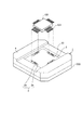
図1は、本発明の実施の形態1にかかるプローブユニットの構成を示す斜視図である。図1に示すプローブユニット1は、検査対象物である半導体集積回路の電気特性検査を行う際に使用する装置であって、半導体集積回路を封入する半導体パッケージ100の接続用電極と半導体集積回路へ検査用信号を出力する回路基板200との間を電気的に接続する装置である。半導体パッケージ100の接続用電極は、図1に示すリード101であって、半導体集積回路に接続されている。
(Embodiment 1)
FIG. 1 is a perspective view showing the configuration of the probe unit according to the first embodiment of the present invention. A probe unit 1 shown in FIG. 1 is an apparatus used when performing an electrical characteristic test on a semiconductor integrated circuit, which is an object to be tested. The probe unit 1 is connected to a connection electrode and a semiconductor integrated circuit of a semiconductor package 100 enclosing the semiconductor integrated circuit. This is an apparatus for electrically connecting the circuit board 200 that outputs a test signal. The connection electrode of the semiconductor package 100 is the lead 101 shown in FIG. 1 and is connected to the semiconductor integrated circuit.

プローブユニット1は、長手方向の一方の端部側で被接触体である半導体パッケージ100の一つの接続用電極(リード101)と接触し、他方の端部側で回路基板200の異なる電極とそれぞれ接触する二つのコンタクトプローブ2a(以下、単に「プローブ2a」という)からなるプローブ群2を複数備えるとともに、複数のプローブ群2を所定のパターンにしたがって収容して保持するプローブホルダ3と、プローブホルダ3の周囲に設けられ、検査の際に複数のプローブ群2と接触する半導体パッケージ100の位置ずれが生じるのを抑制するホルダ部材4と、を有する。   The probe unit 1 is in contact with one connection electrode (lead 101) of the semiconductor package 100, which is a contact object, on one end side in the longitudinal direction, and different electrodes on the circuit board 200 on the other end side. A probe holder 3 that includes a plurality of probe groups 2 including two contact probes 2a (hereinafter simply referred to as “probes 2a”) that are in contact with each other, and that accommodates and holds the plurality of probe groups 2 according to a predetermined pattern; 3, and a holder member 4 that suppresses the occurrence of displacement of the semiconductor package 100 that contacts the plurality of probe groups 2 during inspection.

図2は、プローブホルダ3に収容されるプローブ群2の詳細な構成を示す部分断面図であって、プローブ群2の配列方向に直交する方向の平面を切断面とする断面である。図3は、プローブホルダ3に収容されるプローブ群2の詳細な構成を示す部分断面図であって、プローブ群2の配列方向に平行な平面を切断面とする断面である。図2,3に示すプローブ群2は、導電性材料を用いて形成される二つのプローブ2aが、高さが揃うように並列に配設されてなる。また、各プローブ群2は、プローブ2aの配列方向と直交する方向に配列される。   FIG. 2 is a partial cross-sectional view showing a detailed configuration of the probe group 2 accommodated in the probe holder 3, and is a cross section with a plane in a direction orthogonal to the arrangement direction of the probe group 2 as a cut surface. FIG. 3 is a partial cross-sectional view showing a detailed configuration of the probe group 2 accommodated in the probe holder 3, and is a cross section having a plane parallel to the arrangement direction of the probe group 2 as a cut surface. The probe group 2 shown in FIGS. 2 and 3 is formed by arranging two probes 2a formed using a conductive material in parallel so as to have the same height. Each probe group 2 is arranged in a direction orthogonal to the arrangement direction of the probes 2a.

プローブ2aは、半導体集積回路の検査を行なうときにその半導体パッケージ100のリード101に接触する第1プランジャ21と、検査回路を備えた回路基板200の電極に接触する第2プランジャ22と、第1プランジャ21と第2プランジャ22との間に設けられて二つの第1プランジャ21および第2プランジャ22を伸縮自在に連結するコイルばね23とを備える。プローブ2aを構成する第1プランジャ21および第2プランジャ22、ならびにコイルばね23は同一の軸線を有している。プローブ2aは、半導体パッケージ100をコンタクトさせた際に、コイルばね23が軸線方向に伸縮することによって半導体パッケージ100の接続用電極への衝撃を和らげるとともに、半導体パッケージ100および回路基板200に荷重を加える。   The probe 2a includes a first plunger 21 that contacts the lead 101 of the semiconductor package 100 when inspecting the semiconductor integrated circuit, a second plunger 22 that contacts an electrode of the circuit board 200 provided with the inspection circuit, and a first plunger. A coil spring 23 is provided between the plunger 21 and the second plunger 22 so as to connect the two first plungers 21 and the second plunger 22 in a telescopic manner. The first plunger 21 and the second plunger 22 and the coil spring 23 constituting the probe 2a have the same axis. When the probe 2a is brought into contact with the semiconductor package 100, the coil spring 23 expands and contracts in the axial direction, so that the impact on the connection electrode of the semiconductor package 100 is reduced and a load is applied to the semiconductor package 100 and the circuit board 200. .

第1プランジャ21は、先細な先端形状をなす先端部21aと、先端部21aの基端側から延び、先端部21aの径と比して大きい径を有するフランジ部21bと、フランジ部21bの先端部21aに連なる側と異なる端部から延び、フランジ部21bの径と比して小さい径を有するボス部21cと、ボス部21cのフランジ部21bに連なる側と異なる端部から延び、ボス部21cの径と略同一の径を有する基端部21dとを略同軸上に有する。また、基端部21dは、先端がR面取りされた形状をなす。   The first plunger 21 includes a distal end portion 21a having a tapered distal end shape, a flange portion 21b extending from the proximal end side of the distal end portion 21a and having a diameter larger than the diameter of the distal end portion 21a, and the distal end of the flange portion 21b. The boss 21c extends from an end different from the side connected to the portion 21a and has a smaller diameter than the diameter of the flange 21b, and the boss 21c extends from an end different from the side connected to the flange 21b of the boss 21c. And a base end portion 21d having a diameter substantially the same as the diameter of the first axis. Further, the base end portion 21d has a shape with a chamfered tip.

先端部21aは、フランジ部21bのボス部21cに連なる側と異なる側の端部から略円柱状をなして延びる基部211と、基部211のフランジ部21bに連なる側と異なる端部から延びるとともに、基部211の長手方向を斜めにカットしてなる傾斜面212a(第1の傾斜面)を有する傾斜部212と、傾斜部212の基部211に連なる側と異なる端部から延びる延在部213と、延在部213の傾斜部212に連なる側と異なる端部から延びるとともに、延在部213の長手方向に対して斜めにカットしてなる傾斜面214a(第2の傾斜面)を有し、先端で半導体パッケージ100のリード101と接触する接触部214と、を有する。   The distal end portion 21a extends from an end portion of the flange portion 21b that is substantially cylindrical from an end portion that is different from the side that is continuous with the boss portion 21c, and extends from an end portion that is different from the end portion of the base portion 211 that is continuous to the flange portion 21b. An inclined portion 212 having an inclined surface 212a (first inclined surface) formed by obliquely cutting the longitudinal direction of the base portion 211, an extending portion 213 extending from an end portion different from the side connected to the base portion 211 of the inclined portion 212, and The extending portion 213 has an inclined surface 214a (second inclined surface) that extends from an end different from the side connected to the inclined portion 212 and is obliquely cut with respect to the longitudinal direction of the extending portion 213. And a contact portion 214 that contacts the lead 101 of the semiconductor package 100.

延在部213は、円柱の側面の一部を長手方向に沿って平面状にカットしてなる平面部213aを有し、長手方向と直交する平面を切断面とする断面がD字状をなす。   The extending portion 213 has a flat surface portion 213a formed by cutting a part of the side surface of the cylinder in a planar shape along the longitudinal direction, and a cross section having a plane perpendicular to the longitudinal direction as a cut surface has a D-shape. .

第2プランジャ22は、先細な先端形状を有する先端部22aと、先端部22aの基端側から延び、先端部22aの径と比して大きい径を有するフランジ部22bと、フランジ部22bの先端部22aに連なる側と異なる端部から延び、ボス部21cの径と略同一の径を有するボス部22cと、ボス部22cのフランジ部22bに連なる側と異なる端部から延び、ボス部21c,22cの径と略同一の径を有する基端部22dとを同軸上に有する。この第2プランジャ22は、コイルばね23の伸縮作用によって軸線方向に移動が可能であり、コイルばね23の弾性力によって回路基板200方向に付勢され、回路基板200の電極と接触する。なお、第2接触部は、先端部22aとフランジ部22bとに対応する。   The second plunger 22 has a distal end portion 22a having a tapered distal end shape, a flange portion 22b extending from the proximal end side of the distal end portion 22a and having a diameter larger than the diameter of the distal end portion 22a, and the distal end of the flange portion 22b. The boss portion 22c extends from an end different from the side connected to the portion 22a, has a diameter substantially the same as the diameter of the boss portion 21c, and extends from an end different from the side connected to the flange portion 22b of the boss portion 22c. A base end portion 22d having a diameter substantially the same as the diameter of 22c is coaxially provided. The second plunger 22 can move in the axial direction by the expansion and contraction action of the coil spring 23, is urged toward the circuit board 200 by the elastic force of the coil spring 23, and contacts the electrode of the circuit board 200. The second contact portion corresponds to the tip portion 22a and the flange portion 22b.

コイルばね23は、第1プランジャ21側がボス部21cの径と略同一の内径で巻回された密着巻き部23aである一方、第2プランジャ22側が基端部22dの径以上の内径で所定ピッチに巻回された粗巻き部23bである。密着巻き部23aの端部は、例えばボス部21cと略等しい内径の場合、ボス部21cに圧入されて、フランジ部21bに当接している。一方、粗巻き部23bの端部は、ボス部22cに圧入され、フランジ部22bに当接している。なお、コイルばね23は、密着巻き部23aおよび粗巻き部23bの内径が、同一の内径で巻回されていることが好ましい。このとき、第1プランジャ21および第2プランジャ22とコイルばね23とは、半田付けによって接合されていてもよい。   The coil spring 23 is a tightly wound portion 23a wound on the first plunger 21 side with an inner diameter substantially the same as the diameter of the boss portion 21c, while the second plunger 22 side has an inner diameter equal to or larger than the diameter of the base end portion 22d and a predetermined pitch. It is the rough winding part 23b wound around. For example, when the inner diameter of the tightly wound portion 23a is substantially equal to the boss portion 21c, the end portion is pressed into the boss portion 21c and is in contact with the flange portion 21b. On the other hand, the end of the rough winding portion 23b is press-fitted into the boss portion 22c and is in contact with the flange portion 22b. In addition, as for the coil spring 23, it is preferable that the internal diameter of the close_contact | adherence winding part 23a and the rough winding part 23b is wound by the same internal diameter. At this time, the first plunger 21 and the second plunger 22 and the coil spring 23 may be joined by soldering.

コイルばね23に用いられる線材は、所定荷重が加わったときの粗巻き部23bの縮み量が、初期荷重が加わったとき、例えば、プローブ2aがプローブホルダ3に収容された状態における基端部22dと密着巻き部23aとの最短距離より大きくなるようなばね特性(ストローク)を有する導電性の金属が用いられる。このばね特性を有するコイルばね23を用いることによって、プローブ2aに所定荷重を加えた場合に基端部22dを密着巻き部23a内に摺接させ、基端部22dと密着巻き部23aとの間の電気的導通が可能となる。   The wire rod used for the coil spring 23 has a base end portion 22d in a state in which the probe 2a is accommodated in the probe holder 3, for example, when the amount of contraction of the rough winding portion 23b when a predetermined load is applied is applied. A conductive metal having a spring characteristic (stroke) that is larger than the shortest distance between the contact winding portion 23a and the contact winding portion 23a is used. By using the coil spring 23 having this spring characteristic, when a predetermined load is applied to the probe 2a, the base end portion 22d is brought into sliding contact with the tightly wound portion 23a, and the proximal end portion 22d and the tightly wound portion 23a are in contact with each other. Can be electrically connected.

プローブホルダ3は、樹脂、マシナブルセラミック、シリコンなどの絶縁性材料を用いて形成され、図2の上面側に位置する第1部材31と下面側に位置する第2部材32とが積層されてなる。第1部材31および第2部材32には、複数のプローブ2aを収容するための長孔33、ホルダ孔34およびホルダ孔35からなる保持部が形成されている。長孔33、ホルダ孔34およびホルダ孔35の形成位置は、半導体パッケージ100の配線パターンに応じて定められる。   The probe holder 3 is formed using an insulating material such as resin, machinable ceramic, silicon, etc., and a first member 31 located on the upper surface side and a second member 32 located on the lower surface side in FIG. 2 are laminated. Become. The first member 31 and the second member 32 are formed with a holding portion including a long hole 33, a holder hole 34, and a holder hole 35 for accommodating a plurality of probes 2a. The formation positions of the long hole 33, the holder hole 34, and the holder hole 35 are determined according to the wiring pattern of the semiconductor package 100.

図4は、本実施の形態1にかかるプローブユニットの要部の構成を示す図である。長孔33は、プローブホルダ3の上端面に開口を有し、プローブ群2の配設方向に沿って延びている。また、長孔33は、開口における該長孔33の長手方向と直交する幅方向の長さ(長手方向および第1部材31の積層方向に直交する方向の長さ)が、プローブ群2における各プローブ2aの延在部213間の距離と略同一となるように形成されている。ここで、延在部213間の距離とは、各延在部213の平面部213a間の距離のことをいう。   FIG. 4 is a diagram illustrating a configuration of a main part of the probe unit according to the first embodiment. The long hole 33 has an opening at the upper end surface of the probe holder 3 and extends along the arrangement direction of the probe group 2. In addition, the long hole 33 has a length in the width direction perpendicular to the longitudinal direction of the long hole 33 in the opening (length in the longitudinal direction and the direction perpendicular to the stacking direction of the first member 31) in each probe group 2. It is formed so as to be substantially the same as the distance between the extending portions 213 of the probe 2a. Here, the distance between the extending portions 213 refers to the distance between the flat surface portions 213a of the extending portions 213.

ホルダ孔34および35は、ともに貫通方向に沿って径が異なる段付き孔形状をなしている。すなわち、ホルダ孔34は、長孔33に連なる開口を有する小径部34aと、この小径部34aよりも径が大きい大径部34bと、からなる。小径部34aは、先端部21aの基部211の径と比して若干大きい径である。また、大径部34bは、フランジ部21bの径および/またはコイルばね23の径と比して若干大きい径である。   Both holder holes 34 and 35 have a stepped hole shape with different diameters along the penetration direction. That is, the holder hole 34 includes a small-diameter portion 34a having an opening continuous with the long hole 33, and a large-diameter portion 34b having a larger diameter than the small-diameter portion 34a. The small diameter portion 34a has a slightly larger diameter than the diameter of the base portion 211 of the distal end portion 21a. Further, the large diameter portion 34 b is a slightly larger diameter than the diameter of the flange portion 21 b and / or the diameter of the coil spring 23.

他方、ホルダ孔35は、プローブホルダ3の下端面に開口を有する小径部35aと、この小径部35aよりも径が大きい大径部35bとからなる。小径部35aは、先端部22aと比して若干大きい径である。また、大径部35bは、フランジ部22bの径および/またはコイルばね23の径と比して若干大きい径である。これらのホルダ孔34および35の形状は、収容するプローブ2aの構成に応じて定められる。ホルダ孔34および35は、互いの軸線が一致するように形成されている。   On the other hand, the holder hole 35 includes a small diameter portion 35a having an opening at the lower end surface of the probe holder 3, and a large diameter portion 35b having a diameter larger than the small diameter portion 35a. The small diameter portion 35a has a slightly larger diameter than the tip portion 22a. Further, the large diameter portion 35 b is a slightly larger diameter than the diameter of the flange portion 22 b and / or the diameter of the coil spring 23. The shapes of the holder holes 34 and 35 are determined according to the configuration of the probe 2a to be accommodated. The holder holes 34 and 35 are formed so that their axes coincide with each other.

第1プランジャ21のフランジ部21bは、ホルダ孔34の小径部34aと大径部34bとの境界壁面に当接することにより、プローブ2aのプローブホルダ3からの抜止機能を有する。また、第2プランジャ22のフランジ部22bは、ホルダ孔35の小径部35aと大径部35bとの境界壁面に当接することにより、プローブ2aのプローブホルダ3からの抜止機能を有する。また、第1プランジャ21では、延在部213における平面部213aが長孔33の内部壁面に当接して支持されることによって、接触部214の先端位置が位置決めされる。一つの長孔33を形成することによって、複数のプローブ群2の各プローブ2aの先端位置を一括して位置決めすることができる。   The flange portion 21b of the first plunger 21 has a function of preventing the probe 2a from being removed from the probe holder 3 by contacting the boundary wall surface between the small diameter portion 34a and the large diameter portion 34b of the holder hole 34. Further, the flange portion 22b of the second plunger 22 has a function of preventing the probe 2a from being removed from the probe holder 3 by contacting the boundary wall surface between the small diameter portion 35a and the large diameter portion 35b of the holder hole 35. In the first plunger 21, the flat surface portion 213 a of the extending portion 213 is supported by being in contact with the inner wall surface of the long hole 33, whereby the tip position of the contact portion 214 is positioned. By forming one long hole 33, the tip positions of the probes 2a of the plurality of probe groups 2 can be collectively determined.

プローブ群2は、各プローブ2aが長孔33およびホルダ孔34,35によって収容された際、第1プランジャ21の接触部214の先端間の距離d1と、第2プランジャ22の先端部22aの先端間の距離d2とが異なっている。このように、接触対象のピッチに応じて、第1プランジャ21のピッチと、第2プランジャ22のピッチとを異ならせて、それぞれの接触対象と接触させることができる。   The probe group 2 includes a distance d1 between the tips of the contact portions 214 of the first plunger 21 and a tip of the tip portion 22a of the second plunger 22 when each probe 2a is accommodated by the long hole 33 and the holder holes 34 and 35. The distance d2 between them is different. Thus, according to the pitch of a contact object, the pitch of the 1st plunger 21 and the pitch of the 2nd plunger 22 can be varied, and it can contact with each contact object.

図5は、プローブホルダ3を用いた半導体集積回路の検査時の状態を示す図である。半導体集積回路の検査時には、半導体パッケージ100からの接触荷重により、コイルばね23は長手方向に沿って圧縮された状態となる。コイルばね23が圧縮されると、図5に示すように、第2プランジャ22の基端部22dは、密着巻き部23a内に進入し、密着巻き部23aの内周側と摺接する。この際には、第2プランジャ22の軸線が大きくぶれることはないため、基端部22dと密着巻き部23aの内周との摺接が安定するとともに、密着巻き部23aがわずかに蛇行するため、基端部22dとコイルばね23との接触抵抗が安定し、確実な導通が得られる。   FIG. 5 is a diagram showing a state at the time of inspection of a semiconductor integrated circuit using the probe holder 3. When the semiconductor integrated circuit is inspected, the coil spring 23 is compressed along the longitudinal direction due to the contact load from the semiconductor package 100. When the coil spring 23 is compressed, as shown in FIG. 5, the base end portion 22d of the second plunger 22 enters the tightly wound portion 23a and is in sliding contact with the inner peripheral side of the tightly wound portion 23a. At this time, since the axis of the second plunger 22 is not greatly shaken, the sliding contact between the base end portion 22d and the inner periphery of the tightly wound portion 23a is stabilized, and the tightly wound portion 23a slightly meanders. The contact resistance between the base end portion 22d and the coil spring 23 is stabilized, and reliable conduction is obtained.

検査時に回路基板200から半導体集積回路に供給される検査用信号は、回路基板200の電極201,202からそれぞれプローブ2aを経由して半導体パッケージ100のリード101へ到達する。具体的には、プローブ2aにおいて、第2プランジャ22、密着巻き部23a、第1プランジャ21を経由して半導体パッケージ100のリード101へ到達する。このように、プローブ2aでは、第1プランジャ21と第2プランジャ22とが密着巻き部23aを介して導通するため、電気信号の導通経路を最小にすることができる。したがって、検査時に粗巻き部23bに信号が流れるのを防止し、インダクタンスの低減および安定化を図ることができる。なお、二つの電極201,202は、例えば、電極201が測定用の電極(Sense)であって、電極202が送電用の電極(Force)である。   The inspection signal supplied from the circuit board 200 to the semiconductor integrated circuit at the time of inspection reaches the leads 101 of the semiconductor package 100 from the electrodes 201 and 202 of the circuit board 200 via the probes 2a. Specifically, the probe 2 a reaches the lead 101 of the semiconductor package 100 via the second plunger 22, the tightly wound portion 23 a, and the first plunger 21. In this manner, in the probe 2a, the first plunger 21 and the second plunger 22 are conducted through the tightly wound portion 23a, so that the electrical signal conduction path can be minimized. Therefore, it is possible to prevent a signal from flowing through the rough winding portion 23b during inspection, and to reduce and stabilize the inductance. The two electrodes 201 and 202 are, for example, the electrode 201 being a measurement electrode (Sense) and the electrode 202 being a power transmission electrode (Force).

また、接触部214の先端が先細に形成されているため、リード101の表面に酸化皮膜が形成されている場合であっても酸化皮膜を突き破り、接触部214の先端をリード101と直接接触させることができる。   Further, since the tip of the contact portion 214 is tapered, even if an oxide film is formed on the surface of the lead 101, the oxide film is broken through and the tip of the contact portion 214 is brought into direct contact with the lead 101. be able to.

次に、第1プランジャ21の先端部21aの製造方法について説明する。図6〜8は、本実施の形態にかかるプローブユニットのプランジャの製造方法を説明する図である。まず、先端部21aとなる円柱状の母材210の先端に、先端が錘状をなす切削部材300を回転させた状態で当接させることによって切削加工する(図6参照)。このとき、母材210の中心軸と切削部材300の先端を通過する軸とが一致した状態で接触させるとともに、この軸と直交する方向に切削部材300を動かすことによって切削加工が施される。この切削加工により、先端が凹状をなす加工母材210aを得る(図7参照)。   Next, the manufacturing method of the front-end | tip part 21a of the 1st plunger 21 is demonstrated. 6-8 is a figure explaining the manufacturing method of the plunger of the probe unit concerning this Embodiment. First, cutting is performed by bringing a cutting member 300 having a spindle shape into a spindle shape into contact with the tip of a columnar base material 210 serving as the tip 21a (see FIG. 6). At this time, the center axis of the base material 210 and the axis passing through the tip of the cutting member 300 are brought into contact with each other, and cutting is performed by moving the cutting member 300 in a direction orthogonal to the axis. By this cutting process, a processed base material 210a having a concave tip is obtained (see FIG. 7).

その後、加工母材210aに対して、切削部材300の先端を通過する軸が、加工母材210aの側面を通過する位置で同様の切削加工を施す。なお、本実施の形態では、切削部材300の先端を通過する軸が、加工母材210aの側面と一致した位置で加工処理を行う。この切削加工により、上述した基部211、傾斜部212、延在部213および接触部214を有し、側面視で段つき形状をなす先端部21aを得ることができる(図8参照)。なお、切削部材300の先端を通過する軸が、加工母材210aの側面より外の位置で加工処理を行ってもよい。   Thereafter, the machining base material 210a is subjected to the same cutting process at a position where the shaft passing through the tip of the cutting member 300 passes the side surface of the machining base material 210a. In the present embodiment, the processing is performed at a position where the axis passing through the tip of the cutting member 300 coincides with the side surface of the processing base material 210a. By this cutting process, it is possible to obtain the tip portion 21a having the above-described base portion 211, inclined portion 212, extending portion 213, and contact portion 214 and having a stepped shape in a side view (see FIG. 8). In addition, you may process in the position where the axis | shaft which passes the front-end | tip of the cutting member 300 is outside the side surface of the processing base material 210a.

上述した切削加工によって得られた先端部21aは、先端部21a(基部211)の中心軸(長手方向)に対する傾斜部212の傾斜面212aの傾斜角度と接触部214の傾斜面214aの傾斜角度とが等しい。なお、加工母材210aの長手方向に対する延在部213の形成長さは、少なくとも半導体パッケージ100の検査時に、第1プランジャ21がプローブホルダ3に対して進退動作する長さ以上であればよい。   The tip portion 21a obtained by the above-described cutting process includes an inclination angle of the inclined surface 212a of the inclined portion 212 and an inclination angle of the inclined surface 214a of the contact portion 214 with respect to the central axis (longitudinal direction) of the distal end portion 21a (base portion 211). Are equal. The length of the extended portion 213 formed in the longitudinal direction of the processed base material 210a may be at least longer than the length by which the first plunger 21 moves forward and backward with respect to the probe holder 3 when the semiconductor package 100 is inspected.

上述した実施の形態1によれば、長孔33が形成されたプローブホルダ3に対し、プローブ群2を構成する2つのプローブ2aが、ホルダ孔34,35に保持されるとともに、各先端部21aにおける延在部213の平面部213aと長孔33の内部壁面とを当接させて接触部214の先端を位置決めするようにしたので、プローブ群2におけるプローブ2aの位置決め精度を維持するとともに、簡易な構成によってプローブ2aを保持することができる。また、長孔33の開口の径を調整するのみで、プローブ2aの先端部214の位置決めを行えるため、プローブ2aを保持する保持部を容易に形成することができる。   According to the first embodiment described above, the two probes 2a constituting the probe group 2 are held in the holder holes 34 and 35 with respect to the probe holder 3 in which the long hole 33 is formed, and each tip portion 21a. Since the tip portion of the contact portion 214 is positioned by bringing the flat surface portion 213a of the extending portion 213 in contact with the inner wall surface of the elongated hole 33, the positioning accuracy of the probe 2a in the probe group 2 is maintained and simplified. The probe 2a can be held with a simple configuration. Further, since the tip portion 214 of the probe 2a can be positioned only by adjusting the diameter of the opening of the long hole 33, a holding portion for holding the probe 2a can be easily formed.

また、上述した実施の形態1によれば、先端部21aが、断面がD字状にカットされた延在部213を、円柱状をなす基部211によって支持するようにしたので、先端部21aをDカットして細径化した場合であっても、基部211により先端部21aの強度を維持するとともに、電気信号の導通にかかる先端部21aの断面積を確保することができる。これにより、半導体パッケージ100からの荷重に対する第1プランジャ21の強度を確保して、リード101との安定接触を実現するとともに、繰り返し使用することによる先端部21aの変形(曲がり)を抑制することができる。また、基部211により断面積を確保することで、D字カットしていない先端部と比して、第1プランジャ21の固有抵抗や高周波特性の低下を抑制し、安定した電気信号の伝送を実現することができる。   Further, according to the first embodiment described above, the distal end portion 21a supports the extending portion 213 whose cross section is cut into a D shape by the columnar base portion 211. Even when the diameter is reduced by D-cutting, the strength of the distal end portion 21a can be maintained by the base 211, and the cross-sectional area of the distal end portion 21a for conducting electrical signals can be secured. Thereby, the strength of the first plunger 21 with respect to the load from the semiconductor package 100 is ensured, and stable contact with the lead 101 is realized, and deformation (bending) of the distal end portion 21a due to repeated use is suppressed. it can. In addition, by securing a cross-sectional area with the base 211, a decrease in the specific resistance and high-frequency characteristics of the first plunger 21 is suppressed and stable transmission of electric signals is realized compared to a tip that is not D-cut. can do.

また、上述した実施の形態1によれば、同一の切削部材で加工することによって、先端部21aの中心軸に対する傾斜部212の傾斜面212aの傾斜角度と接触部214の傾斜面214aの傾斜角度とが等しくなるようにしたので、電気信号の導通にかかる先端部21aの断面積を確保できる第1プランジャ21を容易に作製することができる。   In addition, according to the first embodiment described above, by processing with the same cutting member, the inclination angle of the inclined surface 212a of the inclined portion 212 and the inclined angle of the inclined surface 214a of the contact portion 214 with respect to the central axis of the tip portion 21a. Therefore, the first plunger 21 that can secure the cross-sectional area of the distal end portion 21a for conducting electrical signals can be easily manufactured.

(実施の形態1の変形例)
図9は、本実施の形態1の変形例にかかるプローブユニットのプランジャの構成を示す図である。上述した実施の形態1では、先端部21aの接触部214の先端が先細に形成された一つの先鋭端を有するものとして説明したが、本変形例のように、先端部21eの接触部215が、二つの先鋭端を有するものであってもよい。
(Modification of Embodiment 1)
FIG. 9 is a diagram illustrating the configuration of the plunger of the probe unit according to the modification of the first embodiment. In the first embodiment described above, it has been described that the tip of the contact portion 214 of the tip portion 21a has one sharp end that is tapered. However, as in the present modification, the contact portion 215 of the tip portion 21e , May have two sharp ends.

図9に示す先端部21eは、上述した基部211、傾斜部212および延在部213と、延在部213の傾斜部212に連なる側と異なる端部から延びるとともに、延在部213の長手方向に対して斜めにカットしてなる傾斜面215a(第2の傾斜面)、および先端で半導体パッケージ100のリード101と接触する二つの先鋭端215b,215cを有する接触部215と、を有する。   The distal end portion 21e shown in FIG. 9 extends from the base 211, the inclined portion 212, the extending portion 213, and an end portion different from the side connected to the inclined portion 212 of the extending portion 213, and the longitudinal direction of the extending portion 213. And a contact portion 215 having two sharp ends 215b and 215c that contact the lead 101 of the semiconductor package 100 at the tip.

傾斜面215aは、上述した接触部214と同様、切削部材300により形成される。すなわち、先端部21e(基部211)の中心軸に対する傾斜面215aの傾斜角度は、傾斜部212の傾斜面212aの傾斜角度と等しい。また、二つの先鋭端215b,215cは、傾斜面215aと同一の切削部材300により形成され、それぞれが先細な形状をなす。この場合、二つの先鋭端215b,215cの対向する壁面がなす角度は、傾斜部212の傾斜面212aの傾斜角度(傾斜面215aの傾斜角度)の二倍となる。また、先鋭端215b,215cの先端間の距離は、リード101の距離(先鋭端215b,215cの先端間の距離と同一方向の距離)より小さくなるように形成される。先鋭端215b,215cの先端間の距離は、切削部材300による加工深さ(中心軸方向の距離)を調節することにより調整可能である。   The inclined surface 215a is formed by the cutting member 300, like the contact portion 214 described above. That is, the inclination angle of the inclined surface 215a with respect to the central axis of the distal end portion 21e (base portion 211) is equal to the inclination angle of the inclined surface 212a of the inclined portion 212. The two sharp ends 215b and 215c are formed by the same cutting member 300 as the inclined surface 215a, and each has a tapered shape. In this case, the angle formed by the opposing wall surfaces of the two sharp ends 215b and 215c is twice the inclination angle of the inclined surface 212a of the inclined portion 212 (inclination angle of the inclined surface 215a). Further, the distance between the tips of the sharp ends 215b and 215c is formed to be smaller than the distance of the lead 101 (the distance in the same direction as the distance between the tips of the sharp ends 215b and 215c). The distance between the tips of the sharp ends 215b and 215c can be adjusted by adjusting the processing depth (distance in the central axis direction) by the cutting member 300.

変形例にかかる先端部21eにおいても、平面部213aが長孔33の内部壁面と当接して配設されることによって、接触部215の先端の位置を位置決めすることができる。   Also in the tip portion 21e according to the modification, the flat portion 213a is disposed in contact with the inner wall surface of the long hole 33, so that the tip position of the contact portion 215 can be positioned.

また、変形例にかかる先端部21eは、二つの先鋭端215b,215cによりリード101と接触する。このとき、先鋭端215b,215cとリード101と接触は、リード101の主面に対して二つの先鋭端215b,215cによる二点接触となる。このため、先端部21eは、先端部21aと比して、半導体パッケージ100による接触荷重に対しリード101との接触状態を一段と安定させることができる。   Further, the tip portion 21e according to the modified example comes into contact with the lead 101 by two sharp ends 215b and 215c. At this time, contact between the sharp ends 215 b and 215 c and the lead 101 is two-point contact with the main surface of the lead 101 by the two sharp ends 215 b and 215 c. Therefore, the tip portion 21e can further stabilize the contact state with the lead 101 against the contact load applied by the semiconductor package 100, as compared with the tip portion 21a.

また、変形例によれば、同一の切削部材300によって傾斜面215aおよび先鋭端215b,215cを形成するようにしたので、第1プランジャを容易に作製することができる。   Moreover, according to the modification, since the inclined surface 215a and the sharpened ends 215b and 215c are formed by the same cutting member 300, the first plunger can be easily manufactured.

なお、本変形例にかかる先端部21eにおいて、先鋭端215b,215cを切削部材300によりさらに切削して、四つ以上の先鋭端を有するものとしてもよい。   In addition, in the front-end | tip part 21e concerning this modification, the sharp ends 215b and 215c may be further cut with the cutting member 300, and you may have four or more sharp ends.

(実施の形態2)
つぎに、本発明の実施の形態2について説明する。図10は、本発明の実施の形態2にかかるプローブユニットの要部の構成を示す部分断面図である。なお、図1等で上述した構成要素と同じ構成要素には同じ符号を付してある。上述した実施の形態1では、第1プランジャ21を交換する際、プローブホルダ3からプローブ2全体を取り出すものとなるが、本実施の形態2では、第1プランジャ21のみを交換する。
(Embodiment 2)
Next, a second embodiment of the present invention will be described. FIG. 10 is a partial cross-sectional view showing the configuration of the main part of the probe unit according to the second embodiment of the present invention. In addition, the same code | symbol is attached | subjected to the same component as the component mentioned above in FIG. In the first embodiment described above, when the first plunger 21 is replaced, the entire probe 2 is taken out from the probe holder 3, but in the second embodiment, only the first plunger 21 is replaced.

本実施の形態2にかかるプローブユニットは、上述したプローブ2aおよびプローブホルダ3に代えてプローブ2bおよびプローブホルダ5を有する。プローブ2bは、半導体集積回路の検査を行なうときにその半導体パッケージ100のリード101に接触する第1プランジャ24と、検査回路を備えた回路基板200の電極に接触する第2プランジャ22と、第1プランジャ24と第2プランジャ22との間に設けられて第1プランジャ24および第2プランジャ22を伸縮自在に連結するコイルばね23とを備える。   The probe unit according to the second embodiment has a probe 2b and a probe holder 5 instead of the probe 2a and the probe holder 3 described above. The probe 2b includes a first plunger 24 that contacts the lead 101 of the semiconductor package 100 when inspecting the semiconductor integrated circuit, a second plunger 22 that contacts an electrode of the circuit board 200 including the inspection circuit, and a first plunger 2b. A coil spring 23 is provided between the plunger 24 and the second plunger 22 and connects the first plunger 24 and the second plunger 22 in a telescopic manner.

プローブ2bを構成する第1プランジャ24および第2プランジャ22、ならびにコイルばね23は同一の軸線を有している。プローブ2bは、半導体パッケージ100をコンタクトさせた際に、コイルばね23が軸線方向に伸縮することによって半導体パッケージ100の接続用電極への衝撃を和らげるとともに、半導体パッケージ100および回路基板200に荷重を加える。   The first plunger 24 and the second plunger 22 that constitute the probe 2b, and the coil spring 23 have the same axis. When the probe 2b contacts the semiconductor package 100, the coil spring 23 expands and contracts in the axial direction, so that the impact on the connection electrode of the semiconductor package 100 is reduced and a load is applied to the semiconductor package 100 and the circuit board 200. .

第1プランジャ24は、先細な先端形状をなす先端部24aと、先端部24aの基端側から延び、先端部24aの径と比して大きい径を有するフランジ部24bと、フランジ部24bの先端部24aに連なる側と異なる端部から略柱状に延び、フランジ部24bの径と比して小さい径を有する基端部24cとを略同軸上に有する。   The first plunger 24 includes a distal end portion 24a having a tapered distal end shape, a flange portion 24b extending from the proximal end side of the distal end portion 24a and having a diameter larger than the diameter of the distal end portion 24a, and the distal end of the flange portion 24b. A base end portion 24c that extends in a substantially columnar shape from an end different from the side continuous with the portion 24a and has a smaller diameter than the diameter of the flange portion 24b is substantially coaxial.

先端部24aは、フランジ部24bの基端部24cに連なる側と異なる側の端部から略円柱状をなして延びる基部241と、基部241のフランジ部24bに連なる側と異なる端部から延びるとともに、基部241の長手方向を斜めにカットしてなる傾斜面242a(第1の傾斜面)を有する傾斜部242と、傾斜部242の基部241に連なる側と異なる端部から延びる延在部243と、延在部243の傾斜部242に連なる側と異なる端部から延びるとともに、延在部243の長手方向に対して斜めにカットしてなる傾斜面244a(第2の傾斜面)を有し、先端で半導体パッケージ100のリード101と接触する接触部244と、を有する。   The distal end portion 24a extends from an end portion on the side different from the side continuous with the base end portion 24c of the flange portion 24b, and extends from an end portion different from the side continuous with the flange portion 24b of the base portion 241. An inclined portion 242 having an inclined surface 242a (first inclined surface) obtained by obliquely cutting the longitudinal direction of the base portion 241, and an extending portion 243 extending from an end portion different from the side connected to the base portion 241 of the inclined portion 242 The extending portion 243 has an inclined surface 244a (second inclined surface) that extends from an end different from the side connected to the inclined portion 242 and is cut obliquely with respect to the longitudinal direction of the extending portion 243. A contact portion 244 that contacts the lead 101 of the semiconductor package 100 at the tip.

延在部243は、円柱の側面の一部を長手方向に沿って平面状にカットしてなる平面部243aを有し、長手方向と直交する平面を切断面とする断面がD字状をなす。   The extending portion 243 has a flat surface portion 243a formed by cutting a part of the side surface of the cylinder in a planar shape along the longitudinal direction, and a cross section having a plane perpendicular to the longitudinal direction as a cut surface has a D-shape. .

プローブホルダ5は、樹脂、マシナブルセラミック、シリコンなどの絶縁性材料を用いて形成され、図10の上面側に位置する第1部材51と下面側に位置する第2部材52とが着脱自在に積層されてなる。また、第1部材51は、図10の上面側に位置する第1積層部材511と下面側に位置する第2積層部材512とが積層されてなる。   The probe holder 5 is formed using an insulating material such as resin, machinable ceramic, or silicon, and the first member 51 located on the upper surface side and the second member 52 located on the lower surface side in FIG. 10 are detachable. It is laminated. The first member 51 is formed by laminating a first laminated member 511 located on the upper surface side in FIG. 10 and a second laminated member 512 located on the lower surface side.

第1部材51および第2部材52には、複数のプローブ2bを収容するための長孔513、ホルダ孔514、ホルダ孔515およびホルダ孔521からなる保持部が形成されている。長孔513、ホルダ孔514、ホルダ孔515およびホルダ孔521の形成位置は、半導体パッケージ100の配線パターンに応じて定められる。   The first member 51 and the second member 52 are formed with a holding portion including a long hole 513, a holder hole 514, a holder hole 515, and a holder hole 521 for accommodating a plurality of probes 2b. The formation positions of the long hole 513, the holder hole 514, the holder hole 515, and the holder hole 521 are determined according to the wiring pattern of the semiconductor package 100.

長孔513は、第1部材51に形成され、プローブホルダ5の上端面に開口を有し、プローブ群の配設方向に沿って延びている。また、長孔513は、開口における長孔513の長手方向と直交する幅方向の長さ(長手方向および第1部材51の積層方向に直交する方向の長さ)が、各プローブ2bの延在部243間の距離と略同一となるように形成されている。ここで、延在部243間の距離とは、各延在部243の平面部243a間の距離のことをいう。   The long hole 513 is formed in the first member 51, has an opening at the upper end surface of the probe holder 5, and extends along the arrangement direction of the probe group. Further, the long hole 513 has a length in the width direction perpendicular to the longitudinal direction of the long hole 513 in the opening (length in the longitudinal direction and the direction perpendicular to the stacking direction of the first members 51). The distance between the portions 243 is substantially the same. Here, the distance between the extending portions 243 refers to the distance between the flat portions 243a of the extending portions 243.

ホルダ孔514および515は、ともに貫通方向に沿って径が異なる段付き孔形状をなしている。すなわち、ホルダ孔514は、長孔513に連なる開口を有する小径部514aと、この小径部514aよりも径が大きい大径部514bと、からなる。小径部514aは、先端部24aの基部241の径と比して若干大きい径である。また、大径部514bは、フランジ部24bの径と比して若干大きい径である。   Both holder holes 514 and 515 have a stepped hole shape with different diameters along the penetration direction. That is, the holder hole 514 includes a small-diameter portion 514a having an opening continuous with the long hole 513, and a large-diameter portion 514b having a larger diameter than the small-diameter portion 514a. The small diameter portion 514a has a slightly larger diameter than the diameter of the base portion 241 of the distal end portion 24a. Further, the large diameter portion 514b is slightly larger than the diameter of the flange portion 24b.

他方、ホルダ孔515は、第1部材51の下端面に開口を有する小径部515aと、この小径部515aよりも径が大きい大径部515bとからなる。小径部515aは、基端部24cの径と比して若干大きい径である。また、大径部515bは、フランジ部24bの径と比して若干大きい径である。これらのホルダ孔514および515の形状は、収容するプローブ2bの構成に応じて定められる。ホルダ孔514および515は、互いの軸線が一致するように形成されている。   On the other hand, the holder hole 515 includes a small-diameter portion 515a having an opening on the lower end surface of the first member 51, and a large-diameter portion 515b having a larger diameter than the small-diameter portion 515a. The small diameter portion 515a has a slightly larger diameter than the diameter of the base end portion 24c. The large diameter portion 515b is slightly larger than the diameter of the flange portion 24b. The shapes of the holder holes 514 and 515 are determined according to the configuration of the probe 2b to be accommodated. The holder holes 514 and 515 are formed so that their axes coincide with each other.

また、ホルダ孔521は、プローブホルダ5の下端面に開口を有する小径部521aと、この小径部521aよりも径が大きい大径部521bとからなる。小径部521aは、先端部22aと比して若干大きい径である。また、大径部521bは、フランジ部22bの径および/またはコイルばね23の径と比して若干大きい径である。   The holder hole 521 includes a small-diameter portion 521a having an opening at the lower end surface of the probe holder 5 and a large-diameter portion 521b having a larger diameter than the small-diameter portion 521a. The small diameter portion 521a has a slightly larger diameter than the tip portion 22a. The large diameter portion 521b has a slightly larger diameter than the diameter of the flange portion 22b and / or the diameter of the coil spring 23.

第1プランジャ24のフランジ部24bは、ホルダ孔514の大径部514bとホルダ孔515の大径部515bとが形成する中空空間で保持されるとともに、小径部514aと大径部514bとの境界壁面、または小径部515aと大径部515bとの境界壁面に当接することにより、第1プランジャ24の第1部材51からの抜止機能を有する。また、第2プランジャ22のフランジ部22bは、ホルダ孔521の小径部521aと大径部521bとの境界壁面に当接することにより、プローブ2bのプローブホルダ5からの抜止機能を有する。   The flange portion 24b of the first plunger 24 is held in a hollow space formed by the large diameter portion 514b of the holder hole 514 and the large diameter portion 515b of the holder hole 515, and the boundary between the small diameter portion 514a and the large diameter portion 514b. By contacting the wall surface or the boundary wall surface between the small diameter portion 515a and the large diameter portion 515b, the first plunger 24 has a function of preventing the first plunger 24 from being removed from the first member 51. Further, the flange portion 22b of the second plunger 22 has a function of preventing the probe 2b from being removed from the probe holder 5 by coming into contact with the boundary wall surface between the small diameter portion 521a and the large diameter portion 521b of the holder hole 521.

また、第1プランジャ24では、延在部243における平面部243aが長孔513の内部壁面に当接して支持されることによって、接触部244の先端位置が位置決めされる。一つの長孔513を形成することによって、複数のプローブ群の各プローブ2bの先端位置を一括して位置決めすることができる。   In the first plunger 24, the flat portion 243 a of the extending portion 243 is supported in contact with the inner wall surface of the long hole 513, whereby the tip position of the contact portion 244 is positioned. By forming one long hole 513, the tip positions of the probes 2b of the plurality of probe groups can be collectively determined.

ここで、本実施の形態2では、第1部材51と第2部材52とが着脱自在に設けられており、第1プランジャ24の基端部24cと密着巻き部23aとは、上述した実施の形態1のボス部21cと密着巻き部23aとのような圧入による連結ではなく、当接により連結して電気的な導通を確保している。   Here, in the second embodiment, the first member 51 and the second member 52 are detachably provided, and the base end portion 24c and the tightly wound portion 23a of the first plunger 24 are the same as those described above. It is not connected by press-fitting like the boss portion 21c and the tightly wound portion 23a of the first embodiment, but is connected by contact to ensure electrical conduction.

したがって、第1プランジャ24を交換する場合は、第2部材52から第1部材51を取り外し、交換対象の第1プランジャ24を保持した第1部材51を第2部材52に新たに取り付けることによって、容易に第1プランジャ24の交換を行うことができる。   Therefore, when replacing the first plunger 24, the first member 51 is removed from the second member 52, and the first member 51 holding the first plunger 24 to be replaced is newly attached to the second member 52. The first plunger 24 can be easily replaced.

なお、第1部材51と第2部材52とを所定の配置で容易に取り付けるために、例えば、第1部材51および第2部材52の対向面において、一方の面に凸状の突起を設け、他方の面に突起と嵌合可能な凹状の穴を設けることによって位置決めできることが好ましい。   In order to easily attach the first member 51 and the second member 52 in a predetermined arrangement, for example, a convex protrusion is provided on one surface of the opposing surface of the first member 51 and the second member 52, It is preferable that positioning can be performed by providing a concave hole that can be fitted to the protrusion on the other surface.

上述した実施の形態2によれば、第1部材51に長孔513が形成されたプローブホルダ5に対し、プローブ群を構成する2つのプローブ2bが、ホルダ孔514、ホルダ孔515およびホルダ孔521に保持されるとともに、各先端部24aにおける延在部243の平面部243aと長孔513の内部壁面とを当接させて接触部244の先端を位置決めするようにしたので、プローブ群におけるプローブ2bの位置決め精度を維持するとともに、簡易な構成によってプローブ2bを保持することができる。また、長孔513の開口の径を調整するのみで、プローブ2bの先端部244の位置決めを行えるため、プローブ2bを保持する保持部を容易に形成することができる。   According to the second embodiment described above, the probe holder 5 in which the long hole 513 is formed in the first member 51, the two probes 2b constituting the probe group are replaced by the holder hole 514, the holder hole 515, and the holder hole 521. Since the flat portion 243a of the extending portion 243 and the inner wall surface of the elongated hole 513 are brought into contact with each other to position the tip of the contact portion 244, the probe 2b in the probe group The positioning accuracy can be maintained, and the probe 2b can be held with a simple configuration. Further, since the distal end portion 244 of the probe 2b can be positioned only by adjusting the diameter of the opening of the long hole 513, a holding portion for holding the probe 2b can be easily formed.

また、上述した実施の形態2によれば、第2部材52と着脱自在に積層される第1部材51が、第1プランジャ24を保持しているため、第1部材51を取り替えるのみで第1プランジャ24の交換を容易に行うことができる。   Further, according to the second embodiment described above, the first member 51 that is detachably stacked with the second member 52 holds the first plunger 24, so that the first member 51 can be replaced by simply replacing the first member 51. The plunger 24 can be easily replaced.

(実施の形態2の変形例)
図11は、本発明の実施の形態2の変形例にかかるプローブユニットの要部の構成を示す部分断面図である。本変形例にかかるプローブユニットは、上述したプローブ2aおよびプローブホルダ3に代えてプローブ2cおよびプローブホルダ5aを有する。プローブ2cは、半導体集積回路の検査を行なうときにその半導体パッケージ100のリード101に接触する第1プランジャ25と、検査回路を備えた回路基板200の電極に接触する第2プランジャ22と、第1プランジャ25と第2プランジャ22との間に設けられる連結部材26と、第2プランジャ22と連結部材26との間に設けられて第2プランジャ22および連結部材26を伸縮自在に連結するコイルばね23とを備える。
(Modification of Embodiment 2)
FIG. 11 is a partial cross-sectional view illustrating a configuration of a main part of a probe unit according to a modification of the second embodiment of the present invention. The probe unit according to this modification includes a probe 2c and a probe holder 5a instead of the probe 2a and the probe holder 3 described above. The probe 2c includes a first plunger 25 that contacts the lead 101 of the semiconductor package 100 when inspecting the semiconductor integrated circuit, a second plunger 22 that contacts an electrode of the circuit board 200 including the inspection circuit, and a first A coupling member 26 provided between the plunger 25 and the second plunger 22, and a coil spring 23 provided between the second plunger 22 and the coupling member 26 to connect the second plunger 22 and the coupling member 26 in a telescopic manner. With.

プローブ2cを構成する第1プランジャ25および第2プランジャ22、連結部材26ならびにコイルばね23は同一の軸線を有している。プローブ2cは、半導体パッケージ100をコンタクトさせた際に、コイルばね23が軸線方向に伸縮することによって半導体パッケージ100の接続用電極への衝撃を和らげるとともに、半導体パッケージ100および回路基板200に荷重を加える。   The first plunger 25 and the second plunger 22, the connecting member 26, and the coil spring 23 constituting the probe 2c have the same axis. When the probe 2c is brought into contact with the semiconductor package 100, the coil spring 23 expands and contracts in the axial direction to reduce the impact on the connection electrode of the semiconductor package 100, and applies a load to the semiconductor package 100 and the circuit board 200. .

第1プランジャ25は、先細な先端形状をなす先端部25aと、先端部25aの基端側から延び、先端部25aの径と比して大きい径を有するフランジ部25bと、フランジ部25bの先端部25aに連なる側と異なる端部から略柱状に延び、フランジ部25bの径と比して小さい径を有する基端部25cとを略同軸上に有する。   The first plunger 25 has a distal end portion 25a having a tapered distal end shape, a flange portion 25b extending from the proximal end side of the distal end portion 25a and having a diameter larger than the diameter of the distal end portion 25a, and the distal end of the flange portion 25b A base end portion 25c that extends in a substantially columnar shape from an end different from the side continuous with the portion 25a and has a smaller diameter than the diameter of the flange portion 25b is provided substantially coaxially.

先端部25aは、フランジ部25bの基端部25cに連なる側と異なる側の端部から略円柱状をなして延びる基部251と、基部251のフランジ部25bに連なる側と異なる端部から延びるとともに、基部251の長手方向を斜めにカットしてなる傾斜面252a(第1の傾斜面)を有する傾斜部252と、傾斜部252の基部251に連なる側と異なる端部から延びる延在部253と、延在部253の傾斜部252に連なる側と異なる端部から延びるとともに、延在部253の長手方向に対して斜めにカットしてなる傾斜面254a(第2の傾斜面)を有し、先端で半導体パッケージ100のリード101と接触する接触部254と、を有する。   The distal end portion 25a extends from an end portion on a side different from the side continuous with the base end portion 25c of the flange portion 25b, and extends from a different end portion from the end portion connected to the flange portion 25b of the base portion 251. An inclined portion 252 having an inclined surface 252a (first inclined surface) obtained by obliquely cutting the longitudinal direction of the base portion 251; and an extending portion 253 extending from an end portion different from the side connected to the base portion 251 of the inclined portion 252. The extending portion 253 has an inclined surface 254a (second inclined surface) that extends from an end different from the side connected to the inclined portion 252 and is cut obliquely with respect to the longitudinal direction of the extending portion 253. A contact portion 254 that contacts the lead 101 of the semiconductor package 100 at the tip.

延在部253は、円柱の側面の一部を長手方向に沿って平面状にカットしてなる平面部253aを有し、長手方向と直交する平面を切断面とする断面がD字状をなす。   The extending portion 253 has a flat surface portion 253a formed by cutting a part of the side surface of the cylinder into a flat shape along the longitudinal direction, and a cross section having a plane perpendicular to the longitudinal direction as a cut surface has a D-shape. .

連結部材26は、導電性材料を用いて形成され、先細な先端形状をなす先端部26aと、先端部26aの基端側から延び、先端部26aの径と比して大きい径を有するフランジ部26bと、フランジ部26bの先端部26aに連なる側と異なる端部から延び、フランジ部26bの径と比して小さい径を有するボス部26cと、ボス部26cのフランジ部26bに連なる側と異なる端部から延び、ボス部26cの径と略同一の径を有する基端部26dとを略同軸上に有する。   The connecting member 26 is formed using a conductive material, and has a distal end portion 26a having a tapered distal end shape, and a flange portion extending from the proximal end side of the distal end portion 26a and having a diameter larger than the diameter of the distal end portion 26a. 26b and a boss portion 26c extending from a different end portion from the side of the flange portion 26b connected to the tip end portion 26a and having a smaller diameter than the diameter of the flange portion 26b, and different from the side of the boss portion 26c connected to the flange portion 26b. A base end portion 26d extending from the end portion and having substantially the same diameter as the diameter of the boss portion 26c is substantially coaxial.

コイルばね23は、第1プランジャ25側が基端部25cの径と略同一の内径で巻回された密着巻き部23aである一方、第2プランジャ22側が基端部22dの径以上の内径で所定ピッチに巻回された粗巻き部23bである。密着巻き部23aの端部は、例えばボス部25cと略等しい内径の場合、ボス部25cに圧入されて、フランジ部25bに当接している。   The coil spring 23 is a tightly wound portion 23a wound on the first plunger 25 side with an inner diameter substantially the same as the diameter of the base end portion 25c, while the second plunger 22 side has a predetermined inner diameter greater than the diameter of the base end portion 22d. It is the rough winding part 23b wound by the pitch. For example, when the inner diameter of the tightly wound portion 23a has an inner diameter substantially equal to that of the boss portion 25c, the end portion is pressed into the boss portion 25c and is in contact with the flange portion 25b.

プローブホルダ5aは、樹脂、マシナブルセラミック、シリコンなどの絶縁性材料を用いて形成され、図10の上面側に位置する第1部材53と下面側に位置する第2部材54とが着脱自在に積層されてなる。また、第1部材53は、図10の上面側に位置する第1積層部材531と下面側に位置する第2積層部材532とが積層されてなる。第2部材54は、図10の上面側に位置する第1積層部材541と下面側に位置する第2積層部材542とが積層されてなる。   The probe holder 5a is formed using an insulating material such as resin, machinable ceramic, or silicon, and the first member 53 located on the upper surface side and the second member 54 located on the lower surface side in FIG. 10 are detachable. It is laminated. The first member 53 is formed by laminating a first laminated member 531 located on the upper surface side in FIG. 10 and a second laminated member 532 located on the lower surface side. The second member 54 is formed by laminating a first laminated member 541 located on the upper surface side in FIG. 10 and a second laminated member 542 located on the lower surface side.

第1部材53および第2部材54には、複数のプローブ2cを収容するための長孔533、ホルダ孔534、ホルダ孔535、ホルダ孔543およびホルダ孔544からなる保持部が形成されている。長孔533、ホルダ孔534、ホルダ孔535、ホルダ孔543およびホルダ孔544の形成位置は、半導体パッケージ100の配線パターンに応じて定められる。   The first member 53 and the second member 54 are formed with a holding portion including a long hole 533, a holder hole 534, a holder hole 535, a holder hole 543, and a holder hole 544 for accommodating a plurality of probes 2c. The formation positions of the long hole 533, the holder hole 534, the holder hole 535, the holder hole 543, and the holder hole 544 are determined according to the wiring pattern of the semiconductor package 100.

長孔533は、第1部材53に形成され、プローブホルダ5aの上端面に開口を有し、プローブ群の配設方向に沿って延びている。また、長孔533は、開口における長孔533の長手方向と直交する幅方向の長さ(長手方向および第1部材53の積層方向に直交する方向の長さ)が、各プローブ2cの延在部253間の距離と略同一となるように形成されている。ここで、延在部253間の距離とは、各延在部253の平面部253a間の距離のことをいう。   The long hole 533 is formed in the first member 53, has an opening in the upper end surface of the probe holder 5a, and extends along the arrangement direction of the probe group. In addition, the long hole 533 has a length in the width direction perpendicular to the longitudinal direction of the long hole 533 in the opening (length in the longitudinal direction and a direction perpendicular to the stacking direction of the first member 53). The distance between the portions 253 is substantially the same. Here, the distance between the extending portions 253 refers to the distance between the flat surface portions 253a of the extending portions 253.

ホルダ孔534および535は、ともに貫通方向に沿って径が異なる段付き孔形状をなしている。すなわち、ホルダ孔534は、長孔533に連なる開口を有する小径部534aと、この小径部534aよりも径が大きい大径部534bと、からなる。小径部534aは、先端部25aの基部251の径と比して若干大きい径である。また、大径部534bは、フランジ部25bの径と比して若干大きい径である。   Both holder holes 534 and 535 have a stepped hole shape with different diameters along the penetration direction. That is, the holder hole 534 includes a small diameter portion 534a having an opening continuous with the long hole 533, and a large diameter portion 534b having a larger diameter than the small diameter portion 534a. The small diameter portion 534a has a slightly larger diameter than the diameter of the base portion 251 of the distal end portion 25a. Further, the large diameter portion 534b is slightly larger than the diameter of the flange portion 25b.

他方、ホルダ孔535は、第2積層部材532の上端面から下端面に向けて貫通している。ホルダ孔535は、基端部25cの径と比して若干大きい径である。これらのホルダ孔534および535の形状は、収容するプローブ2cの構成に応じて定められる。ホルダ孔534および535は、互いの軸線が一致するように形成されている。   On the other hand, the holder hole 535 penetrates from the upper end surface of the second laminated member 532 toward the lower end surface. The holder hole 535 has a slightly larger diameter than the diameter of the base end portion 25c. The shapes of the holder holes 534 and 535 are determined according to the configuration of the probe 2c to be accommodated. Holder holes 534 and 535 are formed so that their axes coincide with each other.

第1プランジャ25のフランジ部25bは、ホルダ孔534の大径部534bと、第2積層部材532の上端面とによって形成される中空空間で保持されるとともに、小径部534aと大径部534bとの境界壁面、または大径部534bと第2積層部材532の上端面との境界壁面に当接することにより、第1プランジャ25の第1部材53からの抜止機能を有する。   The flange portion 25b of the first plunger 25 is held in a hollow space formed by the large diameter portion 534b of the holder hole 534 and the upper end surface of the second laminated member 532, and the small diameter portion 534a and the large diameter portion 534b The first plunger 25 is prevented from being removed from the first member 53 by contacting the boundary wall surface of the first plunger 25 or the boundary wall surface of the large-diameter portion 534 b and the upper end surface of the second laminated member 532.

また、第1プランジャ25では、延在部253における平面部253aが長孔533の内部壁面に当接して支持されることによって、接触部254の先端位置が位置決めされる。一つの長孔533を形成することによって、複数のプローブ群の各プローブ2cの先端位置を一括して位置決めすることができる。   In the first plunger 25, the flat portion 253 a of the extending portion 253 is supported in contact with the inner wall surface of the long hole 533, so that the tip position of the contact portion 254 is positioned. By forming one long hole 533, the tip position of each probe 2c of a plurality of probe groups can be collectively determined.

ホルダ孔543および544は、ともに貫通方向に沿って径が異なる段付き孔形状をなしている。すなわち、ホルダ孔543は、第2部材54の上端面に開口を有する小径部543aと、この小径部543aよりも径が大きい大径部543bと、からなる。小径部543aは、先端部26aの径と比して若干大きい径である。また、大径部543bは、フランジ部26bの径および/またはコイルばね23の径と比して若干大きい径である。また、小径部543aの貫通方向の長さは、先端部26aの長手方向の長さよりも短い。   Both holder holes 543 and 544 have a stepped hole shape with different diameters along the penetration direction. That is, the holder hole 543 includes a small-diameter portion 543a having an opening on the upper end surface of the second member 54, and a large-diameter portion 543b having a larger diameter than the small-diameter portion 543a. The small diameter part 543a has a slightly larger diameter than the diameter of the tip end part 26a. Further, the large diameter portion 543b is slightly larger than the diameter of the flange portion 26b and / or the diameter of the coil spring 23. Further, the length of the small diameter portion 543a in the penetration direction is shorter than the length of the distal end portion 26a in the longitudinal direction.

他方、ホルダ孔544は、プローブホルダ5aの下端面に開口を有する小径部544aと、この小径部544aよりも径が大きい大径部544bとからなる。小径部544aは、先端部22aと比して若干大きい径である。また、大径部544bは、フランジ部22bの径および/またはコイルばね23の径と比して若干大きい径である。これらのホルダ孔543および544の形状は、収容するプローブ2cの構成に応じて定められる。ホルダ孔543および544は、互いの軸線が一致するように形成されている。   On the other hand, the holder hole 544 includes a small-diameter portion 544a having an opening at the lower end surface of the probe holder 5a and a large-diameter portion 544b having a larger diameter than the small-diameter portion 544a. The small diameter portion 544a has a slightly larger diameter than the tip portion 22a. The large diameter portion 544b is slightly larger than the diameter of the flange portion 22b and / or the diameter of the coil spring 23. The shapes of the holder holes 543 and 544 are determined according to the configuration of the probe 2c to be accommodated. Holder holes 543 and 544 are formed so that their axes coincide with each other.

連結部材26のフランジ部26bは、ホルダ孔543の小径部543aと大径部543bとの境界壁面に当接することにより、プローブ2cの第2部材54からの抜止機能を有する。また、第2プランジャ22のフランジ部22bは、ホルダ孔544の小径部544aと大径部544bとの境界壁面に当接することにより、プローブ2cの第2部材54からの抜止機能を有する。本変形例では、少なくともフランジ部26bが小径部543aと大径部543bとの境界壁面に当接している状態で、先端部26aが第1積層部材541の上面から突出している。   The flange portion 26b of the connecting member 26 has a function of preventing the probe 2c from being removed from the second member 54 by contacting the boundary wall surface between the small diameter portion 543a and the large diameter portion 543b of the holder hole 543. The flange portion 22b of the second plunger 22 has a function of preventing the probe 2c from being removed from the second member 54 by abutting against the boundary wall surface between the small diameter portion 544a and the large diameter portion 544b of the holder hole 544. In this modification, the tip end portion 26 a protrudes from the upper surface of the first laminated member 541 in a state where at least the flange portion 26 b is in contact with the boundary wall surface between the small diameter portion 543 a and the large diameter portion 543 b.

ここで、本変形例では、第1部材53と第2部材54とが着脱自在に設けられており、第1プランジャ25の基端部25cと連結部材26とは、上述した実施の形態1のボス部21cと密着巻き部23aとのような圧入による連結ではなく、当接により連結して電気的な導通を確保している。   Here, in this modification, the 1st member 53 and the 2nd member 54 are provided so that attachment or detachment is possible, and the base end part 25c and the connection member 26 of the 1st plunger 25 are the above-mentioned Embodiment 1. FIG. It is not connected by press-fitting like the boss portion 21c and the tightly wound portion 23a, but is connected by contact to ensure electrical conduction.

したがって、第1プランジャ25を交換する場合は、第2部材54から第1部材53を取り外し、交換対象の第1プランジャ25を保持した第1部材53を第2部材54に新たに取り付けることによって、容易に第1プランジャ25の交換を行うことができる。   Therefore, when replacing the first plunger 25, the first member 53 is removed from the second member 54, and the first member 53 holding the first plunger 25 to be replaced is newly attached to the second member 54. The first plunger 25 can be easily replaced.

上述した変形例によれば、第1部材53に長孔533が形成されたプローブホルダ5aに対し、プローブ群を構成する2つのプローブ2cが、ホルダ孔534、ホルダ孔535、ホルダ孔543およびホルダ孔544に保持されるとともに、各先端部25aにおける延在部253の平面部253aと長孔533の内部壁面とを当接させて接触部254の先端を位置決めするようにしたので、プローブ群におけるプローブ2cの位置決め精度を維持するとともに、簡易な構成によってプローブ2cを保持することができる。また、長孔533の開口の径を調整するのみで、プローブ2cの先端部254の位置決めを行えるため、プローブ2cを保持する保持部を容易に形成することができる。   According to the modified example described above, the two probes 2c constituting the probe group are replaced with the holder hole 534, the holder hole 535, the holder hole 543, and the holder with respect to the probe holder 5a in which the long hole 533 is formed in the first member 53. Since the tip portion of the contact portion 254 is positioned by contacting the flat portion 253a of the extending portion 253 and the inner wall surface of the elongated hole 533 while being held in the hole 544, in the probe group While maintaining the positioning accuracy of the probe 2c, the probe 2c can be held with a simple configuration. Further, since the distal end portion 254 of the probe 2c can be positioned only by adjusting the diameter of the opening of the long hole 533, a holding portion for holding the probe 2c can be easily formed.

また、上述した変形例2−1によれば、第2部材54と着脱自在に積層される第1部材53が、第1プランジャ25を保持しているため、第1部材53を取り替えるのみで第1プランジャ25の交換を容易に行うことができる。   Further, according to the above-described modification 2-1, since the first member 53 that is detachably stacked with the second member 54 holds the first plunger 25, it is only necessary to replace the first member 53. 1 Plunger 25 can be easily replaced.

また、上述した変形例2−1によれば、第1部材53を第2部材54に積層する際、コイルばね23により先端部26aが第1積層部材541の上面から突出しているため、この先端部26aがホルダ孔535に挿入する。このとき、先端部26aが第1部材53を第2部材54に積層する際の位置決めピンの役割を担うため、容易に第1部材53を第2部材54に積層することができる。   Further, according to the above-described modification 2-1, when the first member 53 is laminated on the second member 54, the tip end portion 26a protrudes from the upper surface of the first laminated member 541 by the coil spring 23. The part 26 a is inserted into the holder hole 535. At this time, since the distal end portion 26a serves as a positioning pin when the first member 53 is stacked on the second member 54, the first member 53 can be easily stacked on the second member 54.

なお、上述した実施の形態2および変形例2−1にかかる接触部244,254の形状は、上述した変形例1−1のような複数の先鋭端を有するものであってもよい。   Note that the shapes of the contact portions 244 and 254 according to the second embodiment and the modified example 2-1 described above may have a plurality of sharp ends as in the modified example 1-1 described above.

なお、上述した実施の形態1,2において、各フランジ部の各先端部側の端部およびホルダ孔の大径部と小径部との各境界壁面がテーパ状をなすものであってもよい。これにより、プローブをホルダに取り付けた場合のプローブの軸線方向と垂直な方向の位置決めを一段と確実に行うことができる。   In the first and second embodiments described above, the end of each flange portion on the tip end side and the boundary wall surface between the large diameter portion and the small diameter portion of the holder hole may be tapered. Thereby, positioning in the direction perpendicular to the axial direction of the probe when the probe is attached to the holder can be performed more reliably.

また、第2接触部は、先端部22aおよびフランジ部22bであるものとして説明したが、図1に示すようなプローブユニット1の一部として取り付けられる場合、第2接触部は、フランジ部22bのみの構成としてフランジ部22bの先端部で電極と接触するものであってもよい。   Moreover, although the 2nd contact part demonstrated as what was the front-end | tip part 22a and the flange part 22b, when attaching as a part of probe unit 1 as shown in FIG. 1, a 2nd contact part is only the flange part 22b. As a configuration, the tip of the flange portion 22b may be in contact with the electrode.

また、プローブ群2に用いられるプローブ2aは、長孔33の内部壁面に当接させて先端の位置決めを行うことができれば、上述したプランジャとコイルばねで構成されるものに限らず、上述した先端部を有するポゴピン、またはワイヤーを弓状に撓ませて荷重を得るワイヤープローブでもよい。プローブ2b,2cにおいても、第1プランジャ24,25と当接する第2プランジャ22、コイルばね23、連結部材26に代えて、ポゴピンやワイヤープローブとしてもよい。また、接続用電極は、リード101のような平板状をなすもののほか、半球状をなすものであってもよい。   In addition, the probe 2a used in the probe group 2 is not limited to the above-described plunger and coil spring as long as the tip can be positioned by contacting the inner wall surface of the long hole 33, and the tip described above. A pogo pin having a portion, or a wire probe that obtains a load by bending a wire into a bow shape may be used. Also in the probes 2b and 2c, a pogo pin or a wire probe may be used instead of the second plunger 22, the coil spring 23, and the connecting member 26 that are in contact with the first plungers 24 and 25. Further, the connection electrode may be hemispherical in addition to a flat plate like the lead 101.

以上のように、本発明にかかるプローブユニットは、プローブ群におけるコンタクトプローブの位置決め精度を維持するとともに、簡易な構成によってコンタクトプローブを保持することに有用である。   As described above, the probe unit according to the present invention is useful for maintaining the contact probe positioning accuracy in the probe group and holding the contact probe with a simple configuration.

1 プローブユニット
2 プローブ群
2a,2b,2c コンタクトプローブ(プローブ)
3,5,5a プローブホルダ
4 ホルダ部材
21,24,25 第1プランジャ
21a,21e,22a,24a,25a,26a 先端部
21b,22b,24b,25b,26b フランジ部
21c,22c,26c ボス部
21d,22d,24c,25c,26d 基端部
22 第2プランジャ
23 コイルばね
23a 密着巻き部
23b 粗巻き部
26 連結部材
31,51,53 第1部材
32,52,54 第2部材
33,513,533 長孔
34,35,514,515,521,534,535,543,544 ホルダ孔
34a,35a,514a,515a,521a,534a,543a,544a 小径部
34b,35b,514b,515b,521b,534b,543b,544b 大径部
100 半導体パッケージ
101 リード
200 回路基板
201,202 電極
211,241,251 基部
212,242,252 傾斜部
212a,214a,215a,242a,244a,252a,254 傾斜面
213,243,253 延在部
213a,243a,253a 平面部
214,215,244,254 接触部
215b,215c 先鋭端
511,531,541 第1積層部材
512,532,542 第2積層部材
1 Probe unit 2 Probe group 2a, 2b, 2c Contact probe (probe)
3, 5, 5a Probe holder 4 Holder member 21, 24, 25 First plunger 21a, 21e, 22a, 24a, 25a, 26a Tip portion 21b, 22b, 24b, 25b, 26b Flange portion 21c, 22c, 26c Boss portion 21d , 22d, 24c, 25c, 26d Base end portion 22 Second plunger 23 Coil spring 23a Closely wound portion 23b Coarse winding portion 26 Connecting member 31, 51, 53 First member 32, 52, 54 Second member 33, 513, 533 Long holes 34, 35, 514, 515, 521, 534, 535, 543, 544 Holder holes 34a, 35a, 514a, 515a, 521a, 534a, 543a, 544a Small diameter portions 34b, 35b, 514b, 515b, 521b, 534b, 543b, 544b Large diameter portion 100 Semiconductor package 101 Lead 200 Circuit board 201, 202 Electrode 211, 241, 251 Base 212, 242, 252 Inclined part 212a, 214a, 215a, 242a, 244a, 252a, 254 Inclined surface 213, 243, 253 Extending part 213a, 243a, 253a Plane portion 214, 215, 244, 254 Contact portion 215b, 215c Sharp end 511, 531, 541 First laminated member 512, 532, 542 Second laminated member

Claims (4)

長手方向の一方の端部側で接触対象の一つの電極とそれぞれ接触する二つのコンタクトプローブからなるプローブ群を複数備えるとともに、前記コンタクトプローブを保持するプローブホルダを備え、各コンタクトプローブが、他方の端部側で基板の異なる電極とそれぞれ接触するプローブユニットであって、
前記コンタクトプローブは、
柱状をなして延びる基部と、
前記基部から延びるとともに、該基部の長手方向に対して傾斜した第1の傾斜面を有する傾斜部と、
前記傾斜部の前記基部に連なる側と異なる端部から延び、前記基部の長手方向に平行な平面をなす平面部を有する延在部と、
前記延在部の前記傾斜部に連なる側と異なる端部から延びるとともに、前記基部の長手方向に対する傾斜角度が、前記第1の傾斜面の傾斜角度と等しい第2の傾斜面を有し、先端で前記接触対象の一つの電極と接触する接触部と、
前記基部の前記傾斜部に連なる側と異なる端部から延び、前記基部の径と比して大きい径を有するフランジ部と、
を有し、
前記傾斜部は、前記延在部に向かうにしたがって漸次細くなっており、
前記プローブホルダには、
複数の前記コンタクトプローブを保持する複数のホルダ孔と、
当該プローブホルダの上端面に開口を有し、前記複数のホルダ孔の一端と連通するとともに、内部壁面で前記平面部を支持して複数の前記コンタクトプローブを該内部壁面に沿って配列させる長孔と、
が形成され
前記コンタクトプローブは、前記フランジ部が前記プローブホルダと当接することで、該プローブホルダに保持される
ことを特徴とするプローブユニット。
A plurality of probe groups each including two contact probes that are in contact with one electrode to be contacted on one end side in the longitudinal direction, and a probe holder that holds the contact probes, each contact probe having the other contact probe A probe unit that comes into contact with different electrodes on the substrate on the end side,
The contact probe is
A base extending in a columnar shape;
An inclined portion having a first inclined surface extending from the base portion and inclined with respect to the longitudinal direction of the base portion;
An extending portion having a flat surface portion extending from an end portion different from the side connected to the base portion of the inclined portion and forming a plane parallel to the longitudinal direction of the base portion;
The extending portion extends from an end different from the side connected to the inclined portion, and has a second inclined surface whose inclination angle with respect to the longitudinal direction of the base portion is equal to the inclined angle of the first inclined surface, A contact portion that contacts one electrode of the contact target,
A flange portion extending from an end portion different from the side connected to the inclined portion of the base portion and having a diameter larger than the diameter of the base portion;
Have
The inclined portion is gradually thinner toward the extending portion,
In the probe holder,
A plurality of holder holes for holding a plurality of the contact probes;
An elongated hole having an opening on the upper end surface of the probe holder, communicating with one end of the plurality of holder holes, and supporting the flat portion on an inner wall surface and arranging the plurality of contact probes along the inner wall surface When,
Formed ,
The probe unit, wherein the contact probe is held by the probe holder when the flange portion comes into contact with the probe holder .
前記接触部は、前記先端に形成され、それぞれが先細な形状をなす複数の先鋭端を有し、
前記複数の先鋭端のうち隣り合う二つの先鋭端の対向する壁面がなす角度は、前記第1の傾斜面の傾斜角度の二倍であることを特徴とする請求項1に記載のプローブユニット。
The contact portion is formed at the tip, and has a plurality of sharp ends each having a tapered shape,
2. The probe unit according to claim 1, wherein an angle formed by opposing wall surfaces of two adjacent sharp ends among the plurality of sharp ends is twice the inclination angle of the first inclined surface.
前記長孔は、前記プローブ群の配列方向と平行であって、かつ前記プローブ群を構成する前記コンタクトプローブが互いに対向する方向と直交する方向に延びることを特徴とする請求項1または2に記載のプローブユニット。   The said long hole is parallel to the arrangement direction of the said probe group, and is extended in the direction orthogonal to the direction where the said contact probe which comprises the said probe group mutually opposes. Probe unit. 前記コンタクトプローブは、
前記基部、前記傾斜部、前記延在部前記接触部および前記フランジ部を有する第1プランジャと、
前記基板の電極と接触する第2プランジャと、
前記第1および第2プランジャの間に設けられて、該第1および第2プランジャを伸縮自在に連結するコイルばねと、
を有し、
前記プローブホルダは、
前記長孔が形成され、前記第1プランジャを保持する第1部材と、
前記第2プランジャおよび前記コイルばねを保持し、前記第1部材を着脱自在な第2部材と、
を有することを特徴とする請求項1〜のいずれか一つに記載のプローブユニット。
The contact probe is
A first plunger having the base, the inclined portion, the extending portion , the contact portion, and the flange portion ;
A second plunger in contact with the electrode of the substrate;
A coil spring provided between the first and second plungers to connect the first and second plungers in a telescopic manner;
Have
The probe holder is
A first member in which the elongated hole is formed and holds the first plunger;
A second member that holds the second plunger and the coil spring, and is detachable from the first member;
The probe unit according to any one of claims 1 to 3 , wherein
JP2015562863A 2014-02-13 2015-02-12 Probe unit Active JP6367249B2 (en)

Applications Claiming Priority (3)

Application Number Priority Date Filing Date Title
JP2014025957 2014-02-13
PCT/JP2015/053867 WO2015122472A1 (en) 2014-02-13 2015-02-12 Probe unit

Publications (2)

Publication Number Publication Date
JPWO2015122472A1 JPWO2015122472A1 (en) 2017-03-30
JP6367249B2 true JP6367249B2 (en) 2018-08-01

Family

ID=53800212

Family Applications (1)

Application Number Title Priority Date Filing Date
JP2015562863A Active JP6367249B2 (en) 2014-02-13 2015-02-12 Probe unit

Country Status (4)

Country Link
JP (1) JP6367249B2 (en)
SG (1) SG11201606516RA (en)
TW (1) TWI554762B (en)
WO (1) WO2015122472A1 (en)

Families Citing this family (8)

* Cited by examiner, † Cited by third party
Publication number Priority date Publication date Assignee Title
JP6610322B2 (en) * 2016-02-15 2019-11-27 オムロン株式会社 Probe pin and inspection apparatus using the same
KR101920824B1 (en) * 2017-02-02 2018-11-21 리노공업주식회사 A test probe and test socket
JP6872960B2 (en) * 2017-04-21 2021-05-19 株式会社日本マイクロニクス Electrical connection device
JP7021874B2 (en) * 2017-06-28 2022-02-17 株式会社ヨコオ Contact probes and inspection jigs
JP7032167B2 (en) * 2018-02-09 2022-03-08 日置電機株式会社 Probe pins, probe units and inspection equipment
WO2020100859A1 (en) * 2018-11-13 2020-05-22 株式会社村田製作所 Probe
JP6840298B2 (en) * 2019-03-13 2021-03-10 日本発條株式会社 Contact probe and signal transmission method
TW202326149A (en) * 2021-12-21 2023-07-01 日商友華股份有限公司 Probe head

Family Cites Families (7)

* Cited by examiner, † Cited by third party
Publication number Priority date Publication date Assignee Title
TW372867B (en) * 1996-11-26 1999-11-01 Surgical Laaser Techno Japan Co Ltd A novel surgical instrument an endoscopic instrument
JP4585024B2 (en) * 2005-06-10 2010-11-24 デラウェア キャピタル フォーメーション インコーポレイテッド Electrical contact probe with flexible internal interconnect
JP4831614B2 (en) * 2006-08-15 2011-12-07 株式会社ヨコオ Kelvin inspection jig
WO2010061888A1 (en) * 2008-11-26 2010-06-03 日本発條株式会社 Base member for probe unit, and probe unit
TWI401438B (en) * 2009-11-20 2013-07-11 Advanced Semiconductor Eng Vertical type probe card
JP2012112709A (en) * 2010-11-22 2012-06-14 Unitechno Inc Kelvin contact probe and kelvin inspection jig having the same
JP2012181115A (en) * 2011-03-01 2012-09-20 Nhk Spring Co Ltd Contact probe and probe unit

Also Published As

Publication number Publication date
SG11201606516RA (en) 2016-09-29
JPWO2015122472A1 (en) 2017-03-30
TW201531712A (en) 2015-08-16
WO2015122472A1 (en) 2015-08-20
TWI554762B (en) 2016-10-21

Similar Documents

Publication Publication Date Title
JP6367249B2 (en) Probe unit
JP6116903B2 (en) Contact probe and probe unit
JP5607934B2 (en) Probe unit
JP6255914B2 (en) Inspection jig
JP6109072B2 (en) Probe unit
JP5776687B2 (en) Inspection contact and inspection jig
WO2017138305A1 (en) Contact terminal, inspection jig, and inspection device
JP5982372B2 (en) Contact structure unit
TWI789922B (en) Inspection jig, and inspection apparatus
WO2007066622A1 (en) Probe card
JP2019200143A (en) Probe, inspection tool, inspection device, and manufacturing method of probe
US8723540B2 (en) Contact probe and socket
WO2013018809A1 (en) Probe unit
JP6283929B2 (en) Inspection jig and method for manufacturing inspection jig
TW201538984A (en) Contact inspection device
JP2017054773A (en) Connection jig, substrate inspection device, and manufacturing method for connection jig
JP2016191553A (en) Probe unit
WO2009102029A1 (en) Contact probe and probe unit
JPWO2011071082A1 (en) Contact probe
US11768226B2 (en) Inspection jig and inspection apparatus
JPWO2012067125A1 (en) Probe unit
JP5353968B2 (en) Substrate inspection jig
TWI737765B (en) Stacked stud bump contacts for wafer test contactors, and associated methods
WO2013051674A1 (en) Probe unit
JP7134904B2 (en) Contact probe and signal transmission method

Legal Events

Date Code Title Description
A131 Notification of reasons for refusal

Free format text: JAPANESE INTERMEDIATE CODE: A131

Effective date: 20171107

A521 Request for written amendment filed

Free format text: JAPANESE INTERMEDIATE CODE: A523

Effective date: 20180109

TRDD Decision of grant or rejection written
A01 Written decision to grant a patent or to grant a registration (utility model)

Free format text: JAPANESE INTERMEDIATE CODE: A01

Effective date: 20180619

A61 First payment of annual fees (during grant procedure)

Free format text: JAPANESE INTERMEDIATE CODE: A61

Effective date: 20180704

R150 Certificate of patent or registration of utility model

Ref document number: 6367249

Country of ref document: JP

Free format text: JAPANESE INTERMEDIATE CODE: R150

R250 Receipt of annual fees

Free format text: JAPANESE INTERMEDIATE CODE: R250

R250 Receipt of annual fees

Free format text: JAPANESE INTERMEDIATE CODE: R250

R250 Receipt of annual fees

Free format text: JAPANESE INTERMEDIATE CODE: R250