JP6347652B2 - Image processing apparatus and method and program thereof - Google Patents
Image processing apparatus and method and program thereof Download PDFInfo
- Publication number
- JP6347652B2 JP6347652B2 JP2014082022A JP2014082022A JP6347652B2 JP 6347652 B2 JP6347652 B2 JP 6347652B2 JP 2014082022 A JP2014082022 A JP 2014082022A JP 2014082022 A JP2014082022 A JP 2014082022A JP 6347652 B2 JP6347652 B2 JP 6347652B2
- Authority
- JP
- Japan
- Prior art keywords
- image
- image data
- paper
- frequency
- thin line
- Prior art date
- Legal status (The legal status is an assumption and is not a legal conclusion. Google has not performed a legal analysis and makes no representation as to the accuracy of the status listed.)
- Active
Links
Images


Classifications
-
- G—PHYSICS
- G06—COMPUTING; CALCULATING OR COUNTING
- G06K—GRAPHICAL DATA READING; PRESENTATION OF DATA; RECORD CARRIERS; HANDLING RECORD CARRIERS
- G06K15/00—Arrangements for producing a permanent visual presentation of the output data, e.g. computer output printers
- G06K15/02—Arrangements for producing a permanent visual presentation of the output data, e.g. computer output printers using printers
- G06K15/18—Conditioning data for presenting it to the physical printing elements
- G06K15/1867—Post-processing of the composed and rasterized print image
- G06K15/1868—Post-processing of the composed and rasterized print image for fitting to an output condition, e.g. paper colour or format
-
- G—PHYSICS
- G03—PHOTOGRAPHY; CINEMATOGRAPHY; ANALOGOUS TECHNIQUES USING WAVES OTHER THAN OPTICAL WAVES; ELECTROGRAPHY; HOLOGRAPHY
- G03G—ELECTROGRAPHY; ELECTROPHOTOGRAPHY; MAGNETOGRAPHY
- G03G15/00—Apparatus for electrographic processes using a charge pattern
- G03G15/65—Apparatus which relate to the handling of copy material
- G03G15/6588—Apparatus which relate to the handling of copy material characterised by the copy material, e.g. postcards, large copies, multi-layered materials, coloured sheet material
-
- G—PHYSICS
- G03—PHOTOGRAPHY; CINEMATOGRAPHY; ANALOGOUS TECHNIQUES USING WAVES OTHER THAN OPTICAL WAVES; ELECTROGRAPHY; HOLOGRAPHY
- G03G—ELECTROGRAPHY; ELECTROPHOTOGRAPHY; MAGNETOGRAPHY
- G03G2215/00—Apparatus for electrophotographic processes
- G03G2215/00362—Apparatus for electrophotographic processes relating to the copy medium handling
- G03G2215/00535—Stable handling of copy medium
- G03G2215/00717—Detection of physical properties
- G03G2215/00751—Detection of physical properties of sheet type, e.g. OHP
Description
本発明は、記録媒体に形成される画像を表す画像データを処理する画像処理装置およびその方法に関する。 The present invention relates to an image processing apparatus and method for processing image data representing an image formed on a recording medium.
記録媒体上に画像を形成する装置として、電子写真方式の画像形成装置がある。電子写真方式ではまず、帯電手段が像担持体である感光体を一様に帯電させた後、露光手段が感光体に画像信号に応じたレーザなどの光ビームを露光し、感光体上に静電潜像を形成する。次に、現像手段が感光体上の静電潜像を現像し、感光体上にトナー像を形成する。その後、感光体上に現像されたトナー像は、一般的に中間転写体に一次転写され、中間転写体から記録媒体に二次転写される。定着手段が転写されたトナー像を加熱、加圧することにより記録媒体にトナーを定着させ、記録媒体上に画像が形成される。 As an apparatus for forming an image on a recording medium, there is an electrophotographic image forming apparatus. In the electrophotographic system, first, a charging unit uniformly charges a photoconductor, which is an image carrier, and then an exposure unit exposes the photoconductor to a light beam such as a laser corresponding to an image signal so that the photoconductor is statically exposed. An electrostatic latent image is formed. Next, the developing means develops the electrostatic latent image on the photoconductor to form a toner image on the photoconductor. Thereafter, the toner image developed on the photosensitive member is generally primary-transferred to an intermediate transfer member and secondarily transferred from the intermediate transfer member to a recording medium. The toner image transferred by the fixing unit is heated and pressed to fix the toner on the recording medium, and an image is formed on the recording medium.
近年、電子写真方式の画像形成装置では多種多様な記録媒体が利用されるが、記録媒体の種類によっては、転写工程や定着工程において不良が発生することが知られている。特に、図面や文字で使用されるような数十μm〜数百μm程度の細線は、表面の凹凸が大きい記憶媒体では、線の途切れやがたつきが発生したり、濃度が低下したりすることが知られている。 In recent years, various types of recording media are used in electrophotographic image forming apparatuses. However, it is known that defects may occur in the transfer process and the fixing process depending on the type of the recording medium. In particular, a thin line of about several tens of μm to several hundreds of μm that is used in drawings and characters may cause line breaks or shakiness or a decrease in density in a storage medium with large surface irregularities. It is known.
特許文献1には、紙の表面の凹凸状態に応じて、中間調処理、露光強度、現像バイアスのうち少なくともいずれか一つを制御する技術が開示されている。例えば、紙の表面の凹凸が大きい場合に、凹部におけるトナー転写量の低下(転写不良)を考慮して、凹部では表面のフラットな紙の場合と比較してドットサイズを相対的に大きくする。 Patent Document 1 discloses a technique for controlling at least one of halftone processing, exposure intensity, and development bias in accordance with the uneven state of the paper surface. For example, when the unevenness of the surface of the paper is large, the dot size is relatively increased in the concave portion as compared with the case of the paper having a flat surface in consideration of a decrease in the toner transfer amount in the concave portion (transfer failure).
しかしながら、紙のような繊維質の記憶媒体では、繊維の太さによって表面の凹凸の周波数特性が異なり、細線再現性も変わる。特許文献1に開示された方法によれば、記録媒体の表面凹凸を考慮した制御を行うものの、記録媒体の周波数特性まで考慮していないため、必ずしも適切な細線処理がなされなかった。
そこで本発明は、細線画像の記録において、紙の周波数特性に応じた画像処理を行うことにより、細線再現性の高い画像を出力することを目的とする。
However, in a fibrous storage medium such as paper, the frequency characteristics of surface irregularities differ depending on the fiber thickness, and the fine line reproducibility also changes. According to the method disclosed in Patent Document 1, although control is performed in consideration of the surface irregularities of the recording medium, since the frequency characteristics of the recording medium are not taken into consideration, appropriate thin line processing is not necessarily performed.
SUMMARY OF THE INVENTION Accordingly, an object of the present invention is to output an image with high fine line reproducibility by performing image processing according to the frequency characteristics of paper in recording a fine line image.
そこで本発明は上記課題を解決するために、画像処理装置であって、記録媒体に形成される画像を表す画像データを入力する入力手段と、前記記録媒体の表面凹凸の周波数特性を取得する取得手段と、前記取得手段が取得した周波数特性に基づいて、前記画像データを補正する補正手段とを有し、前記補正手段は、前記画像データにおける細線が濃くなるように補正する第1の補正処理と、前記画像データにおける細線が太くなるように補正する第2の補正処理とを切り替えることを特徴とする。 Therefore, in order to solve the above-described problems, the present invention provides an image processing apparatus that acquires image data representing an image formed on a recording medium and frequency characteristics of surface irregularities of the recording medium. and means, based on the frequency characteristics obtained by the obtaining unit, have a correction means for correcting the image data, wherein the correction means, the first correction processing for correcting such thin lines is darker in the image data And a second correction process for correcting the thin line in the image data to be thick .
本発明によれば、細線画像の記録において、紙の周波数特性に応じた画像処理を行うことにより、細線再現性の高い画像を出力できる。 According to the present invention, it is possible to output an image with high fine line reproducibility by performing image processing according to the frequency characteristics of paper in recording a fine line image.
以下、本発明の実施形態について、図面を参照して説明する。なお、以下の実施の形態は特許請求の範囲に関る本発明を限定するものではなく、また、本実施の形態で説明されている特徴の組み合わせの全てが本発明の解決手段に必須のものとは限らない。 Hereinafter, embodiments of the present invention will be described with reference to the drawings. The following embodiments do not limit the present invention related to the scope of claims, and all combinations of features described in the present embodiments are essential to the solution means of the present invention. Not necessarily.
<第1実施形態>
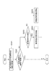
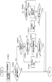
図5は、本実施形態に適用可能な画像形成システムを示すブロック図である。本実施形態における画像形成システムは、電子写真方式を用いて記録媒体に画像を形成する画像形成装置506と、入力画像データを画像形成装置が出力可能な画像データに変換する画像処理装置500とからなる。画像処理装置500と画像形成装置506は無線通信等のインタフェース又は回路によって接続されている。画像処理装置500は例えば一般的なパーソナルコンピュータにインストールされたプリンタドライバである。その場合、以下に説明する画像処理装置500内の各部は、コンピュータが所定のプログラムを実行することにより実現される。ただし、画像形成装置506が画像処理装置500を含む構成としてもよい。
<First Embodiment>
FIG. 5 is a block diagram showing an image forming system applicable to the present embodiment. The image forming system in this embodiment includes an
[画像処理装置]
画像処理装置500は、画像入力部501、色変換処理部502、色分解処理部503、量子化処理部504、細線処理部505、紙情報取得部508、画像出力509を有する。
[Image processing device]
The
画像入力部501では、画像形成装置506が印刷対象とする入力画像データが入力される。ここでは、R(レッド)、G(グリーン)、B(ブルー)からなるデジタルな入力画像データが入力されるとする。
In the
色変換処理部502は、入力画像の画像信号を、デバイスに非依存な色空間(例えば、CIE L*a*b*やCIE XYZ)にマッピングする。一般にデジタルな画像データの色再現範囲よりプリンタ等の画像形成装置506が再現可能な色再現範囲の方が狭い。そのため色変換処理部502は、入力画像データを画像形成装置506が再現可能な色再現範囲に色圧縮する変換処理を行う。ここでは色変換処理は、RGB値からL*a*b*値の対応が記載されたルックアップテーブル(LUT)に基づいて行われる。ただしこれに限定されるものではなく、マトリクス演算でも構わない。
The color
色分解処理部503は、色変換処理部502により出力されたデバイスに非依存な色空間の値から、画像形成装置506に搭載されている各色材色の信号値に変換が行われる。画像形成装置506は、C(シアン)、M(マゼンタ)、Y(イエロー)、K(ブラック)の色材を有するとする。色分解処理部503は、L*a*b*値とCMYK値との対応が記載された色分解ルックアップテーブル(LUT)507を参照して、各CMYKの信号値に変換し、各色に対応する色分解後画像データを出力する。ここで得られる各色の色分解後画像データは、8ビット(256階調)の画像データであるとする。
The color
量子化処理部504は、色分解処理部503から出力された各色色分解後画像データに対して量子化処理を行う。本実施形態において量子化処理部504は、8ビット(256階調)の色分解後画像データを画素毎に4ビット(0〜16の画素値からなる17階調)の量子化後画像データに変換する。
The
細線処理部505は、紙情報取得部508から、画像形成装置506が出力する紙の周波数特性を示す紙情報を取得し、各色の量子化後画像データに対して、出力する紙の周波数特性に応じた細線処理を行う。細線処理とは、量子化後画像データにおいて細線を形成する細線画素または、細線画素の近傍画素の画素値を補正することを意味する。細線処理部の処理内容の詳細は後述する。
The thin
画像出力部509は、細線処理部505から出力された各色の画像データを、画像形成装置506における露光部を制御するための露光信号データに変換する。本実施形態において画像出力部509は、多階調からなる画像データを露光走査距離に置き換えるパルス幅変調処理(「PWM処理」とも呼ぶ)を施す。
The
図16は、本実施形態に適用可能な画像形成システムの処理の流れを表すフローチャートである。まず画像入力部501にて画像データを取得し、画像データサイズに対応して確保されたメモリ領域に画像データを格納する(S1601)。次に、色変換処理部502にて、S1601で取得した入力画像の画像信号をデバイスに非依存な色空間にマッピングし、上記メモリ領域のデータを更新する(S1602)。色分解処理部503にて、S1602で変換されたデバイス非依存のデータから各色材色の記録量に対応する信号値に変換し、上記メモリ領域のデータを更新する(S1603)。さらに、S1603で色分解処理された色材色の信号値に対して、量子化処理部504で量子化処理を行い、上記メモリ領域のデータを更新する(S1604)。量子化処理後のデータに対して、細線処理部505にて上述した細線処理を実施し、上記メモリ領域のデータを更新する(S1605)。最後に、画像出力部509で、細線処理後のデータに対してPWM処理を行い、画像形成装置506に送る。ここでは、処理ステップが進むたびにメモリ内容を更新する例で説明したが、処理毎に異なるメモリ領域を確保してそれぞれ格納しても良い。
FIG. 16 is a flowchart showing the flow of processing of the image forming system applicable to this embodiment. First, image data is acquired by the
[画像形成装置]
図6は、本実施形態に適用可能な電子写真方式の画像形成装置506の構成を示すブロック図である。画像形成装置506は、露光部であるレーザダイオード6001とポリゴンミラー6002、像担持体である感光ドラム6003、除電器6004、帯電器6005、現像器6006を有する。さらに画像形成装置506は転写工程を行う、一次転写器6008、中間転写ベルト6007、レジストローラ6014、二次転写器6009を有する。また定着器6011により定着工程が施される。感光ドラムクリーナ6012、中間転写ベルトクリーナ6018はそれぞれ、感光体、中間転写ベルトに残留したトナーを取り除く。図6が示す1ドラム型の場合、複数色に対応する現像器が、レーザダイオード、ポリゴンミラー、感光ドラム、露光器、帯電器、一次転写器、感光ドラムクリーナを共有している。以下に、画像形成装置506におより画像が出力される工程を説明する。
[Image forming apparatus]
FIG. 6 is a block diagram illustrating a configuration of an electrophotographic
感光ドラム6003は、除電器6001により均一に除電された後、帯電器6005により均一に帯電される。レーザダイオード6001は、画像処理装置500で決定した露光信号データに基づいてレーザ光を発光する。レーザ光は、ポリゴンミラー6002、fθレンズ(不図示)を経て、矢印方向に回転している感光ドラム6003上に露光走査される。これにより感光ドラム6003上には静電潜像が形成される。その後静電潜像は、現像部6006から供給されるトナーによってトナー像として現像される。現像されたトナー像は、複数のローラ間に加張されて無端駆動される中間転写ベルト6007上に、一次転写器6008により転写される。
The
この動作を、各色の現像ユニット(シアン6006C、マゼンタ6006M、イエロー6007Y、ブラック6006K)を切り換えながら繰り返し、中間転写ベルト6007上に順次転写された複数色からなるカラーのトナー像を形成する。
This operation is repeated while switching the development units (
一方、記録媒体6010は給紙トレイ6013からレジストローラ6014まで搬送され、レジストローラ6014により二次転写器6009に搬送される。そして、中間転写ベルト6007上に転写されたカラーのトナー像は、二次転写器6009により搬送された記録媒体6010に転写される。定着器6011がトナー像を記録媒体6010上に定着させる。排紙ローラ6015にて排紙トレイ6016上に画像が形成された記録媒体6010が排出される。
On the other hand, the
なお、感光ドラム6003上に残った残留トナーは、感光ドラムクリーナ6012で掻き落とされ、回収される。また、転写材6010が分離された後、残留している中間転写ベルト6007上の残留トナーは、ブレード等の中間転写ベルトクリーナ6018によって掻き落とされる。
The residual toner remaining on the
尚、本実施形態では1ドラム型の電子写真方式の画像形成装置506の一例を示したが、複数色の現像器ごとにそれぞれの機構を有しているタンデム型の電子写真方式でも実施可能である。
In this embodiment, an example of the one-drum type electrophotographic
ここで、紙の周波数特数と細線画像の再現性について説明する。 Here, the frequency characteristic of the paper and the reproducibility of the thin line image will be described.
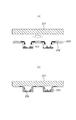
まず、細線画像の再現性低下を招く転写不良には、様々な要因が挙げられている。その一つとして転写される紙と中間転写体上のトナーとの間のエアーギャップが挙げられる。図1は、転写前後の中間転写体から紙へのトナーの移動を示す、断面方向からの概念図である。図1(a)は転写前、図1(b)は転写後の様子をそれぞれ表している。中間転写体101上のトナー103が紙102に転写される。図中に図示しないが、表面に凹凸の少ない平滑な用紙であれば、エアーギャップは場所によらずほぼ同じ程度なので、トナー層が紙に均一に転移する。しかし、図1に示すような表面凹凸(表面粗さ)の大きな紙では、紙の凹部でエアーギャップが広がり、転写電界が弱まるため、凹部にトナーが十分に転写されず、中間転写体上の残留トナー104が残ってしまう。
First, various factors are cited as a transfer defect that causes a decrease in reproducibility of a fine line image. One example is an air gap between the paper to be transferred and the toner on the intermediate transfer member. FIG. 1 is a conceptual diagram from the cross-sectional direction showing the movement of toner from the intermediate transfer member to the paper before and after the transfer. FIG. 1A shows a state before transfer, and FIG. 1B shows a state after transfer. The
次に、細線画像の再現性低下を招く定着不良についても、さまざまな要因が挙げられるが、紙の表面凹凸による定着不良について説明する。図2は、定着工程における紙上でのトナーの変形を示す、断面方向からの概念図である。図2(a)は定着ニップでの挙動、図2(b)は定着後の様子をそれぞれ表している。定着部材201は、紙202に対して加熱、加圧により定着する。図中に図示しないが、表面に凹凸の少ない平滑な紙であれば、トナーにかかる圧力も熱量も場所によらずほぼ同じなので、トナー層が紙に均一に定着する。しかし、図2に示すような表面凹凸の大きな紙では、定着ニップ内でトナーが加熱、加圧され、トナーが溶融して紙上に定着する過程で、凸部のトナー203は図2(a)の矢印に示すように定着部材からの圧力で凹部方向に掃き寄せられる。また凹部のトナー204は定着部材と接触しないため、十分に溶融および圧着されない。結果として、凸部ではトナーの透けが発生し、凹部ではトナーが十分に潰されなかったことによりトナー間に隙間が発生する。このため、紙表面が十分に被覆されないという現象が発生する。
Next, although there are various factors in the fixing failure that causes a decrease in reproducibility of the thin line image, the fixing failure due to the surface unevenness of the paper will be described. FIG. 2 is a conceptual view from the cross-sectional direction showing the deformation of the toner on the paper in the fixing step. FIG. 2A shows the behavior at the fixing nip, and FIG. 2B shows the state after fixing. The fixing
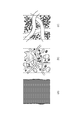
このように、紙の表面凹凸が大きいために転写不良、定着不良が発生し、細線再現性が低下する。さらに細線再現性は、紙の繊維の細かさによっても異なる。図3は、試料を光学顕微鏡等で拡大して観察した様子を示す概念図である。図3(a)は、表面凹凸の少ない平滑な紙に細線画像を印刷した場合の概念図である。図3(b)は、細い繊維の紙に細線画像を印刷した場合の概念図である。図3(c)は、太い繊維の紙に細線画像を印刷した場合の概念図である。一般的に、紙の表面凹凸の周波数特性として、細い繊維の紙では高周波成分が多く振幅が低い傾向があり、太い繊維の紙では低周波成分が多く振幅が高い傾向がある。点線の内側が本来、細線が形成される領域である。平滑な紙を用いた図3(a)では、本来細線が形成される領域に十分なトナー量で細線が形成されていることがわかる。表面の凹凸のある図3(b)、図3(c)では、上述した通り、転写工程で紙上に転写されるトナー量は、平滑な紙の場合と比べて少なくなる。また、定着工程において繊維上のトナーは繊維間に掃き寄せられ、繊維間のトナーは溶融や圧着が不十分になる。図3(b)では、トナーの透けが発生する凸部は高周波に存在し、凹凸の振幅が小さいため定着部材はトナーに接触してトナーが薄く潰される。図3(c)では、トナーの透けが発生する凸部は低周波に存在し、凹凸の振幅が大きいため定着部材のトナーに接触せずトナーが十分に潰されない。なお上述した通り、一般的には、紙の表面凹凸は繊維の太さに応じて、低周波かつ高振幅、または、高周波かつ低振幅になりやすいが、紙の種類によってはこの限りでは無いと考えられる。紙によって、多様な周波数特性の表面凹凸をもつ。 As described above, since the surface unevenness of the paper is large, transfer failure and fixing failure occur, and the fine line reproducibility deteriorates. Furthermore, fine line reproducibility also varies depending on the fineness of the paper fibers. FIG. 3 is a conceptual diagram illustrating a state in which a sample is observed with an optical microscope or the like. FIG. 3A is a conceptual diagram when a fine line image is printed on a smooth paper with few surface irregularities. FIG. 3B is a conceptual diagram when a fine line image is printed on a thin fiber paper. FIG. 3C is a conceptual diagram when a fine line image is printed on thick fiber paper. In general, the frequency characteristics of the paper surface unevenness tend to have a high frequency component and a low amplitude in the thin fiber paper, and a high frequency component and a high amplitude in the thick fiber paper. The area inside the dotted line is the area where the thin line is originally formed. In FIG. 3A using smooth paper, it can be seen that fine lines are formed with a sufficient amount of toner in a region where fine lines are originally formed. In FIGS. 3B and 3C where the surface is uneven, as described above, the amount of toner transferred onto the paper in the transfer process is smaller than that of smooth paper. In the fixing process, the toner on the fibers is swept between the fibers, and the toner between the fibers is not sufficiently melted or pressed. In FIG. 3B, the convex portion where toner see-through occurs exists at a high frequency, and the amplitude of the concave and convex portions is small, so that the fixing member comes into contact with the toner and the toner is thinly crushed. In FIG. 3C, the convex portion where toner see-through occurs exists at a low frequency, and the amplitude of the concave and convex portions is large, so that the toner does not contact the toner of the fixing member and the toner is not sufficiently crushed. As described above, in general, the surface irregularities of the paper are likely to be low frequency and high amplitude, or high frequency and low amplitude depending on the thickness of the fiber, but this is not limited depending on the type of paper. Conceivable. Depending on the paper, it has surface irregularities with various frequency characteristics.
図4は、紙の周波数特性によって異なる細線再現性を模式的に示した図である。図4(a)は入力信号が100%の細線画素を含む画像40が入力された場合、図4(b)は入力信号が60%の細線画素を含むハーフトーン画像41が入力された場合の例を示す。画像401と405は高周波かつ高振幅な紙の場合、画像402と406は低周波かつ高振幅な紙の場合、画像403と407は高周波かつ低振幅な紙の場合、画像404と408は低周波かつ低振幅な紙の場合の例である。
FIG. 4 is a diagram schematically showing reproducibility of fine lines depending on the frequency characteristics of paper. 4A shows a case where an
図3(b)が示す高周波かつ低振幅の周波数特性をもつ紙に細線画像を出力した概念図は細線画像403であり、画像40より濃度の低い細線となる。画像401は画像403と同程度の高周波な表面凹凸であり、画像403より高振幅の紙の場合を示している。同程度高周波でより高振幅な周波数特性をもつ紙に細線を含む画像を出力すると、より濃度が低下し、さらに細線再現性が低くなってしまう。また、図3(c)が示す低周波かつ高振幅の周波数特性をもつ紙に細線画像を出力した概念図が402であり、画像40より細くうねりのある細線となる。画像404は402と同程度の低周波な表面凹凸であり、画像402より低振幅の紙の場合を示している。同程度低周波でより低振幅な表面凹凸の紙の場合、画像402より濃度が濃いため、うねりによる細線再現性の低下が抑制される。一定以上の振幅成分がある紙の場合、細線画像は濃度が薄くなってしまう。また、表面凹凸が低周波な周波数特性をもつ紙の場合、細くうねりのある細線になり、表面凹凸が高周波な周波数特性の紙では濃度の低い細線となる。さらに、表面凹凸の振幅によって線の細りの程度、濃度低下の程度が異なる。以上のように、紙の表面凹凸がもつ周波数特性によって、細線再現性が異なっていることがわかる。
A conceptual diagram in which a fine line image is output on paper having high frequency and low amplitude frequency characteristics shown in FIG. 3B is a
[紙情報取得部詳細]
紙情報取得部508が取得する画像形成装置506が出力する紙の周波数特性を示す紙情報について説明する。図7は、紙の表面凹凸を測定する方法の一例である凹凸センサを示す概念図である。凹凸センサユニット70は、対象とする紙71の表面凹凸情報を測定する。凹凸センサユニット70は、光源部703、受光部702を有する。光源部703は、画像形成装置506が有するレーザ光のようにスポット径の小さい光ビームを発する構成であることが望ましい。また、表面がコートされていない非コート紙では表面反射光の強度が低いため、受光部702は光感度の高い受光素子であることが望ましい。図7における点線は、光の照射された領域の紙の法線方向を示しおり、矢印は光源部703による光ビームの進行方向を示している。図からわかるように、図7(a)の状態では表面反射光が受光部702と異なる方向に反射する。図7(a)が示す状態から紙を搬送し(あるいは凹凸センサユニット70を走査し)、図7(b)が示す状態に遷移すると表面反射光が受光部702で受光される。図8は、図7に示した凹凸センサユニット70における受光部702で受光した表面反射光の強度の一例を示すグラフである。測定結果801は、表面凹凸が高周波かつ振幅の小さい周波数特性の紙を測定した結果、測定結果802は表面凹凸が低周波かつ振幅が大きい周波数特性の紙を測定した結果を示している。紙の表面凹凸の周波数が高いほど光強度変化の周期が短く、振幅が大きいほど表面反射光の強度変化の振幅が大きいことがわかる。この表面反射光の強度変化を周波数解析することにより、間接的に紙の表面凹凸の周波数特性を得ることができる。尚、表面反射光の強度の絶対値は紙の反射率自体に依存するため、周波数解析時に直流成分は除外する。また、凹凸センサユニット70を画像形成装置の内部に具備しておき、紙を通紙してセンシングしても良いし、凹凸センサユニット70を画像形成装置とは別構成にしておきセンサユニット側を走査させても良い。
[Details of the paper information acquisition unit]
The paper information indicating the frequency characteristics of the paper output by the
紙凹凸情報の取得方法は、上述した方式に限定されず、面発光式の光源を用いて紙を照射し2次元センサで撮像する構成でも良い。もちろん、良く知られるレーザ顕微鏡、光干渉方式の表面形状測定器、AFM、三次元デジタイザ等の表面形状測定器を利用しても良い。さらに、画像処理装置500において選択可能な紙に凹凸情報を付加しておき、選択された紙に応じて自動的に紙の表面凹凸情報を取得しても良いし、ユーザによって紙の表面凹凸情報が入力される方式でも構わない。
The method for acquiring the paper unevenness information is not limited to the above-described method, and may be configured to irradiate paper using a surface-emitting light source and capture an image with a two-dimensional sensor. Of course, a well-known surface microscope such as a laser microscope, an optical interference type surface profiler, an AFM, a three-dimensional digitizer, or the like may be used. Furthermore, the unevenness information may be added to the selectable paper in the
[細線処理部詳細]
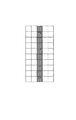
紙の周波数特性に応じた細線処理部505における補正処理について詳細に説明する。上述した通り、紙の表面凹凸の周波数特性によって細線の印刷結果が異なる。紙の表面凹凸が低周波の場合は本来意図した線幅より細くなり、紙の表面凹凸が高周波の場合は本来意図した線濃度より薄くなる傾向がある。そこで、紙の表面凹凸の周波数特性に応じて補正することで、高品質な細線画像を出力する。図9は、補正方法を決定する処理の流れを示すフローチャートである。
[Details of thin line processing section]
The correction process in the thin
まずステップS901において、上述した方法を利用して出力する紙の表面凹凸の周波数特性を取得する。センサユニット70が測定した結果から、紙の表面凹凸の振幅および周波数を示す情報を取得する。次にステップS902において、対象とするいずれの周波数においても振幅が所定の閾値以下、つまり表面粗さが所定値以下かどうかを判定する。S902において、出力する紙について、いずれの周波数においても振幅が所定の閾値以下であると判定された場合、すなわち表面の平滑な紙の場合、補正処理を行う必要が無いため補正処理を完了する。ステップS902において、いずれかの周波数において振幅が所定の閾値より大きいと判定された場合、すなわち表面の粗い紙が利用される場合、補正処理を行う必要がある。ステップS902における閾値は必ずしも全ての周波数で一定値である必要はなく、周波数帯毎に異なる閾値を設定しておいても良い。ステップS902で補正処理を行う必要があると判定された場合、ステップS903に進む。
First, in step S901, the frequency characteristics of the surface irregularities of the paper to be output using the method described above are acquired. Information indicating the amplitude and frequency of the surface irregularities of the paper is acquired from the measurement result of the
ステップS903において、予め設定された所定の周波数より低い周波数帯において所定の閾値より高い振幅成分が存在するか否かを判定する。ステップS903で低周波帯域に高い振幅成分が存在すると判定された場合、ステップS904に進み、低周波紙用の補正処理を実行する。ステップS903で低周波帯域に高い振幅成分が存在しないと判定された場合、すなわち高い振幅成分は高周波帯域側に存在すると判定された場合は、ステップS905に進み、高周波紙用の補正処理を実行する。 In step S903, it is determined whether an amplitude component higher than a predetermined threshold exists in a frequency band lower than a predetermined frequency set in advance. If it is determined in step S903 that a high amplitude component exists in the low frequency band, the process proceeds to step S904, and correction processing for low frequency paper is executed. If it is determined in step S903 that there is no high amplitude component in the low frequency band, that is, if it is determined that the high amplitude component exists on the high frequency band side, the process proceeds to step S905, and correction processing for high frequency paper is executed. .
図10〜13を参照して、ステップS904の処理内容を説明する。上述した通り、紙の表面凹凸が低周波な場合、平滑紙と同様の条件で印刷を行うと、本来意図した細線画像より細い線が印刷されてしまう。そこで、量子化処理部504で量子化された画像データに基づいて生成される露光信号データにおいて、細線を太くするように画素値を変更する。つまり細線処理部505は、露光信号データが示す露光幅が太くなるように画素値を変更する。なお、細線処理部505は、画素値0の画素に対しては処理を行わない。
The processing content of step S904 will be described with reference to FIGS. As described above, when the surface unevenness of the paper has a low frequency, if printing is performed under the same conditions as for smooth paper, a finer line than the originally intended thin line image is printed. Therefore, in the exposure signal data generated based on the image data quantized by the
図10は、細線画素を含む画像に対して量子化処理部504が量子化処理した量子化後画像データの一例である。図10が示す量子化後画像データの各画素(格子)について、画素値に応じて画像形成装置は16段階で出力することができる。量子化画像データにおいて、塗りつぶされた領域が細線を形成する細線画素である。細線画素はそれぞれ画素値8であり、それ以外の画素の画素値は0である場合を例に示す。図11は、図10が示す画像データに対してPWM処理することにより得られる露光信号データの例を示す。図11(a)は、ステップS902で補正処理を行う必要が無いと判定された平滑紙の場合の露光信号データを示している。レーザ光の主走査方向(図中の横方向)に対して1画素のうち幅50%が露光される露光信号データとなっている。図11(b)は、ステップS904における低周波紙用の補正処理を行った場合の露光信号データを示しており、1画素につき80%の幅が露光される。主走査方向に長く露光されるため、潜像像や現像像では入力された細線画像より太い線となるが、前述の通り転写工程、定着工程において線が細くなるため、記録媒体上では入力された細線画像と同等の太さの線が印刷されることになる。尚、100%を超えるPWM処理は出来ないため、画素値が16である画素が形成する細線については、図11(b)が示す補正処理はできない。そこで、1画素に対応する露光が100%以上必要な場合の例を、図12、図13を用いて説明する。図10と同様の細線画素を含む画像デ―タであり、細線画素の画素値が16であったとする。図12は、画素値16の画素が細線を形成する量子化後画像データに対して、細線処理部505が補正処理した結果得られるデ―タを示す。図12の中心列における画素の画素値16であり、中心列の両脇の列に位置する細線画素の近傍の画素はそれぞれ画素値が8である。つまり、本来細線を形成する画素の近傍画素を露光することにより、露光幅が大きくなるように補正処理をする。図13に、図12が示す画像データに基づいて生成された露光信号データを示している。中心列が100%、両脇の列が50%露光され、細線を形成する露光信号データの合計は、入力された細線画像よりも太い線になっていることがわかる。尚、図13においてPWM処理により細線領域を判別して左寄せや右寄せを行った好ましい例を示したが、単に中央寄せのPMW処理であっても構わない。
FIG. 10 is an example of post-quantization image data obtained by the
なお、ここでは縦方向の細線を含む画像を例に示したが、横方向の細線や斜め方向の細線を含む画像でも、図12、図13で説明したような補正処理を行うことで実現可能である。さらに、紙の表面凹凸の振幅によって、細線の細くなる程度は異なるため、振幅が大きいほど露光される面積を広くするなど、振幅情報によって露光信号データの補正量を適宜決定することが望ましい。ステップS904における線を太くする処理において、補正を行う方法はこれに限定されず、例えば紙の表面凹凸の周波数特性に応じて入力画像に対して太線化の補正を行うなどの方法でも良い。 Although an image including a vertical thin line is shown as an example here, an image including a horizontal thin line or an oblique thin line can be realized by performing the correction processing described with reference to FIGS. 12 and 13. It is. Further, since the degree of thinning of the thin line varies depending on the amplitude of the surface irregularities of the paper, it is desirable to appropriately determine the correction amount of the exposure signal data based on the amplitude information, such as increasing the exposed area as the amplitude increases. In the process of thickening the line in step S904, the correction method is not limited to this. For example, a thickening correction may be performed on the input image according to the frequency characteristics of the paper surface unevenness.
次に、図14を参照して、ステップS905の処理内容を説明する。上述した通り、紙の表面凹凸が高周波な場合、平滑紙と同様の条件で印刷を行うと、本来意図した細線画像より濃度が低く印刷されてしまう。そこで、量子化処理部504から得られる量子化後画像データに対して、平滑紙の場合より細線画素の濃度を高くするように補正処理を行う。濃度を高くするということは、すなわち紙の上に転写されるトナー像を高くする処理である。例えば、露光するレーザ光の強度(以下、露光強度)を高くすることで現像されるトナー像(現像トナー像)を高くし、結果として表面凹凸の大きい紙でも紙上に転写されるトナー量を平滑紙の場合と同等程度にすることができる。なお、ステップS905において細線処理部505は、画素値0の画素に対しては処理を行わない。
Next, the processing content of step S905 will be described with reference to FIG. As described above, when the surface unevenness of the paper is high frequency, if printing is performed under the same conditions as smooth paper, the density is printed lower than the originally intended fine line image. Therefore, correction processing is performed on the quantized image data obtained from the
図14は、この露光強度を変更する処理であるパルス強度変調処理(PAM処理)を行った場合の、露光信号データの例である。図14(a)は、S902で補正処理を行う必要が無いと判定された平滑紙の場合の露光信号データ(パルス信号値)を示している。図14(b)は、ステップS905における高周波紙用の補正処理を行った場合の露光信号データを示しており、図14(a)より露光強度が高い値になっている。上述した通り、現像されるトナー像は平滑紙の場合よりトナーの高さが高くなり、転写工程、定着工程を経て、記録媒体上では入力された細線画像と同等の濃度の線が印刷されることになる。現像されるトナー量を増やす処理は、PAM処理に限定されず、例えば現像バイアスを高くするなどの処理を行っても良い。紙の表面凹凸の振幅によって、細線の濃度低下の程度は異なるため、振幅が大きいほど露光強度を高くする、あるいは、現像バイアスを高くするなど、振幅情報によって現像されるトナーの補正量を適宜決定することが望ましい。 FIG. 14 is an example of exposure signal data when pulse intensity modulation processing (PAM processing), which is processing for changing the exposure intensity, is performed. FIG. 14A shows exposure signal data (pulse signal value) in the case of smooth paper that is determined not to need to be corrected in S902. FIG. 14B shows exposure signal data when the correction processing for high-frequency paper in step S905 is performed, and the exposure intensity is higher than that in FIG. As described above, the toner image to be developed has a toner height higher than that of smooth paper, and a line having the same density as the input thin line image is printed on the recording medium after the transfer process and the fixing process. It will be. The process for increasing the amount of toner to be developed is not limited to the PAM process, and a process such as increasing the development bias may be performed. Since the degree of density reduction of fine lines varies depending on the amplitude of the surface irregularities of the paper, the correction amount of the toner to be developed is appropriately determined based on the amplitude information, such as increasing the exposure intensity or increasing the developing bias as the amplitude increases. It is desirable to do.
また本実施形態では、PWM処理を行う構成を例に説明したが、これに限らない。 In this embodiment, the configuration for performing the PWM processing has been described as an example, but the present invention is not limited to this.
以上、説明した本処理を行うことで、表面凹凸が有する周波数特性が異なる紙を用いた場合に、細線画像の品位の低下を抑制することができる。 By performing the above-described processing as described above, it is possible to suppress the deterioration of the quality of the fine line image when using paper having different frequency characteristics of the surface unevenness.
<第2実施形態>
第1実施形態では、記録媒体の表面凹凸が粗い場合、画素値が0の画素を除く全ての画素に対して細線の再現性を保障するための処理(ステップS904またはステップ905)について述べた。しかしながら、細線領域以外にも同じ処理が施されるため、網点面積拡大または網点濃度上昇が発生し、入力画像によっては濃度が高くなってしまう可能性がある。これに付随し、マクロ的な濃度に非線形な変化が発生し、階調性が低下する可能性がある。
Second Embodiment
In the first embodiment, when the surface roughness of the recording medium is rough, the processing (step S904 or step 905) for ensuring the reproducibility of the thin line for all the pixels except the pixel having the pixel value of 0 has been described. However, since the same processing is performed for areas other than the thin line area, the dot area enlargement or the dot density increase occurs, and the density may increase depending on the input image. Accompanying this, there is a possibility that a non-linear change occurs in the macro density and the gradation is lowered.
そこで、本実施形態では、入力画像における細線領域を抽出し、細線領域についてのみ第1実施形態と同様の細線処理を実施する例を述べる。 Therefore, in the present embodiment, an example will be described in which a fine line region in the input image is extracted and only the fine line region is subjected to the same thin line processing as in the first embodiment.
基本的な構成や処理内容は第1実施形態と同様であるため、第1実施形態と異なる箇所についてのみ説明を行い、それ以外については説明を割愛する。 Since the basic configuration and processing contents are the same as those of the first embodiment, only the parts different from the first embodiment will be described, and the description of the other parts will be omitted.
図17は、本実施形態に適用可能な電子写真方式の画像形成装置506の構成を示すブロック図である。
FIG. 17 is a block diagram showing a configuration of an electrophotographic
[画像処理装置]
画像処理装置1700は、画像入力部1701、色変換処理部1702、像域判定部1703、色分解処理部1704、量子化処理部1705、細線処理部1706、紙情報取得部1708、画像出力部1709を有する。画像入力部1701では、第1実施形態と同様、画像形成装置506が印刷対象とするRGBの入力画像データが入力される。色変換処理部1702は、入力画像の画像信号を、CIE L*a*b*などデバイスに非依存な色空間にマッピングする。
[Image processing device]
The
本実施形態に特有の構成である像域判定部1703は、特開平5−14702号をはじめとして、数多く発明されているので詳細な説明はここでは省略するが、基本的な動作は1画素単位で細線情報かそれ以外のオブジェクトかを判定し、オブジェクトごとの信号を生成する処理のことである。この信号は、例えば、細線であれば1、細線でなければ0といった値を画素毎に付与する。このオブジェクト信号を参照することで読み取り画像の任意画素位置が細線か否かを区別できるようになる。
An image
色分解処理部1704は、色変換処理部1702により出力されたデバイスに非依存な色空間の値から、画像形成装置506に搭載されている各色材色CMYKの信号値に変換が行われる。色分解処理部1704は、L*a*b*値とCMYK値との対応が記載された色分解LUT1707を参照して、各CMYKの信号値に変換し、各色に対応する色分解後画像データを出力する。ここで得られる各色の色分解後画像データは、8ビット(256階調)の画像データであるとする。
The color
量子化処理部1705は、色分解処理部1704から出力された各色色分解後画像データに対して量子化処理を行う。本実施形態において量子化処理部1705は、8ビット(256階調)の色分解後画像データを画素毎に4ビット(0〜16の画素値からなる17階調)の量子化後画像データに変換する。
The
細線処理部1706は、紙情報取得部1708から、画像形成装置506が出力する紙の周波数特性を示す紙情報を取得し、各色の量子化後画像データに対して、出力する紙の周波数特性に応じた細線処理を行う。この処理において、像域判定部1703で生成された細線情報か否かの信号に応じて、細線処理を行うかどうかを決定する。尚、細線と判定された画素に対する細線処理は第1実施形態と同様の処理を実施し、細線でないと判定された画素に対しては処理を行わない。
The thin
画像出力部1709は、細線処理部1706から出力された各色の画像データを、画像形成装置506における露光部を制御するための露光信号データに変換する。本実施形態において画像出力部1709は、多階調からなる画像データを露光走査距離に置き換えるPWM処理を施す。
The
図18は、本実施形態に適用可能な画像形成システムの処理の流れを表すフローチャートである。まず画像入力部1701にて画像データを取得し、画像データサイズに対応して確保されたメモリ領域に画像データを格納する(S1801)。次に、色変換処理部1702にて、S1801で取得した入力画像の画像信号をデバイスに非依存な色空間にマッピングし、上記メモリ領域のデータを更新する(S1802)。像域判定部1703にて、S1803で変換されたデバイス非依存のデータに対し、1画素単位で細線情報かそれ以外のオブジェクトかを判定し、細線であれば1、細線でなければ0の信号を画素毎に付与する(S1803)。
FIG. 18 is a flowchart showing the flow of processing of the image forming system applicable to this embodiment. First, image data is acquired by the
色分解処理部1704で、S1803で変換されたデバイス非依存のデータを各色材色の記録量に対応する信号値に変換し、上記メモリ領域のデータを更新する(S1804)。さらに、S1804で色分解処理された各色材色の信号値に対して、量子化処理部1705で量子化処理を行い、上記メモリ領域のデータを更新する(S1805)。量子化処理後のデータに対して、細線処理部1706にて上述した細線処理を実施し、上記メモリ領域のデータを更新する(S1806)。最後に、画像出力部1709で、細線処理後のデータに対してPWM処理を行い、画像形成装置506に送る(S1807)。ここでは、処理ステップが進むたびにメモリ内容を更新する例で説明したが、処理毎に異なるメモリ領域を確保してそれぞれ格納しても良い。
The color
図19は、S1806の細線処理の詳細を説明するフローチャートである。 FIG. 19 is a flowchart for explaining the details of the thin line processing in S1806.
まずステップS1901において、第1実施形態同様、出力する紙の表面凹凸の周波数特性を取得する。次にステップS1902において、対象とするいずれの周波数においても振幅が所定の閾値以下、つまり表面粗さが所定値以下かどうかを判定する。S1902において、出力する紙について、いずれの周波数においても振幅が所定の閾値以下であると判定された場合、すなわち表面の平滑な紙の場合、補正処理を行う必要が無いため補正処理を完了する。ステップS1902において、いずれかの周波数において振幅が所定の閾値より大きいと判定された場合、すなわち表面の粗い紙が利用される場合、補正処理を行う必要がある。ステップS1902における閾値は必ずしも全ての周波数で一定値である必要はなく、周波数帯毎に異なる閾値を設定しておいても良い。ステップS1902で補正処理を行う必要があると判定された場合、ステップS1903に進む。 First, in step S1901, the frequency characteristics of the surface irregularities of the output paper are acquired as in the first embodiment. Next, in step S1902, it is determined whether the amplitude is equal to or smaller than a predetermined threshold value, that is, the surface roughness is equal to or smaller than a predetermined value at any target frequency. If it is determined in step S1902 that the amplitude of the output paper is equal to or smaller than a predetermined threshold value at any frequency, that is, if the paper has a smooth surface, the correction process is not necessary and the correction process is completed. If it is determined in step S1902 that the amplitude is greater than a predetermined threshold value at any frequency, that is, if rough paper is used, correction processing must be performed. The threshold value in step S1902 does not necessarily have to be a constant value for all frequencies, and a different threshold value may be set for each frequency band. If it is determined in step S1902 that correction processing is necessary, the process proceeds to step S1903.
ステップS1903において、予め設定された所定の周波数より低い周波数帯において所定の閾値より高い振幅成分が存在するか否かを判定する。ステップS1903で低周波帯域に高い振幅成分が存在すると判定された場合、ステップS1904に進み、画素単位で細線か否かの判定処理を行う。ステップS1904で対象画素が細線と判定された場合、低周波紙用細線処理を行う(ステップS1905)。ステップS1904で対象画素が細線でないと判定された場合、細線処理を行わない。全画素処理済みか否かを判定し(ステップS1906)、処理が終わっていなければ次の画素に移動し(ステップS1907)、ステップS1904に戻る。以降、同様に処理を繰り返し、S1906で全画素処理済みとなれば、細線処理を完了する。 In step S1903, it is determined whether there is an amplitude component higher than a predetermined threshold in a frequency band lower than a predetermined frequency set in advance. If it is determined in step S1903 that a high amplitude component exists in the low frequency band, the process advances to step S1904 to determine whether or not the pixel is a thin line. If it is determined in step S1904 that the target pixel is a thin line, low-frequency paper thin line processing is performed (step S1905). If it is determined in step S1904 that the target pixel is not a fine line, the fine line process is not performed. It is determined whether or not all the pixels have been processed (step S1906). If the processing has not been completed, the process moves to the next pixel (step S1907), and the process returns to step S1904. Thereafter, the processing is repeated in the same manner. When all the pixels have been processed in S1906, the thin line processing is completed.
ステップS1903で低周波帯域に高い振幅成分が存在しないと判定された場合、すなわち高い振幅成分は高周波帯域側に存在すると判定された場合は、ステップS1908に進み、ステップS1908に進み、画素単位で細線か否かの判定処理を行う。ステップS1908で対象画素が細線と判定された場合、高周波紙用細線処理を行う(ステップS1909)。ステップS1908で対象画素が細線でないと判定された場合、細線処理を行わない。全画素処理済みか否かを判定し(ステップS1910)、処理が終わっていなければ次の画素に移動し(ステップS1911)、ステップS1908に戻る。以降、同様に処理を繰り返し、S1910で全画素処理済みとなれば、細線処理を完了する。 If it is determined in step S1903 that a high amplitude component does not exist in the low frequency band, that is, if it is determined that a high amplitude component exists on the high frequency band side, the process proceeds to step S1908, and the process proceeds to step S1908. Whether to determine whether or not. If it is determined in step S1908 that the target pixel is a thin line, high-frequency paper thin line processing is performed (step S1909). If it is determined in step S1908 that the target pixel is not a fine line, the fine line process is not performed. It is determined whether or not all the pixels have been processed (step S1910). If the processing has not been completed, the process moves to the next pixel (step S1911), and the process returns to step S1908. Thereafter, the same processing is repeated, and if all pixel processing is completed in S1910, the thin line processing is completed.
ステップS1905の低周波紙用細線処理、ステップS1909の高周波紙用細線処理、さらには、細線処理を行わない場合についての詳細な処理に関しては、第1実施形態と同様のため説明を割愛する。 Since the thin line processing for low-frequency paper in step S1905, the thin line processing for high-frequency paper in step S1909, and the detailed processing in the case where the thin line processing is not performed are the same as those in the first embodiment, description thereof will be omitted.
尚、像域判定部1703では色変換処理部1702でL*a*b*等のデバイスに非依存な色空間にマッピングされたデータに対して判定処理を行う例を説明したが、これに限定されない。例えば、RGB等の入力画像データに対して処理を行っても良いし、色分解処理部1704で処理されたCMYKのデータに対して処理を行っても良い。
Note that the image
以上、説明した本処理を行うことで、表面凹凸が有する周波数特性が異なる紙を用いた場合に、細線画像の品位の低下を抑制した上で、画像濃度の変動を抑制することができる。 By performing the above-described processing as described above, when using paper having different frequency characteristics of the surface unevenness, it is possible to suppress a change in image density while suppressing a decrease in the quality of the fine line image.
<変形例>
第1実施形態では、表面凹凸の周波数特性が低周波な紙に画像を形成する場合に、細線を太線化する処理を説明したが、使用する紙によっては紙の繊維方向(表面凹凸)に異方性がある場合がある。特に、量子化された細線画像においては、現像されるトナー領域を縦方向にも横方向にも広げることが可能だが、紙の表面凹凸の異方性との組み合わせによって、太線化の効果の大小は異なる。そこで、表面凹凸の異方性の大きい紙を利用する場合における、より好適な処理方法を以下に説明する。
<Modification>
In the first embodiment, the processing for thickening thin lines when forming an image on paper with low frequency characteristics of the surface unevenness has been described. However, depending on the paper used, the fiber direction (surface unevenness) of the paper differs. There may be a direction. In particular, in a quantized thin line image, the developed toner area can be expanded both in the vertical direction and in the horizontal direction. Is different. Therefore, a more preferable processing method in the case of using paper with large surface irregularities is described below.
図9のステップS901において、紙の表面凹凸の周波数特性を取得する際に、紙の表面凹凸の異方性情報も同時に取得する。例えば、図7の凹凸センサユニットを用いて、使用する紙を縦方向、横方向にそれぞれ走査して、縦方向の表面凹凸と横方向の表面凹凸をそれぞれ取得する。または、第1実施形態に記載した別の表面凹凸取得方法である2次元センサ、表面形状測定器の利用や、ユーザによって紙の凹凸情報が入力される方式でも構わない。 In step S901 in FIG. 9, when acquiring the frequency characteristics of the paper surface unevenness, the anisotropic information of the paper surface unevenness is also acquired simultaneously. For example, by using the unevenness sensor unit of FIG. 7, the paper to be used is scanned in the vertical direction and the horizontal direction, respectively, and the vertical surface unevenness and the horizontal surface unevenness are respectively acquired. Alternatively, another method for obtaining surface irregularities described in the first embodiment, such as a two-dimensional sensor or a surface shape measuring instrument, or a method in which paper irregularity information is input by a user may be used.
次に、ステップS903にて、低周波成分が検出された場合、縦方向と横方向のどちらの振幅の方が高いかを判定する。縦方向の振幅の方が横方向の振幅より高い場合、縦方向に現像トナー領域を広げ、横方向の振幅の方が縦方向の振幅より高い場合、横方向に現像トナー領域を広げる。 Next, when a low frequency component is detected in step S903, it is determined which amplitude in the vertical direction or the horizontal direction is higher. When the amplitude in the vertical direction is higher than the amplitude in the horizontal direction, the developing toner region is expanded in the vertical direction, and when the amplitude in the horizontal direction is higher than the amplitude in the vertical direction, the developing toner region is expanded in the horizontal direction.
図15は、紙の表面凹凸に異方性がある場合において、現像トナー領域を広げる方向を説明するための概念図を示す。図15(a)は、縦方向の繊維が多い紙の場合、すなわち縦方向の振幅の方が横方向の振幅より高い場合である。横方向に現像トナー領域を広げても、転写、定着工程において、紙上では紙繊維によって透けたり掃き寄せられたりするため、縦方向に広げることでより効率的に紙上での被覆率を向上させるができる。同様に、図15(b)は、横方向の繊維が多い紙の場合、すなわち横方向の振幅の方が縦方向の振幅より高い場合である。縦方向に現像トナー領域を広げても、転写工程、定着工程において、紙上では繊維によって透けたり掃き寄せられたりするため、横方向に広げることでより効率的に紙上での被覆率を向上させる。 FIG. 15 is a conceptual diagram for explaining the direction in which the developing toner area is widened when there is anisotropy in the paper surface unevenness. FIG. 15A shows the case of paper with a lot of fibers in the vertical direction, that is, the case where the amplitude in the vertical direction is higher than the amplitude in the horizontal direction. Even if the development toner area is expanded in the horizontal direction, it is transparent or swept away by the paper fiber on the paper in the transfer and fixing process, so that the coverage on the paper can be improved more efficiently by expanding in the vertical direction. it can. Similarly, FIG. 15B shows a case where the paper has many fibers in the horizontal direction, that is, a case where the amplitude in the horizontal direction is higher than the amplitude in the vertical direction. Even if the developing toner area is expanded in the vertical direction, the paper is transparent or swept away by the fibers in the transfer process and the fixing process. Therefore, the covering ratio on the paper can be improved more efficiently by expanding in the horizontal direction.
尚、現像トナー領域の広げ方は第1実施形態に記載の方法を利用できる。 Note that the method described in the first embodiment can be used for expanding the developing toner area.
<その他の実施形態>
本発明の目的は前述した実施例の機能を実現するソフトウエアのプログラムコードを記録した記録媒体を、システム、情報処理装置に供給し、それらのコンピュータ(またはCPUまたはMPU)がプログラムコードを読み出し実行することでも達成され得る。この場合、記憶媒体から読み出されたプログラムコード自体が前述した実施形態の機能を実現することとなり、そのプログラムコードを記憶したコンピュータ可読記憶媒体は本発明を構成することになる。
<Other embodiments>
The object of the present invention is to supply a recording medium storing software program codes for realizing the functions of the above-described embodiments to a system and an information processing apparatus, and those computers (or CPUs or MPUs) read and execute the program codes. Can also be achieved. In this case, the program code itself read from the storage medium realizes the functions of the above-described embodiments, and the computer-readable storage medium storing the program code constitutes the present invention.
プログラムコードを供給するためのコンピュータ可読記憶媒体としては、例えば、ハードディスク、光ディスク、光磁気ディスク、CD−ROM、磁気テープ、不揮発性のメモリカード、ROM、DVDなどを用いることができる。 As a computer-readable storage medium for supplying the program code, for example, a hard disk, an optical disk, a magneto-optical disk, a CD-ROM, a magnetic tape, a nonvolatile memory card, a ROM, a DVD, or the like can be used.
また、コンピュータが読み出したコンピュータプログラムコードを実行することにより、前述した実施例の機能が実現される。さらにそのプログラムコードの指示に基づき、コンピュータ上で稼動しているOSなどが実際の処理の一部または全部を行うこともできる。その処理によって前述した実施例の機能が実現される場合も含まれることは言うまでもない。 The functions of the above-described embodiments are realized by executing the computer program code read by the computer. Furthermore, based on the instruction of the program code, an OS running on the computer can perform part or all of the actual processing. Needless to say, the process includes the case where the functions of the above-described embodiments are realized.
さらに、記憶媒体から読み出されたプログラムコードが、コンピュータに挿入された機能拡張ボードやコンピュータに接続された機能拡張ユニットに備わるメモリに書きこまれた後、そのコンピュータプログラムコードの指示に基づき実行されてもよい。その際において、機能拡張ボードや機能拡張ユニットに備わるCPUなどが実際の処理の一部または全部を行い、その処理によって前述した実施形態の機能が実現される場合も含まれることは言うまでもない。 Furthermore, after the program code read from the storage medium is written in a memory provided in a function expansion board inserted into the computer or a function expansion unit connected to the computer, the program code is executed based on the instruction of the computer program code. May be. In this case, it goes without saying that the CPU of the function expansion board or function expansion unit performs part or all of the actual processing and the functions of the above-described embodiments are realized by the processing.
以上、説明した通り、本発明によれば、表面凹凸の種類の異なる紙を用いた場合に、細線画像の品位の低下を抑制するができる。 As described above, according to the present invention, it is possible to suppress the degradation of the quality of the fine line image when using paper having different types of surface irregularities.
505 細線処理部
508 紙情報取得部
505 Thin
Claims (15)
前記記録媒体の表面凹凸の周波数特性を取得する取得手段と、
前記取得手段が取得した周波数特性に基づいて、前記画像データを補正する補正手段と、
を有し、
前記補正手段は、前記記録媒体の表面凹凸の周波数特性に基づいて、前記画像データにおける細線が濃くなるように補正する第1の補正処理と、前記画像データにおける細線が太くなるように補正する第2の補正処理とを切り替えることを特徴とする画像処理装置。 Input means for inputting image data representing an image formed on a recording medium;
Acquisition means for acquiring frequency characteristics of surface irregularities of the recording medium;
Correction means for correcting the image data based on the frequency characteristics acquired by the acquisition means;
I have a,
The correction means corrects the thin line in the image data so that the fine line in the image data becomes thick, based on a frequency characteristic of the surface unevenness of the recording medium. An image processing apparatus that switches between two correction processes .
前記補正手段は、前記検出手段により細線を構成する画素として検出された画素またはその近傍画素に対してのみ補正を行うことを特徴とする請求項1乃至7の何れか一項に記載の画像処理装置。 Furthermore, it has a detecting means for detecting pixels constituting a thin line in the image data,
The image processing according to any one of claims 1 to 7, wherein the correction unit corrects only a pixel detected by the detection unit as a pixel constituting a thin line or a pixel in the vicinity thereof. apparatus.
前記記録媒体の表面凹凸の周波数特性を取得する取得手段と、Acquisition means for acquiring frequency characteristics of surface irregularities of the recording medium;
前記取得手段が取得した周波数特性に基づいて、前記画像データを補正する補正手段と、Correction means for correcting the image data based on the frequency characteristics acquired by the acquisition means;
を有し、Have
前記補正手段は、前記表面凹凸の周波数特性が所定の周波数より低い周波数帯の振幅成分が所定値より高い場合は、前記画像データにおける細線を太らせるようにすることを特徴とする画像処理装置。The image processing apparatus according to claim 1, wherein the correction unit thickens a thin line in the image data when an amplitude component in a frequency band having a frequency characteristic of the surface unevenness lower than a predetermined frequency is higher than a predetermined value.
Priority Applications (2)
| Application Number | Priority Date | Filing Date | Title |
|---|---|---|---|
| JP2014082022A JP6347652B2 (en) | 2013-05-09 | 2014-04-11 | Image processing apparatus and method and program thereof |
| US14/271,892 US9152895B2 (en) | 2013-05-09 | 2014-05-07 | Image processing apparatus, method thereof, and storage medium |
Applications Claiming Priority (3)
| Application Number | Priority Date | Filing Date | Title |
|---|---|---|---|
| JP2013099447 | 2013-05-09 | ||
| JP2013099447 | 2013-05-09 | ||
| JP2014082022A JP6347652B2 (en) | 2013-05-09 | 2014-04-11 | Image processing apparatus and method and program thereof |
Publications (3)
| Publication Number | Publication Date |
|---|---|
| JP2014239419A JP2014239419A (en) | 2014-12-18 |
| JP2014239419A5 JP2014239419A5 (en) | 2015-11-26 |
| JP6347652B2 true JP6347652B2 (en) | 2018-06-27 |
Family
ID=51864583
Family Applications (1)
| Application Number | Title | Priority Date | Filing Date |
|---|---|---|---|
| JP2014082022A Active JP6347652B2 (en) | 2013-05-09 | 2014-04-11 | Image processing apparatus and method and program thereof |
Country Status (2)
| Country | Link |
|---|---|
| US (1) | US9152895B2 (en) |
| JP (1) | JP6347652B2 (en) |
Families Citing this family (3)
| Publication number | Priority date | Publication date | Assignee | Title |
|---|---|---|---|---|
| JP2015023562A (en) * | 2013-07-23 | 2015-02-02 | 株式会社リコー | Image processing apparatus, image processing method, and image processing program |
| JP6512884B2 (en) * | 2015-03-20 | 2019-05-15 | キヤノン株式会社 | Color conversion processing apparatus and color conversion processing method |
| JP6783680B2 (en) * | 2017-02-08 | 2020-11-11 | 株式会社ダイセル | Film for pen input devices and pen input devices |
Family Cites Families (7)
| Publication number | Priority date | Publication date | Assignee | Title |
|---|---|---|---|---|
| JP3406507B2 (en) * | 1998-03-19 | 2003-05-12 | シャープ株式会社 | Image forming method and image forming apparatus |
| CN1295572C (en) * | 2002-04-25 | 2007-01-17 | 佳能株式会社 | Image reading equipment and image forming apparatus for discriminating recording medium variety |
| JP2010019979A (en) * | 2008-07-09 | 2010-01-28 | Ricoh Co Ltd | Image forming apparatus |
| JP5142884B2 (en) * | 2008-08-21 | 2013-02-13 | キヤノン株式会社 | Image processing apparatus and image processing method |
| JP2010074285A (en) * | 2008-09-16 | 2010-04-02 | Canon Inc | Image processing apparatus and method, and program |
| JP2011257727A (en) | 2010-05-11 | 2011-12-22 | Ricoh Co Ltd | Image forming apparatus |
| JP5561249B2 (en) * | 2011-07-06 | 2014-07-30 | コニカミノルタ株式会社 | Threshold matrix creation device and threshold matrix creation method |
-
2014
- 2014-04-11 JP JP2014082022A patent/JP6347652B2/en active Active
- 2014-05-07 US US14/271,892 patent/US9152895B2/en active Active
Also Published As
| Publication number | Publication date |
|---|---|
| US20140333970A1 (en) | 2014-11-13 |
| US9152895B2 (en) | 2015-10-06 |
| JP2014239419A (en) | 2014-12-18 |
Similar Documents
| Publication | Publication Date | Title |
|---|---|---|
| US9690228B2 (en) | Image processing apparatus, method, and storage medium for maintaining linearity between an exposure intensity and density of an output image | |
| JP5761994B2 (en) | Image processing apparatus and image processing method | |
| US8749851B2 (en) | Image processing apparatus and image processing method | |
| JP2009157369A (en) | Image forming apparatus | |
| JP6347652B2 (en) | Image processing apparatus and method and program thereof | |
| JP5272535B2 (en) | Exposure control apparatus and image forming apparatus | |
| JP2010050639A (en) | Image forming apparatus and control method thereof, and program | |
| JP2009211546A (en) | Image processing apparatus and image forming apparatus | |
| JP2009290612A (en) | Image processing device, image processing method and image forming apparatus | |
| JP4136696B2 (en) | Image forming apparatus and image forming method | |
| JP5383137B2 (en) | Image forming apparatus | |
| JP2009302669A (en) | Image forming apparatus, tone correction method, and tone correction program | |
| JP4442481B2 (en) | Image forming apparatus | |
| JP2015078848A (en) | Inspection apparatus, image forming apparatus, inspection method, and program | |
| JP4793246B2 (en) | Image forming apparatus | |
| JP2004179768A (en) | Image processing apparatus, and image forming apparatus | |
| JP2014150515A (en) | Image forming apparatus | |
| JP5812960B2 (en) | Image forming apparatus | |
| JP4572867B2 (en) | Image processing apparatus, image processing method, and image forming apparatus | |
| JP5644230B2 (en) | Image processing apparatus and image processing method | |
| JP4498291B2 (en) | Image forming apparatus | |
| JP6287379B2 (en) | Image inspection apparatus, image inspection system, and image inspection method | |
| JP2013135396A (en) | Image processor and image processing method | |
| JP2013021620A (en) | Image processing method and apparatus of the same | |
| JP2011112846A (en) | Image forming apparatus and image forming method |
Legal Events
| Date | Code | Title | Description |
|---|---|---|---|
| A521 | Written amendment |
Free format text: JAPANESE INTERMEDIATE CODE: A523 Effective date: 20151007 |
|
| A621 | Written request for application examination |
Free format text: JAPANESE INTERMEDIATE CODE: A621 Effective date: 20170407 |
|
| A977 | Report on retrieval |
Free format text: JAPANESE INTERMEDIATE CODE: A971007 Effective date: 20180129 |
|
| A131 | Notification of reasons for refusal |
Free format text: JAPANESE INTERMEDIATE CODE: A131 Effective date: 20180206 |
|
| A521 | Written amendment |
Free format text: JAPANESE INTERMEDIATE CODE: A523 Effective date: 20180405 |
|
| TRDD | Decision of grant or rejection written | ||
| A01 | Written decision to grant a patent or to grant a registration (utility model) |
Free format text: JAPANESE INTERMEDIATE CODE: A01 Effective date: 20180501 |
|
| A61 | First payment of annual fees (during grant procedure) |
Free format text: JAPANESE INTERMEDIATE CODE: A61 Effective date: 20180529 |
|
| R151 | Written notification of patent or utility model registration |
Ref document number: 6347652 Country of ref document: JP Free format text: JAPANESE INTERMEDIATE CODE: R151 |