JP6343003B2 - Non-contact power feeding device - Google Patents
Non-contact power feeding device Download PDFInfo
- Publication number
- JP6343003B2 JP6343003B2 JP2016534032A JP2016534032A JP6343003B2 JP 6343003 B2 JP6343003 B2 JP 6343003B2 JP 2016534032 A JP2016534032 A JP 2016534032A JP 2016534032 A JP2016534032 A JP 2016534032A JP 6343003 B2 JP6343003 B2 JP 6343003B2
- Authority
- JP
- Japan
- Prior art keywords
- power
- coil
- power supply
- feeding
- power feeding
- Prior art date
- Legal status (The legal status is an assumption and is not a legal conclusion. Google has not performed a legal analysis and makes no representation as to the accuracy of the status listed.)
- Active
Links
- 238000010168 coupling process Methods 0.000 claims description 86
- 230000008878 coupling Effects 0.000 claims description 83
- 238000005859 coupling reaction Methods 0.000 claims description 83
- 238000005259 measurement Methods 0.000 claims description 59
- 239000000758 substrate Substances 0.000 claims description 25
- 239000003990 capacitor Substances 0.000 claims description 11
- 238000012546 transfer Methods 0.000 description 15
- 238000010586 diagram Methods 0.000 description 12
- 238000000034 method Methods 0.000 description 11
- 230000007423 decrease Effects 0.000 description 10
- 230000007246 mechanism Effects 0.000 description 10
- 230000007704 transition Effects 0.000 description 10
- 238000006073 displacement reaction Methods 0.000 description 6
- 238000004804 winding Methods 0.000 description 6
- 239000004020 conductor Substances 0.000 description 5
- 230000008859 change Effects 0.000 description 4
- 230000005856 abnormality Effects 0.000 description 3
- 230000007547 defect Effects 0.000 description 3
- 238000000605 extraction Methods 0.000 description 3
- 238000012545 processing Methods 0.000 description 3
- 230000004907 flux Effects 0.000 description 2
- 230000005389 magnetism Effects 0.000 description 2
- 239000000463 material Substances 0.000 description 2
- 230000010355 oscillation Effects 0.000 description 2
- 230000035699 permeability Effects 0.000 description 2
- 229910000831 Steel Inorganic materials 0.000 description 1
- 230000002159 abnormal effect Effects 0.000 description 1
- XAGFODPZIPBFFR-UHFFFAOYSA-N aluminium Chemical compound [Al] XAGFODPZIPBFFR-UHFFFAOYSA-N 0.000 description 1
- 229910052782 aluminium Inorganic materials 0.000 description 1
- 238000013459 approach Methods 0.000 description 1
- 238000012937 correction Methods 0.000 description 1
- 230000003247 decreasing effect Effects 0.000 description 1
- 238000001514 detection method Methods 0.000 description 1
- 230000005284 excitation Effects 0.000 description 1
- 230000035553 feeding performance Effects 0.000 description 1
- 238000003384 imaging method Methods 0.000 description 1
- 238000003780 insertion Methods 0.000 description 1
- 230000037431 insertion Effects 0.000 description 1
- 238000007689 inspection Methods 0.000 description 1
- 238000009434 installation Methods 0.000 description 1
- 230000010354 integration Effects 0.000 description 1
- 238000004519 manufacturing process Methods 0.000 description 1
- 238000012986 modification Methods 0.000 description 1
- 230000004048 modification Effects 0.000 description 1
- 238000012544 monitoring process Methods 0.000 description 1
- 230000008569 process Effects 0.000 description 1
- 229910000679 solder Inorganic materials 0.000 description 1
- 239000010959 steel Substances 0.000 description 1
- 230000002123 temporal effect Effects 0.000 description 1
- 229910000859 α-Fe Inorganic materials 0.000 description 1
Images


Classifications
-
- H—ELECTRICITY
- H02—GENERATION; CONVERSION OR DISTRIBUTION OF ELECTRIC POWER
- H02J—CIRCUIT ARRANGEMENTS OR SYSTEMS FOR SUPPLYING OR DISTRIBUTING ELECTRIC POWER; SYSTEMS FOR STORING ELECTRIC ENERGY
- H02J50/00—Circuit arrangements or systems for wireless supply or distribution of electric power
- H02J50/10—Circuit arrangements or systems for wireless supply or distribution of electric power using inductive coupling
-
- H—ELECTRICITY
- H02—GENERATION; CONVERSION OR DISTRIBUTION OF ELECTRIC POWER
- H02J—CIRCUIT ARRANGEMENTS OR SYSTEMS FOR SUPPLYING OR DISTRIBUTING ELECTRIC POWER; SYSTEMS FOR STORING ELECTRIC ENERGY
- H02J50/00—Circuit arrangements or systems for wireless supply or distribution of electric power
- H02J50/60—Circuit arrangements or systems for wireless supply or distribution of electric power responsive to the presence of foreign objects, e.g. detection of living beings
-
- H—ELECTRICITY
- H02—GENERATION; CONVERSION OR DISTRIBUTION OF ELECTRIC POWER
- H02J—CIRCUIT ARRANGEMENTS OR SYSTEMS FOR SUPPLYING OR DISTRIBUTING ELECTRIC POWER; SYSTEMS FOR STORING ELECTRIC ENERGY
- H02J50/00—Circuit arrangements or systems for wireless supply or distribution of electric power
- H02J50/80—Circuit arrangements or systems for wireless supply or distribution of electric power involving the exchange of data, concerning supply or distribution of electric power, between transmitting devices and receiving devices
-
- H—ELECTRICITY
- H02—GENERATION; CONVERSION OR DISTRIBUTION OF ELECTRIC POWER
- H02J—CIRCUIT ARRANGEMENTS OR SYSTEMS FOR SUPPLYING OR DISTRIBUTING ELECTRIC POWER; SYSTEMS FOR STORING ELECTRIC ENERGY
- H02J50/00—Circuit arrangements or systems for wireless supply or distribution of electric power
- H02J50/90—Circuit arrangements or systems for wireless supply or distribution of electric power involving detection or optimisation of position, e.g. alignment
Landscapes
- Engineering & Computer Science (AREA)
- Computer Networks & Wireless Communication (AREA)
- Power Engineering (AREA)
- Charge And Discharge Circuits For Batteries Or The Like (AREA)
- Dc-Dc Converters (AREA)
- Current-Collector Devices For Electrically Propelled Vehicles (AREA)
Description
本発明は、給電用コイルと受電用コイルとの電磁結合により非接触で給電する非接触給電装置に関し、より詳細には、給電側に補助コイルを備えた非接触給電装置に関する。 The present invention relates to a non-contact power feeding device that feeds power in a non-contact manner by electromagnetic coupling between a power feeding coil and a power receiving coil, and more particularly to a non-contact power feeding device including an auxiliary coil on the power feeding side.
多数の部品が実装された基板を生産する対基板作業機として、はんだ印刷機、部品実装機、リフロー機、基板検査機などがある。これらの対基板作業機を連結して基板生産ラインを構築する場合が多い。このうち部品実装機は、基板搬送装置、部品供給装置、部品移載装置、および制御装置を備えるのが一般的である。部品供給装置の代表例として、多数の電子部品が所定ピッチで収納されたテープを繰り出す方式のフィーダ装置がある。フィーダ装置は、幅方向に薄い扁平形状とされており、部品実装機の機台上に複数台列設されるのが一般的である。フィーダ装置は、部品を供給する機構部にモータを有し、さらに、モータの動作を制御する制御部を有する。 There are a solder printing machine, a component mounting machine, a reflow machine, a board inspection machine, and the like as a substrate working machine for producing a board on which a large number of parts are mounted. In many cases, a substrate production line is constructed by connecting these anti-substrate work machines. Of these, the component mounter generally includes a substrate transfer device, a component supply device, a component transfer device, and a control device. A typical example of the component supply device is a feeder device that feeds out a tape in which a large number of electronic components are stored at a predetermined pitch. The feeder device has a flat shape that is thin in the width direction, and a plurality of feeder devices are generally arranged on a machine base of a component mounting machine. The feeder device includes a motor in a mechanism unit that supplies components, and further includes a control unit that controls the operation of the motor.
部品実装機の本体からフィーダ装置へ給電するために、従来から接触給電方式の多端子コネクタが用いられてきた。しかしながら、多端子コネクタでは抜き差し操作の繰り返しによる端子の変形や折損などのおそれがある。この対策として、近年では、電磁結合方式や静電結合方式などの非接触給電装置の利用が進められている。電磁結合方式の非接触給電装置に用いられる給電用コイルおよび受電用コイルは、それぞれコアを備え、両者のコアが対向配置されて磁気回路が形成される。 Conventionally, a contact power feeding type multi-terminal connector has been used to feed power from the main body of the component mounting machine to the feeder device. However, in a multi-terminal connector, there is a risk of terminal deformation or breakage due to repeated insertion and removal operations. In recent years, the use of non-contact power feeding devices such as an electromagnetic coupling method and an electrostatic coupling method has been promoted as a countermeasure. Each of the power feeding coil and the power receiving coil used in the electromagnetic coupling type non-contact power feeding device includes a core, and both the cores are arranged to face each other to form a magnetic circuit.
電磁結合方式の非接触給電装置では、コア間にギャップが生じて電磁結合の結合度が低下すると、給電性能が低下する。このため、コア間のギャップ長や給電性能を監視しながら給電条件を可変に制御する技術が開発されており、その一例が特許文献1に開示されている。特許文献1の非接触給電装置は、給電側コアと受電側コアが分離可能でかつ給電側コアに補助巻線を有する絶縁トランスと、給電側コアに設けられ受電側の情報を機構的に認識する機構認識部と、を備えている。さらに、請求項2、3および実施形態を参照すると、機構認識部は、受電側プラグの奥行き長さを認識して受電する負荷の種類を見分け、負荷側の目標電圧を設定できるように構成されている。また、請求項4を参照すると、補助巻線の検出電圧は、負荷側に所定の電圧が給電されるように制御するための指標とされている。
In the electromagnetic coupling type non-contact power feeding device, when a gap is generated between the cores and the coupling degree of the electromagnetic coupling is lowered, the power feeding performance is lowered. For this reason, a technique for variably controlling power supply conditions while monitoring the gap length between cores and power supply performance has been developed, and an example thereof is disclosed in
上述した機構認識部や補助巻線は、コア間のギャップ長を測定する機能を有さないものと考えられ、仮に測定する機能を有していても測定精度は低い。ギャップ長などの距離や部材の変位を測定する技術として、赤外線やレーザーなどの光を利用した技術や、磁気や超音波を利用した技術が一般的になっている。コア間のギャップ長を始めとする近接距離の測定には磁気を利用した技術が適しており、その一例が特許文献2に開示されている。特許文献2の距離測定装置は、被測定対象物との距離に応じてインダクタンスが変化する変位センサと、変位センサに供給する駆動信号の周波数を可変とする発振回路と、駆動信号の周波数を可変とすることにより変位センサのインピーダンスを抽出する手段と、抽出されたインピーダンスに基づき被測定対象物との距離を測定する手段と、を備える。これによれば、変位センサの抵抗成分や容量成分の影響を除去し、インダクタンス成分のみを抽出して測定することが可能になり、高精度な距離測定を実現できる、とされている。
The mechanism recognition unit and the auxiliary winding described above are considered to have no function of measuring the gap length between the cores, and even if they have a function of measuring, the measurement accuracy is low. As a technique for measuring a distance such as a gap length and a displacement of a member, a technique using light such as infrared rays or a laser, or a technique using magnetism or ultrasonic waves has become common. A technique using magnetism is suitable for measuring the proximity distance including the gap length between the cores, and an example thereof is disclosed in
ところで、前述したように、特許文献1の技術は、コア間のギャップ長を測定する機能を有さないものと考えられる。一方、特許文献2の技術によれば、コア間のギャップ長を測定することができる。しかしながら、非接触給電の回路構成とは別に変位センサ、発振回路、およびインピーダンス抽出手段が必要になって構成が複雑化するため、コストの上昇や設置スペースの制約などが生じて好ましくない。逆に言えば、コア間のギャップ長または電磁結合の結合度を測定する測定機能を非接触給電の回路構成に組み入れることができれば、簡素な構成でありながら付加機能を有する高性能な非接触給電装置を実現できる。
By the way, as mentioned above, it is thought that the technique of
また、非接触給電装置では、使用中にコア間のギャップ長が拡がったり、受電側の電気負荷が過大になったりしたときに、電流が流れ過ぎることを防止して回路を保護する構成が採用される。つまり、過電流から回路を保護するために、電流を測定する部位と、電流を制限する制御部とが設けられる。このような過電流保護機能を非接触給電の回路構成に組み入れることができれば、簡素な構成でありながら付加機能を有する高性能な非接触給電装置を実現できる。さらに、前述したギャップ長または結合度の測定機能と過電流保護機能とを揃えて組み入れることができれば、多様な付加機能を有してさらに一層高性能な非接触給電装置を実現できる。 In the non-contact power supply device, a configuration that protects the circuit by preventing excessive current flow when the gap length between the cores is widened during use or the electrical load on the power receiving side becomes excessive is adopted. Is done. That is, in order to protect the circuit from an overcurrent, a part for measuring the current and a control unit for limiting the current are provided. If such an overcurrent protection function can be incorporated into a non-contact power supply circuit configuration, a high-performance non-contact power supply device having an additional function with a simple configuration can be realized. Furthermore, if the above-described measurement function of the gap length or degree of coupling and the overcurrent protection function can be incorporated together, it is possible to realize a further high-performance non-contact power feeding apparatus having various additional functions.
なお、非接触給電装置の用途は、部品実装機のフィーダ装置に限定されず、他種の対基板作業機や、他の製品を生産する組立機や加工機など幅広い分野にわたっている。 The application of the non-contact power feeding device is not limited to the feeder device of the component mounting machine, but covers a wide range of fields such as other types of substrate working machines, assembling machines and processing machines for producing other products.
本発明は、上記背景技術の問題点に鑑みてなされたものであり、電磁結合の結合度を測定する測定機能や過電流保護機能を非接触給電の回路構成に組み入れて、簡素な構成でありながら付加機能を有する高性能な非接触給電装置を提供することを解決すべき課題とする。 The present invention has been made in view of the above problems of the background art, and has a simple configuration by incorporating a measurement function for measuring the degree of coupling of electromagnetic coupling and an overcurrent protection function into a circuit configuration of non-contact power feeding. However, it is an object to be solved to provide a high-performance non-contact power feeding device having an additional function.
上記課題を解決する非接触給電装置は、給電側装置に設けられた給電用コイルと、前記給電用コイルに高周波電圧を印加する高周波電源回路と、前記給電側装置に対向配置される受電側装置に設けられ、前記給電用コイルと電磁結合して非接触給電により高周波電力を受け取る受電用コイルと、前記受電用コイルが受け取った高周波電力を変換して前記受電側装置の電気負荷に給電する受電回路と、前記給電側装置に設けられて、前記給電用コイルと前記受電用コイルとを電磁結合させる磁気回路の少なくとも一部に鎖交する補助コイルと、を備え、前記補助コイルは、前記給電用コイルと前記受電用コイルとの電磁結合の結合度を測定するものであり、前記補助コイルが前記電磁結合の結合度を測定する測定時に、前記高周波電圧の周波数、電圧値、および連続波形とバースト波形との切り替えの少なくともひとつを制御して、非接触給電する高周波電力を小さくする電圧制御回路をさらに備えた。
また、非接触給電装置は、給電側装置に設けられた給電用コイルと、前記給電用コイルに高周波電圧を印加する高周波電源回路と、前記給電側装置に対向配置される受電側装置に設けられ、前記給電用コイルと電磁結合して非接触給電により高周波電力を受け取る受電用コイルと、前記受電用コイルが受け取った高周波電力を変換して前記受電側装置の電気負荷に給電する受電回路と、前記給電側装置に設けられて、前記給電用コイルと前記受電用コイルとを電磁結合させる磁気回路の少なくとも一部に鎖交する補助コイルと、を備え、前記補助コイルは、前記高周波電圧によって前記給電用コイルに流れる給電電流の大きさを測定するものであってもよい。
さらに、非接触給電装置は、給電側装置に設けられた給電用コイルと、前記給電用コイルに高周波電圧を印加する高周波電源回路と、前記給電側装置に対向配置される受電側装置に設けられ、前記給電用コイルと電磁結合して非接触給電により高周波電力を受け取る受電用コイルと、前記受電用コイルが受け取った高周波電力を変換して前記受電側装置の電気負荷に給電する受電回路と、前記給電側装置に設けられて、前記給電用コイルと前記受電用コイルとを電磁結合させる磁気回路の少なくとも一部に鎖交する補助コイルと、を備え、前記補助コイルは、前記給電用コイルと前記受電用コイルとの電磁結合の結合度、ならびに、前記高周波電圧によって前記給電用コイルに流れる給電電流の大きさを切り替えて測定するものであり、前記補助コイルの測定対象を前記電磁結合の結合度および前記給電電流の大きさに切り替え設定するとともに、前記補助コイルの測定対象に適合するように前記高周波電圧を可変に制御する測定対象制御回路をさらに備えてもよい。
Contactless supply electrical location that solve the above problems, a power supply coil provided in the power feeding side apparatus, a high-frequency power supply circuit for applying a high frequency voltage to the power supply coil, a power receiving disposed opposite to the feeding side apparatus A power receiving coil that is electromagnetically coupled to the power feeding coil and receives high frequency power by non-contact power feeding, and converts the high frequency power received by the power receiving coil to feed the electrical load of the power receiving side device A power receiving circuit, and an auxiliary coil interlinked with at least a part of a magnetic circuit that is provided in the power feeding side device and electromagnetically couples the power feeding coil and the power receiving coil. Measuring the degree of electromagnetic coupling between the power feeding coil and the power receiving coil, and measuring the frequency of the high frequency voltage when the auxiliary coil measures the degree of electromagnetic coupling. Voltage, and to control the at least one switching between the continuous waveform and the burst waveform, further comprising a voltage control circuit to reduce the high-frequency power in a non-contact power feeding.
The non-contact power feeding device is provided in a power feeding coil provided in the power feeding side device, a high frequency power supply circuit that applies a high frequency voltage to the power feeding coil, and a power receiving side device disposed opposite to the power feeding side device. A power receiving coil that electromagnetically couples with the power feeding coil and receives high frequency power by non-contact power feeding; a power receiving circuit that converts the high frequency power received by the power receiving coil and feeds the electric load of the power receiving side device; An auxiliary coil interlinked with at least a part of a magnetic circuit that is provided in the power supply side device and electromagnetically couples the power supply coil and the power reception coil. You may measure the magnitude | size of the electric power feeding current which flows into the coil for electric power feeding.
Further, the non-contact power feeding device is provided in a power feeding coil provided in the power feeding side device, a high frequency power supply circuit that applies a high frequency voltage to the power feeding coil, and a power receiving side device disposed opposite to the power feeding side device. A power receiving coil that electromagnetically couples with the power feeding coil and receives high frequency power by non-contact power feeding; a power receiving circuit that converts the high frequency power received by the power receiving coil and feeds the electric load of the power receiving side device; An auxiliary coil interlinked with at least a part of a magnetic circuit that is provided in the power supply side device and electromagnetically couples the power supply coil and the power reception coil, and the auxiliary coil includes the power supply coil and the auxiliary coil. Measuring the degree of coupling of electromagnetic coupling with the power receiving coil, and the magnitude of the power feeding current flowing through the power feeding coil by the high frequency voltage, A measuring object control circuit that switches and sets the measuring object of the auxiliary coil to the coupling degree of the electromagnetic coupling and the magnitude of the feeding current, and further variably controls the high-frequency voltage so as to match the measuring object of the auxiliary coil You may prepare.
開示した非接触給電装置によれば、非接触給電の回路を構成する磁気回路に補助コイルを組み入れることができる。そして、補助コイルにより、給電用コイルと受電用コイルとの電磁結合の結合度、ならびに、給電用コイルに流れる給電電流の大きさの少なくとも一方を測定することができる。したがって、簡素な構成でありながら付加機能を有する高性能な非接触給電装置を実現できる。 According to the disclosed non-contact power feeding device , the auxiliary coil can be incorporated in the magnetic circuit constituting the non-contact power feeding circuit. The auxiliary coil can measure at least one of the degree of electromagnetic coupling between the power feeding coil and the power receiving coil and the magnitude of the power feeding current flowing through the power feeding coil. Therefore, it is possible to realize a high-performance non-contact power feeding apparatus having an additional function with a simple configuration.
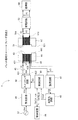
本発明の実施形態の非接触給電装置1について、図1〜図10を参考にして説明する。図1は、本発明の実施形態の非接触給電装置1が組み込まれる部品実装機9の全体構成を示す斜視図である。図1の左奥から右手前に向かう方向が基板Kを搬入出するX軸方向、右奥から左手前に向かう方向がY軸方向、上下に向かう方向がZ軸方向である。部品実装機9は、基板搬送装置92、複数台のフィーダ装置2、パレット部材3、部品移載装置94、部品カメラ95、および制御装置96(図2示)が機台91に組み付けられて構成されている。基板搬送装置92、フィーダ装置2、部品移載装置94、および部品カメラ95は、制御装置96から制御され、それぞれが所定の作業を行うようになっている。
A non-contact
基板搬送装置92は、基板Kを装着実施位置に搬入し位置決めし搬出する。基板搬送装置92は、第1および第2ガイドレール921、922、一対のコンベアベルト、およびクランプ装置などで構成されている。第1および第2ガイドレール921、922は、機台91の上部中央を横断して搬送方向(X軸方向)に延在し、かつ互いに平行するように機台91に組み付けられている。第1および第2ガイドレール921、922の向かい合う内側に、無端環状の一対のコンベアベルト(図略)が並設されている。一対のコンベアベルトは、コンベア搬送面に基板Kの両縁をそれぞれ戴置した状態で輪転して、基板Kを機台91の中央部に設定された装着実施位置に搬入および搬出する。装着実施位置のコンベアベルトの下方には、クランプ装置(図略)が設けられている。クランプ装置は、基板Kを押し上げて水平姿勢でクランプし、装着実施位置に位置決めする。これにより、部品移載装置94が装着実施位置で装着動作を行えるようになる。
The
複数台のフィーダ装置2は、それぞれ電子部品を順次供給する。フィーダ装置2は、上下方向(Z軸方向)および前後方向(Y軸方向)に広がり、幅方向(X軸方向)が薄い扁平形状である。複数台のフィーダ装置2は、パレット部材3の上面の幅方向(X軸方向)に並べて搭載される。各フィーダ装置2は、本体部22と、本体部22の後部に設けられた供給リール23と、本体部22の前端に設けられた部品取出部24とを有している。供給リール23には多数の電子部品が所定ピッチで収納された細長いテープ(図略)が巻回保持されている。このテープが機構部54(図2示)により所定ピッチずつ繰り出され、電子部品が収納状態を解除されて部品取出部24に順次供給されるようになっている。さらに、フィーダ装置2の底面には、パレット部材3への搭載を容易にして位置決めを行うために細長い凸部25(図7示)が形成されている。
The plurality of
パレット部材3は、複数台のフィーダ装置2を搭載するための部材であり、機台91の上面に着脱可能に保持される。パレット部材3は、部品実装機9の本体に属する部材であり、底板部31および前板部32からなる。底板部31は、矩形板状であり、その幅寸法(X軸方向寸法)は、機台91の幅寸法よりも小さめである。前板部32は、底板部31の前縁から立設されている。底板部31の上面には、前後方向(Y軸方向)に延在する溝状のスロット33(図7示)が刻設されている。フィーダ装置2は、底面の凸部25が底板部31のスロット33に挿入された状態で、後方から前板部32に向かってスライド移動されることにより、パレット部材3に搭載される。最終的に、フィーダ装置2は、パレット部材3の底板部31および前板部32に接して搭載される。
The
部品移載装置94は、複数のフィーダ装置2の各部品取出部24から部品を吸着採取し、位置決めされた基板Kまで搬送して装着する。部品移載装置94は、X軸方向およびY軸方向に水平移動可能なXYロボットタイプの装置である。部品移載装置94は、一対のY軸レール941、942、Y軸スライダ943、ヘッド保持部944、および吸着ノズル945などで構成されている。一対のY軸レール941、942は、機台91の前後方向(Y軸方向)に延在して、基板搬送装置92およびフィーダ装置2の上方に配設されている。Y軸レール941、942上に、Y軸スライダ943がY軸方向に移動可能に装架されている。Y軸スライダ943には、ヘッド保持部944がX軸方向に移動可能に装架されている。ヘッド保持部944は、2つのサーボモータによって水平2方向(X軸およびY軸方向)に駆動される。ヘッド保持部944は、その下側に吸着ノズル945を交換可能に保持する。吸着ノズル945は、下端に吸着開口部をもち、負圧を利用して吸着開口部に電子部品を吸着する。
The
部品カメラ95は、基板搬送装置92とフィーダ装置2との間の機台91の上面に、上向きに設けられている。部品カメラ95は、吸着ノズル945がフィーダ装置2から基板K上に移動する途中で、吸着されている電子部品の状態を撮像して検出するものである。部品カメラ95が電子部品の吸着姿勢の誤差や回転角のずれなどを検出すると、制御装置96は、必要に応じて部品装着動作を微調整し、装着が困難な場合には当該の部品を廃棄する。
The
制御装置96は、機台91に設けられている。制御装置96は、基板Kに電子部品を装着する順序および電子部品を供給するフィーダ装置2を指定した装着シーケンスを保持している。制御装置96は、部品カメラ95の撮像データおよび図略のセンサの検出データなどに基づき、装着シーケンスにしたがって部品装着動作を制御する。また、制御装置96は、生産完了した基板Kの生産数や、電子部品の装着に要した装着時間、部品の吸着エラーの発生回数などの稼動データを逐次収集して更新する。
The
次に、実施形態の非接触給電装置1の説明に移る。実施形態の非接触給電装置1は、パレット部材3からフィーダ装置2に向けて、電磁結合方式で非接触給電する装置である。パレット部材3は、本発明の給電側装置、対基板作業機の本体、および部品実装機9の本体に相当する。一方、フィーダ装置2は、本発明の受電側装置、搭載装置、および部品供給装置に相当する。図2は、実施形態の非接触給電装置1の構成を模式的に示す図である。
Next, the description shifts to the contactless
パレット部材3は、非接触給電装置1の構成要素として、図2の左側に示される整流回路41、スイッチング回路42、給電用コイル43、共振用コンデンサ45、補助コイル46、整流回路47、線形化回路48、および制御回路49を有する。一方、フィーダ装置2は、非接触給電装置1の構成要素として、図2の右側に示される受電用コイル51、および受電回路53を有する。また、フィーダ装置2は、給電される電気負荷として、機構部54内にモータおよび制御CPUを有する。
The
パレット部材3側の整流回路41は、交流電源97の商用周波数(50Hzまたは60Hz)の交流電圧Vacを整流して直流電圧Vdcを生成し、スイッチング回路42に供給する。整流回路41として、4個のダイオードをブリッジ接続した全波整流回路を例示でき、これに限定されない。
The
スイッチング回路42は、制御回路49からの駆動信号SDに基づき、直流電圧Vdcをスイッチング制御して高周波電圧Vhfを生成し、出力する。スイッチング回路42の一方の出力端子421は、共振用コンデンサ45を介して給電用コイル43の一端431に接続されている。スイッチング回路42の他方の出力端子422は、給電用コイル43の他端432に直結されている。したがって、高周波電圧Vhfは、共振用コンデンサ45と給電用コイル43との直列回路に印加されることになる。整流回路41およびスイッチング回路42は、本発明の高周波電源回路を構成する。
The switching
給電用コイル43は、給電用コア44に導体が所定回数だけ巻回されて形成されている。給電用コア44は、両端に接合面441を有するC型コアである。これに限定されず、給電用コア44は、センターコアにコイルを巻回するE型コアや、その他の構造のコアであってもよい。給電用コア44を構成する材質として、透磁率の高い電磁鋼板の積層体やフェライトなどを例示でき、透磁率の低いアルミなどであってもよい。給電用コイル43、給電用コア44、および補助コイル46は、パレット部材3の前板部32の上部寄りに配設されている。
The
共振用コンデンサ45は、給電用コイル43に直列接続されて直列共振回路を形成する。給電用コイル43のインダクタンス値および共振用コンデンサ45の静電容量値は、適正に設計されており、所望する共振周波数fsが定まる。共振周波数fsは、スイッチング回路42の出力周波数範囲に含まれている。
The
ここで、周知のように、給電用コイル43および共振用コンデンサ45は、相互に符号の異なる純虚数インピーダンスをもつ。したがって、給電用コイル43の一端431と他端432との間に発生する高周波の一次電圧V1の大きさは、スイッチング回路42の高周波電圧Vhfの大きさを超過することが生じ得る。この現象は、共振周波数fsにおいて給電用コイル43に大きな給電電流I1が流れるときに顕著であり、共振周波数fsの場合だけに限定されない。また、給電用コア44を通る磁束は、磁気飽和しない領域において一次電圧V1および励磁電流の増加にしたがって増加する。
Here, as is well known, the
補助コイル46は、給電用コア44に導体が巻回されて形成され、給電用コイル43に隣接して配置されている。補助コイル46は、導体の断面積が給電用コイル43のそれより小さく、巻回数も給電用コイル43のそれより少ない。換言すると、給電用コイル43に対する補助コイル46の巻数比R3は、1より小さい。補助コイル46の両端で測定される高周波の三次電圧V3は、給電用コア44を通る磁束に比例し、給電用コイル43の一次電圧V1に巻数比R3を乗じた値になる。補助コイル46の両端は、整流回路47に接続されている。
The
整流回路47は、補助コイル46の高周波の三次電圧V3を整流して直流電圧V3dを生成し、線形化回路48に出力する。整流回路47として、整流回路41と同様の全波整流回路を例示でき、これに限定されない。線形化回路48は、或るパラメータに依存して非線形に変化する直流電圧V3dを線形化補正して出力信号Voutを生成し、制御回路49に出力する。或るパラメータとは、後述するように給電用コア44と受電用コア52との電磁結合の結合度、ならびに給電電流I1である。線形化回路48は、例えば、積分回路などを応用して構成できる。
The
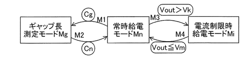
制御回路49は、制御装置96から指令(ギャップ長測定指令Cg、常時給電指令Cn)を受け取るとともに、制御装置96に通知(良好通知Gd、不良通知Ng、電流制限通知Si)を送出する。また、制御回路49は、線形化回路48から受け取った出力信号Voutに対して所定の演算処理を行う。制御回路49は、制御装置96からの指令(ギャップ長測定指令Cg、常時給電指令Cn)および演算処理の結果に基づいて、図3に示される3種類の動作モード(常時給電モードMn、ギャップ長測定モードMg、電流制限時給電モードMi)を遷移する。さらに、制御回路49は、可変の駆動信号SDをスイッチング回路42に出力する。制御回路49の機能については、後の動作の説明で詳述する。
The
フィーダ装置2側の受電用コイル51は、受電用コア52に導体が所定回数だけ巻回されて形成されている。受電用コイル51の導体の断面積および巻回数は、給電用コイル43と同じでもよいし、異なっていてもよい。換言すると、給電用コイル43に対する受電用コイル51の巻数比R2は、1であってもよく、あるいは1より大きくても小さくてもよい。受電用コイル51の一端511および他端512は、受電回路53に接続されている。
The
受電用コア52は、両端に接合面521を有するC型コアである。受電用コア52は、給電用コア44と同じ材質で構成され、かつ同じ形状で概ね等しい磁路断面積を有することが好ましい。受電用コイル51、および受電用コア52は、フィーダ装置2の前面の上部寄りに配設されている。
The
給電用コア44の2個の接合面441と受電用コア52の2個の接合面521とが対向配置されると、閉じた磁気回路が形成される。給電用コア44および受電用コア52は、磁気回路を形成することによって、給電用コイル43と受電用コイル51とを電磁結合する。これにより、受電用コイル51は、給電用コイル43から非接触給電方式で高周波電力を受け取ることができるようになる。そしてこのとき、受電用コイル51から受電回路53に向けて受電電流I2が流れる。また、補助コイル46は、磁気回路の磁路断面積の概ね全体に鎖交する。
When the two
給電用コア44と受電用コア52との電磁結合の結合度に依存して、受電用コイル51の一端511と他端512との間に発生する高周波の二次電圧V2の大きさが変化する。つまり、接合面441、521同士が良好に接合していれば、結合度は概ね1になって、二次電圧V2の大きさは、一次電圧V1に巻数比R2を乗じた値となる。また、接合面441、521同士の接合状態が低下すると、結合度は1から低下して、二次電圧V2の大きさも減少する。
Depending on the degree of electromagnetic coupling between the
受電回路53は、受電用コイル51から受け取った高周波の二次電圧V2を変換して、所定の出力電圧VLを生成し、機構部54の電気負荷に供給する。所定の出力電圧VLとして、一定の直流電圧を例示できる。また、所定の出力電圧VLは、複数種類の電気負荷に対応して大きさの異なる2段階の直流電圧であってもよい。例えば、機構部54内のモータの直流駆動電圧と制御CPUの直流制御電圧とが異なっていても、共に受電回路53から給電される。さらに、受電回路53は、電磁結合の結合度の低下や電気負荷の負荷変動に起因して二次電圧V2や受電電流I2が変動しても、出力電圧VLを一定に保つように動作する。受電回路53は、例えば全波整流回路とレギュレータ(直流定電圧化回路)との組み合わせにより構成できる。
The
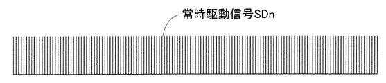
次に、上述のように構成された実施形態の非接触給電装置1の動作について説明する。図3は、制御回路49の動作モードの遷移を説明するモード遷移図である。制御回路49は、常時給電モードMn、ギャップ長測定モードMg、および電流制限時給電モードMiを有する。制御回路49は、各動作モードMn、Mg、Miにおいて互いに異なる駆動信号SDをスイッチング回路42に出力する。図4は、常時給電モードMnにおいて制御回路49がスイッチング回路42に出力する常時駆動信号SDnの波形図である。図5は、ギャップ長測定モードMgにおいて制御回路49がスイッチング回路42に出力する測定時駆動信号SDgの波形図である。図6は、電流制限時給電モードMiにおいて制御回路49がスイッチング回路42に出力する電流制限時駆動信号SDiの波形図である。
Next, operation | movement of the non-contact
常時給電モードMnにおいて制御回路49が出力する図4の常時駆動信号SDnは、共振周波数fsの連続波形である。これにより、スイッチング回路42は、共振周波数fsの高周波電圧Vhfの連続波形を出力する。したがって、常時には、直列共振回路を用いて給電効率の良い非接触給電が行われる。
The constant drive signal SDn of FIG. 4 output by the
ここで、図7に示されるように、フィーダ装置2がパレット部材3に搭載される状況を考える。図7は、フィーダ装置2がパレット部材3に搭載される状況を示す側面図である。フィーダ装置2がパレット部材3に搭載されるときに、受電用コイル51および受電用コア52は、給電用コイル43および給電用コア44に正対する。そして、白抜き矢印Jに示されるようにフィーダ装置2が前方に向かって(図では左方に)スライド移動されると、給電用コア44の接合面441と受電用コア52の接合面521とが正対してギャップ長GLを減少させながら接合または接近する。
Here, as shown in FIG. 7, consider a situation where the
フィーダ装置2が良好に搭載されると、接合面441、521同士が接合して、ギャップ長GLは殆ど無くなる。フィーダ装置2が良好に搭載されない場合には、接合面441、521同士の間に何らかの異常が発生する。例えば、接合面441、521の間にギャップ長GLが残ったままとなり、あるいは、接合面441、521同士が平行せずに片当りし、あるいは、接合面441、521の間に異物を挟み込んでしまい、あるいは、接合面441、521の一部が割れて欠損する。このような異常では、磁気回路に欠陥が発生して、給電用コイル43と受電用コイル51との電磁結合の結合度が低下する。電磁結合の結合度は、ギャップ長GLを最大の変動要因とするが、上述したように他の変動要因も存在する。
When the
上記した異常を監視するために、制御装置96は、フィーダ装置2がパレット部材3に搭載された直後に、ギャップ長測定指令Cgを制御回路49に送出する。ギャップ長測定指令Cgを受け取った制御回路49は、図3の矢印M1に示されるように、常時給電モードMnからギャップ長測定モードMgに遷移する。ギャップ長測定モードMgにおいて、制御回路49は、補助コイル46の測定対象を電磁結合の結合度に設定するとともに、駆動信号SDを測定時駆動信号SDgとする。測定時駆動信号SDgは、図5に示されるように、バースト波形(間欠波形)である。測定時駆動信号SDgでは、共振周波数fsから偏移した周波数で5〜6波形を出力する出力期間T1と、出力しない休止期間T2とが交互に到来する。
In order to monitor the abnormality described above, the
測定時駆動信号SDgを受け取ったスイッチング回路42は、測定時駆動信号SDgに概ね相似した高周波電圧Vhfのバースト波形を出力する。バースト波形に休止期間T2を設けることで、非接触給電する高周波電力を小さくできる。加えて、共振周波数fsから偏移した周波数を用いることで、共振状態が解消されて高周波電力をさらに一層小さくできる。したがって、測定時に装置1を損傷するリスクが格段に低減または解消される。また、制御装置96は、フィーダ装置2が部品供給動作を行わないように禁止制御する。すると、フィーダ装置2の機構部54の電気負荷のうちモータは動作せず、制御CPUのみが動作して概ね一定負荷となり、測定に好適な負荷条件が整う。
The switching
ここで、電磁結合の結合度が変化すると仮定して、補助コイル46で測定される三次電圧V3に着目する。一例として、給電用コア44の接合面441と受電用コア52の接合面521とが良好な接合状態から徐々にギャップ長GLが大きくなって結合度が低下する場合を考える。結合度が低下すると、二次電圧V2は減少するが、一定の電気負荷を駆動する必要上から受電電流I2が増加する。これに伴い、給電電流I1が増加し、一次電圧V1が増加して、三次電圧V3が増加する。つまり、図8に示されるように、ギャップ長GLが大きくなって結合度が低下すると、三次電圧V3は定性的に増加する。図8は、給電用コイル43と受電用コイル51との電磁結合の結合度と、補助コイル46で測定される三次電圧V3との関係を定性的に示す図である。
Here, the third voltage V3 measured by the
ただし、三次電圧V3の波形は、実際には高周波のバースト波形であり、かつ増加の様相は非線形な変化であるため、良否の判定には使用できない。このため、三次電圧V3は、整流回路47により整流され、線形化回路48で線形化補正されて、図9に示される出力信号Voutに変換される。図9は、電磁結合の結合度と、補助コイル46の三次電圧V3が線形化補正された出力信号Voutとの関係を示す図である。図示されるように、出力信号Voutは、電磁結合の結合度の低下(ギャップ長GLの増加)に対して一定の傾きで直線状に増加する。
However, since the waveform of the tertiary voltage V3 is actually a high-frequency burst waveform, and the increase aspect is a non-linear change, it cannot be used to determine pass / fail. Therefore, the tertiary voltage V3 is rectified by the rectifying
制御回路49は、出力信号Voutを受け取り、結合度の良否を判定するための判定値Vjと大小比較する。制御回路49は、出力信号Voutが判定値Vj以下であれば、ギャップ長GLが所定ギャップ長GLj以下で十分な結合度が確保されていると判定する(図9示)。そして、制御回路49は、制御装置96に良好通知Gdを送出する。制御回路49は、出力信号Voutが判定値Vjを超えていれば、十分な結合度が確保されていないと判定して、制御装置96に不良通知Ngを送出する。
The
制御装置96は、良好通知Gdを受け取ると、結合度が良好であると確認できたので、常時給電指令Cnを制御回路49に送出する。これとともに、制御装置96は、フィーダ装置2の部品供給動作を許可制御する。常時給電指令Cnを受け取った制御回路49は、図3の矢印M2に示されるように、ギャップ長測定モードMgから常時給電モードMnに遷移する。また、制御装置96は、不良通知Ngを受け取ると、その旨をオペレータに報知してオペレータの対応を待つ。上述した説明で分かるように、制御回路49は、本発明の測定対象制御回路ならびに本発明の電圧制御回路として動作する。
When the
次に、常時給電モードMnにおいて、制御回路49は、補助コイル46の測定対象を給電電流I1の大きさに設定するするとともに、駆動信号SDを図4の常時駆動信号SDnとする。常時給電モードMnにおいて、電磁結合の結合度は著変せず、部品供給動作により機構部54のモータが負荷変動する。このとき、電気負荷が増加しても二次電圧V2は変化せず、電気負荷の増加分に対応して受電電流I2が増加する。これに伴い、給電電流I1が増加し、一次電圧V1が増加して、三次電圧V3が増加する。つまり、受電側の電気負荷の増加により給電側の給電電流I1が増加すると、三次電圧V3は定性的に増加する。
Next, in the constant power supply mode Mn, the
この三次電圧V3は、ギャップ長測定モードMgと同様に、整流回路47により整流され、線形化回路48で線形化補正されて、図10に示される出力信号Voutに変換される。図10は、給電電流I1の大きさと、補助コイル46の三次電圧V3が線形化補正された出力信号Voutとの関係を示す図である。図示されるように、出力信号Voutは、給電電流I1の増加に対して一定の傾きで直線状に増加する。
Similar to the gap length measurement mode Mg, this tertiary voltage V3 is rectified by the
制御回路49は、出力信号Voutを受け取り、ギャップ長測定モードMgのときと異なる所定の判定値Vkと大小比較して、モード遷移の要否を判定する。制御回路49は、出力信号Voutが判定値Vk以下であれば、常時給電モードMnを維持する。制御回路49は、出力信号Voutが判定値Vkを超えていると、給電電流I1の大きさが過大であり、過電流による装置1の損傷のリスクが生じ、あるいはリスクが高まったと判定する。そして、制御回路49は、図3の矢印M3に示されるように、電流制限時給電モードMiに遷移する。
The
電流制限時給電モードMiにおいて、制御回路49は、駆動信号SDを電流制限時駆動信号SDiとし、補助コイル46による給電電流I1の測定を継続する。また、制御回路49は、電流制限時給電モードMiで動作している旨の電流制限通知Siを制御装置96に送出する。電流制限時駆動信号SDiは、図6に示されるように、共振周波数fsの連続波形が或る頻度で間引かれて生成されたバースト波形(間欠波形)である。図6に示される例では、連続する3波形W1〜W3が残されてその後の1波形W4が間引かれたバースト波形(間欠波形)が繰り返されている。電流制限時駆動信号SDiを受け取ったスイッチング回路42は、電流制限時駆動信号SDiに概ね相似した高周波電圧Vhfのバースト波形を出力する。このバースト波形では、給電電流I1の実効値が制限されるので、過電流により装置1を損傷するリスクが低減または解消される。
In the current limiting power supply mode Mi, the
制御回路49は、給電電流I1の測定を継続し、出力信号Voutをさらに別の判定値Vmと大小比較する。制御回路49は、出力信号Voutが判定値Vmを超えていると電流制限時給電モードMiを維持する。そして、出力信号Voutが判定値Vm以下に減少すると、制御回路49は、電流制限の必要が無くなったと判定し、図3の矢印M4に示されるように、常時給電モードMnに遷移する。上述した説明で分かるように、制御回路49は、本発明の測定対象制御回路ならびに本発明の電流制御回路として動作する。
The
実施形態の非接触給電装置1は、パレット部材3に設けられた給電用コイル43と、給電用コイル43に高周波電圧Vhfを印加するスイッチング回路42(高周波電源回路)と、パレット部材3に対向配置されるフィーダ装置2に設けられ給電用コイル43と電磁結合して非接触給電により高周波電力を受け取る受電用コイル51と、受電用コイル51が受け取った高周波電力を変換してフィーダ装置2の電気負荷に給電する受電回路53と、パレット部材3に設けられて、給電用コイル43と受電用コイル51とを電磁結合させる磁気回路の少なくとも一部に鎖交する補助コイル46と、を備えた。
The contactless
これによれば、非接触給電の回路を構成する磁気回路に補助コイル46を鎖交させて組み入れることができる。そして、補助コイル46により、給電用コイル43と受電用コイル51との電磁結合の結合度、ならびに、給電用コイル43に流れる給電電流I1の大きさの少なくとも一方を測定することができる。したがって、簡素な構成でありながら付加機能を有する高性能な非接触給電装置1を実現できる。
According to this, the
さらに、実施形態の非接触給電装置1において、補助コイル46は、給電用コイル43と受電用コイル51との電磁結合の結合度を測定するものである。加えて、補助コイル46が電磁結合の結合度を測定する測定時に、高周波電圧Vhfの連続波形とバースト波形との切り替えを制御して、非接触給電する高周波電力を小さくする制御回路49(電圧制御回路)をさらに備えた。
Furthermore, in the non-contact
これによれば、バースト波形に休止期間T2を設けることで非接触給電する高周波電力を小さくできる。したがって、測定時に装置1を損傷するリスクが低減される。
According to this, it is possible to reduce the high frequency power to be contactlessly fed by providing the pause waveform with the pause period T2. Therefore, the risk of damaging the
さらに、実施形態の非接触給電装置1は、給電用コイル43に直列接続されて直列共振回路を形成する共振用コンデンサ45をさらに備え、制御回路49は、補助コイル46が電磁結合の結合度を測定しない常時には高周波電圧Vhfの周波数を共振周波数fsに維持し、測定時には高周波電圧Vhfの周波数を共振周波数fsから偏移させる。
Furthermore, the contactless
これによれば、常時には、直列共振回路を用いて給電効率の良い非接触給電が行われる。また、測定時には、共振状態が解消されるので、非接触給電する高周波電力をさらに一層小さくできる。したがって、測定時に装置1を損傷するリスクが格段に低減または解消される。
According to this, contactless power feeding with good power feeding efficiency is always performed using a series resonance circuit. Further, at the time of measurement, since the resonance state is eliminated, the high frequency power to be contactlessly fed can be further reduced. Therefore, the risk of damaging the
また、実施形態の非接触給電装置1において、補助コイル46は、高周波電圧Vhfによって給電用コイル43に流れる給電電流I1の大きさを測定するものである。加えて、補助コイル46によって測定された給電電流I1の大きさが過大であるときに、高周波電圧の連続波形とバースト波形との切り替えを制御して給電電流I1を制限する制御回路49(電流制御回路)をさらに備えた。
Moreover, in the non-contact
これによれば、連続波形が或る頻度で間引かれて生成されたバースト波形によって給電電流I1の実効値が制限されるので、過電流により装置1を損傷するリスクが低減または解消される。
According to this, since the effective value of the feeding current I1 is limited by the burst waveform generated by thinning out the continuous waveform at a certain frequency, the risk of damaging the
さらに、実施形態の非接触給電装置1において、補助コイル46は、給電用コイル43と受電用コイルと51の電磁結合の結合度、ならびに、高周波電圧Vhfによって給電用コイル43に流れる給電電流I1の大きさを切り替えて測定するものであり、補助コイル46の測定対象を電磁結合の結合度および給電電流I1の大きさに切り替え設定するとともに、補助コイル46の測定対象に適合するように高周波電圧Vhfを可変に制御する制御回路49(測定対象制御回路)をさらに備えた。
Furthermore, in the non-contact
これによれば、補助コイル46を用いることにより、給電用コイル43と受電用コイル51との電磁結合の結合度、ならびに、給電用コイル43に流れる給電電流I1の大きさの両方を切り替えて測定することができる。したがって、簡素な構成でありながら2種類の付加機能を有してさらに一層高性能な非接触給電装置1を実現できる。
According to this, by using the
さらに、実施形態の非接触給電装置1において、制御回路49は、パレット部材3にフィーダ装置2が対向配置された直後に、補助コイル46の測定対象を電磁結合の結合度に設定し、電磁結合の結合度が良好であると確認されると、補助コイル46の測定対象を給電電流I1の大きさに切り替え設定する。
Furthermore, in the non-contact
これによれば、フィーダ装置2をパレット部材3へ搭載した直後に搭載状況の良否を確認できるので、搭載状況が低下しているフィーダ装置2が無理に使用されない。また、搭載状況が良好であると確認されると、フィーダ装置2の部品供給動作が許可制御され、引き続いて給電電流I1の測定にスムーズに移行できる。
According to this, immediately after the
さらに、実施形態の非接触給電装置1において、部品実装機9のパレット部材3に設けられた給電用コイル43は、電磁結合を担うとともに補助コイル46が巻回された給電用コア44を有し、フィーダ装置2に設けられた受電用コイル51は、給電用コア44と共同して電磁結合を担う受電用コア52を有し、フィーダ装置2がパレット部材3に搭載されるときに、給電用コア44の接合面441と受電用コア52の接合面521とが正対してギャップ長GLを減少させながら接合または接近する。
Furthermore, in the non-contact
これによれば、フィーダ装置2をパレット部材3に搭載するときに、フィーダ装置2が十分にスライド移動されずに大きなギャップ長GLが残された搭載状況を確実に異常と判定できる。
According to this, when the
なお、実施形態において、ギャップ長測定モードMgで用いる測定時駆動信号SDgは、図5のバースト波形に限定されない。例えば、共振周波数fsから偏移した周波数の連続波形であってもよい。また例えば、共振周波数fsの連続波形を用いつつ、直流電圧Vdcを低減制御するようにしてもよい。上記した2例の別波形でも、測定時に装置1を損傷するリスクは低減される。また、電流制限時給電モードMiにおいて給電電流I1の実効値を制限する方法は、図6に示されるバースト波形(間欠波形)以外にもある。例えば、共振周波数fsの連続波形を用いつつ、直流電圧Vdcを低減制御してもよい。
In the embodiment, the measurement drive signal SDg used in the gap length measurement mode Mg is not limited to the burst waveform of FIG. For example, a continuous waveform having a frequency shifted from the resonance frequency fs may be used. Further, for example, the DC voltage Vdc may be controlled to be reduced while using a continuous waveform of the resonance frequency fs. The risk of damaging the
さらになお、共振用コンデンサ45の個数や接続方法も変更でき、例えば、フィーダ装置2側の受電用コイル51にコンデンサを並列接続して追加してもよい。また、実施形態で説明した以外の判定値を制御回路49に設定して、補助コイル46を用いた測定結果と比較することで、多様な判定や複雑な制御が可能となる。例えば、出力信号Voutの時間変化率から非接触給電回路の故障を監視したり、出力信号Voutの時間的な上昇パターンからフィーダ装置2の着脱操作が行われたことを判定したりできる。本発明は、その他にも様々な応用や変形が可能である。
Furthermore, the number and connection method of the
本発明の非接触給電装置は、実施形態で説明した部品実装機9のフィーダ装置2以外にも、他種の対基板作業機や、他の製品を生産する組立機や加工機などに幅広く利用できる。
The contactless power supply device of the present invention is widely used for other types of substrate work machines, assembly machines and processing machines for producing other products, in addition to the
1:非接触給電装置
2:フィーダ装置(受電側装置、搭載装置)
3:パレット部材(給電側装置、対基板作業機の本体)
41:整流回路 42:スイッチング回路 43:給電用コイル
44:給電用コア 441:接合面 45:共振用コンデンサ
46:補助コイル 47:整流回路 48:線形化回路
49:制御回路(電圧制御回路、電流制御回路、測定対象制御回路)
51:受電用コイル 52:受電用コア 521:接合面
53:受電回路 54:機構部(電気負荷)
9:部品実装機 91:機台 92:基板搬送装置
94:部品移載装置 95:部品カメラ 96:制御装置
Vhf:高周波電圧 SD:駆動信号 Vout:出力信号
V1:一次電圧 V2:二次電圧 V3:三次電圧
I1:給電電流 I2:受電電流 GL:ギャップ長1: Non-contact power feeding device 2: Feeder device (power receiving side device, mounting device)
3: Pallet member (power supply side device, main body of substrate work machine)
41: Rectifier circuit 42: Switching circuit 43: Power supply coil 44: Power supply core 441: Bonding surface 45: Resonance capacitor 46: Auxiliary coil 47: Rectifier circuit 48: Linearization circuit 49: Control circuit (voltage control circuit, current Control circuit, measurement target control circuit)
51: Coil for power reception 52: Core for power reception 521: Bonding surface 53: Power reception circuit 54: Mechanism (electric load)
9: Component mounter 91: Machine base 92: Board transfer device 94: Component transfer device 95: Component camera 96: Control device Vhf: High frequency voltage SD: Drive signal Vout: Output signal V1: Primary voltage V2: Secondary voltage V3 : Tertiary voltage I1: Feeding current I2: Receiving current GL: Gap length
Claims (10)
前記給電用コイルに高周波電圧を印加する高周波電源回路と、
前記給電側装置に対向配置される受電側装置に設けられ、前記給電用コイルと電磁結合して非接触給電により高周波電力を受け取る受電用コイルと、
前記受電用コイルが受け取った高周波電力を変換して前記受電側装置の電気負荷に給電する受電回路と、
前記給電側装置に設けられて、前記給電用コイルと前記受電用コイルとを電磁結合させる磁気回路の少なくとも一部に鎖交する補助コイルと、を備え、
前記補助コイルは、前記給電用コイルと前記受電用コイルとの電磁結合の結合度を測定するものであり、
前記補助コイルが前記電磁結合の結合度を測定する測定時に、前記高周波電圧の周波数、電圧値、および連続波形とバースト波形との切り替えの少なくともひとつを制御して、非接触給電する高周波電力を小さくする電圧制御回路をさらに備えた、
非接触給電装置。 A power supply coil provided in the power supply side device;
A high frequency power supply circuit for applying a high frequency voltage to the power supply coil;
A power receiving coil provided in a power receiving side device disposed opposite to the power feeding side device, and electromagnetically coupled to the power feeding coil to receive high frequency power by non-contact power feeding;
A power receiving circuit that converts the high frequency power received by the power receiving coil and supplies power to the electric load of the power receiving side device;
An auxiliary coil provided in the power supply side device and interlinked with at least a part of a magnetic circuit that electromagnetically couples the power supply coil and the power reception coil ;
The auxiliary coil measures the degree of electromagnetic coupling between the power feeding coil and the power receiving coil,
When measuring the degree of electromagnetic coupling, the auxiliary coil controls the frequency of the high-frequency voltage, the voltage value, and at least one of switching between a continuous waveform and a burst waveform to reduce the high-frequency power to be contactlessly fed. A voltage control circuit for
Non-contact power feeding device.
前記電圧制御回路は、前記補助コイルが前記電磁結合の結合度を測定しない常時には前記高周波電圧の周波数を共振周波数に維持し、前記測定時には前記高周波電圧の周波数を前記共振周波数から偏移させる請求項1に記載の非接触給電装置。 A resonance capacitor connected to at least one of the power feeding coil and the power receiving coil to form a resonance circuit;
Wherein said voltage control circuit, constantly to the auxiliary coil does not measure the degree of coupling of the electromagnetic coupling will maintain the frequency of the high frequency voltage to the resonance frequency, said during measurement to shift the frequency of the high frequency voltage from the resonant frequency Item 2. The non-contact power feeding device according to Item 1 .
前記給電用コイルに高周波電圧を印加する高周波電源回路と、
前記給電側装置に対向配置される受電側装置に設けられ、前記給電用コイルと電磁結合して非接触給電により高周波電力を受け取る受電用コイルと、
前記受電用コイルが受け取った高周波電力を変換して前記受電側装置の電気負荷に給電する受電回路と、
前記給電側装置に設けられて、前記給電用コイルと前記受電用コイルとを電磁結合させる磁気回路の少なくとも一部に鎖交する補助コイルと、を備え、
前記補助コイルは、前記高周波電圧によって前記給電用コイルに流れる給電電流の大きさを測定するものである非接触給電装置。 A power supply coil provided in the power supply side device;
A high frequency power supply circuit for applying a high frequency voltage to the power supply coil;
A power receiving coil provided in a power receiving side device disposed opposite to the power feeding side device, and electromagnetically coupled to the power feeding coil to receive high frequency power by non-contact power feeding;
A power receiving circuit that converts the high frequency power received by the power receiving coil and supplies power to the electric load of the power receiving side device;
An auxiliary coil provided in the power supply side device and interlinked with at least a part of a magnetic circuit that electromagnetically couples the power supply coil and the power reception coil;
The auxiliary coil, der Ru contactless power supply apparatus measures the magnitude of the supply current flowing through the power supply coil by the high frequency voltage.
前記給電用コイルに高周波電圧を印加する高周波電源回路と、
前記給電側装置に対向配置される受電側装置に設けられ、前記給電用コイルと電磁結合して非接触給電により高周波電力を受け取る受電用コイルと、
前記受電用コイルが受け取った高周波電力を変換して前記受電側装置の電気負荷に給電する受電回路と、
前記給電側装置に設けられて、前記給電用コイルと前記受電用コイルとを電磁結合させる磁気回路の少なくとも一部に鎖交する補助コイルと、を備え、
前記補助コイルは、前記給電用コイルと前記受電用コイルとの電磁結合の結合度、ならびに、前記高周波電圧によって前記給電用コイルに流れる給電電流の大きさを切り替えて測定するものであり、
前記補助コイルの測定対象を前記電磁結合の結合度および前記給電電流の大きさに切り替え設定するとともに、前記補助コイルの測定対象に適合するように前記高周波電圧を可変に制御する測定対象制御回路をさらに備えた非接触給電装置。 A power supply coil provided in the power supply side device;
A high frequency power supply circuit for applying a high frequency voltage to the power supply coil;
A power receiving coil provided in a power receiving side device disposed opposite to the power feeding side device, and electromagnetically coupled to the power feeding coil to receive high frequency power by non-contact power feeding;
A power receiving circuit that converts the high frequency power received by the power receiving coil and supplies power to the electric load of the power receiving side device;
An auxiliary coil provided in the power supply side device and interlinked with at least a part of a magnetic circuit that electromagnetically couples the power supply coil and the power reception coil;
The auxiliary coil measures the degree of coupling of electromagnetic coupling between the power feeding coil and the power receiving coil, and the magnitude of the power feeding current flowing through the power feeding coil by the high frequency voltage.
A measurement target control circuit that switches and sets the measurement target of the auxiliary coil to the coupling degree of the electromagnetic coupling and the magnitude of the feeding current, and variably controls the high-frequency voltage so as to match the measurement target of the auxiliary coil Furthermore, the non- contact electric power feeder provided.
前記補助コイルの測定対象を前記電磁結合の結合度および前記給電電流の大きさに切り替え設定するとともに、前記補助コイルの測定対象に適合するように前記高周波電圧を可変に制御する測定対象制御回路をさらに備えた請求項1〜5のいずれか一項に記載の非接触給電装置。 The auxiliary coil measures the degree of coupling of electromagnetic coupling between the power feeding coil and the power receiving coil, and the magnitude of the power feeding current flowing through the power feeding coil by the high frequency voltage.
A measurement target control circuit that switches and sets the measurement target of the auxiliary coil to the coupling degree of the electromagnetic coupling and the magnitude of the feeding current, and variably controls the high-frequency voltage so as to match the measurement target of the auxiliary coil Furthermore, the non-contact electric power feeder as described in any one of Claims 1-5 provided.
前記給電側装置に前記給電側装置が対向配置された直後に、前記補助コイルの測定対象を前記電磁結合の結合度に設定し、
前記電磁結合の結合度が良好であると確認されると、前記補助コイルの測定対象を前記給電電流の大きさに切り替え設定する請求項6または7に記載の非接触給電装置。 The measurement object control circuit includes:
Immediately after the power feeding side device is disposed opposite to the power feeding side device, the measurement target of the auxiliary coil is set to the degree of coupling of the electromagnetic coupling,
The contactless power feeding device according to claim 6 or 7 , wherein when the degree of coupling of the electromagnetic coupling is confirmed to be good, the measurement target of the auxiliary coil is switched to the magnitude of the feeding current.
前記部品実装機の本体に設けられた前記給電用コイルは、前記電磁結合を担うとともに前記補助コイルが巻回された給電用コアを有し、
前記部品供給装置に設けられた前記受電用コイルは、前記給電用コアと共同して前記電磁結合を担う受電用コアを有し、
前記部品供給装置が前記部品実装機の本体に搭載されるときに、前記給電用コアの接合面と前記受電用コアの接合面とが正対してギャップ長を減少させながら接合または接近する請求項9に記載の非接触給電装置。 The main body of the substrate working machine is a main body of a component mounting machine that mounts electronic components on the board, and the mounting device is detachably mounted on the component mounting machine and supplies the electronic components. And
Wherein the power supply coil provided in the main body of the component mounting apparatus has a feeding core the auxiliary coil is wound with responsible said electromagnetic coupling,
Wherein said power receiving coil provided in the component supply device includes a power receiving core responsible for the electromagnetic coupling in cooperation with the feeding core,
The joint surface of the power feeding core and the joint surface of the power receiving core are opposed to each other while the gap length is reduced when the component supply device is mounted on a main body of the component mounter. The non-contact power feeding device according to 9.
Applications Claiming Priority (1)
| Application Number | Priority Date | Filing Date | Title |
|---|---|---|---|
| PCT/JP2014/068955 WO2016009513A1 (en) | 2014-07-16 | 2014-07-16 | Wireless power supply device |
Publications (2)
| Publication Number | Publication Date |
|---|---|
| JPWO2016009513A1 JPWO2016009513A1 (en) | 2017-04-27 |
| JP6343003B2 true JP6343003B2 (en) | 2018-06-13 |
Family
ID=55078032
Family Applications (1)
| Application Number | Title | Priority Date | Filing Date |
|---|---|---|---|
| JP2016534032A Active JP6343003B2 (en) | 2014-07-16 | 2014-07-16 | Non-contact power feeding device |
Country Status (3)
| Country | Link |
|---|---|
| US (1) | US10305326B2 (en) |
| JP (1) | JP6343003B2 (en) |
| WO (1) | WO2016009513A1 (en) |
Families Citing this family (3)
| Publication number | Priority date | Publication date | Assignee | Title |
|---|---|---|---|---|
| US10602840B2 (en) | 2015-10-08 | 2020-03-31 | Ergotron, Inc. | Height adjustable table |
| US20170353056A1 (en) * | 2016-06-02 | 2017-12-07 | Panasonic Corporation | Electromagnetic resonant coupler including input line, first resonance line, second resonance line, output line, and coupling line, and transmission apparatus including the electromagnetic resonant coupler |
| WO2018020890A1 (en) * | 2016-07-29 | 2018-02-01 | ソニーセミコンダクタソリューションズ株式会社 | Power-supplying system |
Family Cites Families (16)
| Publication number | Priority date | Publication date | Assignee | Title |
|---|---|---|---|---|
| JP2754434B2 (en) * | 1992-04-07 | 1998-05-20 | 本田技研工業株式会社 | Engine ignition device |
| JP3752731B2 (en) * | 1996-05-15 | 2006-03-08 | ソニー株式会社 | Component mounting device |
| JP4631083B2 (en) | 2004-03-12 | 2011-02-16 | 学校法人東京理科大学 | Medical device having implantable drive unit and abnormality detection method thereof |
| US7351181B2 (en) * | 2004-06-28 | 2008-04-01 | Robert Smith | Continuously variable transmission |
| GB2421595A (en) * | 2004-12-21 | 2006-06-28 | Cambridge Semiconductor Ltd | Switched mode power supply control system |
| JP4557792B2 (en) | 2005-05-16 | 2010-10-06 | 株式会社東京精密 | Distance measuring device and machine tool |
| US7989986B2 (en) * | 2006-03-23 | 2011-08-02 | Access Business Group International Llc | Inductive power supply with device identification |
| GB0710057D0 (en) * | 2007-05-25 | 2007-07-04 | Splashpower | Power system |
| US8127477B2 (en) * | 2008-05-13 | 2012-03-06 | Nthdegree Technologies Worldwide Inc | Illuminating display systems |
| US8751001B2 (en) * | 2008-10-23 | 2014-06-10 | Medtronic, Inc. | Universal recharging of an implantable medical device |
| JP5289197B2 (en) | 2009-06-08 | 2013-09-11 | Juki株式会社 | Electronic component mounting equipment |
| JP2011078266A (en) | 2009-10-01 | 2011-04-14 | Sharp Corp | Noncontact power supply equipment |
| US9058928B2 (en) * | 2010-12-14 | 2015-06-16 | Tdk Corporation | Wireless power feeder and wireless power transmission system |
| JP5909700B2 (en) * | 2012-03-09 | 2016-04-27 | パナソニックIpマネジメント株式会社 | Metal detection method, metal detection device, and metal detection method and non-contact power supply device of non-contact power supply device |
| JP5546710B2 (en) * | 2012-04-27 | 2014-07-09 | 三菱電機株式会社 | DC / DC converter, in-vehicle device and charging device |
| CN105594098B (en) * | 2014-02-28 | 2020-01-21 | 松下知识产权经营株式会社 | Foreign object detection device, power transmission device and power reception device for wireless power transmission, and wireless power transmission system |
-
2014
- 2014-07-16 WO PCT/JP2014/068955 patent/WO2016009513A1/en active Application Filing
- 2014-07-16 US US15/324,907 patent/US10305326B2/en active Active
- 2014-07-16 JP JP2016534032A patent/JP6343003B2/en active Active
Also Published As
| Publication number | Publication date |
|---|---|
| WO2016009513A1 (en) | 2016-01-21 |
| US20170201124A1 (en) | 2017-07-13 |
| US10305326B2 (en) | 2019-05-28 |
| JPWO2016009513A1 (en) | 2017-04-27 |
Similar Documents
| Publication | Publication Date | Title |
|---|---|---|
| JP6706623B2 (en) | Contactless power supply system | |
| JP6343003B2 (en) | Non-contact power feeding device | |
| US9831720B2 (en) | Electrostatic-coupling contactless power supply device | |
| JP6076355B2 (en) | Non-contact power feeding device | |
| JP6170057B2 (en) | Electrostatic coupling type non-contact power feeding device and control method thereof | |
| JP6353046B2 (en) | Power supply device | |
| US10355495B2 (en) | Non-contact power feeding device | |
| JP6086927B2 (en) | Electrostatic coupling type non-contact power supply device | |
| JP5976821B2 (en) | Chip mounter and equipment | |
| JP6441929B2 (en) | Non-contact power feeding device | |
| JP2009182117A (en) | Component supply device and mounting device | |
| US11422281B2 (en) | Foreign matter detecting device | |
| EP2903132B1 (en) | Capacitive-coupling-system non-contacting power-feed apparatus | |
| JP6678730B2 (en) | Wireless power supply | |
| JP2017147848A (en) | Non-contact power supply device | |
| JP2009182116A (en) | Component supply device and its power supply method, and mounting device |
Legal Events
| Date | Code | Title | Description |
|---|---|---|---|
| A621 | Written request for application examination |
Free format text: JAPANESE INTERMEDIATE CODE: A621 Effective date: 20170605 |
|
| A131 | Notification of reasons for refusal |
Free format text: JAPANESE INTERMEDIATE CODE: A131 Effective date: 20180206 |
|
| A521 | Request for written amendment filed |
Free format text: JAPANESE INTERMEDIATE CODE: A523 Effective date: 20180330 |
|
| TRDD | Decision of grant or rejection written | ||
| A01 | Written decision to grant a patent or to grant a registration (utility model) |
Free format text: JAPANESE INTERMEDIATE CODE: A01 Effective date: 20180424 |
|
| A61 | First payment of annual fees (during grant procedure) |
Free format text: JAPANESE INTERMEDIATE CODE: A61 Effective date: 20180517 |
|
| R150 | Certificate of patent or registration of utility model |
Ref document number: 6343003 Country of ref document: JP Free format text: JAPANESE INTERMEDIATE CODE: R150 |
|
| R250 | Receipt of annual fees |
Free format text: JAPANESE INTERMEDIATE CODE: R250 |
|
| R250 | Receipt of annual fees |
Free format text: JAPANESE INTERMEDIATE CODE: R250 |
|
| R250 | Receipt of annual fees |
Free format text: JAPANESE INTERMEDIATE CODE: R250 |
|
| R250 | Receipt of annual fees |
Free format text: JAPANESE INTERMEDIATE CODE: R250 |