JP6339697B2 - Cache memory error detection circuit for detecting a bit flip in a valid indicator in a cache memory after an invalidation operation, and related method and processor-based system - Google Patents
Cache memory error detection circuit for detecting a bit flip in a valid indicator in a cache memory after an invalidation operation, and related method and processor-based system Download PDFInfo
- Publication number
- JP6339697B2 JP6339697B2 JP2016562524A JP2016562524A JP6339697B2 JP 6339697 B2 JP6339697 B2 JP 6339697B2 JP 2016562524 A JP2016562524 A JP 2016562524A JP 2016562524 A JP2016562524 A JP 2016562524A JP 6339697 B2 JP6339697 B2 JP 6339697B2
- Authority
- JP
- Japan
- Prior art keywords
- indicator
- cache
- invalidation
- cache memory
- information indicator
- Prior art date
- Legal status (The legal status is an assumption and is not a legal conclusion. Google has not performed a legal analysis and makes no representation as to the accuracy of the status listed.)
- Expired - Fee Related
Links
Images


Classifications
-
- G—PHYSICS
- G06—COMPUTING; CALCULATING OR COUNTING
- G06F—ELECTRIC DIGITAL DATA PROCESSING
- G06F11/00—Error detection; Error correction; Monitoring
- G06F11/07—Responding to the occurrence of a fault, e.g. fault tolerance
- G06F11/08—Error detection or correction by redundancy in data representation, e.g. by using checking codes
- G06F11/10—Adding special bits or symbols to the coded information, e.g. parity check, casting out 9's or 11's
- G06F11/1004—Adding special bits or symbols to the coded information, e.g. parity check, casting out 9's or 11's to protect a block of data words, e.g. CRC or checksum
-
- G—PHYSICS
- G06—COMPUTING; CALCULATING OR COUNTING
- G06F—ELECTRIC DIGITAL DATA PROCESSING
- G06F11/00—Error detection; Error correction; Monitoring
- G06F11/07—Responding to the occurrence of a fault, e.g. fault tolerance
- G06F11/08—Error detection or correction by redundancy in data representation, e.g. by using checking codes
- G06F11/10—Adding special bits or symbols to the coded information, e.g. parity check, casting out 9's or 11's
- G06F11/1008—Adding special bits or symbols to the coded information, e.g. parity check, casting out 9's or 11's in individual solid state devices
- G06F11/1064—Adding special bits or symbols to the coded information, e.g. parity check, casting out 9's or 11's in individual solid state devices in cache or content addressable memories
-
- G—PHYSICS
- G06—COMPUTING; CALCULATING OR COUNTING
- G06F—ELECTRIC DIGITAL DATA PROCESSING
- G06F12/00—Accessing, addressing or allocating within memory systems or architectures
- G06F12/02—Addressing or allocation; Relocation
- G06F12/08—Addressing or allocation; Relocation in hierarchically structured memory systems, e.g. virtual memory systems
- G06F12/0802—Addressing of a memory level in which the access to the desired data or data block requires associative addressing means, e.g. caches
- G06F12/0891—Addressing of a memory level in which the access to the desired data or data block requires associative addressing means, e.g. caches using clearing, invalidating or resetting means
-
- G—PHYSICS
- G06—COMPUTING; CALCULATING OR COUNTING
- G06F—ELECTRIC DIGITAL DATA PROCESSING
- G06F3/00—Input arrangements for transferring data to be processed into a form capable of being handled by the computer; Output arrangements for transferring data from processing unit to output unit, e.g. interface arrangements
- G06F3/06—Digital input from, or digital output to, record carriers, e.g. RAID, emulated record carriers or networked record carriers
- G06F3/0601—Interfaces specially adapted for storage systems
- G06F3/0602—Interfaces specially adapted for storage systems specifically adapted to achieve a particular effect
- G06F3/0614—Improving the reliability of storage systems
- G06F3/0619—Improving the reliability of storage systems in relation to data integrity, e.g. data losses, bit errors
-
- G—PHYSICS
- G06—COMPUTING; CALCULATING OR COUNTING
- G06F—ELECTRIC DIGITAL DATA PROCESSING
- G06F3/00—Input arrangements for transferring data to be processed into a form capable of being handled by the computer; Output arrangements for transferring data from processing unit to output unit, e.g. interface arrangements
- G06F3/06—Digital input from, or digital output to, record carriers, e.g. RAID, emulated record carriers or networked record carriers
- G06F3/0601—Interfaces specially adapted for storage systems
- G06F3/0628—Interfaces specially adapted for storage systems making use of a particular technique
- G06F3/0638—Organizing or formatting or addressing of data
-
- G—PHYSICS
- G06—COMPUTING; CALCULATING OR COUNTING
- G06F—ELECTRIC DIGITAL DATA PROCESSING
- G06F3/00—Input arrangements for transferring data to be processed into a form capable of being handled by the computer; Output arrangements for transferring data from processing unit to output unit, e.g. interface arrangements
- G06F3/06—Digital input from, or digital output to, record carriers, e.g. RAID, emulated record carriers or networked record carriers
- G06F3/0601—Interfaces specially adapted for storage systems
- G06F3/0668—Interfaces specially adapted for storage systems adopting a particular infrastructure
- G06F3/0671—In-line storage system
- G06F3/0673—Single storage device
- G06F3/0674—Disk device
Landscapes
- Engineering & Computer Science (AREA)
- Theoretical Computer Science (AREA)
- General Engineering & Computer Science (AREA)
- Physics & Mathematics (AREA)
- General Physics & Mathematics (AREA)
- Human Computer Interaction (AREA)
- Quality & Reliability (AREA)
- Computer Security & Cryptography (AREA)
- Memory System Of A Hierarchy Structure (AREA)
- Techniques For Improving Reliability Of Storages (AREA)
- Detection And Correction Of Errors (AREA)
Description
優先権主張
本出願は、その全体が参照により本明細書に組み込まれる、2014年4月18日に出願された「CACHE MEMORY ERROR DETECTION CIRCUITS FOR DETECTING BIT FLIPS IN VALID INDICATORS IN CACHE MEMORY FOLLOWING INVALIDATE OPERATIONS, AND RELATED METHODS AND PROCESSOR-BASED SYSTEMS」という名称の米国特許出願第14/256,360号の優先権を主張する。
Priority claim Claims priority of US patent application Ser. No. 14 / 256,360 entitled “RELATED METHODS AND PROCESSOR-BASED SYSTEMS”.
本開示の分野は、プロセッサベースのシステム内のキャッシュメモリにおけるビットフリップを検出することに関する。 The field of this disclosure relates to detecting bit flips in cache memory in processor-based systems.
メモリセルは、「メモリ」としても知られるコンピュータデータストレージの基本ビルディングブロックである。コンピュータシステムは、メモリからデータを読み込むかまたはデータをメモリに書き込むことができる。メモリは、一例として、中央処理装置(CPU)システムにおいてキャッシュメモリを提供するために使用され得る。キャッシュメモリは、メモリアクセスレイテンシを低減するために、メインメモリまたは上位レベルキャッシュメモリ内の頻繁にアクセスされるメモリアドレスにおいて記憶されたデータのコピーを記憶する、より小型でより高速なメモリである。したがって、キャッシュメモリは、メモリアクセス時間を低減するためにCPUによって使用され得るメモリである。 A memory cell is the basic building block of computer data storage, also known as “memory”. The computer system can read data from memory or write data to memory. The memory may be used to provide cache memory, for example, in a central processing unit (CPU) system. Cache memory is a smaller and faster memory that stores a copy of data stored at frequently accessed memory addresses in main memory or higher level cache memory to reduce memory access latency. Thus, cache memory is memory that can be used by the CPU to reduce memory access time.
キャッシュメモリは、タグアレイおよびデータアレイから成る。タグアレイは、「タグ」としても知られるアドレスを含む。タグは、データアレイ内のデータ記憶ロケーションへのインデックスを提供する。タグアレイ内のタグおよびデータアレイ内のタグのインデックスにおいて記憶されたデータは、「キャッシュライン」または「キャッシュエントリ」としても知られる。メモリアクセス要求の一部としてキャッシュメモリに提供されるメモリアドレスまたはその部分がタグアレイ内のタグと一致する場合、これは「キャッシュヒット」として知られる。キャッシュヒットは、一致するタグのインデックスにおいて含まれるデータアレイ内のデータが、メインメモリおよび/または上位レベルキャッシュメモリ内の要求されたメモリアドレスに対応するデータを含むことを意味する。一致するタグのインデックスにおけるデータアレイに含まれるデータは、より大きいメモリアクセスレイテンシを有するメインメモリまたは上位レベルキャッシュメモリにアクセスしなければならないことに対立するものとして、メモリアクセス要求に使用され得る。しかしながら、メモリアクセス要求のメモリアドレスまたはその部分がタグアレイ内のタグと一致しない場合、またはキャッシュエントリが他の点で無効である場合、これは「キャッシュミス」として知られる。キャッシュミスでは、データアレイは、メモリアクセス要求を満たすことができるデータを含まないと見なされる。 The cache memory consists of a tag array and a data array. The tag array includes addresses, also known as “tags”. The tag provides an index to a data storage location within the data array. The data stored in the tags in the tag array and the index of the tags in the data array are also known as “cache lines” or “cache entries”. If the memory address or part thereof provided to the cache memory as part of the memory access request matches a tag in the tag array, this is known as a “cache hit”. A cache hit means that the data in the data array contained in the matching tag index contains data corresponding to the requested memory address in main memory and / or higher level cache memory. The data contained in the data array at the matching tag index can be used for memory access requests as opposed to having to access main memory or higher level cache memory with higher memory access latency. However, if the memory address or portion of the memory access request does not match a tag in the tag array, or if the cache entry is otherwise invalid, this is known as a “cache miss”. In a cache miss, the data array is considered not to contain data that can satisfy the memory access request.
キャッシュヒットの場合、メモリアクセス要求のメモリアドレスまたはその部分がタグアレイ内のタグと一致しなければならないだけでなく、一致したタグに対応するキャッシュエントリも有効でなければならない。この点について、キャッシュエントリの有効性を示すために、有効インジケータ(たとえば、有効ビット)がキャッシュメモリ内のキャッシュエントリごとに提供される。したがって、有効インジケータはまた、キャッシュエラー論理の一部としてキャッシュメモリアクセスにおいて照会される。有効インジケータは、キャッシュエントリのためのデータアレイに記憶されたデータがもはや有効ではないとき、無効状態に設定され得る。有効インジケータはまた、キャッシュエントリを削除するための便利な方法を提供する。キャッシュエントリを削除するために、削除されるべきキャッシュエントリに対応する有効インジケータは、キャッシュエントリのためのデータアレイに記憶されたデータを上書きするのではなく、単に無効状態(たとえば、論理0「0」値、ここで、論理1「1」値は有効状態を示す)に設定され得る。したがって、有効データでフィルされる前に、削除されたキャッシュエントリが後でアクセスされた場合、アクセスされたキャッシュエントリのための有効インジケータは、キャッシュエントリの無効状態を表す。この事例では、有効インジケータは、キャッシュメモリにキャッシュエントリアクセスに対するキャッシュミスを生成させる。しかしながら、放射線または電力サージなどにより、有効インジケータにおいて偶発的なビットフリップが発生し、それによって、有効インジケータが無効キャッシュエントリの有効状態を不適切に示すことを引き起こしてしまう場合、キャッシュメモリは、本当はキャッシュミスとすべきところを、この無効キャッシュエントリにアクセスしたときに誤ったキャッシュヒットを生成する。その結果、有効インジケータのビットフリップの結果として、メモリアクセス要求に対して、無効データがキャッシュメモリから提供され得る。
In the case of a cache hit, not only must the memory address or portion of the memory access request match the tag in the tag array, but the cache entry corresponding to the matching tag must also be valid. In this regard, a valid indicator (eg, a valid bit) is provided for each cache entry in the cache memory to indicate the validity of the cache entry. Thus, the valid indicator is also queried in cache memory accesses as part of the cache error logic. The valid indicator may be set to an invalid state when the data stored in the data array for the cache entry is no longer valid. Valid indicators also provide a convenient way to delete cache entries. To delete a cache entry, the validity indicator corresponding to the cache entry to be deleted does not overwrite the data stored in the data array for the cache entry, but simply an invalid state (e.g., logical 0 "0"). ", Where a
したがって、キャッシュメモリ設計において、有効インジケータにおけるビットフリップの可能性を考慮することが望まれる。キャッシュメモリ内の有効インジケータにおけるビットフリップを考慮する1つの方法は、ビットフリップが発生しないようにすることである。たとえば、有効インジケータを、有効インジケータがビットフリップを受けにくくするために、耐放射性化してもよい。しかしながら、耐放射性化は、キャッシュメモリの性能を低下させる形でコストまたは回路の複雑性を増す場合がある。 It is therefore desirable to consider the possibility of bit flipping in the validity indicator in cache memory design. One way to consider bit flips in the valid indicator in the cache memory is to prevent bit flips from occurring. For example, the effective indicator may be made radiation resistant so that the effective indicator is less susceptible to bit flipping. However, radiation resistance may increase cost or circuit complexity in a manner that reduces the performance of the cache memory.
キャッシュメモリ内の有効インジケータにおいてビットフリップが発生しないようにする代替方法は、有効インジケータにおけるビットフリップを検出することである。有効インジケータにおけるビットフリップを検出する1つの方法は、キャッシュメモリ内の各キャッシュエントリにおける有効インジケータを複製することである。キャッシュメモリは、アクセスされたキャッシュエントリのための両方の有効インジケータが有効である場合、キャッシュヒットのみを生成するように設計される。したがって、有効インジケータの一方においてビットフリップが発生した場合、複製の有効インジケータは一致しない。しかしながら、キャッシュメモリ内のキャッシュエントリにおける有効インジケータを複製することは、キャッシュメモリ内の追加の回路を必要とする。アクセスされたキャッシュエントリのための有効インジケータが一致するかどうかを判断するために必要とされる追加の論理に複製の有効インジケータを提供したことの結果として、キャッシュメモリに対するアクセスレイテンシおよびキャッシュアクセスによって消費されるエネルギーも増加する場合がある。また、所与のキャッシュエントリのための複製の有効インジケータにおいて同じビットフリップが発生した場合、有効インジケータは依然として一致し、場合によっては誤ったキャッシュヒットを生成する。 An alternative way to prevent bit flips from occurring in the valid indicator in the cache memory is to detect bit flips in the valid indicator. One way to detect bit flips in the valid indicator is to duplicate the valid indicator in each cache entry in the cache memory. The cache memory is designed to generate only cache hits if both valid indicators for the accessed cache entry are valid. Thus, if a bit flip occurs on one of the valid indicators, the duplicate valid indicators will not match. However, duplicating the valid indicator in the cache entry in the cache memory requires additional circuitry in the cache memory. Consumed by access latency and cache access to cache memory as a result of providing replication valid indicators to the additional logic needed to determine if the valid indicators for the accessed cache entries match The energy generated may also increase. Also, if the same bit flip occurs in the duplicate valid indicator for a given cache entry, the valid indicator will still match, possibly generating a false cache hit.
キャッシュメモリ内の有効インジケータにおけるビットフリップを検出する別の方法は、パリティ動作およびパリティ検査に有効インジケータを含めることである。パリティロジックが、キャッシュエントリのフィル(fill)についてのキャッシュエントリのための有効インジケータを含む、キャッシュエントリまたはその部分のためのパリティ(たとえば、パリティビットまたはワード)を生成するために、キャッシュメモリにおいて提供され得る。キャッシュメモリにおいてキャッシュエントリがアクセスされたとき、パリティが検査される。偶発的なビットフリップが発生した場合、生成されたパリティはキャッシュエントリのパリティまたはその部分と一致せず、結果としてキャッシュミスがキャッシュメモリによって生成される。したがって、キャッシュエントリの有効インジケータがパリティの生成に含まれる場合、有効インジケータにおけるビットフリップは、キャッシュミスを生成するかまたはエラーをシグナリングするために使用されるパリティ不一致をもたらす。しかしながら、パリティインジケータの一部として有効インジケータを提供することは、不利である可能性がある。有効インジケータがキャッシュエントリのためのパリティに含まれる場合、キャッシュメモリ内のキャッシュエントリが変更されたときにパリティが再生成されなければならない。したがって、キャッシュエントリが削除された場合、有効インジケータを単に無効状態に設定することができない。新しいパリティインジケータも生成され、キャッシュエントリに記憶されなければならず、それによって、レイテンシおよびキャッシュエントリ削除動作のエネルギーを増加させる。有効インジケータを単に無効化することによってキャッシュメモリ内の複数のキャッシュエントリが同時にかつ迅速に無効化されることを可能にする「フラッシュ無効化」動作または「選択的無効化」動作をキャッシュメモリがサポートする場合、この性能ペナルティおよびエネルギーの増加は相当なものとなる可能性がある。キャッシュメモリの有効インジケータがキャッシュエントリのためのパリティに含まれる場合、無効化されたキャッシュエントリごとのパリティもキャッシュフラッシュ無効化動作または選択的無効化動作ごとに再生成されなければならない。 Another way to detect bit flips in valid indicators in cache memory is to include valid indicators in parity operations and parity checks. Parity logic provided in the cache memory to generate parity (e.g., parity bits or words) for the cache entry or portion thereof, including a valid indicator for the cache entry about the fill of the cache entry Can be done. Parity is checked when a cache entry is accessed in the cache memory. If an accidental bit flip occurs, the generated parity does not match the parity or portion of the cache entry, resulting in a cache miss being generated by the cache memory. Thus, if a cache entry valid indicator is included in the parity generation, a bit flip in the valid indicator results in a parity mismatch used to generate a cache miss or signal an error. However, providing a valid indicator as part of the parity indicator can be disadvantageous. If a valid indicator is included in the parity for the cache entry, the parity must be regenerated when the cache entry in the cache memory is changed. Therefore, if the cache entry is deleted, the validity indicator cannot simply be set to the invalid state. A new parity indicator must also be generated and stored in the cache entry, thereby increasing the latency and energy of the cache entry delete operation. Cache memory supports "flash invalidation" or "selective invalidation" behavior that allows multiple cache entries in the cache memory to be invalidated simultaneously and quickly by simply invalidating the enable indicator If so, this performance penalty and increased energy can be substantial. If the cache memory valid indicator is included in the parity for the cache entry, the parity for each invalidated cache entry must also be regenerated for each cache flush invalidation or selective invalidation operation.
本明細書で開示する態様は、無効化動作後のキャッシュメモリ内の有効インジケータ(たとえば、有効ビット)におけるビットフリップを検出するためのキャッシュメモリエラー検出回路を含む。関連する方法およびプロセッサベースのシステムも開示される。無効化動作後に、ただしキャッシュエントリが再確立される前に、キャッシュヒットがキャッシュエントリ(たとえば、タグ)へのアクセスの結果生じている場合、キャッシュエントリに関連付けられた有効インジケータにおいてビットフリップが発生している。これは、無効化動作後かつキャッシュエントリの再確立の前は、有効インジケータが、(キャッシュヒットに関する)有効状態ではなく、(キャッシュミスに関する)無効状態を示すはずであるからである。したがって、本明細書で開示する態様では、有効インジケータがキャッシュメモリ内のアクセスされたキャッシュエントリの有効状態を示すとき、キャッシュメモリエラー検出回路は、無効化動作がキャッシュエントリの再確立の前にキャッシュエントリに対して実行されたかどうかを判断するように構成される。無効化動作がキャッシュエントリに対して実行された場合、有効インジケータが無効状態を示し、キャッシュミスを生成させるはずであるので、有効インジケータにおいてビットフリップが発生している。有効インジケータは無効化動作後に無効状態に設定されるので、有効インジケータは無効状態を示すはずである。キャッシュメモリエラー検出回路は、キャッシュエントリのための有効インジケータがビットフリップのせいで有効状態を示していても、結果として、アクセスされたキャッシュエントリに対してキャッシュミスを生成させるかまたはエラーを示させることができる。 Aspects disclosed herein include a cache memory error detection circuit for detecting a bit flip in a valid indicator (eg, a valid bit) in a cache memory after an invalidation operation. Related methods and processor-based systems are also disclosed. If a cache hit occurs as a result of accessing a cache entry (e.g., a tag) after an invalidation operation, but before the cache entry is re-established, a bit flip occurs in the validity indicator associated with the cache entry. ing. This is because after the invalidation operation and before re-establishing the cache entry, the validity indicator should indicate an invalid state (with respect to a cache miss) rather than a valid state (with respect to a cache hit). Thus, in the aspects disclosed herein, when the validity indicator indicates the validity state of an accessed cache entry in cache memory, the cache memory error detection circuit may cause the invalidation operation to cache before reestablishing the cache entry. It is configured to determine whether it has been executed for the entry. When an invalidation operation is performed on a cache entry, the valid indicator indicates an invalid state and should cause a cache miss, so a bit flip has occurred at the valid indicator. Since the valid indicator is set to the invalid state after the invalidation operation, the valid indicator should indicate the invalid state. The cache memory error detection circuit results in a cache miss being generated or an error indicated for the accessed cache entry, even if the valid indicator for the cache entry indicates a valid state due to bit flip be able to.
したがって、本明細書で開示する態様では、キャッシュエントリの再確立の前にいつ無効化動作が発生したかを判断するためのキャッシュメモリエラー検出回路に、無効化インターバルインジケータ(たとえば、カウンタ)が提供される。無効化インターバルインジケータは、キャッシュメモリに対して実行される無効化動作ごとに無効化インターバルステート(たとえば、カウント)を進める。無効化インターバルステート、またはその符号化されたバージョンは、キャッシュメモリにおいてキャッシュエントリが確立されたときにキャッシュエントリに記憶される。後でアクセスされたキャッシュエントリのための有効インジケータが有効状態を示す場合、キャッシュメモリエラー検出回路は無効化動作が発生しなかったことを確認する。キャッシュエントリが確立されたときにキャッシュエントリにおいて最初に記憶または符号化された無効化インターバルステートが、アクセスされたキャッシュエントリのための有効インジケータが有効状態を示すときの現在の無効化インターバルステートではない場合、これは、無効化動作後に、キャッシュエントリに関連付けられた有効インジケータにおいてビットフリップが発生したという指標である。これは、無効化動作が有効インジケータを強制的に無効状態にしたので、無効化動作後は、アクセスされたキャッシュエントリのための有効インジケータが、有効状態ではなく、無効状態を示すはずであるからである。したがって、この例では、キャッシュメモリエラー検出回路は、キャッシュエントリに対応するデータアレイに記憶されたデータを使用することを回避するために、検出された無効化動作後に、アクセスされたキャッシュエントリに関連付けられた有効インジケータにおいてビットフリップが検出されたときに、(キャッシュヒットではなく)キャッシュミスまたはエラー表示を生成させるように構成される。 Thus, in the aspect disclosed herein, an invalidation interval indicator (e.g., a counter) is provided in a cache memory error detection circuit for determining when an invalidation operation has occurred prior to cache entry re-establishment. Is done. The invalidation interval indicator advances the invalidation interval state (eg, count) for each invalidation operation performed on the cache memory. The invalidation interval state, or an encoded version thereof, is stored in the cache entry when the cache entry is established in the cache memory. If the valid indicator for a cache entry accessed later indicates a valid state, the cache memory error detection circuit confirms that no invalidation operation has occurred. The invalidation interval state first stored or encoded in the cache entry when the cache entry is established is not the current invalidation interval state when the validity indicator for the accessed cache entry indicates a valid state In this case, this is an indication that a bit flip has occurred in the validity indicator associated with the cache entry after the invalidation operation. This is because the invalidation operation forces the valid indicator to the invalid state, so after the invalidation operation, the valid indicator for the accessed cache entry should indicate an invalid state, not a valid state. It is. Thus, in this example, the cache memory error detection circuit associates with the accessed cache entry after the detected invalidation operation to avoid using data stored in the data array corresponding to the cache entry. Configured to generate a cache miss or error indication (rather than a cache hit) when a bit flip is detected in the indicated valid indicator.
無効化インターバルステートは、キャッシュエントリが確立されたときにキャッシュメモリ内のキャッシュエントリにおいて記憶または符号化されたので、キャッシュメモリエラー検出回路は、有効インジケータを耐放射性化を用いて保護することなく、またはキャッシュエントリのためのパリティに有効インジケータを含めることなしに、キャッシュメモリ内の有効インジケータにおけるビットフリップを検出することができる。有効インジケータのビットフリップを検出するために、有効インジケータをキャッシュエントリのためのパリティに含めた場合、有効インジケータを強制的に無効状態にすることに加えて、キャッシュメモリフラッシュ無効化動作において各キャッシュエントリのパリティが再計算されなければならず、したがって、レイテンシおよびフラッシュ無効化動作のエネルギーが大幅に増加する。しかしながら、無効化インターバルステートが確立時に各キャッシュエントリに記憶される場合、キャッシュメモリ内のキャッシュエントリごとに追加のビットが含まれなければならない。しかしながら、本明細書で開示する他の態様では、キャッシュエントリが確立されたときに無効化インターバルステートを記憶するためにこの追加のストレージをキャッシュメモリ内の各キャッシュエントリに含める必要性を回避するために、無効化インターバルステートは代替的に、キャッシュエントリに記憶された既存のキャッシュエントリパリティとともに符号化され得る。したがって、この後者の例では、無効化インターバルインジケータと、キャッシュエントリの確立およびアクセス時に、それぞれキャッシュエントリのためのパリティにおける現在の無効化インターバルステートを符号化および検査するための論理とのオーバーヘッドのみが、キャッシュメモリにおいて必要とされる。 Since the invalidation interval state was stored or encoded in the cache entry in the cache memory when the cache entry was established, the cache memory error detection circuit does not protect the validity indicator with radiation-proofing, Alternatively, bit flips in the valid indicator in the cache memory can be detected without including a valid indicator in the parity for the cache entry. If a valid indicator is included in the parity for a cache entry to detect a bit flip of the valid indicator, in addition to forcing the valid indicator to an invalid state, each cache entry in a cache memory flush invalidation operation Parity must be recalculated, thus greatly increasing the latency and energy of the flash invalidation operation. However, if the invalidation interval state is stored in each cache entry at the time of establishment, an additional bit must be included for each cache entry in the cache memory. However, other aspects disclosed herein avoid the need to include this additional storage in each cache entry in the cache memory to store the invalidation interval state when the cache entry is established. In addition, the invalidation interval state may alternatively be encoded with the existing cache entry parity stored in the cache entry. Thus, in this latter example, only the overhead of the invalidation interval indicator and the logic for encoding and checking the current invalidation interval state in the parity for the cache entry, respectively, at the time the cache entry is established and accessed. Required in cache memory.
この点について、一態様では、キャッシュメモリ内の有効インジケータにおけるビットフリップを検出するためのキャッシュメモリエラー検出回路が提供される。キャッシュメモリエラー検出回路は、キャッシュメモリにおいて実行された無効化動作に基づいて無効化インターバルステートを進める(たとえば、カウンタを増分する)ように構成された少なくとも1つの無効化インターバルインジケータを備える。キャッシュメモリエラー検出回路は、キャッシュメモリ内の少なくとも1つのキャッシュエントリの確立に応じて、無効化インターバルステートに基づいて少なくとも1つのキャッシュエントリの各々について冗長情報インジケータを生成するように構成された冗長情報インジケータ生成回路をさらに備える。キャッシュメモリエラー検出回路はまた、少なくとも1つの冗長情報インジケータ検証回路を備える。冗長情報インジケータ検証回路は、キャッシュメモリ内のアクセスされたキャッシュエントリのための有効インジケータが有効状態を示すことに応じて、キャッシュメモリ内のアクセスされたキャッシュエントリのための冗長情報インジケータを受信するように構成される。冗長情報インジケータ検証回路はまた、少なくとも1つの無効化インターバルインジケータから無効化インターバルステートを受信し、無効化インターバルステートに基づいて現在の冗長情報インジケータを生成するように構成される。冗長情報インジケータ検証回路は、アクセスされたキャッシュエントリのための冗長情報インジケータを現在の冗長情報インジケータと比較し、キャッシュエントリエラーインジケータを生成するようにさらに構成される。キャッシュエントリエラーインジケータは、冗長情報インジケータと現在の冗長情報インジケータの比較に基づいて、アクセスされたキャッシュエントリにおいてビットフリップが発生したかどうかを示すことができる。 In this regard, in one aspect, a cache memory error detection circuit is provided for detecting a bit flip in a valid indicator in a cache memory. The cache memory error detection circuit includes at least one invalidation interval indicator configured to advance the invalidation interval state (eg, increment a counter) based on the invalidation operation performed in the cache memory. The cache memory error detection circuit is configured to generate redundancy information indicator for each of the at least one cache entry based on the invalidation interval state in response to the establishment of at least one cache entry in the cache memory An indicator generation circuit is further provided. The cache memory error detection circuit also includes at least one redundant information indicator verification circuit. The redundancy information indicator verification circuit is configured to receive a redundancy information indicator for the accessed cache entry in the cache memory in response to the validity indicator for the accessed cache entry in the cache memory indicating a valid state. Configured. The redundancy information indicator verification circuit is also configured to receive an invalidation interval state from the at least one invalidation interval indicator and generate a current redundancy information indicator based on the invalidation interval state. The redundancy information indicator verification circuit is further configured to compare the redundancy information indicator for the accessed cache entry with the current redundancy information indicator and generate a cache entry error indicator. The cache entry error indicator may indicate whether a bit flip has occurred in the accessed cache entry based on a comparison of the redundancy information indicator and the current redundancy information indicator.
別の態様では、キャッシュメモリ内の有効インジケータにおけるビットフリップを検出するためのキャッシュメモリエラー検出回路が提供される。キャッシュメモリエラー検出回路は、キャッシュメモリに対して実行された無効化動作に基づいて無効化インターバルステートを進めるための手段を備える。キャッシュメモリエラー検出回路は、少なくとも1つのキャッシュエントリの確立に応じて、無効化インターバルステートに基づいてキャッシュメモリ内の少なくとも1つのキャッシュエントリの各々について冗長情報インジケータを生成するための手段をさらに備える。キャッシュメモリエラー検出回路はまた、キャッシュメモリ内のアクセスされたキャッシュエントリのための有効インジケータが有効状態を示すことに応じて、キャッシュメモリ内のアクセスされたキャッシュエントリのための冗長情報インジケータを受信し、無効化インターバルステートを受信し、無効化インターバルステートに基づいて現在の冗長情報インジケータを生成し、アクセスされたキャッシュエントリのための冗長情報インジケータを現在の冗長情報インジケータと比較し、キャッシュエントリエラーインジケータを生成するための手段を備える。キャッシュエントリエラーインジケータは、冗長情報インジケータと現在の冗長情報インジケータの比較に基づいて、アクセスされたキャッシュエントリにおいてビットフリップが発生したかどうかを示すことができる。 In another aspect, a cache memory error detection circuit is provided for detecting a bit flip in a valid indicator in a cache memory. The cache memory error detection circuit comprises means for advancing the invalidation interval state based on the invalidation operation performed on the cache memory. The cache memory error detection circuit further comprises means for generating a redundancy information indicator for each of the at least one cache entry in the cache memory based on the invalidation interval state in response to establishment of the at least one cache entry. The cache memory error detection circuit also receives a redundancy information indicator for the accessed cache entry in the cache memory in response to the validity indicator for the accessed cache entry in the cache memory indicating a valid state. Receiving the invalidation interval state, generating a current redundancy information indicator based on the invalidation interval state, comparing the redundancy information indicator for the accessed cache entry with the current redundancy information indicator, and a cache entry error indicator Means for generating. The cache entry error indicator may indicate whether a bit flip has occurred in the accessed cache entry based on a comparison of the redundancy information indicator and the current redundancy information indicator.
別の態様では、無効化動作後のキャッシュメモリ内の有効インジケータにおけるビットフリップからキャッシュメモリエラーを検出する方法が提供される。方法は、キャッシュメモリに対して実行された無効化動作に基づいて少なくとも1つの無効化インターバルインジケータの無効化インターバルステートを進めるステップと、少なくとも1つのキャッシュエントリを確立したことに応じて、キャッシュメモリ内の少なくとも1つのキャッシュエントリの各々について冗長情報インジケータを生成するステップとを含む。方法は、キャッシュメモリ内のアクセスされたキャッシュエントリのための冗長情報インジケータを受信するステップと、少なくとも1つの無効化インターバルインジケータから無効化インターバルステートを受信するステップとをさらに含む。方法はまた、無効化インターバルステートに基づいて現在の冗長情報インジケータを生成するステップと、アクセスされたキャッシュエントリのための冗長情報インジケータを現在の冗長情報インジケータと比較するステップと、キャッシュエントリエラーインジケータを生成するステップとを含む。方法はまた、冗長情報インジケータと現在の冗長情報インジケータを比較することに基づいて、アクセスされたキャッシュエントリにおいてビットフリップが発生したかどうかを示すキャッシュエントリエラーインジケータを生成するステップを含むことができる。 In another aspect, a method for detecting a cache memory error from a bit flip in a valid indicator in a cache memory after an invalidation operation is provided. The method advances the invalidation interval state of the at least one invalidation interval indicator based on the invalidation operation performed on the cache memory, and in the cache memory in response to establishing at least one cache entry. Generating a redundancy information indicator for each of the at least one cache entry. The method further includes receiving a redundancy information indicator for the accessed cache entry in the cache memory and receiving an invalidation interval state from the at least one invalidation interval indicator. The method also includes generating a current redundancy information indicator based on the invalidation interval state, comparing the redundancy information indicator for the accessed cache entry with the current redundancy information indicator, and a cache entry error indicator. Generating. The method may also include generating a cache entry error indicator that indicates whether a bit flip has occurred in the accessed cache entry based on comparing the redundant information indicator with the current redundant information indicator.
別の態様では、プロセッサベースのキャッシュメモリエラー検出回路にキャッシュメモリ内の有効インジケータにおけるビットフリップを検出させるコンピュータ実行可能命令を記憶した非一時的コンピュータ可読媒体が提供される。コンピュータ実行可能命令を記憶した非一時的コンピュータ可読媒体は、プロセッサベースのキャッシュメモリエラー検出回路に、キャッシュメモリに対して実行された無効化動作に基づいて少なくとも1つの無効化インターバルインジケータの無効化インターバルステートを進めさせ、少なくとも1つのキャッシュエントリを確立したことに応じて、キャッシュメモリ内の少なくとも1つのキャッシュエントリの各々について冗長情報インジケータを生成させ、キャッシュメモリ内のアクセスされたキャッシュエントリのための冗長情報インジケータを受信させ、少なくとも1つの無効化インターバルインジケータから無効化インターバルステートを受信させ、無効化インターバルステートに基づいて現在の冗長情報インジケータを生成させ、アクセスされたキャッシュエントリのための冗長情報インジケータを現在の冗長情報インジケータと比較させる。 In another aspect, a non-transitory computer-readable medium is provided that stores computer-executable instructions that cause a processor-based cache memory error detection circuit to detect a bit flip in a valid indicator in the cache memory. A non-transitory computer readable medium storing computer-executable instructions causes a processor-based cache memory error detection circuit to provide an invalidation interval of at least one invalidation interval indicator based on an invalidation operation performed on the cache memory. A redundancy information indicator for each accessed cache entry in the cache memory, generating a redundancy information indicator for each of the at least one cache entry in the cache memory in response to advancing the state and establishing at least one cache entry Receive an information indicator, receive an invalidation interval state from at least one invalidation interval indicator, generate a current redundancy information indicator based on the invalidation interval state, and The redundancy information indicator for the accessed cache entry is compared with the current redundancy information indicator.
本明細書で開示する態様は、無効化動作後のキャッシュメモリ内の有効インジケータ(たとえば、有効ビット)におけるビットフリップを検出するためのキャッシュメモリエラー検出回路を含む。関連する方法およびプロセッサベースのシステムも開示される。無効化動作後に、ただしキャッシュエントリが再確立される前に、キャッシュヒットがキャッシュエントリ(たとえば、タグ)へのアクセスの結果生じている場合、キャッシュエントリに関連付けられた有効インジケータにおいてビットフリップが発生している。これは、無効化動作後かつキャッシュエントリの再確立の前は、有効インジケータが、(キャッシュヒットに関する)有効状態ではなく、(キャッシュミスに関する)無効状態を示すはずであるからである。したがって、本明細書で開示する態様では、有効インジケータがキャッシュメモリ内のアクセスされたキャッシュエントリの有効状態を示すとき、キャッシュメモリエラー検出回路は、無効化動作がキャッシュエントリの再確立の前にキャッシュエントリに対して実行されたかどうかを判断するように構成される。無効化動作がキャッシュエントリに対して実行された場合、有効インジケータが無効状態を示し、キャッシュミスを生成させるかまたはエラーを示させるはずであるので、有効インジケータにおいてビットフリップが発生している。有効インジケータは無効化動作後に無効状態に設定されるので、有効インジケータは無効状態を示すはずである。キャッシュメモリエラー検出回路は、キャッシュエントリのための有効インジケータがビットフリップのせいで有効状態を示していても、結果として、アクセスされたキャッシュエントリに対してキャッシュミスを生成させるかまたはエラーを示させることができる。 Aspects disclosed herein include a cache memory error detection circuit for detecting a bit flip in a valid indicator (eg, a valid bit) in a cache memory after an invalidation operation. Related methods and processor-based systems are also disclosed. If a cache hit occurs as a result of accessing a cache entry (e.g., a tag) after an invalidation operation, but before the cache entry is re-established, a bit flip occurs in the validity indicator associated with the cache entry. ing. This is because after the invalidation operation and before re-establishing the cache entry, the validity indicator should indicate an invalid state (with respect to a cache miss) rather than a valid state (with respect to a cache hit). Thus, in the aspects disclosed herein, when the validity indicator indicates the validity state of an accessed cache entry in cache memory, the cache memory error detection circuit may cause the invalidation operation to cache before reestablishing the cache entry. It is configured to determine whether it has been executed for the entry. If an invalidation operation is performed on a cache entry, a bit flip has occurred in the valid indicator because the valid indicator should indicate an invalid state and cause a cache miss or an error. Since the valid indicator is set to the invalid state after the invalidation operation, the valid indicator should indicate the invalid state. The cache memory error detection circuit results in a cache miss being generated or an error indicated for the accessed cache entry, even if the valid indicator for the cache entry indicates a valid state due to bit flip be able to.
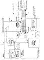
この点について、図1は、キャッシュメモリ12において提供される例示的なキャッシュメモリエラー検出回路10の概略図である。キャッシュメモリ12は、タグアレイ14およびデータアレイ16を備える。キャッシュメモリ12は、タグアレイ14およびデータアレイ16においてキャッシュエントリ18(0)〜18(N)を確立することができ、「N+1」は、キャッシュメモリ12内のキャッシュエントリ18の数である。キャッシュエントリ18(0)〜18(N)は、関連するタグ20(0)〜20(N)をタグアレイ14に記憶することによって確立される。キャッシュエントリ18(0)〜18(N)の確立はまた、対応するデータエントリ22(0)〜22(N)をデータアレイ16に記憶することを含む。データエントリ22(0)〜22(N)は、上位レベルキャッシュメモリまたはメインメモリなどの、上位レベルメモリに記憶されたデータに対応し得る。キャッシュエントリ18(0)〜18(N)を確立すると、各キャッシュエントリ18(0)〜18(N)に関連付けられた有効インジケータ24(0)〜24(N)は、キャッシュエントリ18(0)〜18(N)の有効性を示す有効状態(たとえば、論理高「1」を記憶する)に設定される。キャッシュエントリ18(0)〜18(N)がもはや有効ではない場合、もはや有効ではないキャッシュエントリ18(0)〜18(N)のための対応する有効インジケータ24(0)〜24(N)は、キャッシュエントリ18(0)〜18(N)を無効化するために無効状態(たとえば、論理低「0」を記憶する)に変更され得る。有効インジケータ24(0)〜24(N)は、それぞれのキャッシュエントリ18(0)〜18(N)についてキャッシュミスまたは他のエラーが生成されるべきかどうかを判断するために使用され得る。
In this regard, FIG. 1 is a schematic diagram of an exemplary cache memory
引き続き図1を参照すると、キャッシュエントリ18(0)〜18(N)内のキャッシュエントリ18を無効化することが望まれるとき、無効化動作が、無効化されるべきキャッシュエントリ18に対して実行され得る。無効化動作において1つのキャッシュエントリ18が無効化され得るか、またはキャッシュメモリ12に対して実行されるフラッシュ無効化動作の一部としてキャッシュメモリ12全体もしくはその複数のキャッシュエントリ18(0)〜18(N)が無効化され得る。図1のキャッシュメモリ12内のキャッシュエントリ18(0)〜18(N)のうちの1つまたは複数に対して実行される無効化動作は、無効化イネーブル入力28上で受信される無効化イネーブル信号26の受信時に開始される。それに応じて、キャッシュメモリ12は、無効化されたキャッシュエントリ18(0)〜18(N)に関連付けられた有効インジケータ24(0)〜24(N)を無効状態に設定する。フラッシュ無効化動作が、すべてのキャッシュエントリ18(0)〜18(N)を無効化するためにキャッシュメモリ12に対して実行された場合、キャッシュメモリ12は、すべてのキャッシュエントリ18(0)〜18(N)に対応するすべての有効インジケータ24(0)〜24(N)の状態を無効状態に設定する。
Still referring to FIG. 1, when it is desired to invalidate a
引き続き図1を参照すると、無効化動作後に、ただしキャッシュエントリ18(0)〜18(N)の再確立の前に、キャッシュエントリ18(0)〜18(N)のための有効インジケータ24(0)〜24(N)が有効状態を示す場合、キャッシュエントリ18(0)〜18(N)に関連付けられた有効インジケータ24(0)〜24(N)においてビットフリップが発生したことがわかる。これは、キャッシュエントリ18(0)〜18(N)の再確立の前の無効化動作後は、有効インジケータ24(0)〜24(N)が、(キャッシュヒットに関する)有効状態ではなく、(キャッシュミスに関する)無効状態を示すはずであるからである。したがって、以下でより詳細に説明するように、有効インジケータ24(0)〜24(N)がキャッシュメモリ12内のアクセスされたキャッシュエントリ18(0)〜18(N)の有効状態を示すとき、キャッシュメモリエラー検出回路10において提供される冗長情報インジケータ検証回路30は、キャッシュエントリ18(0)〜18(N)の再確立の前に無効化動作がキャッシュエントリ18(0)〜18(N)に対して実行されたかどうかを判断することができる。キャッシュエントリ18(0)〜18(N)の再確立の前に無効化動作がキャッシュエントリ18(0)〜18(N)に対して実行された場合、図1のキャッシュメモリエラー検出回路10は、キャッシュエントリ18(0)〜18(N)のための有効インジケータ24(0)〜24(N)が有効インジケータ24(0)〜24(N)におけるビットフリップのせいで有効状態を示していても、アクセスされたキャッシュエントリ18(0)〜18(N)に対するキャッシュミスを生成させるかまたはエラーを生成することができる。
Still referring to FIG. 1, after the invalidation operation, but before the re-establishment of cache entries 18 (0) -18 (N), valid indicators 24 (0) for cache entries 18 (0) -18 (N) ) -24 (N) indicates a valid state, it can be seen that a bit flip has occurred in the valid indicators 24 (0) -24 (N) associated with the cache entries 18 (0) -18 (N). This means that after the invalidation operation prior to the re-establishment of cache entries 18 (0) -18 (N), valid indicators 24 (0) -24 (N) are not in a valid state (with respect to cache hits) This is because it should indicate an invalid state (for a cache miss). Thus, as described in more detail below, when valid indicators 24 (0) -24 (N) indicate the valid state of accessed cache entries 18 (0) -18 (N) in cache memory 12, The redundancy information
引き続き図1を参照すると、アクセスされたキャッシュエントリ18(0)〜18(N)が、ビットフリップが発生するなどのエラーを生じたかどうかを示すために、キャッシュエントリエラーインジケータ34がキャッシュエントリエラーインジケータライン32上で提供される。図1に示す一例として、キャッシュエントリエラーインジケータ34は、非限定的な例としてキャッシュヒット/ミスインジケータライン42上でキャッシュヒット/ミスインジケータ40を生成するキャッシュヒット/ミスインジケータ回路38への入力として、キャッシュメモリエラー(たとえば、パリティエラー)を示す他の任意選択の入力36と組み合わせられ得る。別の例として、キャッシュエントリエラーインジケータ34は、キャッシュエラー生成および/または報告とは別に、アクセスされたキャッシュエントリ18(0)〜18(N)のための有効インジケータ24(0)〜24(N)におけるエラーを示すために提供される場合がある。また別の例として、キャッシュエントリエラーインジケータ34は、エラー訂正コード(ECC)を使用して前方誤り復元を生成するか、または所望のチェックポイントにリセットすることによって後方誤り復元を生成するために使用され得る。
Still referring to FIG. 1, a cache entry error indicator 34 is used to indicate whether the accessed cache entry 18 (0) -18 (N) has caused an error, such as a bit flip. Offered on
図1のキャッシュメモリエラー検出回路10のさらなる例示的な詳細について説明する前に、図1のキャッシュメモリエラー検出回路10がどのようにして無効化動作後の有効インジケータ24(0)〜24(N)におけるビットフリップを検出し得るかを説明するために、本明細書では最初に図2について説明する。この点について、図2は、図1のキャッシュメモリ12内のキャッシュエントリ18(0)について実行される一連の例示的なイベントを示す表44を示している。しかしながら、この例はキャッシュエントリ18(1)〜18(N)にアクセスすることにも適用されることに留意されたい。表44は、無効化動作後のキャッシュエントリ18(0)のための有効インジケータ24(0)におけるビットフリップの発生と、ビットフリップを検出する図1のキャッシュメモリエラー検出回路10の能力とを例示するものである。
Before describing further exemplary details of the cache memory
この点について、図1のキャッシュメモリ12内のキャッシュエントリ18(0)を例に取ると、キャッシュエントリ18(0)は、図2の確立イベント52によってキャッシュメモリ12において確立されるものとして示されている。有効インジケータ24(0)は、キャッシュエントリ18(0)の確立の間、有効状態(たとえば、「1」)に設定される。この例では無効化インターバルカウント48(たとえば、「10」)の形の現在の無効化インターバルステートは、確立時にキャッシュエントリ18(0)に記憶される冗長情報インジケータ46(0)として使用される。したがって、この実施形態では、冗長情報インジケータ46(0)は、実際の、符号化されていない形式の無効化インターバルカウント48を含む。キャッシュメモリエラー検出回路10は、各キャッシュエントリ18(0)〜18(N)に対応する冗長情報インジケータ46(0)〜46(N)と、図1のキャッシュメモリエラー検出回路10内の、この例では無効化インターバルカウンタ50の形の無効化インターバルインジケータによって提供される現在の無効化インターバルカウント48とを使用して、ビットフリップを検出する。キャッシュエントリ18(0)に対するタグ20(0)も確立される。無効化インターバルインジケータは、限定はしないが、無効化インターバルステートとは異なる状態または他のステータスなどの任意のタイプの所望のインジケータを記憶するために、カウンタ以外の他の形で提供される場合があることに留意されたい。
In this regard, taking the cache entry 18 (0) in the cache memory 12 of FIG. 1 as an example, the cache entry 18 (0) is shown as being established in the cache memory 12 by the
次に、引き続き図2を参照すると、無効化動作54がキャッシュエントリ18(0)に対して実行される。無効化動作54は、上記で説明したように、キャッシュエントリ18(0)を無効化するために、キャッシュエントリ18(0)のための有効インジケータ24(0)の有効性状態を無効状態(たとえば、「0」)に設定する。現在の無効化インターバルカウント48はまた、無効化動作54を記録するために、この例では増分されることによって進められる。現在の無効化インターバルカウント48は増分されているが、キャッシュエントリ18(0)内の冗長情報インジケータ46(0)は同じままであることに留意されたい。以下で説明するように、この情報は、キャッシュエントリ18(0)に対する前の確立イベント52の後に無効化動作54が発生したと判断するために、後で使用される。
Next, with continued reference to FIG. 2, an
引き続き図2を参照すると、例示のために、この例では有効インジケータ24(0)においてビットフリップ(たとえば、「0」から「1」へのビットフリップ)を発生させる放射線イベント56が発生すると次に仮定する。しかしながら、上記で説明したように、キャッシュエントリ18(0)内の冗長情報インジケータ46(0)は、現在の無効化インターバルカウント48に等しくない、すなわち、無効化動作54が発生しており、この場合、有効インジケータ24(0)が無効状態(たとえば、「0」)を含むと予想される。したがって、キャッシュエントリ18(0)が再確立される前にアクセスイベント58において後でアクセスされたとき、キャッシュエントリ18(0)のための有効インジケータ24(0)は有効状態を示す。しかしながら、上記で述べたように、キャッシュエントリ18(0)は、前の無効化動作54のせいで実際には有効ではない。現在の無効化インターバルカウント48が無効化動作54の結果として増分されたので、現在の無効化インターバルカウント48は、キャッシュエントリ18(0)が確立されたときにキャッシュエントリ18(0)に記憶された冗長情報インジケータ46(0)と一致しない。したがって、キャッシュメモリエラー検出回路10は、この不一致を、無効化動作54に続く有効インジケータ24(0)において発生したビットフリップを検出する方法として判断するように構成される場合がある。以下でより詳細に説明するように、キャッシュメモリエラー検出回路10は、有効インジケータ24(0)がビットフリップのせいで有効状態を示していても、誤ったキャッシュヒットが生成されないように、キャッシュエントリ18(0)に対するアクセスイベント58にキャッシュミスを生成させるかまたはエラーを生成することができる。
Still referring to FIG. 2, for illustrative purposes, in this example, when a
この点について、次に図1のキャッシュメモリエラー検出回路10の例示的なさらなる詳細について説明する。この点について、図1のキャッシュメモリエラー検出回路10内の冗長情報インジケータ検証回路30は、無効化インターバルカウンタ50に基づいて、キャッシュエントリ18(0)〜18(N)の再確立の前に無効化動作(図示せず)がいつ発生したかを判断する。無効化インターバルカウンタ50は、この例ではキャッシュメモリ12内のキャッシュエントリ18(0)〜18(N)に対して実行された無効化動作ごとに無効化インターバルカウント48を増分する。無効化インターバルカウント48は、キャッシュメモリ12においてキャッシュエントリ18(0)〜18(N)が確立されたときに、冗長情報インジケータ生成回路60によってキャッシュエントリ18(0)〜18(N)に冗長情報インジケータ46(0)〜46(N)として記憶される。
In this regard, exemplary further details of the cache memory
無効化インターバルカウンタ50は、1(1)だけ無効化インターバルカウント48を増分するように構成され得るか、または1(1)以外の値だけ無効化インターバルカウント48を増分することが望まれ得る。無効化インターバルカウンタ50は、無効化インターバルカウンタ50によって使用されるビット数に基づいて、様々な無効化インターバルカウント値にわたって無効化インターバルカウント48を増分するように構成され得る。たとえば、無効化インターバルカウンタ50によって2(2)ビットが使用される場合、図2で説明するように無効化インターバルカウント48について4つ(4)の考えられる値(たとえば、「00」、「01」、「10」、および「11」)があり、様々な8つ(8)の値に3(3)ビットが与えられる。無効化インターバル構成設定62に基づいて、無効化インターバルカウント48に対する無効化インターバルカウント値の範囲を構成するかまたは無効化インターバルカウンタ50を使用不可にすることさえも可能であり得る。無効化インターバルカウント48は、無効化インターバルカウンタ50によって冗長情報インジケータ生成回路60に提供され、冗長情報インジケータ検証回路30にも提供される。
Invalidation interval counter 50 may be configured to increment
引き続き図1を参照すると、後でアクセスされたキャッシュエントリ18(0)〜18(N)のための有効インジケータ24(0)〜24(N)が有効状態を示す場合、キャッシュメモリエラー検出回路10内の冗長情報インジケータ検証回路30は、アクセスされたキャッシュエントリ18(0)〜18(N)の最後の確立以降に無効化動作が発生したかどうかを確認する。冗長情報インジケータ検証回路30は、現在の無効化インターバルカウント48と、キャッシュエントリ18(0)〜18(N)が確立されたときに冗長情報インジケータ46(0)〜46(N)としてキャッシュエントリ18(0)〜18(N)に記憶された無効化インターバルカウントとに基づいて、無効化動作が発生したかどうかを確認する。キャッシュエントリ18(0)〜18(N)が確立されたときにキャッシュエントリ18(0)〜18(N)に記憶された無効化インターバルカウントが、アクセスされたキャッシュエントリ18(0)〜18(N)のための有効インジケータ24(0)〜24(N)に関連付けられた現在の無効化インターバルカウント48と一致しない場合、これは不一致をもたらす。この不一致は、無効化動作後にキャッシュエントリ18(0)〜18(N)に関連付けられた有効インジケータ24(0)〜24(N)においてビットフリップが発生したという指標である。これは、無効化動作が有効インジケータ24(0)〜24(N)を強制的に無効状態にしたので、無効化動作後は、アクセスされたキャッシュエントリ18(0)〜18(N)のための有効インジケータ24(0)〜24(N)が、有効状態ではなく、無効状態を示すはずであるからである。
Still referring to FIG. 1, if the valid indicators 24 (0) -24 (N) for cache entries 18 (0) -18 (N) accessed later indicate a valid state, the cache memory
したがって、図1のこの例では、キャッシュメモリエラー検出回路10内の冗長情報インジケータ検証回路30は、アクセスされたキャッシュエントリ18(0)〜18(N)に関連付けられた有効インジケータ24(0)〜24(N)においてビットフリップが検出されるときに(キャッシュヒットではなく)キャッシュミスを生成させるかまたはエラーを生成するように構成される。キャッシュエントリ18(0)〜18(N)に関連付けられた冗長情報インジケータ46(0)〜46(N)と一致しない、無効化インターバルカウンタ50によって提供された現在の無効化インターバルカウント48は、無効化動作後に有効インジケータ24(0)〜24(N)においてビットフリップが発生したという指標である。検出された無効化動作後にビットフリップが検出されたとき、キャッシュエントリ18(0)〜18(N)に対応するデータアレイ16に記憶されたデータエントリ22(0)〜22(N)を使用することを回避するために、キャッシュミスまたは他のエラーが生成される。アクセスされたキャッシュエントリ18(0)〜18(N)についての誤った有効インジケータ24(0)〜24(N)状態が検出されなかった場合、キャッシュメモリ12は、本当はキャッシュミスとすべきところを、誤ったキャッシュヒットを生成したであろう。
Thus, in this example of FIG. 1, the redundant information
この点について、図3は、キャッシュメモリ12内のキャッシュエントリ18(0)〜18(N)に対して実行された無効化動作(図示せず)ごとに、図1のキャッシュメモリエラー検出回路10の無効化インターバルカウンタ50における無効化インターバルカウント48を増分するための例示的なプロセスを示すフローチャートである。図1および図3を参照すると、無効化インターバルカウンタ50は、無効化イネーブル信号26を受信する(ブロック64)。次いで、無効化インターバルカウンタ50は、無効化イネーブル信号26を受信したことに基づいて、無効化インターバルカウント48を増分する(ブロック66)。無効化インターバルカウンタ50は、無効化インターバル構成設定62によって設定された構成可能な増分量だけ無効化インターバルカウント48を増分し得る。無効化インターバルカウンタ50はまた、無効化インターバル構成設定62に基づいて、使用不可にされるかまたは固定の無効化インターバルカウント48値に設定され得る。
In this regard, FIG. 3 illustrates the cache memory
この点について、図4は、確立時にキャッシュエントリ18(0)〜18(N)に冗長情報インジケータ46(0)〜46(N)を記憶するために無効化インターバルカウンタ50から現在の無効化インターバルカウント48を受信する、図1のキャッシュメモリエラー検出回路10内の冗長情報インジケータ生成回路60の例示的なプロセスを示すフローチャートである。図1および図4を参照すると、冗長情報インジケータ生成回路60は、確立されるべきキャッシュエントリ18(0)〜18(N)において提供されたタグ20(0)〜20(N)を受信するように構成される(ブロック68)。冗長情報インジケータ生成回路60はまた、無効化インターバルカウンタ50によって提供された現在の無効化インターバルカウント48を受信するように構成される(ブロック70)。冗長情報インジケータ生成回路60は、無効化インターバルカウンタ50から受信された現在の無効化インターバルカウント48を確立されているキャッシュエントリ18(0)〜18(N)に記憶する(ブロック72)。この例では、冗長情報インジケータ46(0)〜46(N)は現在の無効化インターバルカウント48であり、冗長情報インジケータ46(0)〜46(N)としてキャッシュエントリ18(0)〜18(N)に記憶される。冗長情報インジケータ46(0)〜46(N)は、キャッシュエントリ18(0)〜18(N)に関連付けられた有効インジケータ24(0)〜24(N)を検証するために、キャッシュメモリエラー検出回路10の冗長情報インジケータ検証回路30によって使用される。
In this regard, FIG. 4 shows the current invalidation interval from invalidation interval counter 50 to store redundancy information indicators 46 (0) -46 (N) in cache entries 18 (0) -18 (N) when established. 2 is a flowchart illustrating an exemplary process of redundant information
この点について、図5は、キャッシュメモリ12内のアクセスされたキャッシュエントリ18(0)〜18(N)の有効インジケータ24(0)〜24(N)においてビットフリップが発生したかどうかを検出する、図1のキャッシュメモリエラー検出回路10内の冗長情報インジケータ検証回路30の例示的なプロセスを示すフローチャートである。ビットフリップが発生したかどうかを検出することは、キャッシュエントリ18(0)〜18(N)の確立の間のキャッシュエントリ18(0)〜18(N)に関連付けられた冗長情報インジケータ46(0)〜46(N)と、無効化インターバルカウンタ50における現在の無効化インターバルカウント48を比較することに基づく。図1および図5を参照すると、冗長情報インジケータ検証回路30は、キャッシュエントリ18(0)〜18(N)に記憶された冗長情報インジケータ46(0)〜46(N)に基づいて、アクセスされているキャッシュエントリ18(0)〜18(N)に対応する有効インジケータ24(0)〜24(N)を検証する。冗長情報インジケータ検証回路30は、アクセスされたキャッシュエントリ18(0)〜18(N)のための有効インジケータ24(0)〜24(N)が有効状態を示すことに応じて、アクセスされたキャッシュエントリ18(0)〜18(N)のための冗長情報インジケータ46(0)〜46(N)を受信する(ブロック74)。冗長情報インジケータ検証回路30はまた、無効化インターバルカウンタ50から現在の無効化インターバルカウント48を受信する(ブロック76)。冗長情報インジケータ検証回路30は、アクセスされたキャッシュエントリ18(0)〜18(N)に関連付けられた冗長情報インジケータ46(0)〜46(N)を現在の無効化インターバルカウント48と比較する(ブロック78)。現在の無効化インターバルカウント48が、アクセスされたキャッシュエントリ18(0)〜18(N)のための有効インジケータ24(0)〜24(N)が有効状態を示したときに冗長情報インジケータ46(0)〜46(N)に記憶された無効化インターバルカウントと一致しない場合、これは、無効化動作後にキャッシュエントリ18(0)〜18(N)に関連付けられた有効インジケータ24(0)〜24(N)においてビットフリップが発生したという指標である。これは、無効化動作が有効インジケータ24(0)〜24(N)を強制的に無効状態にするので、無効化動作後は、アクセスされたキャッシュエントリ18(0)〜18(N)のための有効インジケータ24(0)〜24(N)が、有効状態ではなく、無効状態を示すはずであるからである。一致は、キャッシュエントリ18(0)〜18(N)の確立と確立されたキャッシュエントリ18(0)〜18(N)のアクセスの両方が同じ無効化インターバルにおいて発生したことを示す。キャッシュエントリエラーインジケータ34は、冗長情報インジケータ46(0)〜46(N)と現在の無効化インターバルカウント48を比較することに基づいて、この態様ではアクセスされたキャッシュエントリ18(0)〜18(N)のための有効インジケータ24(0)〜24(N)においてビットフリップが発生したかどうかを示す(ブロック80)。
In this regard, FIG. 5 detects whether a bit flip has occurred in valid indicators 24 (0) -24 (N) of accessed cache entries 18 (0) -18 (N) in cache memory 12. 2 is a flowchart illustrating an exemplary process of a redundant information
図1のキャッシュメモリエラー検出回路10は、耐放射性化を用いて有効インジケータ24(0)〜24(N)を保護することなく、または有効インジケータ24(0)〜24(N)をキャッシュエントリ18(0)〜18(N)のためのパリティなどのエラー検出コードに含めることなしに、キャッシュメモリ12内の有効インジケータ24(0)〜24(N)におけるビットフリップを検出することができる。キャッシュメモリエラー検出回路10は、キャッシュエントリ18(0)〜18(N)が確立されたときにキャッシュメモリ12内のキャッシュエントリ18(0)〜18(N)に記憶される無効化インターバルカウント48によって、ビットフリップを検出することができる。有効インジケータ24(0)〜24(N)がキャッシュエントリ18(0)〜18(N)のためのエラー検出コードに含まれていた場合、有効インジケータ24(0)〜24(N)を強制的に無効状態にすることに加えて、各無効化されたキャッシュエントリ18(0)〜18(N)のエラー検出コードがキャッシュメモリフラッシュ無効化動作において再計算されなければならず、したがって、フラッシュ無効化動作のレイテンシを増加させる。しかしながら、無効化インターバルカウント48が確立時に各キャッシュエントリ18(0)〜18(N)に記憶される場合、キャッシュメモリ12内のキャッシュエントリ18(0)〜18(N)ごとに追加のビットが含まれなければならない。キャッシュエントリ18(0)〜18(N)が確立されたときに無効化インターバルカウント48を記憶するためにキャッシュメモリ12内の各キャッシュエントリ18(0)〜18(N)において追加のビットを提供する必要性を回避するために、無効化インターバルカウント48は代替的に、キャッシュエントリ18(0)〜18(N)に記憶された既存のキャッシュエントリエラー検出コード(たとえば、パリティ)とともに符号化され得る。
The cache memory
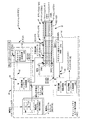
図6に関して、図1と同様のキャッシュエントリエラー検出を提供する例示的なキャッシュメモリエラー検出回路10(1)の概略図が提供される。図6のキャッシュメモリエラー検出回路10(1)は、共通の要素番号を共有する、図1のキャッシュメモリエラー検出回路10と共通のいくつかの要素を含む。したがって、ここでは、これらの共通の要素について改めて説明しない。図6のキャッシュメモリエラー検出回路10(1)はまた、キャッシュエントリ18(0)〜18(N)におけるビットフリップを検出する機能を提供する。キャッシュメモリエラー検出回路10(1)は、図1で前に説明した、少なくとも1つの無効化インターバルカウンタ50(0)〜50(M)から成る。キャッシュメモリエラー検出回路10(1)は、無効化インターバルカウント48(0)〜48(M)を冗長情報インジケータ生成回路60(1)と冗長情報インジケータ検証回路30(1)の両方に提供する。
With reference to FIG. 6, a schematic diagram of an exemplary cache memory error detection circuit 10 (1) that provides cache entry error detection similar to FIG. 1 is provided. The cache memory error detection circuit 10 (1) of FIG. 6 includes several elements in common with the cache memory
引き続き図6を参照すると、選択的な無効化動作の追跡を容易にするための関連する無効化インターバルカウント48(0)〜48(M)を含む、複数の無効化インターバルカウンタ50(0)〜50(M)が提供され得る。選択的な無効化動作は、キャッシュメモリ12(1)内のキャッシュエントリ18(0)〜18(N)のすべてまたはサブセットに対して実行されるフラッシュ無効化動作ではなく、キャッシュメモリ12(1)内の連続していてもよく連続していなくてもよいキャッシュエントリ18(0)〜18(N)の一部分のみに対して実行される無効化動作である。選択的な無効化動作は、特定の無効化インターバルカウンタ50(0)〜50(M)および対応する無効化インターバルカウント48(0)〜48(M)に関連付けられるべき、連続していてもよく連続していなくてもよいキャッシュエントリ18(0)〜18(N)のサブセットを考慮する。選択的な無効化動作は、限定はしないが、権限、セキュリティ、例外レベル、異なる動作モード、エントリのタイプなどに基づいて決定され得る。このようにして、図6のキャッシュメモリエラー検出回路10(1)は、無効化イネーブル信号26に応答して、キャッシュエントリ18(0)〜18(N)の一部分のみに関連付けられた無効化インターバルカウント48(0)〜48(M)を増分するように構成され得る。
Still referring to FIG. 6, a plurality of invalidation interval counters 50 (0)-including associated invalidation interval counts 48 (0) -48 (M) to facilitate tracking selective invalidation operations. 50 (M) may be provided. The selective invalidation operation is not a flush invalidation operation performed on all or a subset of cache entries 18 (0) -18 (N) in cache memory 12 (1), but cache memory 12 (1) The invalidation operation is executed only for a part of the cache entries 18 (0) to 18 (N) which may or may not be continuous. Selective invalidation actions may be sequential, which should be associated with a specific invalidation interval counter 50 (0) -50 (M) and corresponding invalidation interval count 48 (0) -48 (M). Consider a subset of cache entries 18 (0) -18 (N) that may not be contiguous. The selective invalidation action may be determined based on, but not limited to, authority, security, exception level, different operating modes, entry type, and the like. In this manner, the cache memory error detection circuit 10 (1) of FIG. 6 is responsive to the invalidation enable
引き続き図6を参照すると、キャッシュメモリ12(1)は、この例では複数のデータアレイ16(0)〜16(X)を含み、データアレイ16の数は「X+1」に等しい。複数のデータアレイ16(0)〜16(X)の各々は、無効化インターバルカウンタ50(0)〜50(M)に関連付けられる。データアレイ16(0)〜16(X)はまた、権限、セキュリティ、例外レベル、異なる動作モード、エントリのタイプなどの、無効化動作が基づき得る共通のイベントリストを複数のデータアレイ16(0)〜16(X)が使用している場合、共通の無効化インターバルカウンタ50(0)〜50(M)を共有する。複数のキャッシュメモリ(図示せず)はそれぞれ、冗長情報インジケータ生成回路60(1)および冗長情報インジケータ検証回路30(1)を提供し得る。たとえば、複数のキャッシュメモリ(図示せず)によって提供された複数のキャッシュレベルは一緒に無効化する場合があり、したがって、キャッシュメモリ12(1)ごとまたはキャッシュメモリ12(1)のレベルごとの無効化インターバルカウンタ50(0)〜50(M)を不要にする。 Still referring to FIG. 6, the cache memory 12 (1) includes a plurality of data arrays 16 (0) to 16 (X) in this example, and the number of data arrays 16 is equal to “X + 1”. Each of the plurality of data arrays 16 (0) -16 (X) is associated with an invalidation interval counter 50 (0) -50 (M). Data arrays 16 (0) -16 (X) also have multiple data arrays 16 (0) with a common event list on which invalidation actions can be based, such as permissions, security, exception levels, different operating modes, entry types, etc. When ~ 16 (X) is used, the common invalidation interval counter 50 (0) ~ 50 (M) is shared. Each of the plurality of cache memories (not shown) may provide a redundant information indicator generation circuit 60 (1) and a redundant information indicator verification circuit 30 (1). For example, multiple cache levels provided by multiple cache memories (not shown) may invalidate together, and thus invalidate per cache memory 12 (1) or per level of cache memory 12 (1) Interval counters 50 (0) to 50 (M) are unnecessary.
引き続き図6を参照すると、冗長情報インジケータ生成回路60(1)は、アクセスされているキャッシュエントリ18(0)〜18(N)に関連付けられた無効化インターバルカウンタ50(0)〜50(M)によって提供された現在の無効化インターバルカウント48(0)〜48(M)を受信する。加えて、冗長情報インジケータ生成回路60(1)は、非限定的な例として、タグエラー検出コード生成回路84によって提供された第2の入力として、タグパリティ82の形でエラー検出コード81を受信する。タグエラー検出コード生成回路84は、キャッシュエントリ18(0)〜18(N)において受信されたタグ20(0)〜20(N)に基づいて、タグパリティ82を生成する。タグパリティ82は、タグ20(0)〜20(N)が破損したかどうかまたは他の点で予期せずに変化したかどうかをキャッシュメモリ12(1)が検出するのを可能にする、エラー検査の目的で使用される。この例では、冗長情報インジケータ生成回路60(1)は、タグパリティ82を受信し、受信された無効化インターバルカウント48(0)〜48(M)を符号化して、受信された無効化インターバルカウント48(0)〜48(M)の符号化されたバージョンをタグパリティ82の一部として提供する。この符号化の結果として、冗長情報インジケータ生成回路60(1)は、確立されるべきキャッシュエントリ18(0)〜18(N)に対応する、記憶されるべき冗長情報インジケータの符号化されたバージョン46'(1)(0)〜46'(1)(N)を出力する。
Still referring to FIG. 6, the redundancy information indicator generation circuit 60 (1) is responsible for the invalidation interval counter 50 (0) -50 (M) associated with the cache entry 18 (0) -18 (N) being accessed. The current invalidation interval count 48 (0) -48 (M) provided by is received. In addition, the redundant information indicator generation circuit 60 (1) receives the
タグパリティ82において無効化インターバルカウント48(0)〜48(M)を符号化することは、パリティ記憶のための追加のビットを必要とせずに無効化インターバルカウント48(0)〜48(M)を符号化する利益を可能にする。この形の符号化はまた、有効インジケータ24(0)〜24(N)およびタグ20(0)〜20(N)のエラー検出コード(たとえば、パリティ)検査を冗長情報インジケータ検証回路30(1)における単一の動作に組み合わせる利益をもたらす。次いで、記憶された符号化冗長情報インジケータ46'(1)(0)〜46'(1)(N)は、後でアクセスされたキャッシュエントリ18(0)〜18(N)に対応する有効インジケータ24(0)〜24(N)を検証するために使用される。しかしながら、以下でより詳細に説明するように、図6のキャッシュメモリ12(1)内のキャッシュエントリ18(0)〜18(N)においてビットフリップが検出された場合、有効インジケータ24(0)〜24(N)のみにおける場合に対立するものとして、キャッシュエントリ18(0)〜18(N)のどこかでビットフリップが発生した可能性がある。図6のキャッシュメモリ12(1)についてさらに説明するために、図7は、図6のキャッシュメモリ12(1)における一連の例示的なキャッシュエントリ18(0)イベントを示す表86を提供する。一例として、表86は、無効化動作の後の有効インジケータ24(0)におけるビットフリップの発生と、符号化冗長情報インジケータ46'(1)(0)および現在の無効化インターバルカウント48(0)を使用してキャッシュエントリ18(0)〜18(N)におけるビットフリップを検出する能力とを例示している。図7を参照すると、図示した例示的なイベントは、一連のキャッシュエントリ18(0)イベントから成る。キャッシュエントリ18(0)は最初に、確立イベント90において確立される。キャッシュエントリ18(0)の確立イベント90の際に、タグ20(0)がタグアレイ14に記憶される。加えて、有効インジケータ24(0)がキャッシュメモリ12(1)によって有効状態(たとえば、論理高または「1」)に設定される。この例での冗長情報インジケータ46(1)(0)は、冗長情報インジケータ生成回路60(1)によって現在の無効化インターバルカウント48(0)(たとえば、「10」)とともに符号化されて、タグアレイ14内のキャッシュエントリ18(0)に記憶される符号化冗長情報インジケータ46'(1)(0)を提供する。この例では、冗長情報インジケータ生成回路60(1)は、「排他的論理和」関数を使用して、タグ20(0)(たとえば、「0111」)とともに現在の無効化インターバルカウント48(0)(たとえば、「10」)を符号化し、結果としてキャッシュエントリ18(0)に対応する「00」の値が記憶される。何らかの時点で、受信された無効化イネーブル信号26(図示せず)によって示される無効化動作92が、少なくとも1つのキャッシュエントリ18(0)を無効化する。無効化動作92が発生すると、キャッシュメモリ12(1)は有効インジケータ24(0)を無効状態(たとえば、論理低または「0」)に設定する。加えて、無効化動作92を示す無効化イネーブル信号26を受信したことに応じて、現在の無効化インターバルカウント48(0)が構成された間隔ごとに無効化インターバルカウンタ50(0)によって増分される(たとえば、「11」)。しかしながら、現在の無効化インターバルカウント48(0)は増分されるが、符号化された無効化インターバルカウント48(0)を有する記憶された符号化冗長情報インジケータ46'(1)(0)は変わらないままである。
Encoding the invalidation interval counts 48 (0) -48 (M) in the
引き続き図7を参照すると、キャッシュメモリエラー検出回路10(1)は、無効化動作92に続くキャッシュエントリ18(0)〜18(N)におけるビットフリップを検出するように構成される。後でアクセスされたキャッシュエントリ18(0)のための有効インジケータ24(0)が有効状態を示す場合、キャッシュメモリエラー検出回路10(1)は、無効化インターバルカウンタ50(0)によって提供された現在の無効化インターバルカウント48(0)の符号化されたバージョンが、キャッシュエントリ18(0)が確立されたときの冗長情報インジケータ46(1)(0)と一致することを確認する。現在の無効化インターバルカウント48(0)は、冗長情報インジケータ46(1)(0)の場合と同様の方法で符号化される。したがって、記憶された冗長情報インジケータ46(1)(0)と一致する現在の無効化インターバルカウント48(0)は、キャッシュエントリ18(0)を確立し、それにアクセスするために同じ無効化インターバルカウント48(0)が使用されたことを意味する。したがって、無効化動作92は、キャッシュエントリ18(0)へのアクセスの前に実行されなかった。しかしながら、キャッシュエントリ18(0)に対するアクセスイベント96の際に、現在の無効化インターバルカウント48(0)の符号化されたバージョンがキャッシュエントリ18(0)に関連付けられた無効化インターバルカウント48(0)と一致しない場合、これは、アクセスされたキャッシュエントリ18(0)のための有効インジケータ24(0)が有効状態を示していても、無効化動作92に続いてアクセスされたキャッシュエントリ18(0)においてビットフリップが発生したという指標である。このようにして、キャッシュメモリ12(1)は、本当はキャッシュミスとすべきところを、誤ったキャッシュヒットを生成する場合がある。
With continued reference to FIG. 7, cache memory error detection circuit 10 (1) is configured to detect bit flips in cache entries 18 (0) -18 (N) following
図8は、キャッシュエントリ18(0)〜18(N)におけるビットフリップを検出するために図6のキャッシュメモリ12(1)内のキャッシュメモリエラー検出回路10(1)において提供され得る例示的な冗長情報インジケータ検証回路30(1)の概略図のさらなる詳細を提供する。冗長情報インジケータ検証回路30(1)は、キャッシュエントリ18(0)〜18(N)の確立時に無効化インターバルカウンタ50(0)〜50(M)からの無効化インターバルカウント48(0)〜48(M)とともに符号化された、記憶された符号化冗長情報インジケータ46'(1)(0)〜46'(1)(N)に基づいて、キャッシュエントリ18(0)〜18(N)におけるビットフリップを検出するように構成される。図8を参照すると、冗長情報インジケータ検証回路30(1)は、有効インジケータ24(0)〜24(N)を適切に有効であると判断するために、記憶された符号化冗長情報インジケータ46'(1)(0)〜46'(1)(N)を現在の冗長情報インジケータ98と比較するように構成される。現在の冗長情報インジケータ98の生成について、以下で説明する。冗長情報インジケータ比較回路100は、キャッシュエントリ18(0)〜18(N)の確立時に符号化された符号化冗長情報インジケータ46'(1)(0)〜46'(1)(N)をキャッシュエントリ18(0)〜18(N)へのアクセス時に生成された現在の冗長情報インジケータ98と比較するために提供される。符号化冗長情報インジケータ46'(1)(0)〜46'(1)(N)と現在の冗長情報インジケータ98を比較することによって、冗長情報インジケータ検証回路30(1)は、キャッシュエントリ18(0)〜18(N)の確立の後かつキャッシュエントリ18(0)〜18(N)へのアクセスの前に無効化動作が発生したかどうかを判断することが可能である。符号化冗長情報インジケータ46'(1)(0)〜46'(1)(N)と現在の冗長情報インジケータ98が等しくない場合、これは、キャッシュエントリ18(0)〜18(N)の確立に続いて無効化動作が発生しており、関連する有効インジケータ24(0)〜24(N)が無効状態に設定されるべきであるという指標である。
FIG. 8 illustrates an example that may be provided in the cache memory error detection circuit 10 (1) in the cache memory 12 (1) of FIG. 6 to detect bit flips in the cache entries 18 (0) -18 (N). Further details of a schematic diagram of the redundant information indicator verification circuit 30 (1) is provided. Redundant information indicator verification circuit 30 (1) is configured to invalidate interval counts 48 (0) -48 from invalidation interval counters 50 (0) -50 (M) when cache entries 18 (0) -18 (N) are established. In cache entries 18 (0) -18 (N), based on stored encoded redundancy information indicators 46 '(1) (0) -46' (1) (N), encoded with (M) Configured to detect bit flips. Referring to FIG. 8, the redundant information indicator verification circuit 30 (1) may store the stored coded
引き続き図8を参照すると、現在の冗長情報インジケータ98は、冗長情報インジケータ検証回路30(1)において提供される第2の冗長情報インジケータ生成回路102によって生成される。第2の冗長情報インジケータ生成回路102は、非限定的な例として、図6のタグエラー検出コード回路106によって提供されたタグパリティ104の形で、現在生成されたエラー検出コード103を受信する。第2の冗長情報インジケータ生成回路102はまた、無効化インターバルカウンタ50(0)〜50(M)によって提供された現在の無効化インターバルカウント48(0)〜48(M)を受信する。無効化インターバルカウント48(0)〜48(M)は、キャッシュエントリ18(0)〜18(N)へのアクセス時の現在の無効化インターバルカウント48(0)〜48(M)を表す。現在の冗長情報インジケータ98は、符号化冗長情報インジケータ46'(1)(0)〜46'(1)(N)と同様の方式で第2の冗長情報インジケータ生成回路102によって生成される。
With continued reference to FIG. 8, the current
引き続き図8を参照すると、第2の冗長情報インジケータ生成回路102は、現在の冗長情報インジケータ98を生成するためにORベースの関数を実施する複数の論理ゲート108を使用する。たとえば、論理ゲート108はこの例ではXORゲートであるが、例としてORゲートおよび/またはNORゲートなどのORベースのゲートを含む他のゲートも利用され得る。非限定的な例として、無効化インターバルカウント48(0)〜48(M)が「10」であり、タグ20(0)〜20(N)が「0111」である場合、第1のパリティ生成回路110は、「10」+「0111」すなわち「100111」の結合または連結された値の奇数ビットに対して「排他的論理和」関数を実行する。結合または連結された値「100111」の第1の2(2)ビットは無効化インターバルカウント48(0)〜48(M)であり、第2の4(4)ビットはキャッシュエントリ18(0)〜18(N)内のタグ20(0)〜20(N)である。結合または連結された値「100111」の奇数ビットに対する「排他的論理和」関数の結果は「0」であり、これは符号化冗長情報インジケータ46'(1)(0)〜46'(1)(N)の第1のビットになる。第2のパリティ生成回路112では、タグパリティ104の偶数ビットおよび無効化インターバルカウント48(0)〜48(M)の偶数ビットは、偶数ビットの各々に適用される同じ「排他的論理和」関数を使用して符号化される。その結果は、符号化冗長情報インジケータ46'(1)(0)〜46'(1)(N)の第2のビットを形成する。得られた符号化冗長情報インジケータ46'(1)(0)〜46'(1)(N)は、奇数ビットおよび偶数ビットの各々に適用される「排他的論理和」関数を介して無効化インターバルカウント48(0)〜48(M)とともに符号化されたタグパリティ104になる。「排他的論理和」関数に加えて他のデジタル論理関数が使用され得ることに留意されたい。
With continued reference to FIG. 8, the second redundant information
引き続き図6および図8を参照すると、冗長情報インジケータ検証回路30(1)は、タグパリティ104を表す複数のビットを受信するように構成され得、その結果、タグパリティ[0]114は最初のビットまたは最下位ビットを表し、タグパリティ[Y]116は最後のビットまたは最上位ビットを表し、ここで、タグパリティ104内にY個のビットがある。冗長情報インジケータ検証回路30(1)はまた、無効化インターバルカウント48(0)〜48(M)を表す複数のビットを受信するように構成され得、その結果、無効化インターバルカウント[0]118は最初のビットまたは最下位ビットを表し、無効化インターバルカウント[Z]120は最後のビットまたは最上位ビットを表し、ここで、無効化インターバルカウント48(0)〜48(M)内にZ個のビットがある。キャッシュエントリ18(0)〜18(N)に対応する、得られた符号化冗長情報インジケータ46'(1)(0)〜46'(1)(N)は、タグアレイ14に記憶される。
With continued reference to FIGS. 6 and 8, redundant information indicator verification circuit 30 (1) may be configured to receive a plurality of bits representing
生成されると、現在の冗長情報インジケータ98は、一致が存在するかどうかを判断するために、冗長情報インジケータ比較回路100によって、記憶された符号化冗長情報インジケータ46'(1)(0)〜46'(1)(N)と比較される。一致が存在する場合、これは、同じ無効化インターバルカウント48(0)〜48(M)によって表されるように、同じ無効化インターバルにおいてキャッシュエントリ18(0)〜18(N)の確立およびキャッシュエントリ18(0)〜18(N)へのアクセスが発生したので、有効インジケータ24(0)〜24(N)は有効であるはずであるという指標である。比較の結果として、冗長情報インジケータ比較回路100は、キャッシュエントリ18(0)〜18(N)においてビットフリップが発生したかどうかをシグナリングするキャッシュエントリエラーインジケータ122を生成する。
Once generated, the current
引き続き図6を参照すると、キャッシュメモリ12(1)内の例示的な冗長情報インジケータ生成回路60(1)の概略図のさらなる詳細が図9で提供される。冗長情報インジケータ生成回路60(1)は、確立されるべきキャッシュエントリ18(0)〜18(N)に対応する符号化エラー検出コード(たとえば、パリティ)およびキャッシュエントリ18(0)〜18(N)が確立されたときの無効化インターバルカウント48(0)〜48(M)に基づいて、符号化冗長情報インジケータ46'(1)(0)〜46'(1)(N)を生成するように構成される。図9の冗長情報インジケータ生成回路60(1)を参照すると、符号化冗長情報インジケータ46'(1)(0)〜46'(1)(N)を生成するためにタグパリティ82とともに無効化インターバルカウント48(0)〜48(M)を符号化する1つの方法が示されている。この例では、冗長情報インジケータ生成回路60(1)は、タグパリティ82において無効化インターバルカウント48(0)〜48(M)を符号化するために「排他的論理和」関数を実施する複数の論理ゲート108を使用する。冗長情報インジケータ生成回路60(1)は、冗長情報インジケータ検証回路30(1)と類似している。「排他的論理和」関数は、デジタル回路におけるエラー検出コードとしてのパリティ生成を実施するために使用され得る。この例では、冗長情報インジケータ生成回路60(1)は、「排他的論理和」を受信された入力の奇数ビットおよび偶数ビットの各々に適用することに基づいて、符号化冗長情報インジケータ46'(1)(0)〜46'(1)(N)を生成する。第1のパリティ生成回路110では、タグパリティ82の奇数ビットおよび無効化インターバルカウント48(0)〜48(M)の奇数ビットは、奇数ビットの各々に適用される「排他的論理和」関数を使用して符号化される。その結果は、符号化冗長情報インジケータ46'(1)(0)〜46'(1)(N)の第1のビットを形成する。
With continued reference to FIG. 6, further details of a schematic diagram of an exemplary redundant information indicator generation circuit 60 (1) in cache memory 12 (1) is provided in FIG. The redundancy information indicator generation circuit 60 (1) is configured to generate an encoding error detection code (e.g., parity) corresponding to the cache entries 18 (0) -18 (N) to be established and the cache entries 18 (0) -18 (N ) Is generated based on the invalidation interval counts 48 (0) -48 (M) when established), the coding
図6とともに引き続き図9を参照すると、非限定的な例として、無効化インターバルカウント48(0)〜48(M)が「10」であり、タグ20(0)〜20(N)が「0111」である場合、第1のパリティ生成回路110は、「10」+「0111」すなわち「100111」の結合または連結された値の奇数ビットに対して「排他的論理和」関数を実行する。結合または連結された値「100111」の第1の2(2)ビットは無効化インターバルカウント48(0)〜48(M)であり、第2の4(4)ビットはキャッシュエントリ18(0)〜18(N)内のタグ20(0)〜20(N)である。結合または連結された値「100111」の奇数ビットに対する「排他的論理和」関数の結果は「0」であり、これは符号化冗長情報インジケータ46'(1)(0)〜46'(1)(N)の第1のビットになる。第2のパリティ生成回路112では、タグパリティ82の偶数ビットおよび無効化インターバルカウント48(0)〜48(M)の偶数ビットは、偶数ビットの各々に適用される同じ「排他的論理和」関数を使用して符号化される。その結果は、符号化冗長情報インジケータ46'(1)(0)〜46'(1)(N)の第2のビットを形成する。得られた符号化冗長情報インジケータ46'(1)(0)〜46'(1)(N)は、奇数ビットおよび偶数ビットの各々に適用される「排他的論理和」関数を介して無効化インターバルカウント48(0)〜48(M)とともに符号化されたタグパリティ82になる。「排他的論理和」関数に加えて他のデジタル論理関数が使用され得ることに留意されたい。
With continued reference to FIG. 9 along with FIG. 6, as a non-limiting example, invalidation interval counts 48 (0) -48 (M) are “10” and tags 20 (0) -20 (N) are “0111”. ”, The first
引き続き図6および図9を参照すると、冗長情報インジケータ生成回路60(1)は、タグパリティ82を表す複数のビットを受信するように構成され得、その結果、タグパリティ[0]114は最初のビットまたは最下位ビットを表し、タグパリティ[Y]116は最後のビットまたは最上位ビットを表し、ここで、タグパリティ82内にY個のビットがある。冗長情報インジケータ生成回路60(1)はまた、無効化インターバルカウント48(0)〜48(M)を表す複数のビットを受信するように構成され得、その結果、無効化インターバルカウント[0]118は最初のビットまたは最下位ビットを表し、無効化インターバルカウント[Z]120は最後のビットまたは最上位ビットを表し、ここで、無効化インターバルカウント48(0)〜48(M)内にZ個のビットがある。キャッシュエントリ18(0)〜18(N)に対応する、得られた符号化冗長情報インジケータ46'(1)(0)〜46'(1)(N)は、タグアレイ14に記憶される。
With continued reference to FIGS. 6 and 9, redundant information indicator generation circuit 60 (1) may be configured to receive a plurality of bits representing
引き続き図6を参照すると、冗長情報インジケータ検証回路30(1)は、キャッシュエントリ18(0)〜18(N)がアクセスされたことに応じて、現在の無効化インターバルカウント48(0)〜48(M)を受信するように構成される。冗長情報インジケータ検証回路30(1)はまた、アクセスされたキャッシュエントリ18(0)〜18(N)に対応する、記憶された符号化冗長情報インジケータ46'(1)(0)〜46'(1)(N)を受信するように構成される。加えて、冗長情報インジケータ検証回路30(1)は、タグパリティ回路106から現在生成されたタグパリティ104を受信するように構成される。現在生成されたタグパリティ104は、上記で説明したタグパリティ生成回路84から生成されたタグパリティ82と同様の方式で生成される。タグパリティ回路106は、タグパリティ回路106において提供された論理ゲート(図示せず)を使用して、現在生成されたタグパリティ104を生成する。しかしながら、この例では、タグパリティ104を検査することはタグパリティ回路106において実行されない。この例では、タグパリティ104は冗長情報インジケータ検証回路30(1)において検査される。タグパリティ104が依然として検査されている間、符号化冗長情報インジケータ46'(1)(0)〜46'(1)(N)に対する同数のビットが依然として使用されていても、今度はタグ20(0)〜20(N)と有効インジケータ24(0)〜24(N)の両方に対してタグパリティ104の検査が実行される。符号化冗長情報インジケータ46'(1)(0)〜46'(1)(N)に対する同数のビットは、タグ20(0)〜20(N)のみに対するタグパリティ104の検査が実行されるシナリオにおいて使用される数として使用される。このようにして、符号化冗長情報インジケータ46'(1)(0)〜46'(1)(N)は、有効インジケータ24(0)〜24(N)とタグ20(0)〜20(N)の両方のためのエラー検出コード(たとえば、パリティ)保護を実現する。加えて、無効化インターバルカウンタ50(0)〜50(M)はまた、無効化動作を追跡するために他のキャッシュメモリ(図示せず)によって使用され得る。
Still referring to FIG. 6, the redundancy information indicator verification circuit 30 (1) determines that the current invalidation interval count 48 (0) -48 in response to the cache entry 18 (0) -18 (N) being accessed. Configured to receive (M). Redundancy information indicator verification circuit 30 (1) also stores stored encoded redundancy information indicators 46 '(1) (0) -46' (corresponding to accessed cache entries 18 (0) -18 (N). 1) It is configured to receive (N). In addition, the redundancy information indicator verification circuit 30 (1) is configured to receive the currently generated
1つの非限定的な例として、図6のキャッシュメモリエラー検出回路10(1)内の各無効化インターバルカウント48(0)〜48(M)において提供されるビット数は、タグパリティ82におけるビット数以下になるように提供され得る。さもなければ、図8の冗長情報インジケータ検証回路30(1)がすべてのシナリオにおいてビットフリップを検出することが可能ではない場合がある。たとえば、無効化インターバルカウント48において提供された4(4)カウンタビットおよび現在のタグパリティ104において提供された2(2)パリティビットがあると想定する。また、無効化インターバルカウント48として「0111」および「1000」のカウンタ値を想定する。「0111」および「1000」のこれらの無効化インターバルカウントの偶数ビットおよび奇数ビットを考慮すると、両方とも、図9の冗長情報インジケータ生成回路60(1)によって生成される、1 XOR 1 = 0 XOR 0 = 0の同じ「偶数」の結果をもたらす。また、両方とも、図9の冗長情報インジケータ生成回路60(1)によって生成される、0 XOR 1 = 1 XOR 0 = 1の同じ「奇数」の結果をもたらす。したがって、無効化インターバルカウント48が無効化動作のせいで「0111」から「1000」に増分されるとき、冗長情報インジケータ生成回路60(1)は、「0111」および「1000」の両方の無効化インターバルカウントについて、符号化冗長情報インジケータ46'において新しい無効化インターバルカウント48と同じ値を符号化する。したがって、冗長情報インジケータ生成回路60(1)によって提供される冗長情報インジケータ46の符号化結果がこの事例では同じになるので、この例では、図8の冗長情報インジケータ検証回路30(1)が、無効化インターバルカウント48を「0111」から「1000」に増分する対応する無効化動作の後のビットフリップを検出することが可能ではない。
As one non-limiting example, the number of bits provided in each invalidation interval count 48 (0) -48 (M) in the cache memory error detection circuit 10 (1) of FIG. It can be provided to be less than a few. Otherwise, the redundant information indicator verification circuit 30 (1) of FIG. 8 may not be able to detect bit flips in all scenarios. For example, assume there are 4 (4) counter bits provided in the
キャッシュエントリ18(0)〜18(N)を確立したとき、現在の無効化インターバルカウント48(0)〜48(M)とは異なる符号化冗長情報インジケータ46'を提供するために、冗長情報インジケータ46(1)(0)〜46(1)(N)が無効化インターバルカウントとともに符号化され得ることも可能であることに留意されたい。この技法は、フラッシュ無効化ではない、キャッシュメモリ12(1)に対して実行される他の動作に使用され得る。たとえば、特定のキャッシュエントリ18(0)〜18(N)を無効化の対象とすることが望まれ得る。この例では、対象とされるキャッシュエントリ18(0)〜18(N)のための有効インジケータ24(0)〜24(N)は、対応するキャッシュエントリ18(0)〜18(N)が無効であることを示す無効インジケータで上書きされ得る。対象とされるキャッシュエントリ18(0)〜18(N)のためのタグパリティ82も上書きされ得る。このようにして、有効インジケータ24(0)〜24(N)が有効状態にフリップバックした場合、そのことが検出され得る。また、現在の無効化インターバルカウント48(0)〜48(M)は増分されない。このようにして、他の確立されたキャッシュエントリ18(0)〜18(N)のためのタグパリティ82を符号化するために使用された現在の無効化インターバルカウント48(0)〜48(M)が変化しないので、無効化動作後の他の確立されたキャッシュエントリ18(0)〜18(N)におけるビットフリップを検出するキャッシュメモリ12(1)の能力は影響を受けない。
When establishing cache entries 18 (0) -18 (N), a redundant information indicator is provided to provide a coded redundant information indicator 46 'that is different from the current invalidation interval count 48 (0) -48 (M). Note that it is possible that 46 (1) (0) -46 (1) (N) may be encoded with an invalidation interval count. This technique may be used for other operations performed on the cache memory 12 (1) that are not flash invalidation. For example, it may be desirable to target specific cache entries 18 (0) -18 (N) for invalidation. In this example, the valid indicators 24 (0) -24 (N) for the targeted cache entries 18 (0) -18 (N) are invalidated by the corresponding cache entries 18 (0) -18 (N) Can be overwritten with an invalid indicator to indicate
この例では、現在の無効化インターバルカウント48(0)〜48(M)とは異なる無効化インターバルカウントは、対象とされるキャッシュエントリ18(0)〜18(N)に対応する冗長情報インジケータ46(1)(0)〜46(1)(N)を符号化して、符号化冗長情報インジケータ46'(1)(0)〜46'(1)(N)を提供するために使用され得る。たとえば、現在の無効化インターバルカウント48用の構成されたカウント値の範囲外にある無効化インターバルカウントは、対象とされるキャッシュエントリ18(0)〜18(N)に対応する符号化冗長情報インジケータ46'(1)(0)〜46'(1)(N)を提供するために使用され得る。そうでなければ、無効化動作が無効化イネーブル信号26をシグナリングするタイプではない、したがって、現在の無効化インターバルカウント48(0)〜48(M)を進めない場合、無効化された対象とされるキャッシュエントリ18(0)〜18(N)のための有効インジケータ24(0)〜24(N)において発生するビットフリップは、冗長情報インジケータ検証回路30(1)によって検出されなくなる可能性がある。
In this example, the invalidation interval count, which is different from the current invalidation interval count 48 (0) -48 (M), is the
図10に関して、確立されたキャッシュエントリ18(0)〜18(N)のタグパリティ82において符号化するために無効化インターバルカウンタ50(0)〜50(M)から現在の無効化インターバルカウント48(0)〜48(M)を受信する、図6の冗長情報インジケータ生成回路60(1)の例示的なプロセスを示すフローチャートが提供される。冗長情報インジケータ生成回路60(1)は、確立されるべきキャッシュエントリ18(0)〜18(N)に基づいて、タグパリティ82を受信するように構成される(ブロック124)。タグパリティ82は、タグエラー検出コード生成回路84によってエラー検出コード81として生成される。加えて、冗長情報インジケータ生成回路60(1)は、現在の無効化インターバルカウント48(0)〜48(M)を受信するように構成される(ブロック126)。冗長情報インジケータ生成回路60(1)は、キャッシュエントリ18(0)〜18(N)を確立したことに応じて、現在の無効化インターバルカウント48(0)〜48(M)に基づいて、キャッシュエントリ18(0)〜18(N)の各々のための符号化冗長情報インジケータ46'(1)(0)〜46'(1)(N)を提供するように構成される(ブロック128)。この例では、上記で説明したように、符号化は、「排他的論理和」関数を使用して、図6および図9で説明したようにタグパリティ82とともに無効化インターバルカウント48(0)〜48(M)を符号化することを含む。符号化されると、キャッシュエントリ18(0)〜18(N)の各々に対応する、キャッシュエントリ18(0)〜18(N)の各々のための符号化冗長情報インジケータ46'(1)(0)〜46'(1)(N)は、タグアレイ14に記憶される(ブロック130)。記憶された符号化冗長情報インジケータ46'(1)(0)〜46'(1)(N)は、有効インジケータ24(0)〜24(N)におけるビットフリップを検出するために冗長情報インジケータ検証回路30(1)によって使用される。
With respect to FIG. 10, from the invalidation interval counters 50 (0) -50 (M) to encode in the
図11に関して、図6の冗長情報インジケータ検証回路30(1)の例示的なプロセスを示すフローチャートが提供される。冗長情報インジケータ検証回路30(1)は、キャッシュメモリ12(1)内のアクセスされたキャッシュエントリ18(0)〜18(N)の有効インジケータ24(0)〜24(N)においてビットフリップが発生したかどうかを検出する。冗長情報インジケータ検証回路30(1)は、キャッシュエントリ18(0)〜18(N)の確立の間に無効化インターバルカウント48(0)〜48(M)とともに符号化された符号化冗長情報インジケータ46'(1)(0)〜46'(1)(N)と、無効化インターバルカウンタ50(0)〜50(M)における現在の無効化インターバルカウント48(0)〜48(M)とに基づいて、ビットフリップを検出する。冗長情報インジケータ検証回路30(1)は、アクセスされたキャッシュエントリ18(0)〜18(N)のための符号化冗長情報インジケータ46'(1)(0)〜46'(1)(N)を受信する(ブロック132)。冗長情報インジケータ検証回路30(1)は加えて、無効化インターバルカウンタ50(0)〜50(M)から現在の無効化インターバルカウント48(0)〜48(M)を受信する(ブロック134)。次いで、冗長情報インジケータ検証回路30(1)は、現在の無効化インターバルカウント48(0)〜48(M)に基づいて、(図8に示すような)現在の冗長情報インジケータ98を生成する(ブロック136)。冗長情報インジケータ比較回路100は、アクセスされたキャッシュエントリ18(0)〜18(N)のための符号化冗長情報インジケータ46'(1)(0)〜46'(1)(N)を現在の冗長情報インジケータ98と比較する(ブロック138)。比較に基づいて、冗長情報インジケータ比較回路100は、アクセスされたキャッシュエントリ18(0)〜18(N)のための有効インジケータ24(0)〜24(N)においてビットフリップが発生した場合、符号化冗長情報インジケータ46'(1)(0)〜46'(1)(N)と現在の冗長情報インジケータ98を比較することに基づいて、キャッシュエントリエラーインジケータ122を生成する(ブロック140)。
With reference to FIG. 11, a flow chart illustrating an exemplary process of the redundant information indicator verification circuit 30 (1) of FIG. 6 is provided. Redundant information indicator verification circuit 30 (1) causes bit flips in valid indicators 24 (0) -24 (N) of accessed cache entries 18 (0) -18 (N) in cache memory 12 (1) Detect whether or not Redundant information indicator verification circuit 30 (1) is an encoded redundant information indicator encoded with invalidation interval counts 48 (0) -48 (M) during the establishment of cache entries 18 (0) -18 (N). 46 '(1) (0) -46' (1) (N) and the current invalidation interval count 48 (0) -48 (M) in the invalidation interval counter 50 (0) -50 (M) Based on this, a bit flip is detected. Redundant information indicator verification circuit 30 (1) encodes redundant information indicators 46 '(1) (0) -46' (1) (N) for accessed cache entries 18 (0) -18 (N). Is received (block 132). The redundant information indicator verification circuit 30 (1) additionally receives the current invalidation interval counts 48 (0) -48 (M) from the invalidation interval counters 50 (0) -50 (M) (block 134). The redundant information indicator verification circuit 30 (1) then generates a current redundant information indicator 98 (as shown in FIG. 8) based on the current invalidation interval count 48 (0) -48 (M) ( Block 136). The redundancy information
本明細書で開示する態様による、無効化動作後のキャッシュメモリ内の有効インジケータにおけるビットフリップを検出するためのキャッシュメモリエラー検出回路、ならびに関連する方法およびプロセッサベースのシステムは、任意のプロセッサベースのデバイスにおいて提供されるか、またはそのデバイスに統合され得る。例として、限定はしないが、セットトップボックス、エンターテインメントユニット、ナビゲーションデバイス、通信デバイス、固定ロケーションデータユニット、モバイルロケーションデータユニット、モバイルフォン、セルラーフォン、コンピュータ、ポータブルコンピュータ、デスクトップコンピュータ、携帯情報端末(PDA)、モニタ、コンピュータモニタ、テレビジョン、チューナー、ラジオ、衛星ラジオ、音楽プレーヤ、デジタル音楽プレーヤ、ポータブル音楽プレーヤ、デジタルビデオプレーヤ、ビデオプレーヤ、デジタルビデオディスク(DVD)プレーヤ、およびポータブルデジタルビデオプレーヤが含まれる。 In accordance with aspects disclosed herein, a cache memory error detection circuit for detecting a bit flip in a valid indicator in a cache memory after an invalidation operation, and related methods and processor-based systems are provided for any processor-based system. It can be provided at or integrated into the device. Examples include, but are not limited to, set-top boxes, entertainment units, navigation devices, communication devices, fixed location data units, mobile location data units, mobile phones, cellular phones, computers, portable computers, desktop computers, personal digital assistants (PDAs) ), Monitor, computer monitor, television, tuner, radio, satellite radio, music player, digital music player, portable music player, digital video player, video player, digital video disc (DVD) player, and portable digital video player It is.
この点について、図12は、非限定的な例として、無効化動作後のキャッシュメモリ内の有効インジケータ(たとえば、有効ビット)におけるビットフリップを検出するための、それぞれ図1、図6、および図12のキャッシュメモリエラー検出回路10、10(1)、および10(2)のいずれかを含むことができるキャッシュメモリエラー検出回路147を利用することができるプロセッサベースのシステム146の一例を示す。この例では、プロセッサベースのシステム146は、各々が1つまたは複数のプロセッサ150を含む1つまたは複数のCPU148を含む。CPU148は、一時的に記憶されたデータへの高速アクセスのためにプロセッサ150に結合されたキャッシュメモリ152を有し得る。CPU148は、システムバス154に結合され、プロセッサベースのシステム146に含まれるマスタデバイスとスレーブデバイスとを相互結合することができる。よく知られているように、CPU148は、システムバス154を介してアドレス情報、制御情報、およびデータ情報を交換することによって、これらの他のデバイスと通信する。たとえば、CPU148は、スレーブデバイスの一例として、メモリコントローラ156にバストランザクション要求を通信することができる。図12には示されていないが、複数のシステムバス154が提供され得、各システムバス154は異なるファブリックを構成する。
In this regard, FIG. 12 illustrates, as a non-limiting example, FIG. 1, FIG. 6, and FIG. 6, respectively, for detecting bit flips in a valid indicator (e.g., valid bit) in a cache memory after an invalidation operation. An example of a processor-based
他のマスタデバイスおよびスレーブデバイスが、システムバス154に接続され得る。図12に示すように、これらのデバイスは、例として、メモリシステム158、1つまたは複数の入力デバイス160、1つまたは複数の出力デバイス162、1つまたは複数のネットワークインターフェースデバイス164、および1つまたは複数のディスプレイコントローラ166を含むことができる。入力デバイス160は、限定はしないが、入力キー、スイッチ、音声プロセッサなどを含む、任意のタイプの入力デバイスを含むことができる。出力デバイス162は、限定はしないが、オーディオ、ビデオ、他の視覚インジケータなどを含む、任意のタイプの出力デバイスを含むことができる。ネットワークインターフェースデバイス164は、ネットワーク168とのデータの交換を可能にするように構成された任意のデバイスとすることができる。ネットワーク168は、限定はしないが、ワイヤードネットワークまたはワイヤレスネットワーク、プライベートネットワークまたは公衆ネットワーク、ローカルエリアネットワーク(LAN)、ワイドローカルエリアネットワーク(WLAN)、およびインターネットを含む、任意のタイプのネットワークとすることができる。ネットワークインターフェースデバイス164は、任意のタイプの所望の通信プロトコルをサポートするように構成され得る。メモリシステム158は、1つまたは複数のメモリユニット170(0〜N)を含むことができる。
Other master devices and slave devices may be connected to the
CPU148はまた、1つまたは複数のディスプレイ172に送られる情報を制御するために、システムバス154を介してディスプレイコントローラ166にアクセスするように構成され得る。ディスプレイコントローラ166は、1つまたは複数のビデオプロセッサ174を介して表示されるべき情報をディスプレイ172に送り、ビデオプロセッサ174は、表示されるべき情報を、ディスプレイ172に適したフォーマットとなるように処理する。ディスプレイ172は、限定はしないが、陰極線管(CRT)、液晶ディスプレイ(LCD)、プラズマディスプレイなどを含む、任意のタイプのディスプレイを含むことができる。
本明細書で開示する態様に関して説明する様々な例示的な論理ブロック、モジュール、回路、およびアルゴリズムは、電子ハードウェア、メモリもしくは別のコンピュータ可読媒体に記憶され、プロセッサもしくは他の処理デバイスによって実行される命令、または両方の組合せとして実装され得ることを当業者はさらに諒解されよう。本明細書で説明するマスタデバイスおよびスレーブデバイスは、例として、任意の回路、ハードウェア構成要素、集積回路(IC)、またはICチップにおいて利用され得る。本明細書で開示するメモリは、任意のタイプおよびサイズのメモリであり得、任意のタイプの所望の情報を記憶するように構成され得る。この互換性を明確に示すために、様々な例示的な構成要素、ブロック、モジュール、回路、およびステップについて、概してそれらの機能に関して上記で説明した。そのような機能がどのように実装されるかは、特定の適用例、設計上の選択、および/またはシステム全体に課された設計制約に依存する。当業者は、説明した機能を特定の適用例ごとに様々な方法で実装し得るが、そのような実装の決定は、本開示の範囲からの逸脱を引き起こすものと解釈されるべきではない。 Various exemplary logic blocks, modules, circuits, and algorithms described with respect to aspects disclosed herein are stored in electronic hardware, memory, or other computer-readable media and are executed by a processor or other processing device. Those skilled in the art will further appreciate that can be implemented as instructions, or a combination of both. The master and slave devices described herein may be utilized in any circuit, hardware component, integrated circuit (IC), or IC chip, by way of example. The memory disclosed herein may be any type and size of memory and may be configured to store any type of desired information. To clearly illustrate this interchangeability, various exemplary components, blocks, modules, circuits, and steps have been described above generally in terms of their functionality. How such functionality is implemented depends on the particular application, design choices, and / or design constraints imposed on the overall system. Those skilled in the art may implement the described functionality in a variety of ways for each particular application, but such implementation decisions should not be construed as causing deviations from the scope of the present disclosure.
本明細書で開示する態様に関して説明する様々な例示的な論理ブロック、モジュール、および回路は、プロセッサ、デジタル信号プロセッサ(DSP)、特定用途向け集積回路(ASIC)、フィールドプログラマブルゲートアレイ(FPGA)もしくは他のプログラマブル論理デバイス、個別ゲートもしくはトランジスタ論理、個別ハードウェア構成要素、または本明細書で説明する機能を実行するように設計されたそれらの任意の組合せを用いて実装または実行され得る。プロセッサはマイクロプロセッサであり得るが、代替として、プロセッサは任意の従来のプロセッサ、コントローラ、マイクロコントローラ、または状態機械であり得る。プロセッサはまた、コンピューティングデバイスの組合せ、たとえば、DSPとマイクロプロセッサの組合せ、複数のマイクロプロセッサ、DSPコアと連携した1つもしくは複数のマイクロプロセッサ、または任意の他のそのような構成として実装され得る。 Various exemplary logic blocks, modules, and circuits described with respect to aspects disclosed herein can be a processor, digital signal processor (DSP), application specific integrated circuit (ASIC), field programmable gate array (FPGA), or It can be implemented or implemented using other programmable logic devices, individual gate or transistor logic, individual hardware components, or any combination thereof designed to perform the functions described herein. The processor can be a microprocessor, but in the alternative, the processor can be any conventional processor, controller, microcontroller, or state machine. The processor may also be implemented as a combination of computing devices, eg, a DSP and microprocessor combination, multiple microprocessors, one or more microprocessors in conjunction with a DSP core, or any other such configuration. .
本明細書で開示する態様は、ハードウェアにおいて、また、ハードウェアに記憶された命令において具現化され得、たとえば、ランダムアクセスメモリ(RAM)、フラッシュメモリ、読取り専用メモリ(ROM)、電気的プログラマブルROM(EPROM)、電気的消去可能プログラマブルROM(EEPROM)、レジスタ、ハードディスク、リムーバブルディスク、CD-ROM、または当技術分野で知られている任意の他の形態のコンピュータ可読媒体に存在し得る。例示的な記憶媒体は、プロセッサが記憶媒体から情報を読み取り、記憶媒体に情報を書き込むことができるようにプロセッサに結合される。代替として、記憶媒体はプロセッサと一体であってもよい。プロセッサおよび記憶媒体は、ASICに存在し得る。ASICは、リモート局に存在し得る。代替として、プロセッサおよび記憶媒体は、個別構成要素として、リモート局、基地局、またはサーバに存在し得る。 Aspects disclosed herein may be embodied in hardware and in instructions stored in hardware, such as random access memory (RAM), flash memory, read only memory (ROM), electrically programmable It may reside in ROM (EPROM), electrically erasable programmable ROM (EEPROM), register, hard disk, removable disk, CD-ROM, or any other form of computer readable medium known in the art. An exemplary storage medium is coupled to the processor such that the processor can read information from, and write information to, the storage medium. In the alternative, the storage medium may be integral to the processor. The processor and the storage medium can reside in an ASIC. The ASIC can reside at a remote station. In the alternative, the processor and the storage medium may reside as discrete components in a remote station, base station, or server.
本明細書の例示的な態様のいずれかで説明した動作ステップは、例および議論を提供するために説明されていることにも留意されたい。説明した動作は、図示した順序以外の多数の異なる順序で実行され得る。さらに、単一の動作ステップで説明した動作は、実際にはいくつかの異なるステップで実行され得る。加えて、例示的な態様において説明した1つまたは複数の動作ステップは、組み合わされ得る。当業者には容易に明らかになるように、フローチャート図に示す動作ステップは、多数の異なる修正を受ける場合があることを理解されたい。当業者はまた、情報および信号が様々な異なる技術および技法のいずれかを使用して表され得ることを理解されよう。たとえば、上記の説明全体にわたって言及され得るデータ、命令、コマンド、情報、信号、ビット、シンボル、およびチップは、電圧、電流、電磁波、磁場もしくは磁性粒子、光場または光学粒子、またはそれらの任意の組合せによって表され得る。 It should also be noted that the operational steps described in any of the exemplary aspects herein have been described in order to provide examples and discussion. The operations described can be performed in a number of different orders other than the order shown. Furthermore, the operations described in a single operation step may actually be performed in several different steps. In addition, one or more operational steps described in the exemplary aspects may be combined. It should be understood that the operational steps shown in the flowchart diagrams may be subject to many different modifications, as will be readily apparent to those skilled in the art. Those skilled in the art will also appreciate that information and signals may be represented using any of a variety of different technologies and techniques. For example, data, instructions, commands, information, signals, bits, symbols, and chips that may be referred to throughout the above description are voltages, currents, electromagnetic waves, magnetic or magnetic particles, optical or optical particles, or any of them Can be represented by a combination.
本開示の前述の説明は、いかなる当業者も本開示を作製または使用できるようにするために提供される。本開示に対する様々な修正は当業者には容易に明らかになり、本明細書で定義する一般原理は、本開示の趣旨または範囲から逸脱することなく、他の変形形態に適用され得る。したがって、本開示は、本明細書で説明する例および設計に限定されるものではなく、本明細書で開示する原理および新規の特徴と一致する最も広い範囲を与えられるべきである。 The previous description of the disclosure is provided to enable any person skilled in the art to make or use the disclosure. Various modifications to the present disclosure will be readily apparent to those skilled in the art, and the generic principles defined herein may be applied to other variations without departing from the spirit or scope of the disclosure. Accordingly, the present disclosure is not limited to the examples and designs described herein, but is to be accorded the widest scope consistent with the principles and novel features disclosed herein.
10、10(1)、10(2) キャッシュメモリエラー検出回路
12、12(1) キャッシュメモリ
14 タグアレイ
16、16(0)〜16(X) データアレイ
18、18(0)〜18(N) キャッシュエントリ
20(0)〜20(N) タグ
22(0)〜22(N) データエントリ
24(0)〜24(N) 有効インジケータ
26 無効化イネーブル信号
28 無効化イネーブル入力
30、30(1) 冗長情報インジケータ検証回路
32 キャッシュエントリエラーインジケータライン
34 キャッシュエントリエラーインジケータ
36 他の任意選択の入力
38 キャッシュヒット/ミスインジケータ回路
40 キャッシュヒット/ミスインジケータ
42 キャッシュヒット/ミスインジケータライン
44 表
46(0)〜46(N) 冗長情報インジケータ
46'(1)(0)〜46'(1)(N) 符号化冗長情報インジケータ
48、48(0)〜48(M) 現在の無効化インターバルカウント
50、50(0)〜50(M) 無効化インターバルカウンタ
52 確立イベント
54 無効化動作
56 放射線イベント
58 アクセスイベント
60、60(1) 冗長情報インジケータ生成回路
62 無効化インターバル構成設定
81 エラー検出コード
82 タグパリティ
84 タグエラー検出コード生成回路
86 表
90 確立イベント
92 無効化動作
96 アクセスイベント
98 現在の冗長情報インジケータ
100 冗長情報インジケータ比較回路
102 第2の冗長情報インジケータ生成回路
103 現在生成されたエラー検出コード
104 タグパリティ
106 タグエラー検出コード回路、タグパリティ回路
108 論理ゲート
110 第1のパリティ生成回路
112 第2のパリティ生成回路
114 タグパリティ[0]
116 タグパリティ[Y]
118 無効化インターバルカウント[0]
120 無効化インターバルカウント[Z]
122 キャッシュエントリエラーインジケータ
146 プロセッサベースのシステム
147 キャッシュメモリエラー検出回路
148 CPU
150 プロセッサ
152 キャッシュメモリ
154 システムバス
156 メモリコントローラ
158 メモリシステム
160 入力デバイス
162 出力デバイス
164 ネットワークインターフェースデバイス
166 ディスプレイコントローラ
168 ネットワーク
170(0〜N) メモリユニット
172 ディスプレイ
174 ビデオプロセッサ
10, 10 (1), 10 (2) Cache memory error detection circuit
12, 12 (1) Cache memory
14 Tag array
16, 16 (0) -16 (X) data array
18, 18 (0) -18 (N) cache entries
20 (0) -20 (N) tags
22 (0) to 22 (N) Data entry
24 (0) ~ 24 (N) Valid indicator
26 Invalidation enable signal
28 Disable enable input
30, 30 (1) Redundant information indicator verification circuit
32 Cache entry error indicator line
34 Cache entry error indicator
36 Other optional inputs
38 Cache hit / miss indicator circuit
40 Cache hit / miss indicator
42 Cache hit / miss indicator line
44 Table
46 (0) to 46 (N) Redundant information indicator
46 '(1) (0) to 46' (1) (N) Encoding redundancy information indicator
48, 48 (0) to 48 (M) Current invalidation interval count
50, 50 (0) to 50 (M) Invalidation interval counter
52 Establishment event
54 Invalidation operation
56 Radiation events
58 Access events
60, 60 (1) Redundant information indicator generation circuit
62 Invalidation interval configuration setting
81 Error detection code
82 Tag parity
84 Tag error detection code generation circuit
86 Table
90 Establishment event
92 Invalidation operation
96 access events
98 Current redundancy information indicator
100 redundant information indicator comparison circuit
102 Second redundant information indicator generation circuit
103 currently generated error detection code
104 Tag parity
106 Tag error detection code circuit, tag parity circuit
108 logic gate
110 First parity generation circuit
112 Second parity generation circuit
114 Tag parity [0]
116 Tag parity [Y]
118 Invalidation interval count [0]
120 Invalidation interval count [Z]
122 Cache entry error indicator
146 processor-based systems
147 Cache memory error detection circuit
148 CPU
150 processor
152 Cache memory
154 System bus
156 Memory controller
158 Memory system
160 input devices
162 Output device
164 Network interface device
166 display controller
168 network
170 (0 to N) Memory unit
172 display
174 video processor
Claims (15)
前記キャッシュメモリに対して実行された無効化動作に基づいて無効化インターバルステートを進めるための手段と、Means for advancing the invalidation interval state based on the invalidation operation performed on the cache memory;
少なくとも1つのキャッシュエントリの確立に応じて、前記無効化インターバルステートに基づいて前記キャッシュメモリ内の前記少なくとも1つのキャッシュエントリの各々について冗長情報インジケータを生成するための手段と、Means for generating a redundancy information indicator for each of the at least one cache entry in the cache memory based on the invalidation interval state in response to establishment of at least one cache entry;
前記キャッシュメモリ内のアクセスされたキャッシュエントリのための有効インジケータが有効状態を示すことに応じて、In response to a valid indicator for the accessed cache entry in the cache memory indicating a valid state,
前記キャッシュメモリ内の前記アクセスされたキャッシュエントリのための前記冗長情報インジケータを受信し、Receiving the redundancy information indicator for the accessed cache entry in the cache memory;
前記無効化インターバルステートを受信し、Receiving the invalidation interval state;
前記無効化インターバルステートに基づいて現在の冗長情報インジケータを生成し、Generating a current redundancy information indicator based on the invalidation interval state;
前記アクセスされたキャッシュエントリのための前記冗長情報インジケータを前記現在の冗長情報インジケータと比較するCompare the redundancy information indicator for the accessed cache entry with the current redundancy information indicator
ための手段とMeans for
を備えるキャッシュメモリエラー検出回路。A cache memory error detection circuit comprising:
前記生成するための手段が、前記キャッシュメモリ内の少なくとも1つのキャッシュエントリの確立に応じて、前記無効化インターバルステートに基づいて前記少なくとも1つのキャッシュエントリの各々について前記冗長情報インジケータを生成するように構成された冗長情報インジケータ生成回路であり、
前記有効インジケータに応じた手段が、前記キャッシュメモリ内の前記アクセスされたキャッシュエントリのための前記有効インジケータが前記有効状態を示すことに応じて、
前記キャッシュメモリ内の前記アクセスされたキャッシュエントリのための前記冗長情報インジケータを受信し、
前記少なくとも1つの無効化インターバルインジケータから前記無効化インターバルステートを受信し、
前記無効化インターバルステートに基づいて前記現在の冗長情報インジケータを生成し、
前記アクセスされたキャッシュエントリのための前記冗長情報インジケータを前記現在の冗長情報インジケータと比較する
ように構成された少なくとも1つの冗長情報インジケータ検証回路である、請求項1に記載のキャッシュメモリエラー検出回路。 Means for advancing said is at least one of the disabling intervals indicator configured to advance said disabling interval state based on the invalidation operation executed in said cache memory,
As the means for generating, in response to the establishment of at least one cache entry in said cache memory, generates the redundant information indicator for each of said at least one cache entries based on the invalidation interval state a configured redundant information indicator generator circuit,
The effective indicator means in response to, in response to indicate the valid indicator the valid state for the accessed cache entry in said cache memory,
Receiving the redundancy information indicator for the accessed cache entry in the cache memory;
Receiving the invalidation interval state from the at least one invalidation interval indicator;
Wherein generating a current redundancy information indicator on the basis of the invalidation interval state,
The cache memory error detection circuit of claim 1, wherein the cache memory error detection circuit is configured to compare the redundancy information indicator for the accessed cache entry with the current redundancy information indicator. .
前記冗長情報インジケータ生成回路が、前記キャッシュメモリ内の前記少なくとも1つのキャッシュエントリの確立に応じて、前記現在の無効化インターバルステートに基づいて前記少なくとも1つのキャッシュエントリの各々について前記冗長情報インジケータを生成するように構成され、
前記少なくとも1つの冗長情報インジケータ検証回路が、
前記少なくとも1つの無効化インターバルインジケータから前記無効化インターバルステートを前記現在の無効化インターバルステートとして受信し、
前記現在の無効化インターバルステートに基づいて前記現在の冗長情報インジケータを生成する
ように構成される、
請求項2に記載のキャッシュメモリエラー検出回路。 The at least one invalidation interval indicator is further configured to provide the invalidation interval state as a current invalidation interval state;
The redundancy information indicator generation circuit generates the redundancy information indicator for each of the at least one cache entry based on the current invalidation interval state in response to establishment of the at least one cache entry in the cache memory Configured to
The at least one redundant information indicator verification circuit;
Receiving the invalidation interval state as the current invalidation interval state from the at least one invalidation interval indicator;
Configured to generate the current redundancy information indicator based on the current invalidation interval state;
3. The cache memory error detection circuit according to claim 2 .
前記受信されたキャッシュエントリエラーインジケータが、前記アクセスされたキャッシュエントリにおいて前記ビットフリップが発生したことを示す場合、前記キャッシュヒット/ミスインジケータをキャッシュミスとして生成し、
前記受信されたキャッシュエントリエラーインジケータが、前記アクセスされたキャッシュエントリにおいて前記ビットフリップが発生したことを示さない場合、前記キャッシュヒット/ミスインジケータをキャッシュヒットとして生成する
ように構成される、請求項8に記載のキャッシュメモリエラー検出回路。 The cache hit / miss indicator circuit is
If the received cache entry error indicator indicates that the bit flip has occurred in the accessed cache entry, generate the cache hit / miss indicator as a cache miss;
The received cache entry error indicator, if not indicated that said bit flip occurs in the cache entry which is the access, configured to generate the cache hit / miss indicator as a cache hit, claim 8 The cache memory error detection circuit described in 1.
前記冗長情報インジケータが、前記無効化インターバルステートから成る、
前記少なくとも1つの冗長情報インジケータ検証回路が、前記少なくとも1つのキャッシュエントリのために生成されるエラー検出コードにおいて、前記冗長情報インジケータを符号化冗長情報インジケータとして生成するようにさらに構成される、
前記冗長情報インジケータ生成回路が、エラー検出コード生成回路に含まれる、または、
前記少なくとも1つの無効化インターバルインジケータが、無効化インターバル構成設定に基づいた無効化インターバルステート範囲にわたって、前記無効化インターバルステートを進めるようにさらに構成される、請求項2に記載のキャッシュメモリエラー検出回路。 The at least one invalidation interval indicator is further configured to receive an invalidation enable signal on an invalidation enable input indicating the invalidation operation for the cache memory ;
Before Symbol redundant information indicator, consisting of the disabling interval state,
Before SL least one redundant information indicator validation circuit, the error detection code is generated for the at least one cache entry further configured to generate the redundant information indicator as encoded redundant information indicator,
Before SL redundant information indicator generator circuit is included in the error detection code generation circuit, or,
The cache memory error detection circuit of claim 2 , wherein the at least one invalidation interval indicator is further configured to advance the invalidation interval state over an invalidation interval state range based on an invalidation interval configuration setting. .
前記複数の無効化インターバルインジケータがそれぞれ、前記複数の無効化インターバルインジケータのうちの対応する無効化インターバルインジケータに関連付けられた前記少なくとも1つのキャッシュエントリの前記選択的な群に対して実行された前記無効化動作に基づいて、前記関連する無効化インターバルステートを進めるように構成される、
請求項2に記載のキャッシュメモリエラー検出回路。 The at least one cache entry comprises a plurality of cache entries, and the at least one invalidation interval indicator comprises a plurality of invalidation interval indicators each having an associated invalidation interval state; Each of the indicators is associated with a selective group of the at least one cache entry in the plurality of cache entries;
Each of the plurality of invalidation interval indicators is implemented with respect to the selective group of the at least one cache entry associated with a corresponding invalidation interval indicator of the plurality of invalidation interval indicators. Configured to advance the associated invalidation interval state based on the activation operation,
3. The cache memory error detection circuit according to claim 2 .
前記複数の無効化インターバルインジケータの中の無効化インターバルインジケータが、前記複数の無効化インターバルインジケータのうちの前記対応する無効化インターバルインジケータに関連付けられた前記少なくとも1つのキャッシュエントリの前記選択的な群に対する選択的な無効化動作に基づいて、前記関連する無効化インターバルステートを進めるように構成される、請求項11に記載のキャッシュメモリエラー検出回路。 Each of the plurality of invalidation interval indicators is configured to advance the associated invalidation interval state based on a flush invalidation operation performed on the cache memory ;
Disabling interval indicator in the previous SL plurality of invalidation interval indicator, the selective group of the at least one cache entry associated with the invalidation interval indicator the corresponding one of the plurality of invalidation interval indicator The cache memory error detection circuit of claim 11 , configured to advance the associated invalidation interval state based on a selective invalidation operation on.
前記少なくとも1つの冗長情報インジケータ検証回路が、前記少なくとも1つのキャッシュエントリのために生成されるエラー検出コードにおいて、前記冗長情報インジケータを符号化冗長情報インジケータとして生成するようにさらに構成され、
前記少なくとも1つの冗長情報インジケータ検証回路が、
前記キャッシュメモリ内の前記アクセスされたキャッシュエントリのための前記符号化冗長情報インジケータを受信し、
前記少なくとも1つの無効化インターバルインジケータから前記無効化インターバルステートを受信し、
前記無効化インターバルステートに基づいて前記現在の冗長情報インジケータを生成する
ように構成された前記冗長情報インジケータ生成回路と、
前記アクセスされたキャッシュエントリのための前記符号化冗長情報インジケータを前記現在の冗長情報インジケータと比較し、
前記符号化冗長情報インジケータと前記現在の冗長情報インジケータの前記比較に基づいて、前記アクセスされたキャッシュエントリにおいて前記ビットフリップが発生したかどうかを示すキャッシュエントリエラーインジケータを生成する
ように構成された冗長情報インジケータ比較回路と
を備える、または、
前記少なくとも1つの無効化インターバルインジケータが、前記キャッシュメモリ内の対象とされるキャッシュエントリに対して実行された前記無効化動作に基づいて、前記無効化インターバルステートを進めないようにさらに構成され、
前記冗長情報インジケータ生成回路が、前記キャッシュメモリ内の前記対象とされるキャッシュエントリの確立に応じて、前記無効化インターバルステートではない状態に基づいて、前記対象とされるキャッシュエントリのための冗長情報インジケータを生成するようにさらに構成される、
請求項2に記載のキャッシュメモリエラー検出回路。 The at least one redundant information indicator verification circuit comprises a plurality of redundant information indicator verification circuits, and the at least one invalidation interval indicator provides the invalidation interval state to the plurality of redundant information indicator verification circuits. Composed or
The at least one redundant information indicator verification circuit is further configured to generate the redundant information indicator as an encoded redundant information indicator in an error detection code generated for the at least one cache entry;
The at least one redundant information indicator verification circuit;
Receiving the encoded redundancy information indicator for the accessed cache entry in the cache memory;
Receiving the invalidation interval state from the at least one invalidation interval indicator;
The redundant information indicator generating circuit configured to generate the current redundant information indicator based on the invalidation interval state;
Comparing the encoded redundancy information indicator for the accessed cache entry with the current redundancy information indicator;
Redundancy configured to generate a cache entry error indicator that indicates whether the bit flip occurred in the accessed cache entry based on the comparison of the encoded redundancy information indicator and the current redundancy information indicator An information indicator comparison circuit, or
The at least one invalidation interval indicator is further configured not to advance the invalidation interval state based on the invalidation operation performed on the targeted cache entry in the cache memory;
The redundancy information indicator generating circuit is configured to provide redundancy information for the target cache entry based on a state that is not the invalidation interval state in response to establishment of the target cache entry in the cache memory. Further configured to generate an indicator;
3. The cache memory error detection circuit according to claim 2 .
前記キャッシュメモリに対して実行された無効化動作に基づいて少なくとも1つの無効化インターバルインジケータの無効化インターバルステートを進めるステップと、
少なくとも1つのキャッシュエントリを確立したことに応じて、前記キャッシュメモリ内の前記少なくとも1つのキャッシュエントリの各々について冗長情報インジケータを生成するステップと、
前記キャッシュメモリ内のアクセスされたキャッシュエントリのための有効インジケータが有効状態を示すことに応じて、
前記キャッシュメモリ内のアクセスされたキャッシュエントリのための前記冗長情報インジケータを受信するステップと、
前記少なくとも1つの無効化インターバルインジケータから前記無効化インターバルステートを受信するステップと、
前記無効化インターバルステートに基づいて現在の冗長情報インジケータを生成するステップと、
前記アクセスされたキャッシュエントリのための前記冗長情報インジケータを前記現在の冗長情報インジケータと比較するステップと
を含む方法。 A method for detecting a cache memory error from a bit flip in a valid indicator in a cache memory after an invalidation operation, comprising:
Advancing the invalidation interval state of at least one invalidation interval indicator based on the invalidation operation performed on the cache memory; and
Generating a redundancy information indicator for each of the at least one cache entry in the cache memory in response to establishing at least one cache entry;
In response to a valid indicator for the accessed cache entry in the cache memory indicating a valid state,
Receiving the redundancy information indicator for an accessed cache entry in the cache memory;
Receiving the invalidation interval state from the at least one invalidation interval indicator;
Generating a current redundancy information indicator based on the invalidation interval state;
Comparing the redundancy information indicator for the accessed cache entry with the current redundancy information indicator.
Applications Claiming Priority (3)
| Application Number | Priority Date | Filing Date | Title |
|---|---|---|---|
| US14/256,360 US9329930B2 (en) | 2014-04-18 | 2014-04-18 | Cache memory error detection circuits for detecting bit flips in valid indicators in cache memory following invalidate operations, and related methods and processor-based systems |
| US14/256,360 | 2014-04-18 | ||
| PCT/US2015/023269 WO2015160493A1 (en) | 2014-04-18 | 2015-03-30 | Cache memory error detection circuits for detecting bit flips in valid indicators in cache memory following invalidate operations, and related methods and processor-based systems |
Publications (3)
| Publication Number | Publication Date |
|---|---|
| JP2017511547A JP2017511547A (en) | 2017-04-20 |
| JP2017511547A5 JP2017511547A5 (en) | 2018-05-17 |
| JP6339697B2 true JP6339697B2 (en) | 2018-06-06 |
Family
ID=52823876
Family Applications (1)
| Application Number | Title | Priority Date | Filing Date |
|---|---|---|---|
| JP2016562524A Expired - Fee Related JP6339697B2 (en) | 2014-04-18 | 2015-03-30 | Cache memory error detection circuit for detecting a bit flip in a valid indicator in a cache memory after an invalidation operation, and related method and processor-based system |
Country Status (7)
| Country | Link |
|---|---|
| US (1) | US9329930B2 (en) |
| EP (1) | EP3132351B1 (en) |
| JP (1) | JP6339697B2 (en) |
| KR (1) | KR20160146705A (en) |
| CN (1) | CN106170774A (en) |
| BR (1) | BR112016024255A2 (en) |
| WO (1) | WO2015160493A1 (en) |
Families Citing this family (4)
| Publication number | Priority date | Publication date | Assignee | Title |
|---|---|---|---|---|
| KR102515417B1 (en) * | 2016-03-02 | 2023-03-30 | 한국전자통신연구원 | Cache memory device and operation method thereof |
| WO2021127833A1 (en) * | 2019-12-23 | 2021-07-01 | Micron Technology, Inc. | Effective avoidance of line cache misses |
| US11057060B1 (en) * | 2020-03-23 | 2021-07-06 | Sage Microelectronics Corporation | Method and apparatus for matrix flipping error correction |
| US11902323B2 (en) * | 2021-08-31 | 2024-02-13 | Oracle International Corporation | Dynamic cloud workload reallocation based on active security exploits in dynamic random access memory (DRAM) |
Family Cites Families (14)
| Publication number | Priority date | Publication date | Assignee | Title |
|---|---|---|---|---|
| JPH06119245A (en) * | 1992-10-01 | 1994-04-28 | Mitsubishi Electric Corp | Cache memory |
| JPH086854A (en) * | 1993-12-23 | 1996-01-12 | Unisys Corp | Outboard-file-cache external processing complex |
| US20030131277A1 (en) * | 2002-01-09 | 2003-07-10 | Taylor Richard D. | Soft error recovery in microprocessor cache memories |
| US7240277B2 (en) | 2003-09-26 | 2007-07-03 | Texas Instruments Incorporated | Memory error detection reporting |
| GB2409301B (en) | 2003-12-18 | 2006-12-06 | Advanced Risc Mach Ltd | Error correction within a cache memory |
| JP5008955B2 (en) * | 2006-11-28 | 2012-08-22 | 株式会社日立製作所 | Storage system with power saving function |
| JP2009059005A (en) * | 2007-08-29 | 2009-03-19 | Panasonic Corp | Debugging system, debugging device, and method |
| US7752505B2 (en) | 2007-09-13 | 2010-07-06 | International Business Machines Corporation | Method and apparatus for detection of data errors in tag arrays |
| US8291305B2 (en) | 2008-09-05 | 2012-10-16 | Freescale Semiconductor, Inc. | Error detection schemes for a cache in a data processing system |
| US8266498B2 (en) | 2009-03-31 | 2012-09-11 | Freescale Semiconductor, Inc. | Implementation of multiple error detection schemes for a cache |
| US8924817B2 (en) | 2010-09-29 | 2014-12-30 | Advanced Micro Devices, Inc. | Method and apparatus for calculating error correction codes for selective data updates |
| JP2012103826A (en) | 2010-11-09 | 2012-05-31 | Fujitsu Ltd | Cache memory system |
| US8775863B2 (en) * | 2011-05-31 | 2014-07-08 | Freescale Semiconductor, Inc. | Cache locking control |
| CN103631738B (en) * | 2013-08-15 | 2016-08-10 | 中国科学院电子学研究所 | A kind of off-chip configuration and readback FPGA device |
-
2014
- 2014-04-18 US US14/256,360 patent/US9329930B2/en active Active
-
2015
- 2015-03-30 EP EP15715620.9A patent/EP3132351B1/en not_active Not-in-force
- 2015-03-30 BR BR112016024255A patent/BR112016024255A2/en not_active IP Right Cessation
- 2015-03-30 KR KR1020167028743A patent/KR20160146705A/en unknown
- 2015-03-30 CN CN201580019492.1A patent/CN106170774A/en active Pending
- 2015-03-30 JP JP2016562524A patent/JP6339697B2/en not_active Expired - Fee Related
- 2015-03-30 WO PCT/US2015/023269 patent/WO2015160493A1/en active Application Filing
Also Published As
| Publication number | Publication date |
|---|---|
| BR112016024255A2 (en) | 2017-08-15 |
| KR20160146705A (en) | 2016-12-21 |
| US20150301884A1 (en) | 2015-10-22 |
| JP2017511547A (en) | 2017-04-20 |
| CN106170774A (en) | 2016-11-30 |
| US9329930B2 (en) | 2016-05-03 |
| EP3132351B1 (en) | 2018-03-14 |
| WO2015160493A1 (en) | 2015-10-22 |
| EP3132351A1 (en) | 2017-02-22 |
Similar Documents
| Publication | Publication Date | Title |
|---|---|---|
| US10802910B2 (en) | System for identifying and correcting data errors | |
| US10019312B2 (en) | Error monitoring of a memory device containing embedded error correction | |
| US10025649B2 (en) | Data error detection in computing systems | |
| US8990670B2 (en) | Endurance aware error-correcting code (ECC) protection for non-volatile memories | |
| US9940457B2 (en) | Detecting a cryogenic attack on a memory device with embedded error correction | |
| US8806294B2 (en) | Error detection within a memory | |
| JP6339697B2 (en) | Cache memory error detection circuit for detecting a bit flip in a valid indicator in a cache memory after an invalidation operation, and related method and processor-based system | |
| CN111752743A (en) | Combined secure MAC and device correction using encrypted parity with multiple key domains | |
| US8799727B2 (en) | Arithmetic processing apparatus and method of controlling arithmetic processing apparatus | |
| US20140040680A1 (en) | Memory control device and control method | |
| US11714725B2 (en) | System and method for ultra-low overhead and recovery time for secure non-volatile memories | |
| CN110955916B (en) | Data integrity protection method, system and related equipment | |
| KR102457671B1 (en) | Provides space efficient storage for dynamic random access memory (DRAM) cache tags | |
| US8359528B2 (en) | Parity look-ahead scheme for tag cache memory | |
| CN110543790B (en) | Method, apparatus, device and computer readable medium for accessing memory | |
| US11586537B2 (en) | Method, apparatus, and system for run-time checking of memory tags in a processor-based system | |
| US20230274002A1 (en) | Firmware authenticity check | |
| US20220114112A1 (en) | Algebraic and deterministic memory authentication and correction with coupled cacheline metadata | |
| CN114756404A (en) | Data processing method and device, electronic equipment and storage medium |
Legal Events
| Date | Code | Title | Description |
|---|---|---|---|
| A521 | Request for written amendment filed |
Free format text: JAPANESE INTERMEDIATE CODE: A523 Effective date: 20180330 |
|
| A621 | Written request for application examination |
Free format text: JAPANESE INTERMEDIATE CODE: A621 Effective date: 20180330 |
|
| A871 | Explanation of circumstances concerning accelerated examination |
Free format text: JAPANESE INTERMEDIATE CODE: A871 Effective date: 20180330 |
|
| A975 | Report on accelerated examination |
Free format text: JAPANESE INTERMEDIATE CODE: A971005 Effective date: 20180409 |
|
| TRDD | Decision of grant or rejection written | ||
| A01 | Written decision to grant a patent or to grant a registration (utility model) |
Free format text: JAPANESE INTERMEDIATE CODE: A01 Effective date: 20180416 |
|
| A61 | First payment of annual fees (during grant procedure) |
Free format text: JAPANESE INTERMEDIATE CODE: A61 Effective date: 20180510 |
|
| R150 | Certificate of patent or registration of utility model |
Ref document number: 6339697 Country of ref document: JP Free format text: JAPANESE INTERMEDIATE CODE: R150 |
|
| LAPS | Cancellation because of no payment of annual fees |