KR20160146705A - Cache memory error detection circuits for detecting bit flips in valid indicators in cache memory following invalidate operations, and related methods and processor-based systems - Google Patents
Cache memory error detection circuits for detecting bit flips in valid indicators in cache memory following invalidate operations, and related methods and processor-based systems Download PDFInfo
- Publication number
- KR20160146705A KR20160146705A KR1020167028743A KR20167028743A KR20160146705A KR 20160146705 A KR20160146705 A KR 20160146705A KR 1020167028743 A KR1020167028743 A KR 1020167028743A KR 20167028743 A KR20167028743 A KR 20167028743A KR 20160146705 A KR20160146705 A KR 20160146705A
- Authority
- KR
- South Korea
- Prior art keywords
- indicator
- cache
- invalidation
- information indicator
- cache entry
- Prior art date
Links
Images


Classifications
-
- G—PHYSICS
- G06—COMPUTING; CALCULATING OR COUNTING
- G06F—ELECTRIC DIGITAL DATA PROCESSING
- G06F11/00—Error detection; Error correction; Monitoring
- G06F11/07—Responding to the occurrence of a fault, e.g. fault tolerance
- G06F11/08—Error detection or correction by redundancy in data representation, e.g. by using checking codes
- G06F11/10—Adding special bits or symbols to the coded information, e.g. parity check, casting out 9's or 11's
- G06F11/1004—Adding special bits or symbols to the coded information, e.g. parity check, casting out 9's or 11's to protect a block of data words, e.g. CRC or checksum
-
- G—PHYSICS
- G06—COMPUTING; CALCULATING OR COUNTING
- G06F—ELECTRIC DIGITAL DATA PROCESSING
- G06F11/00—Error detection; Error correction; Monitoring
- G06F11/07—Responding to the occurrence of a fault, e.g. fault tolerance
- G06F11/08—Error detection or correction by redundancy in data representation, e.g. by using checking codes
- G06F11/10—Adding special bits or symbols to the coded information, e.g. parity check, casting out 9's or 11's
- G06F11/1008—Adding special bits or symbols to the coded information, e.g. parity check, casting out 9's or 11's in individual solid state devices
- G06F11/1064—Adding special bits or symbols to the coded information, e.g. parity check, casting out 9's or 11's in individual solid state devices in cache or content addressable memories
-
- G—PHYSICS
- G06—COMPUTING; CALCULATING OR COUNTING
- G06F—ELECTRIC DIGITAL DATA PROCESSING
- G06F12/00—Accessing, addressing or allocating within memory systems or architectures
- G06F12/02—Addressing or allocation; Relocation
- G06F12/08—Addressing or allocation; Relocation in hierarchically structured memory systems, e.g. virtual memory systems
- G06F12/0802—Addressing of a memory level in which the access to the desired data or data block requires associative addressing means, e.g. caches
- G06F12/0891—Addressing of a memory level in which the access to the desired data or data block requires associative addressing means, e.g. caches using clearing, invalidating or resetting means
-
- G—PHYSICS
- G06—COMPUTING; CALCULATING OR COUNTING
- G06F—ELECTRIC DIGITAL DATA PROCESSING
- G06F3/00—Input arrangements for transferring data to be processed into a form capable of being handled by the computer; Output arrangements for transferring data from processing unit to output unit, e.g. interface arrangements
- G06F3/06—Digital input from, or digital output to, record carriers, e.g. RAID, emulated record carriers or networked record carriers
- G06F3/0601—Interfaces specially adapted for storage systems
- G06F3/0602—Interfaces specially adapted for storage systems specifically adapted to achieve a particular effect
- G06F3/0614—Improving the reliability of storage systems
- G06F3/0619—Improving the reliability of storage systems in relation to data integrity, e.g. data losses, bit errors
-
- G—PHYSICS
- G06—COMPUTING; CALCULATING OR COUNTING
- G06F—ELECTRIC DIGITAL DATA PROCESSING
- G06F3/00—Input arrangements for transferring data to be processed into a form capable of being handled by the computer; Output arrangements for transferring data from processing unit to output unit, e.g. interface arrangements
- G06F3/06—Digital input from, or digital output to, record carriers, e.g. RAID, emulated record carriers or networked record carriers
- G06F3/0601—Interfaces specially adapted for storage systems
- G06F3/0628—Interfaces specially adapted for storage systems making use of a particular technique
- G06F3/0638—Organizing or formatting or addressing of data
-
- G—PHYSICS
- G06—COMPUTING; CALCULATING OR COUNTING
- G06F—ELECTRIC DIGITAL DATA PROCESSING
- G06F3/00—Input arrangements for transferring data to be processed into a form capable of being handled by the computer; Output arrangements for transferring data from processing unit to output unit, e.g. interface arrangements
- G06F3/06—Digital input from, or digital output to, record carriers, e.g. RAID, emulated record carriers or networked record carriers
- G06F3/0601—Interfaces specially adapted for storage systems
- G06F3/0668—Interfaces specially adapted for storage systems adopting a particular infrastructure
- G06F3/0671—In-line storage system
- G06F3/0673—Single storage device
- G06F3/0674—Disk device
Abstract
본 명세서에 개시된 양상들은, 무효화 동작들에 후속하는 캐시 메모리의 유효 표시자들(예를 들어, 유효 비트들)에서의 비트 플립들을 검출하기 위한 캐시 메모리 에러 검출 회로들을 포함한다. 관련된 방법들 및 프로세서-기반 시스템들이 또한 개시된다. 무효화 동작 이후 캐시 엔트리에 대한 액세스로부터 캐시 히트가 얻어지면, 캐시 엔트리의 유효 표시자에서 비트 플립(들)이 발생한다. 이것은, 유효 표시자가, 유효 상태와는 반대로, 캐시 엔트리의 무효화 동작 이후 무효 상태를 표시해야 하기 때문이다. 따라서, 캐시 메모리 에러 검출 회로는, 캐시 엔트리 상에서 무효화 동작이 수행되었는지 여부를 결정하도록 구성된다. 캐시 메모리 에러 검출 회로는, 비트 플립(들)으로 인해 캐시 엔트리에 대한 유효 표시자가 유효 상태를 표시하는 경우에도, 결과적으로 액세스된 캐시 엔트리에 대해 캐시 미스 또는 에러가 생성되게 할 수 있다.Aspects disclosed herein include cache memory error detection circuits for detecting bit flips in valid indicators (e.g., significant bits) of a cache memory following invalidation operations. Related methods and processor-based systems are also disclosed. If a cache hit is obtained from access to the cache entry after the invalidation operation, bit flip (s) will occur in the valid indicator of the cache entry. This is because, as opposed to the validity state, the validity indicator must indicate the invalid state after the invalidation operation of the cache entry. Thus, the cache memory error detection circuit is configured to determine whether an invalidation operation has been performed on the cache entry. The cache memory error detection circuit may cause a cache miss or an error to be generated for the accessed cache entry even if the valid indicator for the cache entry indicates a valid state due to the bit flip (s).

Description
우선권 주장Priority claim
[0001] 본 출원은, 2014년 4월 18일에 출원되고 발명의 명칭이 "CACHE MEMORY ERROR DETECTION CIRCUITS FOR DETECTING BIT FLIPS IN VALID INDICATORS IN CACHE MEMORY FOLLOWING INVALIDATE OPERATIONS, AND RELATED METHODS AND PROCESSOR-BASED SYSTEMS"인 미국 특허 출원 제 14/256,360호에 대해 우선권을 주장하며, 상기 미국 특허 출원은 그 전체가 인용에 의해 본원에 통합된다.[0001] This application is related to U.S. Patent Application, entitled "CACHE MEMORY ERROR DETECTION CIRCUITS FOR DETECTING BIT FLIPS IN VALID INDICATORS IN CACHE MEMORY FOLLOWING INVALID OPERATIONS AND RELATED METHODS AND PROCESSOR-BASED SYSTEMS", filed April 18, 2014 14 / 256,360, the entirety of which is incorporated herein by reference in its entirety.
본 개시의 기술분야The technical field of the present disclosure
[0002] 본 개시의 분야는 프로세서-기반 시스템들에서 캐시 메모리에서 비트 플립(bit flip)들을 검출하는 것에 관한 것이다.[0002] FIELD OF THE INVENTION [0002] The field of the present disclosure relates to detecting bit flips in cache memory in processor-based systems.
[0003] 메모리 셀은, "메모리"로 또한 공지된 컴퓨터 데이터 저장소의 기본 빌딩 블록(building block)이다. 컴퓨터 시스템은 메모리로부터 데이터를 판독하거나 메모리에 데이터를 기록할 수 있다. 메모리는, 일례로 CPU(central processing unit) 시스템에서 캐시 메모리를 제공하기 위해 이용될 수 있다. 캐시 메모리는, 메모리 액세스 레이턴시를 감소시키기 위해, 메인 메모리 또는 상위 레벨 캐시 메모리에서 빈번하게 액세스되는 메모리 어드레스들에 저장된 데이터의 카피들을 저장하는 더 작고 더 빠른 메모리이다. 따라서, 캐시 메모리는, 메모리 액세스 시간들을 단축시키기 위해 CPU에 의해 이용될 수 있는 메모리다.[0003] A memory cell is the basic building block of a computer data store, also known as "memory ". The computer system may read data from or write data to the memory. The memory may be utilized, for example, to provide cache memory in a central processing unit (CPU) system. Cache memories are smaller and faster memories that store copies of data stored in memory addresses that are frequently accessed in main memory or higher level cache memory to reduce memory access latency. Thus, a cache memory is a memory that can be used by the CPU to shorten memory access times.
[0004] 캐시 메모리는 태그 어레이 및 데이터 어레이로 이루어진다. 태그 어레이는 "태그들"로 또한 공지된 어드레스들을 포함한다. 태그들은 데이터 어레이의 데이터 저장 위치들로의 인덱스들을 제공한다. 태그 어레이의 태그 데이터 어레이에서 태그의 인덱스에 저장된 데이터는 또한 "캐시 라인" 또는 "캐시 엔트리"로 공지된다. 메모리 액세스 요청의 일부로서 캐시 메모리에 제공되는 메모리 어드레스 또는 그 일부가 태그 어레이의 태그에 매칭하면, 이것은 "캐시 히트(hit)"로 공지된다. 캐리 히트는, 매칭 태그의 인덱스에 포함된 데이터 어레이의 데이터가, 메인 메모리 및/또는 상위 레벨 캐시 메모리의 요청된 메모리 어드레스에 대응하는 데이터를 포함함을 의미한다. 매칭 태그의 인덱스에서 데이터 어레이에 포함된 데이터는, 더 큰 메모리 액세스 레이턴시를 갖는 메인 메모리 또는 상위 레벨 캐시 메모리에 액세스해야 하는 것과는 반대로, 메모리 액세스 요청에 대해 이용될 수 있다. 그러나, 메모리 액세스 요청의 메모리 어드레스 또는 그 일부가 태그 어레이의 태그에 매칭하지 않으면, 또는 달리 캐시 엔트리가 무효이면, 이것은 "캐시 미스(miss)"로 공지된다. 캐시 미스에서, 데이터 어레이는, 메모리 액세스 요청을 충족시킬 수 있는 데이터를 포함하지 않는 것으로 간주된다.[0004] The cache memory consists of a tag array and a data array. The tag array includes also known addresses as "tags ". The tags provide indices to the data storage locations of the data array. Data stored at the index of the tag in the tag data array of the tag array is also known as "cache line" or "cache entry ". This is known as a "cache hit" if the memory address or part thereof provided in the cache memory as part of the memory access request matches the tag of the tag array. Carry hit means that the data of the data array contained in the index of the matching tag contains data corresponding to the requested memory address of main memory and / or higher level cache memory. Data contained in the data array at the index of the matching tag may be used for memory access requests, as opposed to accessing main memory or higher level cache memory with a larger memory access latency. However, if the memory address of the memory access request, or a portion thereof, does not match the tag of the tag array, or otherwise the cache entry is invalid, this is known as a "cache miss ". In a cache miss, the data array is deemed not to contain data that can satisfy a memory access request.
[0005] 캐시 히트의 경우, 메모리 액세스 요청의 메모리 어드레스 또는 그 일부가 태그 어레이의 태그에 매칭해야 할 뿐만 아니라, 매칭된 태그에 대응하는 캐시 엔트리가 또한 유효해야 한다. 이와 관련하여, 캐시 엔트리의 유효성을 표시하기 위해, 캐시 메모리의 각각의 캐시 엔트리에 대해 유효 표시자(예를 들어, 유효 비트)가 제공된다. 따라서, 유효 표시자는 또한 캐시 에러 로직의 일부로서 캐시 메모리 액세스에서 참조된다. 유효 표시자는, 캐시 엔트리에 대한 데이터 어레이에 저장된 데이터가 더 이상 유효하지 않은 경우 무효 상태로 설정될 수 있다. 유효 표시자는 또한 캐시 엔트리를 삭제하기 위한 편리한 방법을 제공한다. 캐시 엔트리를 삭제하기 위해, 캐시 엔트리에 대한 데이터 어레이에 저장된 데이터를 오버라이트(overwriting)하는 것과는 반대로, 삭제될 캐시 엔트리에 대응하는 유효 표시자가 단순히 무효 상태로 설정될 수 있다.(예를 들어, 로직 제로 '0' 값, 여기서 로직 일 '1' 값은 유효 상태를 표시함) 따라서, 삭제된 캐시 엔트리가 유효 데이터로 채워지기 전에 후속적으로 액세스되면, 액세스된 캐시 엔트리에 대한 유효 표시자는 캐시 엔트리에 대해 무효 상태를 표현할 것이다. 이러한 예에서, 유효 표시자는, 캐시 메모리로 하여금, 캐시 엔트리 액세스에 대한 캐시 미스를 생성하게 할 것이다. 그러나, 유효 표시자에서 의도치 않은 비트 플립이 발생하여, 예를 들어, 예시들로서 방사 또는 전력 서지(surge)로부터, 유효 표시자가 무효 캐시 엔트리에 대해 부적절하게 유효 상태를 표시하면, 캐시 메모리는, 이러한 무효 캐시 엔트리에 액세스하는 경우, 진정한 캐시 미스와는 반대로, 잘못된 캐시 히트를 생성할 것이다. 그 결과, 무효 데이터는, 유효 표시자 비트 플립의 결과로서 메모리 액세스 요청에 대해 캐시 메모리로부터 제공될 수 있다.[0005] In the case of cache hits, not only the memory address of the memory access request, or a portion thereof, must match the tag of the tag array, but the cache entry corresponding to the matched tag must also be valid. In this regard, a valid indicator (e.g., a valid bit) is provided for each cache entry in the cache memory to indicate the validity of the cache entry. Thus, the valid indicator is also referenced in the cache memory access as part of the cache error logic. The validity indicator may be set to the invalid state if the data stored in the data array for the cache entry is no longer valid. The validator also provides a convenient way to delete cache entries. In contrast to overwriting data stored in a data array for a cache entry to delete the cache entry, the validator corresponding to the cache entry to be deleted may simply be set to invalid (e.g., Thus, if the deleted cache entry is subsequently accessed before it is filled with valid data, then the valid indicator for the accessed cache entry is the cache < RTI ID = 0.0 > It will represent an invalid state for the entry. In this example, the validator will cause the cache memory to generate a cache miss for the cache entry access. However, if an unintentional bit flip occurs in the valid indicator, for example from a spin or power surge as an example, the valid indicator indicates an invalid status for the invalid cache entry inappropriately, When accessing this invalid cache entry, as opposed to a true cache miss, it will generate a bad cache hit. As a result, the invalid data may be provided from the cache memory for the memory access request as a result of the valid indicator bit flip.
[0006] 따라서, 캐시 메모리 설계들에서, 유효 표시자들에서 비트 플립의 가능성을 처리하는 것이 바람직하다. 캐시 메모리에서 유효 표시자들에서의 비트 플립들을 처리하기 위한 하나의 방법은 비트 플립들이 발생하는 것으로부터 보호하는 것이다. 예를 들어, 유효 표시자들은, 유효 표시자들이 비트 플립들에 덜 취약하게 하기 위해 방사-경화될 수 있다. 그러나, 방사 경화는, 캐시 메모리의 성능을 감소시키는 방식으로 비용 또는 회로 복잡도를 추가할 수 있다.[0006] Thus, in cache memory designs, it is desirable to handle the possibility of bit flipping in valid indicators. One way to handle bit flips in valid indicators in cache memory is to protect against the occurrence of bit flips. For example, valid indicators may be radiation-cured to make the valid indicators less vulnerable to bit flips. However, radiation hardening can add cost or circuit complexity in a manner that reduces the performance of the cache memory.
[0007] 캐시 메모리의 유효 표시자들에서 비트 플립들이 발생하는 것으로부터 보호하기 위한 대안적인 방법은 유효 표시자들에서 비트 플립들을 검출하는 것이다. 유효 표시자들에서 비트 플립들을 검출하는 하나의 방법은, 캐시 메모리에서 각각의 캐시 엔트리의 유효 표시자를 복제하는 것이다. 캐시 메모리는, 오직, 액세스된 캐시 엔트리에 대한 유효 표시자들 둘 모두가 유효하면 캐시 히트를 생성하도록 설계된다. 따라서, 유효 표시자들 중 하나에서 비트 플립이 발생하면, 복제 유효 표시자는 매칭하지 않을 것이다. 그러나, 캐시 메모리의 캐시 엔트리들의 유효 표시자들을 복제하는 것은 캐시 메모리에서 추가적인 회로를 요구한다. 액세스된 캐시 엔트리에 대한 유효 표시자들이 매칭하는지 여부를 결정하기 위해 요구되는 추가적인 로직에 대한 복제된 유효 표시자들을 제공하는 것의 결과로서, 캐시 메모리에 대한 액세스 레이턴시 및 캐시 액세스에 의해 소모되는 에너지가 또한 증가될 수 있다. 또한, 주어진 캐시 엔트리에 대해 동일한 비트 플립이 복제된 유효 표시자들에서 발생하면, 유효 표시자들은 여전히 매칭할 것이고, 가능하게는 잘못된 캐시 히트를 생성할 것이다.[0007] An alternative way to protect bit flips from occurring in valid indicators of cache memory is to detect bit flips in valid indicators. One way to detect bit flips in valid indicators is to replicate the valid indicator of each cache entry in the cache memory. The cache memory is designed such that only cache validity indicators for the accessed cache entry are valid to produce a cache hit. Thus, if a bit flip occurs in one of the valid indicators, the replication validator will not match. However, replicating valid indicators of cache entries in the cache memory requires additional circuitry in the cache memory. As a result of providing replicated valid indicators for the additional logic required to determine whether the valid indicators for the accessed cache entry match, the energy consumed by the access latency and cache access to the cache memory It can also be increased. Also, if the same bit flip for a given cache entry occurs in the replicated valid indicators, the valid indicators will still match and possibly generate an invalid cache hit.
[0008] 캐시 메모리에서 유효 표시자들의 비트 플립들을 검출하는 다른 방법은, 패리티 동작 및 패리티 체크에 유효 표시자들을 포함시키는 것이다. 패리티 로직은, 캐시 엔트리의 충전 시에 캐시 엔트리에 대한 유효 표시자를 포함하는 캐시 엔트리에 대한 패리티(예를 들어, 패리티 비트 또는 워드) 또는 그 일부를 생성하기 위해 캐시 메모리에 제공될 수 있다. 패리티는, 캐시 메모리에서 캐시 엔트리가 액세스되는 경우 체크된다. 의도치 않은 비트 플립이 발생하면, 생성된 패리티는 캐시 엔트리의 패리티 또는 그 일부에 매칭하지 않을 것이고, 결과적으로 캐시 메모리에 의해 캐시 미스가 생성될 것이다. 따라서, 캐시 엔트리의 유효 표시자가 패리티의 생성에 포함되면, 유효 표시자의 비트 플립은, 캐시 미스를 생성하거나 에러를 시그널링하기 위해 이용될 패리티 미스매치를 초래할 것이다. 그러나, 패리티 표시자의 일부로서 유효 표시자를 제공하는 것은 불리할 수 있다. 유효 표시자가 캐시 엔트리에 대한 패리티에 포함되면, 캐시 메모리의 캐시 엔트리가 변경되는 경우 패리티는 재생성되어야 한다. 따라서, 캐시 엔트리가 삭제되면, 유효 표시자는 단순히 무효 상태로 설정될 수 없다. 새로운 패리티 표시자가 또한 생성되고 캐시 엔트리에 저장되어야 해서, 캐시 엔트리 삭제 동작의 레이턴시 및 에너지를 증가시킨다. 캐시 메모리가, 유효 표시자들을 단순히 무효화시킴으로써 캐시 메모리의 다수의 캐시 엔트리들이 동시에 및 신속하게 무효화되도록 허용하는 "플래시 무효화" 또는 "선택적 무효화" 동작들을 지원하는 경우, 이러한 성능 패널티 및 에너지 증가는 상당할 수 있다.[0008] Another way to detect bit flips of valid indicators in cache memory is to include valid indicators in the parity operation and parity check. The parity logic may be provided to the cache memory to generate parity (e.g., parity bits or words) or a portion thereof for a cache entry that includes a valid indicator for the cache entry upon charging of the cache entry. Parity is checked when a cache entry is accessed in cache memory. If an unintentional bit flip occurs, the generated parity will not match the parity of the cache entry, or a portion thereof, and as a result a cache miss will be generated by the cache memory. Thus, if the valid indicator of the cache entry is included in the generation of the parity, the bit flip of the valid indicator will result in a parity mismatch to be used to generate a cache miss or signal an error. However, it may be disadvantageous to provide a valid indicator as part of the parity indicator. If the valid indicator is included in the parity for the cache entry, the parity must be regenerated if the cache entry in the cache memory is changed. Thus, if the cache entry is deleted, the valid indicator can not simply be set to invalid state. A new parity indicator is also generated and stored in the cache entry, thereby increasing the latency and energy of the cache entry delete operation. If the cache memory supports "flash invalidation" or "selective invalidation" operations that allow multiple cache entries in the cache memory to be simultaneously and quickly invalidated by simply invalidating the validators, can do.
캐시 엔트리에 대한 패리티에 캐시 메모리의 유효 표시자가 포함되면, 각각의 무효화된 캐시 엔트리의 패리티는 또한 각각의 캐시 플래시 무효화 또는 선택적 무효화 동작을 위해 재생성되어야 한다. If the parity for the cache entry includes a valid indicator of the cache memory, the parity of each invalidated cache entry must also be regenerated for each cache flash invalidation or selective invalidation operation.
[0009] 본 명세서에 개시된 양상들은, 무효화 동작들에 후속하는 캐시 메모리의 유효 표시자들(예를 들어, 유효 비트들)에서의 비트 플립들을 검출하기 위한 캐시 메모리 에러 검출 회로들을 포함한다. 관련된 방법들 및 프로세서-기반 시스템들이 또한 개시된다. 무효화 동작 이후 그러나 캐시 엔트리가 재설정되기 전에 캐시 엔트리(예를 들어, 태그)에 대한 액세스로부터 캐시 히트가 얻어지면, 캐시 엔트리와 연관된 유효 표시자에서 비트 플립(들)이 발생하였다. 이것은, 무효화 동작 이후 캐시 엔트리의 재설정 전에는, 유효 표시자가 (캐시 히트에 대한) 유효 상태와는 반대로 (캐시 미스에 대한) 무효 상태를 표시해야 하기 때문이다. 따라서, 본 명세서에서 개시되는 양상들에서, 유효 표시자가 캐시 메모리의 액세스된 캐시 엔트리에 대해 유효 상태를 표시하는 경우, 캐시 메모리 에러 검출 회로가, 캐시 엔트리의 재설정 전에 캐시 엔트리에 대해 무효화 동작이 수행되었는지 여부를 결정하도록 구성된다. 캐시 엔트리에 대해 무효화 동작이 수행되었다면, 유효 표시자가 무효 상태를 표시해야 하기 때문에 유효 표시자에서 비트 플립이 발생하였고, 이는 캐시 미스가 생성되게 한다. 유효 표시자는 무효화 동작 이후 무효 상태로 설정되기 때문에, 유효 표시자는 무효 상태를 표시해야 한다. 캐시 메모리 에러 검출 회로는, 비트 플립(들)으로 인해 캐시 엔트리에 대한 유효 표시자가 유효 상태를 표시하는 경우에도, 결과적으로 캐시 미스가 생성되게 하거나 또는 액세스된 캐시 엔트리에 대해 에러가 표시되게 할 수 있다.[0009] Aspects disclosed herein include cache memory error detection circuits for detecting bit flips in valid indicators (e.g., significant bits) of a cache memory following invalidation operations. Related methods and processor-based systems are also disclosed. After the invalidation operation, however, if a cache hit is obtained from access to the cache entry (e.g., tag) before the cache entry is reset, the bit flip (s) has occurred in the validator associated with the cache entry. This is because the validator must indicate an invalid state (for cache misses) as opposed to a valid state (for cache hits) before the cache entry is reset after the invalidation operation. Thus, in aspects disclosed herein, if the valid indicator indicates a valid state for an accessed cache entry in the cache memory, the cache memory error detection circuit performs an invalidation operation on the cache entry before the cache entry is reset Or not. If an invalidation operation has been performed on the cache entry, a bit flip has occurred in the valid indicator because the valid indicator must indicate an invalid state, which causes a cache miss to be generated. Since the validator is set to the invalid state after the invalidation operation, the validator must indicate the invalid state. The cache memory error detection circuit may cause the cache miss to be generated or result in an error for the accessed cache entry even if the valid indicator for the cache entry indicates a valid state due to bit flip (s) have.
[0010] 따라서, 본 명세서에서 설명되는 양상들에서, 캐시 엔트리의 재설정 전에 무효화 동작이 발생한 시점을 캐시 메모리 에러 검출 회로가 결정하기 위해, 무효화 인터벌 표시자(예를 들어, 카운터)가 제공된다. 무효화 인터벌 표시자는 캐시 메모리에 대해 수행되는 각각의 무효화 동작에 대한 무효화 인터벌 상태(예를 들어, 카운트)를 진행시킨다. 무효화 인터벌 상태 또는 이의 인코딩된 버전은, 캐시 엔트리가 캐시 메모리에서 설정될 때 캐시 엔트리에 저장된다. 후속적으로 액세스되는 캐시 엔트리에 대한 유효 표시자가 유효 상태를 표시하면, 캐시 메모리 에러 검출 회로는, 무효화 동작이 발생하지 않았음을 확인한다. 캐시 엔트리가 설정된 때에 캐시 엔트리에 원래 저장 또는 인코딩된 무효화 인터벌 상태가, 액세스된 캐시 엔트리에 대한 유효 표시자가 유효 상태를 표시하는 때의 현재 무효화 인터벌 상태가 아니면, 이것은, 무효화 동작 이후 캐시 엔트리와 연관된 유효 표시자에서 비트 플립(들)이 발생했다는 표시이다. 이것은, 무효화 동작 이후, 액세스된 캐시 엔트리에 대한 유효 표시자가 유효 상태와는 반대로 무효 상태를 표시해야 하기 때문인데, 이는, 무효화 동작이 유효 표시자를 무효 상태로 강제하기 때문이다. 따라서, 이 예에서, 캐리 메모리 에러 검출 회로는, 검출된 무효화 동작 이후 액세스된 캐시 엔트리와 연관된 유효 표시자에서 비트 플립(들)이 검출되는 경우, 그 캐시 엔트리에 대응하는 데이터 어레이에 저장된 데이터를 이용하는 것을 회피하기 위해, 캐시 미스(캐시 히트와는 반대) 또는 에러 표시가 생성되게 하도록 구성된다. [0010] Thus, in the aspects described herein, an invalidation interval indicator (e.g., a counter) is provided so that the cache memory error detection circuit determines when an invalidation operation occurs before resetting the cache entry. The invalidation interval indicator advances the invalidation interval state (e.g., count) for each invalidation operation performed on the cache memory. The invalidation interval state or its encoded version is stored in the cache entry when the cache entry is set in the cache memory. If the valid indicator for the subsequently accessed cache entry indicates a valid state, the cache memory error detection circuit confirms that no invalidation operation has occurred. If the invalidation interval state originally stored or encoded in the cache entry when the cache entry is set is not the current invalidation interval status when the valid indicator for the accessed cache entry indicates a valid status, It is an indication that bit flip (s) have occurred in the valid indicator. This is because, after the invalidation operation, the validator for the accessed cache entry must indicate the invalid state as opposed to the valid state, since the invalidation operation forces the validator to the invalid state. Thus, in this example, the carry memory error detection circuit is operable to detect data stored in the data array corresponding to the cache entry when bit flip (s) are detected in the valid indicator associated with the accessed cache entry after the detected invalidation operation To avoid using cache misses (as opposed to cache hits) or error indications are generated.
[0011] 무효화 인터벌 상태는 캐시 엔트리가 설정된 때에 캐시 메모리의 캐시 엔트리에 저장 또는 인코딩되기 때문에, 캐시 메모리 에러 검출 회로는, 방사 경화로 유효 표시자들을 보호하거나 캐시 엔트리에 대한 패리티에 유효 표시자들을 포함함이 없이, 캐시 메모리의 유효 표시자들의 비트 플립(들)을 검출할 수 있다. 유효 표시자 비트 플립들을 검출하기 위해 캐시 엔트리에 대한 패리티에 유효 표시자들이 포함되면, 유효 표시자들을 무효 상태로 강제하는 것에 추가로 각각의 캐시 엔트리의 패리티가 캐시 메모리 플래시 무효화 동작에 대해 재계산되어 플래시 무효화 동작의 레이턴시 및 에너지를 실질적으로 증가시켜야 할 것이다. 그러나, 설정 시에 각각의 캐시 엔트리에 무효화 인터벌 상태가 저장되면, 캐시 메모리의 각각의 캐시 엔트리에 대해 추가적인 비트들이 포함되어야 한다. 그러나, 본 명세서에 개시된 다른 양상들에서, 캐시 엔트리가 설정될 때 무효화 인터벌 상태를 저장하도록 캐시 메모리의 각각의 캐시 엔트리에 이러한 추가적인 저장소를 포함할 필요성을 회피하기 위해, 무효화 인터벌 상태는 대안적으로, 캐시 엔트리에 저장된 기존의 캐시 엔트리 패리티와 인코딩될 수 있다. 따라서, 후자의 예에서는, 캐시 메모리에서, 오직 무효화 인터벌 표시자의 오버헤드, 및 캐시 엔트리 설정 및 액세스 시에 캐시 엔트리에 대한 패리티에서 현재의 무효화 인터벌 상태를 인코딩 및 체크하기 위한 로직만이 각각 요구될 것이다.[0011] Since the invalidation interval state is stored or encoded in the cache entry of the cache memory when the cache entry is set, the cache memory error detection circuit may be configured to protect the valid indicators with radiation hardening or to include valid indicators in the parity for the cache entry The bit flip (s) of the valid indicators of the cache memory can be detected. If the valid indicators are included in the parity for the cache entry to detect valid indicator bit flips, in addition to forcing the valid indicators to invalid state, the parity of each cache entry is recalculated for the cache memory flash invalidation operation Thereby substantially increasing the latency and energy of the flash invalidation operation. However, if the invalidation interval state is stored in each cache entry at the time of setting, additional bits must be included for each cache entry in the cache memory. However, in other aspects disclosed herein, in order to avoid the need to include this additional storage in each cache entry of the cache memory to store the invalidation interval state when the cache entry is set, the invalidation interval state may alternatively , And may be encoded with existing cache entry parity stored in the cache entry. Thus, in the latter example, only the logic for encoding and checking the current invalidation interval state in the cache memory, the overhead of the invalidation interval indicator, and the parity for the cache entry at the time of cache entry setting and access, respectively will be.
[0012] 이와 관련하여, 일 양상에서, 캐시 메모리의 유효 표시자에서 비트 플립들을 검출하기 위한 캐시 메모리 에러 검출 회로가 제공된다. 캐시 메모리 에러 검출 회로는, 캐시 메모리에서 수행되는 무효화 동작에 기초하여 무효화 인터벌 상태를 진행시키도록(예를 들어, 카운터를 증분시키도록) 구성되는 적어도 하나의 무효화 인터벌 표시자를 포함한다. 캐시 메모리 에러 검출 회로는, 캐시 메모리의 적어도 하나의 캐시 엔트리의 설정에 대한 응답으로, 무효화 인터벌 상태에 기초하여 적어도 하나의 캐시 엔트리 각각에 대한 여분의 정보 표시자를 생성하도록 구성되는 여분의 정보 표시자 생성 회로를 더 포함한다. 캐시 메모리 에러 검출 회로는 또한 적어도 하나의 여분의 정보 표시자 유효화 회로를 포함한다. 여분의 정보 표시자 유효화 회로는, 캐시 메모리의 액세스된 캐시 엔트리에 대한 유효 표시자가 유효 상태를 표시하는 것에 대한 응답으로, 캐시 메모리의 액세스된 캐시 엔트리에 대한 여분의 정보 표시자를 수신하도록 구성된다. 여분의 정보 표시자 유효화 회로는 또한, 적어도 하나의 무효화 인터벌 표시자로부터 무효화 인터벌 상태를 수신하고, 무효화 인터벌 상태에 기초하여 현재 여분의 정보 표시자를 생성하도록 구성된다. 여분의 정보 표시자 무효화 회로는, 액세스된 캐시 엔트리에 대한 여분의 정보 표시자를 현재 여분의 정보 표시자와 비교하고, 캐시 엔트리 에러 표시자를 생성하도록 추가로 구성된다. 캐시 엔트리 에러 표시자는, 여분의 정보 표시자와 현재 여분의 정보 표시자와의 비교에 기초하여, 액세스된 캐시 엔트리에서 비트 플립이 발생했는지 여부를 표시할 수 있다.[0012] In this regard, in one aspect, a cache memory error detection circuit is provided for detecting bit flips in a valid indicator of a cache memory. The cache memory error detection circuit includes at least one invalidation interval indicator configured to advance the invalidation interval condition based on the invalidation operation performed in the cache memory (e.g., to increment the counter). The cache memory error detection circuit includes a redundant information indicator configured to generate redundant information indicators for each of the at least one cache entry based on the invalidation interval status in response to the setting of the at least one cache entry in the cache memory Generating circuit. The cache memory error detection circuit also includes at least one extra information indicator validation circuit. The redundant information indicator validation circuit is configured to receive an extra information indicator for the accessed cache entry of the cache memory in response to the valid indicator of the accessed cache entry of the cache memory indicating a valid status. The extra information indicator validation circuit is also configured to receive the invalidation interval status from the at least one invalidation interval indicator and to generate the current redundant information indicator based on the invalidation interval condition. The redundant information indicator invalidation circuit is further configured to compare the redundant information indicator for the accessed cache entry with the current redundant information indicator and to generate a cache entry error indicator. The cache entry error indicator may indicate whether a bit flip has occurred in the accessed cache entry based on a comparison of the extra information indicator and the current extra information indicator.
[0013] 다른 양상에서, 캐시 메모리의 유효 표시자에서 비트 플립들을 검출하기 위한 캐시 메모리 에러 검출 회로가 제공된다. 캐시 메모리 에러 검출 회로는, 캐시 메모리에서 수행되는 무효화 동작에 기초하여 무효화 인터벌 상태를 진행시키기 위한 수단을 포함한다. 캐시 메모리 에러 검출 회로는, 적어도 하나의 캐시 엔트리의 설정에 대한 응답으로, 무효화 인터벌 상태에 기초하여 캐시 메모리의 적어도 하나의 캐시 엔트리 각각에 대한 여분의 정보 표시자를 생성하기 위한 수단을 더 포함한다. 캐시 메모리 에러 검출 회로는 또한, 캐시 메모리의 액세스된 캐시 엔트리에 대한 유효 표시자가 유효 상태를 표시하는 것에 대한 응답으로, 캐시 메모리의 액세스된 캐시 엔트리에 대한 여분의 정보 표시자를 수신하고, 무효화 인터벌 상태를 수신하고, 무효화 인터벌 상태에 기초하여 현재 여분의 정보 표시자를 생성하고, 액세스된 캐시 엔트리에 대한 여분의 정보 표시자를 현재 여분의 정보 표시자와 비교하고, 캐시 엔트리 에러 표시자를 생성하기 위한 수단을 포함한다. 캐시 엔트리 에러 표시자는, 여분의 정보 표시자와 현재 여분의 정보 표시자와의 비교에 기초하여, 액세스된 캐시 엔트리에서 비트 플립이 발생했는지 여부를 표시할 수 있다.[0013] In another aspect, a cache memory error detection circuit is provided for detecting bit flips in a valid indicator of a cache memory. The cache memory error detection circuit includes means for advancing the invalidation interval state based on the invalidation operation performed in the cache memory. The cache memory error detection circuit further comprises means for generating an extra information indicator for each of the at least one cache entry of the cache memory based on the invalidation interval state in response to the setting of the at least one cache entry. The cache memory error detection circuit also receives an extra information indicator for the accessed cache entry of the cache memory in response to the valid indicator for the accessed cache entry of the cache memory indicating a valid state, Means for generating a current redundant information indicator based on the invalidation interval condition, comparing the redundant information indicator for the accessed cache entry with the current redundant information indicator, and means for generating a cache entry error indicator . The cache entry error indicator may indicate whether a bit flip has occurred in the accessed cache entry based on a comparison of the extra information indicator and the current extra information indicator.
[0014] 다른 양상에서, 무효화 동작들 이후 캐시 메모리의 유효 표시자에서의 비트 플립들로부터 캐시 메모리 에러들을 검출하는 방법이 제공된다. 방법은, 캐시 메모리 상에서 수행되는 무효화 동작에 기초하여 적어도 하나의 무효화 인터벌 표시자의 무효화 인터벌 상태를 진행시키는 단계, 및 적어도 하나의 캐시 엔트리를 설정하는 것에 대한 응답으로, 캐시 메모리의 적어도 하나의 캐시 엔트리 각각에 대한 여분의 정보 표시자를 생성하는 단계를 포함한다. 방법은, 캐시 메모리에서 액세스된 캐시 엔트리에 대한 여분의 정보 표시자를 수신하는 단계 및 적어도 하나의 무효화 인터벌 표시자로부터 무효화 인터벌 상태를 수신하는 단계를 더 포함한다. 방법은 또한, 무효화 인터벌 상태에 기초하여 현재 여분의 정보 표시자 무효화 표시자를 생성하는 단계, 액세스된 캐시 엔트리에 대한 여분의 정보 표시자를 현재 여분의 정보 표시자와 비교하는 단계, 및 캐시 엔트리 에러 표시자를 생성하는 단계를 포함한다. 방법은 또한, 여분의 정보 표시자와 현재 여분의 정보 표시자와의 비교에 기초하여, 액세스된 캐시 엔트리에서 비트 플립이 발생했는지 여부를 표시하는 캐시 엔트리 에러 표시자를 생성하는 단계를 포함할 수 있다. [0014] In another aspect, a method is provided for detecting cache memory errors from bit flips in a valid indicator of a cache memory after invalidation operations. The method includes advancing an invalidation interval state of at least one invalidation interval indicator based on an invalidation operation performed on the cache memory, and, in response to establishing the at least one cache entry, And generating an extra information indicator for each. The method further includes receiving an extra information indicator for a cache entry accessed in the cache memory and receiving an invalidation interval condition from the at least one invalidation interval indicator. The method also includes generating a current redundant information indicator invalidation indicator based on the invalidation interval condition, comparing the redundant information indicator for the accessed cache entry with the current redundant information indicator, and comparing the cache entry error indicator And generating a character string. The method may also include generating a cache entry error indicator indicating whether a bit flip has occurred in the accessed cache entry based on a comparison of the redundant information indicator and the current redundant information indicator .
[0015] 다른 양상에서, 컴퓨터 실행가능 명령들이 저장된 비일시적 컴퓨터 판독가능 매체가 제공되며, 컴퓨터 실행가능 명령들은 프로세서-기반 캐시 메모리 에러 검출 회로로 하여금 캐시 메모리의 유효 표시자의 비트 플립들을 검출하게 한다. 컴퓨터 실행가능 명령들이 저장된 비일시적 컴퓨터 판독가능 매체가 제공되며, 컴퓨터 실행가능 명령들은 프로세서-기반 캐시 메모리 에러 검출 회로로 하여금, 캐시 메모리에서 수행되는 무효화 동작에 기초하여 적어도 하나의 무효화 인터벌 표시자의 무효화 인터벌 상태를 진행시키게 하고, 적어도 하나의 캐시 엔트리를 설정하는 것에 대한 응답으로, 캐시 메모리의 적어도 하나의 캐시 엔트리 각각에 대한 여분의 정보 표시자를 생성하게 하고, 캐시 메모리의 액세스된 캐시 엔트리에 대한 여분의 정보 표시자를 수신하게 하고, 적어도 하나의 무효화 인터벌 표시자로부터 무효화 인터벌 상태를 수신하게 하고, 무효화 인터벌 상태에 기초하여 현재 여분의 정보 표시자를 생성하게 하고, 액세스된 캐시 엔트리에 대한 여분의 정보 표시자를 현재 여분의 정보 표시자와 비교하게 한다.[0015] In another aspect, there is provided a non-volatile computer readable medium having computer executable instructions stored thereon, the computer executable instructions causing the processor-based cache memory error detection circuit to detect bit flips of a valid indicator of cache memory. There is provided a non-volatile computer readable medium having computer executable instructions stored thereon, wherein the computer-executable instructions cause the processor-based cache memory error detection circuit to invalidate at least one invalidation interval indicator based on an invalidation operation performed in the cache memory In response to establishing at least one cache entry, to cause an extra information indicator for each of the at least one cache entry in the cache memory to be generated, To receive an information indicator of at least one invalidation interval indicator, to receive an invalidation interval status from at least one invalidation interval indicator, to generate a current spare information indicator based on the invalidation interval status, Now, The comparison of the information and indicators.
[0016]
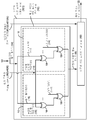
도 1은, 캐시 메모리에서 제공되는 예시적인 캐시 메모리 에러 검출 회로의 개략도이고, 여기서 캐시 메모리 에러 검출 회로는 캐시 메모리 상에서 수행되는 무효화 동작들 이후 캐시 메모리의 유효 표시자들에서 비트 플립들을 검출하도록 구성된다.
[0017]
도 2는 도 1의 캐시 메모리에서 일련의 예시적인 캐시 엔트리 이벤트들을 예시하는 표이고, 캐시 메모리 상에서 무효화 동작이 수행된 후 캐시 엔트리에 대한 유효 표시자에서 비트 플립의 발생, 및 인코딩된 여분의 정보 표시자를 이용하여 유효 표시자의 비트 플립을 검출하기 위한 도 1의 캐시 메모리 에러 검출 회로의 능력을 예시한다.
[0018]
도 3은, 캐시 메모리 상에서 수행되는 각각의 무효화 동작에 대해, 도 1의 캐시 메모리 에러 검출 회로의 무효화 인터벌 표시자에서 무효화 인터벌 상태를 진행시키기 위한 예시적인 프로세스를 예시하는 흐름도이다.
[0019]
도 4는, 캐시 메모리에서의 설정 시에 캐시 엔트리의 여분의 정보 표시자를 인코딩하기 위해 이용되는 무효화 인터벌 표시자로부터 현재의 무효화 인터벌 상태를 수신하는 도 1의 캐시 메모리 에러 검출 회로에서 여분의 정보 표시자 생성 회로의 예시적인 프로세스를 예시하는 흐름도이다.
[0020]
도 5는, 무효화 인터벌 표시자에서 현재의 무효화 인터벌 상태 및 액세스된 캐시 엔트리의 설정 동안 액세스된 캐시 엔트리로 인코딩된 여분의 정보 표시자에 기초하여 캐시 메모리의 액세스된 캐시 엔트리의 유효 표시자에서 비트 플립이 발생했는지 여부를 검출하는 도 1의 캐시 메모리 에러 검출 회로에서 여분의 정보 표시자 유효화 회로의 예시적인 프로세스를 예시하는 흐름도이다.
[0021]
도 6은, 캐시 메모리에서 제공되는 다른 예시적인 캐시 메모리 에러 검출 회로의 개략도이고, 여기서 캐시 메모리 에러 검출 회로는 캐시 메모리 상에서 수행되는 무효화 동작들 이후 캐시 메모리의 유효 표시자들에서 비트 플립들을 검출하도록 구성되고, 무효화 인터벌 표시자는 액세스된 캐시 엔트리에 대응하는 에러 검출 코드(예를 들어, 패리티)에서 인코딩된다.
[0022]
도 7은 도 6의 캐시 메모리에서 일련의 예시적인 캐시 엔트리 이벤트들을 예시하는 표이고, 캐시 메모리 상에서 무효화 동작이 수행된 후 캐시 엔트리에 대한 유효 표시자에서 비트 플립의 발생, 및 액세스된 캐시 엔트리의 에러 검출 코드의 일부로서 인코딩된 여분의 정보 표시자를 이용하여 유효 표시자의 비트 플립을 검출하기 위한 도 6의 캐시 메모리 에러 검출 회로의 능력을 예시한다.
[0023]
도 8은, 도 6의 캐시 메모리 에러 검출 회로에서 제공될 수 있는 예시적인 여분의 정보 표시자 유효화 회로의 개략도이고, 여기서 여분의 정보 표시자 유효화 회로는, 캐시 메모리의 캐시 엔트리의 설정 시에 무효화 인터벌 표시자로부터의 무효화 인터벌 상태로 인코딩되는 연관된 여분의 정보 표시자에 기초하여 액세스된 캐시 엔트리의 유효 표시자에서 비트 플립을 검출하도록 구성된다.
[0024]
도 9는, 도 6의 캐시 메모리 에러 검출 회로에서 제공될 수 있는 예시적인 여분의 정보 표시자 생성 회로의 개략도이고, 여기서 여분의 정보 표시자 생성 회로는, 액세스된 캐시 엔트리의 설정에서 무효화 인터벌 표시자로부터의 무효화 인터벌 상태 및 설정되는 액세스된 캐시 엔트리에 대응하는 인코딩된 에러 검출 코드에 기초하여 여분의 정보 표시자를 생성하도록 구성된다.
[0025]
도 10은, 캐시 메모리에서 설정된 캐시 엔트리의 에러 검출 코드의 일부로서 인코딩되는 무효화 인터벌 표시자로부터 현재의 무효화 인터벌 상태를 수신하는 도 9의 여분의 정보 표시자 생성 회로의 예시적인 프로세스를 예시하는 흐름도이다.
[0026]
도 11은, 무효화 인터벌 표시자에서 현재의 무효화 인터벌 상태 및 설정된 캐시 엔트리의 무효화 인터벌 상태로 인코딩되는 여분의 정보 표시자에 기초하여 캐시 메모리의 액세스된 캐시 엔트리의 유효 표시자에서 비트 플립이 발생했는지 여부를 검출하는 도 8의 여분의 정보 표시자 유효화 회로의 예시적인 프로세스를 예시하는 흐름도이다.
[0027]
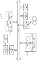
도 12는, 캐시 메모리의 캐시 엔트리들 상에서 수행되는 무효화 동작들 이후 캐시 메모리의 유효 표시자들에서 비트 플립들을 검출하도록 구성되는 임의의 캐시 메모리 에러 검출 회로를 포함하는 캐시 메모리를 포함할 수 있는 예시적인 프로세서-기반 시스템의 블록도이다.BRIEF DESCRIPTION OF THE DRAWINGS [0016] FIG. 1 is a schematic diagram of an exemplary cache memory error detection circuit provided in a cache memory, in which cache memory error detection circuitry includes bit flips in valid indicators of cache memory after invalidation operations performed on cache memory .
[0017] FIG. 2 is a table illustrating a series of exemplary cache entry events in the cache memory of FIG. 1, showing the occurrence of a bit flip in a valid indicator for a cache entry after an invalidate operation is performed on the cache memory, Illustrates the ability of the cache memory error detection circuit of Figure 1 to detect a bit flip of a valid indicator using an extra information indicator.
[0018] FIG. 3 is a flow chart illustrating an exemplary process for advancing the invalidation interval state in the invalidation interval indicator of the cache memory error detection circuit of FIG. 1 for each invalidation operation performed on the cache memory.
[0019] FIG. 4 is a block diagram of a cache memory error detection circuit of FIG. 1 that receives a current invalidation interval condition from a invalidation interval indicator used to encode an extra information indicator of a cache entry in a cache memory setting; Lt; RTI ID = 0.0 > flowchart < / RTI >
[0020] FIG. 5 is a graphical representation of an invalidation interval indicator in an invalidation interval indicator; a validation indication of the accessed cache entry in the cache memory based on the current invalidation interval state and an extra information indicator encoded in the cache entry accessed during the setting of the accessed cache entry; FIG. 2 is a flow chart illustrating an exemplary process of an extra information indicator validation circuit in the cache memory error detection circuit of FIG. 1 for detecting whether a bit flip has occurred in a register.
[0021] FIG. 6 is a schematic diagram of another exemplary cache memory error detection circuit provided in a cache memory, wherein the cache memory error detection circuit is operable, after the invalidation operations performed on the cache memory, And the invalidation interval indicator is encoded in an error detection code (e.g., parity) corresponding to the accessed cache entry.
[0022] FIG. 7 is a table illustrating a series of exemplary cache entry events in the cache memory of FIG. 6, showing the occurrence of a bit flip in a valid indicator for a cache entry after an invalidate operation has been performed on the cache memory, 6 illustrates the ability of the cache memory error detection circuitry of FIG. 6 to detect a bit flip of a valid indicator using an extra information indicator encoded as part of the error detection code of the cache entry.
[0023] FIG. 8 is a schematic diagram of an example redundant information indicator validation circuit that may be provided in the cache memory error detection circuit of FIG. 6, wherein the redundant information indicator validation circuit is configured to set the cache entry Is configured to detect a bit flip in a valid indicator of a cache entry accessed based on an associated redundant information indicator encoded in an invalidation interval state from an invalidation interval indicator.
[0024] FIG. 9 is a schematic diagram of an exemplary redundant information indicator generation circuit that may be provided in the cache memory error detection circuit of FIG. 6, wherein the redundant information indicator generation circuitry And to generate an extra information indicator based on the invalidation interval state from the invalidation interval indicator and the encoded error detection code corresponding to the accessed cache entry being set.
[0025] FIG. 10 illustrates an exemplary process of the redundant information indicator generation circuit of FIG. 9 that receives a current invalidation interval condition from an invalidation interval indicator encoded as part of an error detection code in a cache entry set in the cache memory Fig.
[0026] FIG. 11 illustrates an example of an invalidation interval indicator in an invalidation interval indicator, where the valid indicator of the accessed cache entry of the cache memory, based on the current invalidation interval state and the extra information indicator encoded in the invalidation interval state of the set cache entry, Fig. 8 is a flow chart illustrating an exemplary process of the redundant information indicator validation circuit of Fig.
[0027] Figure 12 includes a cache memory including any cache memory error detection circuitry configured to detect bit flips in valid indicators of cache memory following invalidation operations performed on cache entries of cache memory Gt; FIG. ≪ / RTI > is a block diagram of an exemplary processor-based system.
[0028] 본 명세서에 개시된 양상들은, 무효화 동작들에 후속하는 캐시 메모리의 유효 표시자들(예를 들어, 유효 비트들)에서의 비트 플립들을 검출하기 위한 캐시 메모리 에러 검출 회로들을 포함한다. 관련된 방법들 및 프로세서-기반 시스템들이 또한 개시된다. 무효화 동작 이후 그러나 캐시 엔트리가 재설정되기 전에 캐시 엔트리(예를 들어, 태그)에 대한 액세스로부터 캐시 히트가 얻어지면, 캐시 엔트리와 연관된 유효 표시자에서 비트 플립(들)이 발생하였다. 이것은, 무효화 동작 이후 캐시 엔트리의 재설정 전에는, 유효 표시자가 (캐시 히트에 대한) 유효 상태와는 반대로 (캐시 미스에 대한) 무효 상태를 표시해야 하기 때문이다. 따라서, 본 명세서에서 개시되는 양상들에서, 유효 표시자가 캐시 메모리의 액세스된 캐시 엔트리에 대해 유효 상태를 표시하는 경우, 캐시 메모리 에러 검출 회로가, 캐시 엔트리의 재설정 전에 캐시 엔트리에 대해 무효화 동작이 수행되었는지 여부를 결정하도록 구성된다. 캐시 엔트리에 대해 무효화 동작이 수행되었다면, 유효 표시자가 무효 상태를 표시해야 하기 때문에 유효 표시자에서 비트 플립이 발생하였고, 이는 캐시 미스가 생성되게 하거나 또는 에러가 표시되게 한다. 유효 표시자는 무효화 동작 이후 무효 상태로 설정되기 때문에, 유효 표시자는 무효 상태를 표시해야 한다. 캐시 메모리 에러 검출 회로는, 비트 플립(들)으로 인해 캐시 엔트리에 대한 유효 표시자가 유효 상태를 표시하는 경우에도, 결과적으로 캐시 미스가 생성되게 하거나 또는 액세스된 캐시 엔트리에 대해 에러가 표시되게 할 수 있다.[0028] Aspects disclosed herein include cache memory error detection circuits for detecting bit flips in valid indicators (e.g., significant bits) of a cache memory following invalidation operations. Related methods and processor-based systems are also disclosed. After the invalidation operation, however, if a cache hit is obtained from access to the cache entry (e.g., tag) before the cache entry is reset, the bit flip (s) has occurred in the validator associated with the cache entry. This is because the validator must indicate an invalid state (for cache misses) as opposed to a valid state (for cache hits) before the cache entry is reset after the invalidation operation. Thus, in aspects disclosed herein, if the valid indicator indicates a valid state for an accessed cache entry in the cache memory, the cache memory error detection circuit performs an invalidation operation on the cache entry before the cache entry is reset Or not. If an invalidation operation has been performed on the cache entry, a bit flip has occurred in the valid indicator because the valid indicator must indicate an invalid state, which causes a cache miss to be generated or an error to be displayed. Since the validator is set to the invalid state after the invalidation operation, the validator must indicate the invalid state. The cache memory error detection circuit may cause the cache miss to be generated or result in an error for the accessed cache entry even if the valid indicator for the cache entry indicates a valid state due to bit flip (s) have.
[0029]
이와 관련하여, 도 1은 캐시 메모리(12)에서 제공되는 예시적인 캐시 메모리 에러 검출 회로(10)의 개략도이다. 캐시 메모리(12)는 태그 어레이(14) 및 데이터 어레이(16)를 포함한다. 캐시 메모리(12)는 태그 어레이(14) 및 데이터 어레이(16)에서 캐시 엔트리들(18(0)-18(N))을 설정할 수 있고, 여기서 'N+1'은 캐시 메모리(12)에서 캐시 엔트리들(18)의 수이다. 캐시 엔트리들(18(0)-18(N))은 태그 어레이(14)에 연관된 태그(20(0)-20(N))를 저장함으로써 설정된다. 캐시 엔트리들(18(0)-18(N))의 설정은 또한 데이터 어레이(16)에 대응하는 데이터 엔트리들(22(0)-22(N))를 저장하는 것을 포함한다. 데이터 엔트리들(22(0)-22(N))은 상위 레벨 캐시 메모리 또는 메인 메모리와 같은 상위 레벨 메모리에 저장된 데이터에 대응할 수 있다. 캐시 엔트리(18(0)-18(N))의 설정 시에, 각각의 캐시 엔트리(18(0)-18(N))와 연관된 유효 표시자(24(0)-24(N))는, 캐시 엔트리(18(0)-18(N))의 유효성을 표시하는 유효 상태(예를 들어, 로직 하이 "1"을 저장함)로 설정된다. 캐시 엔트리(18(0)-18(N))가 더 이상 유효가 아니면, 더 이상 유효가 아닌 캐시 엔트리(18(0)-18(N))에 대해 대응하는 유효 표시자(24(0)-24(N))는 무효 상태(예를 들어, 로직 로우 "0"를 저장함)로 변경되어 캐시 엔트리(18(0)-18(N))를 무효화시킬 수 있다. 유효 표시자(24(0)-24(N))는 각각의 캐시 엔트리(18(0)-18(N))에 대해 캐시 미스 또는 다른 에러가 생성되어야 하는지 여부를 결정하기 위해 이용될 수 있다.[0029]
In this regard, FIG. 1 is a schematic diagram of an exemplary cache memory
[0030]
도 1을 계속 참조하면, 캐시 엔트리들(18(0)-18(N))의 캐시 엔트리(18)를 무효화하기를 원하는 경우, 무효화될 캐시 엔트리(18)에 대해 무효화 동작이 수행될 수 있다. 하나의 캐시 엔트리(18)가 무효화 동작에서 무효화될 수 있거나, 또는 전체 캐시 메모리(12) 또는 캐시 메모리의 다수의 캐시 엔트리들(18(0)-18(N))이 캐시 메모리(12) 상에서 수행되는 플래시 무효화 동작의 일부로서 무효화될 수 있다. 도 1의 캐시 메모리(12)의 캐시 엔트리들(18(0)-18(N)) 중 하나 이상에 대해 수행되는 무효화 동작은, 무효화 인에이블 입력(28) 상에서 수신되는 무효화 인에이블 신호(26)의 수신 시에 개시된다. 응답으로, 캐시 메모리(12)는 무효화되는 캐시 엔트리(18(0)-18(N))와 연관된 유효 표시자(24(0)-24(N))를 무효 상태로 설정한다. 모든 캐시 엔트리들(18(0)-18(N))을 무효화하기 위해 캐시 메모리(12) 상에서 플래시 무효화 동작이 수행되면, 캐시 메모리(12)는 모든 캐시 엔트리들(18(0)-18(N)))에 대응하는 모든 유효 표시자들(24(0)-24(N))의 상태를 무효 상태로 설정한다. [0030]
Continuing with FIG. 1, if it is desired to invalidate the
[0031]
도 1을 계속 참조하여, 캐시 엔트리(18(0)-18(N))에 대한 유효 표시자(24(0)-24(N))가 무효화 동작 이후 그러나 캐시 엔트리(18(0)-18(N))의 재설정 전에 유효 상태를 표시하면, 캐시 엔트리(18(0)-18(N))와 연관된 유효 표시자(24(0)-24(N))에서 비트 플립(들)이 발생한 것으로 공지된다. 이것은, 무효화 동작 이후 캐시 엔트리(18(0)-18(N))의 재설정 전에는, 유효 표시자(24(0)-24(N))가 (캐시 히트에 대한) 유효 상태와는 반대로 (캐시 미스에 대한) 무효 상태를 표시해야 하기 때문이다. 따라서, 유효 표시자(24(0)-24(N))가 캐시 메모리(12)의 액세스된 캐시 엔트리(18(0)-18(N))에 대한 유효 상태를 표시하는 경우, 아래에서 더 상세히 설명된 바와 같이, 캐시 메모리 에러 검출 회로(10)에 제공되는 여분의 정보 표시자 유효화 회로(30)는 캐시 엔트리(18(0)-18(N))의 재설정 전에 캐시 엔트리(18(0)-18(N)) 상에서 무효화 동작이 수행되었는지 여부를 결정할 수 있다. 캐시 엔트리(18(0)-18(N))의 재설정 전에 캐시 엔트리(18(0)-18(N))에 대해 무효화 동작이 수행되었다면, 캐시 엔트리(18(0)-18(N))에 대한 유효 표시자(24(0)-24(N))가 유효 표시자(24(0)-24(N))에서의 비트 플립(들)로 인해 유효 상태를 표시하더라도, 도 1의 캐시 메모리 에러 검출 회로(10)는 액세스되는 캐시 엔트리(18(0)-18(N))에 대해 캐시 미스가 생성되게 하거나 에러를 생성할 수 있다. [0031]
1, valid indicators 24 (0) -24 (N) for cache entries 18 (0) -18 (N) (0) -24 (N) associated with the cache entries 18 (0) -18 (N)) when the valid state is indicated before resetting the cache flags Lt; / RTI > This is because the validators 24 (0) -24 (N)) are in a state opposite to the valid state (for cache hits) before the reset of the cache entries 18 (0) Because of the invalidity state). Thus, if the valid indicators 24 (0) -24 (N) indicate the valid status for the accessed cache entries 18 (0) -18 (N) in the cache memory 12) The redundant information
[0032]
도 1을 계속 참조하여, 비트 플립이 발생한 것과 같이 액세스된 캐시 엔트리(18(0)-18(N))가 에러를 초래했는지 여부를 표시하기 위해, 캐시 엔트리 에러 표시자 라인(32) 상이 캐시 엔트리 에러 표시자(34)가 제공된다. 도 1에 도시된 일례로서, 캐시 엔트리 에러 표시자(34)는, 캐시 히트/미스 표시자 회로(38)에 대한 입력으로서 캐시 메모리 에러들(예를 들어, 패리티 에러들)을 표시하는 다른 선택적인 입력들(36)과 결합되어, 비제한적인 예로서 캐시 히트/미스 표시자 라인(42) 상의 캐시 히트/미스 표시자(40)를 생성할 수 있다. 다른 예로, 캐시 엔트리 에러 표시자(34)는, 캐시 에러 생성 및/또는 보고와는 별개로 액세스된 캐시 엔트리(18(0)-18(N))에 대한 유효 표시자(24(0)-24(N))에서 에러를 표시하기 위해 제공될 수 있다. 또 다른 예로, 캐시 엔트리 에러 표시자(34)는, 원하는 체크포인트를 리셋함으로써 역방향 에러 복원 또는 에러 정정 코드들(ECC)을 이용한 순방향 에러 복원을 생성하기 위해 이용될 수 있다.[0032]
With continued reference to Figure 1, the cache entry
[0033]
도 1의 캐시 메모리 에러 검출 회로(10)의 추가적인 예시적인 세부사항들을 논의하기 전에, 여기서 도 2는 먼저, 도 1의 캐시 메모리 에러 검출 회로(10)가 무효화 동작들 이후 유효 표시자들(24(0)-24(N))에서 비트 플립들을 어떻게 검출할 수 있는지를 기술하기 위해 설명된다. 이와 관련하여, 도 2는, 도 1의 캐시 메모리(12)의 캐시 엔트리(18(0))에 대해 수행되는 일련의 예시적인 이벤트들을 예시하는 표(44)를 예시한다. 그러나, 이 예는 또한 캐시 엔트리들(18(1)-18(N))에 액세스하는 것에도 적용됨을 주목해야 한다. 표(44)는, 무효화 동작 이후 캐시 엔트리(18(0))에 대한 유효 표시자(24(0))에서 비트 플립의 발생, 및 비트 플립을 검출하기 위한 도 1의 캐시 메모리 에러 검출 회로(10)의 능력을 예시한다. [0033]
Before discussing further exemplary details of the cache memory
[0034]
이와 관련하여, 도 1의 캐시 메모리(12)의 캐시 엔트리(18(0))를 예로 들면, 캐시 엔트리(18(0))는 도 2의 설정 이벤트(52)에 의해 캐시 메모리(12)에서 설명되는 것으로 도시된다. 유효 표시자(24(0))는 캐시 엔트리(18(0))의 설정 동안 유효 상태(예를 들어, "1")로 설정된다. 이 예에서 무효화 인터벌 카운트(48)의 형태인 현재의 무효화 인터벌 상태(예를 들어, "10")가 여분의 정보 표시자(46(0))로서 이용되고, 이는 설정 시에 캐시 엔트리(18(0))에 저장된다. 따라서, 이 실시예에서, 여분의 정보 표시자(46(0))는 무효화 인터벌 카운트(48)의 실제 코딩되지 않은 형태를 포함한다. 캐시 메모리 에러 검출 회로(10)는, 각각의 캐시 엔트리(18(0)-18(N))에 대응하는 여분의 정보 표시자(46(0)-46(N)) 및 이 예에서는 도 1의 캐시 메모리 에러 검출 회로(10)의 무효화 인터벌 카운터(50)의 형태인 무효화 인터벌 표시자에 의해 제공되는 현재 무효화 인터벌 카운트(48)를 이용하여 비트 플립을 검출한다. 태그(20(0))가 또한 캐시 엔트리(18(0))에 대해 설정된다. 무효화 인터벌 상태와는 상이한 상태들 또는 다른 상태들과 같이, 제한 없이 원하는 임의의 타입의 표시자를 저장하기 위해 카운터와는 상이한 다른 형태들로 무효화 인터벌 표시자가 제공될 수 있음을 주목한다.[0034]
In this regard, taking the cache entry 18 (0) of the cache memory 12 of FIG. 1 as an example, the cache entry 18 (0) is stored in the cache memory 12 And is illustrated as being described. The validity indicator 24 (0) is set to a valid state (e.g., "1 ") during the setting of the cache entry 18 (0). In this example, the current invalidation interval state (e.g., "10") in the form of an
[0035]
다음으로, 도 2를 계속 참조하면, 캐시 엔트리(18(0))에 대해 무효화 동작(54)이 수행된다. 무효화 동작(54)은 캐시 엔트리(18(0))에 대한 유효 표시자(24(0))의 유효 상태를, 앞서 논의된 바와 같이 캐시 엔트리(18(0))를 무효화하기 위한 무효 상태(예를 들어, "0")로 설정한다. 현재 무효화 인터벌 카운트(48)는 또한, 이 예에서는 무효화 동작(54)을 기록하기 위해 증분됨으로써 진행된다. 현재 무효화 인터벌 카운트(48)가 증분되었지만, 캐시 엔트리(18(0))의 여분의 정보 표시자(46(0))는 동일하게 유지됨을 주목한다. 이러한 정보는 추후에, 아래에서 설명되는 바와 같이, 캐시 엔트리(18(0))에 대한 이전의 설정 이벤트(52) 이후 무효화 동작(54)이 발생한 것을 결정하기 위해 이용된다. [0035]
2, invalidation operation 54 is performed on cache entry 18 (0). The invalidation operation 54 changes the validity status of the validity indicator 24 (0) for the cache entry 18 (0) to the invalidate status for invalidating the cache entry 18 (0) For example, "0"). The current
[0036]
도 2를 계속 참조하면, 이것은 다음으로, 방사 이벤트(56)가 발생하여, 이 예에서는 유효 표시자(24(0))에서 비트 플립(예를 들어, "0"으로부터 "1"로의 비트 플립)이 발생하게 하는 것을 예시하기 위해 가정된다. 그러나, 앞서 논의된 바와 같이, 캐시 엔트리(18(0))의 여분의 정보 표시자(46(0))는 현재 무효화 인터벌 카운트(48)와 동일하지 않고, 이는, 유효 표시자(24(0))가 무효 상태(예를 들어, '0')를 포함하는 것으로 예상되는 곳에서 무효화 동작(54)이 발생한 것을 의미한다. 따라서, 캐시 엔트리(18(0))가 재설정되기 전에 액세스 이벤트(58)에서 후속적으로 액세스되는 경우, 캐시 엔트리(18(0))에 대한 유효 표시자(24(0))는 유효 상태를 표시한다. 그러나, 앞서 언급된 바와 같이, 캐시 엔트리(18(0))는 이전의 무효화 동작(54)으로 인해 실제로는 유효가 아니다. 무효화 동작(54)의 결과로서 현재 무효화 인터벌 카운트(48)는 증분되었기 때문에, 현재 무효화 인터벌 카운트(48)는, 캐시 엔트리(18(0))가 설정된 때 캐시 엔트리(18(0))에 저장된 여분의 정보 표시자(46(0))에 매칭하지 않을 것이다. 따라서, 캐시 메모리 에러 검출 회로(10)는, 무효화 동작 (54) 이후 유효 표시자(24(0))에서 비트 플립이 발생한 것을 검출하기 위한 방법으로서 이러한 미스매치를 결정하도록 구성될 수 있다. 아래에서 더 상세히 논의될 바와 같이, 캐시 메모리 에러 검출 회로(10)는, 잘못된 캐시 히트가 생성되는 것을 방지하기 위해, 유효 표시자(24(0))가 비트 플립으로 인해 유효 상태를 표시하는 경우에도 캐시 엔트리(18(0))에 대한 액세스 이벤트(58)로 하여금 캐시 미스를 생성하거나 에러를 생성하게 할 수 있다.[0036]
Continuing with FIG. 2, this is followed by a spinning event 56 in which the bit flip (e. G., From "0" ) Is caused to occur. However, as discussed above, the extra information indicator 46 (0) of the cache entry 18 (0) is not the same as the current
[0037]
이와 관련하여, 도 1의 캐시 메모리 에러 검출 회로(10)의 더 예시적인 세부사항이 이제 논의될 것이다. 이와 관련하여, 도 1의 캐시 메모리 에러 검출 회로(10)의 여분의 정보 표시자 유효화 회로(30)는, 무효화 인터벌 카운터(50)에 기초하여, 캐시 엔트리(18(0)-18(N))의 재설정 전에 언제 무효화 동작(미도시)이 발생했는지를 결정한다. 무효화 인터벌 카운터(50)는, 이 예에서, 캐시 메모리(12)의 캐시 엔트리(18(0)-18(N)) 상에서 수행되는 각각의 무효화 동작에 대해 무효화 인터벌 카운트(48)를 증분시킨다. 무효화 인터벌 카운트(48)는, 캐시 엔트리(18(0)-18(N))가 캐시 메모리(12)에서 설정되는 경우 여분의 정보 표시자(46(0)-46(N))로서 여분의 정보 표시자 생성 회로(60)에 의해 캐시 엔트리(18(0)-18(N))에 저장된다. [0037]
In this regard, further exemplary details of the cache memory
[0038]
무효화 인터벌 카운터(50)는 무효화 인터벌 카운트(48)를 일(1)만큼 증분시키도록 구성될 수 있거나, 또는 무효화 인터벌 카운트(48)를 일(1)과는 다른 값들만큼 증분시키도록 요구될 수 있다. 무효화 인터벌 카운터(50)는 무효화 인터벌 카운터(50)에 의해 이용되는 비트들의 수에 기초하는 무효화 인터벌 카운트 값들의 범위에 걸쳐 무효화 인터벌 카운트(48)를 증분시키도록 구성될 수 있다. 예를 들어, 무효화 인터벌 카운터(50)에 의해 두개(2)의 비트들이 이용되면, 무효화 인터벌 카운트(48)에 대해 네개(4)의 가능한 값들(예를 들어, "00", "01", "10" 및 "11")이 존재할 것이고; 도 2에 설명되는 바와 같이, 세개(3)의 비트들은 여덟(8)개의 값들의 범위를 제공할 것이다. 또한, 무효화 인터벌 카운트(48)에 대한 무효화 인터벌 카운트 값들의 범위를 구성하는 것 또는 심지어 무효화 인터벌 구성 세팅(62)에 기초하여 무효화 인터벌 카운터(50)를 디스에이블시키는 것이 가능할 수 있다. 무효화 인터벌 카운트(48)는 무효화 인터벌 카운터(50)에 의해 여분의 정보 표시자 생성 회로(60) 및 또한 여분의 정보 표시자 유효화 회로(30)에 제공된다.[0038]
The invalidation interval counter 50 may be configured to increment the
[0039]
도 1을 계속 참조하여, 후속적으로 액세스되는 캐시 엔트리(18(0)-18(N))에 대한 유효 표시자(24(0)-24(N))가 유효 상태를 표시하면, 캐시 메모리 에러 검출 회로(10)의 여분의 정보 표시자 유효화 회로(30)는, 액세스되는 캐시 엔트리(18(0)-18(N))의 마지막 설정 이후 무효화 동작이 발생했는지 여부를 확인한다. 여분의 정보 표시자 유효화 회로(30)는, 현재 무효화 인터벌 카운트(48), 및 캐시 엔트리(18(0)-18(N))가 설정될 때 여분의 정보 표시자(46(0)-46(N))로서 캐시 엔트리(18(0)-18(N))에 저장된 무효화 인터벌 카운트에 기초하여 무효화 동작이 발생했는지 여부를 확인한다. 캐시 엔트리(18(0)-18(N))가 설정될 때 캐시 엔트리(18(0)-18(N))에 저장된 무효화 인터벌 카운트가, 액세스되는 캐시 엔트리(18(0)-18(N))에 대한 유효 표시자(24(0)-24(N))와 연관된 현재 무효화 인터벌 카운트(48)에 매칭하지 않으면, 이것은 미스매치를 초래한다. 이러한 미스매치는, 무효화 동작 이후 캐시 엔트리(18(0)-18(N))와 연관된 유효 표시자(24(0)-24(N))에서 비트 플립(들)이 발생했다는 표시이다. 이것은, 무효화 동작 이후, 액세스된 캐시 엔트리(18(0)-18(N))에 대한 유효 표시자(24(0)-24(N))가 유효 상태와는 반대로 무효 상태를 표시해야 하기 때문인데, 이는, 무효화 동작이 유효 표시자(24(0)-24(N))를 무효 상태로 강제하기 때문이다. [0039]
1, if the validators 24 (0) -24 (N) for the subsequently accessed cache entries 18 (0) -18 (N)) indicate a valid state, The redundant information
[0040]
따라서, 도 1의 이러한 예에서, 캐시 메모리 에러 검출 회로(10)의 여분의 정보 표시자 유효화 회로(30)는, 액세스되는 캐시 엔트리(18(0)-18(N))와 연관된 유효 표시자(24(0)-24(N))에서 비트 플립(들)이 검출되는 경우 (캐시 히트와는 반대로) 캐시 미스가 생성되게 하거나 에러를 생성하도록 구성된다. 캐시 엔트리(18(0)-18(N))와 연관된 여분의 정보 표시자(46(0)-46(N))에 매칭하지 않는 유효화 인터벌 카운터(50)에 의해 제공되는 현재 무효화 인터벌 카운트(48)는, 무효화 동작 이후 유효 카운터(24(0)-24(N))에서 비트 플립(들)이 발생했다는 표시이다. 검출된 무효화 동작 이후 비트 플립(들)이 검출되는 경우, 캐시 엔트리(18(0)-18(N))에 대응하는 데이터 어레이(16)에 저장된 데이터 엔트리(22(0)-22(N))를 이용하는 것을 회피하기 위해 캐시 미스 또는 다른 에러가 생성된다. 액세스된 캐시 엔트리(18(0)-18(N))에 대해 부정확한 유효 표시자(24(0)-24(N)) 상태가 검출되지 않았다면, 캐시 메모리(12)는 진정한 캐시 미스와는 반대로 잘못된 캐시 히트를 생성했을 것이다.[0040]
1, the redundant information
[0041]
이와 관련하여, 도 3은, 캐시 메모리(12)의 캐시 엔트리(18(0)-18(N)) 상에서 수행되는 각각의 무효화 동작(미도시)에 대해, 도 1의 캐시 메모리 에러 검출 회로(10)의 무효화 인터벌 카운터(50)에서 무효화 인터벌 카운트(48)를 증분시키기 위한 예시적인 프로세스를 예시하는 흐름도이다. 도 1 및 도 3을 참조하면, 무효화 인터벌 카운터(50)는 무효화 인에이블 신호(26)를 수신한다(블록(64)). 그 다음, 무효화 인터벌 카운터(50)는, 무효화 인에이블 신호(26)를 수신하는 것에 기초하여 무효화 인터벌 카운트(48)를 증분시킨다(블록(66)). 무효화 인터벌 카운터(50)는, 무효화 인터벌 구성 세팅(62)에 의해 설정되는 구성가능한 증분 양에 의해 무효화 인터벌 카운트(48)를 증분시킬 수 있다. 무효화 인터벌 카운터(50)는 또한, 무효화 인터벌 구성 세팅(62)에 기초하여 디스에이블되거나, 고정된 무효화 인터벌 카운트(48) 값으로 설정될 수 있다.[0041]
In this regard, FIG. 3 shows a cache memory error detection circuit (FIG. 1) for each invalidation operation (not shown) performed on the cache entries 18 (0) - 18 10 is a flowchart illustrating an exemplary process for incrementing the
[0042]
이와 관련하여, 도 4는, 설정 시에 캐시 엔트리(18(0)-18(N))에 여분의 정보 표시자(46(0)-46(N))를 저장하기 위해 무효화 인터벌 카운터(50)로부터 현재 무효화 인터벌 카운트(48)를 수신하는 도 1의 캐시 메모리 에러 검출 회로(10)에서 여분의 정보 표시자 생성 회로(60)의 예시적인 프로세스를 예시하는 흐름도이다. 도 1 및 도 4를 참조하면, 여분의 정보 표시자 생성 회로(60)는, 설정되는 캐시 엔트리(18(0)-18(N))에서 제공되는 태그(20(0)-20(N))를 수신하도록 구성된다(블록(68)). 여분의 정보 표시자 생성 회로(60)는 또한 무효화 인터벌 카운터(50)에 의해 제공되는 현재 무효화 인터벌 카운트(48)를 수신하도록 구성된다(블록(70)). 여분의 정보 표시자 생성 회로(60)는, 설정되는 캐시 엔트리(18(0)-18(N))의 무효화 인터벌 카운터(50)로부터 수신되는 현재 무효화 인터벌 카운트(48)를 저장한다(블록(72)). 이 예에서, 여분의 정보 표시자(46(0)-46(N))는 현재 무효화 인터벌 카운트(48)이고, 여분의 정보 표시자(46(0)-46(N))로서 캐시 엔트리(18(0)-18(N))에 저장된다. 여분의 정보 표시자(46(0)-46(N))는, 캐시 엔트리(18(0)-18(N))와 연관된 유효 표시자(24(0)-24(N))를 유효화하기 위해, 캐시 메모리 에러 검출 회로(10)의 여분의 정보 표시자 유효화 회로(30)에 의해 이용될 것이다.[0042]
In this regard, FIG. 4 shows an invalidation interval counter 50 (N) for storing redundant information indicators 46 (0) -46 (N) in the cache entries 18 (0) In the cache memory
[0043]
이와 관련하여, 도 5는, 캐시 메모리(12)의 액세스된 캐시 엔트리(18(0)-18(N))의 유효 표시자(24(0)-24(N))에서 비트 플립이 발생했는지 여부를 검출하는 도 1의 캐시 메모리 에러 검출 회로(10)에서 여분의 정보 표시자 유효화 회로(30)의 예시적인 프로세스를 예시하는 흐름도이다. 비트 플립이 발생했는지 여부를 검출하는 것은, 캐시 엔트리(18(0)-18(N))의 설정 동안 캐시 엔트리(18(0)-18(N))와 연관된 여분의 정보 표시자(46(0)-46(N))와 무효화 인터벌 카운터(50)의 현재 무효화 인터벌 카운트(48)를 비교하는 것에 기초한다. 도 1 및 도 5를 참조하면, 여분의 정보 표시자 유효화 회로(30)는, 캐시 엔트리(18(0)-18(N))에 저장된 여분의 정보 표시자(46(0)-46(N))에 기초하여 액세스되고 있는 캐시 엔트리(18(0)-18(N))에 대응하는 유효 표시자(24(0)-24(N))를 유효화한다. 여분의 정보 표시자 유효화 회로(30)는, 액세스된 캐시 엔트리(18(0)-18(N))에 대한 유효 표시자(24(0)-24(N))가 유효 상태를 표시하는 것에 대한 응답으로, 액세스되는 캐시 엔트리(18(0)-18(N))에 대한 여분의 정보 표시자(46(0)-46(N))를 수신한다(블록(74)). 여분의 정보 표시자 유효화 회로(30)는 또한 무효화 인터벌 카운터(50)로부터 현재 무효화 인터벌 카운트(48)를 수신한다(블록(76)). 여분의 정보 표시자 유효화 회로(30)는 액세스되는 캐시 엔트리(18(0)-18(N))와 연관된 여분의 정보 표시자(46(0)-46(N))를 현재 무효화 인터벌 카운트(48)와 비교한다(블록(78)). 현재 무효화 인터벌 카운트(48)가, 액세스된 캐시 엔트리(18(0)-18(N))에 대한 유효 표시자(24(0)-24(N))가 유효 상태를 표시한 때의 여분의 정보 표시자(46(0)-46(N))에 저장된 무효화 인터벌 값에 매칭하지 않으면, 이것은, 무효화 동작 이후 캐시 엔트리(18(0)-18(N))와 연관된 유효 표시자(24(0)-24(N))에서 비트 플립(들)이 발생했다는 표시이다. 이것은, 무효화 동작 이후, 액세스된 캐시 엔트리(18(0)-18(N))에 대한 유효 표시자(24(0)-24(N))가 유효 상태와는 반대로 무효 상태를 표시해야 하기 때문인데, 이는, 무효화 동작이 유효 표시자(24(0)-24(N))를 무효 상태로 강제하기 때문이다. 매칭은, 캐시 엔트리(18(0)-18(N))의 설정 및 설정된 캐시 엔트리(18(0)-18(N))의 액세스 둘 모두가 동일한 무효화 인터벌에서 발생했음을 표시할 것이다. 캐시 엔트리 에러 표시자(34)는, 여분의 정보 표시자(46(0)-46(N))와 현재 무효화 인터벌 카운트(48)와의 비교에 기초하여, 이러한 양상에서 액세스되는 캐시 엔트리(18(0)-18(N))에 대한 유효 표시자(24(0)-24(N))에서 비트 플립이 발생했는지 여부를 표시한다(블록(80)). [0043]
In this regard, FIG. 5 shows whether a bit flip occurred in the valid indicators 24 (0) - 24 (N) of the accessed cache entries 18 (0) - 18 And FIG. 3 is a flow chart illustrating an exemplary process of an extra information
[0044]
도 1의 캐시 메모리 에러 검출 회로(10)는, 방사 경화로 유효 표시자들(24(0)-24(N))을 보호하거나 캐시 엔트리(18(0)-18(N))에 대한 패리티와 같은 에러 검출 코드에 유효 표시자들(24(0)-24(N))을 포함함이 없이, 캐시 메모리(12)의 유효 표시자들(24(0)-24(N))에서 비트 플립(들)을 검출할 수 있다. 캐시 메모리 에러 검출 회로(10)는, 캐시 엔트리(18(0)-18(N))가 설정될 때 캐시 메모리(12)의 캐시 엔트리(18(0)-18(N))에 저장되는 무효화 인터벌 카운트(48)에 의해 비트 플립(들)을 검출할 수 있다. 캐시 엔트리(18(0)-18(N))에 대한 에러 검출 코드에 유효 표시자(24(0)-24(N))가 포함되면, 각각의 무효화된 캐시 엔트리(18(0)-18(N))의 에러 검출 코드는, 유효 표시자들(24(0)-24(N))을 무효 상태로 강제하는 것에 추가로 캐시 메모리 플래시 무효화 동작 시에 재계산되어, 플래시 무효화 동작의 레이턴시를 증가시켜야 할 것이다. 그러나, 설정 시에 각각의 캐시 엔트리(18(0)-18(N))에 무효화 인터벌 카운트(48)가 저장되면, 캐시 메모리(12)의 각각의 캐시 엔트리(18(0)-18(N))에 대해 추가적인 비트들이 포함되어야 한다. 캐시 엔트리(18(0)-18(N))가 설정될 때 무효화 인터벌 카운트(48)를 저장하기 위해 캐시 메모리(12)의 각각의 캐시 엔트리(18(0)-18(N))에 추가적인 비트들을 제공할 필요성을 회피하기 위해, 무효화 인터벌 카운트(48)는 대안적으로, 캐시 엔트리(18(0)-18(N))에 저장된 기존의 캐시 엔트리 에러 검출 코드(예를 들어, 패리티)와 인코딩될 수 있다. [0044]
The cache memory
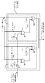
[0045]
이와 관련하여, 도 1과 유사한 캐시 엔트리 에러 검출을 제공하는 예시적인 캐시 메모리 에러 검출 회로(10(1))의 개략도가 도 6에 제공된다. 도 6의 캐시 메모리 에러 검출 회로(10(1))는, 공통 엘리먼트 번호들을 공유하는 도 1의 캐시 메모리 에러 검출 회로(10)와의 일부 공통 엘리먼트들을 포함한다. 따라서, 이러한 공통 엘리먼트들은 여기서 다시 설명되지 않을 것이다. 도 6의 캐시 메모리 에러 검출 회로(10(1))는 또한 캐시 엔트리(18(0)-18(N))에서 비트 플립(들)을 검출하는 기능을 제공한다. 캐시 메모리 에러 검출 회로(10(1))는, 도 1에서 앞서 설명된 적어도 하나의 무효화 인터벌 카운터(50(0)-50(M))로 이루어진다. 캐시 메모리 에러 검출 회로(10(1))는, 무효화 인터벌 카운트(48(0)-48(M))를 여분의 정보 표시자 생성 회로(60(1)) 및 또한 여분의 정보 표시자 유효화 회로(30(1)) 둘 모두에 제공한다. [0045]
In this regard, a schematic diagram of an exemplary cache memory error detection circuit 10 (1) that provides cache entry error detection similar to FIG. 1 is provided in FIG. The cache memory error detection circuit 10 (1) of FIG. 6 includes some common elements with the cache memory
[0046]
도 6을 계속 참조하면, 선택적인 무효화 동작들의 추적을 용이하게 하기 위해 연관된 무효화 인터벌 카운트들(48(0)-48(M))을 포함하는 복수의 무효화 인터벌 카운터들(50(0)-50(M))이 제공될 수 있다. 선택적인 무효화 동작은 캐시 엔트리들(18(0)-18(N))의 오직 일부에 대해서만 수행되는 무효화 동작이고, 그 일부는, 캐시 메모리(12(1))의 모든 캐시 엔트리들(18(0)-18(N))의 전부 또는 서브세트에 대해 수행되는 플래시 무효화 동작과는 반대로, 캐시 메모리(12(1))에서 인접할 수 있거나 인접하지 않을 수 있다. 선택적인 무효화 동작은, 인접할 수 있거나 인접하지 않을 수 있는 캐시 엔트리들(18(0)-18(N))의 서브세트가 특정 무효화 인터벌 카운터(50(0)-50(M)) 및 대응하는 무효화 인터벌 카운트(48(0)-48(M))와 연관되도록 허용한다. 선택적인 무효화 동작은, 특권, 보안, 예외 레벨, 상이한 동작 모드들, 엔트리들의 타입 등에 기초하여(그러나, 이에 제한되는 것은 아님) 결정될 수 있다. 이러한 방식으로, 도 6의 캐시 메모리 에러 검출 회로(10(1))는 무효화 인에이블 신호(26)에 대한 응답으로 캐시 엔트리들(18(0)-18(N))의 오직 일부와 연관된 무효화 인터벌 카운트(48(0)-48(M))를 증분시키도록 구성될 수 있다. [0046]
6, there is shown a plurality of invalidation interval counters 50 (0) -50 (0) - 50 (M)) including associated invalidation interval counts 48 (M) may be provided. The optional invalidation operation is an invalidation operation performed only on a part of the cache entries 18 (0) - 18 (N), and some of them are all cache entries 18 (1) May be contiguous or non-contiguous in the cache memory 12 (1), as opposed to a flash invalidation operation performed on all or a subset of the cache memory 12 (1) -18 (N). An optional invalidation operation is performed when a subset of cache entries 18 (0) -18 (N) that may or may not be contiguous) is associated with a particular invalidation interval counter 50 (0) -50 (M) To be associated with the invalidation interval counts 48 (0) - 48 (M). The optional invalidation actions may be determined based on (but not limited to) privileges, security, exception levels, different modes of operation, types of entries, and the like. In this manner, the cache memory error detection circuit 10 (1) of FIG. 6 is enabled to disable the invalidation enable
[0047]
도 6을 계속 참조하면, 캐시 메모리(12(1))는 이 예에서 복수의 데이터 어레이들(16(0)-16(X))을 포함하고, 데이터 어레이들(16)의 수는 "X+1"과 동일하다. 복수의 데이터 어레이들(16(0)-16(X)) 각각은 무효화 인터벌 카운터들(50(0)-50(M))과 연관된다. 복수의 데이터 어레이들(16(0)-16(X))이, 무효화 동작들이 기초할 수 있는 이벤트들의 공통 리스트, 예를 들어, 특권, 보안, 예외 레벨, 상이한 동작 모드, 엔트리들의 타입 등을 이용하고 있으면, 데이터 어레이들(16(0)-16(X))은 또한 공통 무효화 인터벌 카운터들(50(0)-50(M))을 공유한다. 복수의 캐시 메모리들(미도시)은 각각 여분의 정보 표시자 생성 회로(60(1)) 및 여분의 정보 표시자 유효화 회로(30(1))를 제공할 수 있다. 예를 들어, 복수의 캐시 메모리들(미도시)에 의해 제공되는 복수의 캐시 레벨들은 함께 무효화하여, 각각의 캐시 메모리(12(1)) 또는 캐시 메모리(12(1))의 각각의 레벨에 대한 무효화 인터벌 카운터(50(0)-50(M))에 대한 필요성을 제거할 수 있다. [0047]
6, the cache memory 12 (1) includes a plurality of data arrays 16 (0) -16 (X) in this example and the number of
[0048]
도 6을 계속 참조하면, 여분의 정보 표시자 생성 회로(60(1))는, 액세스되고 있는 캐시 엔트리(18(0)-18(N))와 연관된 무효화 인터벌 카운터(50(0)-50(M))에 의해 제공되는 현재 무효화 인터벌 카운트(48(0)-48(M))를 수신한다. 또한, 여분의 정보 표시자 생성 회로(60(1))는, 비제한적인 예로서, 태그 에러 검출 코드 생성 회로(84)에 의해 제공되는 제 2 입력으로서 태그 패리티(82)의 형태로 에러 검출 코드(81)를 수신한다. 태그 에러 검출 코드 생성 회로(84)는 캐시 엔트리(18(0)-18(N))에서 수신되는 태그(20(0)-20(N))에 기초하여 태그 패리티(82)를 생성한다. 태그 패리티(82)는, 태그(20(0)-20(N))가 손상되었는지 또는 그렇지 않으면 예상치 않게 변경되었는지 여부를 캐시 메모리(12(1))가 검출하도록 허용하는 에러 체크 목적으로 이용된다. 이 예에서, 여분의 정보 표시자 생성 회로(60(1))는 태그 패리티(82)를 수신하고, 수신된 무효화 인터벌 카운트(48(0)-48(M))를 인코딩하여, 태그 패리티(82)의 일부로서 수신된 무효화 인터벌 카운트(48(0)-48(M))의 인코딩된 버전을 제공한다. 이러한 인코딩의 결과로서, 여분의 정보 표시자 생성 회로(60(1))는, 설정되는 캐시 엔트리(18(0)-18(N))에 대응하는 저장될 여분의 정보 표시자(46'(1)(0)-46'(1)(N))의 인코딩된 버전을 출력한다. [0048]
6, the redundant information indicator generation circuit 60 (1) generates an invalidation interval counter 50 (0) -50 (N) associated with the cache entry 18 (0) (0) - 48 (M) provided by the current invalidation interval counts 48 (0) - 48 (M). The redundant information indicator generation circuit 60 (1) also includes, as a non-limiting example, error detection in the form of a
[0049]
태그 패리티(82)에서 무효화 인터벌 카운트(48(0)-48(M))를 인코딩하는 것은, 패리티 저장을 위한 추가적인 비트들의 필요성 없이 무효화 인터벌 카운트(48(0)-48(M))를 인코딩하는 이점을 허용한다. 이러한 형태의 인코딩은 또한, 유효 표시자(24(0)-24(N)) 및 태그(20(0)-20(N)) 에러 검출 코드(예를 들어, 패리티) 체크들을, 여분의 정보 표시자 유효화 회로(30(1))의 단일 동작으로 결합하는 이점을 제공한다. 그 다음, 저장된 인코딩된 여분의 정보 표시자(46'(1)(0)-46'(1)(N))는, 후속적으로 액세스되는 캐시 엔트리(18(0)-18(N))에 대응하는 유효 표시자(24(0)-24(N))를 유효화시키기 위해 이용된다. 그러나, 아래에서 더 상세히 논의되는 바와 같이, 도 6의 캐시 메모리(12(1))의 캐시 엔트리(18(0)-18(N))에서 비트 플립이 검출되면, 비트 플립은, 오직 유효 표시자(24(0)-24(N))에서와는 반대로, 캐시 엔트리(18(0)-18(N))의 어디에서든 발생할 수 있다.도 6의 캐시 메모리(12(1))를 추가로 설명하기 위해, 도 7은, 도 6의 캐시 메모리(12(1))에서 일련의 예시적인 캐시 엔트리(18(0)) 이벤트들을 예시하는 표(86)를 제공한다. 일례로, 표(86)는, 무효화 동작 이후 유효 표시자(24(0))에서 비트 플립의 발생, 및 인코딩된 여분의 정보 표시자(46'(1)(0)) 및 현재 무효화 인터벌 카운트(48(0))를 이용하여 캐시 엔트리(18(0)-18(N))에서 비트 플립을 검출하기 위한 능력을 예시한다. 도 7을 참조하면, 예시된 예시적인 이벤트들은 일련의 캐시 엔트리(18(0)) 이벤트들로 이루어진다. 캐시 엔트리(18(0))는 초기에 설정 이벤트(90)에서 설정된다. 캐시 엔트리(18(0))가 이벤트(90)를 설정할 때, 태그(20(0))는 태그 어레이(14)에 저장된다. 또한, 유효 표시자(24(0))는 캐시 메모리(12(1))에 의해 유효 상태(예를 들어, 로직 하이 또는 "1")로 설정된다. 이 예에서 여분의 정보 표시자(46(1)(0))는, 태그 어레이(14)의 캐시 엔트리(18(0))에 저장된 인코딩된 여분의 정보 표시자(46'(1)(0))를 제공하기 위해, 여분의 정보 표시자 생성 회로(60(1))에 의해 현재 무효화 인터벌 카운트(48(0))(예를 들어, "10")와 인코딩된다. 이 예에서, 여분의 정보 표시자 생성 회로(60(1))는, "배타적 or" 함수를 이용하여 태그(20(0))(예를 들어, "0111")와 현재 무효화 인터벌 카운트(48(0))(예를 들어, "10")를 인코딩하여, 캐시 엔트리(18(0))에 대응하여 저장된 "00"의 값을 도출한다. 어떤 시점에, 수신된 무효화 인에이블 신호(26)(미도시)에 의해 표시된 무효화 동작(92)은 적어도 하나의 캐시 엔트리(18(0))를 무효화한다. 무효화 동작(92)이 발생하는 경우, 캐시 메모리(12(1))는 유효 표시자(24(0))를 무효 상태(예를 들어, 로직 로우 또는 "0")로 설정할 것이다. 또한, 무효화 동작(92)을 표시하는 무효화 인에이블 신호(26)를 수신하는 것에 대한 응답으로, 현재 무효화 인터벌 카운트(48(0))은 무효화 인터벌 카운터(50(0))에 의해 구성된 인터벌에 의해 증분된다(예를 들어, "11"). 그러나, 현재 무효화 인터벌 카운트(48(0))이 증분되는 동안, 인코딩된 무효화 인터벌 카운트(48(0))와 저장된 인코딩된 여분의 정보 표시자(46'(1)(0))는 불변으로 남는다. [0049]
Encoding the invalidation interval counts 48 (0) -48 (M) in the
[0050] 도 7을 계속 참조하면, 캐시 메모리 에러 검출 회로(10(1))는 무효화 동작(92) 이후 캐시 엔트리(18(0)-18(N))에서 비트 플립들을 검출하도록 구성된다. 후속적으로 액세스되는 캐시 엔트리(18(0))에 대한 유효 표시자(24(0))가 유효 상태를 표시하면, 캐시 메모리 에러 검출 회로(10(1))는, 무효화 인터벌 카운터(50(0))에 의해 제공되는 현재 무효화 인터벌 카운트(48(0))의 인코딩된 버전이, 캐시 엔트리(18(0))가 설정될 때의 여분의 정보 표시자(46(1)(0))와 매칭하는 것을 확인한다. 현재 무효화 인터벌 카운트(48(0))는 여분의 정보 표시자(46(1)(0))와 동일한 방식으로 인코딩된다.따라서, 현재 무효화 인터벌 카운트(48(0))가 저장된 여분의 정보 표시자(46(1)(0))와 매칭하는 것은, 캐시 엔트리(18(0))를 설정하고 액세스하기 위해 동일한 무효화 인터벌 카운트(48(0))가 이용된 것을 의미한다. 따라서, 무효화 동작(92)은 캐시 엔트리(18(0))에 대한 액세스 전에 수행되지 않았다. 그러나, 캐시 엔트리(18(0))에 대한 액세스 이벤트(96) 시에, 현재 무효화 인터벌 카운트(48(0))의 인코딩된 버전은 캐시 엔트리(18(0))와 연관된 무효화 인터벌 카운트(48(0))와 매칭하지 않고, 이것은, 액세스된 캐시 엔트리(18(0))에 대한 유효 표시자(24(0))가 유효 상태를 표시하더라도 무효화 동작(92) 이후 액세스된 캐시 엔트리(18(0))에서 비트 플립(들)이 발생했다는 표시이다. 이러한 방식으로, 캐시 메모리(12(1))는 진정한 캐시 미스와는 반대로 잘못된 캐시 히트를 생성할 수 있다.[0050] 7, the cache memory error detection circuit 10 (1) is configured to detect bit flips in the cache entries 18 (0) - 18 (N) after the invalidation operation 92. If the valid indicator 24 (0) for the subsequently accessed cache entry 18 (0) indicates a valid state, the cache memory error detection circuit 10 (1) (0)) of the current invalidation interval count 48 (0) provided by the redundant information indicator 46 (1) (0) ≪ / RTI > The current invalidation interval count 48 (0) is encoded in the same manner as the redundant information indicator 46 (1) (0). Thus, the current invalidation interval count 48 (0) Matching the character 46 (1) (0) means that the same invalidation interval count 48 (0) is used to set and access the cache entry 18 (0). Thus, the invalidation operation 92 was not performed before accessing the cache entry 18 (0). However, in the access event 96 for the cache entry 18 (0), the encoded version of the current invalidation interval count 48 (0) includes the invalidation interval count 48 (0) associated with the cache entry 18 (0)), which means that even if the validator 24 (0) for the accessed cache entry 18 (0) indicates a valid state, it will not match the accessed cache entry 18 (0)) is an indication that the bit flip (s) has occurred. In this way, the cache memory 12 (1) may generate a false cache hit as opposed to a true cache miss.
[0051]
도 8은, 캐시 엔트리들(18(0)-18(N))에서 비트 플립들을 검출하기 위해 도 6의 캐시 메모리(12(1))의 캐시 메모리 에러 검출 회로(10(1))에서 제공될 수 있는 예시적인 여분의 정보 표시자 유효화 회로(30(1))의 개략적 도면의 추가적인 세부사항을 제공한다. 여분의 정보 표시자 유효화 회로(30(1))는, 캐시 엔트리(18(0)-18(N)) 설정 시에 무효화 인터벌 카운터(50(0)-50(M))로부터 무효화 인터벌 카운트(48(0)-48(M))와 인코딩되는 저장된 인코딩된 여분의 정보 표시자(46'(1)(0)-46'(1)(N))에 기초하여 캐시 엔트리(18(0)-18(N))에서 비트 플립을 검출하도록 구성된다. 도 8을 참조하면, 여분의 정보 표시자 유효화 회로(30(1))는 유효 표시자(24(0)-24(N))를 적절히 유효로 결정하기 위해, 저장된 인코딩된 여분의 정보 표시자(46'(1)(0)-46'(1)(N))를 현재 여분의 정보 표시자(98)와 비교하도록 구성된다. 현재 여분의 정보 표시자(98)의 생성은 아래에서 논의된다. 여분의 정보 표시자 비교 회로(100)는, 캐시 엔트리(18(0)-18(N)) 설정 시에 인코딩되는 인코딩된 여분의 정보 표시자(46'(1)(0)-46'(1)(N))를, 캐시 엔트리(18(0)-18(N)) 액세스 시에 생성된 현재 여분의 정보 표시자(98)와 비교하기 위해 제공된다. 인코딩된 여분의 정보 표시자들(46'(1)(0)-46'(1)(N)) 및 현재 여분의 정보 표시자(98)를 비교함으로써, 여분의 정보 표시자 유효화 회로(30(1))는, 캐시 엔트리(18(0)-18(N)) 설정에 후속하여 캐시 엔트리(18(0)-18(N)) 액세스 전에 무효화 동작이 발생했는지 여부를 결정할 수 있다. 인코딩된 여분의 정보 표시자들(46'(1)(0)-46'(1)(N)) 및 현재 여분의 정보 표시자(98)가 동일하지 않으면, 이것은, 캐시 엔트리(18(0)-18(N))의 설정 이후 무효화 동작이 발생했고, 연관된 유효 표시자(24(0)-24(N))는 무효 상태로 설정되어야 한다는 표시이다. [0051]
8 is a block diagram of the cache memory error detection circuit 10 (1) of the cache memory 12 (1) of FIG. 6 for detecting bit flips in the cache entries 18 (0) - 18 Which provides additional details of a schematic drawing of an exemplary redundant information indicator validation circuit 30 (1) that may be used. The extra information indicator validation circuit 30 (1) acquires the invalidation interval count ((0)) from the invalidation interval counter 50 (0) -50 (M) at the time of setting the cache entry 18 (0) -46 '(1) (N) based on the stored encoded extra information indicator 46' (1) (0) -46 '(1) (N) -18 (N)). ≪ / RTI > 8, the redundant information indicator validation circuit 30 (1) is configured to validate the valid indicator 24 (0) - 24 (N) (1) (0) -46 '(1) (N) to the current redundant information indicator 98. The generation of the current extra information indicator 98 is discussed below. The redundant information
[0052]
도 8을 계속 참조하면, 현재 여분의 정보 표시자(98)는, 여분의 정보 표시자 유효화 회로(30(1))에 제공되는 제 2 여분의 정보 표시자 생성 회로(102)에 의해 생성된다. 제 2 여분의 정보 표시자 생성 회로(102)는, 비제한적인 예로서, 도 6의 태그 에러 검출 코드 회로(106)에 의해 제공되는 태그 패리티(104)의 형태로 현재 생성된 에러 검출 코드(103)를 수신한다. 제 2 여분의 정보 표시자 생성 회로(102)는 또한 무효화 인터벌 카운터(50(0)-50(M))에 의해 제공되는 현재 무효화 인터벌 카운트(48(0)-48(M))를 수신한다. 무효화 인터벌 카운트(48(0)-48(M))는 캐시 엔트리(18(0)-18(N)) 액세스 시에 현재 무효화 인터벌 카운트(48(0)-48(M))를 표현한다. 현재 여분의 정보 표시자(98)는 인코딩된 여분의 정보 표시자(46'(1)(0)-46'(1)(N))와 유사한 방식으로 제 2 여분의 정보 표시자 생성 회로(102)에 의해 생성된다. [0052]
8, the current extra information indicator 98 is generated by the second spare information
[0053]
도 8을 계속 참조하면, 제 2 여분의 정보 표시자 생성 회로(102)는 현재 여분의 정보 표시자(98)를 생성하기 위해 OR-기반 함수를 구현하는 복수의 로직 게이트들(108)을 이용한다. 예를 들어, 로직 게이트들(108)은 이 예에서 XOR 게이트들이지만, OR-기반 게이트들, 예를 들어, OR 및/또는 NOR 게이트들을 포함하는 다른 게이트들이 또한 예시들로서 이용될 수 있다. 비제한적인 예로서, 무효화 인터벌 카운트(48(0)-48(M))가 "10"이고 태그(20(0)-20(N))가 "0111"이면, 제 1 패리티 생성 회로(110)는 "10" + "0111" 또는 "100111"의 결합된 또는 연접된 값의 홀수번째 비트들에 대해 "배타적 or" 함수를 수행한다. 결합된 또는 연접된 값 "100111"의 처음 두개(2)의 비트들은 무효화 인터벌 카운트(48(0)-48(M))이고, 두번째 네개(4)의 비트들은 캐시 엔트리(18(0)-18(N))의 태그(20(0)-20(N))이다. 결합된 또는 연접된 값 "100111"의 홀수번째 비트들에 대한 "배타적 or" 함수의 결과들은 "0"이고, 이는 인코딩된 여분의 정보 표시자(46'(1)(0)-46'(1)(N))의 제 1 비트가 된다. 제 2 패리티 생성 회로(112)에서, 태그 패리티(104)의 짝수번째 비트들 및 무효화 인터벌 카운트(48(0)-48(M))의 짝수번째 비트들은, 짝수번째 비트들 각각에 적용되는 동일한 "배타적 or" 함수를 이용하여 인코딩된다. 결과는 인코딩된 여분의 정보 표시자(46'(1)(0)-46'(1)(N))의 제 2 비트를 형성한다. 결과적 인코딩된 여분의 정보 표시자(46'(1)(0)-46'(1)(N))는 홀수번째 및 짝수번째 비트들 각각에 적용되는 "배타적 or" 함수를 통해 무효화 인터벌 카운트(48(0)-48(M))와 인코딩된 태그 패리티(104)가 된다. "배타적 or" 함수 이외에 다른 디지털 로직 함수들이 이용될 수 있음을 주목해야 한다. [0053]
8, the second redundant information
[0054]
도 6 및 도 8을 계속 참조하면, 여분의 정보 표시자 유효화 회로(30(1))는, 태그 패리티[0]과 같은 태그 패리티(104)를 표현하는 복수의 비트들을 수신하도록 구성될 수 있다. 114는 제 1 또는 최하위 비트 및 태그 패리티[Y]를 표현한다. 116은 마지막 또는 최상위 비트를 표현하고, 여기서 태그 패리티(104)에는 Y개의 비트들이 존재한다. 여분의 정보 표시자 유효화 회로(30(1))는 또한, 무효화 인터벌 카운트[0]과 같은 무효화 인터벌 카운트(48(0)-48(M))를 표현하는 복수의 비트들을 수신하도록 구성될 수 있다. 118은 제 1 또는 최하위 비트 및 무효화 인터벌 카운트[Z]를 표현한다. 120은 마지막 또는 최상위 비트를 표현하고, 여기서 무효화 인터벌 카운트(48(0)-48(M))에는 Z개의 비트들이 존재한다. 결과적 인코딩된 여분의 정보 표시자(46'(1)(0)-46'(1)(N))는, 캐시 엔트리(18(0)-18(N))에 대응하는 태그 어레이(14)에 저장된다.[0054]
6 and 8, the redundant information indicator validation circuit 30 (1) may be configured to receive a plurality of bits representing
[0055]
생성되면, 현재 여분의 정보 표시자(98)는, 매치가 존재하는지 여부를 결정하기 위해 여분의 정보 표시자 비교 회로(100)에 의해 저장된 인코딩된 여분의 정보 표시자(46'(1)(0)-46'(1)(N))와 비교된다. 매치가 존재하면, 이것은, 동일한 무효화 인터벌 카운트(48(0)-48(M))에 의해 표현되는 바와 같이 캐시 엔트리(18(0)-18(N)) 설정 및 캐시 엔트리(18(0)-18(N) 액세스가 동일한 무효화 인터벌에서 발생한 이후 유효 표시자(24(0)-24(N))가 유효여야 한다는 표시이다. 비교의 결과로서, 여분의 정보 표시자 비교 회로(100)는, 캐시 엔트리(18(0)-18(N))에서 비트 플립(들)이 발생했는지 여부를 시그널링하는 캐시 엔트리 에러 표시자(122)를 생성한다.[0055]
Once created, the current redundant information indicator 98 may include a redundant information indicator 46 '(1) (stored) by the redundant information
[0056]
도 6을 계속 참조하면, 캐시 메모리(12(1))의 예시적인 여분의 정보 표시자 생성 회로(60(1))의 개략도의 추가적인 세부사항이 도 9에 제공된다. 여분의 정보 표시자 생성 회로(60(1))는, 캐시 엔트리(18(0)-18(N))가 설정될 때 무효화 인터벌 카운트(48(0)-48(M)) 및 설정되는 캐시 엔트리(18(0)-18(N))에 대응하는 인코딩된 에러 검출 코드(예를 들어, 패리티)에 기초하여, 인코딩된 여분의 정보 표시자(46'(1)(0)-46'(1)(N))를 생성하도록 구성된다. 도 9의 여분의 정보 표시자 생성 회로(60(1))를 참조하면, 인코딩된 여분의 정보 표시자(46'(1)(0)-46'(1)(N))를 생성하기 위해 태그 패리티(82)와 무효화 인터벌 카운트(48(0)-48(M))를 인코딩하는 하나의 방법이 예시된다. 이 예에서, 여분의 정보 표시자 생성 회로(60(1))는 태그 패리티(82)에서 무효화 인터벌 카운트(48(0)-48(M))를 인코딩하기 위해 "배타적 or" 함수를 구현하는 복수의 로직 게이트들(108)을 이용한다. 여분의 정보 표시자 생성 회로(60(1))는 여분의 정보 표시자 유효화 회로(30(1))와 유사하다. "배타적 or" 함수는 디지털 회로들에서 에러 검출 코드로서 패리티 생성을 구현하기 위해 이용될 수 있다. 이 예에서, 여분의 정보 표시자 생성 회로(60(1))는, 수신된 입력들의 홀수번째 및 짝수번째 비트들 각각에 "배타적 or"를 적용하는 것에 기초하여, 인코딩된 여분의 정보 표시자(46'(1)(0)-46'(1)(N))를 생성할 것이다. 제 1 패리티 생성 회로(110)에서, 태그 패리티(82)의 홀수번째 비트들 및 무효화 인터벌 카운트(48(0)-48(M))의 홀수번째 비트들은, 홀수번째 비트들 각각에 적용되는 "배타적 or" 함수를 이용하여 인코딩된다. 결과는 인코딩된 여분의 정보 표시자(46'(1)(0)-46'(1)(N))의 제 1 비트를 형성한다. [0056]
6, additional details of a schematic diagram of an exemplary redundant information indicator generation circuit 60 (1) of cache memory 12 (1) is provided in FIG. The redundant information indicator generation circuit 60 (1) generates the invalidation interval counts 48 (0) to 48 (M) and the set cache (not shown) when the cache entries 18 (0) (0) -46 ') based on the encoded error detection code (e.g., parity) corresponding to the entry 18 (0) -18 (N) (1) (N). Referring to the redundant information indicator generation circuit 60 (1) of FIG. 9, it is possible to generate the redundant information indicator 46 '(1) (0) -46' (1) One way to encode the
[0057]
도 6과 관련하여 도 9를 계속 참조하면, 비제한적인 예로서, 무효화 인터벌 카운트(48(0)-48(M))가 "10"이고 태그(20(0)-20(N))가 "0111"이면, 제 1 패리티 생성 회로(110)는 "10" + "0111" 또는 "100111"의 결합된 또는 연접된 값의 홀수번째 비트들에 대해 "배타적 or" 함수를 수행한다. 결합된 또는 연접된 값 "100111"의 처음 두개(2)의 비트들은 무효화 인터벌 카운트(48(0)-48(M))이고, 두번째 네개(4)의 비트들은 캐시 엔트리(18(0)-18(N))의 태그(20(0)-20(N))이다. 결합된 또는 연접된 값 "100111"의 홀수번째 비트들에 대한 "배타적 or" 함수의 결과들은 "0"이고, 이는 인코딩된 여분의 정보 표시자(46'(1)(0)-46'(1)(N))의 제 1 비트가 된다. 제 2 패리티 생성 회로(112)에서, 태그 패리티(82)의 짝수번째 비트들 및 무효화 인터벌 카운트(48(0)-48(M))의 짝수번째 비트들은, 짝수번째 비트들 각각에 적용되는 동일한 "배타적 or" 함수를 이용하여 인코딩된다. 결과는 인코딩된 여분의 정보 표시자(46'(1)(0)-46'(1)(N))의 제 2 비트를 형성한다. 결과적 인코딩된 여분의 정보 표시자(46'(1)(0)-46'(1)(N))는 홀수번째 및 짝수번째 비트들 각각에 적용되는 "배타적 or" 함수를 통해 무효화 인터벌 카운트(48(0)-48(M))와 인코딩된 태그 패리티(82)가 된다. "배타적 or" 함수 이외에 다른 디지털 로직 함수들이 이용될 수 있음을 주목해야 한다.[0057]
Continuing with Fig. 9 with reference to Fig. 6, a non-limiting example is shown where the invalidation interval counts 48 (0) -48 (M) are "10 & 0111 ", the first
[0058]
도 6 및 도 9를 계속 참조하면, 여분의 정보 표시자 생성 회로(60(1))는, 태그 패리티[0]과 같은 태그 패리티(82)를 표현하는 복수의 비트들을 수신하도록 구성될 수 있다. 114는 제 1 또는 최하위 비트 및 태그 패리티[Y]를 표현한다. 116은 마지막 또는 최상위 비트를 표현하고, 여기서 태그 패리티(82)에는 Y개의 비트들이 존재한다. 여분의 정보 표시자 생성 회로(60(1))는 또한, 무효화 인터벌 카운트[0]과 같은 무효화 인터벌 카운트(48(0)-48(M))를 표현하는 복수의 비트들을 수신하도록 구성될 수 있다. 118은 제 1 또는 최하위 비트 및 무효화 인터벌 카운트[Z]를 표현한다. 120은 마지막 또는 최상위 비트를 표현하고, 여기서 무효화 인터벌 카운트(48(0)-48(M))에는 Z개의 비트들이 존재한다. 결과적 인코딩된 여분의 정보 표시자(46'(1)(0)-46'(1)(N))는, 캐시 엔트리(18(0)-18(N))에 대응하는 태그 어레이(14)에 저장된다.[0058]
6 and 9, redundant information indicator generation circuit 60 (1) may be configured to receive a plurality of bits representing
[0059]
도 6을 계속 참조하면, 여분의 정보 표시자 유효화 회로(30(1))는, 액세스되고 있는 캐시 엔트리(18(0)-18(N))에 대한 응답으로, 현재 무효화 인터벌 카운트(48(0)-48(M))를 수신하도록 구성된다. 여분의 정보 표시자 유효화 회로(30(1))는 또한, 액세스되는 캐시 엔트리(18(0)-18(N))에 대응하여 저장되는 인코딩된 여분의 정보 표시자(46'(1)(0)-46'(1)(N))를 수신하도록 구성된다. 추가적으로, 여분의 정보 표시자 유효화 회로(30(1))는 태그 패리티 회로(106)로부터 현재 생성된 태그 패리티(104)를 수신하도록 구성된다. 현재 생성된 태그 패리티(104)는 앞서 논의된 태그 패리티 생성 회로(84)로부터 생성되는 태그 패리티(82)와 유사한 방식으로 생성된다. 태그 패리티 회로(106)는 태그 패리티 회로(106)에 제공되는 로직 게이트들(미도시)을 이용하여 현재 생성된 태그 패리티(104)를 생성한다. 그러나, 이 예에서, 태그 패리티(104)를 체크하는 것은 태그 패리티 회로(106)에서 수행되지 않는다. 이 예에서, 태그 패리티(104)는 여분의 정보 표시자 유효화 회로(30(1))에서 체크된다. 태그 패리티(104)가 여전히 체크되지만, 이것은 이제, 인코딩된 여분의 정보 표시자(46'(1)(0)-46'(1)(N))에 대해 동일한 수의 비트들이 여전히 이용되더라도, 태그(20(0)-20(N)) 및 유효 표시자(24(0)-24(N)) 둘 모두에 대해 수행된다. 인코딩된 여분의 정보 표시자(46'(1)(0)-46'(1)(N))에 대해, 오직 태그(20(0)-20(N))에 대한 태그 패리티(104) 체크만이 수행되는 시나리오에서 이용될 수와 동일한 수의 비트들이 이용된다. 이러한 방식으로, 인코딩된 여분의 정보 표시자(46'(1)(0)-46'(1)(N))는 유효 표시자(24(0)-24(N)) 및 또한 태그(20(0)-20(N)) 둘 모두에 대해 에러 검출 코드(예를 들어, 패리티) 보호를 제공한다. 추가적으로, 무효화 인터벌 카운터(50(0)-50(M))는 또한 무효화 동작들을 추적하기 위해 다른 캐시 메모리들(미도시)에 의해 이용될 수 있다. [0059]
6, the redundant information indicator validation circuit 30 (1) determines whether or not the current invalidation interval count 48 (N) is in response to the cache entry 18 (0) - 18 0) -48 (M). The redundant information indicator validation circuit 30 (1) also includes an encoded extra information indicator 46 '(1) ((N)) stored in correspondence with the accessed
[0060]
하나의 비제한적인 예로서, 도 6의 캐시 메모리 에러 검출 회로(10(1))의 각각의 무효화 인터벌 카운트(48(0)-48(M))에서 제공되는 비트들의 수는 태그 패리티(82)의 비트들의 수보다 적거나 그와 동일하게 제공될 수 있다. 그렇지 않으면, 도 8의 여분의 정보 표시자 유효화 회로(30(1))가 모든 시나리오들에서 비트 플립들을 검출하는 것이 가능하지는 않을 수 있다. 예를 들어, 무효화 인터벌 카운트(48)에서 제공된 네개(4)의 카운터 비트들 및 현재의 태그 패리티(104)에서 제공된 두개(2)의 패리티 비트들이 존재한다고 가정한다. 또한, '0111' 및 '1000'의 카운터 값들을 무효화 인터벌 카운트들(48)로서 가정한다. '0111' 및 '1000'의 이러한 무효화 인터벌 카운트들의 짝수번째 및 홀수번째 비트들이 고려되는 경우, 둘 모두는, 도 9의 여분의 정보 표시자 생성 회로(60(1))에 의해 동일한 "짝수" 결과 = 1 XOR 1 = 0 XOR 0 = 0가 생성되는 것을 도출한다. 둘 모두는 또한, 도 9의 여분의 정보 표시자 생성 회로(60(1))에 의해 동일한 "홀수" 결과 = 0 XOR 1 = 1 XOR 0 = 1이 생성되는 것을 도출한다. 따라서, 무효화 인터벌 카운트(48)가 무효화 동작으로 인해 '0111'로부터 '1000'으로 증분되는 경우, 여분의 정보 표시자 생성 회로(60(1))는 새로운 무효화 인터벌 카운트(48)로서 '0111' 및 '1000'의 무효화 인터벌 카운트들 둘 모두에 대한 인코딩된 여분의 정보 표시자(46')에서 동일한 값을 인코딩한다. 따라서, 이 예에서, '0111'로부터 '1000'으로 무효화 인터벌 카운트(48)를 증분시키는 대응하는 무효화 동작 이후, 도 8의 여분의 정보 표시자 유효화 회로(30(1))가 비트 플립을 검출하는 것이 가능하지 않을 것인데, 이는, 여분의 정보 표시자 생성 회로(60(1))에 의해 제공되는 여분의 정보 표시자(46)의 인코딩 결과들이 이 예에서는 동일할 것이기 때문이다. [0060]
As one non-limiting example, the number of bits provided in each invalidation interval count 48 (0) -48 (M) of the cache memory error detection circuit 10 (1) ) ≪ / RTI > Otherwise, the redundant information indicator validation circuit 30 (1) of FIG. 8 may not be able to detect bit flips in all scenarios. For example, assume that there are four (4) counter bits provided in the
[0061]
또한, 캐시 엔트리들(18(0)-18(N))을 설정하는 경우, 여분의 정보 표시자(46(1)(0)-46(1)(N))는 현재 무효화 인터벌 카운트(48(0)-48(M))와는 상이한 인코딩된 여분의 정보 표시자(46')를 제공하기 위해 무효화 인터벌 카운트와 인코딩될 수 있는 것이 가능함을 주목한다. 이 기술은, 플래시 무효화들이 아닌 캐시 메모리(12(1)) 상에서 수행되는 다른 동작들에 대해 이용될 수 있다. 예를 들어, 특정 캐시 엔트리(18(0)-18(N))를 무효로 타겟팅하는 것이 요구될 수 있다. 이 예에서, 타겟팅된 캐시 엔트리(18(0)-18(N))에 대한 유효 표시자(24(0)-24(N))는, 대응하는 캐시 엔트리(18(0)-18(N))가 무효인 것을 표시하는 무효 표시자로 오버라이트될 수 있다. 타겟팅된 캐시 엔트리(18(0)-18(N))에 대한 태그 패리티(82)가 또한 오버라이트될 수 있다. 이러한 방식으로, 유효 표시자(24(0)-24(N))가 유효 상태로 다시 플립하면, 이것은 검출될 수 있다. 현재 무효화 인터벌 카운트(48(0)-48(M))는 또한 증분되지 않을 것이다. 이러한 방식으로, 무효화 동작들 이후 다른 설정된 캐시 엔트리들(18(0)-18(N))에서 비트 플립들을 검출하기 위한 캐시 메모리(12(1))의 능력은 영향받지 않는데, 이는, 다른 설정된 캐시 엔트리들(18(0)-18(N))에 대한 태그 패리티(82)를 인코딩하기 위해 이용된 현재 무효화 인터벌 카운트(48(0)-48(M))가 변경되지 않기 때문이다.[0061]
In addition, when setting the cache entries 18 (0) - 18 (N), the redundant information indicator 46 (1) (0) -46 (1) (N) Note that it is possible to be encoded with the invalidation interval count to provide an encoded extra information indicator 46 'that is different than the encoded information indicator 46' (0) -48 (M). This technique may be used for other operations performed on the cache memory 12 (1) rather than flash invalidations. For example, it may be required to invalidate a particular cache entry 18 (0) - 18 (N). In this example, the valid indicators 24 (0) -24 (N) for the targeted cache entries 18 (0) -18 (N)) are associated with the corresponding cache entries 18 ) May be overwritten with an invalid indicator indicating that it is invalid. The
[0062]
이 예에서, 인코딩된 여분의 정보 표시자(46'(1)(0)-46'(1)(N))를 제공하기 위해, 현재 무효화 인터벌 카운트(48(0)-48(M))와는 상이한 무효화 인터벌 카운트가, 타겟팅된 캐시 엔트리(18(0)-18(N))에 대응하는 여분의 정보 표시자(46(1)(0)-46(1)(N))를 인코딩하는데 이용될 수 있다. 예를 들어, 타겟팅된 캐시 엔트리(18(0)-18(N))에 대응하는 인코딩된 여분의 정보 표시자(46'(1)(0)-46'(1)(N))를 인코딩하기 위해, 현재 무효화 인터벌 카운트(48)에 대해 구성된 카운트 값들의 범위 밖에 있는 무효화 인터벌 카운트가 이용될 수 있다. 그렇지 않고, 무효화 동작이 무효화 인에이블 신호(26)를 시그널링하는 타입이 아니고, 따라서 현재 무효화 인터벌 카운트(48(0)-48(M))를 진행시키지 않으면, 무효화된 타겟팅된 캐시 엔트리(18(0)-18(N))에 대해 유효 표시자(24(0)-24(N))에서 발생하는 비트 플립은 여분의 정보 표시자 유효화 회로(30(1))에 의해 검출되지 않을 수 있다.[0062]
In this example, the current invalidation interval counts 48 (0) -48 (M)) to provide the encoded extra information indicators 46 '(1) (0) -46' (1) (0) -46 (1) (N) corresponding to the targeted cache entries 18 (0) - 18 (N)), which are different from the invalidation interval counts Can be used. (1) (0) -46 '(1) (N)) corresponding to the targeted cache entries 18 (0) -18 (N) An invalidation interval count that is outside the range of count values configured for the current
[0063]
도 10과 관련하여, 설정되는 캐시 엔트리(18(0)-18(N))의 태그 패리티(82)에서 인코딩하기 위해 무효화 인터벌 카운터(50(0)-50(M))로부터 현재 무효화 인터벌 카운트(48(0)-48(M))를 수신하는 도 6의 여분의 정보 표시자 생성 회로(60(1))의 예시적인 프로세스를 예시하는 흐름도가 제공된다. 여분의 정보 표시자 생성 회로(60(1))는, 설정되는 캐시 엔트리(18(0)-18(N))에 기초하여 태그 패리티(82)를 수신하도록 구성된다(블록(124)). 태그 패리티(82)는 태그 에러 검출 코드 생성 회로(84)에 의해 에러 검출 코드(81)로서 생성된다. 또한, 여분의 정보 표시자 생성 회로(60(1))는 현재 무효화 인터벌 카운트(48(0)-48(M))를 수신하도록 구성된다(블록(126)). 여분의 정보 표시자 생성 회로(60(1))는, 캐시 엔트리(18(0)-18(N))를 설정하는 것에 대한 응답으로, 현재 무효화 인터벌 카운트(48(0)-48(M))에 기초하여 캐시 엔트리들(18(0)-18(N)) 각각에 대한 인코딩된 여분의 정보 표시자(46'(1)(0)-46'(1)(N))를 제공하도록 구성된다(블록(128)). 이 예에서, 앞서 설명된 바와 같이, 인코딩은 도 6 및 도 9에서 설명된 바와 같이 태그 패리티(82)와 무효 인터벌 카운트(48(0)-48(M))를 인코딩하기 위해 "배타적 or" 함수를 이용하는 것을 포함한다. 인코딩되면, 캐시 엔트리들(18(0)-18(N)) 각각에 대한 인코딩된 여분의 정보 표시자(46'(1)(0)-46'(1)(N))는, 캐시 엔트리들(18(0)-18(N)) 각각에 대응하는 태그 어레이(14)에 저장된다(블록(130)). 저장된 인코딩된 여분의 정보 표시자(46'(1)(0)-46'(1)(N))는 유효 표시자(24(0)-24(N))에서 비트 플립을 검출하기 위해 여분의 정보 표시자 유효화 회로(30(1))에 의해 이용될 것이다.[0063]
10, from the invalidation interval counter 50 (0) -50 (M) to encode in the
[0064]
도 11에 관해, 도 6의 여분의 정보 표시자 유효화 회로(30(1))의 예시적인 프로세스를 예시하는 흐름도가 제공된다. 여분의 정보 표시자 유효화 회로(30(1))는, 캐시 메모리(12(1))의 액세스된 캐시 엔트리(18(0)-18(N))의 유효 표시자(24(0)-24(N))에서 비트 플립이 발생했는지 여부를 검출한다. 여분의 정보 표시자 유효화 회로(30(1))는, 캐시 엔트리(18(0)-18(N)) 설정 동안 무효화 인터벌 카운트(48(0)-48(M))와 인코딩되는 인코딩된 여분의 정보 표시자(46'(1)(0)-46'(1)(N)) 및 무효화 인터벌 카운터(50(0)-50(M))의 현재 무효화 인터벌 카운트(48(0)-48(M))에 기초하여 비트 플립을 검출한다. 여분의 정보 표시자 유효화 회로(30(1))는, 액세스되는 캐시 엔트리(18(0)-18(N))에 대한 인코딩된 여분의 정보 표시자(46'(1)(0)-46'(1)(N))를 수신한다(블록(132)). 여분의 정보 표시자 유효화 회로(30(1))는 추가적으로 무효화 인터벌 카운터(50(0)-50(M))로부터 현재 무효화 인터벌 카운트(48(0)-48(M))를 수신한다(블록(134)). 그 다음, 여분의 정보 표시자 유효화 회로(30(1))는 현재 무효화 인터벌 카운트(48(0)-48(M))에 기초하여 (도 8에 도시된 바와 같이) 현재 여분의 정보 표시자(98)를 생성한다(블록(136)). 여분의 정보 표시자 비교 회로(100)는, 액세스되는 캐시 엔트리(18(0)-18(N))에 대한 인코딩된 여분의 정보 표시자(46'(1)(0)-46'(1)(N))를 현재 여분의 정보 표시자(98)와 비교한다(블록(138)). 비교에 기초하여, 여분의 정보 표시자 비교 회로(100)는, 인코딩된 여분의 정보 표시자(46'(1)(0)-46'(1)(N))와 현재 여분의 정보 표시자(98)와의 비교에 기초하여, 액세스되는 캐시 엔트리(18(0)-18(N))에 대한 유효 표시자(24(0)-24(N))에서 비트 플립이 발생했다면 캐시 엔트리 에러 표시자(122)를 생성한다(블록(140)).[0064]
With respect to FIG. 11, a flow diagram illustrating an exemplary process of the redundant information indicator validation circuit 30 (1) of FIG. 6 is provided. The redundant information indicator validation circuit 30 (1) is configured to validate the valid indicators 24 (0) - 24 (N) of the accessed cache entries 18 (0) - 18 (N)) is detected. The redundant information indicator validation circuit 30 (1) is operable to determine whether the redundant interval indicator 48 (0) - 48 (0) -48 (0) -48 (0) -48 (0)) of the information indicators 46 ' (M)). ≪ / RTI > The redundant information indicator validation circuit 30 (1) includes an encoded redundant information indicator 46 '(1) (0) - 46 (N) for the accessed cache entries 18 (1) (N)) (block 132). The redundant information indicator validation circuit 30 (1) additionally receives the current invalidation interval counts 48 (0) - 48 (M) from the invalidation interval counters 50 (0) - 50 (M) (134). The redundant information indicator validation circuit 30 (1) then determines whether the current redundant information indicator (as shown in FIG. 8) based on the current invalidation interval counts 48 (0) -48 (M) (Block 136). The redundant information
[0065] 본원에서 개시되는 양상들에 따라, 무효화 동작 이후 캐시 메모리의 유효 표시자들에서 비트 플립들을 검출하기 위한 캐시 메모리 에러 검출 회로들 및 관련된 방법들 및 프로세서-기반 시스템들은 임의의 프로세서-기반 디바이스에 제공되거나 그와 통합될 수 있다. 제한 없이, 예들은, 셋탑 박스, 엔터테인먼트 유닛, 내비게이션 디바이스, 통신 디바이스, 고정 위치 데이터 유닛, 모바일 위치 데이터 유닛, 모바일 폰, 셀룰러 폰, 컴퓨터, 휴대용 컴퓨터, 데스크탑 컴퓨터, PDA(personal digital assistant), 모니터, 컴퓨터 모니터, 텔레비전, 튜너, 라디오, 위성 라디오, 뮤직 플레이어, 디지털 뮤직 플레이어, 휴대용 뮤직 플레이어, 디지털 비디오 플레이어, 비디오 플레이어, DVD(digital video disc) 플레이어 및 휴대용 디지털 비디오 플레이어를 포함한다.[0065] In accordance with aspects disclosed herein, cache memory error detection circuits and associated methods and processor-based systems for detecting bit flips in valid indicators of a cache memory after an invalidation operation are provided to any processor-based device Or integrated with it. Without limitation, examples include a set top box, an entertainment unit, a navigation device, a communication device, a fixed location data unit, a mobile location data unit, a mobile phone, a cellular phone, a computer, a portable computer, a desktop computer, a personal digital assistant , A computer monitor, a television, a tuner, a radio, a satellite radio, a music player, a digital music player, a portable music player, a digital video player, a video player, a digital video disc player and a portable digital video player.
[0066]
이와 관련하여, 도 12는, 무효화 동작들 이후 캐시 메모리의 유효 표시자들(예를 들어, 유효 비트들)에서 비트 플립들을 검출하기 위해, 비제한적인 예들로서, 도 1, 도 6 및 도 12의 캐시 메모리 에러 검출 회로들(10, 10(1) 및 10(2)) 중 임의의 회로를 각각 포함할 수 있는 캐시 메모리 에러 검출 회로(147)를 이용할 수 있는 프로세서-기반 시스템(146)의 예를 예시한다. 이 예에서, 프로세서-기반 시스템(146)은 하나 이상의 CPU들(148)을 포함하고, CPU들 각각은 하나 이상의 프로세서들(150)을 포함한다. CPU(들)(148)은, 일시적으로 저장된 데이터로의 신속한 액세스를 위해 프로세서(들)(150)에 커플링되는 캐시 메모리(152)를 가질 수 있다. CPU(들)(148)는 시스템 버스(154)에 커플링되고, 프로세서-기반 시스템(146)에 포함된 마스터 및 슬레이브 디바이스들을 상호커플링시킬 수 있다. 주지된 바와 같이, CPU(들)(148)는 시스템 버스(154)를 통해 어드레스, 제어 및 데이터 정보를 교환함으로써 이러한 다른 디바이스들과 통신한다. 예를 들어, CPU(들)(148)는 슬레이브 디바이스의 일례로 메모리 제어기(156)에 버스 트랜잭션 요청들을 통신할 수 있다. 도 12에 예시되지 않았지만, 다수의 시스템 버스들(154)이 제공될 수 있고, 각각의 시스템 버스(154)는 상이한 패브릭을 구성한다. [0066]
In this regard, FIG. 12 illustrates a block diagram of a cache memory in accordance with one or more embodiments of the present invention, as non-limiting examples, to detect bit flips in valid indicators (e.g., significant bits) Of the processor-based
[0067]
다른 마스터 및 슬레이브 디바이스들은 시스템 버스(154)에 접속될 수 있다. 도 12에 예시된 바와 같이, 이러한 디바이스들은 메모리 시스템(158), 하나 이상의 입력 디바이스들(160), 하나 이상의 출력 디바이스들(162), 하나 이상의 네트워크 인터페이스 디바이스들(164) 및 하나 이상의 디스플레이 제어기들(166)을 예로 포함할 수 있다. 입력 디바이스(들)(160)는 입력 키들, 스위치들, 음성 프로세서들 등을 포함하는(그러나 이에 제한되는 것은 아님) 임의의 타입의 입력 디바이스를 포함할 수 있다. 출력 디바이스(들)(162)는, 오디오, 비디오, 다른 시각적 표시자들 등을 포함하는(그러나 이에 제한되는 것은 아님) 임의의 타입의 출력 디바이스를 포함할 수 있다. 네트워크 인터페이스 디바이스(들)(164)는 네트워크(168)로 및 네트워크(168)로부터의 데이터의 교환을 허용하도록 구성되는 임의의 디바이스들일 수 있다. 네트워크(168)는, 유선 또는 무선 네트워크, 사설 또는 공개 네트워크, LAN(local area network), WLAN(wide local area network) 및 인터넷을 포함하는(그러나 이에 제한되는 것은 아님) 임의의 타입의 네트워크일 수 있다. 네트워크 인터페이스 디바이스(들)(164)는 원하는 임의의 타입의 통신 프로토콜을 지원하도록 구성될 수 있다. 메모리 시스템(158)은 하나 이상의 메모리 유닛들(170(0-N))을 포함할 수 있다. [0067]
Other master and slave devices may be connected to the
[0068]
CPU(들)(148)는 또한, 하나 이상의 디스플레이들(172)에 전송되는 정보를 제어하기 위해 시스템 버스(154)를 통해 디스플레이 제어기(들)(166)에 액세스하도록 구성될 수 있다. 디스플레이 제어기(들)(166)는, 하나 이상의 비디오 프로세서들(174)을 통해 디스플레이될 정보를 디스플레이(들)(172)에 전송하고, 하나 이상의 비디오 프로세서들(174)은 디스플레이될 정보를 디스플레이(들)(172)에 적합한 포맷으로 프로세싱한다. 디스플레이(들)(172)은, CRT(cathode ray tube), LCD(liquid crystal display), 플라즈마 디스플레이 등을 포함하는(그러나 이에 제한되는 것은 아님) 임의의 타입의 디스플레이를 포함할 수 있다.[0068]
The CPU (s) 148 may also be configured to access the display controller (s) 166 via the
[0069] 당업자들은, 본 명세서에 개시된 양상들과 관련하여 설명된 다양한 예시적인 로직 블록들, 모듈들, 회로들 및 알고리즘들이 전자 하드웨어, 메모리 또는 다른 컴퓨터 판독가능 매체에 저장되고 프로세서 또는 다른 프로세싱 디바이스에 의해 실행되는 명령들, 또는 둘 모두의 조합들로 구현될 수 있음을 추가로 인식할 것이다. 예로서, 본 명세서에서 설명되는 마스터 디바이스들 및 슬레이브 디바이스들은 임의의 회로, 하드웨어 컴포넌트, 집적 회로(IC) 또는 IC 칩에서 구현될 수 있다. 본 명세서에 개시된 메모리는 임의의 타입 및 크기의 메모리일 수 있고, 원하는 임의의 타입의 정보를 저장하도록 구성될 수 있다. 이러한 상호 호환성을 명확하게 설명하기 위해, 다양한 예시적인 컴포넌트들, 블록들, 모듈들, 회로들, 및 단계들이 일반적으로 이들의 기능적 관점에서 설명되었다. 이러한 기능이 어떻게 구현되는지는, 특정 애플리케이션, 설계 선택들, 및/또는 전제 시스템에 부과되는 설계 제약들에 좌우된다. 당업자들은 설명된 기능을 각각의 특정 애플리케이션에 대해 다양한 방식들로 구현할 수 있지만, 이러한 구현 결정들이 본 개시의 범주를 벗어나는 것으로 해석되어서는 안 된다.[0069] Those skilled in the art will recognize that the various illustrative logical blocks, modules, circuits, and algorithms described in connection with the aspects disclosed herein may be implemented within a computer-readable medium, stored in an electronic hardware, memory or other computer-readable medium, Those skilled in the art will appreciate that the present invention may be implemented in any combination of both, or both. By way of example, the master devices and slave devices described herein may be implemented in any circuit, hardware component, integrated circuit (IC) or IC chip. The memory disclosed herein may be any type and size of memory and may be configured to store any type of information desired. To clearly illustrate this interchangeability, various illustrative components, blocks, modules, circuits, and steps have been described generally in terms of their functionality. How this functionality is implemented depends on the particular application, design choices, and / or design constraints imposed on the premise system. Skilled artisans may implement the described functionality in varying ways for each particular application, but such implementation decisions should not be interpreted as causing a departure from the scope of the present disclosure.
[0070] 본 명세서에 개시된 양상들과 관련하여 설명된 다양한 예시적인 로직 블록들, 모듈들 및 회로들은, 프로세서, DSP(Digital Signal Processor), ASIC(Application Specific Integrated Circuit), FPGA(Field Programmable Gate Array) 또는 다른 프로그래밍가능 로직 디바이스, 이산 게이트 또는 트랜지스터 로직, 이산 하드웨어 컴포넌트들, 또는 본 명세서에 설명된 기능들을 수행하도록 설계되는 이들의 임의의 조합으로 구현 또는 수행될 수 있다. 프로세서는 마이크로프로세서일 수도 있지만, 대안으로 프로세서는 임의의 종래 프로세서, 제어기, 마이크로제어기 또는 상태 머신일 수도 있다. 프로세서는 또한 컴퓨팅 디바이스들의 조합, 예를 들어 DSP 및 마이크로프로세서의 조합, 복수의 마이크로프로세서들, DSP 코어와 결합된 하나 이상의 마이크로프로세서들, 또는 임의의 다른 이러한 구성으로서 구현될 수 있다. [0070] The various illustrative logical blocks, modules, and circuits described in connection with the aspects disclosed herein may be implemented or performed with a digital signal processor (DSP), application specific integrated circuit (ASIC), field programmable gate array (FPGA) Programmable logic device, discrete gate or transistor logic, discrete hardware components, or any combination thereof designed to perform the functions described herein. The processor may be a microprocessor, but in the alternative, the processor may be any conventional processor, controller, microcontroller, or state machine. A processor may also be implemented as a combination of computing devices, e.g., a combination of a DSP and a microprocessor, a plurality of microprocessors, one or more microprocessors in conjunction with a DSP core, or any other such configuration.
[0071] 본 명세서에 개시된 양상들은, 하드웨어로 구현될 수 있고, 하드웨어에 저장되고, 예를 들어, RAM(Random Access Memory), 플래시 메모리, ROM(Read Only Memory), EPROM(Electrically Programmable ROM), EEPROM(Electrically Erasable Programmable ROM), 레지스터들, 하드 디스크, 착탈식 디스크, CD-ROM 또는 당업계에 공지된 임의의 다른 형태의 컴퓨터 판독가능 매체에 상주할 수 있는 명령들로 구현될 수 있다. 예시적인 저장 매체는, 프로세서가 저장 매체로부터 정보를 판독하고, 저장 매체에 정보를 기록할 수 있도록 프로세서에 연결된다. 대안적으로, 저장 매체는 프로세서에 통합될 수 있다. 프로세서 및 저장 매체는 ASIC에 상주할 수도 있다. ASIC는 원격 스테이션에 상주할 수 있다. 대안적으로, 프로세서 및 저장 매체는 원격 스테이션, 기지국 또는 서버에 이산 컴포넌트들로서 상주할 수 있다.[0071] Aspects disclosed herein may be implemented in hardware and stored in hardware and may be stored in a computer-readable medium such as, for example, a random access memory (RAM), flash memory, read only memory (ROM), electrically erasable programmable ROM (EPROM) Erasable Programmable ROM), registers, a hard disk, a removable disk, a CD-ROM, or any other form of computer readable medium known in the art. An exemplary storage medium is coupled to the processor such that the processor can read information from, and write information to, the storage medium. Alternatively, the storage medium may be integrated into the processor. The processor and the storage medium may reside in an ASIC. The ASIC may reside in a remote station. Alternatively, the processor and the storage medium may reside as discrete components in a remote station, base station, or server.
[0072] 본 명세서의 예시적인 양상들 중 임의의 양상에서 설명된 동작 단계들은 예시들 및 논의를 제공하기 위해 설명된 것을 또한 주목한다. 설명된 동작들은, 예시된 순서들과는 다른 다수의 상이한 순서들로 수행될 수 있다. 게다가, 단일 동작 단계에서 설명된 동작들은, 실제로 다수의 상이한 단계들에서 수행될 수 있다. 추가적으로, 예시적인 양상들에서 논의된 하나 이상의 동작 단계들은 결합될 수 있다. 흐름도 도면들에서 예시된 동작 단계들은, 당업자에게 쉽게 자명할 바와 같이 다수의 상이한 변형들을 겪을 수 있음을 이해해야 한다. 정보 및 신호들은 다양한 다른 기술들 및 기법들 중 임의의 것을 이용하여 표현될 수 있음을 당업자는 또한 이해할 것이다. 예를 들어, 상기 설명 전반에 걸쳐 참조될 수 있는 데이터, 명령들, 커맨드들, 정보, 신호들, 비트들, 심볼들 및 칩들은 전압들, 전류들, 전자기파들, 자기 필드들 또는 자기 입자들, 광 필드들 또는 광 입자들, 또는 이들의 임의의 결합으로 표현될 수 있다. [0072] It is also noted that the operational steps described in any of the exemplary aspects of the disclosure herein have been illustrated for purposes of providing examples and discussion. The operations described may be performed in a number of different orders, different from the illustrated sequences. In addition, the operations described in the single operation step can actually be performed in a number of different steps. Additionally, one or more operational steps discussed in the exemplary aspects may be combined. It is to be understood that the operating steps illustrated in the flow diagram drawings may undergo a number of different variations as will be readily apparent to those skilled in the art. Those skilled in the art will also appreciate that information and signals may be represented using any of a variety of different technologies and techniques. For example, data, instructions, commands, information, signals, bits, symbols and chips that may be referenced throughout the above description may refer to voltages, currents, electromagnetic waves, magnetic fields, , Light fields or light particles, or any combination thereof.
[0073] 본 개시의 상기의 설명은 해당 기술분야에서 통상의 지식을 가진 자가 본 개시를 이용하거나 실시할 수 있게 하도록 제공된다. 본 개시에 대한 다양한 변형들이 해당 기술분야에서 통상의 지식을 가진 자들에게 쉽게 명백할 것이며, 본 명세서에 정의된 일반 원리들은 본 개시의 사상 또는 범위를 벗어나지 않으면서 다른 변형들에 적용될 수 있다. 그러므로 본 개시는 본 명세서에서 설명된 예시들 및 설계들로 한정되는 것으로 의도되는 것이 아니라, 본 명세서에 개시된 원리들 및 신규한 특징들에 부합하는 가장 넓은 범위에 따르는 것이다.[0073] The previous description of the disclosure is provided to enable any person skilled in the art to make or use the disclosure. Various modifications to the disclosure will be readily apparent to those skilled in the art, and the generic principles defined herein may be applied to other variations without departing from the spirit or scope of the disclosure. Therefore, the present disclosure is not intended to be limited to the examples and designs described herein, but is to be accorded the widest scope consistent with the principles and novel features disclosed herein.
Claims (30)
캐시 메모리에서 수행되는 무효화 동작에 기초하여 무효화 인터벌 상태를 진행시키도록 구성되는 적어도 하나의 무효화 인터벌 표시자;
상기 캐시 메모리의 적어도 하나의 캐시 엔트리의 설정에 대한 응답으로, 상기 무효화 인터벌 상태에 기초하여 상기 적어도 하나의 캐시 엔트리 각각에 대한 여분의 정보 표시자를 생성하도록 구성되는 여분의 정보 표시자 생성 회로; 및
적어도 하나의 여분의 정보 표시자 유효화 회로를 포함하고,
상기 적어도 하나의 여분의 정보 표시자 유효화 회로는, 상기 캐시 메모리에서 액세스되는 캐시 엔트리에 대한 유효 표시자가 유효 상태를 표시하는 것에 대한 응답으로,
상기 캐시 메모리에서 상기 액세스되는 캐시 엔트리에 대한 상기 여분의 정보 표시자를 수신하고;
상기 적어도 하나의 무효화 인터벌 표시자로부터 상기 무효화 인터벌 상태를 수신하고;
상기 무효화 인터벌 상태에 기초하여 현재 여분의 정보 표시자를 생성하고;
상기 액세스되는 캐시 엔트리에 대한 상기 여분의 정보 표시자를 상기 현재 여분의 정보 표시자와 비교하도록 구성되는, 캐시 메모리 에러 검출 회로.A cache memory error detection circuit for detecting bit flips in a valid indicator of a cache memory,
At least one invalidation interval indicator configured to advance an invalidation interval condition based on an invalidation operation performed in the cache memory;
An extra information indicator generator circuit configured to generate an extra information indicator for each of the at least one cache entry based on the invalidation interval state in response to setting the at least one cache entry in the cache memory; And
At least one extra information indicator validation circuit,
Wherein the at least one extra information indicator validation circuit is operable, in response to the validator indicating a validity indicator for a cache entry being accessed in the cache memory,
Receive the extra information indicator for the accessed cache entry in the cache memory;
Receive the invalidation interval state from the at least one invalidation interval indicator;
Generate a current redundant information indicator based on the invalidation interval state;
And compare the redundant information indicator for the accessed cache entry with the current redundant information indicator.
상기 적어도 하나의 여분의 정보 표시자 유효화 회로는, 상기 여분의 정보 표시자와 상기 현재 여분의 정보 표시자와의 비교에 기초하여, 상기 액세스되는 캐시 엔트리에서 비트 플립이 발생했는지 여부를 표시하는 캐시 엔트리 에러 표시자를 생성하도록 추가로 구성되는, 캐시 메모리 에러 검출 회로.The method according to claim 1,
Wherein the at least one extra information indicator validation circuit is configured to determine whether a bit flip has occurred in the accessed cache entry based on a comparison of the redundant information indicator with the current redundant information indicator, The cache memory error detection circuit further configured to generate an entry error indicator.
상기 적어도 하나의 무효화 인터벌 표시자는 상기 무효화 인터벌 상태를 현재 무효화 인터벌 상태로서 제공하도록 추가로 구성되고;
상기 여분의 정보 표시자 생성 회로는, 상기 캐시 메모리의 상기 적어도 하나의 캐시 엔트리의 설정에 대한 응답으로, 상기 현재 무효화 인터벌 상태에 기초하여 상기 적어도 하나의 캐시 엔트리 각각에 대한 여분의 정보 표시자를 생성하도록 구성되고;
상기 적어도 하나의 여분의 정보 표시자 유효화 회로는,
상기 적어도 하나의 무효화 인터벌 표시자로부터 상기 현재 무효화 인터벌 상태로서 상기 무효화 인터벌 상태를 수신하고;
상기 현재 무효화 인터벌 상태에 기초하여 상기 현재 여분의 정보 표시자를 생성하도록 구성되는, 캐시 메모리 에러 검출 회로.The method according to claim 1,
Wherein the at least one invalidation interval indicator is further configured to provide the invalidation interval condition as a current invalidation interval condition;
Wherein the redundant information indicator generation circuit generates a redundant information indicator for each of the at least one cache entry based on the current invalidation interval state in response to the setting of the at least one cache entry in the cache memory ≪ / RTI >
Wherein the at least one extra information indicator validation circuit comprises:
Receive the invalidation interval state as the current invalidation interval state from the at least one invalidation interval indicator;
And to generate the current redundant information indicator based on the current invalidation interval condition.
상기 적어도 하나의 무효화 인터벌 표시자는, 상기 현재 무효화 인터벌 상태에 기초하지 않고 상기 무효화 인터벌 상태를 제공하도록 추가로 구성되는, 캐시 메모리 에러 검출 회로.The method of claim 3,
Wherein the at least one invalidation interval indicator is further configured to provide the invalidation interval condition without being based on the current invalidation interval condition.
상기 여분의 정보 표시자 생성 회로는 상기 적어도 하나의 캐시 엔트리에 상기 여분의 정보 표시자를 저장하도록 추가로 구성되는, 캐시 메모리 에러 검출 회로.The method according to claim 1,
Wherein the redundant information indicator generation circuit is further configured to store the redundant information indicator in the at least one cache entry.
상기 적어도 하나의 여분의 정보 표시자 유효화 회로는, 상기 여분의 정보 표시자와 상기 현재 여분의 정보 표시자와의 비교에 기초하여, 상기 액세스되는 캐시 엔트리에서 비트 플립이 발생했는지 여부를 표시하는 캐시 엔트리 에러 표시자를 생성하도록 구성되는, 캐시 메모리 에러 검출 회로.3. The method of claim 2,
Wherein the at least one extra information indicator validation circuit is configured to determine whether a bit flip has occurred in the accessed cache entry based on a comparison of the redundant information indicator with the current redundant information indicator, Wherein the cache memory error detection circuit is configured to generate an entry error indicator.
상기 캐시 엔트리 에러 표시자를 수신하고, 수신된 캐시 엔트리 에러 표시자에 기초하여 캐시 히트(hit)/미스(miss) 표시자를 생성하도록 구성되는 캐시 히트/미스 표시자 회로를 더 포함하는, 캐시 메모리 에러 검출 회로.3. The method of claim 2,
Further comprising a cache hit / miss indicator circuit configured to receive the cache entry error indicator and to generate a cache hit / miss indicator based on the received cache entry error indicator. Detection circuit.
상기 캐시 히트/미스 표시자 회로는,
상기 수신된 캐시 엔트리 에러 표시자가 상기 액세스되는 캐시 엔트리에서 비트 플립이 발생한 것을 표시하면, 상기 캐시 히트/미스 표시자를 캐시 미스로서 생성하고;
상기 수신된 캐시 엔트리 에러 표시자가 상기 액세스되는 캐시 엔트리에서 비트 플립이 발생한 것을 표시하지 않으면, 상기 캐시 히트/미스 표시자를 캐시 히트로서 생성하도록 구성되는, 캐시 메모리 에러 검출 회로.8. The method of claim 7,
Wherein the cache hit /
Generate the cache hit / miss indicator as a cache miss if the received cache entry error indicator indicates that a bit flip has occurred in the accessed cache entry;
And generate the cache hit / miss indicator as a cache hit if the received cache entry error indicator does not indicate that a bit flip has occurred in the accessed cache entry.
상기 적어도 하나의 무효화 인터벌 표시자는, 상기 캐시 메모리에 대한 무효화 동작을 표시하는 무효화 인에이블 신호를 무효화 인에이블 입력 상에서 수신하도록 추가로 구성되는, 캐시 메모리 에러 검출 회로.The method according to claim 1,
Wherein the at least one invalidation interval indicator is further configured to receive an invalidation enable signal indicative of an invalidation operation for the cache memory on an invalidation enable input.
상기 여분의 정보 표시자는 상기 무효화 인터벌 상태로 이루어지는, 캐시 메모리 에러 검출 회로.The method according to claim 1,
And the redundant information indicator is in the invalidation interval state.
상기 적어도 하나의 여분의 정보 표시자 유효화 회로는, 상기 적어도 하나의 캐시 엔트리에 대해 생성되는 에러 검출 코드에서 인코딩된 여분의 정보 표시자로서 상기 여분의 정보 표시자를 생성하도록 추가로 구성되는, 캐시 메모리 에러 검출 회로.The method according to claim 1,
Wherein the at least one extra information indicator validation circuit is further configured to generate the redundant information indicator as an extra information indicator encoded in an error detection code generated for the at least one cache entry, Error detection circuit.
상기 여분의 정보 표시자 생성 회로는 에러 검출 코드 생성 회로에 포함되는, 캐시 메모리 에러 검출 회로.The method according to claim 1,
Wherein the redundant information indicator generation circuit is included in an error detection code generation circuit.
상기 적어도 하나의 무효화 인터벌 표시자는, 무효화 인터벌 구성 세팅에 기초하여 무효화 인터벌 상태 범위에 걸쳐 상기 무효화 인터벌 상태를 진행시키도록 추가로 구성되는, 캐시 메모리 에러 검출 회로.The method according to claim 1,
Wherein the at least one invalidation interval indicator is further configured to advance the invalidation interval state over an invalidation interval state range based on an invalidation interval configuration setting.
상기 적어도 하나의 캐시 엔트리는 복수의 캐시 엔트리들로 이루어지고, 상기 적어도 하나의 무효화 인터벌 표시자는 연관된 무효화 인터벌 상태를 각각 갖는 복수의 무효화 인터벌 표시자들로 이루어지고, 상기 복수의 무효화 인터벌 표시자들 각각은 상기 복수의 캐시 엔트리들 중 적어도 하나의 캐시 엔트리의 선택적 그룹과 연관되고;
상기 복수의 무효화 인터벌 표시자들 각각은, 상기 복수의 무효화 인터벌 표시자들 중 대응하는 무효화 인터벌 표시자와 연관된 적어도 하나의 캐시 엔트리의 상기 선택적 그룹 상에서 수행되는 무효화 동작에 기초하여 상기 연관된 무효화 인터벌 상태를 진행시키도록 구성되는, 캐시 메모리 에러 검출 회로.The method according to claim 1,
Wherein the at least one invalidation interval indicator comprises a plurality of invalidation interval indicators each having an associated invalidation interval condition, wherein the at least one invalidation interval indicator comprises a plurality of invalidation interval indicators Each associated with an optional group of cache entries of at least one of the plurality of cache entries;
Wherein each of the plurality of invalidation interval indicators is associated with at least one invalidation interval indicator associated with the corresponding invalidation interval indicator based on an invalidation operation performed on the selected group of at least one cache entry associated with a corresponding invalidation interval indicator of the plurality of invalidation interval indicators The cache memory error detection circuit comprising:
상기 복수의 무효화 인터벌 표시자들 각각은 상기 캐시 메모리 상에서 수행되는 플래시 무효화 동작에 기초하여 상기 연관된 무효화 인터벌 상태를 진행시키도록 구성되는, 캐시 메모리 에러 검출 회로.15. The method of claim 14,
Wherein each of the plurality of invalidation interval indicators is configured to advance the associated invalidation interval condition based on a flash invalidation operation performed on the cache memory.
상기 복수의 무효화 인터벌 표시자들 중 일 무효화 인터벌 표시자는, 상기 복수의 무효화 인터벌 표시자들 중 대응하는 무효화 인터벌 표시자와 연관된 적어도 하나의 캐시 엔트리의 상기 선택적 그룹 상에서의 선택적 무효화 동작에 기초하여 상기 연관된 무효화 인터벌 상태를 진행시키도록 구성되는, 캐시 메모리 에러 검출 회로.15. The method of claim 14,
Wherein one invalidation interval indicator of the plurality of invalidation interval indicators is set to a value of at least one invalidation interval indicator based on an invalidation operation on the selected group of at least one cache entry associated with a corresponding invalidation interval indicator of the plurality of invalidation interval indicators And to advance the associated invalidation interval condition.
상기 적어도 하나의 여분의 정보 표시자 유효화 회로는, 복수의 여분의 정보 표시자 유효화 회로들로 이루어지고, 상기 적어도 하나의 무효화 인터벌 표시자는 상기 복수의 여분의 정보 표시자 유효화 회로들에 상기 무효화 인터벌 상태를 제공하도록 구성되는, 캐시 메모리 에러 검출 회로.The method according to claim 1,
Wherein the at least one redundant information indicator validation circuit comprises a plurality of redundant information indicator validation circuits and wherein the at least one invalidation interval indicator is associated with the redundant information indicator validation circuits, Cache memory error detection circuitry.
상기 적어도 하나의 여분의 정보 표시자 유효화 회로는,
상기 여분의 정보 표시자 생성 회로; 및
여분의 정보 표시자 비교 회로를 포함하고,
상기 여분의 정보 표시자 생성 회로는,
상기 캐시 메모리에서 상기 액세스되는 캐시 엔트리에 대한 인코딩된 여분의 정보 표시자를 수신하고;
상기 적어도 하나의 무효화 인터벌 표시자로부터 상기 무효화 인터벌 상태를 수신하고;
상기 무효화 인터벌 상태에 기초하여 상기 현재 여분의 정보 표시자를 생성하도록 구성되고;
상기 여분의 정보 표시자 비교 회로는,
상기 액세스되는 캐시 엔트리에 대한 상기 인코딩된 여분의 정보 표시자를 상기 현재 여분의 정보 표시자와 비교하고;
상기 인코딩된 여분의 정보 표시자와 상기 현재 여분의 정보 표시자와의 비교에 기초하여, 상기 액세스되는 캐시 엔트리에서 비트 플립이 발생했는지 여부를 표시하는 상기 캐시 엔트리 에러 표시자를 생성하도록 구성되는, 캐시 메모리 에러 검출 회로.12. The method of claim 11,
Wherein the at least one extra information indicator validation circuit comprises:
The redundant information indicator generation circuit; And
And an extra information indicator comparison circuit,
Wherein the redundant information indicator generation circuit comprises:
Receive an encoded extra information indicator for the accessed cache entry in the cache memory;
Receive the invalidation interval state from the at least one invalidation interval indicator;
And to generate the current redundant information indicator based on the invalidation interval state;
The redundant information indicator comparison circuit comprising:
Compare the encoded redundant information indicator for the accessed cache entry with the current redundant information indicator;
And to generate the cache entry error indicator indicating whether a bit flip has occurred in the accessed cache entry based on a comparison of the encoded extra information indicator and the current redundant information indicator. Memory error detection circuit.
상기 적어도 하나의 무효화 인터벌 표시자는, 상기 캐시 메모리에서 타겟팅되는 캐시 엔트리 상에서 수행되는 무효화 동작에 기초하여 상기 무효화 인터벌 상태를 진행시키지 않도록 추가로 구성되고,
상기 여분의 정보 표시자 생성 회로는, 상기 캐시 메모리에서 타겟팅되는 캐시 엔트리의 설정에 대한 응답으로, 상기 무효화 인터벌 상태가 아닌 상태에 기초하여, 상기 타겟팅되는 캐시 엔트리에 대한 여분의 정보 표시자를 생성하도록 추가로 구성되는, 캐시 메모리 에러 검출 회로.The method according to claim 1,
Wherein the at least one invalidation interval indicator is further configured to not advance the invalidation interval state based on an invalidation operation performed on a cache entry targeted in the cache memory,
Wherein the redundant information indicator generation circuit is configured to generate an extra information indicator for the targeted cache entry based on a state that is not in the invalidation interval state in response to setting a cache entry targeted in the cache memory Further comprising a cache memory error detection circuit.
셋탑 박스, 엔터테인먼트 유닛, 내비게이션 디바이스, 통신 디바이스, 고정 위치 데이터 유닛, 모바일 위치 데이터 유닛, 모바일 폰, 셀룰러 폰, 컴퓨터, 휴대용 컴퓨터, 데스크탑 컴퓨터, PDA(personal digital assistant), 모니터, 컴퓨터 모니터, 텔레비전, 튜너, 라디오, 위성 라디오, 뮤직 플레이어, 디지털 뮤직 플레이어, 휴대용 뮤직 플레이어, 디지털 비디오 플레이어, 비디오 플레이어, DVD(digital video disc) 플레이어 및 휴대용 디지털 비디오 플레이어로 이루어진 그룹으로부터 선택되는 디바이스에 통합되는, 캐시 메모리 에러 검출 회로.The method according to claim 1,
A personal digital assistant (PDA), a monitor, a computer monitor, a television set, a personal digital assistant (PDA), a set top box, an entertainment unit, a navigation device, a communication device, a fixed position data unit, Which is incorporated in a device selected from the group consisting of a tuner, a radio, a satellite radio, a music player, a digital music player, a portable music player, a digital video player, a video player, a digital video disc Error detection circuit.
캐시 메모리에서 수행되는 무효화 동작에 기초하여 무효화 인터벌 상태를 진행시키기 위한 수단;
적어도 하나의 캐시 엔트리의 설정에 대한 응답으로, 상기 무효화 인터벌 상태에 기초하여 상기 캐시 메모리의 상기 적어도 하나의 캐시 엔트리 각각에 대한 여분의 정보 표시자를 생성하기 위한 수단; 및
상기 캐시 메모리에서 액세스되는 캐시 엔트리에 대한 유효 표시자가 유효 상태를 표시하는 것에 대한 응답으로,
상기 캐시 메모리에서 상기 액세스되는 캐시 엔트리에 대한 상기 여분의 정보 표시자를 수신하고;
상기 무효화 인터벌 상태를 수신하고;
상기 무효화 인터벌 상태에 기초하여 현재 여분의 정보 표시자를 생성하고;
상기 액세스되는 캐시 엔트리에 대한 상기 여분의 정보 표시자를 상기 현재 여분의 정보 표시자와 비교하기 위한 수단을 포함하는, 캐시 메모리 에러 검출 회로.A cache memory error detection circuit for detecting bit flips in a valid indicator of a cache memory,
Means for advancing an invalidation interval state based on an invalidation operation performed in the cache memory;
Means for generating an extra information indicator for each of said at least one cache entry of said cache memory based on said invalidation interval state in response to setting of at least one cache entry; And
In response to the valid indicator for the cache entry being accessed in the cache memory indicating a valid status,
Receive the extra information indicator for the accessed cache entry in the cache memory;
Receive the invalidation interval state;
Generate a current redundant information indicator based on the invalidation interval state;
And means for comparing the redundant information indicator for the accessed cache entry with the current redundant information indicator.
캐시 메모리 상에서 수행되는 무효화 동작에 기초하여 적어도 하나의 무효화 인터벌 표시자의 무효화 인터벌 상태를 진행시키는 단계;
적어도 하나의 캐시 엔트리를 설정하는 것에 대한 응답으로, 상기 캐시 메모리의 상기 적어도 하나의 캐시 엔트리 각각에 대한 여분의 정보 표시자를 생성하는 단계;
상기 캐시 메모리에서 액세스되는 캐시 엔트리에 대한 상기 여분의 정보 표시자를 수신하는 단계;
상기 적어도 하나의 무효화 인터벌 표시자로부터 상기 무효화 인터벌 상태를 수신하는 단계;
상기 무효화 인터벌 상태에 기초하여 현재 여분의 정보 표시자를 생성하는 단계; 및
상기 액세스되는 캐시 엔트리에 대한 상기 여분의 정보 표시자를 상기 현재 여분의 정보 표시자와 비교하는 단계를 포함하는, 캐시 메모리 에러들을 검출하는 방법.CLAIMS 1. A method for detecting cache memory errors from bit flips in a valid indicator of a cache memory after invalidation operations,
Advancing an invalidation interval state of at least one invalidation interval indicator based on an invalidation operation performed on the cache memory;
Generating an extra information indicator for each of the at least one cache entry in the cache memory in response to setting at least one cache entry;
Receiving the extra information indicator for a cache entry accessed in the cache memory;
Receiving the invalidation interval state from the at least one invalidation interval indicator;
Generating a current redundant information indicator based on the invalidation interval state; And
And comparing the extra information indicator for the accessed cache entry with the current spare information indicator.
상기 여분의 정보 표시자와 상기 현재 여분의 정보 표시자와의 비교에 기초하여, 상기 액세스되는 캐시 엔트리에서 비트 플립이 발생했는지 여부를 표시하는 캐시 엔트리 에러 표시자를 생성하는 단계를 더 포함하는, 캐시 메모리 에러들을 검출하는 방법.23. The method of claim 22,
Further comprising generating a cache entry error indicator indicating whether a bit flip has occurred in the accessed cache entry based on a comparison of the redundant information indicator and the current redundant information indicator. A method for detecting memory errors.
상기 적어도 하나의 캐시 엔트리에 상기 여분의 정보 표시자를 저장하는 단계를 더 포함하는, 캐시 메모리 에러들을 검출하는 방법.23. The method of claim 22,
Further comprising storing the extra information indicator in the at least one cache entry.
상기 액세스되는 캐시 엔트리에서 비트 플립이 발생했는지 여부를 표시하는 캐시 엔트리 에러 표시자를 생성하는 단계는, 상기 여분의 정보 표시자와 상기 현재 여분의 정보 표시자와의 비교에 기초하여, 상기 액세스되는 캐시 엔트리에 대한 유효 표시자에서 비트 플립이 발생했는지 여부를 표시하는 캐시 엔트리 에러 표시자를 생성하는 단계를 더 포함하는, 캐시 메모리 에러들을 검출하는 방법.24. The method of claim 23,
Wherein the step of generating a cache entry error indicator indicating whether a bit flip has occurred in the accessed cache entry further comprises the step of determining whether the accessed cache Further comprising generating a cache entry error indicator indicating whether a bit flip has occurred in a valid indicator for an entry.
상기 캐시 엔트리 에러 표시자에 기초하여 상기 캐시 메모리에 대한 캐시 히트/미스 표시자를 생성하는 단계를 더 포함하는, 캐시 메모리 에러들을 검출하는 방법.26. The method of claim 25,
And generating a cache hit / miss indicator for the cache memory based on the cache entry error indicator.
상기 캐시 메모리에 대한 캐시 히트/미스 표시자를 생성하는 단계는, 상기 수신된 캐시 엔트리 에러 표시자가 상기 액세스되는 캐시 엔트리에서 비트 플립이 발생한 것을 표시하면, 캐시 미스를 생성하는 단계를 포함하는, 캐시 메모리 에러들을 검출하는 방법.27. The method of claim 26,
Wherein generating a cache hit / miss indicator for the cache memory comprises generating a cache miss if the received cache entry error indicator indicates that a bit flip has occurred in the accessed cache entry. A method for detecting errors.
상기 현재 여분의 정보 표시자를 생성하는 단계는 상기 현재 여분의 정보 표시자를 상기 무효화 인터벌 상태로서 생성하는 단계를 포함하는, 캐시 메모리 에러들을 검출하는 방법.23. The method of claim 22,
Wherein generating the current redundant information indicator comprises generating the current redundant information indicator as the invalidation interval condition.
상기 현재 여분의 정보 표시자를 생성하는 단계는, 상기 적어도 하나의 캐시 엔트리에 대해 생성되는 에러 검출 코드에서 인코딩된 여분의 정보 표시자로서 상기 여분의 정보 표시자를 생성하는 단계를 더 포함하는, 캐시 메모리 에러들을 검출하는 방법.23. The method of claim 22,
Wherein generating the current redundant information indicator further comprises generating the redundant information indicator as an extra information indicator encoded in an error detection code generated for the at least one cache entry. A method for detecting errors.
상기 컴퓨터 실행가능 명령들은 프로세서-기반 캐시 메모리 에러 검출 회로로 하여금,
캐시 메모리 상에서 수행되는 무효화 동작에 기초하여 적어도 하나의 무효화 인터벌 표시자의 무효화 인터벌 상태를 진행시키고;
적어도 하나의 캐시 엔트리를 설정하는 것에 대한 응답으로, 상기 캐시 메모리의 상기 적어도 하나의 캐시 엔트리 각각에 대한 여분의 정보 표시자를 생성하고;
상기 캐시 메모리에서 액세스되는 캐시 엔트리에 대한 상기 여분의 정보 표시자를 수신하게 하고;
상기 적어도 하나의 무효화 인터벌 표시자로부터 상기 무효화 인터벌 상태를 수신하고;
상기 무효화 인터벌 상태에 기초하여 현재 여분의 정보 표시자를 생성하고;
상기 액세스되는 캐시 엔트리에 대한 상기 여분의 정보 표시자를 상기 현재 여분의 정보 표시자와 비교함으로써,
상기 캐시 메모리의 유효 표시자의 비트 플립들을 검출하게 하는, 비일시적 컴퓨터 판독가능 매체.18. A non-transitory computer readable medium having computer executable instructions stored thereon,
The computer-executable instructions cause the processor-based cache memory error detection circuitry to:
Advancing an invalidation interval state of at least one invalidation interval indicator based on an invalidation operation performed on the cache memory;
Generate an extra information indicator for each of the at least one cache entry in the cache memory in response to setting at least one cache entry;
Receive the extra information indicator for a cache entry accessed in the cache memory;
Receive the invalidation interval state from the at least one invalidation interval indicator;
Generate a current redundant information indicator based on the invalidation interval state;
Comparing the extra information indicator for the accessed cache entry with the current redundant information indicator,
To detect bit flips of a valid indicator of the cache memory.
Applications Claiming Priority (3)
| Application Number | Priority Date | Filing Date | Title |
|---|---|---|---|
| US14/256,360 US9329930B2 (en) | 2014-04-18 | 2014-04-18 | Cache memory error detection circuits for detecting bit flips in valid indicators in cache memory following invalidate operations, and related methods and processor-based systems |
| US14/256,360 | 2014-04-18 | ||
| PCT/US2015/023269 WO2015160493A1 (en) | 2014-04-18 | 2015-03-30 | Cache memory error detection circuits for detecting bit flips in valid indicators in cache memory following invalidate operations, and related methods and processor-based systems |
Publications (1)
| Publication Number | Publication Date |
|---|---|
| KR20160146705A true KR20160146705A (en) | 2016-12-21 |
Family
ID=52823876
Family Applications (1)
| Application Number | Title | Priority Date | Filing Date |
|---|---|---|---|
| KR1020167028743A KR20160146705A (en) | 2014-04-18 | 2015-03-30 | Cache memory error detection circuits for detecting bit flips in valid indicators in cache memory following invalidate operations, and related methods and processor-based systems |
Country Status (7)
| Country | Link |
|---|---|
| US (1) | US9329930B2 (en) |
| EP (1) | EP3132351B1 (en) |
| JP (1) | JP6339697B2 (en) |
| KR (1) | KR20160146705A (en) |
| CN (1) | CN106170774A (en) |
| BR (1) | BR112016024255A2 (en) |
| WO (1) | WO2015160493A1 (en) |
Families Citing this family (4)
| Publication number | Priority date | Publication date | Assignee | Title |
|---|---|---|---|---|
| KR102515417B1 (en) * | 2016-03-02 | 2023-03-30 | 한국전자통신연구원 | Cache memory device and operation method thereof |
| CN114938666A (en) | 2019-12-23 | 2022-08-23 | 美光科技公司 | Effective avoidance of cache misses |
| US11057060B1 (en) * | 2020-03-23 | 2021-07-06 | Sage Microelectronics Corporation | Method and apparatus for matrix flipping error correction |
| US11902323B2 (en) * | 2021-08-31 | 2024-02-13 | Oracle International Corporation | Dynamic cloud workload reallocation based on active security exploits in dynamic random access memory (DRAM) |
Family Cites Families (14)
| Publication number | Priority date | Publication date | Assignee | Title |
|---|---|---|---|---|
| JPH06119245A (en) * | 1992-10-01 | 1994-04-28 | Mitsubishi Electric Corp | Cache memory |
| JPH086854A (en) * | 1993-12-23 | 1996-01-12 | Unisys Corp | Outboard-file-cache external processing complex |
| US20030131277A1 (en) * | 2002-01-09 | 2003-07-10 | Taylor Richard D. | Soft error recovery in microprocessor cache memories |
| US7240277B2 (en) | 2003-09-26 | 2007-07-03 | Texas Instruments Incorporated | Memory error detection reporting |
| GB2409301B (en) | 2003-12-18 | 2006-12-06 | Advanced Risc Mach Ltd | Error correction within a cache memory |
| JP5008955B2 (en) * | 2006-11-28 | 2012-08-22 | 株式会社日立製作所 | Storage system with power saving function |
| JP2009059005A (en) * | 2007-08-29 | 2009-03-19 | Panasonic Corp | Debugging system, debugging device, and method |
| US7752505B2 (en) | 2007-09-13 | 2010-07-06 | International Business Machines Corporation | Method and apparatus for detection of data errors in tag arrays |
| US8291305B2 (en) | 2008-09-05 | 2012-10-16 | Freescale Semiconductor, Inc. | Error detection schemes for a cache in a data processing system |
| US8266498B2 (en) | 2009-03-31 | 2012-09-11 | Freescale Semiconductor, Inc. | Implementation of multiple error detection schemes for a cache |
| US8924817B2 (en) | 2010-09-29 | 2014-12-30 | Advanced Micro Devices, Inc. | Method and apparatus for calculating error correction codes for selective data updates |
| JP2012103826A (en) | 2010-11-09 | 2012-05-31 | Fujitsu Ltd | Cache memory system |
| US8775863B2 (en) * | 2011-05-31 | 2014-07-08 | Freescale Semiconductor, Inc. | Cache locking control |
| CN103631738B (en) * | 2013-08-15 | 2016-08-10 | 中国科学院电子学研究所 | A kind of off-chip configuration and readback FPGA device |
-
2014
- 2014-04-18 US US14/256,360 patent/US9329930B2/en active Active
-
2015
- 2015-03-30 EP EP15715620.9A patent/EP3132351B1/en not_active Not-in-force
- 2015-03-30 BR BR112016024255A patent/BR112016024255A2/en not_active IP Right Cessation
- 2015-03-30 WO PCT/US2015/023269 patent/WO2015160493A1/en active Application Filing
- 2015-03-30 CN CN201580019492.1A patent/CN106170774A/en active Pending
- 2015-03-30 JP JP2016562524A patent/JP6339697B2/en not_active Expired - Fee Related
- 2015-03-30 KR KR1020167028743A patent/KR20160146705A/en unknown
Also Published As
| Publication number | Publication date |
|---|---|
| US9329930B2 (en) | 2016-05-03 |
| BR112016024255A2 (en) | 2017-08-15 |
| EP3132351B1 (en) | 2018-03-14 |
| WO2015160493A1 (en) | 2015-10-22 |
| JP2017511547A (en) | 2017-04-20 |
| JP6339697B2 (en) | 2018-06-06 |
| US20150301884A1 (en) | 2015-10-22 |
| EP3132351A1 (en) | 2017-02-22 |
| CN106170774A (en) | 2016-11-30 |
Similar Documents
| Publication | Publication Date | Title |
|---|---|---|
| KR101570155B1 (en) | Determining cache hit/miss of aliased addresses in virtually-tagged cache(s), and related systems and methods | |
| US10802910B2 (en) | System for identifying and correcting data errors | |
| US7069494B2 (en) | Application of special ECC matrix for solving stuck bit faults in an ECC protected mechanism | |
| US7272773B2 (en) | Cache directory array recovery mechanism to support special ECC stuck bit matrix | |
| US8806294B2 (en) | Error detection within a memory | |
| KR20180049338A (en) | Storage device and operating method thereof | |
| KR102575913B1 (en) | Asymmetric set combined cache | |
| KR20160146705A (en) | Cache memory error detection circuits for detecting bit flips in valid indicators in cache memory following invalidate operations, and related methods and processor-based systems | |
| US8799727B2 (en) | Arithmetic processing apparatus and method of controlling arithmetic processing apparatus | |
| EP1980946B1 (en) | Error correction code generation method and memory management device | |
| JP2023549630A (en) | Masked failure detection for reliable low-voltage cache operation | |
| US20150243359A1 (en) | Method and device for processing an erase counter | |
| US8359528B2 (en) | Parity look-ahead scheme for tag cache memory | |
| KR102457671B1 (en) | Provides space efficient storage for dynamic random access memory (DRAM) cache tags | |
| US11586537B2 (en) | Method, apparatus, and system for run-time checking of memory tags in a processor-based system | |
| CN114756404B (en) | Data processing method, device, electronic equipment and storage medium | |
| CN116361206A (en) | Address conversion buffer marking controller with configurable capacity and application method thereof |