JP6337486B2 - Substrate processing equipment - Google Patents
Substrate processing equipment Download PDFInfo
- Publication number
- JP6337486B2 JP6337486B2 JP2014018844A JP2014018844A JP6337486B2 JP 6337486 B2 JP6337486 B2 JP 6337486B2 JP 2014018844 A JP2014018844 A JP 2014018844A JP 2014018844 A JP2014018844 A JP 2014018844A JP 6337486 B2 JP6337486 B2 JP 6337486B2
- Authority
- JP
- Japan
- Prior art keywords
- substrate
- pattern
- curved surface
- detection probe
- processing apparatus
- Prior art date
- Legal status (The legal status is an assumption and is not a legal conclusion. Google has not performed a legal analysis and makes no representation as to the accuracy of the status listed.)
- Active
Links
Images


Description
本発明は、基板支持部材によって所定の張力(テンション)を伴って支持される可撓性(フレキシブル)の基板に処理を施す基板処理装置及びデバイス製造方法に関する。 The present invention relates to a substrate processing apparatus and a device manufacturing method for processing a flexible substrate supported by a substrate support member with a predetermined tension.
フォトリソグラフィ工程で用いられる露光装置において、円筒状又は円柱状のマスクを回転させつつ、基板(半導体ウェハ)上の数ショット分の長さに渡って基板を連続移動させて、円筒状マスクの外周に形成された数ショット分のパターンを基板上に走査露光する露光装置が知られている(例えば、特許文献1)。 In the exposure apparatus used in the photolithography process, the outer periphery of the cylindrical mask is moved continuously over a length of several shots on the substrate (semiconductor wafer) while rotating the cylindrical or columnar mask. An exposure apparatus that scans and exposes a pattern of several shots formed on a substrate is known (for example, Patent Document 1).
また、近年、高分子の樹脂性フィルムやプラスチックによるフレキシブルな薄い基板上に、液晶方式、有機EL方式等の表示パネルやカラーフィルターを製造する為に、ロール状に巻かれたフレキシブルな長尺フィルムを引き出して、そこに円筒マスクのパターンを連続して露光するロール・ツー・ロール(Roll to Roll)方式も提案されている(例えば、特許文献2)。 In recent years, flexible long films wound in rolls to produce liquid crystal and organic EL display panels and color filters on flexible thin substrates made of polymer resin films and plastics. A roll-to-roll system has also been proposed in which a pattern of a cylindrical mask is continuously exposed to the pattern (see, for example, Patent Document 2).
上記特許文献1、2のような円筒状マスクを用いる露光装置に限らず、一般的な平板状マスクを用いる露光装置、或いはマスクレス方式の直描露光装置であっても、露光対象である基板が樹脂、プラスチック、或いは金属箔等の薄い基板である場合は、その物性上の特質から基板の伸縮が問題となる。従って、表示パネル等の電子デバイス用のパターンや、カラーフィルター用のパターンを、フレキシブルな薄い基板上に露光する場合、露光すべきパターン(マスクパターンの投影像や描画像等)と、基板との相対的な位置関係を精密に調整することが望まれる。
The exposure target is not limited to the exposure apparatus using the cylindrical mask as in
上記特許文献2のように、可撓性の基板を基板支持部材の支持面(曲面)に沿って支持した状態で長尺方向に送りながら処理を施す基板処理装置(露光装置)では、基板支持部材の支持面に支持された基板に緩みがある場合、即ち所定の張力(テンション)を与えない場合には、基板にしわが発生する可能性がある。
このため基板処理装置では、基板の搬送時に基板に一定の張力(テンション)がかかるように制御される。しかしながら、基板に張力(テンション)がかかる場合、基板支持部材の支持面(曲面)上の処理位置の前後で、張力(テンション)の影響による基板の幅方向または長尺方向の変形(伸縮)が発生する可能性がある。そこで、可撓性の薄い基板を処理する基板処理装置では、基板の幅方向または長尺方向の変形、即ち2次元的な変形を考慮しつつ、処理の精度(パターンの転写精度、重ね合わせ精度等)を向上させることが要望されている。
In the substrate processing apparatus (exposure apparatus) that performs processing while feeding the flexible substrate along the support surface (curved surface) of the substrate support member as in the above-mentioned
For this reason, the substrate processing apparatus is controlled so that a certain tension is applied to the substrate when the substrate is transported. However, when tension is applied to the substrate, deformation (expansion / contraction) in the width direction or the longitudinal direction of the substrate due to the influence of the tension (tension) occurs before and after the processing position on the support surface (curved surface) of the substrate support member. May occur. Therefore, in a substrate processing apparatus for processing a thin flexible substrate, processing accuracy (pattern transfer accuracy, overlay accuracy) is considered in consideration of deformation in the width direction or long direction of the substrate, that is, two-dimensional deformation. Etc.) is desired to be improved.
本発明の態様は、上記の事情に鑑みてなされたものであって、張力の影響による基板の幅方向または長尺方向の変形による処理精度の低下を抑制し、高精度な基板処理装置及びデバイス製造方法を提供することを目的とする。 An aspect of the present invention has been made in view of the above circumstances, and suppresses a decrease in processing accuracy due to deformation in the width direction or the long direction of a substrate due to the influence of tension, and a highly accurate substrate processing apparatus and device An object is to provide a manufacturing method.
本発明の第1の態様に従えば、長尺方向に離散または連続して特定パターンが形成された可撓性を有する長尺の基板を処理する基板処理装置であって、前記基板を前記長尺方向に搬送する搬送装置と、所定の軸から一定半径で湾曲した曲面を有し、前記基板の前記長尺方向の一部分が巻き付けられて、前記基板が前記曲面に接し始める前記長尺方向の進入位置から前記基板が前記曲面から離れ始める前記長尺方向の離脱位置までの前記基板を支持する基板支持部材と、前記軸からみて前記基板支持部材の周囲に配置され、前記曲面の周方向のうちの特定位置で前記曲面にある前記基板に処理を施す処理部と、前記特定パターンを検出する第1検出プローブを含み、前記周方向に関して前記特定位置と前記進入位置側との間の前記基板支持部材の周囲に前記第1検出プローブが配置される第1パターン検出装置と、前記周方向に関して前記第1検出プローブと異なる位置で前記特定パターンを検出する第2検出プローブを含み、前記特定位置と前記第1検出プローブの位置との間の前記軸回りの回転角度とほぼ同じ角度だけ、前記周方向に関して前記特定位置よりも前記離脱位置側に回転した前記基板支持部材の周囲の位置に、前記第2検出プローブが配置される第2パターン検出装置と、前記特定パターンの前記第1検出プローブによる検出で求められる前記基板の前記軸方向の変形量と、前記特定パターンの前記第2検出プローブによる検出で求められる前記基板の前記軸方向の変形量とが一致するように設定される前記進入位置及び前記離脱位置を通るように、前記搬送装置の一部として設けられて前記基板を案内するガイド部材と、を備える基板処理装置が提供される。 According to the first aspect of the present invention , there is provided a substrate processing apparatus for processing a flexible long substrate on which a specific pattern is formed discretely or continuously in a longitudinal direction, wherein the substrate is the long substrate. has a transfer device for transferring the longitudinal direction, a curved surface which is curved at a constant radius from the predetermined axis, said length is wound longitudinal direction of a portion of the substrate, the length of the longitudinal direction in which the substrate starts to contact with the curved surface a substrate support member on which the substrate from the entry position to support the substrate to the disengaged position of the elongated direction to start away from the curved surface, is disposed around the substrate support member as viewed from said axis of said curved surface circumferential direction the substrate between the processing section which processes said substrate in said curved surface at a specific position among comprises a first detection probe for detecting the specific pattern, and the specific position with respect to the circumferential direction as the entry position side Support member It includes a first pattern detecting apparatus wherein the first detection probe is placed around the second detection probe for detecting the specific pattern at a position different from the first detection probe with respect to the circumferential direction, the said specific position first At a position around the substrate support member rotated to the side of the separation position from the specific position with respect to the circumferential direction by substantially the same angle as the rotation angle around the axis between the position of one detection probe and the second detection probe. A second pattern detection device in which a detection probe is arranged; an amount of deformation of the substrate in the axial direction required by detection of the specific pattern by the first detection probe; and detection of the specific pattern by the second detection probe. The conveyance device passes through the entry position and the separation position that are set so that the required amount of deformation of the substrate in the axial direction matches. A guide member provided by guiding the substrate as a part, a substrate processing apparatus including a is provided.
本発明の態様によれば、処理中に付与される張力の影響によるフレキシブル基板の変形による処理精度の低下、特に、基板上の処理(露光)領域の位置決め精度の低下を抑制し、高い位置決め精度を確保した基板処理装置及びデバイス製造方法を得ることができる。そのため、微細なパターンであってもフレキシブルな基板上に忠実に形成することが可能となる。 According to the aspect of the present invention, it is possible to suppress deterioration in processing accuracy due to deformation of the flexible substrate due to the influence of tension applied during processing, in particular, deterioration in positioning accuracy of a processing (exposure) region on the substrate, and high positioning accuracy. A substrate processing apparatus and a device manufacturing method can be obtained. Therefore, even a fine pattern can be faithfully formed on a flexible substrate.
本発明を実施するための形態(実施形態)につき、図面を参照しつつ詳細に説明する。以下の実施形態に記載した内容により本発明が限定されるものではない。また、以下に記載した構成要素には、当業者が容易に想定できるもの、実質的に同一のものが含まれる。さらに、以下に記載した構成要素は適宜組み合わせることが可能である。また、本発明の要旨を逸脱しない範囲で構成要素の種々の省略、置換または変更を行うことができる。例えば、以下の実施形態では、電子デバイスとして、アクティブ・マトリックス形式の液晶或いはOLED(有機EL)によるフレキシブル・ディスプレイパネルを製造する場合として説明するがこれに限定されない。電子デバイスとしては、配線基板(フレキシブル・プリント基板)、光電素子のセルを多数配列したフレキシブルな太陽電池パネル等を製造することもできる。 DESCRIPTION OF EMBODIMENTS Embodiments (embodiments) for carrying out the present invention will be described in detail with reference to the drawings. The present invention is not limited by the contents described in the following embodiments. The constituent elements described below include those that can be easily assumed by those skilled in the art and those that are substantially the same. Furthermore, the constituent elements described below can be appropriately combined. In addition, various omissions, substitutions, or changes of the components can be made without departing from the scope of the present invention. For example, in the following embodiments, a case where a flexible display panel using an active matrix type liquid crystal or OLED (organic EL) is manufactured as an electronic device will be described, but the present invention is not limited thereto. As an electronic device, a flexible solar cell panel in which a large number of cells of a wiring board (flexible printed circuit board) and photoelectric elements are arranged can be manufactured.
(第1実施形態)
第1実施形態による基板処理装置は、フレキシブルな基板上に表示パネル用のパターン(多数の画素部、画素電極、TFT、バスライン等の各パターンを含む)を露光処理する露光装置である。また、露光装置は、露光後の基板に各種処理を施してデバイスを製造するデバイス製造システム(製造ライン)に組み込まれて使われる。そこで、先ず、デバイス製造システムについて説明する。
(First embodiment)
The substrate processing apparatus according to the first embodiment is an exposure apparatus that performs an exposure process on a display panel pattern (including patterns such as a large number of pixel portions, pixel electrodes, TFTs, and bus lines) on a flexible substrate. The exposure apparatus is used by being incorporated in a device manufacturing system (manufacturing line) that manufactures devices by performing various processes on the substrate after exposure. First, a device manufacturing system will be described.
<デバイス製造システム>
図1は、第1実施形態のデバイス製造システムの構成を示す図である。図1に示すデバイス製造システム1は、デバイスとしてのフレキシブル・ディスプレイを製造するライン(フレキシブル・ディスプレイ製造ライン)である。フレキシブル・ディスプレイとしては、例えば有機ELディスプレイ等がある。このデバイス製造システム1は、可撓性の基板Pをロール状に巻回した供給用ロールFR1から、該基板Pを送り出し、送り出された基板Pに対して各種処理を連続的に施した後、処理後の基板Pを可撓性のデバイスとして回収用ロールFR2に巻き取る、いわゆるロール・ツー・ロール(Roll to Roll)方式となっている。第1実施形態のデバイス製造システム1では、フィルム状のシートである基板Pが供給用ロールFR1から送り出され、供給用ロールFR1から送り出された基板Pが、順次、n台の処理装置U1、U2、U3、U4、U5、…Unを経て、回収用ロールFR2に巻き取られるまでの例を示している。先ず、デバイス製造システム1の処理対象となる基板Pについて説明する。
<Device manufacturing system>
FIG. 1 is a diagram illustrating a configuration of a device manufacturing system according to the first embodiment. A
基板Pの素材としては、例えば、プラスチック、樹脂フィルム、ステンレス鋼等の金属または合金からなる箔(フォイル)等が用いられる。樹脂フィルムの材質としては、例えば、ポリエチレン樹脂、ポリプロピレン樹脂、ポリエステル樹脂、エチレンビニル共重合体樹脂、ポリ塩化ビニル樹脂、セルロース樹脂、ポリアミド樹脂、ポリイミド樹脂、ポリカーボネート樹脂、ポリスチレン樹脂、酢酸ビニル樹脂のうち1または2以上を含んでいる。 As the material of the substrate P, for example, a foil (foil) made of a metal or alloy such as plastic, resin film, stainless steel, or the like is used. Examples of the resin film material include polyethylene resin, polypropylene resin, polyester resin, ethylene vinyl copolymer resin, polyvinyl chloride resin, cellulose resin, polyamide resin, polyimide resin, polycarbonate resin, polystyrene resin, and vinyl acetate resin. Includes one or more.
基板Pは、例えば、基板Pに施される各種処理において受ける熱による変形量が実質的に無視できるように、熱膨張係数が顕著に大きくないものを選定することが望ましい。熱膨張係数は、例えば、無機フィラーを樹脂フィルムに混合することによって、プロセス温度等に応じた閾値よりも小さく設定されていてもよい。無機フィラーは、例えば、酸化チタン、酸化亜鉛、アルミナ、酸化ケイ素等でもよい。また、基板Pは、フロート法等で製造された厚さ100μm程度の極薄ガラスの単層体であってもよいし、この極薄ガラスに上記の樹脂フィルム、箔等を貼り合わせた積層体であってもよい。 As the substrate P, for example, it is desirable to select a substrate whose thermal expansion coefficient is not remarkably large so that deformation amounts due to heat received in various processes applied to the substrate P can be substantially ignored. The thermal expansion coefficient may be set smaller than a threshold corresponding to the process temperature or the like, for example, by mixing an inorganic filler with a resin film. The inorganic filler may be, for example, titanium oxide, zinc oxide, alumina, silicon oxide or the like. The substrate P may be a single layer of ultrathin glass having a thickness of about 100 μm manufactured by a float process or the like, or a laminate in which the above resin film, foil, or the like is bonded to the ultrathin glass. It may be.
このように構成された基板Pは、ロール状に巻回されることで供給用ロールFR1となり、この供給用ロールFR1が、デバイス製造システム1に装着される。供給用ロールFR1が装着されたデバイス製造システム1は、1個のデバイスを製造するための各種の処理を、供給用ロールFR1から送り出される基板Pに対して繰り返し実行する。このため、処理後の基板Pは、複数のデバイスが連なった状態となる。つまり、供給用ロールFR1から送り出される基板Pは、多面取り用の基板となっている。なお、基板Pは、予め所定の前処理によって、その表面を改質して活性化したもの、或いは、表面に精密パターニングのための微細な隔壁構造(凹凸構造)をインプリント法により形成したものでも良い。
The substrate P thus configured becomes a supply roll FR1 by being wound in a roll shape, and this supply roll FR1 is mounted on the
処理後の基板Pは、ロール状に巻回されることで回収用ロールFR2として回収される。回収用ロールFR2は、図示しないダイシング装置に装着される。回収用ロールFR2が装着されたダイシング装置は、処理後の基板Pを、デバイスごとに分割(ダイシング)することで、複数個のデバイスにする。基板Pの寸法は、例えば、幅方向(短尺となる方向)の寸法が10cm〜2m程度であり、長さ方向(長尺となる方向)の寸法が10m以上である。なお、基板Pの寸法は、上記した寸法に限定されない。 The processed substrate P is recovered as a recovery roll FR2 by being wound into a roll. The collection roll FR2 is attached to a dicing device (not shown). The dicing apparatus to which the collection roll FR2 is mounted divides the processed substrate P for each device (dicing) to form a plurality of devices. Regarding the dimensions of the substrate P, for example, the dimension in the width direction (short direction) is about 10 cm to 2 m, and the dimension in the length direction (long direction) is 10 m or more. In addition, the dimension of the board | substrate P is not limited to an above-described dimension.
次に、図1を参照し、デバイス製造システム1について説明する。図1では、X方向、Y方向及びZ方向が直交する直交座標系となっている。X方向は、水平面内において供給用ロールFR1及び回収用ロールFR2を結ぶ方向であり、図1における左右方向である。Y方向は、水平面内においてX方向に直交する方向であり、図1における前後方向である。Y方向は、供給用ロールFR1及び回収用ロールFR2の軸方向となっている。Z方向は、鉛直方向であり、図1における上下方向である。
Next, the
デバイス製造システム1は、基板Pを供給する基板供給装置2と、基板供給装置2によって供給された基板Pに対して各種処理を施す処理装置U1〜Unと、処理装置U1〜Unによって処理が施された基板Pを回収する基板回収装置4と、デバイス製造システム1の各装置を制御する上位制御装置5とを備える。
The
基板供給装置2には、供給用ロールFR1が回転可能に装着される。基板供給装置2は、装着された供給用ロールFR1から基板Pを送り出す駆動ローラDR1と、基板Pの幅方向(Y方向)における位置を調整するエッジポジションコントローラEPC1とを有する。駆動ローラDR1は、基板Pの表裏両面を挟持しながら回転し、基板Pを供給用ロールFR1から回収用ロールFR2へ向かう搬送方向に送り出すことで、基板Pを処理装置U1〜Unに供給する。このとき、エッジポジションコントローラEPC1は、基板Pの幅方向の端部(エッジ)における位置が、目標位置に対して±十数μm程度の範囲から±数十μm程度の範囲に収まるように、基板Pを幅方向に移動させて、基板Pの幅方向における位置を修正する。
A supply roll FR1 is rotatably mounted on the
基板回収装置4には、回収用ロールFR2が回転可能に装着される。基板回収装置4は、処理後の基板Pを回収用ロールFR2側に引き寄せる駆動ローラDR2と、基板Pの幅方向(Y方向)における位置を調整するエッジポジションコントローラEPC2とを有する。基板回収装置4は、駆動ローラDR2により基板Pの表裏両面を挟持しながら回転し、基板Pを搬送方向に引き寄せると共に、回収用ロールFR2を回転させることで、基板Pを巻き上げる。このとき、エッジポジションコントローラEPC2は、エッジポジションコントローラEPC1と同様に構成され、基板Pの幅方向の端部(エッジ)が幅方向においてばらつかないように、基板Pの幅方向における位置を修正する。 A recovery roll FR2 is rotatably mounted on the substrate recovery apparatus 4. The substrate recovery apparatus 4 includes a driving roller DR2 that draws the processed substrate P toward the recovery roll FR2, and an edge position controller EPC2 that adjusts the position of the substrate P in the width direction (Y direction). The substrate collection device 4 rotates while sandwiching the front and back surfaces of the substrate P by the driving roller DR2, pulls the substrate P in the transport direction, and rotates the collection roll FR2, thereby winding the substrate P. At this time, the edge position controller EPC2 is configured in the same manner as the edge position controller EPC1, and corrects the position in the width direction of the substrate P so that the end portion (edge) in the width direction of the substrate P does not vary in the width direction. .
処理装置U1は、基板供給装置2から供給された基板Pの表面に感光性機能液を塗布する塗布装置である。感光性機能液としては、例えば、フォトレジスト、感光性シランカップリング材、UV硬化樹脂液等が用いられる。処理装置U1は、基板Pの搬送方向の上流側から順に、塗布機構Gp1と乾燥機構Gp2とが設けられている。塗布機構Gp1は、基板Pが巻き付けられる圧胴ローラR1と、圧胴ローラR1に対向する塗布ローラR2とを有する。塗布機構Gp1は、供給された基板Pを圧胴ローラR1に巻き付けた状態で、圧胴ローラR1及び塗布ローラR2により基板Pを挟持する。そして、塗布機構Gp1は、圧胴ローラR1及び塗布ローラR2を回転させることで、基板Pを搬送方向に移動させながら、塗布ローラR2により感光性機能液を塗布する。乾燥機構Gp2は、熱風またはドライエアー等の乾燥用エアーを吹き付け、感光性機能液に含まれる溶質(溶剤または水)を除去し、感光性機能液が塗布された基板Pを乾燥させることで、基板P上に感光性機能層を形成する。
The processing device U1 is a coating device that applies a photosensitive functional liquid to the surface of the substrate P supplied from the
処理装置U2は、基板Pの表面に形成された感光性機能層を安定にすべく、処理装置U1から搬送された基板Pを所定温度(例えば、数10〜120℃程度)まで加熱する加熱装置である。処理装置U2は、基板Pの搬送方向の上流側から順に、加熱チャンバHA1と冷却チャンバHA2とが設けられている。加熱チャンバHA1は、その内部に複数のローラ及び複数のエア・ターンバーが設けられており、複数のローラ及び複数のエア・ターンバーは、基板Pの搬送経路を構成している。複数のローラは、基板Pの裏面に転接して設けられ、複数のエア・ターンバーは、基板Pの表面側に非接触状態で設けられる。複数のローラ及び複数のエア・ターンバーは、基板Pの搬送経路を長くすべく、蛇行状の搬送経路となる配置になっている。加熱チャンバHA1内を通る基板Pは、蛇行状の搬送経路に沿って搬送されながら所定温度まで加熱される。冷却チャンバHA2は、加熱チャンバHA1で加熱された基板Pの温度が、後工程(処理装置U3)の環境温度と揃うようにすべく、基板Pを環境温度まで冷却する。冷却チャンバHA2は、その内部に複数のローラが設けられ、複数のローラは、加熱チャンバHA1と同様に、基板Pの搬送経路を長くすべく、蛇行状の搬送経路となる配置になっている。冷却チャンバHA2内を通る基板Pは、蛇行状の搬送経路に沿って搬送されながら冷却される。冷却チャンバHA2の搬送方向における下流側には、駆動ローラDR3が設けられ、駆動ローラDR3は、冷却チャンバHA2を通過した基板Pを挟持しながら回転することで、基板Pを処理装置U3へ向けて供給する。 The processing device U2 heats the substrate P transported from the processing device U1 to a predetermined temperature (for example, about several tens to 120 ° C.) in order to stabilize the photosensitive functional layer formed on the surface of the substrate P. It is. The processing apparatus U2 is provided with a heating chamber HA1 and a cooling chamber HA2 in order from the upstream side in the transport direction of the substrate P. The heating chamber HA1 is provided with a plurality of rollers and a plurality of air turn bars therein, and the plurality of rollers and the plurality of air turn bars constitute a transport path for the substrate P. The plurality of rollers are provided in rolling contact with the back surface of the substrate P, and the plurality of air turn bars are provided in a non-contact state on the surface side of the substrate P. The plurality of rollers and the plurality of air turn bars are arranged to form a meandering transport path so as to lengthen the transport path of the substrate P. The substrate P passing through the heating chamber HA1 is heated to a predetermined temperature while being transported along a meandering transport path. The cooling chamber HA2 cools the substrate P to the environmental temperature so that the temperature of the substrate P heated in the heating chamber HA1 matches the environmental temperature of the subsequent process (processing apparatus U3). The cooling chamber HA2 is provided with a plurality of rollers, and the plurality of rollers are arranged in a meandering manner in order to lengthen the conveyance path of the substrate P, similarly to the heating chamber HA1. The substrate P passing through the cooling chamber HA2 is cooled while being transferred along a meandering transfer path. A driving roller DR3 is provided on the downstream side in the transport direction of the cooling chamber HA2, and the driving roller DR3 rotates while sandwiching the substrate P that has passed through the cooling chamber HA2, thereby moving the substrate P toward the processing apparatus U3. Supply.
処理装置(基板処理装置)U3は、処理装置U2から供給された、表面に感光性機能層が形成された基板(感光基板)Pに対して、ディスプレイパネル用の回路または配線等のパターンを投影露光する露光装置である。詳細は後述するが、処理装置U3は、透過型または反射型の円筒マスク(マスク)DMの外周面のパターン面に照明光束を照明し、円筒マスク(マスク)DM上の照明領域内に現れるパターンからの透過光または反射光を、投影光学系PLを介して基板Pに投影露光する。
処理装置U3は、処理装置U2から供給された基板Pを搬送方向の下流側に送る駆動ローラDR4と、基板Pの幅方向(Y方向)における位置を調整するエッジポジションコントローラEPCと、基板Pを通常時の搬送方向と逆方向に移動させたとき(逆搬送時)に基板Pにたるみを与えた状態で一定量滞留させる、バックバッファー部BDLを備えている。
The processing apparatus (substrate processing apparatus) U3 projects a pattern such as a display panel circuit or wiring on the substrate (photosensitive substrate) P having a photosensitive functional layer formed on the surface supplied from the processing apparatus U2. An exposure apparatus that performs exposure. Although details will be described later, the processing device U3 illuminates the illumination light beam on the outer peripheral surface of the transmissive or reflective cylindrical mask (mask) DM, and the pattern appears in the illumination region on the cylindrical mask (mask) DM. Then, the transmitted light or the reflected light is projected and exposed to the substrate P through the projection optical system PL.
The processing device U3 includes a driving roller DR4 that sends the substrate P supplied from the processing device U2 downstream in the transport direction, an edge position controller EPC that adjusts the position in the width direction (Y direction) of the substrate P, and the substrate P. A back buffer BDL is provided that retains a certain amount of slack in the substrate P when it is moved in the direction opposite to the normal transfer direction (in reverse transfer).
バックバッファー部BDLは、基板Pにたるみを与えた状態で、基板Pを搬送方向の上流側または下流側へ送る2組のニップ型の駆動ローラBDR1、BDR2を有している。駆動ローラDR4は、基板Pの表裏両面を挟持しながら回転し、基板Pを搬送方向の下流側に送り出す。その後、基板Pは、回転ドラムDR5の外周面の一部に円筒面状に支持されて、投影光学系PLの投影領域(露光位置)を通るように搬送される。エッジポジションコントローラEPCは、エッジポジションコントローラEPC1と同様に構成され、露光位置における基板Pの幅方向が目標位置となるように、基板Pの幅方向における位置を修正する。 The back buffer unit BDL has two sets of nip type driving rollers BDR1 and BDR2 that send the substrate P to the upstream side or the downstream side in the transport direction in a state in which the substrate P is slackened. The driving roller DR4 rotates while sandwiching both front and back surfaces of the substrate P, and sends the substrate P downstream in the transport direction. Thereafter, the substrate P is supported in a cylindrical shape on a part of the outer peripheral surface of the rotary drum DR5, and is conveyed so as to pass through the projection region (exposure position) of the projection optical system PL. The edge position controller EPC is configured in the same manner as the edge position controller EPC1, and corrects the position of the substrate P in the width direction so that the width direction of the substrate P at the exposure position becomes the target position.
また、処理装置U3は、露光後の基板Pにたるみを与えた状態で、基板Pを搬送方向の下流側へ送る2組のニップ型の駆動ローラDR6、DR7を有するバッファー部DLを備えている。2組の駆動ローラDR6、DR7は、基板Pの搬送方向に所定の間隔を空けて配置されている。駆動ローラDR6は、搬送される基板Pの上流側を挟持して回転し、駆動ローラDR7は、搬送される基板Pの下流側を挟持して回転することで、基板Pを処理装置U4へ向けて供給する。このとき、基板Pがバッファー部DLに一定の長さ分貯留されるため、駆動ローラDR6よりも搬送方向の下流側において生ずる搬送速度の変動吸収や、基板Pの逆搬送が可能となる。また、処理装置U3内には、マスクDMのマスクパターンの一部分の像と基板Pとを相対的に位置合せ(アライメント)するために、基板Pに予め形成されたアライメントマーク等を検出するアライメント顕微鏡AMG1、AMG2が設けられている。 Further, the processing device U3 includes a buffer unit DL having two sets of nip-type driving rollers DR6 and DR7 that send the substrate P to the downstream side in the transport direction in a state where sagging is applied to the exposed substrate P. . The two sets of drive rollers DR6 and DR7 are arranged at a predetermined interval in the transport direction of the substrate P. The drive roller DR6 rotates while sandwiching the upstream side of the substrate P to be transported, and the drive roller DR7 rotates while sandwiching the downstream side of the substrate P to be transported to direct the substrate P toward the processing apparatus U4. Supply. At this time, since the substrate P is stored in the buffer portion DL for a certain length, it is possible to absorb fluctuations in the conveyance speed occurring downstream of the drive roller DR6 in the conveyance direction and to reversely convey the substrate P. Further, in the processing apparatus U3, an alignment microscope that detects an alignment mark or the like formed in advance on the substrate P in order to relatively align (align) the partial image of the mask DM with the substrate P. AMG1 and AMG2 are provided.
処理装置U4は、処理装置U3から搬送された露光後の基板Pに対して、湿式による現像処理、無電解メッキ処理等を行なう湿式処理装置である。処理装置U4は、その内部に、鉛直方向(Z方向)に階層化された3つの処理槽BT1、BT2、BT3と、基板Pを搬送する複数のローラと、を有する。複数のローラは、3つの処理槽BT1、BT2、BT3の内部を、基板Pが順に通過する搬送経路となるように配置される。処理槽BT3の搬送方向における下流側には、駆動ローラDR8が設けられ、駆動ローラDR8は、処理槽BT3を通過した基板Pを挟持しながら回転することで、基板Pを処理装置U5へ向けて供給する。 The processing apparatus U4 is a wet processing apparatus that performs wet development processing, electroless plating processing, and the like on the exposed substrate P conveyed from the processing apparatus U3. The processing apparatus U4 has three processing tanks BT1, BT2, BT3 hierarchized in the vertical direction (Z direction) and a plurality of rollers for transporting the substrate P therein. The plurality of rollers are arranged so as to serve as a conveyance path through which the substrate P sequentially passes through the three processing tanks BT1, BT2, and BT3. A driving roller DR8 is provided on the downstream side in the transport direction of the processing tank BT3, and the driving roller DR8 rotates while sandwiching the substrate P that has passed through the processing tank BT3, so that the substrate P is directed toward the processing apparatus U5. Supply.
図示は省略するが、処理装置U5は、処理装置U4から搬送された基板Pを乾燥させる乾燥装置である。処理装置U5は、処理装置U4において湿式処理された基板Pに付着する液体を除去すると共に、基板Pの水分含有量を所定の値に調整する。処理装置U5により乾燥された基板Pは、幾つかの処理装置を経て、処理装置Unに搬送される。そして、処理装置Unで処理された後、基板Pは、基板回収装置4の回収用ロールFR2に巻き上げられる。 Although illustration is omitted, the processing apparatus U5 is a drying apparatus that dries the substrate P transported from the processing apparatus U4. The processing apparatus U5 removes the liquid adhering to the substrate P wet-processed in the processing apparatus U4, and adjusts the moisture content of the substrate P to a predetermined value. The substrate P dried by the processing apparatus U5 is transferred to the processing apparatus Un through several processing apparatuses. Then, after being processed by the processing device Un, the substrate P is wound up on the recovery roll FR2 of the substrate recovery device 4.
上位制御装置5は、基板供給装置2、基板回収装置4及び複数の処理装置U1〜Unを統括制御する。上位制御装置5は、基板供給装置2及び基板回収装置4を制御して、基板Pを基板供給装置2から基板回収装置4へ向けて搬送させる。また、上位制御装置5は、基板Pの搬送に同期させながら、複数の処理装置U1〜Unを制御して、基板Pに対する各種処理を実行させる。
The host control device 5 performs overall control of the
<露光装置(基板処理装置)>
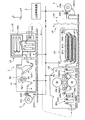
次に、第1実施形態の処理装置U3としての露光装置(基板処理装置)の構成について、図2から図4を参照して説明する。図2は、第1実施形態の露光装置(基板処理装置)の全体構成を示す図である。図3は、図2に示す露光装置の照明領域及び投影領域の配置を示す図である。図4は、図2に示す露光装置の照明光学系及び投影光学系の構成を示す図である。
<Exposure device (substrate processing device)>
Next, the configuration of an exposure apparatus (substrate processing apparatus) as the processing apparatus U3 of the first embodiment will be described with reference to FIGS. FIG. 2 is a view showing the overall configuration of the exposure apparatus (substrate processing apparatus) of the first embodiment. FIG. 3 is a view showing the arrangement of illumination areas and projection areas of the exposure apparatus shown in FIG. FIG. 4 is a diagram showing the configuration of the illumination optical system and the projection optical system of the exposure apparatus shown in FIG.
図2に示すように、処理装置U3は、露光装置(処理機構)EXと、搬送装置9とを含む。露光装置EXは、搬送装置9により基板P(シート、フィルム等)を供給されている。露光装置EXは、いわゆる走査露光装置であり、円筒マスクDMの回転と可撓性の基板Pの送り、すなわち図1中に示した回転ドラムDR5の回転とを同期駆動させつつ、円筒マスクDMに形成されているパターンの像を、投影倍率が等倍(×1)のマルチレンズ方式の投影光学系PL(PL1〜PL6)を介して基板Pに投影する。なお、図2に示す露光装置EXは、XYZ直交座標系のY軸を、円筒マスクDMを構成する第1ドラム部材21の回転中心線AX1と平行に設定している。同様に、露光装置EXは、XYZ直交座標系のY軸を、回転ドラムDR5(以下、第2ドラム部材22とも呼ぶ)の回転中心線AX2と平行に設定している。
As shown in FIG. 2, the processing device U <b> 3 includes an exposure device (processing mechanism) EX and a transport device 9. The exposure apparatus EX is supplied with a substrate P (sheet, film, etc.) by the transport device 9. The exposure apparatus EX is a so-called scanning exposure apparatus. The cylindrical mask DM is rotated while the rotation of the cylindrical mask DM and the feeding of the flexible substrate P, that is, the rotation of the rotary drum DR5 shown in FIG. An image of the formed pattern is projected onto the substrate P via a multi-lens projection optical system PL (PL1 to PL6) having a projection magnification of equal magnification (× 1). In the exposure apparatus EX shown in FIG. 2, the Y axis of the XYZ orthogonal coordinate system is set parallel to the rotation center line AX1 of the
図2に示すように、露光装置EXは、マスク保持装置12、照明機構IU、投影光学系PL及び制御装置14を備える。露光装置EXは、マスク保持装置12に保持された円筒マスクDMを回転移動させるとともに、搬送装置9によって基板Pを搬送する。照明機構IUは、円筒マスクDMのパターン面(外周面)の一部(照明領域IR)を、照明光束EL1によって均一な明るさで円筒マスクDMの内側から照明する。投影光学系PLは、円筒マスクDM上の照明領域IRにおけるパターンの像を、搬送装置9と回転ドラムDR5によって搬送されている基板Pの一部(投影領域PA)に投影する。これにより、円筒マスクDMの外周面に沿って配置された所定のパターン(マスクパターン)の像が基板P上に走査露光される。制御装置14は、露光装置EXの各部や搬送装置9を連携制御し、各部や搬送装置9に所定の動作を実行させる。
As shown in FIG. 2, the exposure apparatus EX includes a
なお、制御装置14は、上述したデバイス製造システムの複数の処理装置U1〜Unを統括して制御する上位制御装置5の一部又は全部であってもよい。また、制御装置14は、上位制御装置5に制御され、上位制御装置5とは別の装置であってもよい。制御装置14は、例えば、コンピュータシステムを含む。コンピュータシステムは、例えば、CPU及び各種メモリーやOS、周辺機器等のハードウェアを含む。処理装置U3の各部の動作の過程は、プログラムの形式でコンピュータ読み取り可能な記録媒体の記憶部に記憶されており、このプログラムをコンピュータシステムが読み出して実行することによって、各種処理が行われる。コンピュータシステムは、インターネット或いはイントラネットシステムに接続可能な場合、ホームページ提供環境(あるいは表示環境)も含む。また、コンピュータ読み取り可能な記録媒体は、フレキシブルディスク、光磁気ディスク、ROM、CD−ROM等の可搬媒体、コンピュータシステムに内蔵されるハードディスク等の記憶装置を含む。コンピュータ読み取り可能な記録媒体は、インターネット等のネットワークや電話回線等の通信回線を介してプログラムを送信する場合の通信線のように、短時間の間、動的にプログラムを保持するもの、その場合のサーバやクライアントとなるコンピュータシステム内部の揮発性メモリーのように、一定時間プログラムを保持しているものも含む。また、プログラムは、処理装置U3の機能の一部を実現するためのものでもよく、処理装置U3の機能をコンピュータシステムにすでに記録されているプログラムとの組み合わせで実現できるものでもよい。上位制御装置5は、制御装置14と同様に、コンピュータシステムを利用して実現することができる。
The
図2に示すように、マスク保持装置12は、円筒マスクDMを保持する第1ドラム部材21、第1ドラム部材21を支持するガイドローラ23、制御装置14の制御指令により第1駆動部26が第1ドラム部材21を駆動する駆動ローラ24及び第1ドラム部材21の位置を検出する第1検出器25を備える。
As shown in FIG. 2, the
第1ドラム部材21は、所定の軸となる回転中心線AX1(以下、第1中心軸AX1とも呼ぶ)から一定半径で湾曲した曲面を有する円筒部材であって、所定の軸の周りを回転する。第1ドラム部材21は、円筒マスクDM上の照明領域IRが配置される第1面P1を形成する。本実施形態において、第1面P1は、線分(母線)をこの線分に平行な軸(第1中心軸AX1)周りに回転した面(以下、円筒面という)を含む。円筒面は、例えば、円筒の外周面、円柱の外周面等である。第1ドラム部材21は、例えばガラスや石英等で構成され、一定の肉厚を有する円筒状であり、その外周面(円筒面)が第1面P1を形成する。すなわち、本実施形態において、円筒マスクDM上の照明領域IRは、回転中心線AX1から一定の半径r1を持つ円筒面状に湾曲している。このように、第1ドラム部材21は、所定の軸である回転中心線AX1から一定半径で湾曲した曲面を有している。そして、第1ドラム部材21は、駆動ローラ24に駆動されて、所定の軸である回転中心線AX1の周りを回転することができる。
The
円筒マスクDMは、例えば平坦性の良い短冊状の極薄ガラス板(例えば厚さ100μm〜500μm)の一方の面にクロム等の遮光層でパターンを形成した透過型の平面状シートマスクとして作成される。マスク保持装置12は、円筒マスクDMを第1ドラム部材21の外周面の曲面に倣って湾曲させ、この曲面に巻き付けた(貼り付けた)状態で使用される。円筒マスクDMは、パターンが形成されていないパターン非形成領域を有し、パターン非形成領域において第1ドラム部材21に取付けられている。円筒マスクDMは、第1ドラム部材21に対してリリース可能である。
The cylindrical mask DM is prepared as a transmission type planar sheet mask in which a pattern is formed with a light-shielding layer of chromium or the like on one surface of a strip-shaped ultrathin glass plate having a good flatness (for example, a thickness of 100 μm to 500 μm). The The
なお、円筒マスクDMを極薄ガラス板で構成し、その円筒マスクDMを透明円筒母材による第1ドラム部材21に巻き付ける代わりに、透明円筒母材による第1ドラム部材21の外周面に直接クロム等の遮光層によるマスクパターンを描画形成して一体化してもよい。この場合も、第1ドラム部材21が円筒マスクDMのパターンの支持部材として機能する。
The cylindrical mask DM is made of an ultrathin glass plate, and instead of winding the cylindrical mask DM around the
第1検出器25は、第1ドラム部材21の回転位置を光学的に検出するもので、例えばロータリーエンコーダ等で構成される。第1検出器25は、検出した第1ドラム部材21の回転位置を示す情報、例えば、後述するエンコーダヘッドからの2相信号等を制御装置14に出力する。電動モーター等のアクチュエータを含む第1駆動部26は、制御装置14から入力される制御信号に従って、駆動ローラ24を回転させるためのトルク及び回転速度を調整する。制御装置14は、第1検出器25による検出結果に基づいて第1駆動部26を制御することによって、第1ドラム部材21の回転位置を制御する。そして、制御装置14は、第1ドラム部材21に保持されている円筒マスクDMの回転位置と回転速度の一方又は双方を制御する。
The
第2ドラム部材22は、所定の軸となる回転中心線AX2(以下、第2中心軸AX2とも呼ぶ)から一定半径で湾曲した曲面(第1曲面)を有する円筒部材であって、所定の軸の周りを回転する回転ドラムである。第2ドラム部材22は、投影光学系PLからの結像光束が投射される基板P上の投影領域PAを含む一部分を円弧状(円筒状)に支持する第2面(支持面)P2を形成する。また、第2ドラム部材22は、電動モーター等のアクチュエータを含む第2駆動部36から供給されるトルクによって回転する駆動ローラDR5である。
The
このように、第2ドラム部材22は、駆動ローラDR5であるとともに、露光(処理)対象の基板Pを支持する基板支持部材(基板ステージ)を兼ねている。すなわち、第2ドラム部材22は、露光装置EXの一部であってもよい。そして、第2ドラム部材22は、第2ドラム部材22の回転中心線AX2(第2中心軸AX2)の周りに回転可能であり、基板Pは、第2ドラム部材22上の外周面(円筒面)に倣って円筒面状に湾曲し、湾曲した部分の一部に投影領域PAが配置される。
As described above, the
本実施形態では、投影領域PAに達する結像光束EL2のうち、投影領域PAの各中心点を通る主光線は、図2に示すように、第2ドラム部材22の第2中心軸AX2からみて、中心面P3を挟んで周方向で角度θの位置にそれぞれ配置され第1特定位置PX1、第2特定位置PX2に到達する。そして、回転中心線AX2からみて、第1特定位置PX1と、第2特定位置PX2との間にある、特定位置PXは、第2ドラム部材22の曲面にある基板Pの平均的に露光された領域の中心となっている。
In the present embodiment, out of the imaging light beam EL2 reaching the projection area PA, the principal ray passing through each center point of the projection area PA is viewed from the second central axis AX2 of the
搬送装置9は、駆動ローラDR4、第2ドラム部材22(駆動ローラDR5)、駆動ローラDR6を備えている。搬送装置9は、基板Pが、第1特定位置PX1、特定位置PX及び第2特定位置PX2を通過するように基板Pを搬送する搬送方向に、基板Pを移動させる。第2駆動部36は、制御装置14から出力される制御信号に従って、第2ドラム部材22を回転させるトルクを調整する。
The transport device 9 includes a drive roller DR4, a second drum member 22 (drive roller DR5), and a drive roller DR6. The transport device 9 moves the substrate P in the transport direction in which the substrate P is transported so that the substrate P passes through the first specific position PX1, the specific position PX, and the second specific position PX2. The
本実施形態において、搬送経路の上流から駆動ローラDR4へ搬送されてきた基板Pは、駆動ローラDR4を経由して第1ガイド部材33に案内され、第2ドラム部材22へ搬送される。基板Pは、第2ドラム部材22の表面に支持され、第2ガイド部材33へ搬送される。第2ガイド部材33を経由した基板Pは、搬送経路の下流へ搬送される。なお、第2ドラム部材22(駆動ローラDR5)の回転中心線AX2と、駆動ローラDR4、DR6の各回転中心線とは、何れもY軸と平行になるように設定される。
In the present embodiment, the substrate P that has been transported from the upstream of the transport path to the drive roller DR4 is guided to the
第2ドラム部材22の周囲には、基板Pが搬送される搬送方向を規制し、かつ基板Pを案内する第1ガイド部材32及び第2ガイド部材32が配置されている。第2ドラム部材22は、基板Pの一部分が巻き付けられて、基板Pが第2面P2の曲面に接し始める搬送方向の進入位置IAから基板Pが第2面P2の曲面から離れ始める搬送方向の離脱位置OAまでの基板Pを支持する。第1ガイド部材32及び第2ガイド部材32は、例えば、基板Pの搬送方向に移動することによって、搬送経路において基板Pに働くテンション等を調整する。また、第1ガイド部材32及び第2ガイド部材33は、例えば、基板Pの搬送方向に移動することによって、第2ドラム部材22の外周に巻き付く、上述した進入位置IA及び離脱位置OA等を調整することができる。なお、搬送装置9、第1ガイド部材32及び第2ガイド部材33は、投影光学系PLの投影領域PAに沿って基板Pを搬送可能であればよく、搬送装置9、第1ガイド部材32及び第2ガイド部材33の構成は適宜変更可能である。
Around the
第2検出器35は、例えばロータリーエンコーダ等で構成され、第2ドラム部材22の回転位置を光学的に検出する。第2検出器35は、検出した第2ドラム部材22の回転位置を示す情報(例えば、後述するエンコーダヘッドEN1、EN2、EN3、EN4、EN5からの2相信号等)を制御装置14に出力する。制御装置14は、第2検出器35による検出結果に基づいて第2駆動部36を制御することによって、第2ドラム部材22の回転位置を制御し、第1ドラム部材21(円筒マスクDM)と第2ドラム部材22とを同期移動(同期回転)させる。なお、第2検出器35の詳細な構成については後述する。
The
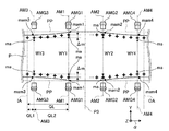
本実施形態の露光装置EXは、所謂、マルチレンズ方式の投影光学系PLを搭載することを想定した露光装置である。投影光学系PLは、円筒マスクDMのパターンにおける一部の像を投影する複数の投影モジュールを備える。例えば、図2では、中心面P3の左側に3つの投影モジュール(投影光学系)PL1、PL3、PL5がY方向に一定間隔で配置され、中心面P3の右側にも3つの投影モジュール(投影光学系)PL2、PL4、PL6がY方向に一定間隔で配置される。 The exposure apparatus EX of the present embodiment is an exposure apparatus that is assumed to be equipped with a so-called multi-lens projection optical system PL. The projection optical system PL includes a plurality of projection modules that project some images in the pattern of the cylindrical mask DM. For example, in FIG. 2, three projection modules (projection optical systems) PL1, PL3, PL5 are arranged at regular intervals in the Y direction on the left side of the central plane P3, and three projection modules (projection optics) are also arranged on the right side of the central plane P3. System) PL2, PL4, and PL6 are arranged at regular intervals in the Y direction.
このようなマルチレンズ方式の露光装置EXでは、複数の投影モジュールPL1〜PL6によって露光された領域(投影領域PA1〜PA6)のY方向の端部を走査によって互いに重ね合わせることによって、所望のパターンの全体像を投影する。このような露光装置EXは、円筒マスクDM上のパターンのY方向サイズが大きくなり、必然的にY方向の幅が大きな基板Pを扱う必要性が生じた場合でも、投影モジュールPLと、投影モジュールPLに対応する照明機構IU側のモジュールとをY方向に増設するだけで良いので、容易にパネルサイズ(基板Pの幅)の大型化に対応できると言った利点がある。 In such a multi-lens type exposure apparatus EX, the end portions in the Y direction of the areas exposed by the plurality of projection modules PL1 to PL6 (projection areas PA1 to PA6) are overlapped with each other by scanning, thereby forming a desired pattern. Project the whole picture. In such an exposure apparatus EX, even when the Y-direction size of the pattern on the cylindrical mask DM becomes large, and it becomes inevitably necessary to handle the substrate P having a large width in the Y-direction, the projection module PL and the projection module Since it is only necessary to add the module on the illumination mechanism IU side corresponding to the PL in the Y direction, there is an advantage that the panel size (the width of the substrate P) can be easily increased.
なお、露光装置EXは、マルチレンズ方式でなくてもよい。例えば、基板Pの幅方向の寸法がある程度小さい場合等に、露光装置EXは、1つの投影モジュールによってパターンの全幅の像を基板Pに投影してもよい。また、複数の投影モジュールPL1〜PL6は、それぞれ、1個のデバイスに対応するパターンを投影してもよい。すなわち、露光装置EXは、複数個のデバイス用のパターンを、複数の投影モジュールによって並行して投影してもよい。 The exposure apparatus EX may not be a multi-lens system. For example, when the dimension in the width direction of the substrate P is small to some extent, the exposure apparatus EX may project an image of the full width of the pattern onto the substrate P by one projection module. Further, each of the plurality of projection modules PL1 to PL6 may project a pattern corresponding to one device. That is, the exposure apparatus EX may project a plurality of device patterns in parallel by a plurality of projection modules.
本実施形態の照明機構IUは、光源装置13及び照明光学系を備える。照明光学系は、複数の投影モジュールPL1〜PL6の各々に対応してY軸方向に並んだ複数(例えば6つ)の照明モジュールILを備える。光源装置13は、例えば水銀ランプ等のランプ光源、又はレーザーダイオード、発光ダイオード(LED)等の固体光源を含む。光源装置が射出する照明光は、例えばランプ光源から射出される輝線(g線、h線、i線)、KrFエキシマレーザ光(波長248nm)等の遠紫外光(DUV光)、ArFエキシマレーザ光(波長193nm)等である。光源装置から射出された照明光は、照度分布が均一化されて、例えば光ファイバー等の導光部材を介して、複数の照明モジュールILに振り分けられる。
The illumination mechanism IU of this embodiment includes a
複数の照明モジュールILのそれぞれは、レンズ等の複数の光学部材を含む。本実施形態において、光源装置から出射して複数の照明モジュールILのいずれかを通る光を照明光束EL1と称する。複数の照明モジュールILのそれぞれは、例えばインテグレータ光学系、ロッドレンズ、フライアイレンズ等を含み、均一な照度分布の照明光束EL1によって照明領域IRを照明する。本実施形態において、複数の照明モジュールILは、円筒マスクDMの内側に配置されている。複数の照明モジュールILのそれぞれは、円筒マスクDMの内側から円筒マスクDMの外周面に形成されたマスクパターンの各照明領域IRを照明する。 Each of the plurality of illumination modules IL includes a plurality of optical members such as lenses. In the present embodiment, light emitted from the light source device and passing through any one of the plurality of illumination modules IL is referred to as illumination light beam EL1. Each of the plurality of illumination modules IL includes, for example, an integrator optical system, a rod lens, a fly-eye lens, and the like, and illuminates the illumination region IR with an illumination light beam EL1 having a uniform illuminance distribution. In the present embodiment, the plurality of illumination modules IL are arranged inside the cylindrical mask DM. Each of the plurality of illumination modules IL illuminates each illumination region IR of the mask pattern formed on the outer peripheral surface of the cylindrical mask DM from the inside of the cylindrical mask DM.
図3は、本実施形態における照明領域IR及び投影領域PAの配置を示す図である。なお、図3には、第1ドラム部材21に配置された円筒マスクDM上の照明領域IRを−Z側から見た平面図(図3中の左側の図)と、第2ドラム部材22に配置された基板P上の投影領域PAを+Z側から見た平面図(図3中の右側の図)とが図示されている。図3中の符号Xsは、第1ドラム部材21又は第2ドラム部材22の回転方向(移動方向)を示す。
FIG. 3 is a diagram showing the arrangement of the illumination area IR and the projection area PA in the present embodiment. 3 is a plan view (on the left side in FIG. 3) of the illumination area IR on the cylindrical mask DM disposed on the
複数の照明モジュールILは、それぞれ、円筒マスクDM上の第1から第6照明領域IR1〜IR6を照明する。例えば、第1照明モジュールILは、第1照明領域IR1を照明し、第2照明モジュールILは第2照明領域IR2を照明する。 Each of the plurality of illumination modules IL illuminates the first to sixth illumination regions IR1 to IR6 on the cylindrical mask DM. For example, the first illumination module IL illuminates the first illumination region IR1, and the second illumination module IL illuminates the second illumination region IR2.
第1照明領域IR1は、Y方向に細長い台形状の領域として説明するが、投影光学系(投影モジュール)PLのように、中間像面を形成する構成の投影光学系の場合は、その中間像の位置に台形開口を有する視野絞り板を配置できるため、その台形開口を包含する長方形の領域としても良い。第3照明領域IR3及び第5照明領域IR5は、それぞれ、第1照明領域IR1と同様の形状の領域であり、Y軸方向に一定間隔を空けて配置されている。また、第2照明領域IR2は、中心面P3に関して第1照明領域IR1と対称的な台形状(又は長方形)の領域である。第4照明領域IR4及び第6照明領域IR6は、それぞれ、第2照明領域IR2と同様の形状の領域であり、Y軸方向に一定間隔を空けて配置されている。 The first illumination region IR1 will be described as a trapezoidal region elongated in the Y direction. However, in the case of a projection optical system configured to form an intermediate image plane, such as the projection optical system (projection module) PL, the intermediate image Since a field stop plate having a trapezoidal opening can be arranged at the position of, a rectangular region including the trapezoidal opening may be used. The third illumination region IR3 and the fifth illumination region IR5 are regions having the same shape as the first illumination region IR1, respectively, and are arranged at regular intervals in the Y-axis direction. The second illumination region IR2 is a trapezoidal (or rectangular) region symmetrical to the first illumination region IR1 with respect to the center plane P3. The fourth illumination region IR4 and the sixth illumination region IR6 are regions having the same shape as the second illumination region IR2, respectively, and are arranged at regular intervals in the Y-axis direction.
図3に示すように、第1から第6照明領域IR1〜IR6のそれぞれは、第1面P1の周方向に沿って見た場合に、隣り合う台形状の照明領域の斜辺部の三角部が重なるように(オーバーラップするように)配置されている。そのため、例えば、第1ドラム部材21の回転によって第1照明領域IR1を通過する円筒マスクDM上の第1領域A1は、第1ドラム部材21の回転によって第2照明領域IR2を通過する円筒マスクDM上の第2領域A2と一部重複する。
As shown in FIG. 3, each of the first to sixth illumination regions IR1 to IR6 has a triangular portion of a hypotenuse portion of an adjacent trapezoidal illumination region when viewed along the circumferential direction of the first surface P1. They are arranged so that they overlap (overlapping). Therefore, for example, the first region A1 on the cylindrical mask DM that passes through the first illumination region IR1 by the rotation of the
本実施形態において、円筒マスクDMは、パターンが形成されているパターン形成領域A3と、パターンが形成されていないパターン非形成領域A4とを含む。そのパターン非形成領域A4は、パターン形成領域A3を枠状に囲むように配置されており、照明光束EL1を遮光する特性を有する。円筒マスクDMのパターン形成領域A3は、第1ドラム部材21の回転に伴って移動方向Xsに移動し、パターン形成領域A3のうちのY軸方向の各部分領域は、第1から第6照明領域IR1〜IR6のいずれかを通過する。換言すると、第1から第6照明領域IR1〜IR6は、パターン形成領域A3のY軸方向の全幅をカバーするように、配置されている。
In the present embodiment, the cylindrical mask DM includes a pattern formation region A3 where a pattern is formed and a pattern non-formation region A4 where a pattern is not formed. The pattern non-formation region A4 is arranged so as to surround the pattern formation region A3 in a frame shape, and has a characteristic of shielding the illumination light beam EL1. The pattern formation area A3 of the cylindrical mask DM moves in the movement direction Xs with the rotation of the
図2に示すように、Y軸方向に並ぶ複数の投影モジュールPL1〜PL6のそれぞれは、第1から第6照明モジュールILのそれぞれと1対1で対応しており、対応する照明モジュールによって照明される照明領域IR内に現れる円筒マスクDMの部分的なパターンの像を、基板P上の各投影領域PAに投影する。 As shown in FIG. 2, each of the plurality of projection modules PL1 to PL6 arranged in the Y-axis direction has a one-to-one correspondence with each of the first to sixth illumination modules IL, and is illuminated by the corresponding illumination module. An image of a partial pattern of the cylindrical mask DM that appears in the illumination area IR is projected onto each projection area PA on the substrate P.
例えば、第1投影モジュールPL1は、第1照明モジュールILに対応し、第1照明モジュールILによって照明される第1照明領域IR1(図3参照)における円筒マスクDMのパターンの像を、基板P上の第1投影領域PA1に投影する。第3投影モジュールPL3、第5投影モジュールPL5は、それぞれ、第3、第5照明モジュールILと対応している。第3投影モジュールPL3及び第5投影モジュールPL5は、Y軸方向から見ると、第1投影モジュールPL1と重なる位置に配置されている。 For example, the first projection module PL1 corresponds to the first illumination module IL, and displays an image of the pattern of the cylindrical mask DM in the first illumination region IR1 (see FIG. 3) illuminated by the first illumination module IL on the substrate P. Is projected onto the first projection area PA1. The third projection module PL3 and the fifth projection module PL5 correspond to the third and fifth illumination modules IL, respectively. The third projection module PL3 and the fifth projection module PL5 are arranged at a position overlapping the first projection module PL1 when viewed from the Y-axis direction.
また、第2投影モジュールPL2は、第2照明モジュールILに対応し、第2照明モジュールILによって照明される第2照明領域IR2(図3参照)における円筒マスクDMのパターンの像を、基板P上の第2投影領域PA2に投影する。第2投影モジュールPL2は、Y軸方向から見ると、第1投影モジュールPL1に対して中心面P3を挟んで対称的な位置に配置されている。 The second projection module PL2 corresponds to the second illumination module IL, and displays an image of the pattern of the cylindrical mask DM in the second illumination region IR2 (see FIG. 3) illuminated by the second illumination module IL on the substrate P. Is projected onto the second projection area PA2. When viewed from the Y-axis direction, the second projection module PL2 is disposed at a symmetrical position with respect to the first projection module PL1 across the center plane P3.
第4投影モジュールPL4、第6投影モジュールPL6は、それぞれ、第4、第6照明モジュールILと対応して配置され、第4投影モジュールPL4及び第6投影モジュールPL6は、Y軸方向から見て、第2投影モジュールPL2と重なる位置に配置されている。 The fourth projection module PL4 and the sixth projection module PL6 are respectively arranged corresponding to the fourth and sixth illumination modules IL, and the fourth projection module PL4 and the sixth projection module PL6 are viewed from the Y-axis direction, It is arranged at a position overlapping the second projection module PL2.
なお、本実施形態において、照明機構IUの各照明モジュールILから円筒マスクDM上の各照明領域IR1〜IR6に達する光を照明光束EL1とする。また、各照明領域IR1〜IR6中に現れる円筒マスクDMの部分パターンに応じた強度分布変調を受けて各投影モジュールPL1〜PL6に入射して各投影領域PA1〜PA6に達する光を、結像光束EL2とする。そして、各投影領域PA1〜PA6に達する結像光束EL2のうち、投影領域PA1〜PA6の各中心点を通る主光線は、図2に示すように、第2ドラム部材22の第2中心軸AX2からみて、中心面P3を挟んで周方向で角度θの位置(特定位置)にそれぞれ配置される。
In the present embodiment, light reaching each illumination region IR1 to IR6 on the cylindrical mask DM from each illumination module IL of the illumination mechanism IU is defined as an illumination light beam EL1. Further, the light reaching the projection areas PA1 to PA6 after receiving the intensity distribution modulation corresponding to the partial pattern of the cylindrical mask DM appearing in the illumination areas IR1 to IR6 and entering the projection modules PL1 to PL6 Let it be EL2. Of the imaging light beam EL2 reaching the projection areas PA1 to PA6, the principal ray passing through the center points of the projection areas PA1 to PA6 is, as shown in FIG. 2, the second central axis AX2 of the
図3に示すように、第1照明領域IR1におけるパターンの像は第1投影領域PA1に投影され、第3照明領域IR3におけるパターンの像は、第3投影領域PA3に投影され、第5照明領域IR5におけるパターンの像は、第5投影領域PA5に投影される。本実施形態において、第1投影領域PA1、第3投影領域PA3及び第5投影領域PA5は、Y軸方向に一列に並ぶように配置される。 As shown in FIG. 3, the pattern image in the first illumination area IR1 is projected onto the first projection area PA1, the pattern image in the third illumination area IR3 is projected onto the third projection area PA3, and the fifth illumination area The pattern image in IR5 is projected onto the fifth projection area PA5. In the present embodiment, the first projection area PA1, the third projection area PA3, and the fifth projection area PA5 are arranged in a line in the Y-axis direction.
また、第2照明領域IR2におけるパターンの像は、第2投影領域PA2に投影される。本実施形態において、第2投影領域PA2は、Y軸方向から見て、中心面P3に関して第1投影領域PA1と対称的に配置される。また、第4照明領域IR4におけるパターンの像は、第4投影領域PA4に投影され、第6照明領域IR6におけるパターンの像は、第6投影領域PA6に投影される。本実施形態において、第2投影領域PA2、第4投影領域PA4及び第6投影領域PA6は、Y軸方向に一列に並ぶように配置される。 The pattern image in the second illumination area IR2 is projected onto the second projection area PA2. In the present embodiment, the second projection area PA2 is arranged symmetrically with the first projection area PA1 with respect to the center plane P3 when viewed from the Y-axis direction. The pattern image in the fourth illumination area IR4 is projected on the fourth projection area PA4, and the pattern image in the sixth illumination area IR6 is projected on the sixth projection area PA6. In the present embodiment, the second projection area PA2, the fourth projection area PA4, and the sixth projection area PA6 are arranged in a line in the Y-axis direction.
第1から第6投影領域PA1〜PA6のそれぞれは、第2面P2の周方向に沿って見た場合に、第2中心軸AX2に平行な方向において隣り合う投影領域(奇数番目と偶数番目)同士の端部(台形の三角部分)が重なるように配置されている。そのため、例えば、第2ドラム部材22の回転によって第1投影領域PA1を通過する基板P上の第3領域A5は、第2ドラム部材22の回転によって第2投影領域PA2を通過する基板P上の第4領域A6と一部重複する。第1投影領域PA1と第2投影領域PA2は、第3領域A5と第4領域A6が重複する領域での露光量が、重複しない領域の露光量と実質的に同じになるように、それぞれの形状等が設定されている。そして、第1〜第6投影領域PA1〜PA6は、基板P上に露光される露光領域A7のY方向の全幅をカバーするように、配置されている。
Each of the first to sixth projection areas PA1 to PA6 is adjacent to each other in the direction parallel to the second central axis AX2 (odd number and even number) when viewed along the circumferential direction of the second surface P2. It arrange | positions so that the edge part (trapezoid triangular part) of each other may overlap. Therefore, for example, the third area A5 on the substrate P passing through the first projection area PA1 due to the rotation of the
次に、本実施形態の投影光学系PLの詳細構成について図4を参照して説明する。なお、本実施形態において、第2投影モジュールPL2〜第5投影モジュールPL5のそれぞれは、第1投影モジュールPL1と同様の構成である。このため、投影光学系PLを代表して、第1投影モジュールPL1の構成について説明し、第2投影モジュールPL2〜第5投影モジュールPL5のそれぞれの説明は省略する。 Next, a detailed configuration of the projection optical system PL of the present embodiment will be described with reference to FIG. In the present embodiment, each of the second projection module PL2 to the fifth projection module PL5 has the same configuration as the first projection module PL1. Therefore, the configuration of the first projection module PL1 will be described on behalf of the projection optical system PL, and the description of each of the second projection module PL2 to the fifth projection module PL5 will be omitted.
図4に示す第1投影モジュールPL1は、第1照明領域IR1に配置された円筒マスクDMのパターンの像を中間像面P7に結像する第1光学系41と、第1光学系41が形成した中間像の少なくとも一部を基板Pの第1投影領域PA1に再結像する第2光学系42と、中間像が形成される中間像面P7に配置された第1視野絞り43とを備える。
The first projection module PL1 shown in FIG. 4 includes a first
また、第1投影モジュールPL1は、フォーカス補正光学部材44、像シフト補正光学部材45、ローテーション補正機構46及び倍率補正用光学部材47を備えている。フォーカス補正光学部材44は、基板P上に形成されるマスクのパターン像(以下、投影像という)のフォーカス状態を微調整するフォーカス調整装置である。また、像シフト補正光学部材45は、投影像を像面内で微少に横シフトさせるシフト調整装置である。倍率補正用光学部材47は、投影像の倍率を微少補正する倍率調整装置である。ローテーション補正機構46は、投影像を像面内で微少回転させるシフト調整装置である。
Further, the first projection module PL1 includes a focus correction
円筒マスクDMのパターンからの結像光束EL2は、第1照明領域IR1から法線方向(D1)に出射し、フォーカス補正光学部材44を通って像シフト補正光学部材45に入射する。像シフト補正光学部材45を透過した結像光束EL2は、第1光学系41の要素である第1偏向部材50の第1反射面(平面鏡)p4で反射され、第1レンズ群51を通って第1凹面鏡52(反射面p6)で反射され、再び第1レンズ群51を通って第1偏向部材50の第2反射面(平面鏡)p5で反射されて、第1視野絞り43に入射する。第1視野絞り43を通った結像光束EL2は、第2光学系42の要素である第2偏向部材57の第3反射面(平面鏡)p8で反射され、第2レンズ群58を通って第2凹面鏡59で反射され、再び第2レンズ群58を通って第2偏向部材57の第4反射面(平面鏡)p9で反射されて、倍率補正用光学部材47に入射する。倍率補正用光学部材47から出射した結像光束EL2は、基板P上の第1投影領域PA1に入射し、第1照明領域IR1内に現れるパターンの像が第1投影領域PA1に等倍(×1)で投影される。
The imaging light beam EL2 from the pattern of the cylindrical mask DM exits from the first illumination region IR1 in the normal direction (D1), and enters the image shift correction
図2に示す円筒マスクDMの半径を半径r1とし、第2ドラム部材22に巻き付いた基板Pの円筒状の表面の半径を半径r2として、半径r1と半径r2とを等しくした場合、各投影モジュールPL1〜PL6のマスク側における結像光束EL2の主光線は、円筒マスクDMの中心軸線AX1を通るように傾けられるが、その傾き角は、基板P側における結像光束EL2の主光線の傾き角θ(中心面P3に対して±θ)と同じになる。
When the radius of the cylindrical mask DM shown in FIG. 2 is the radius r1, the radius of the cylindrical surface of the substrate P wound around the
第2偏向部材57の第3反射面p8が第2光軸AX4となす角度θ3は、第1偏向部材50の第2反射面p5が第1光軸AX3となす角度θ2と実質的に同じである。また、第2偏向部材57の第4反射面p9が第2光軸AX4となす角度θ4は、第1偏向部材50の第1反射面p4が第1光軸AX3となす角度θ1と実質的に同じである。上述した傾き角θを与えるため、図4に示した第1偏向部材50の第1反射面p4の第1光軸AX3に対する角度θ1を45°よりもΔθ1だけ小さくし、第2偏向部材57の第4反射面p9の第2光軸AX4に対する角度θ4を45°よりもΔθ4だけ小さくする。Δθ1とΔθ4は、図2中に示した角度θに対して、Δθ1=Δθ4=θ/2の関係に設定される。
The angle θ3 formed by the third reflecting surface p8 of the second deflecting
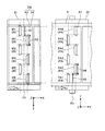
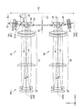
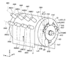
図5は、図2の処理装置(露光装置)に適用される回転ドラムの斜視図である。図6は、図2の処理装置(露光装置)に適用される検出プローブと読み取り装置との関係を説明するための斜視図である。図7は、第1実施形態に係るスケール円盤SDを回転中心線AX2方向にみた、読み取り装置の位置を説明するための説明図である。なお、図5においては、便宜上、第2から第4投影領域PA2〜PA4のみを図示し、第1、第5、第6投影領域PA1、PA5、PA6の図示を省略している。 FIG. 5 is a perspective view of a rotating drum applied to the processing apparatus (exposure apparatus) of FIG. FIG. 6 is a perspective view for explaining the relationship between a detection probe and a reading device applied to the processing apparatus (exposure apparatus) in FIG. FIG. 7 is an explanatory diagram for explaining the position of the reading device when the scale disk SD according to the first embodiment is viewed in the direction of the rotation center line AX2. In FIG. 5, for convenience, only the second to fourth projection areas PA2 to PA4 are shown, and the first, fifth, and sixth projection areas PA1, PA5, and PA6 are not shown.
図2に示す第2検出器35は、第2ドラム部材22の回転位置を光学的に検出するものであって、高真円度のスケール円盤(スケール部材)SDと、読み取り装置であるエンコーダヘッドEN1、EN2、EN3、EN4、EN5を含む。
The
スケール円盤SDは、第2ドラム部材22の回転軸STと直交する第2ドラム部材22の端部に固定されている。このため、スケール円盤SDは、回転中心線AX2回りに回転軸STと共に一体的に回転する。スケール円盤SDの外周面には、スケール部GPとして例えば目盛(格子)が刻設されている。スケール部GPは、第2ドラム部材22が回転する周方向に沿って環状に配列され、かつ第2ドラム部材22とともに回転軸ST(第2中心軸AX2)の周囲を回転する。エンコーダヘッドEN1、EN2、EN3、EN4、EN5は、回転軸ST(第2中心軸AX2)からみてスケール部GPの周囲に配置されている。エンコーダヘッドEN1、EN2、EN3、EN4、EN5は、スケール部GPと対向配置され、スケール部GPを非接触で読み取ることができる。また、エンコーダヘッドEN1、EN2、EN3、EN4、EN5は、第2ドラム部材22の周方向の異なる位置に配置されている。
The scale disk SD is fixed to the end of the
エンコーダヘッドEN1、EN2、EN3、EN4、EN5は、スケール部GPの接線方向(XZ面内)の変位の変動に対して計測感度(検出感度)を有する読み取り装置である。図5に示すように、エンコーダヘッドEN1、EN2、EN3、EN4、EN5の設置方位(回転中心線AX2を中心としたXZ面内での角度方向)を設置方位線Le1、Le2、Le3、Le4、Le5で表す場合、図7に示すように、設置方位線Le1、Le2が、中心面P3に対して角度±θ°になるように、エンコーダヘッドEN1、EN2が配置される。なお、本実施形態では、例えば角度θは15°である。 The encoder heads EN1, EN2, EN3, EN4, and EN5 are reading devices having measurement sensitivity (detection sensitivity) with respect to variation in displacement in the tangential direction (in the XZ plane) of the scale part GP. As shown in FIG. 5, the installation directions (angle directions in the XZ plane with the rotation center line AX2 as the center) of the encoder heads EN1, EN2, EN3, EN4, EN5 are set as the installation direction lines Le1, Le2, Le3, Le4, When represented by Le5, as shown in FIG. 7, the encoder heads EN1 and EN2 are arranged such that the installation orientation lines Le1 and Le2 are at an angle ± θ ° with respect to the center plane P3. In the present embodiment, for example, the angle θ is 15 °.
図4に示す投影モジュールPL1〜PL6は、基板Pを被処理物体とし、基板Pに光を照射する照射処理を施す露光装置EXの処理部である。露光装置EXは、基板Pに対して2つの結像光束EL2の主光線が基板Pに入射する。投影モジュールPL1、PL3、PL5が第1処理部となり、投影モジュールPL2、PL4、PL6が第2処理部となり、基板Pに対して2つの結像光束EL2の主光線が基板Pに入射するそれぞれの位置が基板Pに光を照射する照射処理を施す特定位置となる。特定位置は、第2ドラム部材22の第2中心軸AX2からみて、第2ドラム部材22上の曲面の基板Pにおける、中心面P3を挟んで周方向で角度±θの位置である。エンコーダヘッドEN1の設置方位線Le1は、奇数番目の投影モジュールPL1、PL3、PL5の各投影領域(投影視野)PA1、PA3、PA5の中心点を通る主光線の中心面P3に対する傾き角θと一致し、ヘッドEN2の設置方位線Le2は、偶数番目の投影モジュールPL2、PL4、PL6の各投影領域(投影視野)PA2、PA4、PA6の中心点を通る主光線の中心面P3に対する傾き角θと一致している。このため、エンコーダヘッドEN1は、第1特定位置PX1と第2中心軸AX2とを結ぶ方向に位置するスケール部GPを読み取る読み取り装置となる。そして、エンコーダヘッドEN2は、第2特定位置PX2と第2中心軸AX2とを結ぶ方向に位置するスケール部GPを読み取る読み取り装置となる。
Projection modules PL <b> 1 to PL <b> 6 shown in FIG. 4 are processing units of the exposure apparatus EX that performs irradiation processing for irradiating the substrate P with light, using the substrate P as an object to be processed. In the exposure apparatus EX, the principal rays of the two imaging light beams EL2 enter the substrate P with respect to the substrate P. The projection modules PL1, PL3, and PL5 serve as the first processing unit, and the projection modules PL2, PL4, and PL6 serve as the second processing unit, and the principal rays of the two imaging light beams EL2 are incident on the substrate P with respect to the substrate P. The position is a specific position where the irradiation process for irradiating the substrate P with light is performed. The specific position is a position at an angle ± θ in the circumferential direction with respect to the center plane P3 on the curved substrate P on the
エンコーダヘッドEN4は、基板Pの搬送方向の後方側、つまり露光位置(投影領域)の手前に配置されており、基板Pの搬送方向の後方側に向かってエンコーダヘッドEN1の設置方位線Le1を回転中心線AX2の軸回りに回転した設置方位線Le4上に設定される。また、エンコーダヘッドEN5は、基板Pの搬送方向の後方側に向かってエンコーダヘッドEN1の設置方位線Le1を回転中心線AX2の軸回りに回転した設置方位線Le5上に設定される。 The encoder head EN4 is arranged on the rear side in the transport direction of the substrate P, that is, before the exposure position (projection area), and rotates the installation direction line Le1 of the encoder head EN1 toward the rear side in the transport direction of the substrate P. It is set on the installation direction line Le4 rotated around the axis of the center line AX2. Further, the encoder head EN5 is set on the installation direction line Le5 obtained by rotating the installation direction line Le1 of the encoder head EN1 around the axis of the rotation center line AX2 toward the rear side in the transport direction of the substrate P.
また、エンコーダヘッドEN3は、エンコーダヘッドEN1、EN2に対して、回転中心線AX2を挟んだ反対側に配置され、その設置方位線Le3は中心面P3上に設定されている。 The encoder head EN3 is arranged on the opposite side of the encoder heads EN1 and EN2 with the rotation center line AX2 interposed therebetween, and the installation orientation line Le3 is set on the center plane P3.
スケール部材であるスケール円盤SDは、低熱膨張の金属、ガラス、セラミックス等を母材とし、計測分解能を高めるために、なるべく大きな直径(例えば直径20cm以上)になるように作られる。図5では、第2ドラム部材22の直径に対してスケール円盤SDの直径は小さく図示されているが、第2ドラム部材22の外周面のうち、基板Pが巻き付けられる外周面の直径と、スケール円盤SDのスケール部GPの直径とを揃える(ほぼ一致させる)ことで、所謂、計測アッベ誤差をさらに小さくすることができる。
The scale disk SD, which is a scale member, is made so as to have a diameter as large as possible (for example, a diameter of 20 cm or more) in order to increase measurement resolution, using a low thermal expansion metal, glass, ceramics or the like as a base material. In FIG. 5, the diameter of the scale disk SD is smaller than the diameter of the
スケール部GPの周方向に刻設される目盛(格子)の最小ピッチは、スケール円盤SDを加工する目盛刻線装置等の性能によって制限されている。このため、スケール円盤SDの直径を大きくすれば、それに応じて最小ピッチに対応した角度計測分解能も高めることが出来る。 The minimum pitch of the scale (lattice) engraved in the circumferential direction of the scale part GP is limited by the performance of a scale engraving device that processes the scale disk SD. For this reason, if the diameter of the scale disk SD is increased, the angle measurement resolution corresponding to the minimum pitch can be increased accordingly.
スケール部GPを読み取るエンコーダヘッドEN1、EN2が配置される設置方位線Le1、Le2の方向を、回転中心線AX2からみたときに、基板Pに対して結像光束EL2の主光線が基板Pに入射する方向と同一にすることにより、例えば、回転軸STを支持する軸受(ベアリング)の僅かなガタ(2μm〜3μm程度)によって第2ドラム部材22がX方向にシフトした場合でも、このシフトによって投影領域PA1〜PA6内で発生し得る基板Pの搬送方向(Xs)に関する位置誤差を、エンコーダヘッドEN1、EN2によって高精度に計測することが可能となる。
When the direction of the installation azimuth lines Le1 and Le2 where the encoder heads EN1 and EN2 for reading the scale part GP are arranged is viewed from the rotation center line AX2, the principal ray of the imaging light beam EL2 is incident on the substrate P with respect to the substrate P. For example, even when the
図6に示すように、第2ドラム部材22の曲面に支持される基板Pの一部分に、図2に示す投影光学系PLにより投影されたマスクパターンの一部分の像と基板Pとを相対的に位置合せ(アライメント)するために、基板Pに予め形成されたアライメントマーク等を検出するアライメント顕微鏡AMG1、AMG2が設けられている。アライメント顕微鏡AMG1、AMG2は、基板P上に離散又は連続して形成された特定パターンを検出するための検出プローブと、この検出プローブによる検出領域が、上述した特定位置よりも基板Pの搬送方向の後方側に設定されるように、第2ドラム部材22の周囲に配置されるパターン検出装置である。
As shown in FIG. 6, an image of a portion of the mask pattern projected by the projection optical system PL shown in FIG. 2 and the substrate P are relatively placed on a portion of the substrate P supported by the curved surface of the
図6に示すように、アライメント顕微鏡AMG1、AMG2は、Y軸方向(基板Pの幅方向)に一列に並んだ複数(例えば4つ)の検出プローブを有している。アライメント顕微鏡AMG1、AMG2は、第2ドラム部材22のY軸方向の両側端の検出プローブで、基板Pの両端付近に形成されたアライメントマークを常時観察または検出することができる。そして、アライメント顕微鏡AMG1、AMG2は、第2ドラム部材22のY軸方向(基板Pの幅方向)の両側端以外の検出プローブで、例えば、基板P上に長尺方向に沿って複数形成される表示パネルのパターン形成領域の間の余白部等に形成されるアライメントマークを観察または検出することができる。
As shown in FIG. 6, the alignment microscopes AMG1 and AMG2 have a plurality of (for example, four) detection probes arranged in a line in the Y-axis direction (the width direction of the substrate P). The alignment microscopes AMG1 and AMG2 are detection probes on both ends of the
図6及び図7に示すように、XZ面内かつ回転中心線AX2からみたときに、アライメント顕微鏡AMG1による基板Pの観察方向AM1(第2中心軸AX2に向かう)の検出中心と同一方向となるように、スケール部GPの径方向に設定される設置方位線Le4上に、エンコーダヘッドEN4が配置されている。また、XZ面内かつ回転中心線AX2からみたときに、アライメント顕微鏡AMG2による基板Pの観察方向AM2(回転中心線AX2に向かう)の検出中心と同一方向となるように、スケール部GPの径方向に設定される設置方位線Le5上に、エンコーダヘッドEN5が配置されている。このように、アライメント顕微鏡AMG1、AMG2の検出プローブが第2中心軸AX2からみて第2ドラム部材22の周囲に配置され、エンコーダヘッドEN4、EN5が配置された位置と第2中心軸AX2とを結ぶ方向(設置方位線Le4、Le5)が、第2中心軸AX2とアライメント顕微鏡AMG1、AMG2の検出領域とを結ぶ方向と一致するよう配置されている。なお、アライメント顕微鏡AMG1、AMG2及びエンコーダヘッドEN4、EN5が配置される回転中心線AX2周り方向の位置は、基板Pが第2ドラム部材22に接触し始める進入位置IAと、第2ドラム部材22から基板Pが外れる離脱位置OAとの間に設定される。そして、図2に示す特定位置PXは、図7に示す第2中心軸AX2からみた中心面P3の延長線上にあり、特定位置PXを第1検出プローブであるアライメント顕微鏡AMG1が配置されている位置に第2中心軸AX2の軸回りに回転した角度βとほぼ同じ角度だけ、第2中心軸AX2からみて特定位置PXよりも離脱位置OA側に回転した第2ドラム部材22の周囲の位置に、第2検出プローブであるアライメント顕微鏡AMG2が配置される。
As shown in FIGS. 6 and 7, when viewed in the XZ plane and from the rotation center line AX2, it is the same direction as the detection center of the observation direction AM1 (toward the second central axis AX2) of the substrate P by the alignment microscope AMG1. Thus, the encoder head EN4 is arranged on the installation direction line Le4 set in the radial direction of the scale part GP. In addition, the radial direction of the scale portion GP is in the same direction as the detection center AM2 of the substrate P observed by the alignment microscope AMG2 (toward the rotation center line AX2) when viewed from the rotation center line AX2 in the XZ plane. The encoder head EN5 is arranged on the installation azimuth line Le5. As described above, the detection probes of the alignment microscopes AMG1 and AMG2 are arranged around the
進入位置IA及び離脱位置OAは、搬送装置9が基板Pを搬送する搬送速度により変動する。例えば、搬送速度を増加する場合、基板Pが第2ドラム部材22の外周に巻き付く距離が長くなり、進入位置IAと第2中心軸AX2とを結ぶ線と離脱位置OAと第2中心軸AX2とを結ぶ線とのなす角は大きくなる。搬送速度を低減する場合、基板Pが第2ドラム部材22の外周に巻き付く距離が短くなり、進入位置IAと第2中心軸AX2とを結ぶ線と離脱位置OAと第2中心軸AX2とを結ぶ線とのなす角は小さくなる。
The entrance position IA and the separation position OA vary depending on the transport speed at which the transport device 9 transports the substrate P. For example, when the conveyance speed is increased, the distance that the substrate P is wound around the outer periphery of the
上述したアライメント顕微鏡AMG2の観察方向AM2は、基板Pの搬送方向の前方側、つまり露光位置(投影領域)の後方に配置されており、基板PのY方向の端部付近に形成されたアライメントマーク(数十μm〜数百μm角内の領域に形成)を、基板Pが所定速度で送られている状態で、撮像素子等により高速に画像検出するものであり、顕微鏡視野(撮像範囲)でマークの像を高速にサンプリングする。そのサンプリングが行なわれた瞬間に、エンコーダヘッドEN5によって逐次計測されるスケール円盤SDの回転角度位置を記憶することにより、基板P上のアライメントマークのマーク位置と第2ドラム部材22の回転角度位置との対応関係が求められる。
The above-described observation direction AM2 of the alignment microscope AMG2 is arranged on the front side in the transport direction of the substrate P, that is, behind the exposure position (projection region), and is formed near the end of the substrate P in the Y direction. (Formed in an area within several tens of μm to several hundreds of μm square) is detected at high speed by an imaging device or the like while the substrate P is being sent at a predetermined speed, and in a microscope field of view (imaging range) Sampling the mark image at high speed. By storing the rotational angle position of the scale disk SD sequentially measured by the encoder head EN5 at the moment when the sampling is performed, the mark position of the alignment mark on the substrate P and the rotational angle position of the
一方、上述したアライメント顕微鏡AMG1の観察方向AM1は、基板Pの搬送方向の後方側、つまり露光位置(投影領域)の前方に配置されており、基板PのY方向の端部付近に形成されたアライメントマーク(数十μm〜数百μm角内の領域に形成)の像を、アライメント顕微鏡AMG2と同様に、撮像素子等により高速にサンプリングし、そのサンプリングの瞬間に、エンコーダヘッドEN4によって逐次計測されるスケール円盤SDの回転角度位置を記憶することにより、基板P上のアライメントマークのマーク位置と第2ドラム部材22の回転角度位置との対応関係が求められる。
On the other hand, the observation direction AM1 of the alignment microscope AMG1 described above is arranged on the rear side in the transport direction of the substrate P, that is, in front of the exposure position (projection region), and is formed in the vicinity of the end portion in the Y direction of the substrate P. An image of an alignment mark (formed in an area within several tens of μm to several hundred μm square) is sampled at high speed by an imaging device or the like, similarly to the alignment microscope AMG2, and is sequentially measured by the encoder head EN4 at the instant of sampling. By storing the rotation angle position of the scale disk SD, the correspondence between the mark position of the alignment mark on the substrate P and the rotation angle position of the
アライメント顕微鏡AMG1で検出したマークを、アライメント顕微鏡AMG2で検出したときに、エンコーダヘッドEN4によって計測されて記憶された角度位置とエンコーダヘッドEN5によって計測されて記憶された角度位置との差分を、予め精密に較正されている2つのアライメント顕微鏡AMG1、AMG2の設置方位線Le4、Le5の開き角度と比較する。そして、前記開き角度が誤差を持っている場合は、進入位置IAと離脱位置OAとの間で、基板Pが第2ドラム部材22上で僅かに滑っている可能性、または搬送方向(周方向)または第2中心軸AX2と平行な方向(Y軸方向)に伸縮している可能性がある。
When the mark detected by the alignment microscope AMG1 is detected by the alignment microscope AMG2, the difference between the angular position measured and stored by the encoder head EN4 and the angular position measured and stored by the encoder head EN5 is precisely determined in advance. Are compared with the opening angles of the installation orientation lines Le4 and Le5 of the two alignment microscopes AMG1 and AMG2. If the opening angle has an error, there is a possibility that the substrate P is slightly slipped on the
一般に、パターニング時の位置誤差は、基板P上に形成されるデバイスパターンの微細度や重ね合せ精度に応じて決まるが、例えば、下地のパターン層に対して10μm幅の線条パターンを正確に重ね合せ露光するためには、その数分の一以下の誤差、即ち、基板P上の寸法に換算して、±2μm程度の位置誤差しか許されないことになる。 Generally, the positional error during patterning is determined according to the fineness and overlay accuracy of the device pattern formed on the substrate P. For example, a 10 μm-wide line pattern is accurately superimposed on the underlying pattern layer. In order to perform the alignment exposure, only an error of a fraction of that, that is, a positional error of about ± 2 μm is allowed in terms of the dimension on the substrate P.
このような高精度な計測を実現するためには、各アライメント顕微鏡AMG1、AMG2によるマーク画像の計測方向(XZ面内における第2ドラム部材22の外周接線方向)と、各エンコーダヘッドEN4、EN5の計測方向(XZ面内でのスケール部GPの外周接線方向)とを、許容角度誤差内で揃えておく必要がある。
In order to realize such high-accuracy measurement, the measurement direction of the mark image by each alignment microscope AMG1, AMG2 (peripheral tangent direction of the
以上のように、アライメント顕微鏡AMG1、AMG2による基板P上のアライメントマークの計測方向(第2ドラム部材22の円周面の接線方向)と一致するように、エンコーダヘッドEN4、EN5を配置している。このため、アライメント顕微鏡AMG1、AMG2による基板P(マーク)の位置検出時(画像サンプリング時)に、第2ドラム部材22(スケール円盤SD)が、XZ面内において設置方位線Le4やLe5と直交した周方向(接線方向)にシフトした場合でも、第2ドラム部材22のシフトを加味した高精度な位置計測が可能となる。
As described above, the encoder heads EN4 and EN5 are arranged so as to coincide with the measurement direction of the alignment mark on the substrate P by the alignment microscopes AMG1 and AMG2 (the tangential direction of the circumferential surface of the second drum member 22). . For this reason, when the position of the substrate P (mark) is detected by the alignment microscopes AMG1 and AMG2 (image sampling), the second drum member 22 (scale disk SD) is orthogonal to the installation orientation lines Le4 and Le5 in the XZ plane. Even when shifting in the circumferential direction (tangential direction), it is possible to perform highly accurate position measurement in consideration of the shift of the
第2中心軸AX2からみてスケール円盤SDのスケール部GPの周囲の5ヶ所に、エンコーダヘッドEN1〜EN5が配置されているので、このうちの適当な2つ又は3つのエンコーダヘッドによる計測値の出力を組み合わせて演算処理することにより、スケール円盤SDのスケール部GPの真円度(形状歪み)、偏心誤差等を求めることも可能となる。 Since encoder heads EN1 to EN5 are arranged at five locations around the scale portion GP of the scale disk SD as viewed from the second central axis AX2, output of measurement values by appropriate two or three encoder heads among them is output. It is also possible to obtain the roundness (shape distortion), eccentricity error, etc. of the scale part GP of the scale disk SD by performing the arithmetic processing in combination.
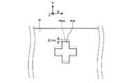
図8は、第1実施形態に係る基板の変形を説明する説明図である。露光装置EXでは、第2ドラム部材22に接触した基板Pに緩みがある場合、基板Pにしわが発生する可能性がある。このため露光装置EXでは、基板Pの搬送時に基板に張力(テンション)がかかるようにしている。図8に示すように、基板Pに張力(テンション)がかかる場合、第2ドラム部材22の曲面に進入する前に、基板PのY方向の端部が弓状に湾曲し、張力(テンション)の影響による基板Pの幅方向の変形Pwが発生する可能性がある。図9は、アライメントマークの一例を説明図である。図8に示すアライメント顕微鏡AMG1は、第2ドラム部材22のY方向の両側端の検出プローブで、搬送方向αに沿って図9に示す基板Pの両端付近に形成されたアライメントマークmaを常時観察または検出することができる。図9に示すように、基板Pは幅方向が同一の長尺のシートであることが多い。
FIG. 8 is an explanatory diagram illustrating deformation of the substrate according to the first embodiment. In the exposure apparatus EX, if there is a looseness in the substrate P that is in contact with the
図8に示すように、基板Pに張力(テンション)がかかる場合、第2ドラム部材22の曲面に進入する進入位置(接触し始める位置)IAからアライメント顕微鏡AMG1の顕微鏡視野(撮像範囲)までの所定距離QLが、例えば、数cm程度であれば、基板Pの本来の幅PPに近づくことができる。このように、進入位置IAでは、基板Pに付与される張力(テンション)と第2ドラム部材22の外周面の摩擦係数等により基板Pに変形が生じている可能性があるが、進入位置IAから所定距離QL離れた位置であれば、基板Pと第2ドラム部材22とが密着し、基板Pにかかる張力(テンション)が均等にかかり、基板Pの変形が安定した状態に収まることになる。
As shown in FIG. 8, when tension is applied to the substrate P, from the entry position (position where the contact starts) IA entering the curved surface of the
図10は、基板の変形によるアライメントマークの変化の一例を模式的に説明する説明図である。図11は、投影像とアライメントマークとの位置ずれを模式的に説明する説明図である。図12は、第1実施形態に係る処理装置(露光装置)の処理を補正する手順の一例を示すフローチャートである。図10に示すように、アライメント顕微鏡AMG1は、第1検出プローブとして、検出方向AM1にある顕微鏡視野(撮像範囲)mam1の範囲内でアライメントマークmaを検出する。同様に、アライメント顕微鏡AMG2は、第2検出プローブとして、検出方向AM2にある顕微鏡視野(撮像範囲)mam2の範囲内でアライメントマークmaを検出する。このようにアライメント顕微鏡AMG1及びアライメント顕微鏡AMG2は、図10に示す基板P上の特定パターンであるアライメントマークmaを検出する(ステップS11)。アライメント顕微鏡AMG1は、アライメントマークmaの撮像を制御装置14に出力し、制御装置14及びアライメント顕微鏡AMG1は、第1パターン検出装置として、アライメントマークmaを撮像データとして制御装置14の記憶部に記憶する。アライメント顕微鏡AMG2は、アライメントマークmaの撮像を制御装置14に出力し、制御装置14及びアライメント顕微鏡AMG2は、第2パターン検出装置として、アライメントマークmaを撮像データとして制御装置14の記憶部に記憶する。
FIG. 10 is an explanatory diagram schematically illustrating an example of a change in the alignment mark due to deformation of the substrate. FIG. 11 is an explanatory view for schematically explaining the positional deviation between the projected image and the alignment mark. FIG. 12 is a flowchart illustrating an example of a procedure for correcting processing of the processing apparatus (exposure apparatus) according to the first embodiment. As shown in FIG. 10, the alignment microscope AMG1 detects the alignment mark ma as a first detection probe within the range of the microscope visual field (imaging range) mam1 in the detection direction AM1. Similarly, the alignment microscope AMG2 detects the alignment mark ma as a second detection probe within the range of the microscope visual field (imaging range) mam2 in the detection direction AM2. Thus, alignment microscope AMG1 and alignment microscope AMG2 detect alignment mark ma which is a specific pattern on substrate P shown in FIG. 10 (step S11). The alignment microscope AMG1 outputs the image of the alignment mark ma to the
次に、エンコーダヘッドEN4の位置情報に紐付けて記憶部に記憶した、顕微鏡視野(撮像範囲)mam1のアライメントマークmaの撮像データと同じアライメントマークmaを、エンコーダヘッドEN5の位置情報から顕微鏡視野(撮像範囲)mam2で検出したアライメントマークmaとして検出し、撮像データ同士を比較する。例えば、制御装置14は、顕微鏡視野(撮像範囲)mam1のアライメントマークmaの撮像データから、基板Pの幅方向(Y方向)のアライメントマークmaの間隔WY1を演算する。そして、演算装置14は、顕微鏡視野(撮像範囲)mam1のアライメントマークmaの撮像データと同じアライメントマークmaを、エンコーダヘッドEN5の位置情報から顕微鏡視野(撮像範囲)mam2で検出し、撮像データから、基板Pの幅方向(Y方向)のアライメントマークmaの間隔WY2を演算する。間隔WY2と間隔WY1との差が記憶部に予め記憶した許容値以内であり、基板Pの変形によるアライメントマークmaの撮像データに変化がない場合(ステップS12、No)、制御装置14は、ステップS11の処理を実行する。間隔WY2と間隔WY1との差が記憶部に予め記憶した許容値を超えており、基板Pの変形によるアライメントマークmaの撮像データに変化がある場合(ステップS12、Yes)、制御装置14は、ステップS13に処理を進める。
Next, the alignment mark ma which is the same as the imaging data of the alignment mark ma of the microscope field of view (imaging range) mam, stored in the storage unit in association with the position information of the encoder head EN4, is obtained from the position information of the encoder head EN5. Imaging range) Detected as alignment mark ma detected at mam2, and the imaging data are compared with each other. For example, the
あるいは、エンコーダヘッドEN4の位置情報に紐付けて記憶部に記憶した、顕微鏡視野(撮像範囲)mam1のアライメントマークmaの撮像データと同じアライメントマークmaを、エンコーダヘッドEN5の位置情報から顕微鏡視野(撮像範囲)mam2で検出したアライメントマークmaとして検出し、撮像データ同士を比較する。ここで、アライメント顕微鏡AMG1は、露光された投影像masを検出できる。その為に、アライメント顕微鏡AMG1は、例えば位相差顕微鏡または偏光顕微鏡とされる。位相差顕微鏡または偏光顕微鏡は、例えばレジスト材料が光を受けて材料の屈折率を変化させる場合、屈折率の変化をコントラストの差として検出し、現像前に露光状態を潜像として検出できる。この場合、図11に示す、アライメントマークmamと同じ形状の投影像を露光した場合、潜像形状の投影像masもアライメントマークmamと相似の形状となる。この潜像形状の投影像masとアライメントマークmaとの撮像データに変化がない場合(ステップS12、No)、制御装置14は、ステップS11の処理を実行する。図11に示す、投影像masとアライメントマークmaとの撮像データに変化Δmsがある場合(ステップS12、Yes)、制御装置14は、ステップS13に処理を進めるようにしてもよい。
Alternatively, the same alignment mark ma as the imaging data of the alignment mark ma of the microscope field of view (imaging range)
次に、露光装置EXは、第1ガイド部材32及び第2ガイド部材33の位置を調整し、第1検出プローブであるアライメント顕微鏡AMG1が検出したアライメントマークma(特定パターン)により求めた第2中心軸AX2と平行な軸方向の基板Pの変形量と、第2検出プローブであるアライメント顕微鏡AMG2が検出したアライメントマークma(特定パターン)により求めた前記軸方向の基板Pの変形量と、が一致するように進入位置IA及び離脱位置OAを第2ドラム部材22の周囲に設定し、基板Pを案内する。露光装置EXは、図1に示すEPC、搬送装置9の搬送する搬送方向を調整してもよい。
Next, the exposure apparatus EX adjusts the positions of the
図2に示す特定位置PXを第1検出プローブであるアライメント顕微鏡AMG1が配置されている位置に第2中心軸AX2の軸回りに回転した角度とほぼ同じ角度だけ、第2中心軸AX2からみて特定位置PXよりも離脱位置OA側に回転した前記基板支持部材の周囲の位置に、第2検出プローブであるアライメント顕微鏡AMG2が配置されているので、アライメント顕微鏡AMG1が検出したアライメントマークma(特定パターン)により求めた第2中心軸AX2と平行な軸方向の基板Pの変形量と、アライメント顕微鏡AMG1が検出したアライメントマークma(特定パターン)により求めた前記軸方向の基板Pの変形量とが一致すれば、第2ドラム部材22に巻き付いている基板Pは安定しているものと推定できる。このため、露光装置EXは、第1特定位置PX1、特定位置PXまたは第2特定位置PX2において、露光光を照射する処理を精密に行うことができる。
The specific position PX shown in FIG. 2 is specified as viewed from the second central axis AX2 by the same angle as the angle rotated about the second central axis AX2 at the position where the alignment microscope AMG1 as the first detection probe is arranged. Since the alignment microscope AMG2 as the second detection probe is arranged at a position around the substrate support member rotated to the separation position OA side from the position PX, the alignment mark ma (specific pattern) detected by the alignment microscope AMG1 The amount of deformation of the substrate P in the axial direction parallel to the second central axis AX2 obtained by the above-mentioned is coincident with the amount of deformation of the substrate P in the axial direction obtained by the alignment mark ma (specific pattern) detected by the alignment microscope AMG1. In this case, it can be estimated that the substrate P wound around the
露光装置EXは、演算装置14が顕微鏡視野(撮像範囲)mam1のアライメントマークmaの撮像データと同じアライメントマークmaを、エンコーダヘッドEN5の位置情報から顕微鏡視野(撮像範囲)mam2で検出し、撮像データから、基板Pの幅方向(Y方向)の変形量を演算できる。上述した像シフト調整装置は、基板Pの幅方向(Y方向)の変形量に応じて、投影像の位置をシフトする、投影像の補正を行う(ステップS13)。または、露光装置EXは、上述した倍率調整装置が、基板Pの幅方向(Y方向)の変形量に応じて、投影像の倍率を補正する、投影像の補正を行ってもよい。あるいは、露光装置EXは、上述した倍率調整装置及び像シフト調整装置が、基板Pの幅方向(Y方向)の変形量に応じて、投影像のシフト及び倍率を補正する、投影像の補正を行ってもよい。
In the exposure apparatus EX, the
(第2実施形態)
次に、本発明に係る処理装置の第2実施形態について、図13、図14及び図15を参照して説明する。図13は、第2実施形態に係る処理装置(露光装置)のアライメントマークの検出手順の一例を示すフローチャートである。図14は、アライメントマークの検出位置の一例を示す説明図である。図15は、アライメントマークの検出位置の他の例を示す説明図である。この図において、第1実施形態の構成要素と同一の要素については同一符号を付し、その説明を省略する。露光装置EXは、露光を精度よく実行するために、上述した基板P上のアライメントマークmaをできるだけ多く検出し、多くの検出データを用いて投影像の補正を行うことが望ましい。しかしながら、演算装置14には、多くの検出データを用いて演算する演算負荷がかかることになる。上述したように、例えば、アライメント顕微鏡AMG1で検出した基板Pのアライメントマークmaが、搬送されて、図2に示す第1特定位置PX1に達するまでに、制御装置14は、投影像のシフト及び倍率の少なくとも1つを補正する、投影像の補正のための補正データを演算し終わり、像シフト調整装置及び倍率調整装置の少なくとも1つを制御する必要がある。このため、搬送装置9は、基板Pを搬送できる搬送速度を増加させると、制御装置14は、投影像のシフト及び倍率の少なくとも1つを補正するための補正データを演算し終わらない可能性がある。そこで、搬送装置9による基板Pの搬送速度を低下させる(同時に円筒マスクDMの回転速度も低下させる)場合、露光装置EXのスループットまたはデバイス製造システム1のスループットが低下する可能性がある。
(Second Embodiment)
Next, a second embodiment of the processing apparatus according to the present invention will be described with reference to FIG. 13, FIG. 14, and FIG. FIG. 13 is a flowchart illustrating an example of an alignment mark detection procedure of the processing apparatus (exposure apparatus) according to the second embodiment. FIG. 14 is an explanatory diagram showing an example of the detection position of the alignment mark. FIG. 15 is an explanatory diagram illustrating another example of the detection position of the alignment mark. In this figure, the same reference numerals are given to the same elements as those of the first embodiment, and the description thereof is omitted. It is desirable that the exposure apparatus EX detects as many alignment marks ma on the substrate P as described above as much as possible in order to perform exposure with high accuracy, and corrects the projected image using a large amount of detection data. However, the
図13に示すように、制御装置14は、上述した処理部の基板Pに光を照射する照射処理を停止した状態とする(ステップS21)。次に、搬送装置9は、処理部が処理を停止した状態で基板Pを移動させ、バッファー部DLへ搬送する(ステップS22)。搬送装置9は、搬送速度を低速とし、第1パターン検出装置または第2パターン検出装置に多くのアライメントマークmaを検出可能にさせる時間を与える。次に、上述した少なくとも第1パターン検出装置が特定パターンであるアライメントマークmaを検出する。または、処理部にアライメントマークmaのみへの露光を行わせ第2パターン検出装置がアライメントマークmaへの露光のずれを検出してもよい。そして、制御装置14は、特定パターンであるアライメントマークmaを撮像データとして制御装置14の記憶部に記憶する(ステップS23)。このとき、制御装置14は、後述する一部のアライメントマークmaを取り込む場合に、取り込まなかったアライメントマークmaを補完する補正データを演算し、記憶部に保存しておく。
As shown in FIG. 13, the
次に、搬送装置9は、バッファー部DLからバックバッファー部BDLへ、処理部が処理を停止した状態で基板Pを移動させ、基板Pを逆移動させる(ステップS24)。搬送装置9は、上述したステップS22開始の位置である初期位置に基板が戻らない場合(ステップS25、No)、初期位置へ基板を逆移動させる処理(ステップS24)を継続する。搬送装置9は、基板Pが初期位置に戻った場合(ステップS25、Yes)、基板Pを処理装置U4へ向けて供給するように基板Pを移動する(ステップS26)。 Next, the transfer device 9 moves the substrate P from the buffer unit DL to the back buffer unit BDL in a state where the processing unit stops processing, and reversely moves the substrate P (step S24). When the substrate does not return to the initial position, which is the start position of Step S22 described above (No at Step S25), the transfer device 9 continues the process of moving the substrate back to the initial position (Step S24). When the substrate P returns to the initial position (step S25, Yes), the transfer device 9 moves the substrate P so as to supply the substrate P toward the processing device U4 (step S26).
上述した第1パターン検出装置及び第2パターン検出装置は、搬送装置9が移動させた基板Pのアライメントマークmaの一部を検出する(ステップS27)。制御装置14は、上述した処理部の基板Pに光を照射する照射処理を開始する(ステップS28)。例えば、図14に示すように、検出したアライメントマークmaをma1、検出していないアライメントマークmaをma2とする場合、検出したアライメントマークma1は、検出していないアライメントマークma2を挟み、1つ飛ばしでアライメント顕微鏡AMG1、AMG2が検出している。
The first pattern detection device and the second pattern detection device described above detect a part of the alignment mark ma of the substrate P moved by the transport device 9 (step S27). The
検出していないアライメントマークma2は、所定個数であればよく、例えば図15に示すように、搬送方向αに4つ並んでもよい。これにより、第1パターン検出装置及び第2パターン検出装置は、アライメントマークmaの一部のみを取り込むのでデータ処理の負荷を間引くことができ、制御装置14の演算負荷を抑制することができる。制御装置14は、上述した補正データを用いて、処理部に処理をさせる。このため、搬送装置9が搬送速度を増加しても、アライメント顕微鏡AMG1で検出した基板Pのアライメントマークmaが、搬送されて、図2に示す第1特定位置PX1に達するまでに、制御装置14は、投影像のシフト及び倍率の少なくとも1つを補正する、投影像の補正のための補正データを演算し終わることができる。制御装置14が上述した投影像の補正の演算をする時間を短縮し、処理することができる。その結果、基板搬送装置9は、基板Pの搬送速度を増加させ、露光装置EXは、スループットを向上させることができる。
The number of alignment marks ma2 that are not detected may be a predetermined number, and for example, four alignment marks ma2 may be arranged in the transport direction α as shown in FIG. Thereby, since the first pattern detection device and the second pattern detection device capture only a part of the alignment mark ma, the data processing load can be thinned out, and the calculation load on the
または、第1パターン検出装置及び第2パターン検出装置は、搬送装置9が移動させた基板Pのアライメントマークmaの全部を検出する。制御装置14が、アライメントマークmaを認識する画像処理をする場合、演算負荷がかかる。そこで、例えば、制御装置14が、図14に示すように、制御装置14が処理したアライメントマークmaの検出データをma1、制御装置14が画像処理していないアライメントマークmaをma2とする場合、制御装置14が画像処理したアライメントマークma1は、制御装置14が画像処理していないアライメントマークma2を挟み、1つ飛ばしでアライメント顕微鏡AMG1、AMG2が検出している。制御装置14が画像処理していないアライメントマークma2は、所定個数であればよく、例えば図15に示すように、搬送方向αに4つ並んでもよい。これにより、第1パターン検出装置及び第2パターン検出装置は、アライメントマークmaを検出するが、画像処理して取り込むデータ処理を間引く。その結果、露光装置EXは、制御装置14の負荷を抑制することができる。このため、搬送装置9が搬送速度を増加しても、アライメント顕微鏡AMG1で検出した基板Pのアライメントマークmaが、搬送されて、図2に示す第1特定位置PX1に達するまでに、制御装置14は、投影像のシフト及び倍率の少なくとも1つを補正する、投影像の補正のための補正データを演算し終わることができる。制御装置14が上述した投影像の補正の演算をする時間を短縮し、処理することができる。その結果、搬送装置9は、基板Pの搬送速度を増加させ、露光装置EXは、スループットを向上させることができる。
Alternatively, the first pattern detection device and the second pattern detection device detect all the alignment marks ma of the substrate P moved by the transport device 9. When the
なお、図13中のステップS25、S26では、基板Pを所定の搬送速度まで加速させる必要があり、その為の助走距離も含めて初期位置とする必要がある。また、基板Pの順方向(+α方向)への搬送中にアライメント顕微鏡AMG1、又はAMG2によって検出すべきアライメントマークmaを、例えば図14のように1つおきのアライメントマークma1とし、ステップS24で基板Pが逆方向(−α方向)に搬送される間は、未検出であったアライメントマークma2を順次検出するようにしても良い。その場合、基板Pの順方向(+α方向)搬送中に、少なくとも1つのアライメントマークma2を先に検出すること、或いは、基板Pの逆方向(−α方向)搬送中に、少なくとも1つのアライメントマークma1をダブって検出することによって、基板Pの搬送を順方向から逆方向へ切り替えた際に生じうる基板Pと第2ドラム部材22との間のすべり誤差等の影響を補正することができる。
In steps S25 and S26 in FIG. 13, it is necessary to accelerate the substrate P to a predetermined transport speed, and it is necessary to set the initial position including the running distance for that purpose. Further, the alignment mark ma to be detected by the alignment microscope AMG1 or AMG2 during the conveyance of the substrate P in the forward direction (+ α direction) is, for example, every other alignment mark ma1 as shown in FIG. While P is conveyed in the reverse direction (−α direction), alignment marks ma2 that have not been detected may be sequentially detected. In that case, at least one alignment mark ma2 is first detected during the forward transfer (+ α direction) of the substrate P, or at least one alignment mark is transferred during the reverse transfer (−α direction) of the substrate P. By detecting ma1 in a doubled manner, it is possible to correct an influence such as a slip error between the substrate P and the
(第3実施形態)
次に、本発明に係る処理装置の第3実施形態について、図16から図19を参照して説明する。図16は、第3実施形態に係る処理装置(露光装置)に適用される回転ドラムの斜視図である。図17は、第3実施形態に係るスケール円盤SDを回転中心線AX2方向にみた、読み取り装置の位置を説明するための説明図である。図18は、基板の変形によるアライメントマークの変化の一例を模式的に説明する説明図である。図19は、第3実施形態に係る処理装置(露光装置)の処理を補正する手順の一例を示すフローチャートである。この図において、第1実施形態及び第2実施形態の構成要素と同一の要素については同一符号を付し、その説明を省略する。
(Third embodiment)
Next, a third embodiment of the processing apparatus according to the present invention will be described with reference to FIGS. FIG. 16 is a perspective view of a rotating drum applied to a processing apparatus (exposure apparatus) according to the third embodiment. FIG. 17 is an explanatory diagram for explaining the position of the reading device when the scale disk SD according to the third embodiment is viewed in the direction of the rotation center line AX2. FIG. 18 is an explanatory diagram schematically illustrating an example of a change in the alignment mark due to the deformation of the substrate. FIG. 19 is a flowchart illustrating an example of a procedure for correcting processing of the processing apparatus (exposure apparatus) according to the third embodiment. In this figure, the same reference numerals are given to the same elements as those of the first embodiment and the second embodiment, and the description thereof is omitted.
第1実施形と同様に、本実施形態でも露光装置EXは、第2ドラム部材22の曲面に支持される基板Pの一部分に、図2に示す投影光学系PLにより投影されたマスクパターンの一部分の像と基板Pとを相対的に位置合せ(アライメント)するために、基板Pに予め形成されたアライメントマークmaを検出するアライメント顕微鏡AMG1、AMG2が設けられている。第3実施形態の露光装置EXは、後述するアライメント顕微鏡AMG3、AMG4をさらに備えている。
Similar to the first embodiment, also in this embodiment, the exposure apparatus EX uses a part of the mask pattern projected onto the part of the substrate P supported by the curved surface of the
第1実施形と同様に、制御装置14は、第1ガイド部材32及び第2ガイド部材33の位置を調整し、第1検出プローブであるアライメント顕微鏡AMG1が検出したアライメントマークma(特定パターン)により求めた第2中心軸AX2と平行な軸方向の基板Pの変形量と、第2検出プローブであるアライメント顕微鏡AMG2が検出したアライメントマークma(特定パターン)により求めた前記軸方向の基板Pの変形量とが一致するように進入位置IA及び離脱位置OAを第2ドラム部材22の周囲に設定し、基板Pを案内する。
As in the first embodiment, the
図16に示すように、アライメント顕微鏡AMG3は、第2ドラム部材22の曲面に支持される基板Pの一部分に、図2に示す投影光学系PLにより投影されたマスクパターンの一部分の像と基板Pとを相対的に位置合せ(アライメント)するために、基板Pに予め形成されたアライメントマークmaを検出するアライメント顕微鏡AMG1と同様のアライメント顕微鏡である。アライメント顕微鏡AMG3は、Y軸方向(基板Pの幅方向)に一列に並んだ複数(例えば4つ)の検出プローブを有している。アライメント顕微鏡AMG3は、第2ドラム部材22のY軸方向の両側端の検出プローブで、基板Pの両端付近に形成されたアライメントマークmaを常時観察または検出することができる。
As shown in FIG. 16, the alignment microscope AMG3 includes an image of a part of the mask pattern projected on the part of the substrate P supported by the curved surface of the
エンコーダヘッドEN6は、基板Pの搬送方向の後方側、つまり露光位置(投影領域)の手前に配置されており、基板Pの搬送方向の後方側に向かってエンコーダヘッドEN4の設置方位線Le4を回転中心線AX2の軸回りに回転した設置方位線Le6上に設定される。また、XZ面内かつ回転中心線AX2からみたときに、アライメント顕微鏡AMG3による基板Pの観察方向AM3(回転中心線AX2に向かう)の検出中心と同一方向となるように、スケール部GPの径方向に設定される設置方位線Le6上に、エンコーダヘッドEN6が配置されている。 The encoder head EN6 is arranged on the rear side in the transport direction of the substrate P, that is, before the exposure position (projection area), and rotates the installation direction line Le4 of the encoder head EN4 toward the rear side in the transport direction of the substrate P. It is set on the installation direction line Le6 rotated around the axis of the center line AX2. In addition, the radial direction of the scale portion GP is in the same direction as the center of detection of the observation direction AM3 of the substrate P by the alignment microscope AMG3 (toward the rotation center line AX2) when viewed from the rotation center line AX2 in the XZ plane. The encoder head EN6 is arranged on the installation azimuth line Le6.
図17に示すように、アライメント顕微鏡AMG3の検出プローブが第2中心軸AX2からみて第2ドラム部材22の周囲に配置され、エンコーダヘッドEN6が配置された位置と第2中心軸AX2とを結ぶ方向(設置方位線Le6)が、第2中心軸AX2とアライメント顕微鏡AMG3の検出領域とを結ぶ方向と一致するよう配置されている。このため、XZ面内かつ回転中心線AX2からみたときに、アライメント顕微鏡AM3は、図2に示す進入位置IAとアライメント顕微鏡AMG1との間、かつ第2ドラム部材22の周囲に配置されている。
As shown in FIG. 17, the detection probe of the alignment microscope AMG3 is disposed around the
図2に示す第1特定位置PX1は、図17に示す第2中心軸AX2からみた設置方位線Le1(結像光束EL2の主光線の方位線)の延長線上にあり、第1特定位置PX1を第3検出プローブであるアライメント顕微鏡AMG3が配置されている位置に第2中心軸AX2の軸回りに回転した角度γ1とほぼ同じ角度だけ、第2中心軸AX2からみて第1特定位置PX1よりも離脱位置OA側に回転した第2ドラム部材22の周囲の位置に、第2検出プローブであるアライメント顕微鏡AMG2が配置される。制御装置14は、第1ガイド部材32及び第2ガイド部材33の位置を調整し、第3検出プローブであるアライメント顕微鏡AMG3が検出したアライメントマークma(特定パターン)により求めた第2中心軸AX2と平行な軸方向の基板Pの変形量と、第2検出プローブであるアライメント顕微鏡AMG2が検出したアライメントマークma(特定パターン)により求めた前記軸方向の基板Pの変形量とが一致するように進入位置IA及び離脱位置OAを第2ドラム部材22の周囲に設定し、基板Pを案内してもよい。
The first specific position PX1 shown in FIG. 2 is on an extension line of the installation azimuth line Le1 (azimuth line of the principal ray of the imaging light beam EL2) viewed from the second central axis AX2 shown in FIG. 17, and the first specific position PX1 is Only the same angle as the angle γ1 rotated about the second central axis AX2 at the position where the alignment microscope AMG3 as the third detection probe is disposed is separated from the first specific position PX1 as viewed from the second central axis AX2. An alignment microscope AMG2, which is a second detection probe, is disposed at a position around the
図16に示すエンコーダヘッドEN7は、基板Pの搬送方向の前方側、つまり露光位置(投影領域)の後方に配置されており、基板Pの搬送方向の前方側に向かってエンコーダヘッドEN5の設置方位線Le5を回転中心線AX2の軸回りに回転した設置方位線Le7上に設定される。また、露光装置EXは、上述したアライメント顕微鏡AMG3と同じ構成のアライメント顕微鏡AMG4(不図示)を備えている。図17に示すように、XZ面内かつ回転中心線AX2からみたときに、アライメント顕微鏡AMG4による基板Pの観察方向AM4(回転中心線AX2に向かう)の検出中心と同一方向となるように、スケール部GPの径方向に設定される設置方位線Le7上に、エンコーダヘッドEN7が配置されている。 The encoder head EN7 shown in FIG. 16 is arranged on the front side in the transport direction of the substrate P, that is, on the rear side of the exposure position (projection region), and the installation direction of the encoder head EN5 toward the front side in the transport direction of the substrate P. The line Le5 is set on the installation direction line Le7 that is rotated around the axis of the rotation center line AX2. Further, the exposure apparatus EX includes an alignment microscope AMG4 (not shown) having the same configuration as the alignment microscope AMG3 described above. As shown in FIG. 17, when viewed from the rotation center line AX2 in the XZ plane, the scale is set to be in the same direction as the detection center AM4 of the substrate P observed by the alignment microscope AMG4 (toward the rotation center line AX2). An encoder head EN7 is disposed on an installation orientation line Le7 set in the radial direction of the part GP.
図2に示す第2特定位置PX2は、図17に示す第2中心軸AX2からみた設置方位線Le2(結像光束EL2の主光線の方位線)の延長線上にあり、第2特定位置PX2を第1検出プローブであるアライメント顕微鏡AMG1が配置されている位置に第2中心軸AX2の軸回りに回転した角度γ2とほぼ同じ角度だけ、第2中心軸AX2からみて第2特定位置PX2よりも離脱位置OA側に回転した第2ドラム部材22の周囲の位置に、第4検出プローブであるアライメント顕微鏡AMG4が配置される。制御装置14は、第1ガイド部材32及び第2ガイド部材33の位置を調整し、第1検出プローブであるアライメント顕微鏡AMG1が検出したアライメントマークma(特定パターン)により求めた第2中心軸AX2と平行な軸方向の基板Pの変形量と、第4検出プローブであるアライメント顕微鏡AMG4が検出したアライメントマークma(特定パターン)により求めた前記軸方向の基板Pの変形量とが一致するように進入位置IA及び離脱位置OAを第2ドラム部材22の周囲に設定し、基板Pを案内してもよい。
The second specific position PX2 shown in FIG. 2 is on an extension line of the installation azimuth line Le2 (the azimuth line of the principal ray of the imaging light beam EL2) viewed from the second central axis AX2 shown in FIG. 17, and the second specific position PX2 is At a position where the alignment microscope AMG1 which is the first detection probe is disposed, it is separated from the second specific position PX2 as viewed from the second central axis AX2 by an angle substantially the same as the angle γ2 rotated around the second central axis AX2. An alignment microscope AMG4, which is a fourth detection probe, is disposed at a position around the
例えば、アライメント顕微鏡AMG3は、アライメントマークmaの撮像を制御装置14に出力し、制御装置14及びアライメント顕微鏡AMG3は、第3パターン検出装置として、アライメントマークmaを撮像データとして制御装置14の記憶部に記憶する。アライメント顕微鏡AMG1は、アライメントマークmaの撮像を制御装置14に出力し、制御装置14及びアライメント顕微鏡AMG1は、第1パターン検出装置として、アライメントマークmaを撮像データとして制御装置14の記憶部に記憶する。このため、図17に示す、第2ドラム部材22の曲面に進入する進入位置IAからアライメント顕微鏡AMG1の顕微鏡視野(撮像範囲)mam1までの距離を所定距離QL1とし、アライメント顕微鏡AMG1からアライメント顕微鏡AMG3の顕微鏡視野(撮像範囲)mam3までの距離を所定距離QL2とした場合、進入位置IAからアライメント顕微鏡AMG1の顕微鏡視野(撮像範囲)mam1までの所定距離QL=QL1+QL2となる。そして、アライメント顕微鏡AMG1及びアライメント顕微鏡AMG3は、図17に示す基板P上の特定パターンであるアライメントマークmaを検出する(図19のステップS31)。
For example, the alignment microscope AMG3 outputs the image of the alignment mark ma to the
次に、記憶部に記憶した、顕微鏡視野(撮像範囲)mam3のアライメントマークmaの撮像データと同じアライメントマークmaを、顕微鏡視野(撮像範囲)mam1で検出したアライメントマークmaと比較し撮像データ同士を比較する。例えば、制御装置14は、顕微鏡視野(撮像範囲)mam3のアライメントマークmaの撮像データから、基板Pの幅方向(Y方向)のアライメントマークmaの間隔WY3を演算する。なお、記憶部に記憶した、顕微鏡視野(撮像範囲)mam4のアライメントマークmaの撮像データと同じアライメントマークmaを、顕微鏡視野(撮像範囲)mam2で検出したアライメントマークmaと比較し撮像データ同士を比較する。例えば、制御装置14は、顕微鏡視野(撮像範囲)mam4のアライメントマークmaの撮像データから、基板Pの幅方向(Y方向)のアライメントマークmaの間隔WY4を演算してもよい。そして、演算装置14は、顕微鏡視野(撮像範囲)mam3のアライメントマークmaの撮像データと同じアライメントマークmaを、エンコーダヘッドEN4の位置情報から顕微鏡視野(撮像範囲)mam1で検出し、撮像データから、基板Pの幅方向(Y方向)のアライメントマークmaの間隔WY1を演算する。間隔WY3と間隔WY1との差Δmが記憶部に予め記憶した許容値以内であり、基板Pの変形によるアライメントマークmaの撮像データに変化がない場合(図19のステップS32が、No)、制御装置14は、図19のステップS31の処理を繰り返し実行する。間隔WY3と間隔WY1との差Δmが記憶部に予め記憶した許容値を超えており、基板Pの変形によるアライメントマークmaの撮像データに変化がある場合(図19のステップS32が、Yes)、制御装置14は、図19のステップS33に処理を進める。
Next, the same alignment mark ma as the imaging data of the alignment mark ma in the microscope field of view (imaging range) mam3 stored in the storage unit is compared with the alignment mark ma detected in the microscope field of view (imaging range) mam1, and the imaging data are compared. Compare. For example, the
次に、露光装置EXは、第1ガイド部材32及び第2ガイド部材33の位置を調整し、第1検出プローブであるアライメント顕微鏡AMG1が検出したアライメントマークma(特定パターン)により求めた第2中心軸AX2と平行な軸方向の基板Pの変形量と、第2検出プローブであるアライメント顕微鏡AMG2が検出したアライメントマークma(特定パターン)により求めた前記軸方向の基板Pの変形量と、が一致するように進入位置IA及び離脱位置OAを第2ドラム部材22の周囲に設定し、基板Pを案内する。例えば、制御装置14は、基板Pの幅方向における目標幅PPとなるように、搬送装置9を制御し、基板Pの搬送方向の速度を遅くする。
Next, the exposure apparatus EX adjusts the positions of the
なお、基板Pの幅方向の寸法を微小に変える為には、基板Pが第2ドラム部材22の外周面に進入(密着)する手前で、基板Pに幅方向の張力が付与されるようなローラ、例えば、回転軸方向について中央部の径が大きく(或いは小さく)、両端部側の径が小さい(或いは大きい)ローラ等を、例えば、図2中の回転ローラDR4として設けると良い。
その他、基板Pの幅方向の両端部の各々を、モータ駆動するニップローラで挟み込み、そのニップローラによる基板Pの送り方向を、本来の送り方向(基板長尺方向)に対して斜めにすることによって、基板Pの幅方向の両端部に共に外側に引っ張る力を与えて、基板Pを拡幅する構成としても良い。
In order to change the dimension in the width direction of the substrate P minutely, a tension in the width direction is applied to the substrate P before the substrate P enters (contacts) the outer peripheral surface of the
In addition, each of both ends in the width direction of the substrate P is sandwiched between nip rollers driven by a motor, and the feeding direction of the substrate P by the nip rollers is inclined with respect to the original feeding direction (the substrate long direction), The substrate P may be widened by applying a pulling force to both ends in the width direction of the substrate P.
図2に示す特定位置PXを第1検出プローブであるアライメント顕微鏡AMG1が配置されている位置に第2中心軸AX2の軸回りに回転した角度とほぼ同じ角度だけ、第2中心軸AX2からみて特定位置PXよりも離脱位置OA側に回転した前記基板支持部材の周囲の位置に、第2検出プローブであるアライメント顕微鏡AMG2が配置されているので、アライメント顕微鏡AMG1が検出したアライメントマークma(特定パターン)により求めた第2中心軸AX2と平行な軸方向の基板Pの変形量と、アライメント顕微鏡AMG1が検出したアライメントマークma(特定パターン)により求めた前記軸方向の基板Pの変形量とが一致すれば、第2ドラム部材22に巻き付いている基板Pは安定しているものと推定できる。このため、露光装置EXは、第1特定位置PX1、特定位置PXまたは第2特定位置PX2において、露光光を照射する処理を精密に行うことができる。
The specific position PX shown in FIG. 2 is specified as viewed from the second central axis AX2 by the same angle as the angle rotated about the second central axis AX2 at the position where the alignment microscope AMG1 as the first detection probe is arranged. Since the alignment microscope AMG2 as the second detection probe is arranged at a position around the substrate support member rotated to the separation position OA side from the position PX, the alignment mark ma (specific pattern) detected by the alignment microscope AMG1 The amount of deformation of the substrate P in the axial direction parallel to the second central axis AX2 obtained by the above-mentioned is coincident with the amount of deformation of the substrate P in the axial direction obtained by the alignment mark ma (specific pattern) detected by the alignment microscope AMG1. In this case, it can be estimated that the substrate P wound around the
露光装置EXは、演算装置14が顕微鏡視野(撮像範囲)mam1のアライメントマークmaの撮像データと同じアライメントマークmaを、エンコーダヘッドEN5の位置情報から顕微鏡視野(撮像範囲)mam2で検出し、撮像データから、基板Pの幅方向(Y方向)の変形量を演算できる。上述した像シフト調整装置は、基板Pの幅方向(Y方向)の変形量に応じて、投影像の位置をシフトする、投影像の補正を行う(ステップS13)。または、露光装置EXは、上述した倍率調整装置が、基板Pの幅方向(Y方向)の変形量に応じて、投影像の倍率を補正する、投影像の補正を行ってもよい。あるいは、露光装置EXは、上述した倍率調整装置及び像シフト調整装置が、基板Pの幅方向(Y方向)の変形量に応じて、投影像のシフト及び倍率を補正する、投影像の補正を行ってもよい。
In the exposure apparatus EX, the
(第4実施形態)
次に、本発明に係る処理装置の第4実施形態について、図20を参照して説明する。図20は、第4実施形態に係る処理装置(露光装置)の全体構成を示す模式図である。この図において、第1実施形態の構成要素と同一の要素については同一符号を付し、その説明を省略する。露光装置EX2は、光源から円筒マスクDMに照明される照明光束EL1を出射する。
(Fourth embodiment)
Next, a fourth embodiment of the processing apparatus according to the present invention will be described with reference to FIG. FIG. 20 is a schematic diagram showing an overall configuration of a processing apparatus (exposure apparatus) according to the fourth embodiment. In this figure, the same reference numerals are given to the same elements as those of the first embodiment, and the description thereof is omitted. The exposure apparatus EX2 emits an illumination light beam EL1 that illuminates the cylindrical mask DM from a light source.
光源装置13の光源から出射された照明光束EL1を照明モジュールILに導き、照明光学系が複数設けられている場合、光源からの照明光束EL1を複数に分離し、複数の照明光束EL1を複数の照明モジュールILに導く。
When the illumination light beam EL1 emitted from the light source of the
ここで、光源装置13から出射された照明光束EL1は、偏光ビームスプリッタSP1、SP2に入射する。偏光ビームスプリッタSP1、SP2では、照明光束EL1の分離によるエネルギーロスを抑制すべく、入射された照明光束EL1が全て反射するような光束にすることが好ましい。ここで、偏光ビームスプリッタSP1、SP2は、S偏光の直線偏光となる光束を反射し、P偏光の直線偏光となる光束を透過する。このため、光源装置13は、偏光ビームスプリッタSP1、SP2に入射する照明光束EL1が直線偏光(S偏光)の光束となる照明光束EL1を第1ドラム部材21に出射する。これにより、光源装置13は、波長及び位相が揃った照明光束EL1を出射する。
Here, the illumination light beam EL1 emitted from the
偏光ビームスプリッタSP1、SP2は、光源からの照明光束EL1を反射する一方で、円筒マスクDMで反射された結像光束(投影光束)EL2を透過している。換言すれば、照明モジュールILからの照明光束EL1は、偏光ビームスプリッタSP1、SP2に反射光束として入射し、円筒マスクDMからの結像光束EL2は、偏光ビームスプリッタSP1、SP2に透過光束として入射する。 The polarization beam splitters SP1 and SP2 reflect the illumination light beam EL1 from the light source and transmit the imaging light beam (projection light beam) EL2 reflected by the cylindrical mask DM. In other words, the illumination light beam EL1 from the illumination module IL enters the polarization beam splitters SP1 and SP2 as a reflected light beam, and the imaging light beam EL2 from the cylindrical mask DM enters the polarization beam splitters SP1 and SP2 as a transmitted light beam. .
このように処理部である照明モジュールILは、被処理物体である円筒マスクDM上の所定のパターン(マスクパターン)に照明光束EL1を反射させる処理を行う。これにより、投影光学系PLは、円筒マスクDM上の照明領域IRにおけるパターンの像を、搬送装置9によって搬送されている基板Pの一部(投影領域PA)に投影することができる。露光装置EX2は、円筒マスクDMで反射された投影光束により、第1特定位置PX1、第2特定位置PX2における基板Pに露光光を照射する処理をすることができる。 As described above, the illumination module IL as a processing unit performs a process of reflecting the illumination light beam EL1 to a predetermined pattern (mask pattern) on the cylindrical mask DM that is an object to be processed. Thereby, the projection optical system PL can project the image of the pattern in the illumination region IR on the cylindrical mask DM onto a part of the substrate P (projection region PA) being transported by the transport device 9. The exposure apparatus EX2 can perform a process of irradiating the substrate P at the first specific position PX1 and the second specific position PX2 with exposure light by the projected light beam reflected by the cylindrical mask DM.
(第5実施形態)
次に、本発明に係る処理装置の第5実施形態について、図21を参照して説明する。図21は、第5実施形態に係る処理装置(露光装置)の全体構成を示す模式図である。この図において、第1実施形態の構成要素と同一の要素については同一符号を付し、その説明を省略する。露光装置EX3は、ポリゴン走査ユニットPO1、PO2を備え、ポリゴン走査ユニットPOが、例えば紫外線のレーザ光原から射出されたビームをAOM等の変調器でパターンデータに応じて強度変調させたビームのスポット光を基板Pに向けて出射しつつ、そのスポット光を回転中心軸AX2と平行なY方向に一次元走査するスポット走査型描画装置であっても良い。
(Fifth embodiment)
Next, a fifth embodiment of the processing apparatus according to the present invention will be described with reference to FIG. FIG. 21 is a schematic diagram showing an overall configuration of a processing apparatus (exposure apparatus) according to the fifth embodiment. In this figure, the same reference numerals are given to the same elements as those of the first embodiment, and the description thereof is omitted. The exposure apparatus EX3 includes polygon scanning units PO1 and PO2, and the beam scanning spot is obtained by the polygon scanning unit PO, for example, intensity-modulating a beam emitted from an ultraviolet laser beam source with a modulator such as an AOM according to pattern data. It may be a spot scanning drawing apparatus that emits light toward the substrate P and performs one-dimensional scanning of the spot light in the Y direction parallel to the rotation center axis AX2.
このように、図21の露光装置EX3は、円筒マスクDMがなくても第1特定位置PX1、第2特定位置PX2における基板Pに露光光(スポット光)を照射する処理をすることができる。 As described above, the exposure apparatus EX3 in FIG. 21 can perform the process of irradiating the exposure light (spot light) onto the substrate P at the first specific position PX1 and the second specific position PX2 without the cylindrical mask DM.
(第6実施形態)
次に、本発明に係る処理装置の第6実施形態について、図22を参照して説明する。図22は、第6実施形態に係る処理装置(露光装置)の全体構成を示す模式図である。この図において、第1実施形態の構成要素と同一の要素については同一符号を付し、その説明を省略する。
(Sixth embodiment)
Next, a sixth embodiment of the processing apparatus according to the present invention will be described with reference to FIG. FIG. 22 is a schematic diagram showing an overall configuration of a processing apparatus (exposure apparatus) according to the sixth embodiment. In this figure, the same reference numerals are given to the same elements as those of the first embodiment, and the description thereof is omitted.
露光装置EX4は、所謂プロキシミティ露光を基板Pに施す処理装置である。露光装置EX4は、円筒マスクDMと、第2ドラム部材22との隙間を微小に設定して、照明機構IUが直接基板Pに照明光束ELを照射し、非接触露光する。本実施形態において、第2ドラム部材22は、電動モーター等のアクチュエータを含む第2駆動部36から供給されるトルクによって回転する。第2駆動部36の回転方向と逆回りとなるように、例えば磁気歯車で連結された駆動ローラMGGが第1ドラム部材21を駆動する。第2駆動部36は、第2ドラム部材22を回転するとともに、駆動ローラMGGと第1ドラム部材21とを連れ回し、第1ドラム部材21(円筒マスクDM)と第2ドラム部材22とを同期移動(同期回転)させる。
The exposure apparatus EX4 is a processing apparatus that performs so-called proximity exposure on the substrate P. In the exposure apparatus EX4, the gap between the cylindrical mask DM and the
また、露光装置EX4は、円筒マスクDMまたは基板Pに照射される照明光束ILの主光線が基板Pに入射する特定位置で、スケール部の位置PX6を検出するエンコーダヘッドEN8を備えている。ここで、第2ドラム部材22の外周面のうち基板Pが巻き付けられる外周面の直径と、スケール円盤のスケール部の直径とを揃えているので、位置PX8は、第2中心軸AX2からみて上述した特定位置と一致する。そして、エンコーダヘッドEN4は、基板Pの搬送方向の後方側に向かってエンコーダヘッドEN5の設置方位線Le5を回転中心線AX2の軸回りに、ほぼ90°回転した設置方位線Le4上に設定される。
In addition, the exposure apparatus EX4 includes an encoder head EN8 that detects the position PX6 of the scale portion at a specific position where the principal ray of the illumination light beam IL applied to the cylindrical mask DM or the substrate P is incident on the substrate P. Here, since the diameter of the outer peripheral surface around which the substrate P is wound out of the outer peripheral surfaces of the
本実施形態の露光装置EX4は、エンコーダヘッドEN5を第1読み取り装置とし、エンコーダヘッドEN4を第2読み取り装置とし、スケール部の読み取り出力から求めた、第2ドラム部材22の軸の位置と特定位置とを結び、かつ軸に直交する方向の変位の成分を、第1読み取り装置の読み取り出力で補正した処理を施すことができる。
The exposure apparatus EX4 of the present embodiment uses the encoder head EN5 as a first reading device, the encoder head EN4 as a second reading device, and the position and specific position of the axis of the
以上説明した第1から第6実施形態は、処理装置として露光装置を例示している。処理装置としては、露光装置に限られず、処理部がインクジェットのインク滴下装置により被処理物体である基板Pにパターンを印刷する装置であってもよい。または処理部は、検査装置であってもよい。 In the first to sixth embodiments described above, the exposure apparatus is exemplified as the processing apparatus. The processing apparatus is not limited to the exposure apparatus, and the processing unit may be an apparatus that prints a pattern on the substrate P, which is an object to be processed, using an inkjet ink dropping apparatus. Alternatively, the processing unit may be an inspection device.
(評価例)
ここで、基板Pが円筒状の第2ドラム部材22の外周面に一定角度で巻き付いている場合、基板Pが第2ドラム部材22と密着した部分での変形の程度を、図23に示したモデル例を用いてシミュレーションしてみる。図23において、第2ドラム部材22の回転中心軸AX2はY軸と平行とし、基板Pは第2ドラム部材22の外周面の上半分のほぼ180°に渡って巻き付けられているものとする。
(Evaluation example)
Here, when the substrate P is wound around the outer peripheral surface of the cylindrical
シミュレーションでは、基板Pの一端側を固定端、他端側を荷重端とし、荷重端に−Z方向の荷重(テンション)を一様に付与したときに、回転中心軸AX2の回りに回転可能な第2ドラム部材22の外周面上で、22.5度毎に設定した多数の点がどのように変位するかを求める。ここで、回転中心軸AX2と直交し、且つXZ面と平行な面内に、5本の線分ψ0、ψ−1、ψ−2、ψ+1、ψ+2を設定する。線分ψ0はZ軸と平行であり、線分ψ−1は線分ψ0に対して回転中心軸AX2の回りに−22.5°回転させたものであり、線分ψ+1は線分ψ0に対して回転中心軸AX2の回りに+22.5°回転させたものである。さらに、線分ψ−2は線分ψ0に対して回転中心軸AX2の回りに−45°回転させたものであり、線分ψ+2は線分ψ0に対して回転中心軸AX2の回りに+45°回転させたものである。
In the simulation, when one end side of the substrate P is a fixed end and the other end side is a load end, and a load (tension) in the −Z direction is uniformly applied to the load end, the substrate P can rotate around the rotation center axis AX2. It is determined how many points set every 22.5 degrees are displaced on the outer peripheral surface of the
また、基板P上の多数の対象点は、基板Pの幅方向(短尺方向であってY軸方向)の一端側の周方向の領域QA上、他端側の周方向の領域QB上、及び中央の周方向の領域QC上の各々に対して、5本の線分ψ0、ψ−1、ψ−2、ψ+1、ψ+2の各々に対応した計15ヶ所に設定される。例えば、中央の周方向の領域QC上で、線分ψ0の方向に位置する対象点は、QC(ψ0)で表わされ、一端側の周方向の領域QA上で、線分ψ+1の方向に位置する対象点は、QA(ψ+1)で表わされる。
また、基板Pの長尺方向をMD方向、短尺方向をTD方向とし、TD方向の正負はY軸の正負の方向と合わせる。
Further, a large number of target points on the substrate P are on the circumferential region QA on one end side in the width direction (short direction and Y-axis direction) of the substrate P, on the circumferential region QB on the other end side, and A total of 15 points corresponding to each of the five line segments ψ 0 , ψ −1 , ψ −2 , ψ +1 , ψ +2 are set for each of the central circumferential region QC. For example, the target point located in the direction of the line segment ψ 0 on the central circumferential region QC is represented by QC (ψ 0 ), and the line segment ψ +1 on the circumferential region QA on one end side. The target point located in the direction of is represented by QA (ψ +1 ).
Further, the long direction of the substrate P is the MD direction, the short direction is the TD direction, and the positive / negative of the TD direction is aligned with the positive / negative direction of the Y axis.
この図23のモデル例で、基板Pを厚さ100μmで30cm幅のPETとし、固定端はTD方向に一様にクランプした状態で、他端の荷重端にはMD方向に一様な張力(テンション)を掛けるものとする。その張力の大きさに応じて基板PはMD方向に伸びる。基板PのMD方向の伸縮に関しては、第2ドラム部材22が回転自在に支持されている為、第2ドラム部材22の外周面と基板Pの裏面との摩擦係数の大きさに余り影響されずに自由に伸縮する。
In the model example of FIG. 23, the substrate P is PET having a thickness of 100 μm and a width of 30 cm, the fixed end is uniformly clamped in the TD direction, and the load end at the other end is uniformly tensioned in the MD direction ( Tension). The substrate P extends in the MD direction according to the magnitude of the tension. Regarding the expansion and contraction of the substrate P in the MD direction, since the
図24は、摩擦係数μを0.45とした場合に、基板Pの領域QA上の5つの対象点QA(ψ−2)、QA(ψ−1)、QA(ψ0)、QA(ψ+1)、QA(ψ+2)、領域QB上の5つの対象点QB(ψ−2)、QB(ψ−1)、QB(ψ0)、QB(ψ+1)、QB(ψ+2)、及び、領域QC上の5つの対象点QC(ψ−2)、QC(ψ−1)、QC(ψ0)、QC(ψ+1)、QC(ψ+2)の各々が、張力(N)の変化に対してMD方向にどの程度変位するかをシミュレーションで求めたグラフである。 FIG. 24 shows five target points QA (ψ −2 ), QA (ψ −1 ), QA (ψ 0 ), QA (ψ) on the region QA of the substrate P when the friction coefficient μ is 0.45. +1 ), QA (ψ +2 ), five target points QB (ψ -2 ), QB (ψ -1 ), QB (ψ 0 ), QB (ψ +1 ), QB (ψ +2 ), and QB (ψ +2 ), and , Each of the five target points QC (ψ −2 ), QC (ψ −1 ), QC (ψ 0 ), QC (ψ +1 ), and QC (ψ +2 ) on the region QC changes in tension (N) It is the graph which calculated | required by how much it displaced to MD direction with respect to MD.
また、図25は、摩擦係数μを200とした場合に、基板Pの領域QA上の5つの対象点QA(ψ−2)〜QA(ψ+2)、領域QB上の5つの対象点QB(ψ−2)〜QB(ψ+2)、及び、領域QC上の5つの対象点QC(ψ−2)〜QC(ψ+2)の各々が、張力(N)の変化〔横軸〕に対してMD方向にどの程度変位するか〔縦軸〕をシミュレーションで求めたグラフである。 FIG. 25 shows five target points QA (ψ −2 ) to QA (ψ +2 ) on the region QA of the substrate P and five target points QB on the region QB (when the friction coefficient μ is 200). ψ -2) ~QB (ψ +2) , and each of the five target points on the region QC QC (ψ -2) ~QC ( ψ +2) is, with respect to a change in tension (N) [horizontal axis] It is the graph which calculated | required how much it displaced in MD direction [vertical axis] by simulation.
摩擦係数の大小に殆ど影響されず、各対象点は、グラフ中で斜線部で示した線形範囲内の値となった。斜線部の範囲で、最も大きい傾きを示した線形変化は、3つの領域QA、QB、QCの何れにおいても、線分ψ+2(+45°)の方向に位置する対象点QA(ψ+2)、QB(ψ+2)、QC(ψ+2)であった。また、斜線部の範囲で、最も小さい傾きを示した線形変化は、3つの領域QA、QB、QCの何れにおいても、線分ψ−2(−45°)の方向に位置する対象点QA(ψ−2)、QB(ψ−2)、QC(ψ−2)であった。 Each target point was a value within the linear range indicated by the shaded portion in the graph without being greatly affected by the magnitude of the friction coefficient. The linear change showing the greatest inclination in the shaded area is the target point QA (ψ +2 ) located in the direction of the line segment ψ +2 (+ 45 °) in any of the three regions QA, QB, and QC. QB (ψ +2 ) and QC (ψ +2 ). Further, the linear change indicating the smallest inclination in the shaded area is the target point QA (in the direction of the line segment ψ −2 (−45 °) in any of the three regions QA, QB, and QC. ψ -2 ), QB (ψ -2 ), and QC (ψ -2 ).
これに対して、基板PのTD方向の伸縮は、第2ドラム部材22の外周面と基板Pの裏面との摩擦係数の大きさに影響されて変化する。図26は、摩擦係数μを0.45とした場合に、領域QA上の5つの対象点QA(ψ−2)〜QA(ψ+2)、領域QB上の5つの対象点QB(ψ−2)〜QB(ψ+2)、及び、領域QC上の5つの対象点QC(ψ−2)〜QC(ψ+2)の各々が、張力(N)の変化に対してTD方向にどの程度変位するかをシミュレーションで求めたグラフである。
On the other hand, the expansion and contraction of the substrate P in the TD direction is changed by being influenced by the magnitude of the friction coefficient between the outer peripheral surface of the
また、図27は、摩擦係数μを200とした場合に、基板Pの領域QA上の5つの対象点QA(ψ−2)〜QA(ψ+2)、領域QB上の5つの対象点QB(ψ−2)〜QB(ψ+2)、及び、領域QC上の5つの対象点QC(ψ−2)〜QC(ψ+2)の各々が、張力(N)の変化〔横軸〕に対してTD方向にどの程度変位するか〔縦軸〕をシミュレーションで求めたグラフである。 FIG. 27 shows five target points QA (ψ −2 ) to QA (ψ +2 ) on the region QA of the substrate P and five target points QB ( ψ -2) ~QB (ψ +2) , and each of the five target points on the region QC QC (ψ -2) ~QC ( ψ +2) is, with respect to a change in tension (N) [horizontal axis] It is the graph which calculated | required how much it displaced in the TD direction [vertical axis] by simulation.
図26、27のグラフから判るように、基板PのTD方向の両側の領域QA、QBは、張力の増大に伴って基板Pの中央の領域QCに向けて変位する。即ち、基板PのTD方向の幅が縮まる方向に変形する。その変形量は、第2ドラム部材22の外周面と基板Pの裏面とのTD方向の摩擦係数の大小に応じて変わる。摩擦係数を0.45とした場合、基板Pは第2ドラム部材22の外周面上でTD方向に僅かにすべることができ、TD方向の収縮は比較的大きくなる。それに対して、摩擦係数を200とした場合、基板Pは第2ドラム部材22の外周面上でTD方向に殆どすべることができず、TD方向の収縮は比較的小さくなる。
As can be seen from the graphs of FIGS. 26 and 27, the regions QA and QB on both sides of the substrate P in the TD direction are displaced toward the center region QC of the substrate P as the tension increases. That is, the substrate P is deformed in a direction in which the width in the TD direction is reduced. The amount of deformation varies depending on the friction coefficient in the TD direction between the outer peripheral surface of the
以上のことから、基板Pの裏面と第2ドラム部材22の外周面との間の摩擦の大小と、MD方向の張力(テンション)の大小とによって、基板Pの第2ドラム部材22の外周面と密着している部分の概略的な変形の傾向や変形量を事前に予測することも可能となる。もちろん、基板Pの材質やプロセスを受けたか否か等によって、基板Pの剛性や摩擦係数が変わるため、それらも加味することで、より実用的な変形予測が可能となる。
From the above, the outer peripheral surface of the
従って、第1検出プローブが検出した特定パターンにより求めた回転中心軸AX2と平行な方向の基板Pの変形量と、第2検出プローブが検出した特定パターンにより求めた回転中心軸AXと平行な方向の基板Pの変形量とが一致するように、進入位置及び離脱位置を設定した位置に基板Pを案内するガイド部材が設けられる場合、そのガイド部材は、基板PのMD方向の張力(テンション)を調整するような搬送機構(ニップ方式の駆動ローラの回転制御やテンション調整用の回転ローラ等を含む)としても良い。 Accordingly, the deformation amount of the substrate P in the direction parallel to the rotation center axis AX2 obtained from the specific pattern detected by the first detection probe and the direction parallel to the rotation center axis AX obtained from the specific pattern detected by the second detection probe. When a guide member for guiding the substrate P is provided at a position where the entry position and the separation position are set so that the deformation amount of the substrate P matches, the guide member is a tension in the MD direction of the substrate P. It is also possible to use a conveyance mechanism (including a rotation control of a nip type driving roller and a rotation roller for tension adjustment).
<デバイス製造方法>
次に、図28を参照して、デバイス製造方法について説明する。図28は、第1実施形態に係る処理装置(露光装置)を用いたデバイス製造方法を示すフローチャートである。
<Device manufacturing method>
Next, a device manufacturing method will be described with reference to FIG. FIG. 28 is a flowchart showing a device manufacturing method using the processing apparatus (exposure apparatus) according to the first embodiment.
図28に示すデバイス製造方法では、まず、例えば有機EL等の自発光素子による表示パネルの機能・性能設計を行い、必要な回路パターンや配線パターンをCAD等で設計する(ステップS201)。次いで、CAD等で設計された各種レイヤー毎のパターンに基づいて、必要なレイヤー分の円筒マスクDMを製作する(ステップS202)。また、表示パネルの基材となる可撓性の基板P(樹脂フィルム、金属箔膜、プラスチック等)が巻かれた供給用ロールFR1を準備しておく、基板Pの製造を行う(ステップS203)。なお、このステップS203にて用意しておくロール状の基板Pは、必要に応じてその表面を改質したもの、下地層(例えばインプリント方式による微小凹凸)を事前形成したもの、光感応性の機能膜や透明膜(絶縁材料)を予めラミネートしたもの、でも良い。 In the device manufacturing method shown in FIG. 28, first, the function / performance design of a display panel using a self-luminous element such as an organic EL is performed, and necessary circuit patterns and wiring patterns are designed by CAD or the like (step S201). Next, a cylindrical mask DM for a necessary layer is manufactured based on the pattern for each layer designed by CAD or the like (step S202). Further, the substrate P is manufactured by preparing a supply roll FR1 around which a flexible substrate P (resin film, metal foil film, plastic, etc.) serving as a display panel base material is wound (step S203). . The roll-shaped substrate P prepared in step S203 has a surface modified as necessary, a pre-formed base layer (for example, micro unevenness by an imprint method), and light sensitivity. The functional film or transparent film (insulating material) previously laminated may be used.
次いで、基板P上に表示パネルデバイスを構成する電極や配線、絶縁膜、TFT(薄膜半導体)等によって構成されるバックプレーン層を形成すると共に、そのバックプレーンに積層されるように、有機EL等の自発光素子による発光層(表示画素部)が形成される(ステップS204)。このステップS204には、先の各実施形態で説明した露光装置EX、EX2、EX3、EX4を用いて、フォトレジスト層を露光する従来のフォトリソグラフィ工程も含まれるが、フォトレジストの代わりに感光性シランカップリング材を塗布した基板Pをパターン露光して表面に親撥水性によるパターンを形成する露光工程、光感応性の触媒層をパターン露光し、無電解メッキ法によってニッケル、銅、金等の金属膜のパターン(配線、電極等)を形成する湿式工程、或いは、銀ナノ粒子を含有した導電性インク等によってパターンを描画する印刷工程、等による処理も含まれる。 Next, a backplane layer composed of electrodes, wiring, insulating film, TFT (thin film semiconductor), etc. constituting the display panel device is formed on the substrate P, and an organic EL or the like is laminated on the backplane. A light emitting layer (display pixel portion) is formed by the self light emitting element (step S204). This step S204 includes a conventional photolithography process in which the photoresist layer is exposed using the exposure apparatuses EX, EX2, EX3, and EX4 described in the previous embodiments. The substrate P coated with the silane coupling material is subjected to pattern exposure to form a pattern based on hydrophilicity and water repellency on the surface, the photosensitive catalyst layer is subjected to pattern exposure, and nickel, copper, gold, etc. are formed by electroless plating. Processing by a wet process for forming a metal film pattern (wiring, electrode, etc.) or a printing process for drawing a pattern with a conductive ink containing silver nanoparticles is also included.
次いで、ロール方式で長尺の基板P上に連続的に製造される表示パネルデバイス毎に、基板Pをダイシングしたり、各表示パネルデバイスの表面に、保護フィルム(対環境バリア層)やカラーフィルターシート等を貼り合せたりして、デバイスを組み立てる(ステップS205)。次いで、表示パネルデバイスが正常に機能するか、所望の性能や特性を満たしているかの検査工程が行なわれる(ステップS206)。以上のようにして、表示パネル(フレキシブル・ディスプレイ)を製造することができる。 Next, the substrate P is diced for each display panel device continuously manufactured on the long substrate P by a roll method, or a protective film (environmental barrier layer) or a color filter is formed on the surface of each display panel device. A device is assembled by pasting sheets or the like (step S205). Next, an inspection process is performed to determine whether the display panel device functions normally or satisfies desired performance and characteristics (step S206). As described above, a display panel (flexible display) can be manufactured.
1 デバイス製造システム
2 基板供給装置
4 基板回収装置
5 上位制御装置
9 搬送装置
12 マスク保持装置
13 光源装置
14 制御装置
22 第2ドラム部材
DR1〜DR8 駆動ローラ
32 第1ガイド部材
33 第2ガイド部材
35 第2検出器
44 フォーカス補正光学部材
45 像シフト補正光学部材
46 ローテーション補正機構
47 倍率補正用光学部材
AMG1、AMG2、AMG3 アライメント顕微鏡
DM 円筒マスク
EN1、EN2、EN3、EN4、EN5 エンコーダヘッド
EX、EX2、EX3、EX4 露光装置(基板処理装置)
PO1、PO2 ポリゴン走査ユニット
DESCRIPTION OF
PO1, PO2 Polygon scanning unit
Claims (12)
前記基板を前記長尺方向に搬送する搬送装置と、
所定の軸から一定半径で湾曲した曲面を有し、前記基板の前記長尺方向の一部分が巻き付けられて、前記基板が前記曲面に接し始める前記長尺方向の進入位置から前記基板が前記曲面から離れ始める前記長尺方向の離脱位置までの前記基板を支持する基板支持部材と、
前記軸からみて前記基板支持部材の周囲に配置され、前記曲面の周方向のうちの特定位置で前記曲面にある前記基板に処理を施す処理部と、
前記特定パターンを検出する第1検出プローブを含み、前記周方向に関して前記特定位置と前記進入位置側との間の前記基板支持部材の周囲に前記第1検出プローブが配置される第1パターン検出装置と、
前記周方向に関して前記第1検出プローブと異なる位置で前記特定パターンを検出する第2検出プローブを含み、前記特定位置と前記第1検出プローブの位置との間の前記軸回りの回転角度とほぼ同じ角度だけ、前記周方向に関して前記特定位置よりも前記離脱位置側に回転した前記基板支持部材の周囲の位置に、前記第2検出プローブが配置される第2パターン検出装置と、
前記特定パターンの前記第1検出プローブによる検出で求められる前記基板の前記軸方向の変形量と、前記特定パターンの前記第2検出プローブによる検出で求められる前記基板の前記軸方向の変形量とが一致するように設定される前記進入位置及び前記離脱位置を通るように、前記搬送装置の一部として設けられて前記基板を案内するガイド部材と、
を備える
基板処理装置。 A substrate processing apparatus for processing a long substrate having flexibility in which a specific pattern is formed discretely or continuously in a long direction,
A transfer device for transferring the substrate to the elongated direction,
Has a curved surface which is curved at a constant radius from the predetermined axis, said length is wound longitudinal direction of a portion of the substrate, the substrate from the long direction of the entry position to start contacting the substrate to the curved surface from the curved surface a substrate support member supporting the substrate to the disengaged position of the elongated direction to start away,
Viewed from said axis is arranged around the substrate support member, and a processing unit which processes the substrate in said curved surface at a specific position of the circumferential direction of the curved surface,
A first pattern detection apparatus including a first detection probe for detecting the specific pattern, wherein the first detection probe is arranged around the substrate support member between the specific position and the entry position side in the circumferential direction. When,
It includes a second detection probe for detecting the specific pattern at a position different from the first detection probe with respect to the circumferential direction, about the same as the axis of the rotation angle between the position of the said specific position first detection probe A second pattern detection device in which the second detection probe is arranged at a position around the substrate support member rotated by an angle from the specific position with respect to the circumferential direction toward the separation position;
An amount of deformation of the substrate in the axial direction obtained by detection of the specific pattern by the first detection probe and an amount of deformation of the substrate in the axial direction obtained by detection of the specific pattern by the second detection probe. A guide member that is provided as a part of the transfer device and guides the substrate so as to pass through the entry position and the separation position that are set to coincide with each other ;
A substrate processing apparatus comprising:
前記ガイド部材は、
前記基板の搬送経路の前記進入位置の上流側で前記基板にテンションを付与すると共に、前記進入位置を前記曲面の周方向に調整するように移動する第1ガイド部材を含む、
基板処理装置。 The substrate processing apparatus according to claim 1,
The guide member is
Including a first guide member that applies tension to the substrate on the upstream side of the entry position of the substrate transport path and moves to adjust the entry position in the circumferential direction of the curved surface;
Substrate processing equipment.
前記ガイド部材は、
前記基板の搬送経路の前記離脱位置の下流側で前記基板にテンションを付与すると共に、前記離脱位置を前記曲面の周方向に調整するように移動する第2ガイド部材を含む、
基板処理装置。 The substrate processing apparatus according to claim 1 or 2, wherein
The guide member is
Including a second guide member that applies tension to the substrate on the downstream side of the separation position of the transport path of the substrate and moves to adjust the separation position in the circumferential direction of the curved surface,
Substrate processing equipment.
前記第1パターン検出装置の前記第1検出プローブは、前記軸方向に沿った複数の位置の各々に配置され、
前記第2パターン検出装置の前記第2検出プローブは、複数の前記第1検出プローブの前記軸方向の配置の間隔とほぼ同じ間隔で、前記軸方向に沿った複数の位置の各々に配置される、
基板処理装置。 A substrate processing apparatus according to any one of claims 1 to 3,
The first detection probe of the first pattern detection device is disposed at each of a plurality of positions along the axial direction,
The second detection probes of the second pattern detection device are arranged at each of a plurality of positions along the axial direction at substantially the same intervals as the axial arrangement intervals of the plurality of first detection probes. ,
Substrate processing equipment.
前記処理部は、前記特定位置において前記基板にパターンを形成する為の露光光を照射する露光装置である、
基板処理装置。 The substrate processing apparatus according to any one of claims 1 to 4, wherein
The processing unit is an exposure apparatus that irradiates exposure light for forming a pattern on the substrate at the specific position.
Substrate processing equipment.
前記露光装置は、前記露光光によって前記基板に形成されるパターン像の位置をシフトする像シフト調整装置を備え、
前記像シフト調整装置は、前記第1パターン検出装置及び前記第2パターン検出装置により検出された前記特定パターンの変化に応じて、前記パターン像の位置を前記長尺方向又は前記軸方向にシフトする、
基板処理装置。 The substrate processing apparatus according to claim 5,
The exposure apparatus includes an image shift adjustment device that shifts a position of a pattern image formed on the substrate by the exposure light,
The image shift adjustment device shifts the position of the pattern image in the longitudinal direction or the axial direction according to a change in the specific pattern detected by the first pattern detection device and the second pattern detection device. ,
Substrate processing equipment.
前記露光装置は、前記露光光によって前記基板に形成されるパターン像の倍率を調整する倍率調整装置を備え、
前記倍率調整装置は、前記第1パターン検出装置及び前記第2パターン検出装置により検出された前記特定パターンの変化に応じて、前記パターン像の倍率を調整する、
基板処理装置。 The substrate processing apparatus according to claim 5 or 6, wherein
The exposure apparatus includes a magnification adjustment device that adjusts a magnification of a pattern image formed on the substrate by the exposure light,
The magnification adjusting device adjusts the magnification of the pattern image according to a change in the specific pattern detected by the first pattern detecting device and the second pattern detecting device;
Substrate processing equipment.
前記基板支持部材は、
前記軸から一定半径の円筒面状の外周面を前記曲面として有して前記軸回りに回転する回転ドラムと、前記回転ドラムとともに前記軸回りに回転する読み取り可能な目盛が前記周方向に沿って刻設されたスケール部とを含み、
さらに、前記軸からみて前記スケール部の周囲であって、前記第1検出プローブが設置される方位と同じ方位に配置されて、前記スケール部の目盛を読み取る第1エンコーダヘッドと、
前記軸からみて前記スケール部の周囲であって、前記第2検出プローブが設置される方位と同じ方位に配置されて、前記スケール部の目盛を読み取る第2エンコーダヘッドと、
を備える、
基板処理装置。 A substrate processing apparatus according to any one of claims 1 to 7,
The substrate support member is
A rotating drum having a cylindrical outer peripheral surface having a constant radius from the shaft as the curved surface and rotating around the axis, and a readable scale rotating around the axis together with the rotating drum along the circumferential direction. Including the engraved scale part,
Furthermore, a first encoder head that is arranged around the scale portion as viewed from the axis and is arranged in the same orientation as the orientation in which the first detection probe is installed, and reads the scale of the scale portion;
A second encoder head arranged around the scale portion as viewed from the axis and arranged in the same orientation as the orientation in which the second detection probe is installed, and reads the scale of the scale portion;
Comprising
Substrate processing equipment.
前記第1パターン検出装置及び前記第2パターン検出装置は、
前記処理部が処理を停止した状態で、前記搬送装置及び前記回転ドラムの回転によって前記基板を前記長尺方向に所定の速度で移動させている間に、前記基板の前記特定パターンを検出する、
基板処理装置。 The substrate processing apparatus according to claim 8, comprising:
The first pattern detection device and the second pattern detection device are:
While the processing unit stops processing, the specific pattern of the substrate is detected while the substrate is moved at a predetermined speed in the longitudinal direction by rotation of the transfer device and the rotary drum .
Substrate processing equipment.
前記第1パターン検出装置及び前記第2パターン検出装置は、
前記搬送装置及び前記回転ドラムの回転によって前記基板を前記長尺方向に所定の速度で移動させながら、前記処理部によって処理を施している間も、前記基板上の前記長尺方向に沿った前記特定パターンの一部を検出する、
基板処理装置。 The substrate processing apparatus according to claim 8, comprising:
The first pattern detection device and the second pattern detection device are:
While the substrate is moved at a predetermined speed in the longitudinal direction by the rotation of the transfer device and the rotating drum, the processing unit is performing the processing by the processing unit , and the longitudinal direction along the longitudinal direction on the substrate. Detect part of a specific pattern,
Substrate processing equipment.
前記処理部は、
前記回転ドラムの周囲に配置され、前記曲面の周方向のうち前記特定位置で前記曲面にある前記基板に処理を施す第1処理部と、
前記回転ドラムの周囲に配置され、前記曲面の周方向のうち前記特定位置とは異なると共に、前記第1検出プローブの位置と前記第2検出プローブの位置との間に設定される第2の特定位置で、前記曲面にある前記基板に処理を施す第2処理部と、を含む、
基板処理装置。 The substrate processing apparatus according to claim 8, comprising:
The processor is
A first processing unit that is disposed around the rotating drum and that processes the substrate on the curved surface at the specific position in the circumferential direction of the curved surface;
A second specific position which is arranged around the rotating drum and which is different from the specific position in the circumferential direction of the curved surface and which is set between the position of the first detection probe and the position of the second detection probe. position, and a second processing unit which processes the substrate in the curved surface,
Substrate processing equipment.
前記処理部は、
前記回転ドラムの周囲に配置され、前記曲面の周方向のうち前記第1検出プローブの位置と前記第2検出プローブの位置との間に設定される第1の特定位置で、前記曲面にある前記基板に処理を施す第1処理部と、
前記回転ドラムの周囲に配置され、前記曲面の周方向のうち前記第1検出プローブの位置と前記第2検出プローブの位置との間で、且つ前記第1の特定位置とは異なる第2の特定位置で、前記曲面にある前記基板に処理を施す第2処理部と、を含み、
前記特定位置は、前記曲面の周方向に関して前記第1の特定位置と前記第2の特定位置との間に設定される、
基板処理装置。 The substrate processing apparatus according to claim 8, comprising:
The processor is
The first specific position, which is arranged around the rotating drum and is set between the position of the first detection probe and the position of the second detection probe in the circumferential direction of the curved surface, is on the curved surface. A first processing unit for processing a substrate;
A second identification that is arranged around the rotating drum and is different from the first identification position between the position of the first detection probe and the position of the second detection probe in the circumferential direction of the curved surface. A second processing unit for processing the substrate on the curved surface at a position;
The specific position is set between the first specific position and the second specific position with respect to a circumferential direction of the curved surface.
Substrate processing equipment.
Priority Applications (1)
| Application Number | Priority Date | Filing Date | Title |
|---|---|---|---|
| JP2014018844A JP6337486B2 (en) | 2014-02-03 | 2014-02-03 | Substrate processing equipment |
Applications Claiming Priority (1)
| Application Number | Priority Date | Filing Date | Title |
|---|---|---|---|
| JP2014018844A JP6337486B2 (en) | 2014-02-03 | 2014-02-03 | Substrate processing equipment |
Related Child Applications (1)
| Application Number | Title | Priority Date | Filing Date |
|---|---|---|---|
| JP2017228415A Division JP6500968B2 (en) | 2017-11-28 | 2017-11-28 | Substrate processing equipment |
Publications (3)
| Publication Number | Publication Date |
|---|---|
| JP2015145971A JP2015145971A (en) | 2015-08-13 |
| JP2015145971A5 JP2015145971A5 (en) | 2017-02-09 |
| JP6337486B2 true JP6337486B2 (en) | 2018-06-06 |
Family
ID=53890212
Family Applications (1)
| Application Number | Title | Priority Date | Filing Date |
|---|---|---|---|
| JP2014018844A Active JP6337486B2 (en) | 2014-02-03 | 2014-02-03 | Substrate processing equipment |
Country Status (1)
| Country | Link |
|---|---|
| JP (1) | JP6337486B2 (en) |
Cited By (1)
| Publication number | Priority date | Publication date | Assignee | Title |
|---|---|---|---|---|
| JP2019109546A (en) * | 2019-03-12 | 2019-07-04 | 株式会社ニコン | Substrate processing device |
Families Citing this family (4)
| Publication number | Priority date | Publication date | Assignee | Title |
|---|---|---|---|---|
| EP3358611B1 (en) * | 2015-09-29 | 2020-08-26 | Nikon Corporation | Production system |
| JP6551175B2 (en) * | 2015-11-10 | 2019-07-31 | 株式会社ニコン | Rotating cylindrical body measuring apparatus, substrate processing apparatus, and device manufacturing method |
| JP7148289B2 (en) * | 2018-06-20 | 2022-10-05 | 芝浦メカトロニクス株式会社 | Substrate detection device and substrate processing device |
| JP6787447B2 (en) * | 2019-06-27 | 2020-11-18 | 株式会社ニコン | Board processing equipment |
Family Cites Families (5)
| Publication number | Priority date | Publication date | Assignee | Title |
|---|---|---|---|---|
| US6018383A (en) * | 1997-08-20 | 2000-01-25 | Anvik Corporation | Very large area patterning system for flexible substrates |
| JP2008098325A (en) * | 2006-10-11 | 2008-04-24 | Nikon Corp | Exposure device and exposure method |
| JP6074898B2 (en) * | 2012-03-26 | 2017-02-08 | 株式会社ニコン | Substrate processing equipment |
| KR102077439B1 (en) * | 2012-03-26 | 2020-02-13 | 가부시키가이샤 니콘 | Pattern forming device |
| CN104246618B (en) * | 2012-04-19 | 2016-04-20 | 株式会社尼康 | Mask unit and substrate board treatment |
-
2014
- 2014-02-03 JP JP2014018844A patent/JP6337486B2/en active Active
Cited By (1)
| Publication number | Priority date | Publication date | Assignee | Title |
|---|---|---|---|---|
| JP2019109546A (en) * | 2019-03-12 | 2019-07-04 | 株式会社ニコン | Substrate processing device |
Also Published As
| Publication number | Publication date |
|---|---|
| JP2015145971A (en) | 2015-08-13 |
Similar Documents
| Publication | Publication Date | Title |
|---|---|---|
| JP6780742B2 (en) | Device manufacturing method | |
| TWI734360B (en) | Pattern forming apparatus | |
| JP6074898B2 (en) | Substrate processing equipment | |
| JP6337486B2 (en) | Substrate processing equipment | |
| TWI706234B (en) | Pattern forming device | |
| JP6123252B2 (en) | Processing apparatus and device manufacturing method | |
| JP6500968B2 (en) | Substrate processing equipment | |
| JP6658938B2 (en) | Substrate processing equipment | |
| JP6332482B2 (en) | Substrate processing equipment | |
| JP6252697B2 (en) | Substrate processing equipment | |
| JP6327305B2 (en) | Pattern exposure apparatus and device manufacturing method |
Legal Events
| Date | Code | Title | Description |
|---|---|---|---|
| A521 | Request for written amendment filed |
Free format text: JAPANESE INTERMEDIATE CODE: A523 Effective date: 20161221 |
|
| A621 | Written request for application examination |
Free format text: JAPANESE INTERMEDIATE CODE: A621 Effective date: 20161221 |
|
| A977 | Report on retrieval |
Free format text: JAPANESE INTERMEDIATE CODE: A971007 Effective date: 20170929 |
|
| A131 | Notification of reasons for refusal |
Free format text: JAPANESE INTERMEDIATE CODE: A131 Effective date: 20171010 |
|
| A521 | Request for written amendment filed |
Free format text: JAPANESE INTERMEDIATE CODE: A523 Effective date: 20171128 |
|
| TRDD | Decision of grant or rejection written | ||
| A01 | Written decision to grant a patent or to grant a registration (utility model) |
Free format text: JAPANESE INTERMEDIATE CODE: A01 Effective date: 20180410 |
|
| A61 | First payment of annual fees (during grant procedure) |
Free format text: JAPANESE INTERMEDIATE CODE: A61 Effective date: 20180423 |
|
| R150 | Certificate of patent or registration of utility model |
Ref document number: 6337486 Country of ref document: JP Free format text: JAPANESE INTERMEDIATE CODE: R150 |
|
| R250 | Receipt of annual fees |
Free format text: JAPANESE INTERMEDIATE CODE: R250 |
|
| R250 | Receipt of annual fees |
Free format text: JAPANESE INTERMEDIATE CODE: R250 |
|
| R250 | Receipt of annual fees |
Free format text: JAPANESE INTERMEDIATE CODE: R250 |