JP6332680B2 - Wiring board and manufacturing method thereof - Google Patents
Wiring board and manufacturing method thereof Download PDFInfo
- Publication number
- JP6332680B2 JP6332680B2 JP2014122705A JP2014122705A JP6332680B2 JP 6332680 B2 JP6332680 B2 JP 6332680B2 JP 2014122705 A JP2014122705 A JP 2014122705A JP 2014122705 A JP2014122705 A JP 2014122705A JP 6332680 B2 JP6332680 B2 JP 6332680B2
- Authority
- JP
- Japan
- Prior art keywords
- layer
- wiring
- insulating layer
- wiring layer
- metal plane
- Prior art date
- Legal status (The legal status is an assumption and is not a legal conclusion. Google has not performed a legal analysis and makes no representation as to the accuracy of the status listed.)
- Active
Links
Images


Classifications
-
- H—ELECTRICITY
- H01—ELECTRIC ELEMENTS
- H01L—SEMICONDUCTOR DEVICES NOT COVERED BY CLASS H10
- H01L23/00—Details of semiconductor or other solid state devices
- H01L23/48—Arrangements for conducting electric current to or from the solid state body in operation, e.g. leads, terminal arrangements ; Selection of materials therefor
- H01L23/488—Arrangements for conducting electric current to or from the solid state body in operation, e.g. leads, terminal arrangements ; Selection of materials therefor consisting of soldered or bonded constructions
- H01L23/498—Leads, i.e. metallisations or lead-frames on insulating substrates, e.g. chip carriers
- H01L23/49838—Geometry or layout
-
- H—ELECTRICITY
- H05—ELECTRIC TECHNIQUES NOT OTHERWISE PROVIDED FOR
- H05K—PRINTED CIRCUITS; CASINGS OR CONSTRUCTIONAL DETAILS OF ELECTRIC APPARATUS; MANUFACTURE OF ASSEMBLAGES OF ELECTRICAL COMPONENTS
- H05K3/00—Apparatus or processes for manufacturing printed circuits
- H05K3/0011—Working of insulating substrates or insulating layers
- H05K3/0044—Mechanical working of the substrate, e.g. drilling or punching
- H05K3/0047—Drilling of holes
-
- H—ELECTRICITY
- H01—ELECTRIC ELEMENTS
- H01L—SEMICONDUCTOR DEVICES NOT COVERED BY CLASS H10
- H01L21/00—Processes or apparatus adapted for the manufacture or treatment of semiconductor or solid state devices or of parts thereof
- H01L21/02—Manufacture or treatment of semiconductor devices or of parts thereof
- H01L21/04—Manufacture or treatment of semiconductor devices or of parts thereof the devices having at least one potential-jump barrier or surface barrier, e.g. PN junction, depletion layer or carrier concentration layer
- H01L21/48—Manufacture or treatment of parts, e.g. containers, prior to assembly of the devices, using processes not provided for in a single one of the subgroups H01L21/06 - H01L21/326
- H01L21/4814—Conductive parts
- H01L21/4846—Leads on or in insulating or insulated substrates, e.g. metallisation
- H01L21/4853—Connection or disconnection of other leads to or from a metallisation, e.g. pins, wires, bumps
-
- H—ELECTRICITY
- H01—ELECTRIC ELEMENTS
- H01L—SEMICONDUCTOR DEVICES NOT COVERED BY CLASS H10
- H01L21/00—Processes or apparatus adapted for the manufacture or treatment of semiconductor or solid state devices or of parts thereof
- H01L21/02—Manufacture or treatment of semiconductor devices or of parts thereof
- H01L21/04—Manufacture or treatment of semiconductor devices or of parts thereof the devices having at least one potential-jump barrier or surface barrier, e.g. PN junction, depletion layer or carrier concentration layer
- H01L21/48—Manufacture or treatment of parts, e.g. containers, prior to assembly of the devices, using processes not provided for in a single one of the subgroups H01L21/06 - H01L21/326
- H01L21/4814—Conductive parts
- H01L21/4846—Leads on or in insulating or insulated substrates, e.g. metallisation
- H01L21/4857—Multilayer substrates
-
- H—ELECTRICITY
- H01—ELECTRIC ELEMENTS
- H01L—SEMICONDUCTOR DEVICES NOT COVERED BY CLASS H10
- H01L21/00—Processes or apparatus adapted for the manufacture or treatment of semiconductor or solid state devices or of parts thereof
- H01L21/02—Manufacture or treatment of semiconductor devices or of parts thereof
- H01L21/04—Manufacture or treatment of semiconductor devices or of parts thereof the devices having at least one potential-jump barrier or surface barrier, e.g. PN junction, depletion layer or carrier concentration layer
- H01L21/50—Assembly of semiconductor devices using processes or apparatus not provided for in a single one of the subgroups H01L21/06 - H01L21/326, e.g. sealing of a cap to a base of a container
- H01L21/56—Encapsulations, e.g. encapsulation layers, coatings
- H01L21/563—Encapsulation of active face of flip-chip device, e.g. underfilling or underencapsulation of flip-chip, encapsulation preform on chip or mounting substrate
-
- H—ELECTRICITY
- H01—ELECTRIC ELEMENTS
- H01L—SEMICONDUCTOR DEVICES NOT COVERED BY CLASS H10
- H01L23/00—Details of semiconductor or other solid state devices
- H01L23/28—Encapsulations, e.g. encapsulating layers, coatings, e.g. for protection
- H01L23/31—Encapsulations, e.g. encapsulating layers, coatings, e.g. for protection characterised by the arrangement or shape
- H01L23/3157—Partial encapsulation or coating
- H01L23/3185—Partial encapsulation or coating the coating covering also the sidewalls of the semiconductor body
-
- H—ELECTRICITY
- H01—ELECTRIC ELEMENTS
- H01L—SEMICONDUCTOR DEVICES NOT COVERED BY CLASS H10
- H01L23/00—Details of semiconductor or other solid state devices
- H01L23/48—Arrangements for conducting electric current to or from the solid state body in operation, e.g. leads, terminal arrangements ; Selection of materials therefor
- H01L23/488—Arrangements for conducting electric current to or from the solid state body in operation, e.g. leads, terminal arrangements ; Selection of materials therefor consisting of soldered or bonded constructions
- H01L23/498—Leads, i.e. metallisations or lead-frames on insulating substrates, e.g. chip carriers
- H01L23/49811—Additional leads joined to the metallisation on the insulating substrate, e.g. pins, bumps, wires, flat leads
-
- H—ELECTRICITY
- H01—ELECTRIC ELEMENTS
- H01L—SEMICONDUCTOR DEVICES NOT COVERED BY CLASS H10
- H01L23/00—Details of semiconductor or other solid state devices
- H01L23/48—Arrangements for conducting electric current to or from the solid state body in operation, e.g. leads, terminal arrangements ; Selection of materials therefor
- H01L23/488—Arrangements for conducting electric current to or from the solid state body in operation, e.g. leads, terminal arrangements ; Selection of materials therefor consisting of soldered or bonded constructions
- H01L23/498—Leads, i.e. metallisations or lead-frames on insulating substrates, e.g. chip carriers
- H01L23/49822—Multilayer substrates
-
- H—ELECTRICITY
- H01—ELECTRIC ELEMENTS
- H01L—SEMICONDUCTOR DEVICES NOT COVERED BY CLASS H10
- H01L23/00—Details of semiconductor or other solid state devices
- H01L23/48—Arrangements for conducting electric current to or from the solid state body in operation, e.g. leads, terminal arrangements ; Selection of materials therefor
- H01L23/488—Arrangements for conducting electric current to or from the solid state body in operation, e.g. leads, terminal arrangements ; Selection of materials therefor consisting of soldered or bonded constructions
- H01L23/498—Leads, i.e. metallisations or lead-frames on insulating substrates, e.g. chip carriers
- H01L23/49833—Leads, i.e. metallisations or lead-frames on insulating substrates, e.g. chip carriers the chip support structure consisting of a plurality of insulating substrates
-
- H—ELECTRICITY
- H01—ELECTRIC ELEMENTS
- H01L—SEMICONDUCTOR DEVICES NOT COVERED BY CLASS H10
- H01L23/00—Details of semiconductor or other solid state devices
- H01L23/52—Arrangements for conducting electric current within the device in operation from one component to another, i.e. interconnections, e.g. wires, lead frames
- H01L23/538—Arrangements for conducting electric current within the device in operation from one component to another, i.e. interconnections, e.g. wires, lead frames the interconnection structure between a plurality of semiconductor chips being formed on, or in, insulating substrates
- H01L23/5386—Geometry or layout of the interconnection structure
-
- H—ELECTRICITY
- H01—ELECTRIC ELEMENTS
- H01L—SEMICONDUCTOR DEVICES NOT COVERED BY CLASS H10
- H01L23/00—Details of semiconductor or other solid state devices
- H01L23/552—Protection against radiation, e.g. light or electromagnetic waves
-
- H—ELECTRICITY
- H01—ELECTRIC ELEMENTS
- H01L—SEMICONDUCTOR DEVICES NOT COVERED BY CLASS H10
- H01L25/00—Assemblies consisting of a plurality of individual semiconductor or other solid state devices ; Multistep manufacturing processes thereof
- H01L25/03—Assemblies consisting of a plurality of individual semiconductor or other solid state devices ; Multistep manufacturing processes thereof all the devices being of a type provided for in the same subgroup of groups H01L27/00 - H01L33/00, or in a single subclass of H10K, H10N, e.g. assemblies of rectifier diodes
- H01L25/04—Assemblies consisting of a plurality of individual semiconductor or other solid state devices ; Multistep manufacturing processes thereof all the devices being of a type provided for in the same subgroup of groups H01L27/00 - H01L33/00, or in a single subclass of H10K, H10N, e.g. assemblies of rectifier diodes the devices not having separate containers
- H01L25/065—Assemblies consisting of a plurality of individual semiconductor or other solid state devices ; Multistep manufacturing processes thereof all the devices being of a type provided for in the same subgroup of groups H01L27/00 - H01L33/00, or in a single subclass of H10K, H10N, e.g. assemblies of rectifier diodes the devices not having separate containers the devices being of a type provided for in group H01L27/00
- H01L25/0655—Assemblies consisting of a plurality of individual semiconductor or other solid state devices ; Multistep manufacturing processes thereof all the devices being of a type provided for in the same subgroup of groups H01L27/00 - H01L33/00, or in a single subclass of H10K, H10N, e.g. assemblies of rectifier diodes the devices not having separate containers the devices being of a type provided for in group H01L27/00 the devices being arranged next to each other
-
- H—ELECTRICITY
- H05—ELECTRIC TECHNIQUES NOT OTHERWISE PROVIDED FOR
- H05K—PRINTED CIRCUITS; CASINGS OR CONSTRUCTIONAL DETAILS OF ELECTRIC APPARATUS; MANUFACTURE OF ASSEMBLAGES OF ELECTRICAL COMPONENTS
- H05K3/00—Apparatus or processes for manufacturing printed circuits
- H05K3/46—Manufacturing multilayer circuits
- H05K3/4602—Manufacturing multilayer circuits characterized by a special circuit board as base or central core whereon additional circuit layers are built or additional circuit boards are laminated
-
- H—ELECTRICITY
- H01—ELECTRIC ELEMENTS
- H01L—SEMICONDUCTOR DEVICES NOT COVERED BY CLASS H10
- H01L21/00—Processes or apparatus adapted for the manufacture or treatment of semiconductor or solid state devices or of parts thereof
- H01L21/02—Manufacture or treatment of semiconductor devices or of parts thereof
- H01L21/04—Manufacture or treatment of semiconductor devices or of parts thereof the devices having at least one potential-jump barrier or surface barrier, e.g. PN junction, depletion layer or carrier concentration layer
- H01L21/50—Assembly of semiconductor devices using processes or apparatus not provided for in a single one of the subgroups H01L21/06 - H01L21/326, e.g. sealing of a cap to a base of a container
- H01L21/60—Attaching or detaching leads or other conductive members, to be used for carrying current to or from the device in operation
- H01L2021/60007—Attaching or detaching leads or other conductive members, to be used for carrying current to or from the device in operation involving a soldering or an alloying process
- H01L2021/60022—Attaching or detaching leads or other conductive members, to be used for carrying current to or from the device in operation involving a soldering or an alloying process using bump connectors, e.g. for flip chip mounting
-
- H—ELECTRICITY
- H01—ELECTRIC ELEMENTS
- H01L—SEMICONDUCTOR DEVICES NOT COVERED BY CLASS H10
- H01L2224/00—Indexing scheme for arrangements for connecting or disconnecting semiconductor or solid-state bodies and methods related thereto as covered by H01L24/00
- H01L2224/01—Means for bonding being attached to, or being formed on, the surface to be connected, e.g. chip-to-package, die-attach, "first-level" interconnects; Manufacturing methods related thereto
- H01L2224/10—Bump connectors; Manufacturing methods related thereto
- H01L2224/15—Structure, shape, material or disposition of the bump connectors after the connecting process
- H01L2224/16—Structure, shape, material or disposition of the bump connectors after the connecting process of an individual bump connector
- H01L2224/161—Disposition
- H01L2224/16151—Disposition the bump connector connecting between a semiconductor or solid-state body and an item not being a semiconductor or solid-state body, e.g. chip-to-substrate, chip-to-passive
- H01L2224/16221—Disposition the bump connector connecting between a semiconductor or solid-state body and an item not being a semiconductor or solid-state body, e.g. chip-to-substrate, chip-to-passive the body and the item being stacked
- H01L2224/16225—Disposition the bump connector connecting between a semiconductor or solid-state body and an item not being a semiconductor or solid-state body, e.g. chip-to-substrate, chip-to-passive the body and the item being stacked the item being non-metallic, e.g. insulating substrate with or without metallisation
-
- H—ELECTRICITY
- H01—ELECTRIC ELEMENTS
- H01L—SEMICONDUCTOR DEVICES NOT COVERED BY CLASS H10
- H01L2224/00—Indexing scheme for arrangements for connecting or disconnecting semiconductor or solid-state bodies and methods related thereto as covered by H01L24/00
- H01L2224/01—Means for bonding being attached to, or being formed on, the surface to be connected, e.g. chip-to-package, die-attach, "first-level" interconnects; Manufacturing methods related thereto
- H01L2224/26—Layer connectors, e.g. plate connectors, solder or adhesive layers; Manufacturing methods related thereto
- H01L2224/31—Structure, shape, material or disposition of the layer connectors after the connecting process
- H01L2224/32—Structure, shape, material or disposition of the layer connectors after the connecting process of an individual layer connector
- H01L2224/321—Disposition
- H01L2224/32151—Disposition the layer connector connecting between a semiconductor or solid-state body and an item not being a semiconductor or solid-state body, e.g. chip-to-substrate, chip-to-passive
- H01L2224/32221—Disposition the layer connector connecting between a semiconductor or solid-state body and an item not being a semiconductor or solid-state body, e.g. chip-to-substrate, chip-to-passive the body and the item being stacked
- H01L2224/32225—Disposition the layer connector connecting between a semiconductor or solid-state body and an item not being a semiconductor or solid-state body, e.g. chip-to-substrate, chip-to-passive the body and the item being stacked the item being non-metallic, e.g. insulating substrate with or without metallisation
-
- H—ELECTRICITY
- H01—ELECTRIC ELEMENTS
- H01L—SEMICONDUCTOR DEVICES NOT COVERED BY CLASS H10
- H01L2224/00—Indexing scheme for arrangements for connecting or disconnecting semiconductor or solid-state bodies and methods related thereto as covered by H01L24/00
- H01L2224/73—Means for bonding being of different types provided for in two or more of groups H01L2224/10, H01L2224/18, H01L2224/26, H01L2224/34, H01L2224/42, H01L2224/50, H01L2224/63, H01L2224/71
- H01L2224/732—Location after the connecting process
- H01L2224/73201—Location after the connecting process on the same surface
- H01L2224/73203—Bump and layer connectors
- H01L2224/73204—Bump and layer connectors the bump connector being embedded into the layer connector
-
- H—ELECTRICITY
- H01—ELECTRIC ELEMENTS
- H01L—SEMICONDUCTOR DEVICES NOT COVERED BY CLASS H10
- H01L23/00—Details of semiconductor or other solid state devices
- H01L23/48—Arrangements for conducting electric current to or from the solid state body in operation, e.g. leads, terminal arrangements ; Selection of materials therefor
- H01L23/488—Arrangements for conducting electric current to or from the solid state body in operation, e.g. leads, terminal arrangements ; Selection of materials therefor consisting of soldered or bonded constructions
- H01L23/498—Leads, i.e. metallisations or lead-frames on insulating substrates, e.g. chip carriers
- H01L23/49827—Via connections through the substrates, e.g. pins going through the substrate, coaxial cables
-
- H—ELECTRICITY
- H01—ELECTRIC ELEMENTS
- H01L—SEMICONDUCTOR DEVICES NOT COVERED BY CLASS H10
- H01L2924/00—Indexing scheme for arrangements or methods for connecting or disconnecting semiconductor or solid-state bodies as covered by H01L24/00
- H01L2924/15—Details of package parts other than the semiconductor or other solid state devices to be connected
- H01L2924/151—Die mounting substrate
- H01L2924/1517—Multilayer substrate
- H01L2924/15192—Resurf arrangement of the internal vias
-
- H—ELECTRICITY
- H01—ELECTRIC ELEMENTS
- H01L—SEMICONDUCTOR DEVICES NOT COVERED BY CLASS H10
- H01L2924/00—Indexing scheme for arrangements or methods for connecting or disconnecting semiconductor or solid-state bodies as covered by H01L24/00
- H01L2924/15—Details of package parts other than the semiconductor or other solid state devices to be connected
- H01L2924/151—Die mounting substrate
- H01L2924/153—Connection portion
- H01L2924/1531—Connection portion the connection portion being formed only on the surface of the substrate opposite to the die mounting surface
- H01L2924/15311—Connection portion the connection portion being formed only on the surface of the substrate opposite to the die mounting surface being a ball array, e.g. BGA
-
- H—ELECTRICITY
- H05—ELECTRIC TECHNIQUES NOT OTHERWISE PROVIDED FOR
- H05K—PRINTED CIRCUITS; CASINGS OR CONSTRUCTIONAL DETAILS OF ELECTRIC APPARATUS; MANUFACTURE OF ASSEMBLAGES OF ELECTRICAL COMPONENTS
- H05K2201/00—Indexing scheme relating to printed circuits covered by H05K1/00
- H05K2201/09—Shape and layout
- H05K2201/09209—Shape and layout details of conductors
- H05K2201/095—Conductive through-holes or vias
- H05K2201/096—Vertically aligned vias, holes or stacked vias
-
- H—ELECTRICITY
- H05—ELECTRIC TECHNIQUES NOT OTHERWISE PROVIDED FOR
- H05K—PRINTED CIRCUITS; CASINGS OR CONSTRUCTIONAL DETAILS OF ELECTRIC APPARATUS; MANUFACTURE OF ASSEMBLAGES OF ELECTRICAL COMPONENTS
- H05K3/00—Apparatus or processes for manufacturing printed circuits
- H05K3/40—Forming printed elements for providing electric connections to or between printed circuits
- H05K3/42—Plated through-holes or plated via connections
- H05K3/422—Plated through-holes or plated via connections characterised by electroless plating method; pretreatment therefor
Description
本発明は、配線基板及びその製造方法に関する。 The present invention relates to a wiring board and a manufacturing method thereof.
従来、半導体素子などの電子部品を搭載するための配線基板がある。近年では、電子部品の高性能化に伴って、配線基板のさらなる高密度化及び多層化が進められている。 Conventionally, there is a wiring board for mounting electronic components such as semiconductor elements. In recent years, with higher performance of electronic components, wiring boards are being further densified and multilayered.
後述する予備的事項の欄で説明するように、配線基板では、微細な配線層のパターン間でのクロストークを抑制するために、配線層の上又は下に金属プレーン層が形成される。金属プレーン層の挿入によって、スタックドビア構造を有する多層配線の積層数が一層分増えるため、製造歩留りの低下及びコスト上昇を招く課題がある。 As will be described in the preliminary item section described later, in the wiring board, a metal plane layer is formed on or below the wiring layer in order to suppress crosstalk between patterns of fine wiring layers. The insertion of the metal plane layer further increases the number of stacked multilayer wirings having a stacked via structure, which causes a reduction in manufacturing yield and an increase in cost.
歩留りよく製造できると共に、コスト低減を図ることができる金属プレーン層を備えた配線基板及びその製造方法を提供することを目的とする。 It is an object of the present invention to provide a wiring board provided with a metal plane layer that can be manufactured with a high yield and cost reduction, and a manufacturing method thereof.
以下の開示の一観点によれば、配線間隔が狭い配線部と、前記配線部よりも配線間隔が広い配線部とを備えた第1配線層と、前記第1配線層の上に形成された第1絶縁層と、前記配線間隔が狭い配線部上の第1絶縁層の上に形成された金属プレーン層と、前記第1絶縁層及び前記金属プレーン層の上に形成された第2絶縁層と、前記第2絶縁層の上面から前記第1配線層に到達する第1ビアホールと、前記第1ビアホールに形成された第1ビア導体と、前記第2絶縁層に形成され、前記金属プレーン層に到達する第2ビアホールと、前記第2ビアホールに形成された第2ビア導体と、前記第2絶縁層の上に形成され、前記第1ビア導体を介して前記第1配線層に接続される第2配線層と、前記第2絶縁層の上に形成され、前記第2ビア導体を介して前記金属プレーン層に接続された第3配線層と、前記第2配線層の上に形成された第3絶縁層と、前記第3絶縁層に形成され、前記第2配線層に到達する第3ビアホールと、前記第3ビアホールに形成された第3ビア導体と、前記第3絶縁層の上に形成され、前記第3ビア導体を介して前記第2配線層に接続された第4配線層とを有し、前記第2配線層はビア受けパッドであり、前記第2配線層の上下に配置された前記第1ビア導体と前記第3ビア導体とによってスタックドビア構造が構築されている配線基板が提供される。 According to one aspect of the following disclosure, a first wiring layer including a wiring portion having a narrow wiring interval, a wiring portion having a wiring interval wider than the wiring portion, and the first wiring layer is formed on the first wiring layer A first insulating layer; a metal plane layer formed on the first insulating layer on the wiring portion having a narrow wiring interval; and a second insulating layer formed on the first insulating layer and the metal plane layer. A first via hole reaching the first wiring layer from an upper surface of the second insulating layer; a first via conductor formed in the first via hole; and the metal plane layer formed in the second insulating layer. A second via hole reaching the second via hole, a second via conductor formed in the second via hole, and formed on the second insulating layer, and connected to the first wiring layer via the first via conductor. A second wiring layer and a second insulating layer formed on the second insulating layer; A third wiring layer connected to the metal plane layer and a third insulating layer formed on the second wiring layer is formed on the third insulating layer to reach the second wiring layer A third via hole, a third via conductor formed in the third via hole, and a fourth wiring formed on the third insulating layer and connected to the second wiring layer via the third via conductor; Wiring in which a stacked via structure is constructed by the first via conductor and the third via conductor arranged above and below the second wiring layer, the second wiring layer being a via receiving pad. A substrate is provided.
また、その開示の他の観点によれば、配線間隔が狭い配線部と、前記配線部よりも配線間隔が広い配線部とを備えた第1配線層を含む配線部材を用意する工程と、前記第1配線層のパッド上に開口部が配置された第1絶縁層を形成する工程と、前記配線間隔が狭い配線部上の第1絶縁層の上に金属プレーン層を形成する工程と、前記第1絶縁層及び前記金属プレーン層の上に、前記第1絶縁層の開口部に第1ビアホールが配置され、前記金属プレーン層の上に第2ビアホールが配置された第2絶縁層を形成する工程と、前記第2絶縁層の上に、前記第1ビアホール内の第1ビア導体を介して前記第1配線層に接続される第2配線層と、前記第2ビアホール内の第2ビア導体を介して前記金属プレーン層に接続される第3配線層とを形成する工程と有する配線基板の製造方法が提供される。 Further, according to another aspect of the disclosure, a step of preparing a wiring member including a first wiring layer including a wiring portion having a narrow wiring interval and a wiring portion having a wiring interval wider than the wiring portion; Forming a first insulating layer having an opening on a pad of the first wiring layer; forming a metal plane layer on the first insulating layer on the wiring portion having a narrow wiring interval; and A second insulating layer is formed on the first insulating layer and the metal plane layer, the first via hole being disposed in the opening of the first insulating layer, and the second via hole being disposed on the metal plane layer. A second wiring layer connected to the first wiring layer via a first via conductor in the first via hole on the second insulating layer; and a second via conductor in the second via hole. Forming a third wiring layer connected to the metal plane layer via Preparation method for one-substrate.
以下の開示によれば、配線基板では、クロストークを抑制するための金属プレーン層が、第1配線層のうちの配線間隔が狭い配線部に対応する領域のみに配置される。これにより、金属プレーン層を形成する際に、スタックドビア構造を構築するためのビア受けパッドを省略している。 According to the following disclosure, in the wiring board, the metal plane layer for suppressing crosstalk is arranged only in a region corresponding to a wiring portion having a narrow wiring interval in the first wiring layer. Thereby, when the metal plane layer is formed, a via receiving pad for constructing a stacked via structure is omitted.
そして、金属プレーン層の下の第1配線層と、金属プレーン層の上の第2配線層とが第1ビアホール内の第1ビア導体によって接続されている。 The first wiring layer below the metal plane layer and the second wiring layer above the metal plane layer are connected by the first via conductor in the first via hole.
このようにすることにより、金属プレーン層を追加で形成するとしても、スタックドビア構造の積層数が増加しないため、電気的な接続の信頼性を確保することができる。 By doing so, even if a metal plane layer is additionally formed, the number of stacked via structures is not increased, so that the reliability of electrical connection can be ensured.
また、金属プレーン層を形成する際に微細配線を形成しないため、金属プレーン層を追加で形成するとしても、配線基板の製造歩留りが低下するおそれがなく、コスト低減を図ることができる。 Further, since fine wiring is not formed when the metal plane layer is formed, even if the metal plane layer is additionally formed, there is no possibility that the manufacturing yield of the wiring board is lowered, and the cost can be reduced.
以下、実施の形態について、添付の図面を参照して説明する。 Hereinafter, embodiments will be described with reference to the accompanying drawings.
実施形態を説明する前に、基礎となる予備的事項について説明する。予備的事項に記載の配線基板は、本発明の配線基板の基礎となるものであり、公知技術ではない。 Prior to describing the embodiment, preliminary items that serve as a basis will be described. The wiring board described in the preliminary matter is the basis of the wiring board of the present invention and is not a publicly known technique.
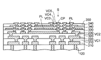
図1は予備的事項に係る配線基板を示す断面図である。図1では、コア基板を有する配線基板のうちのコア基板の上面側が部分的に描かれている。 FIG. 1 is a cross-sectional view showing a wiring board according to a preliminary matter. In FIG. 1, the upper surface side of the core substrate of the wiring substrate having the core substrate is partially depicted.
図1に示すように、予備的事項に係る配線基板では、コア基板100の上面に第1配線層210が形成されている。コア基板100には厚み方向に貫通する貫通導体120が形成されており、第1配線層210はコア基板100の下面側の配線層(不図示)に貫通導体120を介して接続されている。
As shown in FIG. 1, in the wiring board according to the preliminary matter, the
コア基板100の上には第1層間絶縁層310が形成されている。第1層間絶縁層310の上には、第1ビア導体VC1を介して第1配線層210に接続される第2配線層220が形成されている。
A first
また、第1層間絶縁層310の上には、第2層間絶縁層320が形成されている。第2層間絶縁層320の上には、第2ビア導体VC2を介して第2配線層220に接続される第3配線層230が形成されている。
A second
同様に、第2層間絶縁層320の上には、第3層間絶縁層330が形成されている。第3層間絶縁層330の上には、第3ビア導体VC3を介して第3配線層230に接続される金属プレーン層PLが形成されている。
Similarly, a third
さらに同様に、第3層間絶縁層330の上には、第4層間絶縁層340が形成されている。第4層間絶縁層340の上には、第4ビア導体VC4を介して金属プレーン層PLに接続される第4配線層240が形成されている。
Similarly, a fourth
また同様に、第4層間絶縁層340の上には、第5層間絶縁層350が形成されている。第5層間絶縁層350の上には、第5ビア導体VC5を介して第4配線層240に接続される接続パッドCPが形成されている。
Similarly, a fifth
第3、第4配線層230,240は、第1、第2配線層210,220よりも配線ピッチが狭く設定され、微細配線として形成される。微細配線では、特に2本の信号配線が平行に走っている部分でクロストークの影響を受けやすくなり、ノイズによる誤動作が発生しやすい。
The third and
金属プレーン層PLはその下に配置された微細な第3配線層230のパターン間で発生するクロストークを抑制するために形成される。また同様に、金属プレーン層PLはその上に配置された微細な第4配線層240のパターン間で発生するクロストークを抑制するために形成される。金属プレーン層PLはグランドライン又は電源ラインとして形成される。
The metal plane layer PL is formed in order to suppress crosstalk generated between patterns of the fine
微細な第3、第4配線層230,240に近接させて金属プレーン層PLを配置することにより、ノイズとなる信号が金属プレーン層PLに吸収されてクロストークが抑制される。
By arranging the metal plane layer PL close to the fine third and
このように、微細な配線層のパターン間でのクロストークを抑制するために、配線層の上又は下に金属プレーン層PLを挿入する必要がある。金属プレーン層PLは、他の配線層の形成方法と同様な方法によって形成される。このため、配線層の積層数が一層分増えることになるため、製造歩留りの低下の要因になると共に、コスト上昇を招く。 Thus, in order to suppress crosstalk between patterns of fine wiring layers, it is necessary to insert the metal plane layer PL above or below the wiring layers. The metal plane layer PL is formed by a method similar to the method for forming other wiring layers. For this reason, the number of stacked wiring layers is further increased, which causes a reduction in manufacturing yield and an increase in cost.
また、多層配線ではスタックドビア構造を構築するため、金属プレーン層PLの形成時においても、他の配線層と同様にビア受けパッドを配置してスタックドビア構造に対応させる必要がある。 In addition, since a stacked via structure is constructed in the multilayer wiring, it is necessary to arrange a via receiving pad in correspondence with the stacked via structure in the same manner as other wiring layers even when the metal plane layer PL is formed.
図1の例では、Sで示す箇所において、第3配線層230と接続パッドCPとの間に第3ビア導体VC3、第4ビア導体VC4及び第5ビア導体VC5が垂直方向に積層されて、3段のスタックドビア構造が構築されている。
In the example of FIG. 1, the third via conductor VC3, the fourth via conductor VC4, and the fifth via conductor VC5 are stacked in the vertical direction between the
このため、金属プレーン層PLの挿入によってスタックドビア構造の積層数が一つ増えることになるため、接続の信頼性が低下する。 For this reason, since the number of stacked via structures is increased by one by inserting the metal plane layer PL, the reliability of connection is lowered.
微細な多段のスタックドビア構造では、加熱処理によって熱応力が発生すると、スタックドビア構造の最下の部分に応力が集中してビア破断が発生しやすく、電気的な接続の信頼が得られない課題がある。このため、スタックドビア構造の積層数をできるだけ減らすことが好ましい。 In a fine multi-stage stacked via structure, when thermal stress is generated by heat treatment, the stress concentrates on the lowest part of the stacked via structure and the via breaks easily, and there is a problem that reliability of electrical connection cannot be obtained. . For this reason, it is preferable to reduce the number of stacked via structures as much as possible.
以上のように、金属プレーン層PLを他の配線層と同様な方法で形成すると、スタックドビア構造を有する多層配線の積層数が一層分増えるため、製造歩留りの低下及びコスト上昇を招く課題がある。 As described above, when the metal plane layer PL is formed by a method similar to that for other wiring layers, the number of stacked multilayer wirings having a stacked via structure is further increased, and there is a problem in that the manufacturing yield is reduced and the cost is increased.
以下に説明する実施形態の配線基板及びその製造方法では、前述した課題を解決することができる。 In the wiring board and the manufacturing method thereof according to the embodiments described below, the above-described problems can be solved.
(実施形態)
図2〜図12は実施形態の配線基板の製造方法を示す図、図13は実施形態の配線基板を示す図である。以下、配線基板の製造方法を説明しながら、配線基板の構造について説明する。
(Embodiment)
2 to 12 are diagrams showing a method of manufacturing the wiring board according to the embodiment, and FIG. 13 is a diagram showing the wiring board according to the embodiment. Hereinafter, the structure of the wiring board will be described while explaining the manufacturing method of the wiring board.
実施形態の配線基板の製造方法では、まず、図2(a)に示すような構造のコア基板10を用意する。コア基板10には厚み方向に貫通するスルーホールTHが形成されており、スルーホールTHには貫通導体12が形成されている。
In the wiring board manufacturing method of the embodiment, first, a
例えば、スルーホールTHに銅めっきが充填されて貫通導体12が形成される。コア基板10はガラスエポキシ樹脂などの絶縁材料から形成される。
For example, the through
コア基板10の両面側には第1配線層21がそれぞれ形成されている。両面側の第1配線層21は貫通導体12を介して相互接続されている。
First wiring layers 21 are respectively formed on both sides of the
なお、貫通導体12は、コア基板10のスルーホールTHの内壁に形成されたスルーホールめっき層であってもよく、その場合は、スルーホールTHの残りの孔に樹脂体が充填される。
The through
コア基板10のスルーホールTHはドリルやレーザ加工などによって形成される。また、コア基板10に形成される貫通導体12及び第1配線層21は、めっき法及びフォトリソグラフィなどを使用して形成される。
The through hole TH of the
次いで、図2(b)に示すように、コア基板10の両面側に未硬化の樹脂フィルムを貼付し、加熱処理して硬化させることにより、第1層間絶縁層31をそれぞれ形成する。その後に、両面側の第1層間絶縁層31をレーザで加工することにより、両面側の第1配線層21に到達する第1ビアホールVH1をそれぞれ形成する。
Next, as shown in FIG. 2B, uncured resin films are attached to both sides of the
この手法では、第1ビアホールVH1をレーザで形成するため、第1層間絶縁層31は非感光性樹脂から形成される。樹脂材料としては、エポキシ樹脂又はポリイミド樹脂などが使用される。例えば、第1層間絶縁層31の厚みは30μm〜35μm程度であり、第1ビアホールVH1の直径は30μm〜50μm程度である。
In this method, since the first via hole VH1 is formed by a laser, the first
さらに、過マンガン酸法などによって第1ビアホールVH1内をデスミア処理することにより、樹脂スミアを除去してクリーニングする。 Further, the inside of the first via hole VH1 is desmeared by a permanganic acid method or the like to remove the resin smear and clean it.
次いで、図2(c)に示すように、両面側の第1層間絶縁層31の上に、第1ビアホールVH1内の第1ビア導体VC1を介して第1配線層21に接続される第2配線層22をそれぞれ形成する。第2配線層22はセミアディティブ法によって形成される。図3(a)〜(e)を参照して詳しく説明する。図3(a)〜(e)では、図2(b)のコア基板10の上部から上側の領域が部分的に示されている。
Next, as shown in FIG. 2C, the second connected to the
図3(a)に示すように、まず、図2(b)の第1層間絶縁層31上及び第1ビアホールVH1の内面に無電解めっきにより、厚みが1μm程度の銅などからなるシード層22aを形成する。
As shown in FIG. 3A, first, a
次いで、図3(b)に示すように、第2配線層22が配置される部分に開口部14aが設けられためっきレジスト層14を形成する。
Next, as shown in FIG. 3B, a plating resist
続いて、図3(c)に示すように、シード層22aをめっき給電経路に利用する電解めっきにより、めっきレジスト層14の開口部14aに銅などからなる金属めっき層22bを形成する。その後に、図3(d)に示すように、めっきレジスト層14を除去する。
Subsequently, as shown in FIG. 3C, a
さらに、図3(e)に示すように、金属めっき層22bをマスクにしてシード層22aをウェットエッチングにより除去する。これにより、シード層22a及び金属めっき層22bから第2配線層22が形成される。
Further, as shown in FIG. 3E, the
次いで、図4に示すように、上記した図2(b)の工程と同様に、図2(c)の構造体の両面側に、第2配線層22に到達する第2ビアホールVH2が配置された第2層間絶縁層32をそれぞれ形成する。
Next, as shown in FIG. 4, the second via hole VH2 reaching the
さらに、同じく図4に示すように、上記した図2(c)の工程と同様な方法により、下面側の第2層間絶縁層32の上に、第2ビアホールVH2内の第2ビア導体VC2を介して第2配線層22に接続される第3配線層23を形成する。
Further, as shown in FIG. 4, the second via conductor VC2 in the second via hole VH2 is formed on the second
また同時に、上面側の第2層間絶縁層32の上に、第2ビアホールVH2内の第2ビア導体VC2を介して第2配線層22に接続される金属層23aをブランケット状に全面に形成する。
At the same time, a
続いて、図4及び図5に示すように、CMP(Chemical Mechanical Polishing)によって、上面側の金属層23aを第2層間絶縁層32が露出するまで研磨し、さらに、第2層間絶縁層32の表面を研磨して平坦化する。
Subsequently, as shown in FIGS. 4 and 5, the
これにより、図5に示すように、第1、第2配線層21、22の段差の影響で生じた第2層間絶縁層32のグローバル段差が解消され、第2層間絶縁層32の上面は平坦面として形成される。
As a result, as shown in FIG. 5, the global step of the second
そして、図4の第2層間絶縁層32に形成された第2ビア導体VC2がビア電極として残される。これにより、第2ビア導体VC2の上面と第2層間絶縁層32の上面とが同一面となって平坦化される。
Then, the second via conductor VC2 formed in the second
このように、コア基板10の上面側に形成される金属層23aは下地の平坦化のために形成され、研磨によって除去される。
As described above, the
以上により、本実施形態の配線基板のベース基板となる第1の多層配線層5が得られる。前述した図3(a)〜(e)で説明したように、第1の多層配線層5の第2配線層22は、シード層22aをウェットエッチングによって除去する手法のセミアディティブ法によって形成される。
As described above, the first
このため、前述した図3(d)及び(c)の工程で、金属めっき層22bの細りやシード層22aのサイドエッチングによるアンダーカットが生じるため、狭ピッチの配線層を形成することは困難である。
For this reason, in the process of FIG. 3D and FIG. 3C described above, since the
このため、第1の多層配線層5の第2配線層22のライン(幅):スペース(間隔)は、例えば、20μm:20μm以上に設定される。また、第2配線層22の厚みは、例えば、10μm〜30μmに設定される。第1の多層配線層5の第1配線層21においても同じ配線スペックで形成される。
For this reason, the line (width): space (interval) of the
次に、第1の多層配線層5の上に第1、第2配線層21,22よりも配線ピッチの狭い第2の多層配線層を形成する方法について説明する。第1の多層配線層5の配線ピッチはマザーボードなどの実装基板に対応している。第2の多層配線層によって配線ピッチが狭くなるようにピッチ変換することにより、半導体素子の接続に対応できるようにする。
Next, a method for forming a second multilayer wiring layer having a smaller wiring pitch than the first and second wiring layers 21 and 22 on the first
図6に示すように、まず、第1の多層配線層5の第2層間絶縁層32の上に、第2ビア導体VC2に接続される第4配線層24を形成する。第4配線層24は、シード層を異方性ドライエッチングによって除去する手法のセミアディティブ法によって形成される。図7(a)〜(e)を参照して詳しく説明する。図7(a)〜(e)では、図5の上面側の第2層間絶縁層32の上部から上側の領域が部分的に示されている
図7(a)に示すように、まず、図5の第2層間絶縁層32及び第2ビア導体VC2の上にシード層24aを形成する。シード層24aの好適な一例としては、スパッタ法により、厚みが20nm〜50nmのチタン(Ti)層24xを形成した後に、チタン層24xの上に無電解めっきにより厚みが0.5μmの銅(Cu)層24yを形成する。
As shown in FIG. 6, first, a
あるいは、チタン層24xの上にスパッタ法で100nm〜300nmの銅層を形成し、その後に、無電解めっきにより銅層24yを形成してもよい。
Alternatively, a copper layer of 100 nm to 300 nm may be formed on the
次いで、図7(b)に示すように、フォトリソグラフィによって、第4配線層24が配置される領域に開口部16aが設けられためっきレジスト層16をシード層24aの上に形成する。第4配線層24は微細配線として形成されるため、露光装置としてステッパー(ステップ式縮小投影型露光装置)が使用される。
Next, as shown in FIG. 7B, a plating resist
前述したように、第2層間絶縁層32の上面は平坦化されているため、微細パターンを形成する際にフォトリソグラフィの焦点深度が低下するとしても、基板内で精度よく微細なめっきレジスト層16をパターン化することができる。
As described above, since the upper surface of the second
続いて、図7(c)に示すように、シード層24aをめっき給電経路に利用する電解めっきにより、めっきレジスト層16の開口部16aに銅などからなる金属めっき層24bを形成する。その後に、図7(d)に示すように、めっきレジスト層16を除去する。
Subsequently, as shown in FIG. 7C, a
さらに、図7(e)に示すように、金属めっき層24bをマスクにしてシード層24aを異方性ドライエッチングにより除去する。
Further, as shown in FIG. 7E, the
異方性ドライエッチングは、RIE(Reactive Ion Etching)装置、又はICP(Inductively Coupled Plasma)装置などのドライエッチング装置によって行われる。 The anisotropic dry etching is performed by a dry etching apparatus such as an RIE (Reactive Ion Etching) apparatus or an ICP (Inductively Coupled Plasma) apparatus.
異方性ドライエッチングを採用することにより、金属めっき層24bの細りを微小に抑えることができると共に、シード層24aが金属めっき層24bの下端から内側にサイドエッチングすることがない。その結果、シード層24aの幅は金属めっき層24bの幅と同一又はそれより広くなる。
By employing anisotropic dry etching, the
また、第2層間絶縁層32の上面は平坦化されているため、シード層24aをエッチングする際に残渣が発生しにくくなるので、基板内での配線形成の歩留りを向上させることができる。
Further, since the upper surface of the second
なお、枚葉式のスピンエッチング装置などを使用することにより、ウェットエッチングであってもシード層24aをある程度精度よく除去することも可能である。
Note that by using a single-wafer type spin etching apparatus or the like, the
以上により、シード層24a及び金属めっき層24bにより第4配線層24が形成される。
Thus, the
図6に戻って説明すると、第4配線層24は、配線間隔が狭い微細配線として形成された微細配線部Aと、微細配線部Aよりも配線間隔が広く設定された非微細配線部Bとを有して形成される。微細配線部Aの両外側領域に非微細配線部Bが配置される。
Returning to FIG. 6, the
第4配線層24の微細配線部Aでは、ライン(幅):スペース(間隔)Hが、例えば2μm:2μmであり、前述したセミアディティブ方法によって設計スペック内で歩留りよく形成することができる。また、第4配線層24の厚みは、2μm〜3μmの薄膜に設定される。
In the fine wiring portion A of the
これに対して、第4配線層24の非微細配線部Bでは、ライン(幅):スペース(間隔)が、例えば20μm:20μm以上であり、微細配線部Aよりも設計ルールが緩く設定されている。
On the other hand, in the non-fine wiring part B of the
このようにして、第4配線層24の微細配線部Aの配線ピッチを第1の多層配線層5の第1、第2配線層21,22の配線ピッチよりも狭く設定することができる。
In this way, the wiring pitch of the fine wiring portion A of the
以上の方法により、配線間隔が狭い微細配線部Aと、微細配線部Aよりも配線間隔が広い非微細配線部Bとを備えた第4配線層24を含む配線部材を用意する。微細配線部Aを有する第4配線層24は、設計ルールの緩い第1の多層配線層5の上に形成される。
By the above method, a wiring member including the
次いで、図8に示すように、図6の構造体の第2層間絶縁層32及び第4配線層24の上に、感光性樹脂(不図示)を形成し、フォトリソグラフィに基づいて露光・現像を行った後に、加熱処理して硬化させる。感光性樹脂の形成は、液状樹脂を塗布してもよいし、薄膜の樹脂フィルムを貼付してもよい。
Next, as shown in FIG. 8, a photosensitive resin (not shown) is formed on the second
これにより、第4配線層24の接続部上に開口部33aが配置された第3層間絶縁層33が第2層間絶縁層32の上に形成される。
As a result, the third
シリカなどの無機フィラーを含まない感光性樹脂をフォトリソグラフィによってパターニングすることにより、微細な開口部33aを備えた薄膜の第3層間絶縁層33を形成することができる。
By patterning a photosensitive resin not containing an inorganic filler such as silica by photolithography, a thin third
第3層間絶縁層33の好適な一例としては、感光性を有するフェノール系樹脂から形成される永久レジスト層が使用される。以下の他の層間絶縁層を形成する際にも同様な樹脂材料及び形成方法が採用される。
As a suitable example of the third
第3層間絶縁層33の厚みは、第3配線層23の上で2μm〜3μmの薄膜に設定される。また、第3層間絶縁層33に形成される開口部33aの直径は、例えば20μm程度である。
The thickness of the third
次に説明するように、第3層間絶縁層33の上に、第4配線層24の微細配線部Aのパターン間でのクロストークを抑制するために金属プレーン層が形成される。第4配線層24と金属プレーン層とをより近接させる方がクロストークを抑制する効果が高いため、第3層間絶縁層33の厚みは薄膜に設定される。
As will be described next, a metal plane layer is formed on the third
このように、感光性樹脂をフォトリソグラフィでパターニングすることにより、樹脂層をレーザで加工する手法よりも、層間絶縁層の薄膜化及び開口部又はビアホールの狭小化を図ることができる。これによって、微細な多層配線層用の層間絶縁層を形成することができる。 In this manner, by patterning the photosensitive resin by photolithography, it is possible to reduce the thickness of the interlayer insulating layer and narrow the opening or the via hole, as compared with the method of processing the resin layer with a laser. As a result, a fine interlayer insulating layer for a multilayer wiring layer can be formed.
次いで、図9に示すように、第3層間絶縁層33の上に金属プレーン層PLを形成する。金属プレーン層PLはサブトラクティブ法によって形成される。図10(a)〜(d)を参照して詳しく説明する。図10(a)〜(d)では、図8の第2層間絶縁層32の上部から上側の領域が部分的に示されている。
Next, as shown in FIG. 9, a metal plane layer PL is formed on the third
図10(a)に示すように、まず、図8の構造体の上面側の第3層間絶縁層33及びその開口部33aの内面に金属層40aを形成する。金属層40aの一例としては、スパッタ法により厚みが200nmのチタン(Ti)層を形成する。
As shown in FIG. 10A, first, a
次いで、図10(b)に示すように、金属層40aの上にレジスト層18をフォトリソグラフィによってパターニングする。レジスト層18は金属プレーン層PLが配置される領域に残される。金属プレーン層PLは、微細配線を有さず、四角状などの一括パターンで形成されるだけである。このため、露光装置としては、基板に密着させて全面に露光する簡易なコンタクト露光装置が使用される。
Next, as shown in FIG. 10B, the resist
さらに、図10(c)に示すように、レジスト層18をマスクにしてドライエッチングによりレジスト層18から露出する金属層40aを除去する。ドライエッチングとしては、第3層間絶縁層33の開口部33aの側壁に残渣が生じないように等方性ドライエッチングを採用することが好ましい。あるいは、ウェットエッチングを採用してもよい。
Further, as shown in FIG. 10C, the
その後に、レジスト層18が除去される。これより、金属プレーン層PLが配置される領域に無電解めっき用の下地層40がパターン化されて形成される。
Thereafter, the resist
続いて、図10(d)に示すように、無電解めっきにより、下地層40の上に厚みが1μm程度の銅などからなる金属めっき層42を選択的に形成する。
Subsequently, as shown in FIG. 10D, a
これにより、第4配線層24の微細配線部Aに対応する領域の第3層間絶縁層33の上に、下地層40及び金属めっき層42により金属プレーン層PLが形成される。金属プレーン層PLは、グランドプレーン層又は電源プレーン層として形成してもよい。
Thereby, the metal plane layer PL is formed by the
金属プレーン層PLは、第4配線層24の微細配線部Aに対応する領域に一括パターンで形成され、第4配線層24の非微細配線部Bに対応する領域には配置されないようにする。
The metal plane layer PL is formed in a collective pattern in a region corresponding to the fine wiring portion A of the
金属プレーン層PLは、微細な配線層のパターン間で発生するクロストークを抑制するために形成される。第4配線層24の非微細配線部Bは設計ルールが緩く、クロストークが問題にならないため、非微細配線部Bの領域には金属プレーン層PLを配置する必要がないからである。
The metal plane layer PL is formed to suppress crosstalk that occurs between patterns of fine wiring layers. This is because the non-fine wiring portion B of the
金属プレーン層PLは、必ずしも、第4配線層24の微細配線部Aの全体領域に対応するように配置する必要はない。微細配線部Aの周縁側が金属プレーン層PLから多少はみ出していても、十分なクロストーク抑制の効果がある。
The metal plane layer PL is not necessarily arranged so as to correspond to the entire region of the fine wiring portion A of the
これにより、図9及び図10(d)に示すように、金属プレーン層PLの形成工程では、スタックビア構造を構築するためのビア受けパッドの形成が省略される。また、第3層間絶縁層33の開口部33aが露出した状態で、金属プレーン層PLが第3層間絶縁層33の上に形成される。
As a result, as shown in FIGS. 9 and 10D, the formation of the via receiving pad for constructing the stacked via structure is omitted in the formation process of the metal plane layer PL. Further, the metal plane layer PL is formed on the third
前述したように、第4配線層24のクロストーク抑制の効果を高めるため、第3層間絶縁層33は厚みが2μm程度の薄膜で形成される。このため、第3層間絶縁層33はその下の第4配線層24の段差を十分に平坦化できずに凹凸が多少残った状態で形成される。
As described above, the third
しかし、金属プレーン層PLは、第4配線層24の微細配線部Aに対応する領域に一括パターンで形成されるだけで、微細配線を形成する必要はない。従って、第3層間絶縁層33の上面に多少の凹凸が発生していても、金属プレーン層PLを形成する際には問題にならない。
However, the metal plane layer PL is merely formed in a collective pattern in a region corresponding to the fine wiring portion A of the
次いで、図11に示すように、前述した図8の工程と同様な方法により、図9の第3層間絶縁層33及び金属プレーン層PLの上に第4層間絶縁層34をパターン化して形成する。
Next, as shown in FIG. 11, the fourth
第4層間絶縁層34は、第3層間絶縁層33の開口部33aに第3ビアホールVH3が配置され、金属プレーン層PLの上に第4ビアホールVH4が配置されるようにパターン化される。
The fourth
図11の部分拡大断面図を加えて参照すると、第4層間絶縁層34の第3ビアホールVH3の直径は第3層間絶縁層33の開口部33aの直径よりも小さく設定される。そして、第3層間絶縁層33の開口部33aを埋め込む第4層間絶縁層34に第3ビアホールVH3が形成される。第3ビアホールVH3は第3層間絶縁層33の開口部33aの内側に配置される。
Referring to FIG. 11 in addition to the partially enlarged cross-sectional view, the diameter of the third via hole VH3 of the fourth
第4層間絶縁層34においても、上側に形成される第5配線層のクロストーク抑制の効果を高めるために、2μm程度の厚みの薄膜で設定される。
The fourth
金属プレーン層PLは一括パターンで形成されるため、金属プレーン層PLの下地に多少凹凸が発生していても、微細な配線層が形成される場合と比較して、金属プレーン層PLの表面は平坦性が比較的よい状態となっている。 Since the metal plane layer PL is formed in a collective pattern, the surface of the metal plane layer PL is compared with the case where a fine wiring layer is formed even if the metal plane layer PL has some unevenness. The flatness is relatively good.
このため、第4層間絶縁層34が薄膜で金属プレーン層PLの上に形成されるとしても、第4層間絶縁層34の上面の平坦性を確保することができる。また、金属プレーン層PLの厚みは1μm程度と薄いため、その段差を容易に平坦化することができる。
Therefore, even if the fourth
なお、図11の部分拡大断面図の例の他に、第4層間絶縁層34の第3ビアホールVH3の直径を第3層間絶縁層33の開口部33aの直径と同一に設定してもよい。あるいは、図11の部分拡大断面図とは逆に、第4層間絶縁層34の第3ビアホールVH3の直径が第3層間絶縁層33の開口部33aの直径よりも大きく設定され、第3ビアホールVH3が開口部33aの外側に配置されるようにしてもよい。
In addition to the example of the partially enlarged sectional view of FIG. 11, the diameter of the third via hole VH <b> 3 of the fourth
これらの場合は、第3ビアホールVH3及び開口部33aの各側壁が連通して第4配線層24の上にビアホールが形成される。
In these cases, the via hole is formed on the
このようにして、第4層間絶縁層34の上面から第4配線層24に到達するビアホールを形成すればよい。
In this way, a via hole that reaches the
次に説明する図12及び図13では、破線で囲まれた領域が部分拡大断面図で示されている。図12及びその部分拡大断面図に示すように、前述した図7(a)〜(e)の工程と同様な方法により、第3ビアホールVH3内の第3ビア導体VC3を介して第4配線層24に接続される第5配線層25を第4層間絶縁層34の上に形成する。
In FIGS. 12 and 13 to be described next, a region surrounded by a broken line is shown in a partially enlarged sectional view. As shown in FIG. 12 and a partially enlarged cross-sectional view thereof, the fourth wiring layer is formed via the third via conductor VC3 in the third via hole VH3 by the same method as the above-described steps of FIGS. A
また同時に、第4ビアホールVH4内の第4ビア導体VC4を介して金属プレーン層PLに接続される第6配線層26を第4層間絶縁層34の上に形成する。第5配線層25及び第6配線層26は同じ工程で同一層から形成される。
At the same time, a
第5、第6配線層25,26の配線ピッチなどの設計ルールは、前述した図6及び図7で説明した第4配線層24と同様に設定される。第5、第6配線層25,26においても、微細配線部Aとその両外側領域に配置された非微細配線部Bとを有して形成される。
The design rules such as the wiring pitch of the fifth and sixth wiring layers 25 and 26 are set in the same manner as the
第4層間絶縁層34の上面は平坦性が確保されているため、第4層間絶縁層34の上に微細な第5、第6配線層25,26を歩留りよく形成することができる。
Since the upper surface of the fourth
また、図12のSで示される箇所に、第5、第6配線層25,26の形成工程で、スタックドビア構造を構築するためのビア受けパッドVPが形成される。ビア受けパッドVPの下には第3ビアホールVH3内の第3ビア導体VC3が配置されている(部分拡大断面図参照)。 Further, a via receiving pad VP for constructing a stacked via structure is formed at the location indicated by S in FIG. 12 in the step of forming the fifth and sixth wiring layers 25 and 26. A third via conductor VC3 in the third via hole VH3 is disposed under the via receiving pad VP (see a partially enlarged sectional view).
本実施形態で最終的に得られる配線基板では、最上層に複数の半導体素子搭載部が設けられ、上記した第4配線層24又は第5配線層25が複数の半導体素子間を接続する配線層を有して形成される。
In the wiring substrate finally obtained in this embodiment, a plurality of semiconductor element mounting portions are provided in the uppermost layer, and the above-described
その後に、図13及びその部分拡大断面図に示すように、前述した図8の工程と同様な方法により、第5配線層25の上に第5ビアホールVH5が配置された第5層間絶縁層35を形成する。
Thereafter, as shown in FIG. 13 and its partially enlarged sectional view, the fifth
さらに、前述した図7(a)〜(e)の工程と同様な方法により、第5ビアホールVH5内の第5ビア導体VC5を介して第5、第6配線層25,26に接続される接続パッドCPを第5層間絶縁層35の上に形成する(部分拡大断面図参照)。 Further, the connection connected to the fifth and sixth wiring layers 25 and 26 through the fifth via conductor VC5 in the fifth via hole VH5 by the same method as in the steps of FIGS. 7A to 7E described above. A pad CP is formed on the fifth interlayer insulating layer 35 (see a partially enlarged sectional view).
接続パッドCPは第7配線層として形成され、島状に配列されたパッドであってもよいし、引き出し配線の端部に繋がるパッドであってもよい。 The connection pad CP may be a pad formed as a seventh wiring layer and arranged in an island shape, or may be a pad connected to the end of the lead-out wiring.
これにより、第1の多層配線層5の上に第2の多層配線層6が形成される。第2の多層配線層6は、第4配線層24、金属プレーン層PL、第5配線層25、第6配線層26及び接続パッドCPを含んで構築される。
As a result, the second
また、コア基板10の下面側の第2層間絶縁層32の上に、第3配線層23の接続部上に開口部36aが設けられたソルダレジスト層36を形成する。以上により、実施形態の配線基板1が得られる。
Further, a solder resist
図13に示すように、実施形態の配線基板1は、第1の多層配線層5と、その上に配置され、第1の多層配線層5よりも配線ピッチが狭い第2の多層配線層6と備えている。
As shown in FIG. 13, the
第1の多層配線層5では、コア基板10の両面側に第1配線層21がそれぞれ形成されている。両面側の第1配線層21はコア基板10に形成された貫通導体12を介して相互接続されている。
In the first
コア基板の両面側には、第1配線層21に到達する第1ビアホールVH1が配置された第1層間絶縁層31がそれぞれ形成されている。両面側の第1層間絶縁層31の上には第1ビアホールVH1の第1ビア導体VC1を介して第1配線層21に接続される第2配線層22がそれぞれ形成されている。
A first
また、コア基板10の下面側の第1層間絶縁層31の上には、第2配線層22に到達する第2ビアホールVH2が配置された第2層間絶縁層32が形成されている。コア基板10の下面側の第2層間絶縁層32の上には、第2ビアホールVH2内の第2ビア導体VC2を介して第2配線層22に接続される第3配線層23が形成されている。
Further, on the first
さらに、コア基板10の下面側の第2層間絶縁層32の上に、第3配線層23の接続部上に開口部36aが設けられたソルダレジスト層36が形成されている。
Further, on the second
また、コア基板10の上面側の第1層間絶縁層31の上には、第2配線層22に接続される第2ビア導体VC2が配置された第2層間絶縁層32が形成されている。以上により、第1の多層配線層5が構築されている。
A second
次に、第2の多層配線層6について説明する。第1の多層配線層5の第2層間絶縁層32の上には、第2ビア導体VC2に接続された第4配線層24が形成されている。
Next, the second
以下、部分拡大断面図を加えて参照すると、第2層間絶縁層32の上には、第4配線層24の上に開口部33aが配置された第3層間絶縁層33が形成されている。第3層間絶縁層33の上には金属プレーン層PLが形成されている。
Hereinafter, with reference to a partially enlarged sectional view, a third
図14は、図13の金属プレーン層PLが形成されたCで示された部分を水平方向に切断し、上側から金属プレーン層PL及びその下の第4配線層24を透視的にみた模式的な平面図である。図14では、金属プレーン層PL及び第4配線層24以外の要素は省略されている。
FIG. 14 is a schematic diagram in which a portion indicated by C in which the metal plane layer PL of FIG. 13 is formed is cut in the horizontal direction, and the metal plane layer PL and the
図14に示すように、金属プレーン層PLの下方の第4配線層24は、中央部に配置された微細配線部Aと、その両外側領域に配置された非微細配線部Bとを有する。そして、金属プレーン層PLは、第4配線層24の非微細配線部Bを除いた微細配線部Aに対応する領域に配置され、非微細配線部Bに対応する領域には配置されていない。
As shown in FIG. 14, the
金属プレーン層PLによって第4配線層24の微細配線部Aでのクロストークを抑制することができる。第4配線層24の非微細配線部Bではクロストークが問題にならないため、非微細配線部Bには金属プレーン層PLを配置する必要がない。
Crosstalk in the fine wiring portion A of the
図13の部分拡大断面図に戻って説明すると、金属プレーン層PL及び第3層間絶縁層33の上には、第4層間絶縁層34が形成されている。金属プレーン層PLを除く領域には、第4層間絶縁層34の上面から第4配線層24に到達する第3ビアホールVH3が配置されている。
Returning to the partially enlarged sectional view of FIG. 13, a fourth
第3層間絶縁層33には開口部33aが形成されており、その開口部33aを埋め込む第4層間絶縁層34に第3ビアホールVH3が形成されている。第3層間絶縁層33の開口部33aの内側に第3ビアホールVH3が配置されている。第3層間絶縁層33の開口部33aの側壁が第4層間絶縁層34で被覆された状態となっている。
An
また、第4層間絶縁層34には、金属プレーン層PLに到達する第4ビアホールVH4が形成されている。
Further, a fourth via hole VH4 reaching the metal plane layer PL is formed in the fourth
第4層間絶縁層34の上には、第3ビアホールVH3内の第3ビア導体VC3を介して第4配線層24に接続される第5配線層25が形成されている。また、第4層間絶縁層34の上には、第4ビアホールVH4内の第4ビア導体VC4を介して金属プレーン層PLに接続される第6配線層26が形成されている。
On the fourth
第5、第6配線層25、26は同一層から形成され、第4配線層24と同様に、中央部に配置された微細配線部Aと、その両外側領域に配置された非微細配線部Bとを有する。
The fifth and sixth wiring layers 25 and 26 are formed from the same layer. Like the
そして同様に、第5、第6配線層25,26の微細配線部Aに対応する領域に金属プレーン層PLが配置され、第5配線層25の非微細配線部Bに対応する領域には金属プレーン層PLが配置されていない。
Similarly, a metal plane layer PL is disposed in a region corresponding to the fine wiring portion A of the fifth and sixth wiring layers 25 and 26, and a metal corresponding to the non-fine wiring portion B of the
さらに、第4層間絶縁層34の上には、第5、第6配線層25,26に到達する第5ビアホールVH5が配置された第5層間絶縁層35が形成されている。第5層間絶縁層35の上には、第5ビアホールVH5内の第5ビア導体VC5を介して第5,第6配線層25,26に接続される接続パッドCPが第7配線層として形成されている。
Further, a fifth
図13の部分拡大断面図のSで示される箇所に注目すると、第4配線層24の接続部の上に第3ビア導体VC3を介して第5配線層25のビア受けパッドVPが積層されている。さらに、第5配線層25のビア受けパッドVPの上に、第5ビア導体VC5を介して接続パッドCPが積層されている。
When attention is paid to the portion indicated by S in the partial enlarged sectional view of FIG. 13, the via receiving pad VP of the
このようにして、第5配線層25のビア受けパッドVPの上下の第3ビア導体VC3及び第5ビア導体CV5よって2段のスタックドビア構造が構築されている。
In this way, a two-stage stacked via structure is constructed by the third via conductor VC3 and the fifth via conductor CV5 above and below the via receiving pad VP of the
前述したように、金属プレーン層PLは、第4配線層24及び第5、第6配線層25,26の各微細配線部Aに対応する領域のみに配置される。これにより、金属プレーン層PLを形成する工程では、スタックドビア構造を構築するためのビア受けパッドを省略している。
As described above, the metal plane layer PL is disposed only in regions corresponding to the fine wiring portions A of the
その代わりに、金属プレーン層PLの上下に配置された第4層間絶縁層34及び第3層間絶縁層33を貫通するように第3ビアホールVH3を形成し、金属プレーン層PLの上に形成された第4層間絶縁層34の上に第5配線層25のビア受けパッドVPを形成している。
Instead, the third via hole VH3 is formed so as to penetrate the fourth
このようにすることにより、第4配線層24と第5、第6配線層25,26との間に金属プレーン層PLを挿入しても、スタックドビア構造の積層数が増加しない。このため、金属プレーン層PLを追加で形成しても、スタックビア構造の電気的な接続の信頼性を確保することができる。
In this way, even if the metal plane layer PL is inserted between the
また、金属プレーン層PLを形成する工程では、スタックドビア構造用のビア受けパッドなどの微細配線を形成することなく、一括パターンを形成するだけなので、サブトラクティブ法などの簡易な方法を採用することができる。 Further, in the process of forming the metal plane layer PL, a simple pattern such as a subtractive method can be adopted because only a collective pattern is formed without forming a fine wiring such as a via receiving pad for a stacked via structure. it can.
従って、微細な第4配線層24及び第5、第6配線層25,26を形成する工程と違って、技術的な難易度が高いセミアディティブ法を使用する必要がないため、金属プレーン層PLを追加で形成するとしても、製造歩留りが低下するおそれがない。
Therefore, unlike the process of forming the fine
また、金属プレーン層PLをサブトラクティブ法などの簡易な方法で形成できるため、微細配線形成用のセミアディティブ法を使用する場合より、製造コストの低減を図ることができる。 Further, since the metal plane layer PL can be formed by a simple method such as a subtractive method, the manufacturing cost can be reduced as compared with the case of using the semi-additive method for forming fine wiring.
図13の部分拡大断面図に示すように、第4配線層24と金属プレーン層PLとの間の第3層間絶縁層33は、厚みT1が2μm程度の薄膜で形成されている。また同様に、金属プレーン層PLと第5、第6配線層25,26との間の第4層間絶縁層34においても、厚みT2が2μm程度の薄膜で形成されている。
As shown in the partially enlarged sectional view of FIG. 13, the third
これにより、第4配線層24及び第5、第6配線層25、26の各微細配線部Aは金属プレーン層PLに十分に近接して形成されるため、十分なクロストーク抑制の効果が得られる。
As a result, the fine wiring portions A of the
また、金属プレーン層PLでは、スタックドビア構造用のビア受けパッドの形成を省略している、このため、第4配線層24と第5配線層25とは、金属プレーン層PLの上下に配置された第3、第4層間絶縁層33,34を貫通する第3ビアホールVH3内の第3ビア導体VC3を介して接続される。
Further, in the metal plane layer PL, the formation of the via receiving pad for the stacked via structure is omitted. Therefore, the
また、金属プレーン層PLは、その上の第4層間絶縁層34に形成された第4ビアホールVH4内の第4ビア導体VC4を介して上側の第6配線層26に接続されている。
The metal plane layer PL is connected to the upper
このように、金属プレーン層PLと第6配線層26とを接続する第4ビアホールVH4の深さ(厚み:T1)は、第4配線層24と第5配線層25とを接続する第3ビアホールVH3の深さ(厚み:T3)よりも浅くなる。
Thus, the depth (thickness: T1) of the fourth via hole VH4 connecting the metal plane layer PL and the
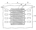
図15には、図13の配線基板1を使用する半導体装置2が示されている。図15に示すように、図13の配線基板1には複数の半導体素子搭載部が設けられており、上面側の接続パッドCPに複数の半導体素子50の接続端子52がはんだを介してフリップチップ接続される。
FIG. 15 shows a
配線基板1の第4配線層24又は第5配線層25が複数の半導体素子50間を接続する配線を有して形成される。さらに、複数の半導体素子50と配線基板1との間にアンダーフィル樹脂54が充填される。
The
複数の半導体素子50としては、例えば、CPUなどの複数のロジックチップを搭載してもよいし、あるいは、ロジックチップとメモリチップとを搭載してもよい。
As the plurality of
さらに、配線基板1の下面側の第3配線層23にはんだボールを搭載するなどして外部接続端子Tを形成する。
Further, the external connection terminals T are formed by mounting solder balls on the
以上により、実施形態の半導体装置2が得られる。実施形態の半導体装置2では、半導体素子50が微細配線を有する第2の多層配線層6に接続され、その下の第1の多層配線層5によって配線ピッチが広くなるようにピッチ変換される。
As described above, the
そして、半導体装置2の外部接続端子Tがマザーボードなどの実装基板の接続部に接続される。第2の多層配線層6は狭ピッチで形成できるため、高性能な半導体素子50の実装基板として使用できる。また、金属プレーン層PLによってクロストークが抑制されるため、信頼性を向上させることができる。
And the external connection terminal T of the
なお、図15の半導体装置2の配線基板1では、1層の金属プレーン層PLが形成されているが、金属プレーン層PLの層数は、微細配線の積層数に応じて任意の層数で形成することができる。
In the
図16の半導体装置2aの配線基板1aでは、2層の金属プレーン層PLが形成された例が示されている。第1配線層61の上に第1層間絶縁層71を介して第1金属プレーン層PL1が形成されている。第1金属プレーン層PL1の上に第2層間絶縁層72を介して第2配線層62が形成されている。
In the
さらに、第2配線層62の上に第3層間絶縁層73を介して第2金属プレーン層PL2が形成されている。第2金属プレーン層PL2の上に第4層間絶縁層74を介して第3配線層63が形成されている。
Further, a second metal plane layer PL2 is formed on the
第3配線層63の上には第5層間絶縁層75を介して接続パッドCPが形成されている。接続パッドCPに半導体素子50の接続端子52がフリップチップ接続されている。さらに、半導体素子50と配線基板1aとの間にアンダーフィル樹脂54が充填されている。
A connection pad CP is formed on the
このように、第1配線層61と第2配線層62との間に第1金属プレーン層PL1が形成されている。また、第2配線層62と第3配線層63との間に第2金属プレーン層PL2が形成されている。
As described above, the first metal plane layer PL <b> 1 is formed between the
第1配線層61、第1金属プレーン層PL1及び第2配線層62を接続する第1ビアホールVHA及び第2ビアホールVHBの接続形態は、前述した図13の部分拡大断面図と同一である。
The connection form of the first via hole VHA and the second via hole VHB connecting the
また、第2配線層62、第2金属プレーン層PL2及び第3配線層63を接続する第3ビアホールVHC及び第4ビアホールVHDの接続形態についても、前述した図13の部分拡大図と同一である。
The connection form of the third via hole VHC and the fourth via hole VHD connecting the
図16では、図13の第3層間絶縁層33の開口部33aに対応する第1層間絶縁層71及び第3層間絶縁層73の各開口部は省略されて描かれている。
In FIG. 16, the openings of the first
図16の半導体装置2aの配線基板1aでは、図13の配線基板1と同様に、第1配線層61、第2配線層62及び第3配線層63が微細配線部Aと非微細配線部B(不図示)とをそれぞれ有している。そして、各微細配線部Aに対応する領域のみに第1、第2金属プレーン層PL1,PL2が配置されている。
In the
また同様に、第1、第2金属プレーン層PL1,PL2を形成する際に、スタックドビア構造用のビア受けパッドを省略している。 Similarly, the via receiving pads for the stacked via structure are omitted when the first and second metal plane layers PL1 and PL2 are formed.
このため、複数の金属プレーン層を挿入する場合であっても、スタックドビア構造の積層数が増加しないため、接続の信頼性を確保することができる。また、前述したように、金属プレーン層の形成工程では、微細配線を形成する必要がなくなるため、金属プレーン層は簡易な方法で歩留りよく形成される。 Therefore, even when a plurality of metal plane layers are inserted, the number of stacked via structures is not increased, so that connection reliability can be ensured. Further, as described above, in the process of forming the metal plane layer, it is not necessary to form fine wiring, so that the metal plane layer is formed with a simple method and with a high yield.
このように、金属プレーン層の形成は歩留り低下の要因にはならないため、複数の金属プレーン層を追加で形成しても、歩留りの低下が回避される。 Thus, since the formation of the metal plane layer does not cause a decrease in yield, even if a plurality of metal plane layers are additionally formed, a decrease in yield is avoided.
1,1a…配線基板、2,2a…半導体装置、5…第1の多層配線層、6…第2の多層配線層、10…コア基板、12…貫通導体、14,16…めっきレジスト層、14a,16a,33a,36a…開口部、18…レジスト層、21,61…第1配線層、22,62…第2配線層,22a,24a…シード層、22b,24b…金属めっき層、23,63…第3配線層、23a,40a…金属層、24…第4配線層、24x…チタン層、24y…銅層、25…第5配線層、31,71…第1層間絶縁層,32,72…第2層間絶縁層、33,73…第3層間絶縁層、34,74…第4層間絶縁層、35,75…第5層間絶縁層、36…ソルダレジスト層、40…下地層、42…金属めっき層、50…半導体素子、52…接続端子、54…アンダーフィル樹脂、A…微細配線部、B…非微細配線部、CP…接続パッド、PL,PL1,PL2…金属プレーン層、TH…スルーホール、T…外部接続端子、VC1,VC2,VC3,VC4,VC5…ビア導体、VH1,VH2,VH3,VH4,VH5,VHA,VHB,VHC,VHD…ビアホール、VP…ビア受けパッド。
DESCRIPTION OF
Claims (11)
前記第1配線層の上に形成された第1絶縁層と、
前記配線間隔が狭い配線部上の第1絶縁層の上に形成された金属プレーン層と、
前記第1絶縁層及び前記金属プレーン層の上に形成された第2絶縁層と、
前記第2絶縁層の上面から前記第1配線層に到達する第1ビアホールと、
前記第1ビアホールに形成された第1ビア導体と、
前記第2絶縁層に形成され、前記金属プレーン層に到達する第2ビアホールと、
前記第2ビアホールに形成された第2ビア導体と、
前記第2絶縁層の上に形成され、前記第1ビア導体を介して前記第1配線層に接続される第2配線層と、
前記第2絶縁層の上に形成され、前記第2ビア導体を介して前記金属プレーン層に接続された第3配線層と、
前記第2配線層の上に形成された第3絶縁層と、
前記第3絶縁層に形成され、前記第2配線層に到達する第3ビアホールと、
前記第3ビアホールに形成された第3ビア導体と、
前記第3絶縁層の上に形成され、前記第3ビア導体を介して前記第2配線層に接続された第4配線層とを有し、
前記第2配線層はビア受けパッドであり、前記第2配線層の上下に配置された前記第1ビア導体と前記第3ビア導体とによってスタックドビア構造が構築されていることを特徴とする配線基板。 A first wiring layer comprising a wiring portion having a narrow wiring interval and a wiring portion having a wiring interval wider than the wiring portion;
A first insulating layer formed on the first wiring layer;
A metal plane layer formed on the first insulating layer on the wiring portion having a narrow wiring interval;
A second insulating layer formed on the first insulating layer and the metal plane layer;
A first via hole reaching the first wiring layer from an upper surface of the second insulating layer;
A first via conductor formed in the first via hole;
A second via hole formed in the second insulating layer and reaching the metal plane layer;
A second via conductor formed in the second via hole;
A second wiring layer formed on the second insulating layer and connected to the first wiring layer via the first via conductor;
A third wiring layer formed on the second insulating layer and connected to the metal plane layer through the second via conductor;
A third insulating layer formed on the second wiring layer;
A third via hole formed in the third insulating layer and reaching the second wiring layer;
A third via conductor formed in the third via hole;
A fourth wiring layer formed on the third insulating layer and connected to the second wiring layer via the third via conductor;
The wiring board, wherein the second wiring layer is a via receiving pad, and a stacked via structure is constructed by the first via conductor and the third via conductor arranged above and below the second wiring layer. .
第1の多層配線層と、
前記第1の多層配線層の上に形成され、前記第1の多層配線層よりも配線ピッチが狭い第2の多層配線層とを備え、
前記第2の多層配線層が、前記第1配線層、前記金属プレーン層、前記第2配線層及び前記第3配線層を含むことを特徴とする請求項1又は2に記載の配線基板。 The wiring board is
A first multilayer wiring layer;
A second multilayer wiring layer formed on the first multilayer wiring layer and having a wiring pitch narrower than the first multilayer wiring layer;
The wiring board according to claim 1, wherein the second multilayer wiring layer includes the first wiring layer, the metal plane layer, the second wiring layer, and the third wiring layer.
前記第1配線層の接続部上に開口部が配置された第1絶縁層を形成する工程と、
前記配線間隔が狭い配線部上の第1絶縁層の上に金属プレーン層を形成する工程と、
前記第1絶縁層及び前記金属プレーン層の上に、前記第1絶縁層の開口部に第1ビアホールが配置され、前記金属プレーン層の上に第2ビアホールが配置された第2絶縁層を形成する工程と、
前記第2絶縁層の上に、前記第1ビアホール内の第1ビア導体を介して前記第1配線層に接続される第2配線層と、前記第2ビアホール内の第2ビア導体を介して前記金属プレーン層に接続される第3配線層とを形成する工程と
を有することを特徴とする配線基板の製造方法。 Preparing a wiring member including a first wiring layer provided with a wiring portion having a narrow wiring interval and a wiring portion having a wiring interval wider than the wiring portion;
Forming a first insulating layer having an opening disposed on a connection portion of the first wiring layer;
Forming a metal plane layer on the first insulating layer on the wiring portion having a narrow wiring interval;
A second insulating layer is formed on the first insulating layer and the metal plane layer, wherein a first via hole is disposed in an opening of the first insulating layer, and a second via hole is disposed on the metal plane layer. And a process of
A second wiring layer connected to the first wiring layer via a first via conductor in the first via hole and a second via conductor in the second via hole on the second insulating layer. Forming a third wiring layer connected to the metal plane layer. A method for manufacturing a wiring board, comprising:
前記第1ビアホールは、前記第1絶縁層の開口部の内側に配置されることを特徴とする請求項6に記載の配線基板の製造方法。 In the step of forming the second insulating layer,
The method of manufacturing a wiring board according to claim 6 , wherein the first via hole is disposed inside an opening of the first insulating layer.
前記第2配線層及び第3配線層の上に第3絶縁層を形成する工程と、
前記第2配線層に到達する第3ビアホールを前記第3絶縁層に形成する工程と、
前記第3絶縁層の上に、前記第3ビアホール内の第3ビア導体を介して前記第2配線層に接続される第4配線層を形成する工程と
を有し、
前記第2配線層はビア受けパッドであり、前記第2配線層の上下に配置された前記第1ビア導体と前記第3ビア導体とによってスタックドビア構造が構築されることを特徴とする請求項6又は7に記載の配線基板の製造方法。 After the step of forming the second wiring layer and the third wiring layer,
Forming a third insulating layer on the second wiring layer and the third wiring layer;
Forming a third via hole in the third insulating layer reaching the second wiring layer;
Forming a fourth wiring layer connected to the second wiring layer on the third insulating layer via a third via conductor in the third via hole;
7. The stacked wiring structure according to claim 6, wherein the second wiring layer is a via receiving pad, and a stacked via structure is constructed by the first via conductor and the third via conductor arranged above and below the second wiring layer. Or the manufacturing method of the wiring board of Claim 7.
前記第1配線層、前記金属プレーン層、前記第2配線層及び前記第3配線層を含んで第2の多層配線層が構築され、
前記第2の多層配線層は、前記第1の多層配線層よりも配線ピッチが狭いことを特徴とする請求項6又は7に記載の配線基板の製造方法。 In the step of preparing the wiring member, the wiring member includes a first multilayer wiring layer under the first wiring layer,
A second multilayer wiring layer is constructed including the first wiring layer, the metal plane layer, the second wiring layer, and the third wiring layer;
The method for manufacturing a wiring board according to claim 6, wherein the second multilayer wiring layer has a wiring pitch narrower than that of the first multilayer wiring layer.
前記金属プレーン層を形成する工程は、
前記第1絶縁層の上に金属層を形成する工程と、
前記金属層をパターニングして下地層を形成する工程と、
無電解めっきにより前記下地層の上に金属めっき層を形成する工程とを含むことを特徴とする請求項6乃至9のいずれか一項に記載の配線基板の製造方法。 In the step of forming the first wiring layer and the step of forming the second wiring layer and the third wiring layer, a semi-additive method for removing the seed layer by anisotropic dry etching is used.
The step of forming the metal plane layer includes
Forming a metal layer on the first insulating layer;
Forming a base layer by patterning the metal layer;
The method for manufacturing a wiring board according to claim 6 , further comprising: forming a metal plating layer on the base layer by electroless plating.
Priority Applications (3)
| Application Number | Priority Date | Filing Date | Title |
|---|---|---|---|
| JP2014122705A JP6332680B2 (en) | 2014-06-13 | 2014-06-13 | Wiring board and manufacturing method thereof |
| US14/734,395 US9412687B2 (en) | 2014-06-13 | 2015-06-09 | Wiring substrate and method of manufacturing the same |
| US15/170,313 US9646926B2 (en) | 2014-06-13 | 2016-06-01 | Wiring substrate and method of manufacturing the same |
Applications Claiming Priority (1)
| Application Number | Priority Date | Filing Date | Title |
|---|---|---|---|
| JP2014122705A JP6332680B2 (en) | 2014-06-13 | 2014-06-13 | Wiring board and manufacturing method thereof |
Publications (3)
| Publication Number | Publication Date |
|---|---|
| JP2016004833A JP2016004833A (en) | 2016-01-12 |
| JP2016004833A5 JP2016004833A5 (en) | 2017-02-09 |
| JP6332680B2 true JP6332680B2 (en) | 2018-05-30 |
Family
ID=54836784
Family Applications (1)
| Application Number | Title | Priority Date | Filing Date |
|---|---|---|---|
| JP2014122705A Active JP6332680B2 (en) | 2014-06-13 | 2014-06-13 | Wiring board and manufacturing method thereof |
Country Status (2)
| Country | Link |
|---|---|
| US (2) | US9412687B2 (en) |
| JP (1) | JP6332680B2 (en) |
Families Citing this family (13)
| Publication number | Priority date | Publication date | Assignee | Title |
|---|---|---|---|---|
| JP6341714B2 (en) | 2014-03-25 | 2018-06-13 | 新光電気工業株式会社 | Wiring board and manufacturing method thereof |
| JP6527420B2 (en) * | 2015-07-31 | 2019-06-05 | ルネサスエレクトロニクス株式会社 | Semiconductor device |
| EP3430646B1 (en) * | 2016-03-16 | 2021-11-10 | INTEL Corporation | Stairstep interposers with integrated shielding for electronics packages |
| JP2019062092A (en) * | 2017-09-27 | 2019-04-18 | イビデン株式会社 | Printed wiring board |
| CN110504275B (en) * | 2018-05-17 | 2021-11-12 | 京东方科技集团股份有限公司 | Array substrate, manufacturing method thereof, display panel and display device |
| US10888001B2 (en) | 2018-06-08 | 2021-01-05 | Unimicron Technology Corp. | Circuit carrier board structure and manufacturing method thereof |
| US11032917B2 (en) | 2018-06-08 | 2021-06-08 | Unimicron Technology Corp. | Circuit carrier board and manufacturing method thereof |
| TWI734945B (en) * | 2018-12-12 | 2021-08-01 | 欣興電子股份有限公司 | Composite substrate structure and manufacturing method thereof |
| US20220223456A1 (en) * | 2019-05-20 | 2022-07-14 | Mitsui Mining & Smelting Co., Ltd. | Metal foil with carrier and use method and manufacturing method therefor |
| KR20220001568A (en) * | 2020-06-30 | 2022-01-06 | 삼성전기주식회사 | Printed circuit board |
| US20220051989A1 (en) * | 2020-08-12 | 2022-02-17 | Advanced Micro Devices, Inc. | Mixed density interconnect architectures using hybrid fan-out |
| WO2022264378A1 (en) * | 2021-06-17 | 2022-12-22 | 昭和電工マテリアルズ株式会社 | Method for manufacturing wiring board, and laminated board |
| US20230073823A1 (en) * | 2021-09-09 | 2023-03-09 | Qualcomm Incorporated | Package comprising a substrate with high-density interconnects |
Family Cites Families (17)
| Publication number | Priority date | Publication date | Assignee | Title |
|---|---|---|---|---|
| JP2998237B2 (en) * | 1991-03-07 | 2000-01-11 | ソニー株式会社 | Processing method of blind hole |
| US5510758A (en) * | 1993-04-07 | 1996-04-23 | Matsushita Electric Industrial Co., Ltd. | Multilayer microstrip wiring board with a semiconductor device mounted thereon via bumps |
| US5635761A (en) * | 1994-12-14 | 1997-06-03 | International Business Machines, Inc. | Internal resistor termination in multi-chip module environments |
| JP3199592B2 (en) * | 1995-01-27 | 2001-08-20 | 株式会社日立製作所 | Multilayer printed circuit board |
| JP2001203470A (en) * | 2000-01-21 | 2001-07-27 | Toshiba Corp | Wiring board, semiconductor package and semiconductor device |
| JP3582460B2 (en) * | 2000-06-20 | 2004-10-27 | 株式会社村田製作所 | High frequency module |
| JP2003023252A (en) | 2001-07-10 | 2003-01-24 | Ibiden Co Ltd | Multilayered printed wiring board |
| JP5191074B2 (en) | 2001-07-10 | 2013-04-24 | イビデン株式会社 | Multilayer printed wiring board |
| JP2002329976A (en) * | 2001-04-26 | 2002-11-15 | Kyocera Corp | Multilayer wiring board |
| JP4195883B2 (en) * | 2004-02-04 | 2008-12-17 | インターナショナル・ビジネス・マシーンズ・コーポレーション | Multilayer module |
| JP2007165642A (en) * | 2005-12-14 | 2007-06-28 | Mitsubishi Electric Corp | Component mounting substrate |
| US7820233B2 (en) * | 2006-09-27 | 2010-10-26 | Unimicron Technology Corp. | Method for fabricating a flip chip substrate structure |
| JP4978269B2 (en) * | 2007-03-27 | 2012-07-18 | 日本電気株式会社 | Multilayer wiring board |
| JP5649490B2 (en) * | 2011-03-16 | 2015-01-07 | 新光電気工業株式会社 | Wiring board and manufacturing method thereof |
| KR102134933B1 (en) * | 2012-08-31 | 2020-07-16 | 소니 주식회사 | Wiring substrate and wiring substrate fabrication method |
| JP6013960B2 (en) * | 2013-03-28 | 2016-10-25 | 京セラ株式会社 | Wiring board |
| JP2014229698A (en) * | 2013-05-21 | 2014-12-08 | イビデン株式会社 | Wiring board and manufacturing method therefor |
-
2014
- 2014-06-13 JP JP2014122705A patent/JP6332680B2/en active Active
-
2015
- 2015-06-09 US US14/734,395 patent/US9412687B2/en active Active
-
2016
- 2016-06-01 US US15/170,313 patent/US9646926B2/en active Active
Also Published As
| Publication number | Publication date |
|---|---|
| US20150364405A1 (en) | 2015-12-17 |
| US9412687B2 (en) | 2016-08-09 |
| US9646926B2 (en) | 2017-05-09 |
| US20160276259A1 (en) | 2016-09-22 |
| JP2016004833A (en) | 2016-01-12 |
Similar Documents
| Publication | Publication Date | Title |
|---|---|---|
| JP6332680B2 (en) | Wiring board and manufacturing method thereof | |
| JP6539992B2 (en) | Printed circuit board, semiconductor device, method of manufacturing wired circuit board, method of manufacturing semiconductor device | |
| JP6358431B2 (en) | Electronic component device and manufacturing method thereof | |
| TWI670803B (en) | Interposer, semiconductor device, interposer manufacturing method, and semiconductor device manufacturing method | |
| JP2014154800A (en) | Wiring board and manufacturing method thereof | |
| JP6418757B2 (en) | WIRING BOARD, MANUFACTURING METHOD THEREOF, AND SEMICONDUCTOR DEVICE | |
| JP5547615B2 (en) | WIRING BOARD, SEMICONDUCTOR DEVICE, AND WIRING BOARD MANUFACTURING METHOD | |
| TWI543676B (en) | Printed circuit board and method of manufacturing the same | |
| JP6566726B2 (en) | WIRING BOARD AND WIRING BOARD MANUFACTURING METHOD | |
| US9392684B2 (en) | Wiring substrate and method for manufacturing wiring substrate | |
| JP6316609B2 (en) | WIRING BOARD, SEMICONDUCTOR DEVICE, WIRING BOARD MANUFACTURING METHOD, AND SEMICONDUCTOR DEVICE MANUFACTURING METHOD | |
| US9324580B2 (en) | Process for fabricating a circuit substrate | |
| JP5509508B2 (en) | Electronic component and method for manufacturing electronic component | |
| JP6660850B2 (en) | Electronic component built-in substrate, method of manufacturing the same, and electronic component device | |
| JP2015165533A5 (en) | ||
| JP4841806B2 (en) | Capacitor device, semiconductor device including the same, and method of manufacturing capacitor device | |
| JP6619294B2 (en) | WIRING BOARD, MANUFACTURING METHOD THEREOF, AND ELECTRONIC COMPONENT DEVICE | |
| KR20110112974A (en) | Package substrate and fabricating method of the same | |
| JP2009135147A (en) | Connection structure of wiring board and electronic element, and electronic device | |
| JP4759981B2 (en) | Manufacturing method of electronic component built-in module | |
| JP2016219730A (en) | Electronic component built-in board and manufacturing method therefor and electronic device | |
| KR102521788B1 (en) | Manufacturing method of multi-layered printed circuit board of deep cavity structure | |
| JP5363377B2 (en) | Wiring board and manufacturing method thereof | |
| JP2006049762A (en) | Part built-in substrate and manufacturing method thereof | |
| JP5825111B2 (en) | Silicon interposer and semiconductor device using the same |
Legal Events
| Date | Code | Title | Description |
|---|---|---|---|
| A521 | Request for written amendment filed |
Free format text: JAPANESE INTERMEDIATE CODE: A523 Effective date: 20161221 |
|
| A621 | Written request for application examination |
Free format text: JAPANESE INTERMEDIATE CODE: A621 Effective date: 20161221 |
|
| A977 | Report on retrieval |
Free format text: JAPANESE INTERMEDIATE CODE: A971007 Effective date: 20170927 |
|
| A131 | Notification of reasons for refusal |
Free format text: JAPANESE INTERMEDIATE CODE: A131 Effective date: 20171121 |
|
| A521 | Request for written amendment filed |
Free format text: JAPANESE INTERMEDIATE CODE: A523 Effective date: 20180112 |
|
| TRDD | Decision of grant or rejection written | ||
| A01 | Written decision to grant a patent or to grant a registration (utility model) |
Free format text: JAPANESE INTERMEDIATE CODE: A01 Effective date: 20180403 |
|
| A61 | First payment of annual fees (during grant procedure) |
Free format text: JAPANESE INTERMEDIATE CODE: A61 Effective date: 20180418 |
|
| R150 | Certificate of patent or registration of utility model |
Ref document number: 6332680 Country of ref document: JP Free format text: JAPANESE INTERMEDIATE CODE: R150 |