JP6307829B2 - Circuit device and electronic device - Google Patents
Circuit device and electronic device Download PDFInfo
- Publication number
- JP6307829B2 JP6307829B2 JP2013208887A JP2013208887A JP6307829B2 JP 6307829 B2 JP6307829 B2 JP 6307829B2 JP 2013208887 A JP2013208887 A JP 2013208887A JP 2013208887 A JP2013208887 A JP 2013208887A JP 6307829 B2 JP6307829 B2 JP 6307829B2
- Authority
- JP
- Japan
- Prior art keywords
- delay time
- side transistor
- pulse signal
- drive pulse
- delay
- Prior art date
- Legal status (The legal status is an assumption and is not a legal conclusion. Google has not performed a legal analysis and makes no representation as to the accuracy of the status listed.)
- Active
Links
Images


Classifications
-
- H—ELECTRICITY
- H02—GENERATION; CONVERSION OR DISTRIBUTION OF ELECTRIC POWER
- H02M—APPARATUS FOR CONVERSION BETWEEN AC AND AC, BETWEEN AC AND DC, OR BETWEEN DC AND DC, AND FOR USE WITH MAINS OR SIMILAR POWER SUPPLY SYSTEMS; CONVERSION OF DC OR AC INPUT POWER INTO SURGE OUTPUT POWER; CONTROL OR REGULATION THEREOF
- H02M7/00—Conversion of ac power input into dc power output; Conversion of dc power input into ac power output
- H02M7/42—Conversion of dc power input into ac power output without possibility of reversal
- H02M7/44—Conversion of dc power input into ac power output without possibility of reversal by static converters
- H02M7/48—Conversion of dc power input into ac power output without possibility of reversal by static converters using discharge tubes with control electrode or semiconductor devices with control electrode
- H02M7/53—Conversion of dc power input into ac power output without possibility of reversal by static converters using discharge tubes with control electrode or semiconductor devices with control electrode using devices of a triode or transistor type requiring continuous application of a control signal
- H02M7/537—Conversion of dc power input into ac power output without possibility of reversal by static converters using discharge tubes with control electrode or semiconductor devices with control electrode using devices of a triode or transistor type requiring continuous application of a control signal using semiconductor devices only, e.g. single switched pulse inverters
- H02M7/5387—Conversion of dc power input into ac power output without possibility of reversal by static converters using discharge tubes with control electrode or semiconductor devices with control electrode using devices of a triode or transistor type requiring continuous application of a control signal using semiconductor devices only, e.g. single switched pulse inverters in a bridge configuration
-
- H—ELECTRICITY
- H02—GENERATION; CONVERSION OR DISTRIBUTION OF ELECTRIC POWER
- H02M—APPARATUS FOR CONVERSION BETWEEN AC AND AC, BETWEEN AC AND DC, OR BETWEEN DC AND DC, AND FOR USE WITH MAINS OR SIMILAR POWER SUPPLY SYSTEMS; CONVERSION OF DC OR AC INPUT POWER INTO SURGE OUTPUT POWER; CONTROL OR REGULATION THEREOF
- H02M1/00—Details of apparatus for conversion
- H02M1/38—Means for preventing simultaneous conduction of switches
-
- H—ELECTRICITY
- H02—GENERATION; CONVERSION OR DISTRIBUTION OF ELECTRIC POWER
- H02P—CONTROL OR REGULATION OF ELECTRIC MOTORS, ELECTRIC GENERATORS OR DYNAMO-ELECTRIC CONVERTERS; CONTROLLING TRANSFORMERS, REACTORS OR CHOKE COILS
- H02P7/00—Arrangements for regulating or controlling the speed or torque of electric DC motors
- H02P7/03—Arrangements for regulating or controlling the speed or torque of electric DC motors for controlling the direction of rotation of DC motors
- H02P7/04—Arrangements for regulating or controlling the speed or torque of electric DC motors for controlling the direction of rotation of DC motors by means of a H-bridge circuit
-
- H—ELECTRICITY
- H02—GENERATION; CONVERSION OR DISTRIBUTION OF ELECTRIC POWER
- H02P—CONTROL OR REGULATION OF ELECTRIC MOTORS, ELECTRIC GENERATORS OR DYNAMO-ELECTRIC CONVERTERS; CONTROLLING TRANSFORMERS, REACTORS OR CHOKE COILS
- H02P7/00—Arrangements for regulating or controlling the speed or torque of electric DC motors
- H02P7/06—Arrangements for regulating or controlling the speed or torque of electric DC motors for regulating or controlling an individual dc dynamo-electric motor by varying field or armature current
- H02P7/18—Arrangements for regulating or controlling the speed or torque of electric DC motors for regulating or controlling an individual dc dynamo-electric motor by varying field or armature current by master control with auxiliary power
- H02P7/24—Arrangements for regulating or controlling the speed or torque of electric DC motors for regulating or controlling an individual dc dynamo-electric motor by varying field or armature current by master control with auxiliary power using discharge tubes or semiconductor devices
- H02P7/28—Arrangements for regulating or controlling the speed or torque of electric DC motors for regulating or controlling an individual dc dynamo-electric motor by varying field or armature current by master control with auxiliary power using discharge tubes or semiconductor devices using semiconductor devices
- H02P7/285—Arrangements for regulating or controlling the speed or torque of electric DC motors for regulating or controlling an individual dc dynamo-electric motor by varying field or armature current by master control with auxiliary power using discharge tubes or semiconductor devices using semiconductor devices controlling armature supply only
- H02P7/29—Arrangements for regulating or controlling the speed or torque of electric DC motors for regulating or controlling an individual dc dynamo-electric motor by varying field or armature current by master control with auxiliary power using discharge tubes or semiconductor devices using semiconductor devices controlling armature supply only using pulse modulation
Landscapes
- Engineering & Computer Science (AREA)
- Power Engineering (AREA)
- Electronic Switches (AREA)
Description
本発明は、回路装置及び電子機器等に関する。 The present invention relates to a circuit device, an electronic device, and the like.
トランジスターのオン・オフにより外部回路を駆動するブリッジ回路では、チャージ期間とディケイ期間の移行期にトランジスターのオン・オフを切り替える際、そのオン・オフのタイミングが各トランジスターで微妙に異なる。このタイミングのずれによりハイサイドのトランジスターとローサイドのトランジスターが同時にオンする期間が生じた場合、その同時にオンしたトランジスターを介して貫通電流が流れる。 In a bridge circuit that drives an external circuit by turning on / off a transistor, when the transistor is switched on / off in the transition period between the charge period and the decay period, the on / off timing is slightly different for each transistor. When a period in which the high-side transistor and the low-side transistor are simultaneously turned on occurs due to this timing shift, a through current flows through the simultaneously turned-on transistor.
このような貫通電流を避ける手法として、特許文献1には、ブリッジ回路のトランジスターが全てオフになる期間をデッドタイムとして設ける手法が開示されている。また、トランジスターの駆動信号をモニターし、そのモニター結果に基づいて、2つのローサイド側のトランジスターのいずれか一方をオン状態に維持するようにブリッジ回路を制御することで、デッドタイムにおけるスイッチングノイズを低減する手法が開示されている。
As a technique for avoiding such a through current,
上記のようなブリッジ回路において、最適なデッドタイムを実現したいという課題がある。例えば、ブリッジ回路をモーター駆動装置に用いたとする。この場合、駆動するモーターの特性に応じて最適なデッドタイムが変わるため、固定のデッドタイムではモーターの品種によっては貫通電流を回避できない可能性がある。或は、モーター駆動装置の製造バラツキ等により必要なデッドタイムが変動するので、それに合わせてデッドタイムを最適化できることが望ましい。 In the bridge circuit as described above, there is a problem of realizing an optimum dead time. For example, it is assumed that a bridge circuit is used for the motor drive device. In this case, since the optimum dead time varies depending on the characteristics of the motor to be driven, there is a possibility that the through current cannot be avoided depending on the type of motor at a fixed dead time. Alternatively, since the necessary dead time varies due to manufacturing variations of the motor drive device, it is desirable that the dead time can be optimized accordingly.
本発明の幾つかの態様によれば、最適なデッドタイムに調整可能な回路装置及び電子機器等を提供できる。 According to some embodiments of the present invention, it is possible to provide a circuit device, an electronic device, and the like that can be adjusted to an optimum dead time.
本発明の一態様は、第1〜第nのトランジスター(nは2以上の自然数)を有するブリッジ回路と、前記第1〜第nのトランジスターをオン・オフ制御する第1〜第nの駆動パルス信号を出力する制御回路と、前記第1〜第nの駆動パルス信号を遅延させる第1〜第nの遅延回路と、遅延された前記第1〜第nの駆動パルス信号に基づいて、前記第1〜第nのトランジスターを駆動する第1〜第nのプリドライバーと、第1〜第nの遅延時間情報が可変に設定される遅延設定レジスターと、を含み、前記第1〜第nの遅延回路は、前記第1〜第nの遅延時間情報に対応する第1〜第nの遅延時間だけ、前記第1〜第nのトランジスターをオフからオンにする際の第1〜第nの駆動パルス信号を遅延させる回路装置に関係する。 One embodiment of the present invention is a bridge circuit having first to n-th transistors (n is a natural number of 2 or more) and first to n-th drive pulses for controlling on / off of the first to n-th transistors. A control circuit that outputs a signal; first to nth delay circuits that delay the first to nth drive pulse signals; and the first to nth drive pulse signals that are delayed. 1st to nth pre-drivers for driving 1st to nth transistors, and a delay setting register in which 1st to nth delay time information is variably set. The circuit includes first to nth drive pulses when the first to nth transistors are turned on from off to the first to nth delay times corresponding to the first to nth delay time information. The present invention relates to a circuit device that delays a signal.
本発明の一態様によれば、第1〜第nの遅延時間情報が遅延設定レジスターに可変に設定され、その第1〜第nの遅延時間情報に対応する第1〜第nの遅延時間だけ、ブリッジ回路の第1〜第nのトランジスターをオフからオンにする際の第1〜第nの駆動パルス信号が遅延される。これにより、最適なデッドタイムに調整することが可能になる。 According to one aspect of the present invention, the first to nth delay time information is variably set in the delay setting register, and only the first to nth delay times corresponding to the first to nth delay time information are set. The first to n-th drive pulse signals when the first to n-th transistors of the bridge circuit are turned on are turned off. Thereby, it becomes possible to adjust to the optimal dead time.
また本発明の一態様では、前記第1〜第nのトランジスターのうち第1のトランジスターは、ハイサイド側のP型トランジスターであり、前記第1〜第nのトランジスターのうち第2のトランジスターは、ドレインのノードが、前記ハイサイド側のP型トランジスターのドレインのノードに接続されるローサイド側のN型トランジスターであり、前記遅延設定レジスターには、前記ハイサイド側のP型トランジスターをオフからオンにする際の前記第1の遅延時間よりも、前記ローサイド側のN型トランジスターをオフからオンにする際の前記第2の遅延時間が長くなるように、前記第1の遅延時間情報と前記第2の遅延時間情報が設定されてもよい。 In one embodiment of the present invention, the first transistor of the first to nth transistors is a high-side P-type transistor, and the second transistor of the first to nth transistors is A drain node is a low-side N-type transistor connected to a drain node of the high-side P-type transistor, and the delay setting register turns the high-side P-type transistor from off to on The first delay time information and the second delay time are set so that the second delay time when turning on the low-side N-type transistor is longer than the first delay time when turning on. The delay time information may be set.
このようにすれば、ブリッジ回路が、ハイサイド側のP型トランジスターとローサイド側のN型トランジスターを有する場合に、適切な第1の遅延時間と第2の遅延時間を設定できる。即ち、第1の遅延時間と第2の遅延時間を遅延設定レジスターにより独立に設定できることにより、上記の構成のブリッジ回路に対して、貫通電流を回避できる必要最小限のデッドタイムを実現できる。
In this way, the bridge circuits is the case with N-type transistor of the P-type transistor and the low side of the high side can be set a first delay time suitable to the second delay time. That is, since the first delay time and the second delay time can be set independently by the delay setting register, the minimum necessary dead time that can avoid the through current can be realized for the bridge circuit having the above configuration.
また本発明の一態様では、前記第1〜第nのトランジスターのうち第3のトランジスターは、第2のハイサイド側のP型トランジスターであり、前記第1〜第nのトランジスターのうち第4のトランジスターは、ドレインのノードが、前記第2のハイサイド側のP型トランジスターのドレインに接続される第2のローサイド側のN型トランジスターであり、前記遅延設定レジスターには、前記第2のハイサイド側のP型トランジスターをオフからオンにする際の前記第3の遅延時間よりも、前記第2のローサイド側のN型トランジスターをオフからオンにする際の前記第4の遅延時間が長くなるように、前記第3の遅延時間情報と前記第4の遅延時間情報が設定されてもよい。 In one embodiment of the present invention, the third transistor of the first to n-th transistors is a second high-side P-type transistor, and the fourth of the first to n-th transistors is a fourth transistor. The transistor is a second low-side N-type transistor whose drain node is connected to the drain of the second high-side P-type transistor, and the delay setting register includes the second high-side The fourth delay time for turning the second low-side N-type transistor from OFF to ON is longer than the third delay time for turning the P-type transistor on the side from OFF to ON In addition, the third delay time information and the fourth delay time information may be set.
このようにすれば、ブリッジ回路が、第2のハイサイド側のP型トランジスターと第2のローサイド側のN型トランジスターを有する場合に、適切な第3の遅延時間と第4の遅延時間を設定できる。即ち、第3の遅延時間と第4の遅延時間を遅延設定レジスターにより独立に設定できることにより、上記の構成のブリッジ回路に対して、貫通電流を回避できる必要最小限のデッドタイムを実現できる。
In this way, the bridge circuits is the case with the second high side P-type transistor and the N-type transistor of the second low side, the appropriate third delay time and the fourth delay time of Can be set. That is, since the third delay time and the fourth delay time can be set independently by the delay setting register, the minimum necessary dead time that can avoid the through current can be realized for the bridge circuit having the above configuration.
また本発明の一態様では、前記遅延設定レジスターには、前記第1〜第nの遅延時間情報として第1〜第nのクロック数が設定され、前記第1〜第nの遅延回路は、前記第1〜第nのクロック数だけ、前記第1〜第nのトランジスターをオフからオンにする際の前記第1〜第nの駆動パルス信号を遅延させてもよい。 In the aspect of the invention, the delay setting register may have first to n-th clock numbers set as the first to n-th delay time information, and the first to n-th delay circuits may include the first to n-th delay circuits. The first to nth drive pulse signals when the first to nth transistors are turned on may be delayed by the number of first to nth clocks.
このようにすれば、第1〜第nの遅延時間をクロック数で規定できるので、バラツキのない第1〜第nの遅延時間を設定することが可能となり、正確に最小限のデッドタイムを設定することができる。また、信号をクロック数だけ遅延させるだけなので、遅延回路の構成を簡素化することが可能になる。 In this way, since the first to nth delay times can be defined by the number of clocks, it is possible to set the first to nth delay times without variations, and accurately set the minimum dead time. can do. Further, since the signal is only delayed by the number of clocks, the configuration of the delay circuit can be simplified.
また本発明の一態様では、前記第1〜第nの遅延回路のうち第iの遅延回路(iはn以下の自然数)は、前記第1〜第nの駆動パルス信号のうち第iの駆動パルス信号をそれぞれ1クロック〜kクロック(kは2以上の自然数)だけ遅延した第1〜第kの遅延パルス信号を出力する、カスケード接続された第1〜第kのフリップフロップ回路と、前記第1〜第nの遅延時間情報のうち第iの遅延時間情報に対応する遅延パルス信号を、前記第1〜第kの遅延パルス信号から選択するセレクターと、前記第1〜第nのトランジスターのうち第iのトランジスターをオフからオンにする場合のエッジとして、前記セレクターが選択した遅延パルス信号のエッジを出力する論理回路と、を有してもよい。 In one aspect of the present invention, the i-th delay circuit (i is a natural number equal to or less than n) among the first to n-th delay circuits is the i-th drive among the first to n-th drive pulse signals. First to k-th flip-flop circuits connected in cascade to output first to k-th delayed pulse signals, each of which is delayed by 1 clock to k clocks (k is a natural number of 2 or more); A selector that selects a delay pulse signal corresponding to the i-th delay time information among the first to n-th delay time information from the first to k-th delay pulse signals; and the first to n-th transistors A logic circuit that outputs an edge of the delayed pulse signal selected by the selector may be provided as an edge when the i-th transistor is turned on from off.
このようにすれば、第iのトランジスターをオフからオンにする際の第iの駆動パルス信号を第iのクロック数分だけ遅延させる第iの遅延回路を実現できる。即ち、セレクターにより、第iの遅延回路で独立に第iのクロック数に応じて第1〜第kの遅延パルス信号のいずれかを選択できる。そして、その選択された遅延パルス信号の立ち下がりエッジを、論理和回路により駆動パルス信号に反映させることができる。 In this way, it is possible to realize an i-th delay circuit that delays the i-th drive pulse signal when turning on the i-th transistor from off to on by the number of the i-th clock. In other words, the selector can select any one of the first to k-th delayed pulse signals according to the i-th clock number independently by the i-th delay circuit. Then, the falling edge of the selected delayed pulse signal can be reflected in the drive pulse signal by the OR circuit.
また本発明の一態様では、前記第1〜第nのトランジスターのうち第1、第2のトランジスターは、ハイサイド側のP型トランジスターであり、前記第1〜第nのトランジスターのうち第3、第4のトランジスターは、ローサイド側のN型トランジスターであり、前記第1〜第nのプリドライバーのうち第1、第2のプリドライバーは、入力信号を正転論理で出力するレベルシフターであり、前記第1〜第nのプリドライバーのうち第3、第4のプリドライバーは、入力信号を反転論理で出力するレベルシフターであってもよい。 In one embodiment of the present invention, the first and second transistors of the first to n-th transistors are high-side P-type transistors, and the first to n-th transistors of the third, The fourth transistor is an N-type transistor on the low side, and the first and second pre-drivers of the first to n-th pre-drivers are level shifters that output an input signal in normal logic, Of the first to nth pre-drivers, the third and fourth pre-drivers may be level shifters that output an input signal with inverted logic.
このようにすれば、第1〜第nの駆動パルス信号をローアクティブに揃えることができるので、第1〜第nの遅延回路の回路構成を共通化することができる。これにより、例えば第1〜第nの遅延回路の設計を簡素化すること等が可能となる。 In this way, since the first to nth drive pulse signals can be made low active, the circuit configuration of the first to nth delay circuits can be shared. This makes it possible to simplify the design of the first to nth delay circuits, for example.
本発明の他の態様は、上記のいずれかに記載される回路装置を含む電子機器に関係する。 Another aspect of the present invention relates to an electronic device including any of the circuit devices described above.
以下、本発明の好適な実施の形態について詳細に説明する。なお以下に説明する本実施形態は特許請求の範囲に記載された本発明の内容を不当に限定するものではなく、本実施形態で説明される構成の全てが本発明の解決手段として必須であるとは限らない。 Hereinafter, preferred embodiments of the present invention will be described in detail. The present embodiment described below does not unduly limit the contents of the present invention described in the claims, and all the configurations described in the present embodiment are indispensable as means for solving the present invention. Not necessarily.
1.構成例
図1に、回路装置の構成例を示す。回路装置200は、ブリッジ回路210、レジスター部235、制御回路240、遅延部250、プリドライバー部260を含む。なお、以下では回路装置200をモーター駆動装置に適用する場合を例に説明するが、本実施形態の回路装置200は、ブリッジ回路210で外部回路を駆動する装置であれば適用可能である。
1. Configuration Example FIG. 1 shows a configuration example of a circuit device. The
ブリッジ回路210は、端子OUT1、OUT2を介してモーター280(直流モーター)へ駆動電流を出力する回路である。具体的には、ブリッジ回路210は、Hブリッジに構成された第1〜第4のトランジスターQ1〜Q4と、それぞれトランジスターQ1〜Q4に並列接続されるダイオードD1〜D4と、を含む。トランジスターQ1、Q3のソースノードは電源電圧VCCのノードに接続され、トランジスターQ2、Q4のソースノードはグランド電圧のノードに接続される。また、トランジスターQ1、Q2のドレインノードは端子OUT1に接続され、トランジスターQ3、Q4のドレインノードは端子OUT2に接続される。
The
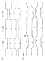
制御回路240は、上記のトランジスターQ1〜Q4をオン・オフ制御する回路であり、そのオン・オフ制御のための第1〜第4の駆動パルス信号S1〜S4を出力する。図2(A)に、駆動パルス信号S1〜S4の波形例を示す。
The
この例では、駆動パルス信号S1〜S4はローアクティブの信号である。即ち、チャージ期間において、駆動パルス信号S1、S4はローレベルであり、駆動パルス信号S2、S3はハイレベルである。このチャージ期間では、図3に示すように、トランジスターQ1、Q4はオンし、トランジスターQ2、Q3はオフし、電源からグランドへ駆動電流Idが流れる。一方、ディケイ期間において、駆動パルス信号S1、S4はハイレベルであり、駆動パルス信号S2、S3はローレベルである。この期間では、図4に示すように、トランジスターQ1、Q4はオフし、トランジスターQ2、Q3はオンし、グランドから電源へ駆動電流Idが回生する。 In this example, the drive pulse signals S1 to S4 are low active signals. That is, in the charge period, the drive pulse signals S1 and S4 are at a low level, and the drive pulse signals S2 and S3 are at a high level. In this charge period, as shown in FIG. 3, the transistors Q1 and Q4 are turned on, the transistors Q2 and Q3 are turned off, and the drive current Id flows from the power supply to the ground. On the other hand, during the decay period, the drive pulse signals S1 and S4 are at a high level, and the drive pulse signals S2 and S3 are at a low level. In this period, as shown in FIG. 4, the transistors Q1 and Q4 are turned off, the transistors Q2 and Q3 are turned on, and the drive current Id is regenerated from the ground to the power source.
図12で後述のように、チャージ期間ではモーター280の駆動電流Idが増加し、ディケイ期間ではモーター280の駆動電流Idが減少する。制御回路240は、これらの期間を繰り返し、その期間の長さを制御することで駆動電流Id(即ちモーターの回転数)を制御する。
As will be described later with reference to FIG. 12, the drive current Id of the
遅延部250は、駆動パルス信号S1〜S4を遅延させる第1〜第4の遅延回路251〜254を含む。具体的には、レジスター部235は、第1〜第4の遅延時間情報が可変に設定される遅延設定レジスター237を含む。そして、遅延回路251〜254は、それぞれ第1〜第4の遅延時間情報に基づいて駆動パルス信号S1〜S4を遅延させ、遅延された駆動パルス信号SD1〜SD4を出力する。ここで、第1〜第4の遅延時間情報は、遅延時間に対応する情報であれば、どのような情報であってもよい。例えば、後述の実施形態では、クロックを用いて遅延を発生させるが、その遅延するクロック数を遅延時間情報としてもよい。或は、遅延時間そのものや、遅延時間を符号化した情報等であってもよい。
The
プリドライバー部260は、第1〜第4のトランジスターQ1〜Q4を駆動する第1〜第4のプリドライバー261〜264を含む。プリドライバー261〜264は、遅延された駆動パルス信号SD1〜SD4をバッファリングし、駆動信号G1〜G4としてトランジスターQ1〜Q4のゲートへ出力する。
The
さて、比較例として遅延部250が設けられていない回路装置200を考える。この比較例では、制御回路240から出力された駆動パルス信号S1〜S4は、直接プリドライバー261〜264によりバッファリングされ、駆動信号G1〜G4として出力される。図2(A)に示すように、駆動パルス信号S1〜S4ではオン・オフが切り替わるタイミングが揃っている。この理想的なタイミングのままトランジスターQ1〜Q4に印加されれば、図3、図4に示すように、直列に接続されたトランジスターQ1、Q2(又はQ3、Q4)は排他的にオン・オフする。この場合には、トランジスターQ1、Q2(又はQ3、Q4)を通じた電源電圧VCCからグランド電圧への貫通電流は生じない。
Now, consider a
しかしながら、例えばプリドライバー261〜264の駆動能力やトランジスターQ1〜Q4のゲートサイズ、負荷であるモーター280の特性等によって、実際にトランジスターQ1〜Q4のオン・オフが切り替わるタイミングは駆動パルス信号S1〜S4とは異なるものとなる。
However, the timing at which the transistors Q1 to Q4 are actually switched on / off depending on, for example, the driving capability of the
図2(B)に、比較例における駆動信号G1〜G4の波形例を示す。この例では、ハイサイド側のトランジスターQ1、Q3を駆動する駆動信号G1、G3と、ローサイド側のトランジスターQ2、Q4を駆動する駆動信号G2、G4とで、エッジの傾き(立ち上がり時間、立ち下がり時間)が異なっている。エッジの傾きは、オン・オフの切り替えタイミングを遅延させるので、ハイサイド側とローサイド側でタイミングがずれ、トランジスターQ1、Q2(又はQ3、Q4)が同時にオンする期間TTが発生する。この期間TTでは電源とグランドがショートするため貫通電流が生じる。 FIG. 2B shows a waveform example of the drive signals G1 to G4 in the comparative example. In this example, the drive signals G1 and G3 for driving the high-side transistors Q1 and Q3 and the drive signals G2 and G4 for driving the low-side transistors Q2 and Q4 have edge gradients (rise time, fall time). ) Is different. Since the edge inclination delays the ON / OFF switching timing, the timing is shifted between the high side and the low side, and a period TT in which the transistors Q1 and Q2 (or Q3 and Q4) are simultaneously turned on is generated. During this period TT, the power supply and the ground are short-circuited, and a through current is generated.
そこで本実施形態では、遅延回路251〜254が、遅延設定レジスター237に設定された第1〜第4の遅延時間情報に対応する第1〜第4の遅延時間TD1〜TD4だけ、駆動パルス信号S1〜S4を遅延させる。図5に、遅延回路251〜254が出力する駆動パルス信号SD1〜SD4の波形例と、その駆動パルス信号SD1〜SD4に基づいてプリドライバー261〜264が出力する駆動信号G1〜G4の波形例を示す。
Therefore, in the present embodiment, the
図5に示すように、遅延回路251〜254は、トランジスターQ1〜Q4をオフからオンにする際の駆動パルス信号S1〜S4を、遅延時間TD1〜TD4だけ遅延させる。ローアクティブの場合、ハイレベルからローレベルに変化する立ち下がりエッジが遅延される。即ち、チャージ期間からディケイ期間に移行する際には、駆動パルス信号SD1、SD4の立ち上がりエッジに対して、駆動パルス信号SD2、SD3の立ち下がりエッジが遅延する。一方、ディケイ期間からチャージ期間に移行する際には、駆動パルス信号SD2、SD3の立ち上がりエッジに対して、駆動パルス信号SD1、SD4の立ち下がりエッジが遅延する。
As shown in FIG. 5, the
この駆動パルス信号SD1〜SD4の遅延により、例えばトランジスターQ2がオフからオンになるタイミングが遅延時間TD2だけ遅延する。このようにオフからオンになるタイミングを遅延させたことによって、トランジスターQ1がオフになるのを待ってからトランジスターQ2をオンさせることが可能となる。即ち、直列に接続されるトランジスターQ1、Q2が同時オフになる期間が生まれ、これによって、図2(B)で説明したような同時オンになる期間TTを無くし、貫通電流を回避できる。
Due to the delay of the drive pulse signals SD1 to SD4, for example, the timing at which the transistor Q2 is turned on is delayed by a delay time TD2. Thus, by delaying the timing of turning on from off, it is possible to turn on the transistor Q2 after waiting for the transistor Q1 to turn off. That is, born period transistors Q1, Q2 connected in series is simultaneously turned off, thereby, eliminate the period TT composed simultaneously on as described in FIG. 2 (B), the can be avoided through current.
次に、第2の比較例として、トランジスターQ1〜Q4が全てオフとなる固定期間を設ける場合を考える。図6に、第2の比較例における波形例を示す。駆動パルス信号SD1〜SD4には、全てハイレベルとなる固定期間が設けられている。その期間に対応して、駆動信号G1〜G4には、トランジスターQ1〜Q4を全てオフにする期間が生じる。 Next, as a second comparative example, consider a case where a fixed period in which all the transistors Q1 to Q4 are turned off is provided. FIG. 6 shows a waveform example in the second comparative example. The drive pulse signals SD1 to SD4 are all provided with a fixed period that is at a high level. Corresponding to this period, the drive signals G1 to G4 have a period in which all the transistors Q1 to Q4 are turned off.
実際にトランジスターQ1〜Q4のオン・オフが切り替わるタイミングは、上述のように種々の要因で変動するので、その変動の最悪の条件に合わせて、駆動パルス信号SD1〜SD4を全てハイレベルにする固定期間を設定しておく必要がある。そのため、トランジスターQ1〜Q4が全てオフする期間が長くなり、オンする期間が削られるので、例えば電力効率の低下やモーター280のトルク低下等を招くという課題がある。
The timing at which the transistors Q1 to Q4 are actually switched on and off varies depending on various factors as described above. Therefore, the drive pulse signals SD1 to SD4 are all set to a high level in accordance with the worst condition of the variation. It is necessary to set a period. Therefore, the period during which all the transistors Q1 to Q4 are turned off becomes longer and the time during which the transistors Q1 to Q4 are turned on is reduced. For example, there is a problem in that power efficiency is reduced and torque of the
上述した特許文献1では、駆動信号をモニターした結果に基づいてトランジスターのオン・オフのタイミングが制御されるため、デッドタイムは固定ではない。しかしながら、トランジスターのオン・オフのタイミングを自由に設定することはできないので、デッドタイムを最適化することはできない。
In
この点、本実施形態では、トランジスターQ1〜Q4に対応する遅延時間TD1〜TD4は、遅延設定レジスター237により、それぞれ独立に調整することができる。例えば、製造時において回路装置200とモーター280を組み合わせ、貫通電流を発生させない最小限の遅延時間TD1〜TD4を測定し、それに対応する遅延時間情報を遅延設定レジスター237に設定しておく。或は、その作業をユーザーが行ってもよい。
In this regard, in this embodiment, the delay times TD1 to TD4 corresponding to the transistors Q1 to Q4 can be independently adjusted by the
これにより、必要最小限の遅延時間TD1〜TD4を設定できるので、最適なデッドタイムが設定され、電力効率の低下やモーター280のトルク低下等を抑制できる。本来、直列に接続されたトランジスターQ1、Q2(又はQ3、Q4)が同時にオンしなければ良いので、全てのトランジスターQ1〜Q4を同時にオフにする必要はない。本実施形態では、例えば図5の駆動信号G2、G3の遅延時間TD2、TD3を個別に調整できるので、トランジスターQ1、Q2の関係と、トランジスターQ3、Q4の関係が個別に調整される。即ち、全て同時オフという制約がないので、可能な限りデッドタイムを削減してトランジスターがオンする時間を増やすことができる。
Thereby, since the minimum necessary delay times TD1 to TD4 can be set, an optimum dead time is set, and a reduction in power efficiency, a reduction in torque of the
なお、上記の実施形態ではブリッジ回路210を第1〜第4のトランジスターQ1〜Q4(Hブリッジ)で構成する場合を例に説明したが、ブリッジ回路210は第1〜第nのトランジスター(nは2以上)で構成されればよい。例えば、ブリッジ回路210をハーフブリッジで構成してもよい。この場合、例えばブリッジ回路210をトランジスターQ1、Q2で構成し、端子OUT2をグランド電圧に接続する。
In the above embodiment, the case where the
2.遅延時間の設定手法
次に、具体的なブリッジ回路210の構成における遅延時間TD1〜TD4の設定手法について説明する。
2. Next, a method for setting the delay times TD1 to TD4 in the specific configuration of the
図1に示す構成例のブリッジ回路210では、ハイサイド側のトランジスターQ1、Q3は、P型トランジスターであり、ローサイド側のトランジスターQ2、Q4は、N型トランジスターである。ここで、ハイサイド側のトランジスターとは、ローサイド側のトランジスターよりも高電位電源側に接続されるトランジスターであり、ローサード側のトランジスターとは、ハイサイド側のトランジスターよりも低電位電源側に接続されるトランジスターである。
In the
ブリッジ回路210は、高電圧の電源電圧VCC(例えば42V)で動作する。一方、制御回路240や遅延部250は、低電圧の電源電圧(例えば5V)で動作するため、プリドライバー261〜264は、駆動パルス信号SD1〜SD4の信号レベルを変換するレベルシフターで構成される。ハイサイド側がP型トランジスター、ローサイド側がN型トランジスターであることに伴い、プリドライバー261、263は、入力信号(SD1、SD3)を正転論理で出力し、プリドライバー262、264は、入力信号(SD2、SD4)を反転論理で出力する。
The
このような構成とすることで、図5に示すように、P型トランジスターQ1、Q3にはローアクティブの駆動信号G1、G3を供給し、N型トランジスターQ2、Q4にはハイアクティブの駆動信号G2、G4を供給することができる。その一方で、駆動パルス信号SD1〜SD4をローアクティブに揃えることができるので、遅延回路251〜254の回路構成を共通化することができる。これにより、例えば遅延回路251〜254の設計を簡素化すること等が可能となる。なお、遅延回路251〜254の詳細な構成については後述する。
With such a configuration, as shown in FIG. 5, low-active drive signals G1 and G3 are supplied to the P-type transistors Q1 and Q3, and high-active drive signals G2 are supplied to the N-type transistors Q2 and Q4. , G4 can be supplied. On the other hand, since the drive pulse signals SD1 to SD4 can be made low active, the circuit configurations of the
図5に示すように、遅延設定レジスター237には、ハイサイド側のP型トランジスターQ1をオフからオンにする際の第1の遅延時間TD1よりも、ローサイド側のN型トランジスターQ2をオフからオンにする際の第2の遅延時間TD2が長くなるように(即ちTD2>TD1)、第1の遅延時間情報と第2の遅延時間情報が設定される。
As shown in FIG. 5, in the
この点について、図7(A)〜図8(B)を用いて説明する。図7(A)、図7(B)に、ハイサイド側のP型トランジスターQ1についての波形例を示す。この波形例は、グランドと端子OUT1の間に負荷として抵抗素子を接続し、駆動パルス信号SD1と端子OUT1の電圧を測定したものである。また、図8(A)、図8(B)に、ローサイド側のN型トランジスターQ2についての波形例を示す。この波形例は、電源と端子OUT1の間に負荷として抵抗素子を接続し、駆動パルス信号SD2と端子OUT1の電圧を測定したものである。なお、P型トランジスターQ3、N型トランジスターQ4についても同様の波形となる。 This point will be described with reference to FIGS. 7A to 8B. FIG. 7A and FIG. 7B show waveform examples for the high-side P-type transistor Q1. In this waveform example, a resistance element is connected as a load between the ground and the terminal OUT1, and the voltage of the drive pulse signal SD1 and the terminal OUT1 is measured. 8A and 8B show waveform examples of the low-side N-type transistor Q2. In this waveform example, a resistance element is connected as a load between the power supply and the terminal OUT1, and the voltage of the drive pulse signal SD2 and the terminal OUT1 is measured. The same waveform is obtained for the P-type transistor Q3 and the N-type transistor Q4.
駆動パルス信号SD1が立ち下がってから、P型トランジスターQ1の出力が立ち上がる(オンになる)時間はTrp=744ns、駆動パルス信号SD1が立ち上がってから、P型トランジスターQ1の出力が立ち下がる(オフになる)時間はTfp=688nsである。また、駆動パルス信号SD2が立ち下がってから、N型トランジスターQ2の出力が立ち下がる(オンになる)時間はTfn=464ns、駆動パルス信号SD2が立ち上がってから、N型トランジスターQ2の出力が立ち上がる(オフになる)時間はTrn=688nsである。 The time when the output of the P-type transistor Q1 rises (turns on) after the drive pulse signal SD1 falls is Trp = 744 ns, and after the drive pulse signal SD1 rises, the output of the P-type transistor Q1 falls (turns off) The time is Tfp = 688 ns. Also, the time when the output of the N-type transistor Q2 falls (turns on) after the drive pulse signal SD2 falls is Tfn = 464 ns, and after the drive pulse signal SD2 rises, the output of the N-type transistor Q2 rises ( The time to turn off is Trn = 688 ns.
これらの立ち上がり・立ち下がり時間の間には、Trp>Trn、Tfp>Tfnの関係がある。ブリッジ回路210では、トランジスターQ1〜Q4のオン抵抗が電力効率に影響するので、トランジスターサイズを大きくしてオン抵抗を下げることが望ましい。一般に、P型トランジスターはN型トランジスターに比べてオン抵抗が大きいので、Trp>Trn、Tfp>Tfnとなる。
There is a relationship of Trp> Trn and Tfp> Tfn between these rise / fall times. In the
図5に示すように、ディケイ期間からチャージ期間に移行する際には、Trp>Trnに対応して、トランジスターQ1がオフからオンになる時間(Trp)は、トランジスターQ2がオンからオフになる時間(Trn)よりも長い。即ち、遅延時間を設けなくても、同時にオンする可能性は低い。この場合、遅延時間TD1は、例えばゼロに設定してもよいし、或は念のため小さい値に設定しておけばよい。 As shown in FIG. 5, when transitioning from the decay period to the charge period, the time when the transistor Q1 is turned on from off (Trp) corresponds to Trp> Trn. Longer than (Trn). That is, even if no delay time is provided, the possibility of turning on at the same time is low. In this case, the delay time TD1 may be set to zero, for example, or may be set to a small value just in case.
一方、チャージ期間からディケイ期間に移行する際には、Tfp>Tfnに対応して、トランジスターQ2がオフからオンになる時間(Tfn)は、トランジスターQ1がオンからオフになる時間(Tfp)よりも短い。即ち、遅延時間を設けないと同時にオンする可能性は高い。そのため、遅延時間TD2は、遅延時間TD1よりも長い時間に設定する必要がある。 On the other hand, when shifting from the charge period to the decay period, the time when the transistor Q2 is turned on from off (Tfn) corresponds to Tfp> Tfn than the time when the transistor Q1 is turned on from off (Tfp). short. That is, there is a high possibility that the delay time is not provided and at the same time. Therefore, the delay time TD2 needs to be set longer than the delay time TD1.
以上のように遅延時間TD1、TD2を設定することで、ハイサイド側をP型トランジスターで構成し、ローサイド側をN型トランジスターで構成したブリッジ回路210に対して、適切な遅延時間TD1、TD2を設定することができる。即ち、遅延時間TD1、TD2をプログラマブルに個々に設定できることにより、上記のような具体的なブリッジ回路210の構成に対して、貫通電流を回避できる必要最小限のデッドタイムを実現できる。
By setting the delay times TD1 and TD2 as described above, appropriate delay times TD1 and TD2 are set for the
なお、上記ではトランジスターQ1、Q2について説明したが、トランジスターQ3、Q4についても同様である。即ち、遅延設定レジスター237には、ハイサイド側のP型トランジスターQ3をオフからオンにする際の第3の遅延時間TD3よりも、ローサイド側のN型トランジスターQ4をオフからオンにする際の第4の遅延時間TD4が長くなるように(即ちTD4>TD3)、第3の遅延時間情報と第4の遅延時間情報が設定される。例えば、TD3=TD1、TD4=TD2に設定する。トランジスターQ1、Q2とトランジスターQ3、Q4では、チャージ期間及びディケイ期間との関係が入れ替わるだけであり、トランジスターQ1、Q2を例に上述した内容についてはトランジスターQ3、Q4についても同様に成り立つ。
Although the transistors Q1 and Q2 have been described above, the same applies to the transistors Q3 and Q4. That is, in the
3.遅延回路
次に、遅延回路251〜254の詳細について説明する。
3. Delay Circuit Next, details of the
遅延設定レジスター237には、第1〜第4の遅延時間情報として、第1〜第4のクロック数が設定される。即ち、第1〜第4のクロック数に対応する時間が、遅延時間TD1〜TD4となる。そして、遅延回路251〜254は、トランジスターQ1〜Q4をオフからオンにする際の駆動パルス信号S1〜S4を、遅延設定レジスター237に設定された第1〜第4のクロック数だけ遅延させ、その遅延させた駆動パルス信号SD1〜SD4を出力する。遅延に用いるクロック信号は、例えば外部のホストコントローラーから供給されるシステムクロック信号であってもよいし、或は、回路装置200内部のクロック生成回路で生成したクロック信号であってもよい。
In the
このようにすれば、遅延時間TD1〜TD4をクロック数で規定できるので、バラツキのない遅延時間TD1〜TD4を設定することが可能となり、正確に最小限のデッドタイムを設定することができる。また、駆動パルス信号S1〜S4のエッジを遅延させれば良いだけなので、例えば入力信号のエッジの手前に新たなエッジを作る必要がある場合に比べて、遅延回路の構成を簡素化することができる。 In this way, since the delay times TD1 to TD4 can be defined by the number of clocks, it is possible to set the delay times TD1 to TD4 without variations, and it is possible to accurately set the minimum dead time. Further, since it is only necessary to delay the edges of the drive pulse signals S1 to S4, for example, the configuration of the delay circuit can be simplified as compared with a case where a new edge needs to be created before the edge of the input signal. it can.
図9に、遅延回路251の詳細な構成例を示す。また図10に、遅延回路251の詳細な構成例におけるタイミングチャートを示す。なお、以下では第iの遅延回路(iはn=4以下の自然数)として第1の遅延回路251を例に説明するが、第2〜第4の遅延回路252〜254も同様に構成できる。
FIG. 9 shows a detailed configuration example of the
遅延回路251は、第1〜第4のフリップフロップ回路FF1〜FF4(広義には第1〜第kのフリップフロップ回路)、セレクターSEL1、論理和回路OR1(広義には論理回路)を含む。
The
フリップフロップ回路FF1〜FF4はカスケードに接続されており、フリップフロップ回路FF1〜FF4にはクロック信号CLKが入力される。具体的には、フリップフロップ回路FF1には、駆動パルス信号S1が入力される。図10に示すように、フリップフロップ回路FF1は、駆動パルス信号S1をクロック信号CLKの1周期(1発)分だけ遅延させた遅延パルス信号QF1を出力する。その遅延パルス信号QF1は、フリップフロップ回路FF2に入力される。図10に示すように、フリップフロップ回路FF2は、遅延パルス信号QF1を更にクロック信号CLKの1周期分だけ遅延させた遅延パルス信号QF2を出力する。以降、フリップフロップ回路FF3、FF4も同様にカスケードに接続される。このようにして、フリップフロップ回路FF1〜FF4は、それぞれクロック1周期〜4周期分だけ駆動パルス信号S1を遅延させた遅延パルス信号QF1〜QF4を出力する。 The flip-flop circuits FF1 to FF4 are connected in cascade, and the clock signal CLK is input to the flip-flop circuits FF1 to FF4. Specifically, the drive pulse signal S1 is input to the flip-flop circuit FF1. As shown in FIG. 10, the flip-flop circuit FF1 outputs a delayed pulse signal QF1 obtained by delaying the drive pulse signal S1 by one cycle (one shot) of the clock signal CLK. The delayed pulse signal QF1 is input to the flip-flop circuit FF2. As shown in FIG. 10, the flip-flop circuit FF2 outputs a delayed pulse signal QF2 obtained by further delaying the delayed pulse signal QF1 by one cycle of the clock signal CLK. Thereafter, the flip-flop circuits FF3 and FF4 are similarly connected in cascade. In this way, the flip-flop circuits FF1 to FF4 output delayed pulse signals QF1 to QF4 obtained by delaying the drive pulse signal S1 by 1 to 4 clock cycles, respectively.
セレクターSEL1には、遅延パルス信号QF1〜QF4とセレクト信号SELが入力される。セレクト信号SELは、遅延設定レジスター237に設定された第1の遅延時間情報であり、第1の遅延時間TD1に対応するクロック数である。図10に示すように、例えばクロック数としてSEL=3が設定されたとする。この場合、セレクターSEL1は、遅延パルス信号QF3を選択し、信号QS1として出力する。
Delay pulse signals QF1 to QF4 and a select signal SEL are input to the selector SEL1. The select signal SEL is first delay time information set in the
論理和回路OR1には、駆動パルス信号S1と信号QS1が入力され、論理和回路OR1は、これらの信号の論理和をとり、遅延された駆動パルス信号SD1として出力する。このとき、論理和回路OR1は、トランジスターQ1をオフからオンにする場合のエッジとして、セレクターSEL1が選択した遅延パルス信号QS1のエッジを出力する。即ち、図10に示すように、駆動パルス信号S1がハイレベルからローレベルになる場合、信号QS1がハイレベルからローレベルになるタイミングで、駆動パルス信号SD1はハイレベルからローレベルになる。一方、駆動パルス信号S1がローレベルからハイレベルになる場合、駆動パルス信号S1がローレベルからハイレベルになるタイミングで、駆動パルス信号SD1はローレベルからハイレベルになる。このように、駆動パルス信号SD1の立ち下がりエッジは信号QS1と同様に遅延し、立ち上がりエッジは遅延しない。 The drive pulse signal S1 and the signal QS1 are input to the OR circuit OR1, and the OR circuit OR1 takes a logical sum of these signals and outputs it as a delayed drive pulse signal SD1. At this time, the OR circuit OR1 outputs the edge of the delayed pulse signal QS1 selected by the selector SEL1 as an edge when the transistor Q1 is turned on from off. That is, as shown in FIG. 10, when the drive pulse signal S1 changes from the high level to the low level, the drive pulse signal SD1 changes from the high level to the low level at the timing when the signal QS1 changes from the high level to the low level. On the other hand, when the drive pulse signal S1 changes from low level to high level, the drive pulse signal SD1 changes from low level to high level at the timing when the drive pulse signal S1 changes from low level to high level. As described above, the falling edge of the drive pulse signal SD1 is delayed similarly to the signal QS1, and the rising edge is not delayed.
以上のように遅延回路251〜254を構成することで、遅延設定レジスター237に設定された第1〜第4のクロック数だけ、トランジスターQ1〜Q4をオフからオンにする際の第1〜第4の駆動パルス信号S1〜S4を遅延させることができる。即ち、セレクターSEL1により、各遅延回路で個別にクロック数に応じて遅延パルス信号QF1〜QF4のいずれかを選択できる。そして、その選択された信号QS1の立ち下がりエッジのみを、論理和回路OR1により駆動パルス信号SD1〜SD4に反映させることができる。
By configuring the
なお、以上の実施形態では駆動パルス信号S1〜S4や駆動パルス信号SD1〜SD4がローアクティブの信号である場合を例に説明したが、これらの信号はハイアクティブの信号であってもよい。この場合、例えば、遅延回路251〜254の論理和回路OR1を論理積回路に変更し、プリドライバー261、263を反転論理のレベルシフターで構成し、プリドライバー262、264を正転論理のレベルシフターで構成する。
In the above embodiment, the case where the drive pulse signals S1 to S4 and the drive pulse signals SD1 to SD4 are low active signals has been described as an example. However, these signals may be high active signals. In this case, for example, the logical sum circuit OR1 of the
4.回路装置の詳細構成
図11に、回路装置200の詳細な構成例を示す。また図12に、回路装置200の詳細な構成例における動作説明図を示す。
4). Detailed Configuration of Circuit Device FIG. 11 shows a detailed configuration example of the
図11の回路装置200は、ブリッジ回路210、コンパレーター221(検出回路)、基準電圧生成回路230、レジスター部235、制御回路240、遅延部250、プリドライバー部260、クロック生成回路270を含む。なお、既に上述した構成要素と同一の構成要素については同一の符号を付し、適宜説明を省略する。
11 includes a
クロック生成回路270は、クロック信号CLKを生成し、そのクロック信号CLKを回路装置200の各部へ供給する。遅延回路251〜254は、クロック信号CLKを受けて、遅延された駆動パルス信号SD1〜SD4を生成する。
The
ブリッジ回路210において、ローサイド側のトランジスターQ2、Q4のソースノードは、端子RNFに接続されたノードN1に接続される。端子RNFには、センス抵抗290の一端が接続される。センス抵抗290の他端はグランド電圧のノードに接続される。
In the
レジスター部235は、上述した遅延設定レジスター237と、ディケイ期間の長さが設定される期間設定レジスター236と、チャージ電流(駆動電流Id)の上限が設定される上限設定レジスター238と、を含む。レジスター部235には、例えばホストコントローラー(例えばCPU)がレジスター値を可変に書き込み、これによりホストコントローラーがモーター280の回転数やトルク等を制御する。
The
基準電圧生成回路230は、チャージ電流の上限Imaxを検出するための基準電圧VRを生成する。具体的には、基準電圧生成回路230はD/A変換回路で構成される。D/A変換回路は、リファレンス電圧Vrefに基づいて複数の電圧を生成し、その複数の電圧の中から、上限設定レジスター238に設定されたレジスター値に対応する電圧を選択し、その選択した電圧を基準電圧VRとして出力する。
The reference
コンパレーター221は、ノードN1の電圧VSを検出することで、チャージ期間でのチャージ電流を検出する。図3に示すように、駆動電流Idは、電源電圧VCCからトランジスターQ1、モーター280、トランジスターQ4へ流れる。図11の構成例では、更にセンス抵抗290を経由し、グランド電圧へ流れる。このチャージ期間における駆動電流Idを、チャージ電流と呼ぶ。図12に示すように、チャージ期間TCではチャージ電流は増加し、その増加と共にノードN1の電圧VSが上昇する。コンパレーター221は、電圧VSが基準電圧VRに達したことを検出することで、チャージ電流が上限Imaxに達したことを検出する。
The
制御回路240は、チャージ期間TCにおいてコンパレーター221がチャージ電流の上限Imaxを検出した場合に、チャージ期間TCからディケイ期間TDに切り替える。ディケイ期間TDにおける駆動電流Idをディケイ電流と呼び、図12に示すように、ディケイ期間TDではディケイ電流は減少する。制御回路240は、ディケイ期間TDに切り替えてから、期間設定レジスター236に設定されたディケイ期間が経過した後、ディケイ期間TDからチャージ期間TCに切り替える。以上のようにして、チャージ期間TCとディケイ期間TDが繰り返され、モーター280の駆動電流Idは、上限がImaxとなるように制御される。
The
5.電子機器
図13に、本実施形態の回路装置200が適用された電子機器の構成例を示す。電子機器は、処理部300、記憶部310、操作部320、入出力部330、回路装置200、これらの各部を接続するバス340、モーター280を含む。回路装置200は、例えば集積回路装置により実現できる。以下ではモーター駆動によりヘッドや紙送りを制御するプリンターを例にとり説明するが、本実施形態はこれに限定されず、種々の電子機器に適用可能である。
5. Electronic Device FIG. 13 shows a configuration example of an electronic device to which the
入出力部330は例えばUSBコネクターや無線LAN等のインターフェースで構成され、画像データや文書データが入力される。入力されたデータは、例えばDRAM等の内部記憶装置である記憶部310に記憶される。操作部320により印刷指示を受け付けると、処理部300は、記憶部310に記憶されたデータの印刷動作を開始する。処理部300は、データの印刷レイアウトに合わせて回路装置200に指示を送り、回路装置200は、その指示に基づいてモーター280を回転させ、ヘッドの移動や紙送りを行う。
The input /
なお、上記のように本実施形態について詳細に説明したが、本発明の新規事項および効果から実体的に逸脱しない多くの変形が可能であることは当業者には容易に理解できるであろう。従って、このような変形例はすべて本発明の範囲に含まれるものとする。例えば、明細書又は図面において、少なくとも一度、より広義または同義な異なる用語と共に記載された用語は、明細書又は図面のいかなる箇所においても、その異なる用語に置き換えることができる。また本実施形態及び変形例の全ての組み合わせも、本発明の範囲に含まれる。また遅延回路、ブリッジ回路、回路装置、電子機器の構成・動作や、遅延時間の設定手法、ブリッジ回路の制御手法等も、本実施形態で説明したものに限定されず、種々の変形実施が可能である。 Although the present embodiment has been described in detail as described above, it will be easily understood by those skilled in the art that many modifications can be made without departing from the novel matters and effects of the present invention. Accordingly, all such modifications are intended to be included in the scope of the present invention. For example, a term described at least once together with a different term having a broader meaning or the same meaning in the specification or the drawings can be replaced with the different term in any part of the specification or the drawings. All combinations of the present embodiment and the modified examples are also included in the scope of the present invention. Also, the configuration and operation of the delay circuit, bridge circuit, circuit device, electronic device, delay time setting method, bridge circuit control method, etc. are not limited to those described in this embodiment, and various modifications can be made. It is.
200 回路装置、210 ブリッジ回路、221 コンパレーター、
230 基準電圧生成回路、235 レジスター部、236 期間設定レジスター、
237 遅延設定レジスター、238 上限設定レジスター、240 制御回路、
250 遅延部、251〜254 第1〜第4の遅延回路、
260 プリドライバー部、261〜264 第1〜第4のプリドライバー、
270 クロック生成回路、280 モーター、290 センス抵抗、
300 処理部、310 記憶部、320 操作部、330 入出力部、340 バス、
CLK クロック信号、D1〜D4 ダイオード、
FF1〜FF4 第1〜第4のフリップフロップ回路、
G1〜G4 第1〜第4の駆動信号、Id 駆動電流、Imax 上限、
OR1 論理和回路、OUT1,OUT2 端子、
Q1〜Q4 第1〜第4のトランジスター、QF1〜QF4 遅延パルス信号、
RNF 端子、S1〜S4 第1〜第4の駆動パルス信号、
SD1〜SD4 遅延された第1〜第4の駆動パルス信号、
SEL セレクト信号、SEL1 セレクター、TC チャージ期間、
TD ディケイ期間、TD1〜TD4 第1〜第4の遅延時間
200 circuit device, 210 bridge circuit, 221 comparator,
230 reference voltage generation circuit, 235 register section, 236 period setting register,
237 delay setting register, 238 upper limit setting register, 240 control circuit,
250 delay units, 251 to 254, first to fourth delay circuits,
260 pre-driver units, 261 to 264, first to fourth pre-drivers,
270 clock generation circuit, 280 motor, 290 sense resistor,
300 processing unit, 310 storage unit, 320 operation unit, 330 input / output unit, 340 bus,
CLK clock signal, D1-D4 diode,
FF1 to FF4 first to fourth flip-flop circuits,
G1 to G4 1st to 4th drive signals, Id drive current, Imax upper limit,
OR1 OR circuit, OUT1 and OUT2 terminals,
Q1-Q4 first to fourth transistors, QF1-QF4 delayed pulse signals,
RNF terminal, S1 to S4, first to fourth drive pulse signals,
SD1 to SD4 Delayed first to fourth drive pulse signals,
SEL select signal, SEL1 selector, TC charge period,
TD decay period, TD1 to TD4 1st to 4th delay time
Claims (7)
前記第1のハイサイドトランジスターをオン・オフ制御する第1の駆動パルス信号を出力し、前記第1のローサイドトランジスターをオン・オフ制御する第2の駆動パルス信号を出力し、前記第2のハイサイドトランジスターをオン・オフ制御する第3の駆動パルス信号を出力し、前記第2のローサイドトランジスターをオン・オフ制御する第4の駆動パルス信号を出力する制御回路と、
前記第1の駆動パルス信号を第1の遅延時間情報に基づいて第1の遅延時間遅延させる第1の遅延回路と、
前記第2の駆動パルス信号を第2の遅延時間情報に基づいて第2の遅延時間遅延させる第2の遅延回路と、
前記第3の駆動パルス信号を第3の遅延時間情報に基づいて第3の遅延時間遅延させる第3の遅延回路と、
前記第4の駆動パルス信号を第4の遅延時間情報に基づいて第4の遅延時間遅延させる第4の遅延回路と、
遅延された前記第1の駆動パルス信号に基づいて、前記第1のハイサイドトランジスターを駆動する第1のプリドライバーと、
遅延された前記第2の駆動パルス信号に基づいて、前記第1のローサイドトランジスターを駆動する第2のプリドライバーと、
遅延された前記第3の駆動パルス信号に基づいて、前記第2のハイサイドトランジスターを駆動する第3のプリドライバーと、
遅延された前記第4の駆動パルス信号に基づいて、前記第2のローサイドトランジスターを駆動する第4のプリドライバーと、
前記第1の遅延時間情報、前記第2の遅延時間情報、前記第3の遅延時間情報及び前記第4の遅延時間情報が保存される遅延設定レジスターと、
を含み、
前記遅延設定レジスターには、
前記第2のハイサイドトランジスターをオフからオンにする際の前記第3の遅延時間よりも前記第1のローサイドトランジスターをオフからオンにする際の前記第2の遅延時間が長くなるように、前記第3の遅延時間情報と前記第2の遅延時間情報が設定され、
前記第1のハイサイドトランジスターをオフからオンにする際の前記第1の遅延時間よりも前記第2のローサイドトランジスターをオフからオンにする際の前記第4の遅延時間が長くなるように、前記第1の遅延時間情報と前記第4の遅延時間情報が設定され、
前記第1の遅延時間より前記第2の遅延時間が長くなるように、前記第1の遅延時間情報と前記第2の遅延時間情報が設定され、
前記第3の遅延時間より前記第4の遅延時間が長くなるように、前記第3の遅延時間情報と前記第4の遅延時間情報が設定されることを特徴とする回路装置。 A P-type first high-side transistor and an N-type first low-side transistor connected in series between a first power-supply potential and a second power-supply potential lower than the first power-supply potential; An H-bridge circuit having a P-type second high-side transistor and an N-type second low-side transistor connected in series between the first power supply potential and the second power supply potential;
A first drive pulse signal for controlling on / off of the first high side transistor is output, a second drive pulse signal for controlling on / off of the first low side transistor is output, and the second high pulse is output. A control circuit for outputting a third drive pulse signal for controlling on / off of the side transistor, and for outputting a fourth drive pulse signal for controlling on / off of the second low-side transistor;
A first delay circuit for delaying the first drive pulse signal based on first delay time information by a first delay time;
A second delay circuit for delaying the second drive pulse signal based on second delay time information by a second delay time;
A third delay circuit for delaying the third drive pulse signal based on third delay time information by a third delay time;
A fourth delay circuit for delaying the fourth drive pulse signal based on fourth delay time information by a fourth delay time;
A first pre-driver for driving the first high-side transistor based on the delayed first drive pulse signal;
A second pre-driver for driving the first low-side transistor based on the delayed second drive pulse signal;
A third pre-driver for driving the second high-side transistor based on the delayed third driving pulse signal;
A fourth pre-driver for driving the second low-side transistor based on the delayed fourth drive pulse signal;
A delay setting register for storing the first delay time information, the second delay time information, the third delay time information, and the fourth delay time information;
Including
In the delay setting register,
The second delay time when turning on the first low-side transistor from off to on is longer than the third delay time when turning on the second high-side transistor from off to on. Third delay time information and the second delay time information are set,
The fourth delay time when turning on the second low-side transistor from off to on is longer than the first delay time when turning on the first high-side transistor from off to on. First delay time information and the fourth delay time information are set ,
The first delay time information and the second delay time information are set so that the second delay time is longer than the first delay time,
It said third delay such that the time becomes longer than said fourth delay time of the third and the fourth delay time information and delay time information is set circuit device according to claim Rukoto.
前記遅延設定レジスターには、
前記第1〜第4の遅延時間情報として第1〜第4のクロック数が設定され、
前記第1〜第4の遅延回路は、
前記第1〜第4のクロック数だけ、前記第1〜第4のトランジスターをオフからオンにする際の前記第1〜第4の駆動パルス信号を遅延させることを特徴とする回路装置。 In claim 1,
In the delay setting register,
First to fourth clock numbers are set as the first to fourth delay time information,
The first to fourth delay circuits are
The circuit device characterized by delaying the first to fourth drive pulse signals when the first to fourth transistors are turned on from off to the number of first to fourth clocks.
前記第1〜第4の遅延回路のうち第iの遅延回路(iは4以下の自然数)は、
前記第1〜第4の駆動パルス信号のうち第iの駆動パルス信号をそれぞれ1クロック〜kクロック(kは2以上の自然数)だけ遅延した第1〜第kの遅延パルス信号を出力する、カスケード接続された第1〜第kのフリップフロップ回路と、
前記第1〜第4の遅延時間情報のうち第iの遅延時間情報に対応する遅延パルス信号を、前記第1〜第kの遅延パルス信号から選択するセレクターと、
前記第1〜第4のトランジスターのうち第iのトランジスターをオフからオンにする場合のエッジとして、前記セレクターが選択した遅延パルス信号のエッジを出力する論理回路と、
を有することを特徴とする回路装置。 In claim 2,
Of the first to fourth delay circuits, the i-th delay circuit (i is a natural number of 4 or less)
Cascade for outputting first to kth delayed pulse signals obtained by delaying i-th drive pulse signal among the first to fourth drive pulse signals by 1 clock to k clock (k is a natural number of 2 or more), respectively. Connected first to kth flip-flop circuits;
A selector that selects a delay pulse signal corresponding to the i-th delay time information among the first to fourth delay time information from the first to k-th delay pulse signals;
A logic circuit that outputs an edge of a delayed pulse signal selected by the selector as an edge when turning on the i-th transistor among the first to fourth transistors from off to on;
A circuit device comprising:
前記第1、第3のプリドライバーは、
入力信号を正転論理で出力するレベルシフターであり、
前記第2、第4のプリドライバーは、
入力信号を反転論理で出力するレベルシフターであることを特徴とする回路装置。 In claim 3,
The first and third pre-drivers are
It is a level shifter that outputs the input signal with normal logic,
The second and fourth pre-drivers are
A circuit device comprising a level shifter for outputting an input signal with inverted logic.
前記第1のハイサイドトランジスターをオン・オフ制御する第1の駆動パルス信号を出力し、前記第1のローサイドトランジスターをオン・オフ制御する第2の駆動パルス信号を出力し、前記第2のハイサイドトランジスターをオン・オフ制御する第3の駆動パルス信号を出力し、前記第2のローサイドトランジスターをオン・オフ制御する第4の駆動パルス信号を出力する制御回路と、
前記第1の駆動パルス信号を第1の遅延時間遅延させる第1の遅延回路と、
前記第2の駆動パルス信号を第2の遅延時間遅延させる第2の遅延回路と、
前記第3の駆動パルス信号を第3の遅延時間遅延させる第3の遅延回路と、
前記第4の駆動パルス信号を第4の遅延時間遅延させる第4の遅延回路と、
遅延された前記第1の駆動パルス信号に基づいて、前記第1のハイサイドトランジスターを駆動する第1のプリドライバーと、
遅延された前記第2の駆動パルス信号に基づいて、前記第1のローサイドトランジスターを駆動する第2のプリドライバーと、
遅延された前記第3の駆動パルス信号に基づいて、前記第2のハイサイドトランジスターを駆動する第3のプリドライバーと、
遅延された前記第4の駆動パルス信号に基づいて、前記第2のローサイドトランジスターを駆動する第4のプリドライバーと、
を含み、
前記第2のハイサイドトランジスターをオフからオンにする際の前記第3の遅延時間よりも前記第1のローサイドトランジスターをオフからオンにする際の前記第2の遅延時間が長く、
前記第1のハイサイドトランジスターをオフからオンにする際の前記第1の遅延時間よりも前記第2のローサイドトランジスターをオフからオンにする際の前記第4の遅延時間が長く、
前記第1の遅延時間より前記第2の遅延時間が長く、
前記第3の遅延時間より前記第4の遅延時間が長いことを特徴とする回路装置。 A P-type first high-side transistor and an N-type first low-side transistor connected in series between a first power-supply potential and a second power-supply potential lower than the first power-supply potential; An H-bridge circuit having a P-type second high-side transistor and an N-type second low-side transistor connected in series between the first power supply potential and the second power supply potential;
A first drive pulse signal for controlling on / off of the first high side transistor is output, a second drive pulse signal for controlling on / off of the first low side transistor is output, and the second high pulse is output. A control circuit for outputting a third drive pulse signal for controlling on / off of the side transistor, and for outputting a fourth drive pulse signal for controlling on / off of the second low-side transistor;
A first delay circuit for delaying the first drive pulse signal by a first delay time;
A second delay circuit for delaying the second drive pulse signal by a second delay time;
A third delay circuit for delaying the third drive pulse signal by a third delay time;
A fourth delay circuit for delaying the fourth drive pulse signal by a fourth delay time;
A first pre-driver for driving the first high-side transistor based on the delayed first drive pulse signal;
A second pre-driver for driving the first low-side transistor based on the delayed second drive pulse signal;
A third pre-driver for driving the second high-side transistor based on the delayed third driving pulse signal;
A fourth pre-driver for driving the second low-side transistor based on the delayed fourth drive pulse signal;
Including
The second delay time when turning on the first low-side transistor from off to on is longer than the third delay time when turning on the second high-side transistor from off to on,
Said first high-side transistor and the fourth delay time at the time of turning on the second low-side transistor than said first delay time when from off to on from off is rather long,
The second delay time is longer than the first delay time;
The circuit device, wherein the fourth delay time is longer than the third delay time .
前記第1のハイサイドトランジスターをオン・オフ制御する第1の駆動パルス信号を出力し、前記第1のローサイドトランジスターをオン・オフ制御する第2の駆動パルス信号を出力し、前記第2のハイサイドトランジスターをオン・オフ制御する第3の駆動パルス信号を出力し、前記第2のローサイドトランジスターをオン・オフ制御する第4の駆動パルス信号を出力する制御回路と、
前記第1の駆動パルス信号を第1の遅延時間遅延させる第1の遅延回路と、
前記第2の駆動パルス信号を第2の遅延時間遅延させる第2の遅延回路と、
前記第3の駆動パルス信号を第3の遅延時間遅延させる第3の遅延回路と、
前記第4の駆動パルス信号を第4の遅延時間遅延させる第4の遅延回路と、
遅延された前記第1の駆動パルス信号に基づいて、前記第1のハイサイドトランジスターを駆動する第1のプリドライバーと、
遅延された前記第2の駆動パルス信号に基づいて、前記第1のローサイドトランジスターを駆動する第2のプリドライバーと、
遅延された前記第3の駆動パルス信号に基づいて、前記第2のハイサイドトランジスターを駆動する第3のプリドライバーと、
遅延された前記第4の駆動パルス信号に基づいて、前記第2のローサイドトランジスターを駆動する第4のプリドライバーと、
を含み、
前記第2のハイサイドトランジスターをオフからオンにする際の前記第3の遅延時間よりも前記第1のローサイドトランジスターをオフからオンにする際の前記第2の遅延時間が長く、
前記第1のハイサイドトランジスターをオフからオンにする際の前記第1の遅延時間よりも前記第2のローサイドトランジスターをオフからオンにする際の前記第4の遅延時間が長く、
前記第1の遅延時間より前記第2の遅延時間が長く、
前記第3の遅延時間より前記第4の遅延時間が長いことを特徴とする回路装置。 A P-type first high-side transistor and an N-type first low-side transistor connected in series between a first power-supply potential and a second power-supply potential lower than the first power-supply potential; An H-bridge circuit having a P-type second high-side transistor and an N-type second low-side transistor connected in series between the first power supply potential and the second power supply potential is driven. A circuit device,
A first drive pulse signal for controlling on / off of the first high side transistor is output, a second drive pulse signal for controlling on / off of the first low side transistor is output, and the second high pulse is output. A control circuit for outputting a third drive pulse signal for controlling on / off of the side transistor, and for outputting a fourth drive pulse signal for controlling on / off of the second low-side transistor;
A first delay circuit for delaying the first drive pulse signal by a first delay time;
A second delay circuit for delaying the second drive pulse signal by a second delay time;
A third delay circuit for delaying the third drive pulse signal by a third delay time;
A fourth delay circuit for delaying the fourth drive pulse signal by a fourth delay time;
A first pre-driver for driving the first high-side transistor based on the delayed first drive pulse signal;
A second pre-driver for driving the first low-side transistor based on the delayed second drive pulse signal;
A third pre-driver for driving the second high-side transistor based on the delayed third driving pulse signal;
A fourth pre-driver for driving the second low-side transistor based on the delayed fourth drive pulse signal;
Including
The second delay time when turning on the first low-side transistor from off to on is longer than the third delay time when turning on the second high-side transistor from off to on,
Said first high-side transistor and the fourth delay time at the time of turning on the second low-side transistor than said first delay time when from off to on from off is rather long,
The second delay time is longer than the first delay time;
The circuit device, wherein the fourth delay time is longer than the third delay time .
前記モーターを駆動する請求項1乃至5のいずれかに記載された回路装置と、
を含むことを特徴とする電子機器。 A motor,
The circuit device according to any one of claims 1 to 5, which drives the motor;
An electronic device comprising:
Priority Applications (2)
| Application Number | Priority Date | Filing Date | Title |
|---|---|---|---|
| JP2013208887A JP6307829B2 (en) | 2013-10-04 | 2013-10-04 | Circuit device and electronic device |
| US14/503,933 US9362847B2 (en) | 2013-10-04 | 2014-10-01 | Circuit device and electronic device |
Applications Claiming Priority (1)
| Application Number | Priority Date | Filing Date | Title |
|---|---|---|---|
| JP2013208887A JP6307829B2 (en) | 2013-10-04 | 2013-10-04 | Circuit device and electronic device |
Publications (3)
| Publication Number | Publication Date |
|---|---|
| JP2015073236A JP2015073236A (en) | 2015-04-16 |
| JP2015073236A5 JP2015073236A5 (en) | 2016-09-08 |
| JP6307829B2 true JP6307829B2 (en) | 2018-04-11 |
Family
ID=52776459
Family Applications (1)
| Application Number | Title | Priority Date | Filing Date |
|---|---|---|---|
| JP2013208887A Active JP6307829B2 (en) | 2013-10-04 | 2013-10-04 | Circuit device and electronic device |
Country Status (2)
| Country | Link |
|---|---|
| US (1) | US9362847B2 (en) |
| JP (1) | JP6307829B2 (en) |
Cited By (2)
| Publication number | Priority date | Publication date | Assignee | Title |
|---|---|---|---|---|
| KR20220082334A (en) * | 2020-12-10 | 2022-06-17 | 현대오토에버 주식회사 | Motor control apparatus for alternating freewheeling and control method of alternating freewheeling for motor |
| WO2024120754A1 (en) * | 2022-12-08 | 2024-06-13 | Robert Bosch Gmbh | H-bridge circuit for actuating an electric motor |
Families Citing this family (6)
| Publication number | Priority date | Publication date | Assignee | Title |
|---|---|---|---|---|
| JP6422278B2 (en) * | 2014-09-19 | 2018-11-14 | ルネサスエレクトロニクス株式会社 | Power control circuit |
| JP2018143050A (en) * | 2017-02-28 | 2018-09-13 | サンケン電気株式会社 | Intelligent power module and dead time setting device |
| CN112019078B (en) * | 2019-05-29 | 2021-12-07 | 联合汽车电子有限公司 | Common mode voltage suppression method |
| JP2022014594A (en) * | 2020-07-07 | 2022-01-20 | 東芝三菱電機産業システム株式会社 | Power conversion device, semiconductor switch device, and manufacturing method |
| US11374517B2 (en) * | 2020-09-21 | 2022-06-28 | Global Mixed-Mode Technology Inc. | Motor controller |
| CN113556027B (en) * | 2021-06-25 | 2023-05-02 | 上海晶丰明源半导体股份有限公司 | Half-bridge driving circuit and system |
Family Cites Families (14)
| Publication number | Priority date | Publication date | Assignee | Title |
|---|---|---|---|---|
| JP3109458B2 (en) * | 1997-08-11 | 2000-11-13 | 日本電気株式会社 | Malfunction prevention circuit in H-bridge circuit |
| JP3143434B2 (en) | 1998-09-04 | 2001-03-07 | モトローラ株式会社 | H-bridge circuit |
| JP2001258269A (en) * | 2000-03-15 | 2001-09-21 | Kawasaki Steel Corp | Soft switching dc-dc converter |
| DE10124371A1 (en) * | 2001-05-18 | 2002-11-21 | Rohde & Schwarz | Measurement unit, especially a signal generator has a number of function units that can be connected in different manners and a control unit that determines their connections and represents them on a graphical display |
| JP2003087104A (en) * | 2001-06-27 | 2003-03-20 | Mitsubishi Electric Corp | Semiconductor device |
| JP3706852B2 (en) * | 2002-10-17 | 2005-10-19 | Tdk株式会社 | Switching power supply |
| JP4271505B2 (en) * | 2003-06-13 | 2009-06-03 | シャープ株式会社 | Voltage conversion circuit, semiconductor integrated circuit device including the same, and portable terminal |
| JP2005217774A (en) * | 2004-01-29 | 2005-08-11 | Fujitsu Ten Ltd | Switching circuit |
| JP4494911B2 (en) * | 2004-09-13 | 2010-06-30 | 三菱電機株式会社 | Power converter |
| US7477082B2 (en) * | 2007-05-15 | 2009-01-13 | Freescale Semiconductor, Inc. | Method and circuit for driving H-bridge that reduces switching noise |
| JP4941223B2 (en) * | 2007-10-12 | 2012-05-30 | 三菱電機株式会社 | Semiconductor device |
| JP4575420B2 (en) * | 2007-12-05 | 2010-11-04 | 株式会社東芝 | Semiconductor device |
| US8237385B2 (en) * | 2008-09-15 | 2012-08-07 | Texas Instruments Incorporated | Systems and methods for detecting position for a brushless DC motor |
| JP2012019585A (en) * | 2010-07-07 | 2012-01-26 | Panasonic Corp | Load driving device |
-
2013
- 2013-10-04 JP JP2013208887A patent/JP6307829B2/en active Active
-
2014
- 2014-10-01 US US14/503,933 patent/US9362847B2/en active Active
Cited By (3)
| Publication number | Priority date | Publication date | Assignee | Title |
|---|---|---|---|---|
| KR20220082334A (en) * | 2020-12-10 | 2022-06-17 | 현대오토에버 주식회사 | Motor control apparatus for alternating freewheeling and control method of alternating freewheeling for motor |
| KR102506089B1 (en) * | 2020-12-10 | 2023-03-03 | 현대오토에버 주식회사 | Motor control apparatus for alternating freewheeling and control method of alternating freewheeling for motor |
| WO2024120754A1 (en) * | 2022-12-08 | 2024-06-13 | Robert Bosch Gmbh | H-bridge circuit for actuating an electric motor |
Also Published As
| Publication number | Publication date |
|---|---|
| US20150097599A1 (en) | 2015-04-09 |
| US9362847B2 (en) | 2016-06-07 |
| JP2015073236A (en) | 2015-04-16 |
Similar Documents
| Publication | Publication Date | Title |
|---|---|---|
| JP6307829B2 (en) | Circuit device and electronic device | |
| US9966934B2 (en) | Duty correction device and semiconductor device including the same | |
| JP2007286583A (en) | Scan driving circuit and organic light emitting display using the same | |
| US10797725B2 (en) | Parallel-to-serial conversion circuit | |
| JP2004228713A (en) | Voltage conversion circuit, semiconductor integrated circuit provided therewith, and portable terminal | |
| JP2007242236A (en) | Semiconductor memory device and its operation method | |
| JP2015073236A5 (en) | ||
| US20110234279A1 (en) | Variable unit delay circuit and clock generation circuit for semiconductor apparatus using the same | |
| JP3965127B2 (en) | Stepping motor driving apparatus and stepping motor driving method | |
| JP2007286582A (en) | Scan driving circuit and organic light emitting display using the same | |
| US8027222B2 (en) | Burst mode control circuit | |
| JP7497257B2 (en) | Electronic Circuits and Power Converters | |
| KR101119903B1 (en) | Timing generation circuit | |
| JP2002153050A (en) | Voltage-converting circuit and semiconductor integrated circuit device provided therewith | |
| US8754688B2 (en) | Signal output circuit and semiconductor device including the same | |
| JP2018207769A (en) | Driving circuit of stepping motor, system using the same, and control method for stepping motor | |
| JP6295547B2 (en) | Data processing circuit and control device using the same | |
| WO2020250655A1 (en) | Power drive circuit | |
| JP7251624B2 (en) | semiconductor integrated circuit | |
| JP3963884B2 (en) | Drive voltage supply circuit | |
| JP2014049847A (en) | Semiconductor device and power supply device | |
| JP6467871B2 (en) | Circuit device and electronic device | |
| JP2001084505A (en) | Current drive circuit | |
| JP2006338723A (en) | Data transfer circuit and semiconductor memory apparatus | |
| JP6402534B2 (en) | Motor drive control system and electronic equipment |
Legal Events
| Date | Code | Title | Description |
|---|---|---|---|
| RD04 | Notification of resignation of power of attorney |
Free format text: JAPANESE INTERMEDIATE CODE: A7424 Effective date: 20150113 |
|
| RD04 | Notification of resignation of power of attorney |
Free format text: JAPANESE INTERMEDIATE CODE: A7424 Effective date: 20160614 |
|
| RD03 | Notification of appointment of power of attorney |
Free format text: JAPANESE INTERMEDIATE CODE: A7423 Effective date: 20160624 |
|
| A521 | Written amendment |
Free format text: JAPANESE INTERMEDIATE CODE: A523 Effective date: 20160725 |
|
| A621 | Written request for application examination |
Free format text: JAPANESE INTERMEDIATE CODE: A621 Effective date: 20160725 |
|
| A977 | Report on retrieval |
Free format text: JAPANESE INTERMEDIATE CODE: A971007 Effective date: 20170316 |
|
| A131 | Notification of reasons for refusal |
Free format text: JAPANESE INTERMEDIATE CODE: A131 Effective date: 20170404 |
|
| A521 | Written amendment |
Free format text: JAPANESE INTERMEDIATE CODE: A523 Effective date: 20170601 |
|
| A131 | Notification of reasons for refusal |
Free format text: JAPANESE INTERMEDIATE CODE: A131 Effective date: 20171219 |
|
| A521 | Written amendment |
Free format text: JAPANESE INTERMEDIATE CODE: A523 Effective date: 20180201 |
|
| TRDD | Decision of grant or rejection written | ||
| A01 | Written decision to grant a patent or to grant a registration (utility model) |
Free format text: JAPANESE INTERMEDIATE CODE: A01 Effective date: 20180213 |
|
| A61 | First payment of annual fees (during grant procedure) |
Free format text: JAPANESE INTERMEDIATE CODE: A61 Effective date: 20180226 |
|
| R150 | Certificate of patent or registration of utility model |
Ref document number: 6307829 Country of ref document: JP Free format text: JAPANESE INTERMEDIATE CODE: R150 |