JP6301097B2 - Semiconductor light emitting device - Google Patents
Semiconductor light emitting device Download PDFInfo
- Publication number
- JP6301097B2 JP6301097B2 JP2013206057A JP2013206057A JP6301097B2 JP 6301097 B2 JP6301097 B2 JP 6301097B2 JP 2013206057 A JP2013206057 A JP 2013206057A JP 2013206057 A JP2013206057 A JP 2013206057A JP 6301097 B2 JP6301097 B2 JP 6301097B2
- Authority
- JP
- Japan
- Prior art keywords
- light emitting
- fluorescent
- semiconductor light
- emitting device
- led
- Prior art date
- Legal status (The legal status is an assumption and is not a legal conclusion. Google has not performed a legal analysis and makes no representation as to the accuracy of the status listed.)
- Active
Links
- 239000004065 semiconductor Substances 0.000 title claims description 148
- OAICVXFJPJFONN-UHFFFAOYSA-N Phosphorus Chemical compound [P] OAICVXFJPJFONN-UHFFFAOYSA-N 0.000 claims description 90
- 239000011347 resin Substances 0.000 claims description 51
- 229920005989 resin Polymers 0.000 claims description 51
- 239000000758 substrate Substances 0.000 claims description 25
- 229910052751 metal Inorganic materials 0.000 claims description 24
- 239000002184 metal Substances 0.000 claims description 24
- 230000000712 assembly Effects 0.000 claims description 15
- 238000000429 assembly Methods 0.000 claims description 15
- 239000000463 material Substances 0.000 claims description 8
- 230000002093 peripheral effect Effects 0.000 claims description 6
- 230000004048 modification Effects 0.000 description 16
- 238000012986 modification Methods 0.000 description 16
- 239000003566 sealing material Substances 0.000 description 13
- 150000004767 nitrides Chemical class 0.000 description 8
- 238000009877 rendering Methods 0.000 description 7
- 238000007789 sealing Methods 0.000 description 7
- 229910000679 solder Inorganic materials 0.000 description 4
- 239000000126 substance Substances 0.000 description 4
- 239000003086 colorant Substances 0.000 description 3
- 230000017525 heat dissipation Effects 0.000 description 3
- 238000005286 illumination Methods 0.000 description 3
- 108010043121 Green Fluorescent Proteins Proteins 0.000 description 2
- RYGMFSIKBFXOCR-UHFFFAOYSA-N Copper Chemical compound [Cu] RYGMFSIKBFXOCR-UHFFFAOYSA-N 0.000 description 1
- 229910002601 GaN Inorganic materials 0.000 description 1
- 229910052782 aluminium Inorganic materials 0.000 description 1
- XAGFODPZIPBFFR-UHFFFAOYSA-N aluminium Chemical compound [Al] XAGFODPZIPBFFR-UHFFFAOYSA-N 0.000 description 1
- 230000008901 benefit Effects 0.000 description 1
- 230000008859 change Effects 0.000 description 1
- 238000006243 chemical reaction Methods 0.000 description 1
- 239000011248 coating agent Substances 0.000 description 1
- 238000000576 coating method Methods 0.000 description 1
- 239000002131 composite material Substances 0.000 description 1
- 150000001875 compounds Chemical class 0.000 description 1
- 239000011889 copper foil Substances 0.000 description 1
- 238000009792 diffusion process Methods 0.000 description 1
- 238000004070 electrodeposition Methods 0.000 description 1
- 230000005284 excitation Effects 0.000 description 1
- 230000004907 flux Effects 0.000 description 1
- -1 gallium nitride compound Chemical class 0.000 description 1
- 239000011810 insulating material Substances 0.000 description 1
- 238000004519 manufacturing process Methods 0.000 description 1
- 230000000191 radiation effect Effects 0.000 description 1
- 229910052594 sapphire Inorganic materials 0.000 description 1
- 239000010980 sapphire Substances 0.000 description 1
Images


Classifications
-
- H—ELECTRICITY
- H01—ELECTRIC ELEMENTS
- H01L—SEMICONDUCTOR DEVICES NOT COVERED BY CLASS H10
- H01L25/00—Assemblies consisting of a plurality of individual semiconductor or other solid state devices ; Multistep manufacturing processes thereof
- H01L25/03—Assemblies consisting of a plurality of individual semiconductor or other solid state devices ; Multistep manufacturing processes thereof all the devices being of a type provided for in the same subgroup of groups H01L27/00 - H01L33/00, or in a single subclass of H10K, H10N, e.g. assemblies of rectifier diodes
- H01L25/04—Assemblies consisting of a plurality of individual semiconductor or other solid state devices ; Multistep manufacturing processes thereof all the devices being of a type provided for in the same subgroup of groups H01L27/00 - H01L33/00, or in a single subclass of H10K, H10N, e.g. assemblies of rectifier diodes the devices not having separate containers
- H01L25/075—Assemblies consisting of a plurality of individual semiconductor or other solid state devices ; Multistep manufacturing processes thereof all the devices being of a type provided for in the same subgroup of groups H01L27/00 - H01L33/00, or in a single subclass of H10K, H10N, e.g. assemblies of rectifier diodes the devices not having separate containers the devices being of a type provided for in group H01L33/00
- H01L25/0753—Assemblies consisting of a plurality of individual semiconductor or other solid state devices ; Multistep manufacturing processes thereof all the devices being of a type provided for in the same subgroup of groups H01L27/00 - H01L33/00, or in a single subclass of H10K, H10N, e.g. assemblies of rectifier diodes the devices not having separate containers the devices being of a type provided for in group H01L33/00 the devices being arranged next to each other
-
- F—MECHANICAL ENGINEERING; LIGHTING; HEATING; WEAPONS; BLASTING
- F21—LIGHTING
- F21K—NON-ELECTRIC LIGHT SOURCES USING LUMINESCENCE; LIGHT SOURCES USING ELECTROCHEMILUMINESCENCE; LIGHT SOURCES USING CHARGES OF COMBUSTIBLE MATERIAL; LIGHT SOURCES USING SEMICONDUCTOR DEVICES AS LIGHT-GENERATING ELEMENTS; LIGHT SOURCES NOT OTHERWISE PROVIDED FOR
- F21K9/00—Light sources using semiconductor devices as light-generating elements, e.g. using light-emitting diodes [LED] or lasers
- F21K9/20—Light sources comprising attachment means
- F21K9/23—Retrofit light sources for lighting devices with a single fitting for each light source, e.g. for substitution of incandescent lamps with bayonet or threaded fittings
- F21K9/232—Retrofit light sources for lighting devices with a single fitting for each light source, e.g. for substitution of incandescent lamps with bayonet or threaded fittings specially adapted for generating an essentially omnidirectional light distribution, e.g. with a glass bulb
-
- F—MECHANICAL ENGINEERING; LIGHTING; HEATING; WEAPONS; BLASTING
- F21—LIGHTING
- F21V—FUNCTIONAL FEATURES OR DETAILS OF LIGHTING DEVICES OR SYSTEMS THEREOF; STRUCTURAL COMBINATIONS OF LIGHTING DEVICES WITH OTHER ARTICLES, NOT OTHERWISE PROVIDED FOR
- F21V3/00—Globes; Bowls; Cover glasses
- F21V3/04—Globes; Bowls; Cover glasses characterised by materials, surface treatments or coatings
- F21V3/06—Globes; Bowls; Cover glasses characterised by materials, surface treatments or coatings characterised by the material
- F21V3/062—Globes; Bowls; Cover glasses characterised by materials, surface treatments or coatings characterised by the material the material being plastics
-
- F—MECHANICAL ENGINEERING; LIGHTING; HEATING; WEAPONS; BLASTING
- F21—LIGHTING
- F21Y—INDEXING SCHEME ASSOCIATED WITH SUBCLASSES F21K, F21L, F21S and F21V, RELATING TO THE FORM OR THE KIND OF THE LIGHT SOURCES OR OF THE COLOUR OF THE LIGHT EMITTED
- F21Y2115/00—Light-generating elements of semiconductor light sources
- F21Y2115/10—Light-emitting diodes [LED]
-
- H—ELECTRICITY
- H01—ELECTRIC ELEMENTS
- H01L—SEMICONDUCTOR DEVICES NOT COVERED BY CLASS H10
- H01L2924/00—Indexing scheme for arrangements or methods for connecting or disconnecting semiconductor or solid-state bodies as covered by H01L24/00
- H01L2924/0001—Technical content checked by a classifier
- H01L2924/0002—Not covered by any one of groups H01L24/00, H01L24/00 and H01L2224/00
-
- H—ELECTRICITY
- H01—ELECTRIC ELEMENTS
- H01L—SEMICONDUCTOR DEVICES NOT COVERED BY CLASS H10
- H01L33/00—Semiconductor devices with at least one potential-jump barrier or surface barrier specially adapted for light emission; Processes or apparatus specially adapted for the manufacture or treatment thereof or of parts thereof; Details thereof
- H01L33/48—Semiconductor devices with at least one potential-jump barrier or surface barrier specially adapted for light emission; Processes or apparatus specially adapted for the manufacture or treatment thereof or of parts thereof; Details thereof characterised by the semiconductor body packages
- H01L33/50—Wavelength conversion elements
- H01L33/501—Wavelength conversion elements characterised by the materials, e.g. binder
- H01L33/502—Wavelength conversion materials
- H01L33/504—Elements with two or more wavelength conversion materials
-
- H—ELECTRICITY
- H01—ELECTRIC ELEMENTS
- H01L—SEMICONDUCTOR DEVICES NOT COVERED BY CLASS H10
- H01L33/00—Semiconductor devices with at least one potential-jump barrier or surface barrier specially adapted for light emission; Processes or apparatus specially adapted for the manufacture or treatment thereof or of parts thereof; Details thereof
- H01L33/48—Semiconductor devices with at least one potential-jump barrier or surface barrier specially adapted for light emission; Processes or apparatus specially adapted for the manufacture or treatment thereof or of parts thereof; Details thereof characterised by the semiconductor body packages
- H01L33/50—Wavelength conversion elements
- H01L33/507—Wavelength conversion elements the elements being in intimate contact with parts other than the semiconductor body or integrated with parts other than the semiconductor body
-
- H—ELECTRICITY
- H01—ELECTRIC ELEMENTS
- H01L—SEMICONDUCTOR DEVICES NOT COVERED BY CLASS H10
- H01L33/00—Semiconductor devices with at least one potential-jump barrier or surface barrier specially adapted for light emission; Processes or apparatus specially adapted for the manufacture or treatment thereof or of parts thereof; Details thereof
- H01L33/48—Semiconductor devices with at least one potential-jump barrier or surface barrier specially adapted for light emission; Processes or apparatus specially adapted for the manufacture or treatment thereof or of parts thereof; Details thereof characterised by the semiconductor body packages
- H01L33/62—Arrangements for conducting electric current to or from the semiconductor body, e.g. lead-frames, wire-bonds or solder balls
Description
本発明は、複数の半導体発光素子を接続して各種光源として使用する半導体発光装置に関する。 The present invention relates to a semiconductor light emitting device that is used as various light sources by connecting a plurality of semiconductor light emitting elements.
従来、化合物半導体である発光ダイオード(以下、LEDと略す)は、長寿命や小型化の特徴を生かして発光装置として幅広く利用されている。また、窒化ガリウム系化合物半導体等による青色を発光するLEDが開発されたことにより、白色光や疑似白色光の発光装置も製品化が進み、LEDの放熱を工夫した高輝度高出力の発光装置も製品化されている。また、ひとつのLED素子では発光量に限界があるために、少ない実装面積に多くのLED素子を実装して大きな光量を得る集合型の半導体発光装置が開示されている(例えば、特許文献1参照)。 Conventionally, light-emitting diodes (hereinafter abbreviated as LEDs), which are compound semiconductors, have been widely used as light-emitting devices by taking advantage of long life and miniaturization. In addition, with the development of LEDs that emit blue light from gallium nitride compound semiconductors, white light and pseudo white light light emitting devices have also been commercialized, and high-luminance and high-power light-emitting devices that devise LED heat dissipation have also been developed. It has been commercialized. In addition, since there is a limit to the amount of light emitted by one LED element, a collective semiconductor light emitting device is disclosed that obtains a large amount of light by mounting many LED elements in a small mounting area (see, for example, Patent Document 1). ).
この特許文献1の半導体発光装置は、基板に実装される第1のLED素子と、この第1のLED素子上に積層状態でずれて実装される第2のLED素子とを有し、第1のLED素子は上面にp、n電極を有し、第2のLED素子は下面にp、n電極を有する。そして、第2のLED素子のp電極は隣接した第1のLED素子の一方のn電極に接着され、第2のLED素子のn電極は、隣接した第1のLED素子の他方のp電極に接着される構成が開示されている。これによって、第2のLED素子が第1のLED素子に対してずれて積層状態に実装されるので、LED素子の実装面積が小さくなると共に、単位面積あたりの光束密度を向上させることが出来、パッケージ全体の小型化と輝度の向上が提示されている。
The semiconductor light emitting device of
また、特許文献2では、n側電極とp側電極を有する第1のLED素子と、透明な基板の表面側に半導体層が積層され、n側電極とp側電極を有し表面側に半導体層が積層されると共に、電極が設けられた側を第1のLED素子と逆向きにして配設される第2のLED素子とを備え、第1および第2のLED素子のn側電極もしくはp側電極の異なる側の電極同士が直接接着され、第1および第2のLED素子が3個以上交互に直線状に並んで、直列に接続されてなる半導体発光素子が開示されている。この構成により、LED素子間の隙間がないため、同じLED素子の数を接続した同じ光量の発光素子に対して、約1/2に小形化できることが提示されている。
Moreover, in
また、特許文献3では、配線基板上に2層にスタックされた複数のLED素子を有し、上層のLED素子と下層のLED素子とをバンプを介して交互に直列接続してなる半導体発光装置が開示されている。この半導体発光装置の配線基板はLED素子収納用の凹部を有しており、凹部内に下層のLED素子を収納すると共に、上層のLED素子の全部又は一部と配線基板に形成された配線パターンとをバンプを介して電気的に接続している。この構成により、LED素子の発熱を配線基板を通して放熱することができ、また、上下層のLED素子と配線基板に形成された配線パターンとを、ボンディングワイヤを使用せずに接続するので、光源部を小型に出来、半導体発光装置の小型化と照光部の高照度化が提示されている。
Further, in
しかしながら、特許文献1〜3の従来技術は、いずれもLED素子の高密度実装が可能であり、高輝度高出力が特徴であるが、近年、発光装置に要求される優れた演色性、すなわち、真の白色光に近い発光や、用途に応じて多種多様な発光色を備えた発光に対しては、十分に要求を満たすことが出来なかった。
However, all of the prior arts of
本発明の目的は上記課題を解決し、優れた演色性を有し、用途に応じて発光色を任意に選択できる小型で高輝度な半導体発光装置を提供することである。 An object of the present invention is to solve the above-mentioned problems, and to provide a small and high-brightness semiconductor light-emitting device having excellent color rendering properties and capable of arbitrarily selecting a luminescent color according to the application.
上記課題を解決するために、本発明の半導体発光装置は、下記記載の構成を採用する。 In order to solve the above problems, the semiconductor light emitting device of the present invention employs the following configuration.
本発明の半導体発光装置は、n型半導体層とp型半導体層にそれぞれ接続する外部接続電極を有し、少なくとも前記外部接続電極以外の外周面を蛍光体を含有する樹脂で被覆した蛍光型半導体発光素子を備え、該蛍光型半導体発光素子の前記外部接続電極同士を電気的接続手段を介して接続することで複数の前記蛍光型半導体発光素子を直列接続して発光素子集合体を構成し、発光素子集合体は、蛍光型半導体発光素子の隣同士の外部接続電極を向き合わせて接続することで、蛍光型半導体発光素子の隣同士が厚み方向で重なり上層下層となるように構成し、発光素子集合体は、蛍光型半導体発光素子の隣同士を直線方向または直角方向に接続して所定の発光エリアを分担するように構成することを特徴とする。 The semiconductor light-emitting device of the present invention, n-type, respectively the semiconductor layer and the p-type semiconductor layer has external connection electrodes to be connected, fluorescent-type semiconductor coated with a resin containing a phosphor at least said outer peripheral surface other than the external connection electrodes a light-emitting element, and constituting the external connecting a plurality of the fluorescent type semiconductor light-emitting device by electrodes are via the electrical connection means for connecting in series connected light-emitting element assembly of the fluorescent type semiconductor light-emitting device, The light emitting element assembly is configured such that the adjacent external connection electrodes of the fluorescent type semiconductor light emitting element are connected to face each other so that the adjacent fluorescent type semiconductor light emitting elements overlap in the thickness direction and become an upper layer and a lower layer. The element assembly is configured to share a predetermined light emitting area by connecting adjacent fluorescent semiconductor light emitting elements in a linear direction or a right angle direction .
また、外部接続電極は略正方形であり、蛍光型半導体発光素子の長手方向に対となって離れて配置されることを特徴とする。 Further, the external connection electrodes are substantially square, and are arranged apart from each other in the longitudinal direction of the fluorescent semiconductor light emitting element.
また、発光素子集合体を二つ以上並列接続して構成することを特徴とする。 Further, it is characterized in that two or more light emitting element assemblies are connected in parallel.
またさらに、導電パターンが形成され貫通孔を有する絶縁基板と金属板が積層され、
発光素子集合体が貫通孔内に配置されることで、下層側の蛍光型半導体発光素子が貫通孔によって露出した金属板に密着し、発光素子集合体の両端部に位置する上層側の蛍光型半導体発光素子の外部接続電極が導電パターンに電気的に接続されることで、発光素子集合体に駆動電圧が供給されることを特徴とする。
Furthermore, an insulating substrate having a through hole formed with a conductive pattern and a metal plate are laminated,
By arranging the light emitting element assembly in the through hole, the fluorescent semiconductor light emitting element on the lower layer side is in close contact with the metal plate exposed by the through hole, and the upper fluorescent type located on both ends of the light emitting element assembly A driving voltage is supplied to the light emitting element assembly by electrically connecting the external connection electrode of the semiconductor light emitting element to the conductive pattern.
また、上層の蛍光型半導体発光素子の蛍光体と下層の蛍光型半導体発光素子の蛍光体が異なることを特徴とする。 Further, the phosphor of the upper fluorescent semiconductor light emitting element is different from the phosphor of the lower fluorescent semiconductor light emitting element.
また、上層の蛍光型半導体発光素子の蛍光体は緑蛍光体であり、下層の蛍光型半導体発光素子の蛍光体は赤蛍光体であることを特徴とする。 Further, the phosphor of the upper fluorescent semiconductor light emitting device is a green phosphor, and the phosphor of the lower fluorescent semiconductor light emitting device is a red phosphor.
また、発光素子集合体は拡散材を含有した樹脂によって封止されることを特徴とする。 The light emitting element assembly is sealed with a resin containing a diffusing material.
また、発光素子集合体は蛍光体を含有した樹脂によって封止されることを特徴とする。 The light emitting element assembly is sealed with a resin containing a phosphor.
また、蛍光型半導体発光素子は略コ形に直列接続して発光素子集合体を構成し、該発光素子集合体は電極部に支持されて駆動電圧が供給されることを特徴とする。 Further, the fluorescent semiconductor light emitting elements are connected in series in a substantially U shape to form a light emitting element assembly, and the light emitting element assembly is supported by an electrode portion and supplied with a driving voltage.
また、略コ形に形成された発光素子集合体は、略球形の樹脂で封止されることを特徴とする。 Further, the light emitting element assembly formed in a substantially U shape is sealed with a substantially spherical resin.
本発明の半導体発光装置によれば、半導体発光素子の外周面を蛍光体を含有した樹脂で被覆した蛍光型半導体発光素子によって構成されるので、半導体発光素子ごとに異なる蛍光体を含有した樹脂で被覆することが可能であり、演色性に優れ、用途に応じて多様な発光色を選択できる半導体発光装置を提供することができる。 According to the semiconductor light emitting device of the present invention, the semiconductor light emitting device is constituted by the fluorescent semiconductor light emitting element in which the outer peripheral surface of the semiconductor light emitting element is coated with the resin containing the phosphor. It is possible to provide a semiconductor light emitting device that can be coated, has excellent color rendering properties, and can select various emission colors depending on the application.
また、蛍光型半導体発光素子の隣同士の電極を向き合わせて直接接続することで、蛍光型半導体発光素子の隣同士が厚み方向で重なり、上層下層の2層で構成されるので、実装密度が高く、小型で高輝度高出力の半導体発光装置を実現できる。また、蛍光型半導体発光素子同士を直接接続し、且つ、下層側の蛍光型半導体発光素子は金属板に密着しているので放熱効果に優れている。また、蛍光型半導体発光素子を電球型フィラメントの形状に近いコ形に直列接続し、略球形の樹脂で封止することで、白熱電球と同等の外形と発光形状を有する半導体発光装置を実現できる。 In addition, by directly connecting the electrodes adjacent to each other in the fluorescent type semiconductor light emitting element, the fluorescent type semiconductor light emitting elements are adjacent to each other in the thickness direction and are composed of two layers of an upper layer and a lower layer. It is possible to realize a semiconductor light emitting device that is high in size, small in size and high in luminance and high in output. In addition, since the fluorescent semiconductor light emitting elements are directly connected to each other and the fluorescent semiconductor light emitting element on the lower layer side is in close contact with the metal plate, the heat radiation effect is excellent. In addition, a semiconductor light emitting device having the same outer shape and light emitting shape as an incandescent light bulb can be realized by serially connecting fluorescent semiconductor light emitting elements in a U shape close to the shape of a bulb-type filament and sealing with a substantially spherical resin. .
以下図面に基づいて本発明の半導体発光装置の具体的な実施の形態、及びその変形例を詳述する。 Hereinafter, specific embodiments of the semiconductor light emitting device of the present invention and modifications thereof will be described in detail with reference to the drawings.
[各実施形態の特徴]
第1の実施形態の特徴は、直列接続された複数の蛍光型半導体発光素子が上層下層の2層で構成され、上層側と下層側で異なる蛍光体を含有した樹脂で被覆された発光素子集合体で構成されることである。第2の実施形態の特徴は、第1の実施形態と同様な発光素子集合体を封止する樹脂に所定の蛍光体が含有されていることである。第3の実施形態の特徴は、蛍光型半導体発光素子が略コ形に直列接続されて、電球型フィラメントに近い発光形状を備えた電球型発光装置である。
[Features of each embodiment]
A feature of the first embodiment is a set of light emitting elements in which a plurality of fluorescent semiconductor light emitting elements connected in series are composed of two layers, an upper layer and a lower layer, and are coated with a resin containing different phosphors on the upper layer side and the lower layer side It consists of a body. The feature of the second embodiment is that a predetermined phosphor is contained in a resin that seals the same light emitting element assembly as in the first embodiment. A feature of the third embodiment is a light bulb-type light emitting device in which fluorescent semiconductor light emitting elements are connected in series in a substantially U shape and have a light emission shape close to a light bulb type filament.
[本発明で使用される蛍光型半導体発光素子の概略説明:図1]
まず、本発明で使用される蛍光型半導体発光素子(以下、蛍光型LEDと略す)の構造を図1を用いて説明する。図1は蛍光型LEDを模式的に示しており、図1(a)において、蛍光型LED10は、サファイヤ基板で成る透明基板1上にn型窒化物半導体層2及びp型窒化物半導体層3が形成され、このn型窒化物半導体層2及びp型窒化物半導体層3上にn側電極5a及びp側電極5bを有している。このn型窒化物半導体層2及びp型窒化物半導体層3の積層構造によって、半導体発光素子4(以下、LED素子4と略す)が形成される。
[Schematic Description of Fluorescent Semiconductor Light-Emitting Element Used in the Present Invention: FIG. 1]
First, the structure of a fluorescent semiconductor light emitting device (hereinafter abbreviated as a fluorescent LED) used in the present invention will be described with reference to FIG. FIG. 1 schematically shows a fluorescent LED. In FIG. 1A, the
また、これら半導体層は、樹脂材料より構成される絶縁層6で被覆されている。この絶縁層6には、スルーホール6a、6bが設けられており、絶縁層6の図面上の下面である電極面6cに形成された外部接続電極7、8は、スルーホール6a、6bを介して、n側電極5a及びp側電極5bにそれぞれ接続されている。すなわち、外部接続電極7がn側電極5aに接続され、外部接続電極8がp側電極5bに接続される。
These semiconductor layers are covered with an insulating
また、外部接続電極7、8が形成された電極面6c以外の蛍光型LED10の外周面、すなわち、透明基板1の図面上の上面と透明基板1の側面および絶縁層6の側面は、蛍光体9aを含有する樹脂で成る蛍光樹脂9によって被覆されている。なお、蛍光樹脂9は、図示しないが外部接続電極7、8の領域を除いた電極面6cを被覆してもよい。
Further, the outer peripheral surface of the
次に、図1(b)は蛍光型LED10の背面側、すなわち、外部接続電極7、8が形成された電極面6c側からの図面であり、図示するように、外部接続電極7、8は略正方形であり、蛍光型LED10の長手方向に対となって配置されている。なお、図中の破線で示す長方形は、絶縁層6とこの絶縁層6を被覆する蛍光樹脂9の境界を表している。
Next, FIG. 1B is a drawing from the back side of the
ここで、LED素子4が青色LEDであり、蛍光樹脂9に含有する蛍光体9aが赤蛍光体であるとすると、図示しない手段によって外部接続電極7、8間に所定の駆動電圧を供給することで、蛍光型LED10からは、青色光Bと、青色光Bが蛍光体9aによって波長変換された赤色光Rが、図1(a)に示すように出射される。ここで、蛍光型LED10の上面と側面は、蛍光樹脂9で広く覆われているので、青色光Bと赤色光Rは、上面だけでなく側面も幅広く拡散される。
Here, if the
[第1の実施形態の構成説明:図2]
次に、本発明の第1の実施形態の構成を図2を用いて説明する。ここで、図2(a)は、本発明の半導体発光装置の上面図であり、図2(b)は、図2(a)の切断線A−A′で半導体発光装置を切断した断面図である。図2(a)、図2(b)において、符号20は、本発明の第1の実施形態の半導体発光装置である。半導体発光装置20は、略正方形のアルミ材等で成る金属板21の表面に絶縁基板22が積層されて固着している。
[Description of Configuration of First Embodiment: FIG. 2]
Next, the configuration of the first embodiment of the present invention will be described with reference to FIG. Here, FIG. 2A is a top view of the semiconductor light-emitting device of the present invention, and FIG. 2B is a cross-sectional view of the semiconductor light-emitting device taken along the cutting line AA ′ of FIG. It is. 2A and 2B,
絶縁基板22の中央部には貫通孔22aが形成され、この貫通孔22aから金属板21の表面が露出している構造である。すなわち、絶縁基板22に貫通孔22aが形成され、貫通孔22aの下面(底面)が金属板21で構成されるので、絶縁基板22の中央部に円形の凹部が形成されることになり、この凹部に後述する蛍光型LED10の集合体が配置される。なお、金属板21は蛍光型LED10からの発熱を放熱する機能と、出射光を前面に反射する機能とを備えている。
A through hole 22a is formed in the central portion of the insulating
絶縁基板22の表面には、銅箔等で成る一対の導電パターン23、24が形成されている。この導電パターン23、24は、貫通孔22aの縁の一部に沿って対向して円弧を描くように形成され、導電パターン23、24の端部は、それぞれ絶縁基板22の対角に延びて、外部電極23a、24aが形成される。
A pair of
符号30、31、32は、前述した蛍光型LED10を直列接続した三つの発光素子集合体(以下、LED集合体と略す)である。各LED集合体30、31、32は、蛍光型LED10の隣同士を向き合わせて、隣同士の外部接続電極7、8(図1参照)が半田等(図示せず)の電気的接続部材によって電気的に接続されている。ここで、蛍光型LED10の隣同士を互いに向き合わせて接続することで、図2(b)で示すように、蛍光型LED10は厚み方向で重なり、上層と下層の2層構造となる。
このように構成されるLED集合体30、31、32は、絶縁基板22の貫通孔22a内に配置され、貫通孔22aから露出している金属板21の表面に各LED集合体30、31、32の下層側の蛍光型LED10が密着する。また、各LED集合体30、31、32の両端部に位置する上層側の蛍光型LED10の外部接続電極7、8が、導電パターン23、24に接続される。
The
ここで、金属板21に密着している蛍光型LED10を下層側の蛍光型LED10Lと称し、金属板21から離れている蛍光型LED10を上層側の蛍光型LED10Uと称する。このように、LED集合体30、31、32は、貫通孔22aの内部に配置されるので、貫通孔22aによって形成される円形のエリアが半導体発光装置10の発光エリア22bとなる。なお、各LED集合体30、31、32を構成する蛍光型LED10の接続形態の詳細は後述する。
Here, the
また、符号25は絶縁基板22の貫通孔22aの外周を囲む封止枠であり、この封止枠25の内側に透明樹脂による封止材26を充填することで、LED集合体30、31、32を封止することができる。この封止材26は、本実施例では、LED集合体30、31、32からの出射光を拡散させる拡散材(図示せず)が含有されている。
[蛍光型LEDの接続の説明:図3]
次に、LED集合体30、31、32を構成する蛍光型LED10の接続の詳細を図3を用いて説明する。図3は、図2で示した半導体発光装置20のLED集合体30の周辺部分を拡大した上面拡大図である。図3において、LED集合体30は、101、102、103、104、・・・117の合計17個の蛍光型LEDによって構成される。
[Description of connection of fluorescent LED: FIG. 3]
Next, details of the connection of the
ここで、図面上の最上部の蛍光型LED101は、電極面6c(図1(b)参照)を裏側にして配置されて、外部接続電極8(p型半導体側:破線で示す)が導電パターン23と電気的に接続される。また、同じ蛍光型LED101の外部接続電極7(n型半導体側:破線で示す)は、隣接して電極面6cを表面にして配置された蛍光型LED102の外部接続電極8(図示せず)に半田等で直接接続される。また、同じ蛍光型LED102の外部接続電極7(図示せず)は、次に隣接する蛍光型LED103の外部接続電極8(破線で示す)に直接接続し、同じ蛍光型LED103の外部接続電極7(破線で示す)は、次に隣接する蛍光型LED104の外部接続電極8(図示せず)に接続する。
Here, the
以下同様に蛍光型LED10の外部接続電極7、8が、隣同士で順次直接接続され、LED集合体30の図面上の最下部の蛍光型LED117は、電極面6cを裏側にして配置されて、外部接続電極7(n型半導体側:破線で示す)が導電パターン24と電気的に接続される。ここで、蛍光型LED10の外部接続電極7、8が、隣同士で順次直接接続できるのは、蛍光型LED10が隣同士で電極面6cが互いに向き合って配置されるからである。このように、蛍光型LED10が順次接続されることによって、多数の蛍光型LED10を直列接続したLED集合体が形成される。
Similarly, the
以上の接続によって、導電パターン23の外部電極23aに所定のプラス電圧、導電パターン24の外部電極24aに所定のマイナス電圧を供給することで、LED集合体30の各蛍光型LED101〜117に順方向の駆動電流が流れて発光する。なお、他のLED集合体31、32も同様に接続される。
With the above connection, by supplying a predetermined positive voltage to the external electrode 23a of the
また、各LED集合体を構成する蛍光型LED10は、隣接する蛍光型LED10に対して、直線方向、または直角方向で接続される。たとえば、図3において、蛍光型LED101と102は、直線方向に接続されているが、蛍光型LED102と103は、直角方向に接続されている。これは、蛍光型LED10の外部接続電極7、8の形状が略正方形であり(図1参照)、その電極位置が直線方向でも直角方向でも、蛍光型LED10の外形に対して変化しない位置に形成されているので、直線方向と直角方向の両方の接続に対応できるからである。
Further, the
ここで、隣接する蛍光型LED10をどの方向に接続するかは任意であるが、一つのLED集合体を構成する蛍光型LED10の個数や、発光エリアの形状に応じて決めることができる。ここで、本実施形態においては、前述したように発光エリア22bが円形であり、LED集合体30は、円形の発光エリア22bの図面上左側のエリアを分担するために、発光パターンが発光エリア22bの図面上左側に延びるように直線方向と直角方向が選択されている。
Here, the direction in which
また、LED集合体31は、円形の発光エリア22bの中央付近を分担するために(図2参照)、発光パターンが帯状となるように直線方向と直角方向が選択されている。また、LED集合体32は、円形の発光エリア22bの図面上右側のエリアを分担するために(図2参照)、発光パターンが発光エリア22bの図面上右側に延びるように直線方向と直角方向が選択されている。なお、LED集合体30、31、32は導電パターン23、24に対して並列接続であり、従って、各LED集合体30、31、32を構成する蛍光型LED10の個数は同数であることが望ましい。
Further, in order to share the vicinity of the center of the circular light emitting area 22b (see FIG. 2), the LED assembly 31 is selected in a linear direction and a right angle direction so that the light emitting pattern is strip-shaped. Further, in order to share the area on the right side of the circular light emitting area 22b in the drawing (see FIG. 2), the
また、LED集合体の数は本実施形態では3個であるが、その数は任意であり、たとえば、発光エリア22bが広ければLED集合体の数を増やし、また、発光エリア22bが狭ければLED集合体の数を減らせばよい。 The number of LED aggregates is three in the present embodiment, but the number is arbitrary. For example, if the light emitting area 22b is wide, the number of LED aggregates is increased, and if the light emitting area 22b is narrow. What is necessary is just to reduce the number of LED aggregates.
[蛍光型LEDの上層側と下層側の説明:図4]
次に、LED集合体を構成する上層側の蛍光型LED10Uと下層側の蛍光型LED10Lの機能について図4を用いて説明する。図4(a)は、図2で示した第1の実施形態の半導体発光装置20の斜視図である。なお、図4(a)は、LED集合体の配置がわかりやすいように、封止枠25と封止材26は省略している。図4(a)で明らかなように、LED集合体30、31、32は、絶縁基板22に形成される貫通孔22aの内部に填め込まれるように配置されており、貫通孔22aの内側が発光エリア22bとなる。
[Explanation of upper and lower layers of fluorescent LED: Fig. 4]
Next, functions of the
また、図4(b)は、LED集合体30、31、32の拡大斜視図であり、各LED集合体を構成する蛍光型LED10が、互いに向き合って接続されているために、隣同士で厚み方向に重なり上層と下層に配置されていることが理解できる。たとえば、LED集合体30において、蛍光型LED101と103が上層側の蛍光型LED10Uであり、蛍光型LED102が下層側の蛍光型LED10Lである。
FIG. 4B is an enlarged perspective view of the LED aggregates 30, 31, and 32. Since the
ここで、各LED集合体の両端部に位置する蛍光型LED10は、上層側の蛍光型LED10Uとなるように構成されている。たとえば、LED集合体30の両端部に位置する蛍光型LED101と117は、図示するように上層側に位置している。この構成によって、絶縁基板22の表面に形成された導電パターン23、24の高さ方向の位置は、貫通孔22aの下面に位置する金属板21の表面よりも絶縁基板22の厚み分だけ高くなっているが、上層側である蛍光型LED101の外部接続端子8と蛍光型LED117の外部接続端子7は、絶縁基板22の表面に形成された導電パターン23、24と接触し、半田等によって電気的に接続することができる。
Here, the
また、下層側の蛍光型LED10L(たとえば、LED集合体30の蛍光型LED102)は、前述したように、貫通孔22aによって露出している金属板21に密着している。これは、下層側の蛍光型LED10Lの位置と、貫通孔22aの下面に位置する金属板21の位置が一致しているからです。このように、上層側の蛍光型LED10Uは、導電パターン23、24に接続して駆動電圧を入力する機能を備えており、下層側の蛍光型LED10Lは金属板21に密着して、LED集合体からの発熱を効率よく金属板21に伝達する機能を備えている。
Further, the lower-
ここで、上層側の蛍光型LED10Uの外部接続端子7、8を絶縁基板22の導電パターン23、24に接続し、下層側の蛍光型LED10Lを金属板21に接触させるには、蛍光型LED10の高さ方向の厚みと絶縁基板22の厚みとを一致させることで実現できる。
Here, in order to connect the
また本実施形態では、各LED集合体30、31、32を構成する蛍光型LED10を被覆する蛍光樹脂9(図1参照)に含有する蛍光体9aが2種類あり、上層側の蛍光型LED10Uの蛍光樹脂9には緑蛍光体が含有され、下層側の蛍光型LED10Lの蛍光樹脂9は赤蛍光体が含有されている。すなわち、LED集合体30において、蛍光型LED101と103は上層側に配置されているので、その蛍光樹脂9には緑蛍光体が含有され、蛍光型LED102は下層側に配置されているので、その蛍光樹脂9には赤蛍光体が含有される。なお、蛍光体の図示は省略している。
In the present embodiment, there are two types of phosphors 9a contained in the fluorescent resin 9 (see FIG. 1) that covers the
ここで、下層側に配置される蛍光型LED10Lに赤蛍光体を含有する理由は、赤蛍光体は緑色光を吸収する性質があるので、上層側に赤蛍光体の蛍光型LEDを配置すると、下層側からの緑色光を赤蛍光体が吸収し、緑色光の出射が低下してしまうからである。
Here, the reason why the
このように、各LED集合体30、31、32を構成する蛍光型LED10を被覆する蛍光樹脂9に含有する蛍光体9aが緑蛍光体と赤蛍光体で構成され、蛍光型LED10のLED素子4が、前述したように青色LEDで構成されたとすると、半導体発光装置20からは、青色LEDからの青色光Bと、青色光Bが上層側の蛍光型LED10Uの緑蛍光体によって波長変換された緑色光Gと、さらに、青色光Bが下層側の蛍光型LED10Lの赤蛍光体によって波長変換された赤色光Rが出射される。
Thus, the fluorescent substance 9a contained in the
[第1の実施形態の動作説明:図5]
次に、第1の実施形態の動作を図5を用いて説明する。図5は第1の実施形態の半導体発光装置20から、どのような出射光が出射されるかを模式的に示しものである。図5において、半導体発光装置20に搭載されるLED集合体30、31、32は、前述したように、上層側のLED10Uと下層側の蛍光型LED10Uとの蛍光体が異なる2種類の蛍光型LEDによって構成されている。そして、半導体発光装置20に外部から所定の駆動電圧Vdが供給されると、蛍光型LED10Uと蛍光型LED10Uのそれぞれの青色LEDが発光して青色光Bが出射される。
[Description of Operation of First Embodiment: FIG. 5]
Next, the operation of the first embodiment will be described with reference to FIG. FIG. 5 schematically shows what kind of emitted light is emitted from the semiconductor
また、上層側の蛍光型LED10Uからは、青色光Bの一部が蛍光樹脂9に含有される緑蛍光体に吸収され、緑蛍光体が励起して波長変換された緑色光Gが出射される。また、下層側の蛍光型LED10Lからは、青色光Bの一部が蛍光樹脂9に含有される赤蛍光体に吸収され、赤蛍光体が励起して波長変換された赤色光Rが出射される。この結果、半導体発光装置20からは、青色光Bと緑色光Gと赤色光Rが合成された出射光27が出射されることになる。なお、出射光27は、封止材26に含有される拡散材(図示せず)によって拡散され、金属板21によって図面上の上方向に反射されて、効率よく出射される。
Further, from the
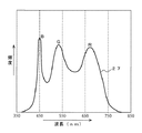
[第1の実施形態の出射光の波長分布説明:図6]
次に、第1の実施形態の半導体発光装置20から出射される出射光27の波長分布の一例を図6を用いて説明する。図6において、横軸は出射光の波長であり、単位はnmである。縦軸は輝度であり、相対値として示している。半導体発光装置20からの出射光27は、前述したように、青色LEDから青色光Bと、緑蛍光体によって波長変換された緑色光Gと、赤蛍光体によって波長変換された赤色光Rとが合成された光となる。ここで、青色光Bの波長は450nm付近であって、青色LEDからの出射光であるので波長分布が狭く、緑色光Gと赤色光Rの波長は、それぞれ蛍光体による変換光であるので比較的広い分布特性を有している。
[Explanation of wavelength distribution of emitted light of first embodiment: FIG. 6]
Next, an example of the wavelength distribution of the emitted light 27 emitted from the semiconductor
以上のように、第1の実施形態の半導体発光装置20は、蛍光体9aを含有する蛍光樹脂9で被覆された蛍光型LED10を用いることで、含有する蛍光体を蛍光型LEDごとに個別に変えることが出来る。このため、LED素子を青色LEDとして、この青色LEDからの青色光Bによって励起する緑蛍光体と赤蛍光体を個別に含有した蛍光型LEDを用いることで、図6に示すように、青色光B、緑色光G、赤色光Rがそれぞれバランスよく出射される半導体発光装置を実現することができる。
As described above, the semiconductor
この結果、演色性に優れた真の白色光に近い出射光を出射する高性能の半導体発光装置を提供できる。また、緑蛍光体を有する蛍光型LED10と赤蛍光体を有する蛍光型LED10の個数の比率を変えることで、出射光の発光色を用途に応じて任意に調整することも可能である。
As a result, it is possible to provide a high-performance semiconductor light emitting device that emits emitted light close to true white light with excellent color rendering. Further, by changing the ratio of the number of
また、蛍光型LED10の隣同士の電極を向き合わせて直接接続することで、上層下層の2層で構成されるので、実装密度を高くすることが可能であり、小型で高輝度高出力の半導体発光装置を実現できる。また、下層側の蛍光型LED10Lは、金属板21に密着しているので、熱抵抗を極めて小さくできる。また、上層側の蛍光型LED10Uは、下層側の蛍光型LED10Lとワイヤー等を介さずに直接接続しているので、上層側の蛍光型LED10Uも同様に熱抵抗を小さくできる。これにより、広い温度範囲で使用できる放熱特性が優れた発光装置を提供できる。なお、上層側の蛍光型LED10Uと下層側の蛍光型LED10Lに含有する蛍光体は、緑や赤に限定されるものではない。
In addition, since the electrodes adjacent to each other of the
[第1の実施形態の変形例の説明:図7]
次に、第1の実施形態の変形例を図7を用いて説明する。この変形例の基本的な構成は第1の実施形態と同様であり、蛍光型LED10のLED素子4の種類と蛍光樹脂9に含有する蛍光体9aの種類のみが異なっているので、構成の説明は省略し、出射光の波長分布の違いを中心に説明する。
[Description of Modification of First Embodiment: FIG. 7]
Next, a modification of the first embodiment will be described with reference to FIG. The basic configuration of this modification is the same as that of the first embodiment, and only the type of the
ここで、第1の実施形態の変形例は、蛍光型LED10のLED素子4が近紫外線LEDで構成され、蛍光型LED10を被覆する蛍光樹脂9(図1参照)の蛍光体9aは、青蛍光体、緑蛍光体、赤蛍光体がそれぞれ個別に含有する構成である。たとえば、上層側の蛍光型LED10Uに青蛍光体と緑蛍光体を個別に含有させ、下層側の蛍光型LED10Lに赤蛍光体を含有させる構成とする。
Here, in a modification of the first embodiment, the
図7は、第1の実施形態の変形例の半導体発光装置からの出射光28の波長分布の一例を示している。図7において、横軸は出射光の波長であり、縦軸は輝度であり、相対値として示している。この変形例の半導体発光装置からの出射光28は、近紫外線LEDからの近紫外光nUVと、青蛍光体によって波長変換された青色光Bと、緑蛍光体によって波長変換された緑色光Gと、赤蛍光体によって波長変換された赤色光Rとが、合成された光となる。 FIG. 7 shows an example of the wavelength distribution of the emitted light 28 from the semiconductor light emitting device according to the modification of the first embodiment. In FIG. 7, the horizontal axis represents the wavelength of the emitted light, and the vertical axis represents the luminance, which is shown as a relative value. Outgoing light 28 from the semiconductor light emitting device of this modification includes near ultraviolet light nUV from a near ultraviolet LED, blue light B wavelength-converted by a blue phosphor, and green light G wavelength-converted by a green phosphor. The red light R that has been wavelength-converted by the red phosphor becomes a synthesized light.
ここで、変形例の波長分布は第1の実施形態の波長分布(図6参照)と異なり、青色光Bも蛍光体による変換光であるので比較的広い分布特性を有している。なお、400nm付近の小さな波長のピークは、近紫外線LEDからの近紫外光nUVであり、この近紫外光nUVが励起光となって、それぞれの蛍光体を励起するのである。 Here, the wavelength distribution of the modification is different from the wavelength distribution of the first embodiment (see FIG. 6), and the blue light B is also converted light by the phosphor, and thus has a relatively wide distribution characteristic. Note that the peak of a small wavelength near 400 nm is near-ultraviolet light nUV from a near-ultraviolet LED, and this near-ultraviolet light nUV becomes excitation light to excite each phosphor.
以上のように、第1の実施形態の変形例は、青色光B、緑色光G、赤色光Rのすべてを、蛍光体をそれぞれ個別に含有した蛍光型LEDによって得ているので、LED集合体を構成するそれぞれの蛍光型LED10の個数の比率を選択することで、用途に応じて出射光の色合いを幅広く調整できる半導体発光装置を提供することができる。たとえば、赤蛍光体を含有する蛍光型LEDの数を増やせば、赤味を増した暖かみのある出射光を得ることができ、また、青蛍光体を含有する蛍光型LEDの数を増やせば、青味を増したクールな雰囲気の出射光を得ることができる。
As described above, in the modified example of the first embodiment, all of the blue light B, the green light G, and the red light R are obtained by the fluorescent LEDs that individually contain the phosphors. By selecting the ratio of the number of the
[第2の実施形態の半導体発光装置の動作説明:図8]
次に、第2の実施形態の半導体発光装置を図8を用いて説明する。この第2の実施形態は、第1の実施形態と基本的な構成が同じであり、蛍光型LED10の蛍光樹脂9に含有する蛍光体9aの種類と、LED集合体を封止する封止材26の含有物のみが異なるので、同一要素には同一番号を付して重複する構成の説明は省略し、第2の実施形態の動作と、出射光の波長分布を中心に説明する。ここで、第2の実施形態は、蛍光型LED10のLED素子4は第1の実施形態と同様に青色LEDであり、蛍光型LED10の外周面を被覆する蛍光樹脂9に含有される蛍光体9a(図1参照)はYAG蛍光体であり、封止材26には赤蛍光体が含有されている。
[Description of Operation of Semiconductor Light Emitting Device of Second Embodiment: FIG. 8]
Next, the semiconductor light emitting device of the second embodiment will be described with reference to FIG. This second embodiment has the same basic configuration as the first embodiment, and the type of phosphor 9a contained in the
図8は第1の実施形態の側面図(図2(b)参照)と同様な側面図であり、説明をわかりやすくするために縦の比率を大きくして示している。図8において、符号40は第2の実施形態の半導体発光装置である。半導体発光装置40の発光エリア22bに露出する金属板21の表面には、蛍光型LED10で構成されるLED集合体30、31、32が密着して配置され、個々の蛍光型LED10は、図示しないが青色LEDで構成され、被覆する蛍光樹脂9(ここでは図示せず)には、前述したように、YAG蛍光体が含有されている。また、すべてのLED集合体30、31、32は、封止材26によって封止され、この封止材26には、前述したように、赤蛍光体41(黒丸で示す)が略均一に含有されている。
FIG. 8 is a side view similar to the side view of the first embodiment (see FIG. 2B), and the vertical ratio is enlarged for easy understanding. In FIG. 8,
ここで、半導体発光装置40に外部から所定の駆動電圧Vdが供給されると、LED集合体30、31、32を構成する個々の蛍光型LED10が動作して、青色LEDから青色光Bが出射される。この青色光Bの一部が、蛍光樹脂9に含有されるYAG蛍光体(図示せず)に吸収されると、YAG蛍光体が励起して黄色光Yを出射する。また、青色光Bの一部が封止材26に含有される赤蛍光体41に吸収されると、赤蛍光体41が励起して赤色光Rを出射する。以上の動作によって、半導体発光装置40から青色光B、黄色光Y、赤色光Rが合成された出射光42が出射される。なお、実際の出射光42は、青色光B、黄色光Y、赤色光Rがほぼ均一に混ざり合った合成光となる。
Here, when a predetermined drive voltage Vd is supplied to the semiconductor
[第2の実施形態の出射光の波長分布説明:図9]
次に、第2の実施形態の半導体発光装置40から出射される出射光42の波長分布の一例を図9を用いて説明する。図9において、横軸は出射光42の波長であり、単位はnmである。縦軸は輝度であり、相対値として示している。半導体発光装置40からの出射光42は、前述したように、青色LEDからの青色光Bと、YAG蛍光体によって波長変換された黄色光Yと、赤蛍光体41によって波長変換された赤色光Rとが、合成された光となる。ここで、青色光Bの波長は第1の実施形態と同様に450nm付近であり、青色LEDからの出射光であるので波長分布が狭く、黄色光Yと赤色光Rの波長は、蛍光体による変換光であるので比較的広い分布特性を有している。
[Explanation of wavelength distribution of emitted light of second embodiment: FIG. 9]
Next, an example of the wavelength distribution of the emitted light 42 emitted from the semiconductor
ここで、青色LEDからの青色光BとYAG蛍光体による黄色光Yが合成されると、擬似白色光となるが、この第2の実施形態では、封止材26に赤蛍光体41を含有させたことで、赤色光Rが加えられることになる。これにより、擬似白色光に赤味が加えられた温かみのある出射光を得ることができる。この第2の実施形態は、2種類の蛍光型LEDが必要である第1の実施形態と比較して、蛍光型LED10の種類がYAG蛍光体を含有した1種類のみの構成なので、製造工程を簡素化できる特徴を備えている。
Here, when the blue light B from the blue LED and the yellow light Y by the YAG phosphor are combined, pseudo white light is obtained. In the second embodiment, the sealing material 26 contains the red phosphor 41. As a result, red light R is added. Thereby, warm outgoing light in which redness is added to pseudo white light can be obtained. Compared with the first embodiment, which requires two types of fluorescent LEDs, the second embodiment has only one type of
また、第1の実施形態と同様に、蛍光型LED10は上層下層の2層で構成されるので、実装密度を高くすることが可能であり、小型で高輝度高出力の半導体発光装置を実現できる。また、下層側の蛍光型LEDは、金属板21に密着しているので、熱抵抗を極めて小さくでき、上層側の蛍光型LEDも下層側の蛍光型LEDと直接接続しているので熱抵抗が小さく、これにより、放熱特性に優れた半導体発光装置を提供できる。
Similarly to the first embodiment, since the
[第2の実施形態の変形例の説明:図10]
次に、第2の実施形態の変形例を図10を用いて説明する。この変形例の基本的な構成は第2の実施形態と同様であり、蛍光型LED10を被覆する蛍光樹脂9に含有する蛍光体9aの種類と、LED集合体を封止する封止材26に含有する蛍光体の種類のみが異なるので、構成と動作の説明は省略し、出射光の波長分布の違いを中心に説明する。ここで、第2の実施形態の変形例は、蛍光型LED10のLED素子4が青色LEDで構成され、蛍光型LED10を被覆する蛍光樹脂9に含有される蛍光体9a(図1参照)は、第1の実施形態と同様に緑蛍光体と赤蛍光体であり、また、封止材26にはYAG蛍光体が含有される構成である。
[Description of Modification of Second Embodiment: FIG. 10]
Next, a modification of the second embodiment will be described with reference to FIG. The basic configuration of this modification is the same as that of the second embodiment. The type of the phosphor 9a contained in the
なお、蛍光樹脂9の蛍光体9aは、第1の実施形態と同様に、上層側の蛍光型LED10Uの蛍光樹脂9には緑蛍光体が含有され、下層側の蛍光型LED10Lの蛍光樹脂9には赤蛍光体が含有される。
As in the first embodiment, the fluorescent resin 9a of the
図10は、第2の実施形態の変形例の半導体発光装置からの出射光43の波長分布の一例を示している。図10において、横軸は出射光の波長であり、縦軸は輝度であり、相対値として示している。この変形例の半導体発光装置からの出射光43は、青色LEDからの青色光Bと、緑蛍光体によって波長変換された緑色光Gと、赤蛍光体によって波長変換された赤色光Rと、封止材26に含有されるYAG蛍光体からの黄色光Yが合成された光となる。 FIG. 10 shows an example of the wavelength distribution of the emitted light 43 from the semiconductor light emitting device according to the modification of the second embodiment. In FIG. 10, the horizontal axis represents the wavelength of outgoing light, and the vertical axis represents luminance, which is shown as a relative value. The emitted light 43 from the semiconductor light emitting device of this modification includes blue light B from a blue LED, green light G that has been wavelength-converted by a green phosphor, red light R that has been wavelength-converted by a red phosphor, and sealing. The yellow light Y from the YAG phosphor contained in the stop material 26 is synthesized light.
すなわち、第2の実施形態による出射光42の波長分布(図9参照)と比較して、第2の実施形態の変形例の出射光43は、緑蛍光体による緑色光Gが追加されることになり、演色性に優れた真の白色光に近い出射光が得られる高性能な半導体発光装置を提供することができる。 That is, as compared with the wavelength distribution of the emitted light 42 according to the second embodiment (see FIG. 9), the emitted light 43 of the modified example of the second embodiment is added with the green light G by the green phosphor. Thus, it is possible to provide a high-performance semiconductor light-emitting device capable of obtaining emitted light close to true white light with excellent color rendering properties.
[第3の実施形態の構成説明:図11]
次に、第3の実施形態の半導体発光装置を図11を用いて説明する。図11において、符号50は第3の実施形態の半導体発光装置である。半導体発光装置50は、電球型の筐体を備えており、LED集合体を封止する略球形の樹脂カバー51、絶縁材で成る支持部52、および、外部からの電力を入力するための接続部53を有している。支持部52の略中央には絶縁基板で成る電極部54が配置され、この電極部54には一対の電極54a、54bが形成されている。
[Configuration of Third Embodiment: FIG. 11]
Next, the semiconductor light emitting device of the third embodiment will be described with reference to FIG. In FIG. 11,
この電極部54の図面上の上部には、蛍光型LED10が略コ形に直列接続されたLED集合体55が配置されている。ここで、電極部54は支持部52に対して垂直に取り付けられているので、LED集合体55も電極部54に沿って垂直方向に支持されている。
An
また、支持部52の内部には、LED集合体55を駆動する駆動部56(破線で示す)を有している。ここで、LED集合体55の両端部に位置する一対の蛍光型LED10は、電極部54の電極54a、54bに接続され、電極54a、54bは図示しない手段によって駆動部56に接続され、駆動部56は接続部53の接続端子53a、53bに接続されている。この構成によって、接続部53に外部から、たとえばAC100Vが供給されると、駆動部56はAC100Vを所定の直流電圧に変換し、電極部54を介してLED集合体55に直流の駆動電圧を供給してLED集合体55を点灯する。
Further, inside the support portion 52, there is a drive portion 56 (shown by a broken line) that drives the
なお、接続部53の形状は、一般的な白熱電球のねじ込み式(E26口金等)に等しい構造にすることによって、半導体発光装置50は白熱電球に置き換えることができる。また、樹脂カバー51は、透明でも半透明でもよく、樹脂に反射材を含有させてもよく、または、樹脂に所定の蛍光体を含有させてもよい。
Note that the semiconductor
[第3の実施形態のLED集合体の構成説明:図12]
次に、第3の実施形態の半導体発光装置50に組み込まれる略コ形のLED集合体55の構成を図12を用いて説明する。図12において、LED集合体55は、蛍光型LED10の集合体であり、前述したように、略コ形に直列接続されている。ここで、各蛍光型LED10は、図1で示した蛍光型LED10と同一であり、第1および第2の実施形態と同様に、LED集合体55を構成する蛍光型LED10は、隣接する蛍光型LED10と互いに向き合い、外部接続電極7、8(図1参照)が直接半田等によって電気的に接続される。そして、接続方向は図示するように、略コ形の直線部分は直線方向に接続され、略コ形の角部は直角方向に接続される。
[Configuration Description of LED Assembly of Third Embodiment: FIG. 12]
Next, the configuration of the substantially
そして、LED集合体55の両端部に位置する一対の蛍光型LED10a、10bが電極部54の電極54a、54bにそれぞれ接続され、電極54a、54bに所定の駆動電圧が供給されることで、LED集合体55に駆動電流が流れて、個々の蛍光形LED10が点灯する。ここで、第1の実施形態と同様に、蛍光形LED10に青色LEDを用い、蛍光型LED10を被覆する蛍光樹脂9(図1参照)に緑蛍光体と赤蛍光体を個別に含有させるならば、第1の実施形態と同様な波長分布(図6参照)の出射光を得ることができ、青色光B、緑色光G、赤色光Rがそれぞれバランスよく出射される演色性に優れた半導体発光装置を実現することができる。
Then, the pair of fluorescent LEDs 10a and 10b located at both ends of the
また、第2の実施形態と同様に、蛍光形LED10に青色LEDを用い、蛍光型LED10を被覆する蛍光樹脂9にYAG蛍光体を含有させ、樹脂カバー51に赤蛍光体を含有させるならば、第2の実施形態と同様な波長分布(図9参照)の出射光を得ることができる。また、略コ形のLED集合体55は、前述したように、支持部52に対して垂直に支持されているので、発光形状(光源形状)や発光の広がりがフィラメント型電球に近似したものとなり、本実施形態は、フィラメント型電球と同等の発光特性を有する半導体発光装置を提供することができる。
Similarly to the second embodiment, if a blue LED is used for the
以上のように、第3の実施形態の半導体発光装置50は、蛍光型LED10を略コ形に直列接続した集合体として装置内部に組み込むので、フィラメント型電球の置き換え用として好適な省エネ型半導体発光装置を実現できる。また、蛍光型LED10を用いることによって、様々な蛍光体を含有する蛍光樹脂9を任意に選択できるので、多様な発光色を備えた電球型発光装置を簡単に製造することができる。
As described above, the semiconductor
尚、本発明の実施例で示した各図面等は、これに限定されるものではなく、本発明の要旨を満たすものであれば、任意に変更してよい。 It should be noted that the drawings shown in the embodiments of the present invention are not limited to this, and may be arbitrarily changed as long as they satisfy the gist of the present invention.
本発明の半導体発光装置は、優れた演色性と小型で高輝度高出力の発光装置を実現できるので、様々な照明用光源や車載用光源などに幅広く利用することが出来る。 Since the semiconductor light emitting device of the present invention can realize a light emitting device with excellent color rendering properties and a small size with high luminance and high output, it can be widely used for various illumination light sources and in-vehicle light sources.
1 透明基板
2 n型窒化物半導体層
3 p型窒化物半導体層
4 半導体発光素子(LED素子)
6 絶縁層
7、8 外部接続電極
9 蛍光樹脂
9a 蛍光体
10、101、102、103、104、・・・117、10a、10b 蛍光型半導体発光素子(蛍光型LED)
20、40、50 半導体発光装置
21 金属板
22 絶縁基板
22a 貫通孔
22b 発光エリア
23、24 導電パターン
25 封止枠
26 封止材
27、28、42、43 出射光
30、31、32、55 発光素子集合体(LED集合体)
41 赤蛍光体
51 樹脂カバー
52 支持部
53 接続部
54 電極部
56 駆動部
R 赤色光
G 緑色光
B 青色光
Y 黄色光
DESCRIPTION OF
6 Insulating
20, 40, 50 Semiconductor
41 Red phosphor 51 Resin cover 52 Support part 53
Claims (10)
少なくとも前記外部接続電極以外の外周面を蛍光体を含有する樹脂で被覆した蛍光型半導体発光素子を備え、
該蛍光型半導体発光素子の前記外部接続電極同士を電気的接続手段を介して接続することで複数の前記蛍光型半導体発光素子を直列接続して発光素子集合体を構成し、
前記発光素子集合体は、前記蛍光型半導体発光素子の隣同士の前記外部接続電極を向き合わせて接続することで、前記蛍光型半導体発光素子の隣同士が厚み方向で重なり上層下層となるように構成し、
前記発光素子集合体は、前記蛍光型半導体発光素子の隣同士を直線方向または直角方向に接続して所定の発光エリアを分担するように構成することを特徴とする半導体発光装置。 an external connection electrode connected to each of the n-type semiconductor layer and the p-type semiconductor layer;
A fluorescent semiconductor light emitting device having at least an outer peripheral surface other than the external connection electrode coated with a resin containing a phosphor,
A plurality of the fluorescent semiconductor light emitting elements are connected in series by connecting the external connection electrodes of the fluorescent semiconductor light emitting elements through electrical connection means to form a light emitting element assembly ,
The light emitting element assembly is formed by connecting the external connection electrodes adjacent to the fluorescent semiconductor light emitting element facing each other so that the fluorescent semiconductor light emitting elements are adjacent to each other in the thickness direction and become an upper layer and a lower layer. Configure
The light emitting element assembly is configured to share a predetermined light emitting area by connecting the fluorescent semiconductor light emitting elements adjacent to each other in a straight line direction or a right angle direction .
Priority Applications (2)
| Application Number | Priority Date | Filing Date | Title |
|---|---|---|---|
| JP2013206057A JP6301097B2 (en) | 2013-10-01 | 2013-10-01 | Semiconductor light emitting device |
| US14/499,174 US9559083B2 (en) | 2013-10-01 | 2014-09-27 | Semiconductor light-emitting device |
Applications Claiming Priority (1)
| Application Number | Priority Date | Filing Date | Title |
|---|---|---|---|
| JP2013206057A JP6301097B2 (en) | 2013-10-01 | 2013-10-01 | Semiconductor light emitting device |
Publications (2)
| Publication Number | Publication Date |
|---|---|
| JP2015070242A JP2015070242A (en) | 2015-04-13 |
| JP6301097B2 true JP6301097B2 (en) | 2018-03-28 |
Family
ID=52836609
Family Applications (1)
| Application Number | Title | Priority Date | Filing Date |
|---|---|---|---|
| JP2013206057A Active JP6301097B2 (en) | 2013-10-01 | 2013-10-01 | Semiconductor light emitting device |
Country Status (2)
| Country | Link |
|---|---|
| US (1) | US9559083B2 (en) |
| JP (1) | JP6301097B2 (en) |
Families Citing this family (6)
| Publication number | Priority date | Publication date | Assignee | Title |
|---|---|---|---|---|
| USD774474S1 (en) * | 2015-02-04 | 2016-12-20 | Xiaofeng Li | Light emitting diodes on a printed circuit board |
| KR20170026801A (en) | 2015-08-28 | 2017-03-09 | 삼성전자주식회사 | Semiconductor light emitting device package and light source module using the same |
| JP6611036B2 (en) * | 2015-09-10 | 2019-11-27 | パナソニックIpマネジメント株式会社 | Light emitting device and light source for illumination |
| FR3063129B1 (en) * | 2017-02-17 | 2019-04-12 | Valeo Vision | LIGHT MODULE WITH REDUCED DIMENSIONS |
| KR101980548B1 (en) * | 2017-11-09 | 2019-05-21 | 엘지전자 주식회사 | Lamp for vehicle and vehicle |
| JP2020053568A (en) * | 2018-09-27 | 2020-04-02 | 日亜化学工業株式会社 | Light-emitting device and manufacturing method thereof |
Family Cites Families (29)
| Publication number | Priority date | Publication date | Assignee | Title |
|---|---|---|---|---|
| JP3571477B2 (en) | 1996-12-06 | 2004-09-29 | ローム株式会社 | Semiconductor light emitting device |
| JP4081985B2 (en) * | 2001-03-02 | 2008-04-30 | 日亜化学工業株式会社 | Light emitting device and manufacturing method thereof |
| US20050073846A1 (en) * | 2001-09-27 | 2005-04-07 | Kenji Takine | Lightemitting device and method of manufacturing the same |
| US6841802B2 (en) * | 2002-06-26 | 2005-01-11 | Oriol, Inc. | Thin film light emitting diode |
| JP3813599B2 (en) * | 2003-06-13 | 2006-08-23 | ローム株式会社 | Method for manufacturing white light emitting diode element |
| JP2006126106A (en) * | 2004-11-01 | 2006-05-18 | Tokai Corp | Method of detecting remaining amount of liquid |
| JP2006244725A (en) * | 2005-02-28 | 2006-09-14 | Atex Co Ltd | Led lighting system |
| WO2006098450A1 (en) * | 2005-03-18 | 2006-09-21 | Mitsubishi Chemical Corporation | Light-emitting device, white light-emitting device, illuminator, and image display |
| JP2007115928A (en) | 2005-10-20 | 2007-05-10 | Citizen Electronics Co Ltd | Semiconductor light-emitting device |
| JP4600455B2 (en) * | 2006-11-30 | 2010-12-15 | 東芝ライテック株式会社 | Lighting device |
| TW200845423A (en) * | 2006-12-04 | 2008-11-16 | Alps Electric Co Ltd | Light emitting device and projector |
| JP5032171B2 (en) * | 2007-03-26 | 2012-09-26 | 株式会社東芝 | Semiconductor light emitting device, method for manufacturing the same, and light emitting device |
| JP4938611B2 (en) * | 2007-10-09 | 2012-05-23 | アルプス電気株式会社 | Semiconductor light emitting device |
| US20090140279A1 (en) * | 2007-12-03 | 2009-06-04 | Goldeneye, Inc. | Substrate-free light emitting diode chip |
| US8461613B2 (en) * | 2008-05-27 | 2013-06-11 | Interlight Optotech Corporation | Light emitting device |
| JP5294902B2 (en) * | 2009-01-27 | 2013-09-18 | シチズン電子株式会社 | Manufacturing method of surface mounted light emitting device |
| JP2011151268A (en) * | 2010-01-22 | 2011-08-04 | Sharp Corp | Light-emitting device |
| JP2011165833A (en) * | 2010-02-08 | 2011-08-25 | Toshiba Corp | Led module |
| KR101543333B1 (en) * | 2010-04-23 | 2015-08-11 | 삼성전자주식회사 | Lead frame for light emitting device package, light emitting device package, and illumination apparatus employing the light emitting device package |
| JP2012004519A (en) * | 2010-05-17 | 2012-01-05 | Sharp Corp | Light emitting device and illumination device |
| US8714762B2 (en) * | 2011-05-03 | 2014-05-06 | Zhou Cai | LED light source and manufacturing method thereof |
| CN107087343B (en) * | 2011-05-27 | 2019-04-19 | 夏普株式会社 | Light emitting device and lighting device |
| JP5833850B2 (en) * | 2011-07-08 | 2015-12-16 | シチズン電子株式会社 | Semiconductor light emitting device and manufacturing method thereof |
| JP2013098427A (en) * | 2011-11-02 | 2013-05-20 | Citizen Electronics Co Ltd | Semiconductor light-emitting device |
| JP5883270B2 (en) * | 2011-11-02 | 2016-03-09 | シチズン電子株式会社 | LED lamp |
| JP2013106550A (en) * | 2011-11-18 | 2013-06-06 | Sharp Corp | Lighting device for growing plant |
| JP2013118292A (en) * | 2011-12-02 | 2013-06-13 | Citizen Electronics Co Ltd | Led light-emitting device |
| JP2013135082A (en) * | 2011-12-26 | 2013-07-08 | Toyoda Gosei Co Ltd | Light-emitting device |
| JP5609925B2 (en) * | 2012-07-09 | 2014-10-22 | 日亜化学工業株式会社 | Light emitting device |
-
2013
- 2013-10-01 JP JP2013206057A patent/JP6301097B2/en active Active
-
2014
- 2014-09-27 US US14/499,174 patent/US9559083B2/en not_active Expired - Fee Related
Also Published As
| Publication number | Publication date |
|---|---|
| US20150129907A1 (en) | 2015-05-14 |
| JP2015070242A (en) | 2015-04-13 |
| US9559083B2 (en) | 2017-01-31 |
Similar Documents
| Publication | Publication Date | Title |
|---|---|---|
| JP6616065B2 (en) | Light emitting module and lighting device related thereto | |
| JP6301097B2 (en) | Semiconductor light emitting device | |
| JP5345178B2 (en) | Light emitting element | |
| US7989840B2 (en) | Illumination apparatus having a plurality of semiconductor light-emitting devices | |
| US8820950B2 (en) | Light emitting device and illumination apparatus | |
| JP4338768B1 (en) | Light emitting device | |
| TWI434442B (en) | Light emitting diode package | |
| JP5499325B2 (en) | Light emitting module and lighting device | |
| US8390021B2 (en) | Semiconductor light-emitting device, light-emitting module, and illumination device | |
| US20110089815A1 (en) | Light-emitting device | |
| EP2672513B1 (en) | Multichip package structure for generating a symmetrical and uniform light-blending source | |
| JP2009065137A (en) | Light-emitting device | |
| JP2011216868A (en) | Light emitting device, and illumination apparatus | |
| JP6083253B2 (en) | Stack of light emitting devices | |
| JP5993497B2 (en) | LED lighting device | |
| KR20140036670A (en) | Light emitting device package and head light for vehicle having the same | |
| JP2009111273A (en) | Light-emitting device | |
| WO2013153938A1 (en) | Optical semiconductor light source and lighting apparatus for vehicle | |
| JP2007288138A (en) | Light emitting device | |
| JP2008218998A (en) | Light emitting device | |
| US9443832B2 (en) | Light emitting device, light source for illumination, and illumination apparatus | |
| JP2018129492A (en) | Light-emitting device, and illuminating device | |
| JP2008244468A (en) | Light-emitting device | |
| JP2008244469A (en) | Light-emitting device | |
| WO2015072120A1 (en) | Light emitting device, light emitting module, lighting device and lamp |
Legal Events
| Date | Code | Title | Description |
|---|---|---|---|
| RD03 | Notification of appointment of power of attorney |
Free format text: JAPANESE INTERMEDIATE CODE: A7423 Effective date: 20150202 |
|
| A621 | Written request for application examination |
Free format text: JAPANESE INTERMEDIATE CODE: A621 Effective date: 20160923 |
|
| A977 | Report on retrieval |
Free format text: JAPANESE INTERMEDIATE CODE: A971007 Effective date: 20170721 |
|
| A131 | Notification of reasons for refusal |
Free format text: JAPANESE INTERMEDIATE CODE: A131 Effective date: 20170808 |
|
| A521 | Request for written amendment filed |
Free format text: JAPANESE INTERMEDIATE CODE: A523 Effective date: 20171006 |
|
| TRDD | Decision of grant or rejection written | ||
| A01 | Written decision to grant a patent or to grant a registration (utility model) |
Free format text: JAPANESE INTERMEDIATE CODE: A01 Effective date: 20180206 |
|
| A61 | First payment of annual fees (during grant procedure) |
Free format text: JAPANESE INTERMEDIATE CODE: A61 Effective date: 20180228 |
|
| R150 | Certificate of patent or registration of utility model |
Ref document number: 6301097 Country of ref document: JP Free format text: JAPANESE INTERMEDIATE CODE: R150 |
|
| R250 | Receipt of annual fees |
Free format text: JAPANESE INTERMEDIATE CODE: R250 |
|
| R250 | Receipt of annual fees |
Free format text: JAPANESE INTERMEDIATE CODE: R250 |