JP6300610B2 - LED power supply device and LED lighting device - Google Patents

LED power supply device and LED lighting device Download PDF

Info

Publication number
JP6300610B2
JP6300610B2 JP2014077552A JP2014077552A JP6300610B2 JP 6300610 B2 JP6300610 B2 JP 6300610B2 JP 2014077552 A JP2014077552 A JP 2014077552A JP 2014077552 A JP2014077552 A JP 2014077552A JP 6300610 B2 JP6300610 B2 JP 6300610B2
Authority
JP
Japan
Prior art keywords
power supply
voltage
led
supply device
input
Prior art date
Legal status (The legal status is an assumption and is not a legal conclusion. Google has not performed a legal analysis and makes no representation as to the accuracy of the status listed.)
Active
Application number
JP2014077552A
Other languages
Japanese (ja)
Other versions
JP2015201255A (en
Inventor
稔 松本
稔 松本
賢仁 司城
賢仁 司城
Current Assignee (The listed assignees may be inaccurate. Google has not performed a legal analysis and makes no representation or warranty as to the accuracy of the list.)
Eye Lighting Systems Corp
Original Assignee
Eye Lighting Systems Corp
Priority date (The priority date is an assumption and is not a legal conclusion. Google has not performed a legal analysis and makes no representation as to the accuracy of the date listed.)
Filing date
Publication date
Application filed by Eye Lighting Systems Corp filed Critical Eye Lighting Systems Corp
Priority to JP2014077552A priority Critical patent/JP6300610B2/en
Publication of JP2015201255A publication Critical patent/JP2015201255A/en
Application granted granted Critical
Publication of JP6300610B2 publication Critical patent/JP6300610B2/en
Active legal-status Critical Current
Anticipated expiration legal-status Critical

Links

Images

Description

本発明はLED電源装置及びそれを用いたLED照明装置に関する。   The present invention relates to an LED power supply device and an LED lighting device using the LED power supply device.

特許文献1は、消灯状態から点灯状態に切り替わる際に発生する閃光を低減するLED点灯装置を開示する。そのLED点灯装置は、LEDに駆動電流を供給する絶縁型フライバックコンバータと、検出されたLEDの順方向電流が目標値となるようにスイッチング動作を制御する制御回路部を備える。制御回路部は、消灯状態のLEDを点灯させるために絶縁型フライバックコンバータのスイッチング動作を開始させた時点からLEDへの印加電圧が点灯開始電圧に増加するまでの間に、スイッチング素子のオン時間が長い第1のスイッチング期間を設けた後、オン時間が短い第2のスイッチング期間を設ける。   Patent Document 1 discloses an LED lighting device that reduces flash light generated when switching from a light-off state to a light-on state. The LED lighting device includes an isolated flyback converter that supplies a drive current to the LED, and a control circuit unit that controls the switching operation so that the detected forward current of the LED becomes a target value. The control circuit unit switches the on-time of the switching element from the time when the switching operation of the isolated flyback converter is started to turn on the off-state LED until the voltage applied to the LED increases to the lighting start voltage. After providing the first switching period having a longer period, a second switching period having a shorter on-time is provided.

特開2013−69766号公報JP 2013-69766 A

ところで、特許文献1のようなフライバックコンバータ等のスイッチング電源回路を用いるLED電源装置においては、点灯開始だけでなく消灯時にも閃光が発生し得る。これは、入力電源がオフされた時に、フライバックコンバータの一次側の平滑コンデンサに充電電圧が残った状態で制御回路の制御電圧が低下し、二次側の出力制御が効かなくなることに起因する。これにより、例えば、消灯直前にスイッチング電源回路が最大出力状態となり、平滑コンデンサの電荷が二次側のLEDにおいて一気に放電されて閃光が発生する。しかし、このようなLED消灯時の閃光は、点灯開始時の閃光とは異なり、照明を消して暗くするというユーザの意図に反する現象であり、ユーザにおける視覚的違和感は点灯開始時の閃光よりも大きいものとなる。またさらに、消灯前の閃光によりユーザの目に与えられた残光により、ユーザの目が消灯後の暗さに適応するのに時間がかかり、不快感がもたらされる。このように、消灯直前の閃光によってユーザには視覚的違和感、不快感等がもたらされてしまう。   By the way, in an LED power supply device using a switching power supply circuit such as a flyback converter as in Patent Document 1, a flash can be generated not only at the start of lighting but also at the time of turning off. This is because when the input power is turned off, the control voltage of the control circuit is lowered while the charging voltage remains in the smoothing capacitor on the primary side of the flyback converter, and the output control on the secondary side becomes ineffective. . Thereby, for example, the switching power supply circuit is in a maximum output state immediately before the light is turned off, and the electric charge of the smoothing capacitor is discharged at once in the secondary side LED, and flashing is generated. However, unlike the flash at the start of lighting, such a flash when the LED is turned off is a phenomenon contrary to the user's intention to turn off the light and darken, and the visual discomfort to the user is more than the flash at the start of lighting. It will be big. Furthermore, due to the afterglow applied to the user's eyes by the flash before turning off, it takes time for the user's eyes to adapt to the darkness after turning off, resulting in discomfort. In this way, the user's visual discomfort, discomfort, and the like are brought about by the flash just before turning off.

そこで、本発明は、一次側に平滑コンデンサを有するDC/DCコンバータを備えるLED電源装置において、LED消灯直前の閃光を防止する構成を提供することを課題とする。   Therefore, an object of the present invention is to provide a configuration for preventing flashing immediately before the LED is turned off in an LED power supply device including a DC / DC converter having a smoothing capacitor on the primary side.

本発明のLED電源装置は、交流入力電圧を直流変換して平滑コンデンサを充電するAC/DC変換部と、一次側のスイッチング素子のスイッチング動作によって平滑コンデンサの電圧を変圧して、変圧された第1の二次出力をLEDに供給するDC/DCコンバータと、交流入力電圧を検出する入力電源検出部と、DC/DCコンバータの第2の二次出力が給電されてスイッチング素子を駆動するように構成され、交流入力電圧の停止が検出された場合に、第2の二次出力に対する第1の二次出力の割合を低減するようにスイッチング素子の駆動を制御する制御部を備える。   The LED power supply apparatus of the present invention transforms the voltage of the smoothing capacitor by transforming the voltage of the smoothing capacitor by the AC / DC conversion unit that converts the AC input voltage to DC and charges the smoothing capacitor, and the switching operation of the primary side switching element. A DC / DC converter that supplies the secondary output of 1 to the LED, an input power source detection unit that detects an AC input voltage, and a second secondary output of the DC / DC converter is fed to drive the switching element. A controller configured to control driving of the switching element so as to reduce a ratio of the first secondary output to the second secondary output when the stop of the AC input voltage is detected.

本発明のLED電源装置によると、入力電源検出部及び制御部によって交流入力電圧の停止が検出された場合に、制御部は、DC/DCコンバータから制御部への二次出力に対するDC/DCコンバータからLEDへの二次出力の割合を低減するようにスイッチング素子の駆動を制御する。したがって、入力電源停止後に、DC/DCコンバータの一次側の平滑コンデンサの残存エネルギーがLEDにおいて一気に放出される状態が回避され、LED消灯直前の閃光が防止される。   According to the LED power supply device of the present invention, when the stop of the AC input voltage is detected by the input power supply detection unit and the control unit, the control unit is a DC / DC converter for the secondary output from the DC / DC converter to the control unit. The driving of the switching element is controlled so as to reduce the ratio of the secondary output from the LED to the LED. Therefore, after the input power is stopped, a state in which the residual energy of the smoothing capacitor on the primary side of the DC / DC converter is released at once in the LED is avoided, and flashing immediately before the LED is turned off is prevented.

ここで、制御部は、交流入力電圧の停止が検出された場合に第1の二次出力の電圧がLEDの順方向降下電圧未満となるようにスイッチング素子の駆動を制御するように構成される。これにより、通常の使用と同様に交流入力電源の停止後に消灯状態が即座に得られるとともに確実にLEDにおける閃光が防止される。   Here, the control unit is configured to control the driving of the switching element so that the voltage of the first secondary output becomes less than the forward voltage drop of the LED when the stop of the AC input voltage is detected. . As a result, as in normal use, a light-off state can be obtained immediately after the AC input power supply is stopped, and flashing in the LED is reliably prevented.

一形態として、AC/DC変換部は、交流入力電圧を整流する全波整流器と、上記平滑コンデンサを含み全波整流器の脈流出力を昇圧して平滑コンデンサに充電する力率改善回路を含み、入力電源検出部及び制御部が、脈流出力に基づいて交流入力電圧の停止を検出するように構成される。これにより、入力電源停止から数十ms程度で速やかに上記の消灯制御が開始され、高い応答性で閃光を防止することができる。   As one form, the AC / DC converter includes a full-wave rectifier that rectifies an AC input voltage, and a power factor correction circuit that includes the smoothing capacitor and boosts the pulsating output of the full-wave rectifier to charge the smoothing capacitor. An input power supply detection part and a control part are comprised so that the stop of alternating current input voltage may be detected based on a pulsating flow output. As a result, the above-described extinguishing control is started promptly within several tens of ms after the input power supply is stopped, and flashing can be prevented with high responsiveness.

また、他の形態として、入力電源検出部が、交流入力電圧を整流する整流器を備え、入力電源検出部及び制御部が整流器の脈流出力に基づいて交流入力電圧の停止を検出するように構成されるようにしてもよい。これにより、コンデンサインプット型の回路においても、入力電源停止から数十ms程度で速やかに上記の消灯制御が開始され、高い応答性で閃光を防止することができる。   As another form, the input power source detection unit includes a rectifier that rectifies the AC input voltage, and the input power source detection unit and the control unit are configured to detect the stop of the AC input voltage based on the pulsating output of the rectifier. You may be made to do. As a result, even in the capacitor input type circuit, the above-described extinguishing control is started quickly in about several tens of milliseconds after the input power supply is stopped, and flashing can be prevented with high responsiveness.

またさらに、他の形態として、入力電源検出部が、平滑コンデンサの平滑電圧を検出するように構成され、平滑電圧が所定の閾値未満となった場合に入力電源検出部及び制御部が交流入力電圧の停止を検出するように構成されるようにしてもよい。この構成によると、入力電源検出部の出力が直流となるため、制御部における制御状態の切換え構成に設計の自由度が増す。   As still another form, the input power supply detection unit is configured to detect the smoothing voltage of the smoothing capacitor, and when the smoothing voltage becomes less than a predetermined threshold, the input power supply detection unit and the control unit are connected to the AC input voltage. It may be configured to detect the stop of the. According to this configuration, since the output of the input power source detection unit is a direct current, the degree of freedom in design increases in the control state switching configuration in the control unit.

また、制御部が、外部からの調光指令信号が示す調光率に応じてスイッチング素子の駆動を制御するように構成されるとともに、調光率が所定の調光率以下の場合でかつ交流入力電圧の停止が検出された場合に第2の二次出力に対する第1の二次出力の割合を低減するように構成される。これにより、閃光のおそれがない点灯状態(例えば全光時)においては、入力電源停止後に比較的早くLED電源装置を停止させることができる。例えば、上記所定の調光率は20%に設定される。   Further, the control unit is configured to control the driving of the switching element in accordance with the dimming rate indicated by the dimming command signal from the outside, and the alternating current is when the dimming rate is equal to or less than the predetermined dimming rate. It is configured to reduce the ratio of the first secondary output to the second secondary output when a stop of the input voltage is detected. As a result, in a lighting state where there is no fear of flashing (for example, all light), the LED power supply device can be stopped relatively quickly after the input power supply is stopped. For example, the predetermined dimming rate is set to 20%.

なお、DC/DCコンバータがトランスを有する絶縁型フライバックコンバータからなり、トランスの補助巻線に制御部が接続される構成とすることが好ましい。このように、本発明のLED電源装置は、絶縁型フライバックコンバータからなるDC/DCコンバータにおいて好適に適用される。   The DC / DC converter is preferably an insulating flyback converter having a transformer, and the controller is preferably connected to the auxiliary winding of the transformer. Thus, the LED power supply device of the present invention is suitably applied to a DC / DC converter composed of an insulating flyback converter.

本発明のLED照明装置は、上記のLED電源装置と、LEDとを備える。上記効果を有するLED電源装置が採用されるので、消灯時の視覚的違和感、不快感等を解消することができるLED照明装置が実現される。   The LED lighting device of the present invention includes the above-described LED power supply device and an LED. Since the LED power supply device having the above effects is employed, an LED illumination device that can eliminate the visual discomfort and uncomfortable feeling when the lights are turned off is realized.

本発明の第1の実施形態によるLED電源装置及びLED照明装置を示す図である。It is a figure which shows the LED power supply device and LED lighting apparatus by the 1st Embodiment of this invention. 比較例によるLED電源装置の動作を説明する図である。It is a figure explaining operation | movement of the LED power supply device by a comparative example. 第1の実施形態によるLED電源装置の動作を説明する図である。It is a figure explaining operation | movement of the LED power supply device by 1st Embodiment. 第1の実施形態によるLED電源装置の動作を説明する図である。It is a figure explaining operation | movement of the LED power supply device by 1st Embodiment. 本発明の第2の実施形態によるLED電源装置及びLED照明装置を示す図である。It is a figure which shows the LED power supply device and LED lighting apparatus by the 2nd Embodiment of this invention. 第2の実施形態の一変形例における入力電源検出部を示す図である。It is a figure which shows the input power supply detection part in the modification of 2nd Embodiment. 第2の実施形態の他の変形例における入力電源検出部を示す図である。It is a figure which shows the input power supply detection part in the other modification of 2nd Embodiment. 本発明の第3の実施形態によるLED電源装置及びLED照明装置を示す図である。It is a figure which shows the LED power supply device and LED lighting apparatus by the 3rd Embodiment of this invention. 第3の実施形態によるLED電源装置の動作を説明する図である。It is a figure explaining operation | movement of the LED power supply device by 3rd Embodiment. 本発明の変形例における補助電源部の一部及び駆動制御部を説明する図である。It is a figure explaining a part of auxiliary power supply part and drive control part in the modification of this invention.

実施形態1.
図1に、本発明の第1の実施形態に係るLED電源装置1及びそれを用いたLED照明装置3の回路構成図を示す。LED照明装置3はLED電源装置1及びLED2を含む。交流電源ACからの入力電圧がLED電源装置1の入力端子T1及びT2に入力され、LED電源装置1の高電位出力端子T3及び低電位出力端子T4からの直流出力がそれぞれ配線W1及びW2を介してLEDモジュール2の端子T5及びT6に供給される。LED電源装置1の端子T7及びT8からは、外部の調光器からの調光指令信号が入力される。
Embodiment 1. FIG.
In FIG. 1, the circuit block diagram of the LED power supply device 1 which concerns on the 1st Embodiment of this invention, and the LED lighting apparatus 3 using the same is shown. The LED lighting device 3 includes an LED power supply device 1 and an LED 2. The input voltage from the AC power supply AC is input to the input terminals T1 and T2 of the LED power supply device 1, and the DC outputs from the high potential output terminal T3 and the low potential output terminal T4 of the LED power supply device 1 are respectively connected via the wirings W1 and W2. Are supplied to the terminals T5 and T6 of the LED module 2. A dimming command signal from an external dimmer is input from terminals T7 and T8 of the LED power supply device 1.

LED電源装置1は、AC/DC変換部10、DC/DCコンバータ20、駆動制御部30、出力制御部40、補助電源部50、及び入力電源検出回路60を備える。駆動制御部30、出力制御部40及び補助電源部50をまとめて制御部(30、40、50)というものとする。LED2は、端子T5と端子T6間に直列接続された複数のLED素子を含む。なお、LED電源装置1とLED2とは、1つの筐体において一体化されていてもよいし、2つの筐体において別体として構成されていてもよい。本明細書における説明において、各回路又は構成要素が上記のどのブロックに属するかは便宜的なものであり、本発明を拘束するものではない。   The LED power supply device 1 includes an AC / DC conversion unit 10, a DC / DC converter 20, a drive control unit 30, an output control unit 40, an auxiliary power supply unit 50, and an input power supply detection circuit 60. The drive control unit 30, the output control unit 40, and the auxiliary power supply unit 50 are collectively referred to as a control unit (30, 40, 50). LED2 includes a plurality of LED elements connected in series between terminal T5 and terminal T6. Note that the LED power supply device 1 and the LED 2 may be integrated in one housing, or may be configured as separate bodies in the two housings. In the description of the present specification, it is convenient for each block to which each circuit or component belongs, and the present invention is not bound thereto.

AC/DC変換部10は、全波整流器101、入力コンデンサ102、力率改善回路(以下、「PFC」という)110、及び必要に応じて全波整流器101の前段に電流ヒューズ、ノイズフィルタ等を備える。入力交流電圧が全波整流器101によって全波整流され、入力コンデンサ102に発生する脈流電圧がPFC110に供給される。PFC110は、インダクタ111、スイッチング素子112、ダイオード113、コンデンサ114(平滑コンデンサ)及びPWM制御回路115を含む。以降の説明において、コンデンサ114の負極側電極と同電位のノードを一次側グランドというものとする。   The AC / DC converter 10 includes a full-wave rectifier 101, an input capacitor 102, a power factor correction circuit (hereinafter referred to as “PFC”) 110, and, if necessary, a current fuse, a noise filter, and the like before the full-wave rectifier 101. Prepare. The input AC voltage is full-wave rectified by the full-wave rectifier 101, and the pulsating voltage generated in the input capacitor 102 is supplied to the PFC 110. The PFC 110 includes an inductor 111, a switching element 112, a diode 113, a capacitor 114 (smoothing capacitor), and a PWM control circuit 115. In the following description, a node having the same potential as the negative electrode of the capacitor 114 is referred to as a primary side ground.

スイッチング素子112はPWM制御回路115によって高周波スイッチングによりPWM制御され、これにより入力力率が改善される。スイッチング素子112がオンの期間においては、全波整流器101からの脈流電圧がインダクタ111及びスイッチング素子112に流れることによりインダクタ111にエネルギーが蓄えられる。スイッチング素子112がオフの期間においては、インダクタ111に蓄えられているエネルギーがダイオード113を介してコンデンサ114に充電される。これにより、コンデンサ114には入力電源電圧から昇圧された電圧が充電される。PWM制御回路115は、PWM制御におけるオン幅を適宜制御してスイッチング素子112をPWM駆動する。この動作によりPFC110は、昇圧された直流電圧を出力する。なお、コンデンサ114は、LED電源装置1の定格電力に応じて1μF〜1000μF程度、好ましくは10μF〜100μF程度の電解コンデンサであればよい。   The switching element 112 is PWM-controlled by high-frequency switching by the PWM control circuit 115, thereby improving the input power factor. During the period when the switching element 112 is on, energy is stored in the inductor 111 by the pulsating voltage from the full-wave rectifier 101 flowing to the inductor 111 and the switching element 112. During the period when the switching element 112 is off, the energy stored in the inductor 111 is charged to the capacitor 114 via the diode 113. As a result, the capacitor 114 is charged with a voltage boosted from the input power supply voltage. The PWM control circuit 115 drives the switching element 112 by PWM by appropriately controlling the ON width in PWM control. By this operation, the PFC 110 outputs a boosted DC voltage. The capacitor 114 may be an electrolytic capacitor of about 1 μF to 1000 μF, preferably about 10 μF to 100 μF, depending on the rated power of the LED power supply device 1.

本実施例では、DC/DCコンバータ20は絶縁型フライバックコンバータからなる。DC/DCコンバータ20は、スイッチング素子201、トランス202、ダイオード203、及びコンデンサ204を含み、必要に応じて消磁用の抵抗205及びコンデンサ206を備える。コンデンサ204は、電解コンデンサ(図示)であってもよいし、フィルムコンデンサであってもよい。コンデンサ204の負極側電極と同電位のノードを二次側グランドというものとする。DC/DCコンバータ20において、スイッチング素子201、トランス202の一次主巻線N1、抵抗205及びコンデンサ206が一次側回路を構成し、トランス202の二次主巻線N2、ダイオード203及びコンデンサ204が二次側回路を構成する。   In the present embodiment, the DC / DC converter 20 is an insulating flyback converter. The DC / DC converter 20 includes a switching element 201, a transformer 202, a diode 203, and a capacitor 204, and includes a demagnetizing resistor 205 and a capacitor 206 as necessary. The capacitor 204 may be an electrolytic capacitor (shown) or a film capacitor. A node having the same potential as the negative electrode of the capacitor 204 is referred to as a secondary side ground. In the DC / DC converter 20, the switching element 201, the primary main winding N <b> 1 of the transformer 202, the resistor 205 and the capacitor 206 constitute a primary circuit, and the secondary main winding N <b> 2 of the transformer 202, the diode 203 and the capacitor 204 are two. Configure the secondary circuit.

DC/DCコンバータ20において、スイッチング素子201のオン期間にコンデンサ114からのエネルギーがトランス202の一次主巻線N1に蓄積され、スイッチング素子201のオフ期間にそのエネルギーがトランス202の二次主巻線N2側からダイオード203を介してコンデンサ204に充電される。降圧比は、回路効率を考慮して一次主巻線N1に対する二次主巻線N2の巻数比と同程度に設定されればよく、出力電流はスイッチング素子201のPWM制御におけるオンデューティ(オン幅)によって決まる。スイッチング素子201は、駆動制御部30によって駆動される。なお、以降の説明において、DC/DCコンバータ20の出力電流を「出力電流Iout」といい、DC/DCコンバータ20の出力電圧を「出力電圧Vout」という。なお、以下の実施形態においては、出力電流IoutはLED電流に等しく、出力電圧VoutはLED電圧に等しい。   In the DC / DC converter 20, the energy from the capacitor 114 is accumulated in the primary main winding N <b> 1 of the transformer 202 during the ON period of the switching element 201, and the energy is transferred to the secondary main winding of the transformer 202 during the OFF period of the switching element 201. The capacitor 204 is charged through the diode 203 from the N2 side. The step-down ratio may be set to be approximately the same as the turn ratio of the secondary main winding N2 to the primary main winding N1 in consideration of circuit efficiency, and the output current is set to ON duty (ON width) in the PWM control of the switching element 201. ). The switching element 201 is driven by the drive control unit 30. In the following description, the output current of the DC / DC converter 20 is referred to as “output current Iout”, and the output voltage of the DC / DC converter 20 is referred to as “output voltage Vout”. In the following embodiments, the output current Iout is equal to the LED current, and the output voltage Vout is equal to the LED voltage.

駆動制御部30は駆動制御ICからなる(以下、「駆動制御IC30」ともいう)。駆動制御IC30の基準電位は一次側グランドであり、後述する一次側制御電圧Vcc1を受けて動作する。駆動制御IC30は、フォトカプラ417のフォトトランジスタのコレクタ端子に接続されるFB端子(FB)、スイッチング素子201のゲート端子に接続された出力端子(OUT)等を有する。駆動制御IC30の内部では、FB端子は内部基準電圧源301(例えば5Vの定電圧源)に抵抗302を介して接続され、OUT端子がゲート回路303に接続される。ゲート回路303では、FB端子の入力電圧に応じて、出力端子からのゲート信号のパルス幅が決定される。具体的には、駆動制御IC30では、FB端子の入力電圧(制御信号)の増加に対してゲート信号のパルス幅が増加するように構成されているものとし、これにより(コンデンサ114の電圧が一定であれば)FB端子の入力電圧の増加に対して出力電流Ioutは増加する。FB端子の入力電圧を決定するフォトカプラ417のフォトトランジスタの出力状態は出力制御部40によって決定される。   The drive control unit 30 includes a drive control IC (hereinafter also referred to as “drive control IC 30”). The reference potential of the drive control IC 30 is a primary side ground, and operates by receiving a primary side control voltage Vcc1 described later. The drive control IC 30 has an FB terminal (FB) connected to the collector terminal of the phototransistor of the photocoupler 417, an output terminal (OUT) connected to the gate terminal of the switching element 201, and the like. In the drive control IC 30, the FB terminal is connected to an internal reference voltage source 301 (for example, a constant voltage source of 5 V) via a resistor 302, and the OUT terminal is connected to the gate circuit 303. In the gate circuit 303, the pulse width of the gate signal from the output terminal is determined in accordance with the input voltage at the FB terminal. Specifically, the drive control IC 30 is configured to increase the pulse width of the gate signal with respect to the increase in the input voltage (control signal) of the FB terminal, thereby (the voltage of the capacitor 114 is constant). The output current Iout increases with increasing input voltage at the FB terminal. The output state of the phototransistor of the photocoupler 417 that determines the input voltage of the FB terminal is determined by the output control unit 40.

出力制御部40は、定電流制御回路410及び調光制御回路420を含み、駆動制御部30によるDC/DCコンバータ20の出力を制限するよう機能する。出力制御部40の基準電位は二次側グランドであり、後述する二次側制御電圧Vcc2の供給を受けて動作する。   The output control unit 40 includes a constant current control circuit 410 and a dimming control circuit 420, and functions to limit the output of the DC / DC converter 20 by the drive control unit 30. The reference potential of the output control unit 40 is a secondary side ground, and operates by receiving a secondary control voltage Vcc2 described later.

定電流制御回路410は、電流検出抵抗411、オペアンプ412、抵抗413〜416、及びフォトカプラ417を含む。なお、オペアンプ412の周辺には、必要に応じてさらに抵抗が接続される。   The constant current control circuit 410 includes a current detection resistor 411, an operational amplifier 412, resistors 413 to 416, and a photocoupler 417. A resistor is further connected around the operational amplifier 412 as necessary.

電流検出抵抗411は二次側グランドと低電位側出力端子T4の間に挿入された低抵抗素子からなり、出力電流Ioutに比例した電圧が電流検出抵抗411に発生する。
オペアンプ412は出力電流Ioutを一定化させる機能を担う定電流制御用のオペアンプである。すなわち、スイッチング素子201は、出力制御部40による定電流制御によって駆動制御部30を介してPWM制御される。オペアンプ412の負入力端子(−)には電流検出抵抗411によって検出された電流検出値が抵抗(不図示)を介して入力され、正入力端子(+)には出力電流Ioutの目標値に対応する電流基準値が入力される。電流基準値は、全光点灯時においては、二次側制御電圧Vcc2の抵抗413及び414による分圧値となり、調光時には、調光制御回路420によって調整される。オペアンプ412の負入力端子と出力端子間には帰還抵抗415が接続される。オペアンプ412の出力端子は抵抗416を介してフォトカプラ417のフォトダイオードのカソードに接続され、フォトカプラ417のフォトダイオードのアノードには二次側制御電圧Vcc2が供給される。オペアンプ412は、負入力端子に入力される電流検出値と、正入力端子に入力される電流基準値との誤差を増幅して出力する。言い換えると、オペアンプ412は電流検出値が電流基準値に一致するように上記PWM制御におけるオン幅を決定することになる。
The current detection resistor 411 includes a low resistance element inserted between the secondary side ground and the low potential side output terminal T4, and a voltage proportional to the output current Iout is generated in the current detection resistor 411.
The operational amplifier 412 is a constant current control operational amplifier having a function of making the output current Iout constant. That is, the switching element 201 is PWM controlled via the drive control unit 30 by constant current control by the output control unit 40. The current detection value detected by the current detection resistor 411 is input to the negative input terminal (−) of the operational amplifier 412 via a resistor (not shown), and the positive input terminal (+) corresponds to the target value of the output current Iout. The current reference value to be input is input. The current reference value is a divided value by the resistors 413 and 414 of the secondary side control voltage Vcc2 when all the lights are lit, and is adjusted by the dimming control circuit 420 when dimming. A feedback resistor 415 is connected between the negative input terminal and the output terminal of the operational amplifier 412. The output terminal of the operational amplifier 412 is connected to the cathode of the photodiode of the photocoupler 417 via the resistor 416, and the secondary side control voltage Vcc2 is supplied to the anode of the photodiode of the photocoupler 417. The operational amplifier 412 amplifies and outputs an error between the current detection value input to the negative input terminal and the current reference value input to the positive input terminal. In other words, the operational amplifier 412 determines the ON width in the PWM control so that the current detection value matches the current reference value.

調光制御回路420は、ACフォトカプラ421、抵抗422、マイクロコントローラ(MCU)423、D/Aコンバータ(DAC)424を含む。なお、MCU423及びDAC424の周辺には、必要に応じてさらに抵抗、コンデンサ等が接続される。ACフォトカプラ421は入力側の逆並列接続されたフォトダイオードと出力側のフォトトランジスタを内蔵する。ACフォトカプラ421は、外部の調光器からの調光指令信号(本実施形態では、調光指令信号はデューティ比が調光率に対応するPWM調光信号であるものとする)をレベル変換する。ACフォトカプラ421によってレベル変換されたPWM調光信号はMCU423に入力される。MCU423は入力された信号に応じて調光率を演算し、演算された調光率に応じたデジタルの電流基準値を出力する。MCU423からのデジタルの電流基準値はDAC424によってアナログ変換され、そのアナログ値が抵抗(不図示)を介して電流基準値として定電流制御回路410(オペアンプ412)に出力される。これにより、調光制御回路420、定電流制御回路410及び駆動制御部30を介して、外部の調光器からの調光指令信号に応じて、DC/DCコンバータ20が定電流制御される。   The dimming control circuit 420 includes an AC photocoupler 421, a resistor 422, a microcontroller (MCU) 423, and a D / A converter (DAC) 424. A resistor, a capacitor, and the like are further connected around the MCU 423 and the DAC 424 as necessary. The AC photocoupler 421 includes a photodiode connected in reverse parallel on the input side and a phototransistor on the output side. The AC photocoupler 421 converts the level of a dimming command signal from an external dimmer (in this embodiment, the dimming command signal is a PWM dimming signal whose duty ratio corresponds to the dimming rate). To do. The PWM dimming signal level-converted by the AC photocoupler 421 is input to the MCU 423. The MCU 423 calculates a dimming rate according to the input signal, and outputs a digital current reference value according to the calculated dimming rate. The digital current reference value from the MCU 423 is converted into an analog signal by the DAC 424, and the analog value is output to the constant current control circuit 410 (the operational amplifier 412) as a current reference value via a resistor (not shown). As a result, the DC / DC converter 20 is subjected to constant current control through the dimming control circuit 420, the constant current control circuit 410, and the drive control unit 30 in accordance with the dimming command signal from the external dimmer.

本実施形態においては、電流検出値が電流基準値よりも小さいと、オペアンプ412の出力端子電圧はハイ側に振れ、フォトカプラ417のフォトダイオードに流れる電流が減少するとともにフォトトランジスタからの出力電流も減少する。一方、電流検出値が電流基準値よりも大きいと、オペアンプ412の出力端子電圧はロー側に振れ、フォトカプラ417のフォトダイオードに流れる電流が増加するとともにフォトトランジスタからの出力電流も増加する。上述したように、駆動制御IC30はフォトカプラ417のフォトトランジスタの出力電流の減少(FB端子電圧の増加)に対してPWM制御のパルス幅を増加させるように構成されている。したがって、電流検出値が電流基準値よりも小さいと、オペアンプ412はスイッチング素子201のPWM制御のパルス幅を増加させる方向、すなわち出力電流Ioutを増大させる方向に作用する。逆に、電流検出値が電流基準値よりも大きいと、オペアンプ412はスイッチング素子201のPWM制御のパルス幅を減少させる方向、すなわち出力電流Ioutを低下させる方向に作用する。これにより、通常点灯時には出力電流Ioutのフィードバックによる定電流制御が行われる。   In this embodiment, when the current detection value is smaller than the current reference value, the output terminal voltage of the operational amplifier 412 swings to the high side, the current flowing through the photodiode of the photocoupler 417 decreases, and the output current from the phototransistor also increases. Decrease. On the other hand, when the current detection value is larger than the current reference value, the output terminal voltage of the operational amplifier 412 swings to the low side, the current flowing through the photodiode of the photocoupler 417 increases and the output current from the phototransistor also increases. As described above, the drive control IC 30 is configured to increase the pulse width of the PWM control with respect to the decrease in the output current of the phototransistor of the photocoupler 417 (increase in the FB terminal voltage). Therefore, when the current detection value is smaller than the current reference value, the operational amplifier 412 acts in the direction of increasing the PWM control pulse width of the switching element 201, that is, in the direction of increasing the output current Iout. On the contrary, when the current detection value is larger than the current reference value, the operational amplifier 412 acts in the direction of decreasing the pulse width of the PWM control of the switching element 201, that is, the direction of decreasing the output current Iout. Thus, constant current control is performed by feedback of the output current Iout during normal lighting.

補助電源部50は、一次側グランドを基準電位とする補助電源回路510及び二次側グランドを基準電位とする補助電源回路520を含む。補助電源回路510は、トランス202の一次側補助巻線N3、ダイオード511及びコンデンサ512を含む。一次主巻線N1に対する一次側補助巻線N3の巻数比に応じた電圧が一次側補助巻線N3に発生する。一次側補助巻線N3に発生する電圧はダイオード511及びコンデンサ512によって整流及び平滑され、駆動制御IC30の制御電源となる。なお、コンデンサ512の電圧を一次側制御電圧Vcc1というものとする。   The auxiliary power supply unit 50 includes an auxiliary power supply circuit 510 that uses the primary side ground as a reference potential and an auxiliary power supply circuit 520 that uses the secondary side ground as a reference potential. The auxiliary power circuit 510 includes a primary side auxiliary winding N3 of the transformer 202, a diode 511, and a capacitor 512. A voltage corresponding to the turn ratio of the primary side auxiliary winding N3 to the primary main winding N1 is generated in the primary side auxiliary winding N3. The voltage generated in the primary side auxiliary winding N3 is rectified and smoothed by the diode 511 and the capacitor 512, and becomes a control power source of the drive control IC 30. Note that the voltage of the capacitor 512 is referred to as a primary control voltage Vcc1.

補助電源回路520は、トランス202の二次側補助巻線N4、ダイオード521、コンデンサ522、及び三端子レギュレータ523(レギュレータ回路)を含む。一次主巻線N1に対する二次側補助巻線N4の巻数比に応じた電圧が二次側補助巻線N4に発生する。二次側補助巻線N4に発生する電圧はダイオード521及びコンデンサ522によって整流及び平滑され、この平滑された電圧が、三端子レギュレータ523で降圧及び安定化される。なお、三端子レギュレータ523の入力電圧を二次側補助電圧Vsといい、三端子レギュレータ523の出力電圧を二次側制御電圧Vcc2というものとする。本実施形態では、5Vの二次側制御電圧Vcc2が出力制御部40に供給される。   The auxiliary power circuit 520 includes a secondary auxiliary winding N4 of the transformer 202, a diode 521, a capacitor 522, and a three-terminal regulator 523 (regulator circuit). A voltage corresponding to the turn ratio of the secondary auxiliary winding N4 to the primary main winding N1 is generated in the secondary auxiliary winding N4. The voltage generated in the secondary auxiliary winding N4 is rectified and smoothed by the diode 521 and the capacitor 522, and the smoothed voltage is stepped down and stabilized by the three-terminal regulator 523. The input voltage of the three-terminal regulator 523 is referred to as a secondary side auxiliary voltage Vs, and the output voltage of the three-terminal regulator 523 is referred to as a secondary side control voltage Vcc2. In the present embodiment, a secondary control voltage Vcc2 of 5V is supplied to the output control unit 40.

電源電圧検出部60は、フォトカプラ601、抵抗602及び抵抗603を含む。フォトカプラ601のフォトダイオードは、抵抗602を介して全波整流器101の出力端に接続される。フォトカプラ601のフォトトランジスタのエミッタ端子は二次側グランドに接続され、コレクタ端子は抵抗603を介して二次側制御電源Vcc2に接続されるとともにMCU423の所定の入力端子に接続される。フォトカプラ601のフォトダイオードは入力電源電圧に略比例する光量を発生させ、フォトトランジスタにはその光量に応じた電流が流れる。   The power supply voltage detection unit 60 includes a photocoupler 601, a resistor 602, and a resistor 603. The photodiode of the photocoupler 601 is connected to the output terminal of the full-wave rectifier 101 via the resistor 602. The emitter terminal of the phototransistor of the photocoupler 601 is connected to the secondary side ground, and the collector terminal is connected to the secondary control power supply Vcc2 via the resistor 603 and also to a predetermined input terminal of the MCU 423. The photodiode of the photocoupler 601 generates a light amount approximately proportional to the input power supply voltage, and a current corresponding to the light amount flows through the phototransistor.

すなわち、入力電源が投入(オン)されている場合には、フォトカプラ601のフォトダイオードには全波整流器101の脈流出力に対応する光出力が発生し、これに応じた脈流電流がフォトトランジスタに流れる。これにより、フォトカプラ601のフォトトランジスタのコレクタ端子には上記脈流電圧が反転した反転脈流電圧が発生する。一方、入力電源が遮断(オフ)されている場合には、フォトカプラ601のフォトダイオードには光出力が発生せず、フォトトランジスタにも電流は流れない。フォトカプラ601のフォトトランジスタのコレクタ端子の電圧は二次制御電源Vcc2の電圧で一定となる。なお、抵抗603がフォトカプラ601のフォトトランジスタのエミッタ端子と二次側グランドの間に接続されるとともにMCU423に接続され、コレクタ端子が二次側制御電源Vcc2に接続される構成としてもよい。この場合、MCU423への入力電圧(フォトカプラ601のフォトトランジスタのエミッタ電圧波形)は上記脈流電圧波形と同じ極性の(すなわち、反転されない)電圧波形となる。   That is, when the input power is turned on (on), a light output corresponding to the pulsating current output of the full-wave rectifier 101 is generated in the photodiode of the photocoupler 601, and the pulsating current corresponding to the light output is a photocurrent. It flows to the transistor. As a result, an inverted pulsating voltage obtained by inverting the pulsating voltage is generated at the collector terminal of the phototransistor of the photocoupler 601. On the other hand, when the input power is cut off (off), no light output is generated in the photodiode of the photocoupler 601 and no current flows through the phototransistor. The voltage at the collector terminal of the phototransistor of the photocoupler 601 becomes constant at the voltage of the secondary control power supply Vcc2. The resistor 603 may be connected between the emitter terminal of the phototransistor of the photocoupler 601 and the secondary side ground and connected to the MCU 423, and the collector terminal may be connected to the secondary control power supply Vcc2. In this case, the input voltage to the MCU 423 (the emitter voltage waveform of the phototransistor of the photocoupler 601) has a voltage waveform having the same polarity as the pulsating voltage waveform (that is, not inverted).

MCU423はフォトカプラ601のフォトトランジスタのコレクタ電圧波形から、入力電源電圧のオン/オフを判定することができる。MCU423は、調光指令値で指定された調光率のもとで、入力電源のオン/オフに応じて電流基準値を切り換える。詳細を後述するように、MCU423は、入力電源のオフ時に電流基準値を、LED消灯に対応する値まで低下させるように動作する。フォトカプラ601からの出力は入力電源電圧の全波整流波形に基づくため、入力電源電圧のオン/オフは、入力電源電圧の半サイクル以内(50Hzの場合、10ms以内)に検出され得る。なお、検出精度を高めるために、入力電源電圧の数サイクル〜数十サイクルに対応する期間(例えば、数十ms〜数百ms)が判定期間として設定されてもよい。   The MCU 423 can determine on / off of the input power supply voltage from the collector voltage waveform of the phototransistor of the photocoupler 601. The MCU 423 switches the current reference value according to on / off of the input power supply under the dimming rate specified by the dimming command value. As will be described in detail later, the MCU 423 operates to reduce the current reference value to a value corresponding to the LED extinguishing when the input power is turned off. Since the output from the photocoupler 601 is based on the full-wave rectified waveform of the input power supply voltage, the on / off of the input power supply voltage can be detected within a half cycle of the input power supply voltage (within 10 ms at 50 Hz). In order to increase detection accuracy, a period corresponding to several cycles to several tens of cycles of the input power supply voltage (for example, several tens of milliseconds to several hundreds of milliseconds) may be set as the determination period.

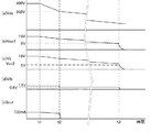
次にLED電源装置1の動作を説明する。まず、図2に比較例によるLED電源装置の入力電源オフ時(すなわち、消灯動作時)の各部波形を示す。比較例によるLED電源装置は、上記LED電源装置1から入力電源検出部60を除いたものである。図2は、(a)コンデンサ114の平滑電圧Vdc、(b)一次側制御電圧Vcc1、(c)二次側補助電圧Vs(実線)及び二次側制御電圧Vcc2(破線)、(d)駆動制御IC30のFB端子電圧Vfb、並びに(e)出力電流Iout(すなわちLED電流)を示し、横軸は時間である。なお、図は模式図であり、寸法通りではない。   Next, the operation of the LED power supply device 1 will be described. First, FIG. 2 shows waveforms of respective parts when the input power supply of the LED power supply device according to the comparative example is turned off (that is, during the extinguishing operation). The LED power supply device according to the comparative example is obtained by removing the input power supply detection unit 60 from the LED power supply device 1. FIG. 2 shows (a) the smoothing voltage Vdc of the capacitor 114, (b) the primary side control voltage Vcc1, (c) the secondary side auxiliary voltage Vs (solid line), and the secondary side control voltage Vcc2 (dashed line), (d) driving. The FB terminal voltage Vfb of the control IC 30 and (e) the output current Iout (that is, the LED current) are shown, and the horizontal axis is time. In addition, a figure is a schematic diagram and is not as the dimension.

時刻t1までは、平滑電圧Vdcは400V、一次側制御電圧Vcc1は18V、二次側補助電圧Vsは18V、二次側制御電圧Vcc2は5V、FB端子電圧Vfbは1.1V、出力電流Ioutは100mAであるものとする。全光時の出力電流は600mAであり、本例では、約17%の調光状態で入力電源がオフされる場合が例示される。なお、比較例及び各実施形態では、一次側の補助電源回路510の電圧供給能力は補助電源回路520のものとほぼ同等であるものとする。   Until time t1, the smoothing voltage Vdc is 400V, the primary side control voltage Vcc1 is 18V, the secondary side auxiliary voltage Vs is 18V, the secondary side control voltage Vcc2 is 5V, the FB terminal voltage Vfb is 1.1V, and the output current Iout is It shall be 100 mA. The output current during all light is 600 mA, and in this example, the case where the input power source is turned off in a dimming state of about 17% is exemplified. In the comparative example and each embodiment, the voltage supply capability of the auxiliary power circuit 510 on the primary side is substantially the same as that of the auxiliary power circuit 520.

時刻t1において、入力電源ACがオフされる。これにより、平滑電圧Vdcが低下し始め、二次側補助電圧Vsも低下し始める。一方、三端子レギュレータ523の入力電圧は動作可能電圧よりも高いので正常な動作を継続し、二次側制御電圧Vcc2は通常点灯時と同様に5Vに維持される。また、一次側制御電圧Vcc1も駆動制御IC30の動作可能電圧(例えば8V程度)よりも高いので通常点灯時と同様に動作を継続し、FB端子電圧Vfbは時刻t1以前と同様に1.1Vに維持される。ただし、平滑電圧Vdcの低下に伴い出力電流Ioutは減少していく。   At time t1, the input power supply AC is turned off. Thereby, the smoothing voltage Vdc begins to decrease, and the secondary side auxiliary voltage Vs also begins to decrease. On the other hand, since the input voltage of the three-terminal regulator 523 is higher than the operable voltage, the normal operation is continued, and the secondary control voltage Vcc2 is maintained at 5 V as in the normal lighting. Since the primary side control voltage Vcc1 is also higher than the operable voltage of the drive control IC 30 (for example, about 8V), the operation is continued in the same way as during normal lighting, and the FB terminal voltage Vfb is 1.1V as before time t1. Maintained. However, the output current Iout decreases as the smoothing voltage Vdc decreases.

時刻t2において、一次側制御電圧Vcc1が駆動制御IC30の動作可能電圧(8V程度)以上である一方で、二次側補助電圧Vsが三端子レギュレータ523の動作可能電圧を下回ることにより、二次側制御電圧Vcc2が低下を開始し、5V以下となる。これにより、フォトカプラ417のフォトダイオード及びフォトトランジスタの電流が減少し、FB端子電圧Vfbが上昇を開始する。   At time t2, the primary side control voltage Vcc1 is equal to or higher than the operable voltage (about 8V) of the drive control IC 30, while the secondary side auxiliary voltage Vs falls below the operable voltage of the three-terminal regulator 523. The control voltage Vcc2 starts to decrease and becomes 5V or less. As a result, the current of the photodiode and the phototransistor of the photocoupler 417 decreases, and the FB terminal voltage Vfb starts to increase.

時刻t2〜t3において、時刻t2以降のFB端子電圧Vfbの上昇に応じて、駆動制御IC30がPWM制御におけるオン幅を増加させ、出力電流Ioutが急峻に上昇する。この出力電流Ioutの急峻な上昇が閃光となる。時刻t2〜t3の閃光点灯により、コンデンサ114の電荷が一気に放電され、平滑電圧Vdcは瞬時に低下する。これにより、時刻t3において、LED2は消灯し、LED電源装置1は完全に停止する。なお、本例においては、時刻t1〜t2は数秒であり、時刻t2〜t3は数十m秒程度である。   At times t2 to t3, the drive control IC 30 increases the ON width in the PWM control according to the increase in the FB terminal voltage Vfb after time t2, and the output current Iout increases sharply. This steep rise in the output current Iout becomes a flash. By the flashing of light at times t2 to t3, the electric charge of the capacitor 114 is discharged all at once, and the smoothing voltage Vdc decreases instantaneously. Thereby, at time t3, the LED 2 is turned off, and the LED power supply device 1 is completely stopped. In this example, the times t1 to t2 are several seconds, and the times t2 to t3 are about several tens of milliseconds.

図3に、本実施形態によるLED電源装置1の入力電源オフ時(すなわち、消灯制御時)の各部波形を示す。図2と同様に、図3は、(a)コンデンサ114の平滑電圧Vdc、(b)一次側制御電圧Vcc1、(c)二次側補助電圧Vs(実線)及び二次側制御電圧Vcc2(破線)、(d)駆動制御IC30のFB端子電圧Vfb、並びに(e)出力電流Iout(すなわちLED電流)を示し、横軸は時間である。なお、図は模式図であり、寸法通りではない。   FIG. 3 shows the waveforms of the respective parts when the input power supply of the LED power supply device 1 according to the present embodiment is off (that is, during the extinction control). Similar to FIG. 2, FIG. 3 shows (a) the smoothing voltage Vdc of the capacitor 114, (b) the primary side control voltage Vcc1, (c) the secondary side auxiliary voltage Vs (solid line), and the secondary side control voltage Vcc2 (broken line). ), (D) The FB terminal voltage Vfb of the drive control IC 30 and (e) the output current Iout (that is, the LED current) are shown, and the horizontal axis is time. In addition, a figure is a schematic diagram and is not as the dimension.

図2の例と同様に、時刻t1までは、平滑電圧Vdcは400V、一次側制御電圧Vcc1は18V、二次側補助電圧Vsは18V、二次側制御電圧Vcc2は5V、FB端子電圧Vfbは1.1V、出力電流Ioutは100mAである。全光時の出力電流は600mAであり、約17%の調光状態で入力電源がオフされた状態が例示される。なお、出力電圧Voutは35V〜90V程度となる。   As in the example of FIG. 2, until time t1, the smoothing voltage Vdc is 400V, the primary side control voltage Vcc1 is 18V, the secondary side auxiliary voltage Vs is 18V, the secondary side control voltage Vcc2 is 5V, and the FB terminal voltage Vfb is The output current Iout is 1.1 mA and 100 mA. The output current at the time of all light is 600 mA, and the state where the input power source is turned off in the dimming state of about 17% is exemplified. The output voltage Vout is about 35V to 90V.

時刻t1において、入力電源ACがオフされる。これにより、入力電源検出部60からMCU423への入力が二次側制御電圧Vcc2の電圧で一定となり(図1参照)、MCU423はDAC424を介してオペアンプ412における電流基準値を低下させる。これにより、駆動制御IC30のFB端子電圧Vfbが1.1Vから0.8Vに低減される。なお、この状態において、実質的に電流フィードバックは作用していなくてもよく、例えば、最小の二次出力が維持される。このFB端子電圧Vfbの低下により、DC/DCコンバータ20の二次側(二次主巻線N2側)出力電圧はLED2の順方向降下電圧Vf未満となり、LED2は消灯する。その後もスイッチング素子201は、PWM制御のパルス幅を狭くした状態(例えば、最小パルス幅)で駆動を継続する。このスイッチング動作により、平滑電圧Vdc、一次側制御電圧Vcc1及び二次側補助電圧Vsが徐々に低下していく。この状態においては、スイッチング素子201の駆動におけるパルス幅は最小化されるものの平滑電圧Vdcが比較的高い状態となるため、一次側及び二次側制御電圧Vcc1及びVcc2の低下における傾斜は緩やかなものとなる。この時点では、三端子レギュレータ523の入力電圧は動作可能電圧よりも高いので正常な動作を継続し、二次側制御電圧Vccは通常点灯時と同様に5Vに維持される。また、一次側制御電圧Vcc1も駆動制御IC30の動作可能電圧(例えば8V程度)よりも高いので通常点灯時と同様に動作を継続する。   At time t1, the input power supply AC is turned off. As a result, the input from the input power supply detection unit 60 to the MCU 423 becomes constant at the secondary side control voltage Vcc2 (see FIG. 1), and the MCU 423 decreases the current reference value in the operational amplifier 412 via the DAC 424. Thereby, the FB terminal voltage Vfb of the drive control IC 30 is reduced from 1.1V to 0.8V. In this state, the current feedback does not have to act substantially. For example, the minimum secondary output is maintained. Due to the decrease in the FB terminal voltage Vfb, the output voltage on the secondary side (secondary main winding N2 side) of the DC / DC converter 20 becomes less than the forward voltage drop Vf of the LED 2, and the LED 2 is turned off. Thereafter, the switching element 201 continues to be driven in a state where the pulse width of the PWM control is narrowed (for example, the minimum pulse width). By this switching operation, the smoothing voltage Vdc, the primary side control voltage Vcc1, and the secondary side auxiliary voltage Vs gradually decrease. In this state, the pulse width in driving the switching element 201 is minimized, but the smoothing voltage Vdc is relatively high, so that the slopes of the primary and secondary control voltages Vcc1 and Vcc2 are gradually lowered. It becomes. At this time, since the input voltage of the three-terminal regulator 523 is higher than the operable voltage, the normal operation is continued, and the secondary control voltage Vcc is maintained at 5 V as in the normal lighting. Further, since the primary side control voltage Vcc1 is also higher than the operable voltage of the drive control IC 30 (for example, about 8V), the operation is continued in the same manner as during normal lighting.

時刻t2において、一次側制御電圧Vcc1が駆動制御IC30の動作可能電圧(8V)を下回ると(本例においては、時刻t2において、二次側制御電圧Vcc2は5Vであるものとする)、駆動制御IC30及びスイッチング素子201の駆動が停止され、LED電源装置1の全体の動作が停止する。時刻t1から時刻t2までの時間は、本例では30秒〜50秒程度となる。   When the primary control voltage Vcc1 falls below the operable voltage (8 V) of the drive control IC 30 at time t2 (in this example, the secondary control voltage Vcc2 is 5 V at time t2), drive control is performed. The driving of the IC 30 and the switching element 201 is stopped, and the entire operation of the LED power supply device 1 is stopped. The time from time t1 to time t2 is about 30 to 50 seconds in this example.

なお、図3に示す例では、時刻t2の時点で、一次側制御電圧Vcc1が給電される駆動制御部30が、二次側制御電圧Vcc2が給電される出力制御部40よりも先に動作を停止する例を示したが、動作停止の順序が逆であってもよい。図4に、二次側制御電圧Vcc2が給電される出力制御部40が、一次側制御電圧Vcc1が給電される駆動制御部30よりも先に動作を停止する例を示す。   In the example shown in FIG. 3, at time t2, the drive control unit 30 to which the primary control voltage Vcc1 is fed operates before the output control unit 40 to which the secondary control voltage Vcc2 is fed. Although an example of stopping is shown, the order of operation stop may be reversed. FIG. 4 shows an example in which the output control unit 40 to which the secondary control voltage Vcc2 is fed stops operating before the drive control unit 30 to which the primary control voltage Vcc1 is fed.

図3と同様に、図4は(a)コンデンサ114の平滑電圧Vdc、(b)一次側制御電圧Vcc1、(c)二次側補助電圧Vs(実線)及び二次側制御電圧Vcc2(破線)、(d)駆動制御IC30のFB端子電圧Vfb、並びに(e)出力電流Iout(すなわちLED電流)を示し、横軸は時間である。なお、図は模式図であり、寸法通りではない。   Similar to FIG. 3, FIG. 4 shows (a) the smoothing voltage Vdc of the capacitor 114, (b) the primary side control voltage Vcc1, (c) the secondary side auxiliary voltage Vs (solid line), and the secondary side control voltage Vcc2 (dashed line). , (D) shows the FB terminal voltage Vfb of the drive control IC 30 and (e) the output current Iout (that is, the LED current), and the horizontal axis represents time. In addition, a figure is a schematic diagram and is not as the dimension.

図3の例と同様に、時刻t1までは、平滑電圧Vdcは400V、一次側制御電圧Vcc1は18V、二次側補助電圧Vsは18V、二次側制御電圧Vcc2は5V、FB端子電圧Vfbは1.1V、出力電流Ioutは100mAである。全光時の出力電流は600mAであり、約17%の調光状態で入力電源がオフされた状態が例示される。   Similar to the example of FIG. 3, until time t1, the smoothing voltage Vdc is 400V, the primary side control voltage Vcc1 is 18V, the secondary side auxiliary voltage Vs is 18V, the secondary side control voltage Vcc2 is 5V, and the FB terminal voltage Vfb is The output current Iout is 1.1 mA and 100 mA. The output current at the time of all light is 600 mA, and the state where the input power source is turned off in the dimming state of about 17% is exemplified.

時刻t1において、図3の例と同様に、入力電源ACがオフされると、駆動制御IC30のFB端子電圧Vfbが1.1Vから0.8Vに低減され、DC/DCコンバータ20の二次側(二次主巻線N2側)出力電圧はLED2の順方向降下電圧Vf未満となり、LED2が消灯する。その後もスイッチング素子201は、PWM制御のパルス幅を狭くした状態(例えば、最小パルス幅)で駆動を継続する。このスイッチング動作により、平滑電圧Vdc、一次側制御電圧Vcc1及び二次側補助電圧Vsが徐々に低下していく。なお、三端子レギュレータ523の入力電圧は動作可能電圧よりも高いので正常な動作を継続し、二次側制御電圧Vccは通常点灯時と同様に5Vに維持される。また、一次側制御電圧Vcc1も駆動制御IC30の動作可能電圧(例えば8V程度)よりも高いので通常点灯時と同様に動作を継続する。   At time t1, as in the example of FIG. 3, when the input power supply AC is turned off, the FB terminal voltage Vfb of the drive control IC 30 is reduced from 1.1V to 0.8V, and the secondary side of the DC / DC converter 20 (Secondary main winding N2 side) The output voltage becomes less than the forward voltage drop Vf of the LED 2, and the LED 2 is turned off. Thereafter, the switching element 201 continues to be driven in a state where the pulse width of the PWM control is narrowed (for example, the minimum pulse width). By this switching operation, the smoothing voltage Vdc, the primary side control voltage Vcc1, and the secondary side auxiliary voltage Vs gradually decrease. Since the input voltage of the three-terminal regulator 523 is higher than the operable voltage, the normal operation is continued, and the secondary control voltage Vcc is maintained at 5 V as in the normal lighting. Further, since the primary side control voltage Vcc1 is also higher than the operable voltage of the drive control IC 30 (for example, about 8V), the operation is continued in the same manner as during normal lighting.

時刻t2において、一次側制御電圧Vcc1は動作可能電圧(8V)以上である状態で、二次側制御電圧Vcc2が低下すると、比較例の場合と同様に、FB端子電圧Vfbは急峻に上昇する。しかし、時刻t1〜t2までの動作により、平滑電圧Vdcが充分に低下しているので、LED2の再点灯乃至は閃光点灯は起こらない。言い換えると、LED2の順方向降下電圧をVf、一次主巻線N1の巻数をT1、二次主巻線N2の巻数をT2とした場合に、時刻t2までに、Vdc<Vf×(T2/T1)、となっていれば、LED2に閃光は発生し得ない。   At time t2, when the secondary side control voltage Vcc2 decreases in a state where the primary side control voltage Vcc1 is equal to or higher than the operable voltage (8V), the FB terminal voltage Vfb rises steeply as in the comparative example. However, since the smoothing voltage Vdc is sufficiently lowered by the operation from time t1 to time t2, the LED 2 is not re-lit or flashed. In other words, when the forward voltage drop of LED2 is Vf, the number of turns of the primary main winding N1 is T1, and the number of turns of the secondary main winding N2 is T2, Vdc <Vf × (T2 / T1) by time t2. ), No flash can occur in the LED 2.

図3及び図4に関して上述したように、入力電源停止後に、トランス202を介したコンデンサ114のエネルギーの供給比率に関して、二次主巻線N2に接続されたLED2側に対する供給(第1の二次出力)に対する、二次補助巻線N3及びN4が接続された制御部(30、40、50)側に対する供給(第2の二次出力)が増加する。これにより、比較例に示したような、二次側出力制御が効かない状態でコンデンサ114のエネルギーが消灯間際のLED2において一気に放出される閃光現象が防止される。   As described above with reference to FIGS. 3 and 4, after the input power supply is stopped, the supply ratio of the energy of the capacitor 114 via the transformer 202 is supplied to the LED2 side connected to the secondary main winding N2 (first secondary The output (second secondary output) to the control unit (30, 40, 50) to which the secondary auxiliary windings N3 and N4 are connected increases. As a result, the flashing phenomenon in which the energy of the capacitor 114 is released at once in the LED 2 just before extinguishing in the state where the secondary output control is not effective as shown in the comparative example is prevented.

なお、上記においては、調光率が17%の場合について説明したが、本発明は他の調光率における消灯制御についても同様に実施できる。ただし、調光率が浅い(明るい)場合又は全光時には、入力電源ACの遮断直後のスイッチング素子201の駆動によりコンデンサ114の電圧が直ちに放電されるのでコンデンサ114の残電圧をエネルギー源とする閃光は起こりにくい。したがって、調光率が所定の調光率以下である場合に、上述したような入力電源オフ時のLED2への出力低減制御が行われるようにしてもよい。例えば、この所定の調光率は、20%程度であればよい。   In the above description, the case where the dimming rate is 17% has been described. However, the present invention can be similarly applied to the turn-off control at other dimming rates. However, when the dimming rate is shallow (bright) or all lights, the voltage of the capacitor 114 is immediately discharged by driving the switching element 201 immediately after the input power supply AC is cut off, so that the flash using the residual voltage of the capacitor 114 as an energy source. Is unlikely to occur. Therefore, when the dimming rate is equal to or lower than the predetermined dimming rate, the above-described output reduction control to the LED 2 when the input power is off may be performed. For example, the predetermined dimming rate may be about 20%.

以上のように、本実施形態によるLED電源装置1によると以下の効果が得られる。
(1)閃光の防止
本実施形態では、入力電源検出部60によって交流入力電圧ACの停止が検出された場合に、制御部(30、40、50)は、DC/DCコンバータ20から制御部への二次出力(第2の二次出力)に対するDC/DCコンバータ20からLED2への二次出力(第1の二次出力)の割合を低減するようにスイッチング素子201の駆動を制御する。したがって、入力電源遮断後に、DC/DCコンバータ20の一次側のコンデンサ114の残存エネルギーがLED2において一気に放出される状態が回避され、LED消灯直前の閃光が防止される。特に、交流入力電圧ACの停止が検出された場合にLED2への出力電圧がその順方向降下電圧Vf未満となるようにスイッチング素子201が駆動制御されるので、確実にLED2における閃光が防止される。
As described above, according to the LED power supply device 1 according to the present embodiment, the following effects can be obtained.
(1) Flash prevention In this embodiment, when the stop of the AC input voltage AC is detected by the input power supply detection unit 60, the control unit (30, 40, 50) is transferred from the DC / DC converter 20 to the control unit. The driving of the switching element 201 is controlled so as to reduce the ratio of the secondary output (first secondary output) from the DC / DC converter 20 to the LED 2 with respect to the secondary output (second secondary output). Therefore, a state in which the residual energy of the capacitor 114 on the primary side of the DC / DC converter 20 is released at a stroke after the input power is shut off is avoided, and flashing immediately before the LED is turned off is prevented. In particular, since the switching element 201 is driven and controlled so that the output voltage to the LED 2 becomes less than the forward drop voltage Vf when the stop of the AC input voltage AC is detected, flashing in the LED 2 is surely prevented. .

(2)高い応答性
また、本実施形態では、入力電源検出部60及びMCU423が、入力電源電圧に基づく脈流出力に基づいてその停止を検出するように構成される。これにより、入力電源停止から数十ms程度で速やかに上記の消灯制御が開始され、高い応答性で閃光が防止される。
(2) High Responsiveness In the present embodiment, the input power supply detection unit 60 and the MCU 423 are configured to detect the stop based on the pulsating flow output based on the input power supply voltage. As a result, the above-described extinguishing control is started promptly within several tens of ms after the input power supply is stopped, and flashing is prevented with high responsiveness.

(3)適時な消灯制御
さらに、本実施形態では、調光率が所定の調光率以下の場合でかつ入力電圧ACの停止が検出された場合に上記の消灯制御が行われる。したがって、閃光のおそれがない点灯状態(例えば全光時)においては、入力電源停止後に比較的早くLED電源装置1を停止させることができる。
(3) Timely extinction control Further, in the present embodiment, the above extinction control is performed when the dimming rate is equal to or lower than the predetermined dimming rate and when the stop of the input voltage AC is detected. Therefore, in the lighting state where there is no fear of flashing (for example, in the case of all light), the LED power supply device 1 can be stopped relatively quickly after the input power supply is stopped.

実施形態2.
第1の実施形態では、AC/DC変換部10が力率改善回路を含む構成を示したが、本実施形態では、AC/DC変換部10がいわゆるコンデンサインプット型の回路からなる構成を示す。図5に、本実施形態によるLED電源装置1及びそれを用いたLED照明装置3の回路図を示す。図1に示す第1の実施形態との相違は、AC/DC変換部10及び入力電源検出部60にある。なお、図5において、図1と同様の符号が付された要素は、特に断りがない限り図1と実質的に同様の要素を示すものとし、その詳細な説明を省略する。
Embodiment 2. FIG.
In the first embodiment, the configuration in which the AC / DC conversion unit 10 includes the power factor correction circuit is shown. However, in the present embodiment, the AC / DC conversion unit 10 is configured by a so-called capacitor input type circuit. In FIG. 5, the circuit diagram of the LED power supply device 1 by this embodiment and the LED lighting apparatus 3 using the same is shown. The difference from the first embodiment shown in FIG. 1 resides in the AC / DC converter 10 and the input power source detector 60. 5, elements denoted by the same reference numerals as those in FIG. 1 are substantially the same as those in FIG. 1 unless otherwise specified, and detailed description thereof is omitted.

AC/DC変換部10は、全波整流器101及びコンデンサ114を含み、全波整流器101の出力端が直接コンデンサ114に接続される。入力電源検出部60は、フォトカプラ601、抵抗602、抵抗603及び全波整流器604(整流器)を備える。AC/DC変換部10において、全波整流器101の出力はコンデンサ114によって平滑されるため、全波整流器101の出力端においては、入力電源ACの電圧を脈流状態で(すなわち、遅延なく)検出することができない。そこで、全波整流器604が入力電源ACと全波整流器101の間のACラインに接続され、入力電源電圧を全波整流した脈流出力がフォトカプラ601に入力される。全波整流器604に流れる電流は抵抗602によって制限されるので、全波整流器604には全波整流器101よりも電流容量の小さい素子を用いることができる。   The AC / DC converter 10 includes a full-wave rectifier 101 and a capacitor 114, and an output terminal of the full-wave rectifier 101 is directly connected to the capacitor 114. The input power supply detection unit 60 includes a photocoupler 601, a resistor 602, a resistor 603, and a full-wave rectifier 604 (rectifier). In the AC / DC converter 10, the output of the full-wave rectifier 101 is smoothed by the capacitor 114, so that the voltage of the input power supply AC is detected in a pulsating state (that is, without delay) at the output terminal of the full-wave rectifier 101. Can not do it. Therefore, the full-wave rectifier 604 is connected to the AC line between the input power supply AC and the full-wave rectifier 101, and a pulsating output obtained by full-wave rectifying the input power supply voltage is input to the photocoupler 601. Since the current flowing through the full-wave rectifier 604 is limited by the resistor 602, an element having a smaller current capacity than the full-wave rectifier 101 can be used for the full-wave rectifier 604.

なお、図6Aに一変形例として示すように、全波整流器604の代わりにダイオード605(整流器)が接続される構成としてもよい。この場合、ダイオード605のアノードが一方のACラインに接続され、フォトカプラ601のフォトダイオードのカソードが他方のACラインに接続され、フォトカプラ601には半波整流波形が入力される。フォトカプラ601からMCU423への入力は入力電源電圧の半波整流波形に基づくため、入力電源電圧のオン/オフは、入力電源電圧の1サイクル以内(50Hzの場合には、20ms以内)に検出され得る。なお、検出精度を高めるために入力電源電圧の数サイクル〜数十サイクルに対応する期間(例えば、数十ms〜数百ms)が判定期間として設定されてもよい。   6A, a diode 605 (rectifier) may be connected instead of the full-wave rectifier 604. As shown in FIG. In this case, the anode of the diode 605 is connected to one AC line, the cathode of the photodiode of the photocoupler 601 is connected to the other AC line, and a half-wave rectified waveform is input to the photocoupler 601. Since the input from the photocoupler 601 to the MCU 423 is based on a half-wave rectified waveform of the input power supply voltage, the on / off of the input power supply voltage is detected within one cycle of the input power supply voltage (within 20 ms for 50 Hz). obtain. In order to improve detection accuracy, a period corresponding to several cycles to several tens of cycles of the input power supply voltage (for example, several tens of milliseconds to several hundreds of milliseconds) may be set as the determination period.

あるいは、図6Bに他の変形例として示すように、全波整流器604及びダイオード605を接続せずに、フォトカプラ601の代わりにACフォトカプラ606が接続される構成としてもよい。この場合、ACフォトカプラ606の並列フォトダイオードが抵抗602を介してACラインに接続される。   Alternatively, as shown in FIG. 6B as another modification, the AC photocoupler 606 may be connected instead of the photocoupler 601 without connecting the full-wave rectifier 604 and the diode 605. In this case, the parallel photodiode of the AC photocoupler 606 is connected to the AC line via the resistor 602.

図5、図6A及び図6Bに示す形態において、入力電源オフ時の消灯制御は、図3又は図4に示した第1の実施形態のものと同様である。これにより、本実施形態においても、第1の実施形態に関して上述した効果(1)閃光の防止、(2)高い応答性、及び(3)適時な消灯制御と同様の効果を得ることができる。   In the form shown in FIGS. 5, 6A, and 6B, the turn-off control when the input power is off is the same as that of the first embodiment shown in FIG. 3 or FIG. Thereby, also in this embodiment, the same effects as the effects (1) prevention of flash, (2) high responsiveness, and (3) timely turn-off control described above with respect to the first embodiment can be obtained.

実施形態3.
上記第1及び第2の実施形態では、入力電源検出部60が入力電源ACによる脈流出力を検出する構成を示したが、本実施形態では、入力電源検出部60がコンデンサ114の平滑電圧を検出する構成を示す。図7に、本実施形態によるLED電源装置1及びそれを用いたLED照明装置3の回路図を示す。図1に示す第1の実施形態との相違は、入力電源検出部60の接続及びMCU423の動作にある。なお、図7において、図1と同様の符号が付された要素は、特に断りがない限り図1と実質的に同様の要素を示すものとし、その詳細な説明を省略する。
Embodiment 3. FIG.
In the first and second embodiments, the configuration in which the input power source detection unit 60 detects the pulsating output from the input power source AC is shown. However, in this embodiment, the input power source detection unit 60 uses the smoothed voltage of the capacitor 114. The structure to detect is shown. In FIG. 7, the circuit diagram of the LED power supply device 1 by this embodiment and the LED lighting apparatus 3 using the same is shown. The difference from the first embodiment shown in FIG. 1 is in the connection of the input power source detection unit 60 and the operation of the MCU 423. 7, elements denoted by the same reference numerals as those in FIG. 1 are substantially the same as those in FIG. 1 unless otherwise specified, and detailed description thereof is omitted.

入力電源検出部60の抵抗602はコンデンサ114の正極端に接続される。これにより、フォトカプラ601のフォトダイオード及びフォトトランジスタには直流電流が流れ、MCU423には直流電圧が入力される。MCU423は、フォトカプラ601からの入力電圧が所定値を超えると(すなわち、コンデンサ114の平滑電圧Vdcが閾値を下回ると)上記の消灯制御を行うように構成される。したがって、MCU423における演算は簡素なものでよい。なお、閾値は通常点灯時の平滑電圧Vdcの80〜90%程度の電圧であればよい。   The resistor 602 of the input power source detection unit 60 is connected to the positive terminal of the capacitor 114. As a result, a direct current flows through the photodiode and the phototransistor of the photocoupler 601, and a direct current voltage is input to the MCU 423. The MCU 423 is configured to perform the above-described extinguishing control when the input voltage from the photocoupler 601 exceeds a predetermined value (that is, when the smoothed voltage Vdc of the capacitor 114 falls below a threshold value). Therefore, the calculation in the MCU 423 may be simple. The threshold value may be a voltage that is about 80 to 90% of the smoothing voltage Vdc during normal lighting.

図8に、本実施形態によるLED電源装置1の入力電源オフ時(すなわち、消灯制御時)の各部波形を示す。図3と同様に、図8は、(a)コンデンサ114の平滑電圧Vdc、(b)一次側制御電圧Vcc1、(c)二次側補助電圧Vs(実線)及び二次側制御電圧Vcc2(破線)、(d)駆動制御IC30のFB端子電圧Vfb、並びに(e)出力電流Iout(すなわちLED電流)を示し、横軸は時間である。なお、図は模式図であり、寸法通りではない。   FIG. 8 shows respective waveforms of the LED power supply device 1 according to the present embodiment when the input power is turned off (that is, during extinguishing control). Similar to FIG. 3, FIG. 8 shows (a) the smoothing voltage Vdc of the capacitor 114, (b) the primary side control voltage Vcc1, (c) the secondary side auxiliary voltage Vs (solid line), and the secondary side control voltage Vcc2 (broken line). ), (D) The FB terminal voltage Vfb of the drive control IC 30 and (e) the output current Iout (that is, the LED current) are shown, and the horizontal axis is time. In addition, a figure is a schematic diagram and is not as the dimension.

図3の例と同様に、時刻t1までは、平滑電圧Vdcは400V、一次側制御電圧Vcc1は18V、二次側補助電圧Vsは18V、二次側制御電圧Vcc2は5V、FB端子電圧Vfbは1.1V、出力電流Ioutは100mAである。全光時の出力電流は600mAであり、約17%の調光状態で入力電源がオフされた状態が例示される。なお、出力電圧Voutは35V〜90V程度となる。   Similar to the example of FIG. 3, until time t1, the smoothing voltage Vdc is 400V, the primary side control voltage Vcc1 is 18V, the secondary side auxiliary voltage Vs is 18V, the secondary side control voltage Vcc2 is 5V, and the FB terminal voltage Vfb is The output current Iout is 1.1 mA and 100 mA. The output current at the time of all light is 600 mA, and the state where the input power source is turned off in the dimming state of about 17% is exemplified. The output voltage Vout is about 35V to 90V.

時刻t1において、入力電源ACがオフされる。これにより、図2に示す比較例の場合と同様に、平滑電圧Vdcが低下し始め、二次側補助電圧Vsも低下し始める。一方、三端子レギュレータ523の入力電圧は動作可能電圧よりも高いので正常な動作を継続し、二次側制御電圧Vcc2は通常点灯時と同様に5Vに維持される。また、一次側制御電圧Vcc1も駆動制御IC30の動作可能電圧(例えば8V程度)よりも高いので通常点灯時と同様に動作を継続し、FB端子電圧Vfbは時刻t1以前と同様に1.1Vに維持される。ただし、平滑電圧Vdcの低下に伴い出力電流Ioutは減少していく。   At time t1, the input power supply AC is turned off. As a result, as in the case of the comparative example shown in FIG. 2, the smoothing voltage Vdc begins to decrease, and the secondary side auxiliary voltage Vs also begins to decrease. On the other hand, since the input voltage of the three-terminal regulator 523 is higher than the operable voltage, the normal operation is continued, and the secondary control voltage Vcc2 is maintained at 5 V as in the normal lighting. Since the primary side control voltage Vcc1 is also higher than the operable voltage of the drive control IC 30 (for example, about 8V), the operation is continued in the same way as during normal lighting, and the FB terminal voltage Vfb is 1.1V as before time t1. Maintained. However, the output current Iout decreases as the smoothing voltage Vdc decreases.

時刻t2において、平滑電圧Vdcが閾値(例えば、350V)を下回ると、この状態が入力電源検出部60及びMCU423によって検出され、MCU423はDAC424を介してオペアンプ412における電流基準値を低下させる。これにより、駆動制御IC30のFB端子電圧Vfbが1.1Vから0.8Vに低減される。このFB端子電圧Vfbの低下により、DC/DCコンバータ20の二次側(二次主巻線N2側)出力電圧はLED2の順方向降下電圧Vf未満となり、LED2は消灯する。その後もスイッチング素子201は、PWM制御のパルス幅を狭くした状態(例えば、最小パルス幅)で駆動を継続する。このスイッチング動作により、平滑電圧Vdc、一次側制御電圧Vcc1及び二次側補助電圧Vsが徐々に低下していく。なお、三端子レギュレータ523の入力電圧は動作可能電圧よりも高いので正常な動作を継続し、二次側制御電圧Vccは通常点灯時と同様に5Vに維持される。また、一次側制御電圧Vcc1も駆動制御IC30の動作可能電圧(例えば8V程度)よりも高いので通常点灯時と同様に動作を継続する。   When the smoothed voltage Vdc falls below a threshold value (for example, 350 V) at time t <b> 2, this state is detected by the input power supply detection unit 60 and the MCU 423, and the MCU 423 decreases the current reference value in the operational amplifier 412 via the DAC 424. Thereby, the FB terminal voltage Vfb of the drive control IC 30 is reduced from 1.1V to 0.8V. Due to the decrease in the FB terminal voltage Vfb, the output voltage on the secondary side (secondary main winding N2 side) of the DC / DC converter 20 becomes less than the forward voltage drop Vf of the LED 2, and the LED 2 is turned off. Thereafter, the switching element 201 continues to be driven in a state where the pulse width of the PWM control is narrowed (for example, the minimum pulse width). By this switching operation, the smoothing voltage Vdc, the primary side control voltage Vcc1, and the secondary side auxiliary voltage Vs gradually decrease. Since the input voltage of the three-terminal regulator 523 is higher than the operable voltage, the normal operation is continued, and the secondary control voltage Vcc is maintained at 5 V as in the normal lighting. Further, since the primary side control voltage Vcc1 is also higher than the operable voltage of the drive control IC 30 (for example, about 8V), the operation is continued in the same manner as during normal lighting.

時刻t3において、一次側制御電圧Vcc1が駆動制御IC30の動作可能電圧(8V)を下回ると(本例においては、時刻t3において二次側制御電圧Vcc2は5V以上であるものとする)、駆動制御IC30及びスイッチング素子201の駆動が停止され、LED電源装置1の全体の動作が停止する。時刻t1〜t3の時間は、時刻t1〜t2においてコンデンサ114のエネルギーがLED2で放出された分だけ、第1の実施形態(図3)の時刻t1〜t2までの時間よりも若干短くなる。   When the primary control voltage Vcc1 falls below the operable voltage (8 V) of the drive control IC 30 at time t3 (in this example, the secondary control voltage Vcc2 is 5 V or more at time t3), drive control The driving of the IC 30 and the switching element 201 is stopped, and the entire operation of the LED power supply device 1 is stopped. The time from the time t1 to the time t3 is slightly shorter than the time from the time t1 to the time t2 in the first embodiment (FIG. 3) by the amount that the energy of the capacitor 114 is released by the LED 2 at the time t1 to t2.

なお、第1の実施形態の図4に示す例と同様に、出力制御部40の動作停止が駆動制御部30の動作停止よりも先に起こる場合であっても閃光は起こらない。逆に、平滑電圧Vdc<順方向降下電圧Vf×(二次主巻線N2ターン数T2/一次主巻線N1ターン数T1)となった時点で出力制御部40が駆動制御部30に最大デューティ(最大オン幅)でスイッチング素子201を駆動させるようにしてもよい。これにより、閃光の可能性がなくなった時点でコンデンサ114の残電圧を放電させ、迅速に消灯制御を終了させることができる。   As in the example shown in FIG. 4 of the first embodiment, even if the operation stop of the output control unit 40 occurs before the operation stop of the drive control unit 30, no flashing occurs. Conversely, when the smoothing voltage Vdc <forward voltage drop Vf × (secondary main winding N2 number of turns T2 / primary main winding N1 number of turns T1), the output control unit 40 applies the maximum duty to the drive control unit 30. The switching element 201 may be driven with (maximum ON width). As a result, the remaining voltage of the capacitor 114 can be discharged when the possibility of flashing disappears, and the extinguishing control can be terminated quickly.

以上より、本実施形態においても、第1の実施形態に関して上述した効果(1)閃光の防止及び(3)適時な消灯制御に加えて、以下の効果(4)を得ることができる。なお、本実施形態は第2の実施形態(コンデンサインプット型回路)に適用することもできる。   As described above, in this embodiment as well, the following effect (4) can be obtained in addition to the effect (1) flash prevention and (3) timely turn-off control described above with respect to the first embodiment. The present embodiment can also be applied to the second embodiment (capacitor input type circuit).

(4)設計自由度の向上
本実施形態によると、入力電源検出部60の出力は直流となる。従って、出力制御部40における電流基準値切換え構成に設計の自由度が増す。例えば、フォトカプラ601のフォトトランジスタのコレクタ電圧が所定値を超えると(すなわち、平滑電圧Vdcが閾値未満となると)抵抗414に追加の抵抗が並列接続されて電流基準値が低減される構成等とすることができる。
(4) Improvement in design freedom According to the present embodiment, the output of the input power source detection unit 60 is a direct current. Therefore, the degree of freedom of design increases in the current reference value switching configuration in the output control unit 40. For example, when the collector voltage of the phototransistor of the photocoupler 601 exceeds a predetermined value (that is, when the smoothing voltage Vdc is less than the threshold value), an additional resistor is connected in parallel to the resistor 414, and the current reference value is reduced. can do.

<変形例>
以上に本発明の好適な実施形態を示したが、本発明は、例えば以下に示すように種々の態様に変形可能である。
<Modification>
Although preferred embodiments of the present invention have been described above, the present invention can be modified into various modes as shown below, for example.

(1)DC/DCコンバータ20の変形
上記各実施形態においては、DC/DCコンバータ20として、フライバックコンバータを示したが、DC/DCコンバータ20は他の方式のコンバータからなるスイッチング電源回路であってもよい。例えば、DC/DCコンバータ20は、フォワード型コンバータ、非絶縁型の降圧チョッパ回路等であってもよい。
(1) Modification of DC / DC Converter 20 In each of the above-described embodiments, a flyback converter is shown as the DC / DC converter 20, but the DC / DC converter 20 is a switching power supply circuit composed of a converter of another type. May be. For example, the DC / DC converter 20 may be a forward converter, a non-insulated step-down chopper circuit, or the like.

(2)出力制御部40の変形
上記各実施形態においては、出力制御部40が定電流制御(電流フィードバック制御)を行う構成を示したが、駆動制御部30の出力を制限できれば定電流制御は行われなくてもよい。例えば、出力制御部40が出力電流をフィードフォワード制御する構成であっても本発明の有利な効果を享受できる。また、上記各実施形態では、消灯制御においては第1の二次出力の電圧をLED2の順方向降下電圧Vf未満としてLED2を消灯させる構成としたが、閃光が防止される範囲で第1の二次出力の電圧を順方向降下電圧Vf付近としてLED2を減光させる構成としてもよい。
(2) Modification of output control unit 40 In each of the above embodiments, the configuration in which the output control unit 40 performs constant current control (current feedback control) has been described. However, if the output of the drive control unit 30 can be limited, the constant current control is performed. It does not have to be done. For example, even if the output control unit 40 is configured to feedforward control the output current, the advantageous effects of the present invention can be enjoyed. In each of the above-described embodiments, in the extinguishing control, the LED 2 is extinguished by setting the voltage of the first secondary output to be less than the forward drop voltage Vf of the LED 2. However, the first second output is within the range in which flashing is prevented. The LED 2 may be dimmed by setting the next output voltage in the vicinity of the forward voltage drop Vf.

(3)補助電源部50の変形1
上記各実施形態においては、補助電源部50の一次側の補助電源回路510が二次補助巻線N3から制御電源を生成する構成を示したが、スイッチング素子201に対して設けられたスナバ回路から制御電源を生成する構成としてもよい。例えば、図9に示すように、スイッチング素子201のドレイン端子にコンデンサ513が接続され、ソース端子(一次グランド)にダイオード514のアノードが接続される。そして、コンデンサ513とダイオード514の接続点がダイオード515のアノードに接続され、ダイオード515のカソードがコンデンサ512の正極端に接続される。これにより、スイッチング素子201のオン/オフ時にコンデンサ513に発生するパルス状の電圧を一次側制御電圧Vcc1の生成に利用することができる。なお、コンデンサ513に発生する電圧、すなわち、補助電源回路510の電源生成能力は、(平滑電圧Vdcが同じであれば)スイッチング素子201の駆動におけるパルス幅ではなくスイッチング周波数に依存する。したがって、消灯制御時にスイッチング素子201の駆動パルス幅を狭めても一次側電源電圧Vcc1の供給能力が比較的高い状態で確保される。
(3) Modification 1 of the auxiliary power supply unit 50
In each of the embodiments described above, the auxiliary power supply circuit 510 on the primary side of the auxiliary power supply unit 50 generates the control power from the secondary auxiliary winding N3. However, from the snubber circuit provided for the switching element 201 It is good also as a structure which produces | generates control power supply. For example, as shown in FIG. 9, the capacitor 513 is connected to the drain terminal of the switching element 201, and the anode of the diode 514 is connected to the source terminal (primary ground). The connection point between the capacitor 513 and the diode 514 is connected to the anode of the diode 515, and the cathode of the diode 515 is connected to the positive terminal of the capacitor 512. Thereby, the pulsed voltage generated in the capacitor 513 when the switching element 201 is turned on / off can be used to generate the primary control voltage Vcc1. Note that the voltage generated in the capacitor 513, that is, the power generation capability of the auxiliary power circuit 510 depends on the switching frequency rather than the pulse width in driving the switching element 201 (if the smoothing voltage Vdc is the same). Therefore, even when the drive pulse width of the switching element 201 is narrowed during the extinction control, the supply capability of the primary power supply voltage Vcc1 is ensured in a relatively high state.

(4)補助電源部50の変形2
上記各実施形態においては、二次側補助電圧Vsから二次側制御電圧Vcc2を生成するレギュレータ回路として三端子レギュレータ523を用いたが、シリーズレギュレータによる降圧回路を用いてもよいし、降圧チョッパ回路、リンギングチョークコンバータ回路等を用いてもよい。また、上記各実施形態においては、DC/DCコンバータ20がフライバックコンバータで構成され、一次側制御電圧Vcc1及び二次側補助電圧Vsが、フライバックコンバータのトランスの補助巻線から生成される構成を示したが、これらの制御電圧が生成される構成はこれに限られない。例えば、DC/DCコンバータ20がフォワード型コンバータからなる場合には、一次側制御電圧Vcc1及び二次側補助電圧Vsは、トランス二次巻線に直列接続されるチョークコイルに設けられた補助巻線から生成されるようにすることもできる。
(4) Modification 2 of the auxiliary power supply unit 50
In each of the above embodiments, the three-terminal regulator 523 is used as a regulator circuit that generates the secondary side control voltage Vcc2 from the secondary side auxiliary voltage Vs. However, a step-down circuit using a series regulator may be used, or a step-down chopper circuit. A ringing choke converter circuit or the like may be used. In each of the above embodiments, the DC / DC converter 20 is constituted by a flyback converter, and the primary control voltage Vcc1 and the secondary auxiliary voltage Vs are generated from the auxiliary winding of the transformer of the flyback converter. However, the configuration in which these control voltages are generated is not limited to this. For example, when the DC / DC converter 20 is a forward type converter, the primary side control voltage Vcc1 and the secondary side auxiliary voltage Vs are auxiliary windings provided in a choke coil connected in series to the transformer secondary winding. It can also be generated from.

1 LED電源装置
2 LED
3 LED照明装置
10 AC/DC変換部
20 DC/DCコンバータ
30 駆動制御部
40 出力制御部
50 補助電源部
60 入力電源検出部
101 全波整流器
110 力率改善回路
114 コンデンサ(平滑コンデンサ)
201 スイッチング素子
202 トランス
604 全波整流器(整流器)
605 ダイオード(整流器)

1 LED power supply 2 LED
3 LED lighting device 10 AC / DC converter 20 DC / DC converter 30 Drive controller 40 Output controller 50 Auxiliary power source 60 Input power source detector 101 Full wave rectifier 110 Power factor improving circuit 114 Capacitor (smoothing capacitor)
201 switching element 202 transformer 604 full-wave rectifier (rectifier)
605 Diode (rectifier)

Claims (9)

LED電源装置であって、
交流入力電圧を直流変換して平滑コンデンサを充電するAC/DC変換部と、
一次側のスイッチング素子のスイッチング動作によって前記平滑コンデンサの電圧を変圧して、変圧された第1の二次出力をLEDに供給するDC/DCコンバータと、
前記交流入力電圧を検出する入力電源検出部と、
前記DC/DCコンバータの第2の二次出力が給電されて前記スイッチング素子を駆動するように構成され、前記交流入力電圧の停止が検出された場合に、前記スイッチング素子の駆動を継続させて前記第2の二次出力が供給される状態で前記第2の二次出力に対する前記第1の二次出力の割合を低減するように前記スイッチング素子の駆動を制御する制御部と
を備えたLED電源装置。
An LED power supply,
An AC / DC converter that converts an AC input voltage into a DC voltage to charge a smoothing capacitor;
A DC / DC converter that transforms the voltage of the smoothing capacitor by the switching operation of the primary side switching element and supplies the transformed first secondary output to the LED;
An input power source detection unit for detecting the AC input voltage;
The second secondary output of the DC / DC converter is fed to drive the switching element, and when the stop of the AC input voltage is detected , the driving of the switching element is continued and the switching element is driven. LED that includes a control unit in which the second secondary output controls the driving of the switching element so as to reduce the rate of the first secondary output for the previous SL second secondary output in a state of being supplied Power supply.
請求項1に記載のLED電源装置において、前記制御部が、前記交流入力電圧の停止が検出された場合に前記第1の二次出力の電圧が前記LEDの順方向降下電圧未満となるように前記スイッチング素子の駆動を制御する、LED電源装置。   2. The LED power supply device according to claim 1, wherein when the stop of the AC input voltage is detected, the control unit causes the voltage of the first secondary output to be less than a forward voltage drop of the LED. An LED power supply device that controls driving of the switching element. 請求項1又は2に記載のLED電源装置において、前記AC/DC変換部が、前記交流入力電圧を整流する全波整流器と、前記平滑コンデンサを含み前記全波整流器の脈流出力を昇圧して該平滑コンデンサに充電する力率改善回路を含み、前記入力電源検出部及び前記制御部が、前記脈流出力に基づいて前記交流入力電圧の停止を検出するように構成されたLED電源装置。   3. The LED power supply device according to claim 1, wherein the AC / DC converter boosts a pulsating current output of the full-wave rectifier including a full-wave rectifier that rectifies the AC input voltage and the smoothing capacitor. An LED power supply device including a power factor correction circuit for charging the smoothing capacitor, wherein the input power supply detection unit and the control unit detect a stop of the AC input voltage based on the pulsating output. 請求項1又は2に記載のLED電源装置において、前記入力電源検出部が、前記交流入力電圧を整流する整流器を備え、前記入力電源検出部及び前記制御部が、前記整流器の脈流出力に基づいて前記交流入力電圧の停止を検出するように構成されたLED電源装置。   3. The LED power supply device according to claim 1, wherein the input power supply detection unit includes a rectifier that rectifies the AC input voltage, and the input power supply detection unit and the control unit are based on a pulsating flow output of the rectifier. An LED power supply device configured to detect a stop of the AC input voltage. 請求項1又は2に記載のLED電源装置において、前記入力電源検出部が、前記平滑コンデンサの平滑電圧を検出するように構成され、前記平滑電圧が所定の閾値未満となった場合に前記入力電源検出部及び前記制御部が前記交流入力電圧の停止を検出するように構成されたLED電源装置。   3. The LED power supply device according to claim 1, wherein the input power supply detection unit is configured to detect a smoothing voltage of the smoothing capacitor, and the input power supply when the smoothing voltage becomes less than a predetermined threshold value. 4. The LED power supply device comprised so that a detection part and the said control part might detect the stop of the said AC input voltage. 請求項1から5のいずれか一項に記載のLED電源装置において、前記制御部が、外部からの調光指令信号が示す調光率に応じて前記スイッチング素子の駆動を制御するように構成されるとともに、前記調光率が所定の調光率以下の場合でかつ前記交流入力電圧の停止が検出された場合に前記第2の二次出力に対する前記第1の二次出力の割合を低減するように構成されたLED電源装置。   6. The LED power supply device according to claim 1, wherein the control unit is configured to control driving of the switching element according to a dimming rate indicated by an external dimming command signal. And reducing the ratio of the first secondary output to the second secondary output when the dimming rate is equal to or less than a predetermined dimming rate and when the stop of the AC input voltage is detected. LED power supply device configured as described above. 請求項6に記載のLED電源装置において、前記所定の調光率が20%に設定されたLED電源装置。   The LED power supply device according to claim 6, wherein the predetermined dimming rate is set to 20%. 請求項1から7のいずれか一項に記載のLED電源装置において、前記DC/DCコンバータがトランスを有する絶縁型フライバックコンバータからなり、前記トランスの補助巻線に前記制御部が接続されたLED電源装置。   8. The LED power supply device according to claim 1, wherein the DC / DC converter is an insulating flyback converter having a transformer, and the control unit is connected to an auxiliary winding of the transformer. Power supply. 請求項1から8のいずれか一項に記載のLED電源装置と、前記LEDとを備えたLED照明装置。   An LED lighting device comprising the LED power supply device according to claim 1 and the LED.
JP2014077552A 2014-04-04 2014-04-04 LED power supply device and LED lighting device Active JP6300610B2 (en)

Priority Applications (1)

Application Number Priority Date Filing Date Title
JP2014077552A JP6300610B2 (en) 2014-04-04 2014-04-04 LED power supply device and LED lighting device

Applications Claiming Priority (1)

Application Number Priority Date Filing Date Title
JP2014077552A JP6300610B2 (en) 2014-04-04 2014-04-04 LED power supply device and LED lighting device

Publications (2)

Publication Number Publication Date
JP2015201255A JP2015201255A (en) 2015-11-12
JP6300610B2 true JP6300610B2 (en) 2018-03-28

Family

ID=54552357

Family Applications (1)

Application Number Title Priority Date Filing Date
JP2014077552A Active JP6300610B2 (en) 2014-04-04 2014-04-04 LED power supply device and LED lighting device

Country Status (1)

Country Link
JP (1) JP6300610B2 (en)

Families Citing this family (2)

* Cited by examiner, † Cited by third party
Publication number Priority date Publication date Assignee Title
KR101869909B1 (en) * 2018-01-25 2018-06-25 레이져라이팅(주) Constant Power Supply Device Having Improved Life Span For Light Emitting Device
CN112689356B (en) * 2021-01-08 2023-11-10 青岛易来智能科技股份有限公司 Switch control circuit and method and lamp

Family Cites Families (3)

* Cited by examiner, † Cited by third party
Publication number Priority date Publication date Assignee Title
TWI423732B (en) * 2009-11-03 2014-01-11 Cal Comp Electronics & Comm Co Lighting apparatus, driving circuit of light emitting diode and driving method using the same
JP2013116003A (en) * 2011-11-30 2013-06-10 Kyoshin Denki Seisakusho:Kk Lighting device
JP6106372B2 (en) * 2012-06-18 2017-03-29 株式会社アイ・ライティング・システム Lighting power supply device and lighting fixture

Also Published As

Publication number Publication date
JP2015201255A (en) 2015-11-12

Similar Documents

Publication Publication Date Title
JP5307763B2 (en) LED lighting device and lighting fixture
JP5263503B2 (en) Light emitting diode lighting device
CA2767457C (en) Bootstrap startup and assist circuit
JPWO2011065047A1 (en) LED drive power supply device and LED illumination device
JP6344045B2 (en) LED lighting circuit and LED lighting device
JP2009302017A (en) Light-emitting diode-lighting device, and lighting system
JP6058473B2 (en) Lighting power control circuit, semiconductor integrated circuit, lighting power supply and lighting fixture
JP5355816B2 (en) LED lighting device and lighting fixture
JP2017004735A (en) Lighting-control lighting circuit and luminaire
JP6023414B2 (en) Power supply device and lighting fixture
JP5686218B1 (en) Lighting device and lighting apparatus
JP6296091B2 (en) Light source lighting device and lighting fixture
JP5828107B2 (en) Lighting device and lighting apparatus provided with the same
JP6323149B2 (en) Power supply device for lighting with power failure compensation function and lighting device
JP6300610B2 (en) LED power supply device and LED lighting device
JP6282147B2 (en) LED power supply device and LED lighting device
JP6171754B2 (en) LED lighting device and LED lighting device
JP5743041B1 (en) Lighting device and lighting apparatus
JP6135635B2 (en) Lighting device and lighting apparatus
JP2014191261A (en) Projector and drive control method
JP6295540B2 (en) Lighting device and lighting apparatus
JP2017123261A (en) Power supply device for led and led lighting device
JP5079043B2 (en) Power supply device, discharge lamp lighting device including the power supply device, and lighting fixture including the discharge lamp lighting device
JP5214003B2 (en) Power supply device and lighting device
JP6648502B2 (en) Lighting device and lighting equipment

Legal Events

Date Code Title Description
A621 Written request for application examination

Free format text: JAPANESE INTERMEDIATE CODE: A621

Effective date: 20170228

A977 Report on retrieval

Free format text: JAPANESE INTERMEDIATE CODE: A971007

Effective date: 20171124

A131 Notification of reasons for refusal

Free format text: JAPANESE INTERMEDIATE CODE: A131

Effective date: 20171212

A521 Written amendment

Free format text: JAPANESE INTERMEDIATE CODE: A523

Effective date: 20171213

TRDD Decision of grant or rejection written
A01 Written decision to grant a patent or to grant a registration (utility model)

Free format text: JAPANESE INTERMEDIATE CODE: A01

Effective date: 20180227

A61 First payment of annual fees (during grant procedure)

Free format text: JAPANESE INTERMEDIATE CODE: A61

Effective date: 20180227

R150 Certificate of patent or registration of utility model

Ref document number: 6300610

Country of ref document: JP

Free format text: JAPANESE INTERMEDIATE CODE: R150