JP6295486B2 - I / O driver transmission amplitude control - Google Patents
I / O driver transmission amplitude control Download PDFInfo
- Publication number
- JP6295486B2 JP6295486B2 JP2016521826A JP2016521826A JP6295486B2 JP 6295486 B2 JP6295486 B2 JP 6295486B2 JP 2016521826 A JP2016521826 A JP 2016521826A JP 2016521826 A JP2016521826 A JP 2016521826A JP 6295486 B2 JP6295486 B2 JP 6295486B2
- Authority
- JP
- Japan
- Prior art keywords
- transmission line
- interface circuit
- line interface
- voltage regulator
- voltage
- Prior art date
- Legal status (The legal status is an assumption and is not a legal conclusion. Google has not performed a legal analysis and makes no representation as to the accuracy of the status listed.)
- Active
Links
- 230000005540 biological transmission Effects 0.000 title claims description 291
- 238000012360 testing method Methods 0.000 claims description 138
- 230000015654 memory Effects 0.000 claims description 103
- 238000004891 communication Methods 0.000 claims description 41
- 230000004044 response Effects 0.000 claims description 32
- 230000006870 function Effects 0.000 claims description 31
- 238000000034 method Methods 0.000 claims description 24
- 238000005259 measurement Methods 0.000 claims description 17
- 230000009977 dual effect Effects 0.000 claims description 14
- 230000003213 activating effect Effects 0.000 claims description 10
- 230000008054 signal transmission Effects 0.000 claims description 6
- 238000010586 diagram Methods 0.000 description 29
- 238000013461 design Methods 0.000 description 18
- 238000012545 processing Methods 0.000 description 16
- 230000002093 peripheral effect Effects 0.000 description 12
- 230000008569 process Effects 0.000 description 9
- 230000011664 signaling Effects 0.000 description 7
- 230000000295 complement effect Effects 0.000 description 6
- 230000007246 mechanism Effects 0.000 description 6
- 230000001413 cellular effect Effects 0.000 description 5
- 230000003287 optical effect Effects 0.000 description 5
- 239000003990 capacitor Substances 0.000 description 4
- 230000007613 environmental effect Effects 0.000 description 4
- 239000004065 semiconductor Substances 0.000 description 4
- 238000005516 engineering process Methods 0.000 description 3
- 238000004519 manufacturing process Methods 0.000 description 3
- 238000003032 molecular docking Methods 0.000 description 3
- 230000000694 effects Effects 0.000 description 2
- 238000009499 grossing Methods 0.000 description 2
- 230000003993 interaction Effects 0.000 description 2
- 230000007774 longterm Effects 0.000 description 2
- 229910044991 metal oxide Inorganic materials 0.000 description 2
- 150000004706 metal oxides Chemical class 0.000 description 2
- 239000007787 solid Substances 0.000 description 2
- 230000000638 stimulation Effects 0.000 description 2
- 101100498818 Arabidopsis thaliana DDR4 gene Proteins 0.000 description 1
- 240000007320 Pinus strobus Species 0.000 description 1
- 230000002411 adverse Effects 0.000 description 1
- 238000004458 analytical method Methods 0.000 description 1
- 230000006399 behavior Effects 0.000 description 1
- 230000008901 benefit Effects 0.000 description 1
- 230000008859 change Effects 0.000 description 1
- 230000007547 defect Effects 0.000 description 1
- 230000001419 dependent effect Effects 0.000 description 1
- 238000009795 derivation Methods 0.000 description 1
- 238000001514 detection method Methods 0.000 description 1
- 230000005670 electromagnetic radiation Effects 0.000 description 1
- 238000011156 evaluation Methods 0.000 description 1
- 238000001914 filtration Methods 0.000 description 1
- 230000014509 gene expression Effects 0.000 description 1
- 230000002068 genetic effect Effects 0.000 description 1
- 239000000463 material Substances 0.000 description 1
- 238000010295 mobile communication Methods 0.000 description 1
- 238000012986 modification Methods 0.000 description 1
- 230000004048 modification Effects 0.000 description 1
- 238000012544 monitoring process Methods 0.000 description 1
- 230000003071 parasitic effect Effects 0.000 description 1
- 230000002085 persistent effect Effects 0.000 description 1
- 230000009467 reduction Effects 0.000 description 1
- 230000000630 rising effect Effects 0.000 description 1
- 230000003068 static effect Effects 0.000 description 1
- 239000000758 substrate Substances 0.000 description 1
- 238000012549 training Methods 0.000 description 1
- 230000001960 triggered effect Effects 0.000 description 1
- 230000000007 visual effect Effects 0.000 description 1
Images


Classifications
-
- G—PHYSICS
- G11—INFORMATION STORAGE
- G11C—STATIC STORES
- G11C29/00—Checking stores for correct operation ; Subsequent repair; Testing stores during standby or offline operation
- G11C29/02—Detection or location of defective auxiliary circuits, e.g. defective refresh counters
- G11C29/022—Detection or location of defective auxiliary circuits, e.g. defective refresh counters in I/O circuitry
-
- G—PHYSICS
- G11—INFORMATION STORAGE
- G11C—STATIC STORES
- G11C29/00—Checking stores for correct operation ; Subsequent repair; Testing stores during standby or offline operation
- G11C29/02—Detection or location of defective auxiliary circuits, e.g. defective refresh counters
- G11C29/025—Detection or location of defective auxiliary circuits, e.g. defective refresh counters in signal lines
-
- G—PHYSICS
- G11—INFORMATION STORAGE
- G11C—STATIC STORES
- G11C29/00—Checking stores for correct operation ; Subsequent repair; Testing stores during standby or offline operation
- G11C29/02—Detection or location of defective auxiliary circuits, e.g. defective refresh counters
- G11C29/028—Detection or location of defective auxiliary circuits, e.g. defective refresh counters with adaption or trimming of parameters
-
- G—PHYSICS
- G11—INFORMATION STORAGE
- G11C—STATIC STORES
- G11C7/00—Arrangements for writing information into, or reading information out from, a digital store
- G11C7/10—Input/output [I/O] data interface arrangements, e.g. I/O data control circuits, I/O data buffers
- G11C7/1051—Data output circuits, e.g. read-out amplifiers, data output buffers, data output registers, data output level conversion circuits
- G11C7/1057—Data output buffers, e.g. comprising level conversion circuits, circuits for adapting load
-
- H—ELECTRICITY
- H04—ELECTRIC COMMUNICATION TECHNIQUE
- H04L—TRANSMISSION OF DIGITAL INFORMATION, e.g. TELEGRAPHIC COMMUNICATION
- H04L25/00—Baseband systems
- H04L25/02—Details ; arrangements for supplying electrical power along data transmission lines
- H04L25/0264—Arrangements for coupling to transmission lines
- H04L25/0272—Arrangements for coupling to multiple lines, e.g. for differential transmission
- H04L25/0276—Arrangements for coupling common mode signals
-
- H—ELECTRICITY
- H04—ELECTRIC COMMUNICATION TECHNIQUE
- H04L—TRANSMISSION OF DIGITAL INFORMATION, e.g. TELEGRAPHIC COMMUNICATION
- H04L25/00—Baseband systems
- H04L25/02—Details ; arrangements for supplying electrical power along data transmission lines
- H04L25/0264—Arrangements for coupling to transmission lines
- H04L25/028—Arrangements specific to the transmitter end
- H04L25/029—Provision of high-impedance states
-
- G—PHYSICS
- G11—INFORMATION STORAGE
- G11C—STATIC STORES
- G11C2207/00—Indexing scheme relating to arrangements for writing information into, or reading information out from, a digital store
- G11C2207/10—Aspects relating to interfaces of memory device to external buses
- G11C2207/105—Aspects related to pads, pins or terminals
-
- H—ELECTRICITY
- H02—GENERATION; CONVERSION OR DISTRIBUTION OF ELECTRIC POWER
- H02M—APPARATUS FOR CONVERSION BETWEEN AC AND AC, BETWEEN AC AND DC, OR BETWEEN DC AND DC, AND FOR USE WITH MAINS OR SIMILAR POWER SUPPLY SYSTEMS; CONVERSION OF DC OR AC INPUT POWER INTO SURGE OUTPUT POWER; CONTROL OR REGULATION THEREOF
- H02M3/00—Conversion of dc power input into dc power output
- H02M3/02—Conversion of dc power input into dc power output without intermediate conversion into ac
- H02M3/04—Conversion of dc power input into dc power output without intermediate conversion into ac by static converters
- H02M3/10—Conversion of dc power input into dc power output without intermediate conversion into ac by static converters using discharge tubes with control electrode or semiconductor devices with control electrode
- H02M3/145—Conversion of dc power input into dc power output without intermediate conversion into ac by static converters using discharge tubes with control electrode or semiconductor devices with control electrode using devices of a triode or transistor type requiring continuous application of a control signal
- H02M3/155—Conversion of dc power input into dc power output without intermediate conversion into ac by static converters using discharge tubes with control electrode or semiconductor devices with control electrode using devices of a triode or transistor type requiring continuous application of a control signal using semiconductor devices only
- H02M3/156—Conversion of dc power input into dc power output without intermediate conversion into ac by static converters using discharge tubes with control electrode or semiconductor devices with control electrode using devices of a triode or transistor type requiring continuous application of a control signal using semiconductor devices only with automatic control of output voltage or current, e.g. switching regulators
- H02M3/158—Conversion of dc power input into dc power output without intermediate conversion into ac by static converters using discharge tubes with control electrode or semiconductor devices with control electrode using devices of a triode or transistor type requiring continuous application of a control signal using semiconductor devices only with automatic control of output voltage or current, e.g. switching regulators including plural semiconductor devices as final control devices for a single load
-
- H—ELECTRICITY
- H03—ELECTRONIC CIRCUITRY
- H03K—PULSE TECHNIQUE
- H03K19/00—Logic circuits, i.e. having at least two inputs acting on one output; Inverting circuits
- H03K19/0175—Coupling arrangements; Interface arrangements
-
- H—ELECTRICITY
- H03—ELECTRONIC CIRCUITRY
- H03K—PULSE TECHNIQUE
- H03K19/00—Logic circuits, i.e. having at least two inputs acting on one output; Inverting circuits
- H03K19/0175—Coupling arrangements; Interface arrangements
- H03K19/0185—Coupling arrangements; Interface arrangements using field effect transistors only
Landscapes
- Engineering & Computer Science (AREA)
- Power Engineering (AREA)
- Computer Networks & Wireless Communication (AREA)
- Signal Processing (AREA)
- Logic Circuits (AREA)
- General Physics & Mathematics (AREA)
- Theoretical Computer Science (AREA)
- Continuous-Control Power Sources That Use Transistors (AREA)
- General Engineering & Computer Science (AREA)
- Physics & Mathematics (AREA)
- Human Computer Interaction (AREA)
- Test And Diagnosis Of Digital Computers (AREA)
- Electromagnetism (AREA)
- Radar, Positioning & Navigation (AREA)
- Automation & Control Theory (AREA)
- Power Sources (AREA)
Description
本発明の複数の実施形態は、一般にインターデバイス通信、具体的には、インターデバイス通信ドライバの振幅制御に関連する。 Embodiments of the present invention generally relate to inter-device communication, specifically to amplitude control of inter-device communication drivers.
著作権表示/許可。この特許文献の本開示の複数の部分は、著作権保護の対象となる材料を含むかも知れない。著作権の保有者は、特許商標庁の特許包袋若しくは記録の通りに特許文献又は特許開示が何人により複製されようと異議を申し立てないが、その他のあらゆる著作権及びその他の権利を留保する。著作権表示は、後述される、及び、明細書中の添付の複数の図面内、並びに、後述の任意のソフトウェアの全てのデータに適用される。コピーライト(C)、2013年、インテルコーポレーション、無断複写・転載を禁じる。 Copyright notice / permission. Portions of this disclosure of this patent document may include material that is subject to copyright protection. The copyright holder does not object to how many copies of the patent document or patent disclosure may be reproduced by the Patent and Trademark Office patent wrap or record, but reserves all other copyrights and other rights. The copyright notice applies to all data of any software described below and in the accompanying drawings in the specification, as well as any software described below. Copyright (C), 2013, Intel Corporation, All rights reserved.
ホストプラットフォーム上の複数のコンポーネント間の通信は、電子デバイスの動作を必要とする。しかしながら、通信は、出力ライン又は伝送線ドライバの使用を含み、電子デバイス内で使用される総電力のうちのかなりの量を消費する。例えば、プロセッサとメモリとの間、メモリコントローラとプロセッサとの間、メモリコントローラとメモリデバイスと間、周辺機器コントローラとプロセッサ若しくはメモリサブシステムとの間の通信又は他の通信は、電力のかなりの量を消費する。概して、複数の異なるコンポーネントの間の通信は、I/O(入力/出力)と称されることができ、(例えば、メモリサブシステムの複数のコンポーネント間の)規格によって頻繁に制御される。I/O基準は、I/O電力、I/Oレイテンシ及びI/O周波数の性能特性に関連し得る。I/O性能設定の基準又は公称値は、互換性及び相互運用性のために、異なるシステムにわたって実現され得る値に設定される。 Communication between multiple components on the host platform requires operation of the electronic device. However, communication involves the use of output line or transmission line drivers and consumes a significant amount of the total power used within the electronic device. For example, communication or other communication between a processor and memory, between a memory controller and a processor, between a memory controller and a memory device, between a peripheral device controller and a processor or memory subsystem is a significant amount of power. Consume. In general, communication between different components can be referred to as I / O (input / output) and is frequently controlled by standards (eg, between multiple components of a memory subsystem). I / O criteria may relate to performance characteristics of I / O power, I / O latency, and I / O frequency. I / O performance setting criteria or nominal values are set to values that can be implemented across different systems for compatibility and interoperability.
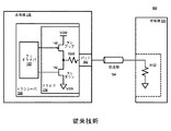
図1Aは、周知のCMOS出力ドライバのブロック図である。周知のCMOS(相補型金属−酸化膜半導体)出力ドライバ134は、I/Oシステムの共通設計である。システム102は、受信機120と通信する送信機110を含む。受信機120が送信機110に対する通信を駆動するとき、送信機110が受信デバイスであると理解されるであろう。このように、送信デバイス及び受信デバイスの役割は、逆転されることができ、出力ドライバ134は、トランシーバ130の一部として示される。しかしながら、本明細書の説明の目的のために、主な焦点は、信号の受信ではなく、信号の送信である。送信機110から受信機120への信号の送信の目的のため、受信機120は、負荷インピーダンスR122として具現化され得る。送信機110は、プルアップ(PU)要素140を介してVDDに伝送線154をプルアップし、プルダウン(PD)要素142を介してVSSに伝送線154をプルダウンすることにより受信するべく、受信機120の伝送線154を駆動する。出力インピーダンスR146は、ドライバ134により見られるようなパッド152及び伝送線154のインピーダンスに典型的に一致される。プリドライバ132は、伝送線154上に信号を出力するべく、ドライバ134に対するシグナリング及び制御を提供する。パッド152は、送信デバイス110を伝送線154にインタフェースで接続する。
FIG. 1A is a block diagram of a known CMOS output driver. The well-known CMOS (complementary metal-oxide semiconductor)
システム102の使用の例は、LPDDR3(低電力デュアルデータレートバージョン3、JEDECにより2012年5月に公開された初期仕様)におけるドライバ用である。システム102は、出力信号を駆動するべく、出力電圧の最大振幅をもたらす。複数のコンポーネントのメモリサブシステム以外のコンポーネントは、出力電圧の最大振幅をもたらすドライバを使用することもできる。出力電圧の最大振幅は、複数のコンポーネント間のI/O(入力/出力)又はインタフェースのために大量の電力を使用する。 An example of the use of the system 102 is for drivers in LPDDR3 (Low Power Dual Data Rate Version 3, an initial specification published in May 2012 by JEDEC). The system 102 provides the maximum amplitude of the output voltage to drive the output signal. Components other than the multi-component memory subsystem may use drivers that provide the maximum amplitude of the output voltage. The maximum amplitude of the output voltage uses a large amount of power for I / O (input / output) or interface between multiple components.
以下の説明は、本発明の複数の実施形態の実装の例示を目的として与えられる図を有する図面の説明を含む。図面は、限定ではなく例示を目的として理解されるべきである。本明細書中で用いられるように、1又は複数の「実施形態」という称呼は、本発明の少なくとも1つの実装に含まれる特定の機能、構造、及び/又は特性の説明として理解されるものである。このように、本明細書に現れる「一実施形態において」又は「代替的な実施形態において」のような表現は、本発明の様々な実施形態及び実装を説明し、同一実施形態を必ずしも全て指すものではない。しかしながら、それらはまた、必ずしも互いに排他的ではない。
後述の通り、電圧レギュレータは、信号送信のために、伝送線インタフェース回路の電圧振幅を制御する。伝送線インタフェース回路は、伝送線を駆動するドライバ又はドライバの一部である。伝送線インタフェース回路は、ロジックハイに応答して伝送線をプルアップするp型ドライバ要素と、ロジックローに応答して伝送線をプルダウンするn型ドライバ要素とを含む相補的なドライバ要素を含む。電圧レギュレータは、複数のドライバ要素の1つと対応する電圧レファレンスとの間に連結され、伝送線インタフェース回路の電圧振幅を減らす。一実施形態において、電圧レギュレータは、伝送線インタフェース回路のプルアップレグ及びプルダウンレグの両方で用いられる。このように、第1電圧レギュレータは、高電圧源(VDD)とプルアップ要素との間に配置されることができ、第2電圧レギュレータは、低電圧源又は接地(VSS)とプルダウン要素との間に配置されることができる。減らされた電圧振幅は、I/O送信のシステム内で用いられる電力の量を減らしつつ、I/O(入力/出力)インタフェース規格に準拠させることができる。 As will be described later, the voltage regulator controls the voltage amplitude of the transmission line interface circuit for signal transmission. The transmission line interface circuit is a driver or a part of the driver that drives the transmission line. The transmission line interface circuit includes complementary driver elements including a p-type driver element that pulls up the transmission line in response to a logic high and an n-type driver element that pulls down the transmission line in response to a logic low. The voltage regulator is coupled between one of the plurality of driver elements and the corresponding voltage reference to reduce the voltage amplitude of the transmission line interface circuit. In one embodiment, the voltage regulator is used in both the pull-up and pull-down legs of the transmission line interface circuit. In this way, the first voltage regulator can be placed between a high voltage source (VDD) and a pull-up element, and the second voltage regulator can be a low voltage source or ground (VSS) and a pull-down element. Can be placed between. The reduced voltage amplitude can be made compliant with I / O (input / output) interface standards while reducing the amount of power used in a system for I / O transmission.
一実施形態において、伝送線インタフェース回路の動作は、実証的なテストの使用によりさらに制御され得る。システムは、特定のデバイスのためのデバイスI/O(入力/出力)の性能パラメータを実証的にテストすることができる。テストシステムを介して実証的にテストすることに基づいて、システムは、インターデバイス通信が行われるシステム又はデバイスに固有の性能パラメータを設定することができる。複数の異なるI/O回路パラメータの複数の異なる設定の各々について、テストシステムは、各I/O回路パラメータの値を設定し、(複数の)パラメータ値での通信をストレステストにかけるためのテストトラフィックを生成し、I/O性能特性のための動作マージンを測定する。回路パラメータは、Vref、Ron、スルーレート、オンダイターミネーション(ODT)、レギュレータ出力電圧及び/又は他のパラメータを含み得る。テストシステムは、動作マージンが最小の閾値に適合し、I/O回路パラメータのうちの少なくとも1つの性能が向上される各I/O回路パラメータの値を決定する探索機能をさらに実行する。一実施形態において、システムは、探索機能に基づいて、I/O回路パラメータのランタイム値を設定する。設定は、テストに基づいて、特定のシステムの特定のコンポーネントについて動的に変更され得る。 In one embodiment, the operation of the transmission line interface circuit may be further controlled through the use of empirical tests. The system can empirically test device I / O (input / output) performance parameters for a particular device. Based on empirical testing through a test system, the system can set performance parameters specific to the system or device in which the inter-device communication takes place. For each of a plurality of different settings of a plurality of different I / O circuit parameters, the test system sets a value for each I / O circuit parameter and tests to subject the communication with the parameter value (s) to a stress test Generate traffic and measure the operational margin for I / O performance characteristics. Circuit parameters may include Vref, Ron, slew rate, on-die termination (ODT), regulator output voltage, and / or other parameters. The test system further performs a search function that determines a value for each I / O circuit parameter that meets a threshold with a minimum operating margin and that improves the performance of at least one of the I / O circuit parameters. In one embodiment, the system sets runtime values for I / O circuit parameters based on a search function. Settings can be changed dynamically for specific components of a specific system based on tests.
一実施形態において、説明されるテストシステム又はテストエンジンは、メモリサブシステム、より具体的には、プラットフォームコンポーネント(例えば、プロセッサ、メモリコントローラ)とメモリデバイスとの間の通信をテストするために用いられ得る。スケジューラ又は同等のロジックを有するメモリコントローラを使用する任意のメモリサブシステムは、テストエンジンの少なくとも1つの実施形態を実証できる。本明細書で参照されるメモリデバイスは、異なるメモリタイプを含むことができる。例えば、メモリサブシステムは、本明細書中で、メモリデバイスの一例として説明されるようにDRAMを一般に使用する。このように、本明細書で説明されるテストエンジンは、DDR3(デュアルデータレートバージョン3、2007年6月27日、JEDEC(Joint Electronic Device Engineering Council)によるオリジナルリリース、現在リリース21)、DDR4(DDRバージョン4、JEDECにより2012年9月に公開された最初の仕様)、LPDDR4(低電力デュアルデータレートバージョン4、本願の出願の時点でJEDECによる開発における仕様)、WIDEIO(本願の出願の時点でJEDECによる開発における仕様)及び/又はその他のような多数のメモリ技術及びそのような仕様の派生又は拡張に基づく技術のいずれかと互換性がある。
In one embodiment, the described test system or test engine is used to test communication between a memory subsystem, more specifically a platform component (eg, processor, memory controller) and a memory device. obtain. Any memory subsystem that uses a memory controller with a scheduler or equivalent logic can demonstrate at least one embodiment of a test engine. The memory devices referred to herein can include different memory types. For example, the memory subsystem generally uses DRAM as described herein as an example of a memory device. Thus, the test engines described herein are DDR3 (dual data rate version 3, June 27, 2007, original release by JEDEC (Joint Electronic Engineering Engineering Council), current release 21), DDR4 (DDR).
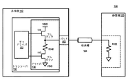
図1Bは、周知のデュアルNMOS出力ドライバのブロック図である。システム104は、図1Aのシステム102と似ているが、n型プルアップ要素144とn型プルダウン要素142とを有する。n型プルアップ要素又はデバイスが要素144をオンにするために必要な閾値電圧を有しており、相補的なドライバ設計よりも出力振幅を減らすので、出力信号の振幅は、システム102におけるよりもシステム104の方が低い。要素110、120、R122、130、132、134、152及び154は、述べた場合を除き、システム104において同一である。出力インピーダンスR148は、典型的には、ドライバ134によって見られるように、パッド152及び伝送線154のインピーダンスと整合するように設計される。
FIG. 1B is a block diagram of a known dual NMOS output driver.
システム104の使用の例は、LPDDR4のドライバについてであり、システム104と同様の設計を提案する。システム104より高い電力を使用するシステム102は、出力信号を駆動するべく、出力電圧の最大振幅をもたらす。しかしながら、システム104は、パッドキャップ(パッド容量)を増加させ、システム102で使用されるものとは異なるスルーレート制御を必要とする。このように、インタフェースシステムは、LPDDR4ドライバに接続される同一のパッド上にレガシーデバイスサポートのためのLPDDR3ドライバを容易に接続できない。さらに、システム104の設計は、PVT(プロセス、電圧及び温度)にわたって十分に制御されないプルアップ電圧及びRon(出力インピーダンス)の値をもたらす。さらに、プルアップ電圧及びRonは、システム104において補償することが困難である。
An example of the use of the
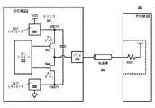
図2は、I/O送信上の振幅を減らす電圧レギュレータを有するシステムの一実施形態のブロック図である。システム200は、ローカルデバイス210を含み、リモートデバイス220と通信する。システム200に関する説明の主な焦点は、ローカルデバイス210からリモートデバイス220への信号の送信に関する。ローカルデバイス210は、送信上で伝送線240を駆動する伝送線インタフェース回路に対して「ローカル」である。このように、デバイス210からデバイス220への送信のために、リモートデバイス220は、伝送線インタフェース回路から離れている。送信機及び受信機としての2つデバイスの役割が逆転され得ると理解されるであろう。デバイス210及び220の送信ドライバ回路は、同一である不要はない。
FIG. 2 is a block diagram of one embodiment of a system having a voltage regulator that reduces the amplitude on the I / O transmission.
ローカルデバイス210は、I/O回路230を含み、パッド212を介して伝送線240とインタフェースで接続される。回路230は、ドライバ232を含み、リモートデバイス220との通信のために、伝送線240を駆動する。一実施形態において、伝送線240は、ローカルデバイス210及びリモートデバイス220のI/Oピンを接続する信号ライン(例えば、トレース)である。伝送線240は、代わりに、有線又は他の相互接続であってよい。
The local device 210 includes an I / O circuit 230 and is connected to the
一実施形態において、ドライバ232は、プルアップ要素及びプルダウン要素と同等の回路を有する、CMOS(相補型金属酸化物半導体)構造である。ドライバ232のプルアップ及びプルダウンレグのいずれか一方又は両方は、電圧レギュレータを介して対応する電圧レファレンスに接続される。一実施形態において、電圧レギュレータは、プルアップレグにおいて提供される。一実施形態において、電圧レギュレータは、プルダウンレグにおいて提供される。一実施形態において、電圧レギュレータは、プルアップ及びプルダウンレグの両方において提供される。例えば、プルアップレグは、電圧レギュレータ(VR)234を介してVDDに接続されることができ、プルダウンレグは、VR236を介してVSSに接続されることができる。このように、ローカルデバイス210による送信のための有効なロジックハイの値は、VDD−VVR234、すなわち、VR234により提供される電圧低下でマイナスされるVDDであり得る。ローカルデバイス210による送信のための有効なロジックローの値は、VSS+VVR236又はVR236により提供される電圧上昇でプラスされるVSSであり得る。VR234及びVR236により提供される電圧変化は、必ずしも同一ではないものと理解されるであろう。両方の場合において、電圧振幅は、電圧レギュレータなしで等価回路から減らされる。
In one embodiment,
出力電圧振幅の減少は、レールからレールへスイングする設計と比較して、回路230に電力節約を提供できる。VR234が回路230に含まれ、VDD−VVR234の出力電圧を提供すると仮定する。VR234がリニア電圧レギュレータである場合、システム200の設計は、VVR234によって提供される電圧低下に対して、線形関係で送信電力を低下する。VR234が、スイッチング電圧レギュレータ又はスイッチ回路レギュレータ(例えば、スイッチドキャパシタレギュレータ、スイッチドインダクタレギュレータ)として設計される場合、システム200の設計は、VVR234によって提供される電圧低下に対して、ほぼ二次関係で送信電力を減らすことができる。一実施形態において、図4及び5に関して詳しく後述される通り、特定のアイ高さ及び/又はアイ幅目標を維持しつつ、総電力を低減するために求めることができるテストシステムからのトレーニングフローを用いることにより、実際の物理デバイスの製造の後に、一方又は両方の電圧レギュレータの正確な振幅のターゲットは、最適化され得る。
The reduction in output voltage amplitude can provide power savings to circuit 230 as compared to a design that swings from rail to rail. Assume that
一実施形態において、一方又は両方の電圧レギュレータ234及び236は、非常に低い面積オーバヘッドで、回路230として、同一の半導体ダイ又は集積回路上にローカルに統合され得る。例えば、デバイス設計は、多くの場合、回路230において電圧レギュレータの実装に適応するための十分な余白を有する。大量のオンダイデカップリングキャパシタンスを要求することなしに、低オーバヘッド電力を実現することができるリニアレギュレータを設計するための周知の技術がある。一実施形態において、電圧レギュレータ234及び236の一方又は両方は、同一の半導体基板上ではなく、回路230として、同一のパッケージ又は同一のボード上に実装される。電圧レギュレータをオフダイとすることは、より高い設計及び/又は実装コストを課すことになり得る。
In one embodiment, one or both
(明示的に示されない)一実施形態において、一方又は両方の電圧レギュレータ234及び236は、バイパス経路を介して選択的にバイパスされ得る。バイパス経路は、電圧レギュレータを通じた電圧レファレンスへの接続又は直接電圧レファレンスへの接続を切り替えるべく、選択的にアクティブにされ得る。このように、例えば、レギュレータへの入力及びレギュレータの出力は、アクティブにされたときに、レギュレータをバイパスする、選択的な(例えば、切替型の)低インピーダンス経路を通じて連結され得る。そのような設計は、複数の異なるタイプのシステムをインタフェースで接続する(例えば、(完全振幅のためにバイパスされる)LPDDR3及び(低振幅のためにレギュレータをアクティブにする)LPDDR4の両方をインタフェースで接続する)のに用いられ得る。さらに、信号の送信を駆動する代わりに信号を受信するような、不要な場合には、電圧レギュレータは、スイッチを切られ得る。このように、低電力状態において、電圧レギュレータは、使用されていないときにドライバに対する電力ゲート及び電力遮断を兼用することができ、回路リークを減らすことができる。
In one embodiment (not explicitly shown), one or both
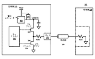
図3Aは、出力信号の高電圧レファレンスに関する振幅を減らすように連結される電圧レギュレータを有するシステムの一実施形態のブロック図である。システム302は、システム200の一実施形態の一例であり得る。送信機310は、ローカルデバイスであり、受信機320は、リモートデバイスである。送信の目的のために、受信機320は、負荷インピーダンスR322としてシステム302に表される。送信機310は、ドライバ334の制御及びシグナリングを提供し、パッド352を介して伝送線354上の出力又は送信信号を駆動するプリドライバ332を含む。
FIG. 3A is a block diagram of one embodiment of a system having a voltage regulator coupled to reduce the amplitude for a high voltage reference of the output signal. System 302 may be an example of one embodiment of
ドライバ334は、プルアップ要素342及びプルダウン要素344を含む。要素344は、ロジックロー信号を生成するべく、伝送線354をプルダウンするn型(例えば、NMOS)要素である。要素342は、ロジックハイ信号を生成するべく、伝送線354をプルアップするp型(例えば、PMOS)要素である。「ロジックロー」及び「ロジックハイ」は、電圧レベルを指し、デバイス310及び320間で用いられる通信プロトコル又はシグナリングではないと理解されるであろう。例えば、あるシグナリングスキームにおいて、ロジックローは、「0(ゼロ)」を送信することに対応でき、ロジックハイは、「1」を送信することに対応できる。しかしながら、シグナリングスキームは、反転されてよく、ロジックハイが0(ゼロ)を送信することに対応でき、ロジックローが1を送信することに対応できる。
送信機310は、VDDからVDDTXへの送信高電圧レベルをより低くする電圧レギュレータ362を含み、VDDTXは、VDDから電圧レギュレータ362の電圧降下を引いたものである。一実施形態において、送信機310は、電圧レギュレータ362をバイパスすることを可能にするバイパス経路372を含む。平滑コンデンサは、電圧レギュレータ362により導入され得るノイズをフィルタするべく、VDDTXからVSSへ配置され得る。ドライバ334は、相補的な出力要素342及び344とパッド352との間で連結される出力インピーダンス、Ron、R346を含む。システム302の設計は、十分に制御されたRon及び出力電圧レベルを提供する。さらに、出力電圧レベルは、電圧レギュレータ362の出力を調整することにより、調整可能であり得る。
Transmitter 310 includes a voltage regulator 362 that lowers the transmission high voltage level from VDD to VDDTX, which is VDD minus the voltage drop of voltage regulator 362. In one embodiment, the transmitter 310 includes a
システム302は、LPDDR4低振幅VSS終端スキームの実装として用いられ得る。さらに、システム302は、例えば、電圧レギュレータ362を選択的にバイパスすることにより、LPDDR3及びLPDDR4の両方を実装し得る。このように、システム302は、高性能な組み合わせLPDDR3/4設計をサポートする。一実施形態において、バイパス経路372は、電圧レギュレータ362の一部であり、又は、電圧レギュレータ362により実装され、レギュレータにVDDからVDDTXを短絡させることを可能にする。当業者は、システム302の設計がパッドキャップ又は送信機310の全体的な性能に影響を与えないことを理解するであろう。
System 302 can be used as an implementation of the LPDDR4 low amplitude VSS termination scheme. Further, system 302 may implement both LPDDR3 and LPDDR4, for example, by selectively bypassing voltage regulator 362. Thus, the system 302 supports a high performance combined LPDDR3 / 4 design. In one embodiment,
CMOSバッファの使用は、Ronの一定のインピーダンスをパッド352に与えることにより、固有の信号インテグリティの利益を提供する。このように、送信機310は、伝送線354の特性インピーダンスに適合させ、反射に起因する任意の過剰なエネルギーを緩和することができる。しかしながら、電圧レギュレータ362のターゲット電圧を調整することにより、システム302は、所望の振幅又は共通モード電圧を実現するべく、受信機320に提示される振幅を調整できる。結果として、システム302は、I/Oバッファ振幅及びRonに対する独立制御を提供する。
The use of a CMOS buffer provides inherent signal integrity benefits by providing a constant impedance of Ron to pad 352. In this way, transmitter 310 can adapt to the characteristic impedance of
図3Bは、出力信号の低電圧レファレンスに関する振幅を減らすように連結される電圧レギュレータを有するシステムの一実施形態のブロック図である。システム304は、システム200の一実施形態の一例であり得る。送信機310は、ローカルデバイスであり、受信機320は、リモートデバイスである。送信の目的のために、受信機320は、負荷インピーダンスR322としてシステム304内で表され、特定の実施態様により、VDD、共通モード電圧又は接地に終端できる。送信機310は、ドライバ334のための制御及びシグナリングを提供し、パッド352を介して伝送線354上の出力又は送信信号を駆動するプリドライバ332を含む。ドライバ334は、プルアップ要素342及びプルダウン要素344を含む。要素344は、ロジックロー信号を生成するべく、伝送線354をプルダウンするn型(例えば、NMOS)要素である。要素342は、ロジックハイ信号を生成するべく、伝送線354をプルアップするp型(例えば、PMOS)要素である。
FIG. 3B is a block diagram of one embodiment of a system having a voltage regulator coupled to reduce amplitude for a low voltage reference of the output signal.
送信機310は、送信低電圧レベルをVSSからVSSTXへ引き上げる電圧レギュレータ364を含み、VSSTXは、VSSに電圧レギュレータ364の電圧をプラスしたものである。一実施形態において、送信機310は、電圧レギュレータ364をバイパスすることを可能とするバイパス経路374を含む。平滑コンデンサは、電圧レギュレータ364により導入され得るノイズをフィルタするべく、VSSTXからVSS(又は、環境に依存してVDD)に配置される。ドライバ334は、相補的な出力要素342及び344とパッド352との間に連結される出力インピーダンス、Ron、R346を含む。システム304の設計は、十分に制御されたRon及び出力電圧レベルを提供する。さらに、出力電圧レベルは、電圧レギュレータ364の出力を調整することにより調整可能となり得る。
The transmitter 310 includes a voltage regulator 364 that raises the transmission low voltage level from VSS to VSSTX, where VSSTX is the voltage of the voltage regulator 364 plus VSS. In one embodiment, the transmitter 310 includes a
図3Cは、出力信号の低電圧レファレンス及び高電圧レファレンスの両方に関する振幅を減らすように連結される電圧レギュレータを有するシステムの一実施形態のブロック図である。システム306は、システム200の一実施形態の一例であり得る。送信機310は、ローカルデバイスであり、受信機320は、リモートデバイスである。送信の目的のために、受信機320は、負荷インピーダンスR322としてシステム306において表され、共通モード電圧又はVDDに終端できる。送信機310は、ドライバ334の制御及びシグナリングを提供し、パッド352を介して伝送線354上の出力又は送信信号を駆動するプリドライバ332を含む。ドライバ334は、プルアップ要素342及びプルダウン要素344を含む。要素344は、ロジックロー信号を生成するべく、伝送線354をプルダウンするn型(例えば、NMOS)要素である。要素342は、ロジックハイ信号を生成するべく、伝送線354をプルアップするp型(例えば、PMOS)要素である。
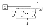
FIG. 3C is a block diagram of one embodiment of a system having a voltage regulator coupled to reduce the amplitude for both the low voltage reference and the high voltage reference of the output signal. System 306 may be an example of an embodiment of
送信機310は、VDDからVDDTXに送信高電圧レベルをより低くする電圧レギュレータ366を含み、VDDTXは、VDDから電圧レギュレータ366の電圧降下をマイナスしたものである。一実施形態において、送信機310は、電圧レギュレータ366をバイパスするバイパス経路(明示的に示されない)を含む。送信機310は、送信低電圧レベルをVSSからVSSTXに引き上げる電圧レギュレータ368も含み、VSSTXは、VSSに電圧レギュレータ368の電圧をプラスしたものである。一実施形態において、送信機310は、電圧レギュレータ368をバイパスするバイパス経路を含む(明示的に示されない)。キャパシタは、出力信号のノイズをフィルタするべく、VDDTXからVSSTXの間に配置され得る。ドライバ334は、出力インピーダンスを含むように明示的に示されていないが、出力インピーダンスが提供され得る。ドライバ334の出力電圧レベルは、高電圧及び低電圧の両方に関して調整され得る。
Transmitter 310 includes a voltage regulator 366 that lowers the transmission high voltage level from VDD to VDDTX, where VDDTX is the voltage drop across voltage regulator 366 from VDD. In one embodiment, transmitter 310 includes a bypass path (not explicitly shown) that bypasses voltage regulator 366. The transmitter 310 also includes a voltage regulator 368 that raises the transmission low voltage level from VSS to VSSTX, which is VSS plus the voltage of the voltage regulator 368. In one embodiment, transmitter 310 includes a bypass path that bypasses voltage regulator 368 (not explicitly shown). A capacitor can be placed between VDDTX and VSSTX to filter noise in the output signal. Although
システム306は、LPDDR3出力ドライバと同様にWIDEIO出力ドライバの実装として用いられることができ、振幅がVDD/2を基準にする任意のI/Oに適用可能である。WIDEIOを用いて、周知の設計は、パッド352を全レール(VSSからVDD)にスイング(swing)する。LPDDR3を用いて、受信機は、VDD/2の共通モードを予測する。ドライバは、CV2F(ここで、Cはキャパシタンスであり、Vは電圧であり、Fは信号の周波数である)に等しい電力を消費する。JEDECによる規格は、LPDDR3についての仕様及びWIDEIOについての提案された仕様のように、必要な許容範囲内である、およそ0.2*VDDから0.8*VDDまでのパッド振幅(pad swing)を可能にする。しかしながら、周知の設計は、完全なレールをスイングする。電圧レギュレータ366及び368がVDDの20%に設定された場合、0からVDDまでスイングするのと比較して40%の電力消費量を減らしつつ、出力振幅は、さらに規格に準拠する。あるいは、電圧レギュレータ366及び368は、異なる値に設定されることができるが、必ずしも等しい電圧ステップに設定される必要はない。電圧レギュレータ366及び368が受信機320についてVDD/2の共通モードを維持するべく、対称的に動作する(例えば、等しい量で電圧振幅を調整する)ように構成され得ると理解されるであろう。
The system 306 can be used as a WIDEIO output driver implementation, similar to the LPDDR3 output driver, and is applicable to any I / O whose amplitude is referenced to VDD / 2. Using WIDEIO, known designs swing the
WIDEIOの実装において、受信回路は、一般に、シンプルなインバータとして実装される。このように、リーク電力消費は、パッド352が完全なレールをスイングしないときに、飛躍的に向上する。アイドル期間の間、パッド352を電圧レファレンスレール(VDD又はVSS)に引っ張るバイパス経路の使用は、リーク電力消費を減らすことができる。CV2F電力が影響を及ぼす高アクティビティ期間の間、システム306は、省電力化するべく、出力電圧振幅を落とすように調整できる。リーク電力が影響を及ぼすアイドル期間の間、システム306は、パッド352を完全なレールでスイングさせるように、電圧レギュレータをバイパスして、リークを減らす又は取り除く。一実施形態において、バイパス経路は、アイドル期間の間、パッド352をVDD/VSSに引き寄せる弱プルアップ/プルダウンパスとして実装され得る。概して、バイパス経路は、電圧レギュレータオフセットを有する代わりに送信電圧を基準電圧に等しくする低インピーダンスパス、又は、高インピーダンスパス(例えば、電力ゲート)のいずれかとして実装され得る。
In the implementation of WIDEIO, the receiving circuit is generally implemented as a simple inverter. Thus, leakage power consumption is dramatically improved when the
図3A、3B又は3Cのいずれか任意の実施形態において、テストシステムは、(例えば、デバイスインフィールドの動作を調整する)特定の製造デバイスに基づいて出力電圧振幅をプログラムするようにさらに追加され得る。このように、VSSTX及び/又はVDDTxの正確なターゲット値は、電力のアイ高さ及び/又はアイ幅の評価に基づいて、テストシステムにより調整され得る。VSSTX及びVDDTXの非対称値は、さらに電力を減らししつつ、システムにハイ側及びロー側電圧マージンを等しくさせることが可能となり得る。そのような技術は、さらに後述される。 In any embodiment of any of FIGS. 3A, 3B, or 3C, a test system may be further added to program the output voltage amplitude based on a particular manufacturing device (eg, adjusting device in-field operation). . Thus, the exact target value of VSSTX and / or VDDTx can be adjusted by the test system based on the evaluation of power eye height and / or eye width. Asymmetric values of VSSTX and VDDTX may allow the system to equalize the high and low side voltage margins while further reducing power. Such techniques are further described below.
図4は、出力電圧振幅を制御するべく、テストインシステムを提供するテストシステムを有するメモリサブシステムの一実施形態のブロック図である。特定の出力電圧振幅は、アイ高さ及び/又はアイ幅と総電力との間のトレードオフを決定するべく、動作中の特定のデバイスのために算出され得る。メモリサブシステム400が具体的に示される一方、インターデバイス通信を利用する他の電子デバイスサブシステムが等しく用いられ得ると理解されるであろう。メモリサブシステム400は、メモリデバイス410、テストシステム420、パラメータ調整ロジック430、測定ロジック440及び探索ロジック450を含むことができる。そのような機能的なロジックは、ハードウェア、ソフトウェア、ファームウェア又は組み合わせを指す。機能的なロジックはまた、SoC(システムオンチップ)内に直接的に実装されることができ、又は離れて設けられて別のI/Oインタフェースを介して通信できる。
FIG. 4 is a block diagram of one embodiment of a memory subsystem having a test system that provides a test-in system to control output voltage amplitude. A particular output voltage amplitude may be calculated for a particular device in operation to determine a trade-off between eye height and / or eye width and total power. While the memory subsystem 400 is specifically shown, it will be understood that other electronic device subsystems that utilize inter-device communication can equally be used. The memory subsystem 400 can include a memory device 410, a test system 420, parameter adjustment logic 430, measurement logic 440, and
メモリデバイス410は、メモリサブシステムにおける1又は複数のストレージデバイスを表す。テストシステム420は、メモリデバイス410と通信することに関して、どのようにI/O動作パラメータを設定するかを決定するべく、メモリデバイス410と通信のテストを提供する。他のI/O動作パラメータの間で、テストシステム420は、特定のメモリデバイス410(又は、送信デバイスから他の受信デバイス)に対する出力の電圧振幅を減らするべく、特定の電圧レギュレータ設定を決定できる。一実施形態において、テストシステム420は、テストを実行するループを表すテストループ422を含む。特に、一実施形態において、テスト及び測定は、どのようにメモリデバイス410が様々な条件の下で実行するかを決定するべく、ループ422において反復的に実行される。一実施形態において、テストシステム420は、異なるパラメータ設定について多数の測定に基づいて、メモリデバイス410の性能(例えば、最悪の場合の性能)を推定するために用いられる推定ロジック(明示的に示されない)を含む。一実施形態において、テストシステム420は、テスト結果において、ノイズを減らす又は補償するべく複数のテスト結果を互いに関連付けるのに用いられる相関ロジック(具体的に示されない)を含む。 Memory device 410 represents one or more storage devices in the memory subsystem. Test system 420 provides a test of communication with memory device 410 to determine how to set I / O operating parameters in connection with communicating with memory device 410. Among other I / O operating parameters, test system 420 can determine specific voltage regulator settings to reduce the voltage swing of the output for a particular memory device 410 (or other receiving device to other receiving device). . In one embodiment, test system 420 includes a test loop 422 that represents a loop that performs the test. In particular, in one embodiment, tests and measurements are performed iteratively in loop 422 to determine how the memory device 410 performs under various conditions. In one embodiment, the test system 420 uses estimation logic (not explicitly shown) that is used to estimate the performance (eg, worst case performance) of the memory device 410 based on multiple measurements for different parameter settings. )including. In one embodiment, test system 420 includes correlation logic (not specifically shown) that is used to correlate multiple test results with each other to reduce or compensate for noise in the test results.
パラメータ調整ロジック430は、性能パラメータを変更するロジックを表す。一実施形態において、ロジック430は、電圧レギュレータ値を調整する、又はメモリデバイス410に対する電圧レファレンスを調整するロジックを表す。電圧レギュレータは、制御ロジックに応答して出力電圧振幅を調整するべく、可変電圧を提供する可変出力回路を含み得る。一実施形態において、ロジック430は、1又は複数のレイテンシパラメータを調整するロジックを表す。例えば、ロジック430は、Ron(出力インピーダンス)、Rodt(オンダイターミネーションインピーダンス)、スルーレート、等化、データストローブ間に集中するタイミング、周波数、又は、他の電気パラメータのような電気パラメータを調整し得る。一実施形態において、ロジック430は、1又は複数の周波数パラメータを調整するロジックを表す。例えば、ロジック430は、上記の任意のレイテンシパラメータ又は他のタイミングパラメータ、ターンアラウンドタイム又は他のI/Oパラメータに関連するパラメータを調整し得る。レイテンシ及び/又は周波数は、電圧レギュレータの設定に影響を与え得る。 The parameter adjustment logic 430 represents logic for changing performance parameters. In one embodiment, logic 430 represents logic that adjusts a voltage regulator value or adjusts a voltage reference for memory device 410. The voltage regulator may include a variable output circuit that provides a variable voltage to adjust the output voltage amplitude in response to the control logic. In one embodiment, logic 430 represents logic that adjusts one or more latency parameters. For example, logic 430 may adjust electrical parameters such as Ron (output impedance), Rodt (on-die termination impedance), slew rate, equalization, timing concentrated between data strobes, frequency, or other electrical parameters. . In one embodiment, logic 430 represents logic that adjusts one or more frequency parameters. For example, the logic 430 may adjust parameters related to any of the above latency parameters or other timing parameters, turnaround times or other I / O parameters. Latency and / or frequency can affect the setting of the voltage regulator.
一実施形態において、パラメータ調整ロジック430は、メモリコントローラの一部であり、遅延を制御するメモリコントローラ内の構成設定に影響を与える。一実施形態において、ロジック430は、メモリコントローラの近くのテストエンジンのような、メモリコントローラの外側に存在する。一実施形態において、ロジック430は、設定オプションを設定することによるといったように、メモリコントローラにメモリデバイス自身における設定を調整させる。一実施形態において、パラメータ調整ロジック430は、メモリサブシステムが動作する周波数を細かい粒度ステップサイズで調整できる。テストシステム420は、テストに基づいて、メモリサブシステム400に固有の動作設定を決定する。メモリサブシステム400において、出力ドライバは、メモリコントローラ内に存在し、本明細書に記載された任意の実施形態に従って電圧振幅を調整する(複数の)電圧レギュレータを含む。 In one embodiment, the parameter adjustment logic 430 is part of the memory controller and affects configuration settings within the memory controller that control the delay. In one embodiment, logic 430 resides outside the memory controller, such as a test engine near the memory controller. In one embodiment, logic 430 causes the memory controller to adjust settings on the memory device itself, such as by setting configuration options. In one embodiment, the parameter adjustment logic 430 can adjust the frequency at which the memory subsystem operates at a fine granularity step size. The test system 420 determines operational settings specific to the memory subsystem 400 based on the test. In the memory subsystem 400, the output driver is present in the memory controller and includes voltage regulator (s) that adjust the voltage amplitude according to any of the embodiments described herein.
測定ロジック440は、性能の1又は複数の指標を測定するロジックを表す。例えば、ロジック440は、信号のアイ幅、信号のアイ高さ又は両方を測定できる。一実施形態において、ロジック440は、0度又は90度以外の角度で測定することにより、アイ高さ/アイ幅の2次元バージョンを測定する。一実施形態において、ロジック440は、メモリサブシステム400による電力消費を測定する。設定は、測定ロジック440の測定の粒度に従ってパラメータ調整ロジック430により調整される(すなわち、検出可能な違いを生じるのに十分なパラメータ設定を変更する)と理解されるであろう。探索ロジック450は、メモリデバイス410のI/Oにどの設定を使用するかを測定値から決定するロジックを表す。一実施形態において、測定ロジック440は、テスト対象の特定のメモリサブシステム400について、1又は複数の代表的な性能曲線を生成するために用いられる。代表的な曲線に基づいて、探索ロジック450は、他のために(基準又は設定により)必要な性能を少なくとも維持しつつ、少なくとも1つパラメータについて、より良好な性能を満たすために、どの設定を使用するかを決定するべく、探索機能を実行できる。探索ロジック450は、n次元探索ロジック、(n1次元探索を実行する)1次元探索ロジック、線形適合探索ロジック、二次適合探索ロジック、最急降下探索ロジック、曲線適合探索ロジック又はその他を含むことができる。nは、探索するための独立パラメータの数を示す整数を表すと理解されるであろう。探索ロジック450は、再現性ノイズを減らすこと又は最悪の場合の条件を推定することのいずれかと一緒に、複数の測定を組み合わせることもできる。一実施形態において、管理者は、どの判断(I/O電力、I/O周波数又はI/Oレイテンシ)がメモリサブシステム400のシステム配備にとって最も顕著な特性であるかを決定し、その特定のターゲット特性を改善するテスト動作を行うことができる。
Measurement logic 440 represents logic for measuring one or more indicators of performance. For example, the logic 440 can measure the eye width of the signal, the eye height of the signal, or both. In one embodiment, logic 440 measures a two-dimensional version of eye height / eye width by measuring at an angle other than 0 or 90 degrees. In one embodiment, logic 440 measures power consumption by memory subsystem 400. It will be appreciated that the settings are adjusted by the parameter adjustment logic 430 according to the measurement granularity of the measurement logic 440 (ie, changing parameter settings sufficient to produce a detectable difference).
I/O電力は、デバイス間の通信を送るのに用いられる電力を指し、多くの電子デバイスにおける電力消費のかなりの量を占める。I/Oレイテンシは、アクセストランザクションのために、メモリデバイスにアクセスするのに要する時間に影響を与える。より低いI/Oレイテンシは、より速いアクセスをもたらすことができ、このため、より速いデータの取得に起因してシステムの性能を向上させる。I/O周波数は、アクセストランザクションのために、メモリデバイスにアクセスするのに要する時間に影響を与える。より高いI/O周波数は、より高い帯域幅をもたらすことができ、このため、より速いデータの取得に起因してシステムの性能を向上させる。より高い帯域幅は、所与の期間内により多くの動作を可能とし、データにより制限されるシステムがより高い性能で動作することを可能とすることができる。I/Oがアクティブである時間を減少させ、I/Oが低電力状態である時間を増大させることにより、電力を減らすこともできる。 I / O power refers to the power used to send communications between devices and accounts for a significant amount of power consumption in many electronic devices. I / O latency affects the time required to access a memory device due to an access transaction. Lower I / O latency can result in faster access, thus improving system performance due to faster data acquisition. The I / O frequency affects the time required to access the memory device for access transactions. Higher I / O frequencies can result in higher bandwidth, thus improving system performance due to faster data acquisition. Higher bandwidth may allow more operation within a given period and allow a data limited system to operate with higher performance. Power can also be reduced by reducing the time that I / O is active and increasing the time that I / O is in a low power state.
現在、I/O電力、I/Oレイテンシ及びI/O周波数に関するデバイスの性能は、特定のDPM(defect per million)レベルにおける機能を保証する固定値設定により制御されているが、個々の、特定のデバイスについて、最低限可能な動作I/Oレイテンシを実現しない。一実施形態において、本明細書中で説明されるように、テストシステムは、DPM目標をさらに維持しつつ、特定のデバイスについて動作電力、レイテンシ及び/又は周波数を設定できる設定を実証的にテスト及び決定する。各設定は、電圧レギュレータが低減された出力振幅を提供するために設定すべきレベルにより影響を与え又は影響を受ける。テストシステム420は、通信の異なるメトリックについて所望の性能を実現しつつ、どの設定を電圧レギュレータに使用するかを実証的にテストする。 Currently, device performance with respect to I / O power, I / O latency, and I / O frequency is controlled by fixed value settings that guarantee functionality at a specific DPM (defect per million) level, but individual, specific The minimum possible operation I / O latency is not realized for these devices. In one embodiment, as described herein, the test system empirically tests and configures settings that can set operating power, latency, and / or frequency for a particular device while further maintaining DPM targets. decide. Each setting is influenced or affected by the level that the voltage regulator should set to provide a reduced output amplitude. Test system 420 empirically tests which setting is used for the voltage regulator while achieving the desired performance for different metrics of communication.
任意のターゲットI/O性能特性(例えば、I/O電力、I/Oレイテンシ、I/O周波数)について、テストシステムは、ターゲット性能特性に影響を与える任意の数のI/O回路パラメータを調整できる。テストシステムは、例えば、PLL(phase locked loop(位相ロックループ))回路における分数−N分周器を用いることにより周波数を調整でき、分数−N分周器は、全体として、コンピューティングデバイスの代わりに、メモリサブシステムの周波数のみを調整できる。メモリサブシステム周波数を調整する他の方法はまた、オーバークロックシステムの当業者により理解されるであろう。テストシステムは、次に、各設定にわたって1又は複数の動作マージン(例えば、タイミング、最大周波数及び/又は電圧)を測定する。テストシステムは、ターゲット性能特性の性能を改善しつつ、最小限の要件(例えば、デバイスにDPM要件を満たすことを可能とする設定)を維持する設定を識別するべく、測定値に基づいて探索を実行する。テストシステムの動作は、システムを「最適化する」と言える。「最適化する」とは、必ずしも絶対的に可能な最良な性能を指すものでないと理解されるであろう。代わりに、最適化することは、特定の条件に関する、若しくは、特定の環境における若しくは特定の制約内における性能を改善すること、又は、最大化することの指すことができる。 For any target I / O performance characteristic (eg, I / O power, I / O latency, I / O frequency), the test system adjusts any number of I / O circuit parameters that affect the target performance characteristic it can. The test system can adjust the frequency by using, for example, a fractional-N divider in a PLL (phase locked loop) circuit, the fractional-N divider as a whole instead of a computing device. In addition, only the frequency of the memory subsystem can be adjusted. Other methods of adjusting the memory subsystem frequency will also be understood by those skilled in the art of overclocking systems. The test system then measures one or more operating margins (eg, timing, maximum frequency and / or voltage) across each setting. The test system searches based on measurements to identify settings that maintain the minimum requirements (eg, settings that allow the device to meet DPM requirements) while improving the performance of the target performance characteristics. Run. The operation of the test system can be said to "optimize" the system. It will be understood that “optimizing” does not necessarily refer to the best possible performance. Instead, optimizing can refer to improving or maximizing performance with respect to specific conditions or in specific environments or within specific constraints.
上記の例により提供されるように、テストは、関心のある1又は複数の性能パラメータの観点からメモリデバイスにストレスを与える。他の性能パラメータは、テストシステムにより評価され得ると理解されるであろう。ある観点から、メモリデバイス及びメモリサブシステム(又は他のサブシステム)は、I/Oに関するメモリサブシステム及びメモリデバイスに適用可能な仕様又は規格を超えてサブシステムが動作され得るか否かを決定するべく、具体的にテストされたインシステムである。テストは、外部の試験機器を必要とせずに、システムそれ自体のみに基づいて実行され得る。 As provided by the above example, testing stresses the memory device in terms of one or more performance parameters of interest. It will be appreciated that other performance parameters may be evaluated by the test system. From one perspective, the memory device and memory subsystem (or other subsystem) determines whether the subsystem can be operated beyond specifications or standards applicable to the memory subsystem and memory device for I / O. In-system specifically tested to do. The test can be performed based solely on the system itself, without the need for external test equipment.
テストに関して、本明細書で言及されるようなテストシステムは、(例えば、共有ダイスペース上、SoC(システムオンチップ)上の)メモリコントローラに及び/又はメモリコントローラの近くに位置付けられるハードウェア要素、又は、そのI/O性能が、出力振幅を減らすために電圧レギュレータで制御されるべき他のターゲットデバイスを含む。テストシステムは、I/Oに誘発された電源ノイズ、符号間干渉(ISI(inter−symbol interference))、信号クロストーク及び/又は他の条件をもたらすI/O(入力/出力)の正確な組み合わせを作成する。これらの効果のいずれかは、各I/Oレーン上のデータ、各コマンドレーン上のパターン、及び/又は、どのようにデータ信号が複数のレーンにわたって互いに位置合されるかを正確に制御することにより作成され得る。 With respect to testing, a test system as referred to herein may include hardware elements located at and / or near a memory controller (eg, on a shared die space, on a SoC (system on chip)), Alternatively, its I / O performance includes other target devices that are to be controlled by a voltage regulator to reduce output amplitude. The test system is an accurate combination of I / O (input / output) that results in I / O induced power noise, inter-symbol interference (ISI), signal crosstalk and / or other conditions. Create Any of these effects can precisely control the data on each I / O lane, the pattern on each command lane, and / or how the data signals are aligned with each other across multiple lanes. Can be created.
図5は、信号振幅を制御する電圧レギュレーションを有するメモリコントローラ及びメモリデバイス通信サブシステムの一実施形態のブロック図である。一実施形態において、システム500は、メモリコントローラ530及びメモリデバイス550を含むメモリサブシステムを有する。システム500は、製造システム又はメモリデバイス550が消費者によって用いられるように配置されるシステムを表す。システム500は、ホストプロセッサ502が存在するハードウェアプラットフォーム(明示的には示されない)と、メモリコントローラ530及びメモリデバイス550を含むメモリサブシステムとを含む。BIOS(基本入出力システム)520又はメモリサブシステムを含むシステムを初期化するための等価ファームウェアもまた、ハードウェアプラットフォーム上に存在する。
FIG. 5 is a block diagram of one embodiment of a memory controller and memory device communication subsystem having voltage regulation to control signal amplitude. In one embodiment, the system 500 has a memory subsystem that includes a memory controller 530 and a memory device 550. System 500 represents a manufacturing system or system in which memory device 550 is arranged for use by a consumer. System 500 includes a hardware platform (not explicitly shown) in which
ホストプロセッサ502は、特に、ホストオペレーティングシステム(OS)510を実行するものである。ホストOS510は、一般に、ランタイム中のシステム500の動作制御を提供する。ホストOS510は、システム500とインタラクションすることをユーザに可能にするべく、ソフトウェアをハードウェアに、及び、ハードウェアをソフトウェアに接続するインタフェースに提供する。BIOS520は、ホストOS510がロードされるまで、システム500を介して起動制御を提供する。
The
ホストOS510は、データの読み出し及び/又は書き込みのために、メモリデバイス550へのアクセスのためのメモリアクセス要求をメモリコントローラ530に提供する。同様に、BIOS520は、メモリアクセス要求をメモリコントローラ530に提供できる。メモリコントローラ530は、データアクセス要求に応答してメモリデバイス550にアクセスする。一実施形態において、テストエンジン540は、メモリデバイス550へ送るべく、メモリコントローラ530へのデータアクセス要求及び/又はアクセストランザクションを生成する。一実施形態において、テストエンジン540は、テストデータをメモリデバイス550へ直接提供する。 The host OS 510 provides a memory access request for accessing the memory device 550 to the memory controller 530 for reading and / or writing data. Similarly, the BIOS 520 can provide memory access requests to the memory controller 530. The memory controller 530 accesses the memory device 550 in response to the data access request. In one embodiment, test engine 540 generates a data access request and / or access transaction to memory controller 530 to send to memory device 550. In one embodiment, test engine 540 provides test data directly to memory device 550.
一実施形態において、BIOS520は、テストプログラム522を介してテストを開始し、メモリコントローラ530を介したメモリデバイス550との通信をテストするべく、テストデータ542を生成するテストエンジン540にアクセスする。一実施形態において、テストデータ542は、異なるパラメータ設定の下でメモリデバイス550の性能を識別することに用いられるデータのような、メモリデバイス550のテストを監視している間に格納されたデータを表す。メモリデバイスの性能を識別することに応答して、システム500は、メモリデバイス550のI/Oのための動作パラメータを動的に設定できる。動作パラメータを動的に設定することは、全てのデバイスに一般に適用可能な基準の又はデフォルトの設定を用いるのではなく、特定のデバイスに従ってシステムに性能を設定させることを可能にする。このように、特定のシステムは、最悪の場合に想定されるシステムの性能に限定されない。
In one embodiment, the BIOS 520 initiates a test via the test program 522 and accesses a test engine 540 that generates
一実施形態において、設定552は、TX/RX554のI/O設定を格納するレジスタ又は他の設定メカニズムのようなメモリデバイス550内のメカニズムを表す。TX/RX554は、メモリデバイス550のI/O性能を制御するメモリデバイス550の送受信回路を表す。VR536は、TX/RX554の出力振幅を制御するのに用いられる1又は複数の電圧レギュレータを表す。一実施形態において、設定532は、TX/RX534のI/O設定を格納するメモリコントローラ530におけるメカニズムを表す。TX/RX534は、メモリデバイス550に対するI/O性能を制御するメモリコントローラ530の送受信回路を表す。設定532は、TX/RX534の出力振幅を調整するべく、VR536の設定を格納することもできる。他のコンポーネントは、TX/RX回路を介してメモリデバイス550に接続されることもでき、同様の設定メカニズムを有すると理解されるであろう。
In one embodiment, settings 552 represent a mechanism within memory device 550, such as a register or other configuration mechanism that stores TX / RX 554 I / O settings. TX / RX 554 represents a transmission / reception circuit of the memory device 550 that controls the I / O performance of the memory device 550. VR536 represents one or more voltage regulators used to control the output amplitude of TX / RX554. In one embodiment, settings 532 represent a mechanism in memory controller 530 that stores TX / RX 534 I / O settings. TX /
設定532及び522は、送受信機能のための設定を含むことができる。例えば、様々な設定は、タイミング、電力、出力電圧レベル、電圧レギュレータレベル、出力インピーダンス、スルーレート又は他の送信パラメータを制御することに適用され得る。受信側において、オンダイターミネーション(ODT)、増幅器利得、等化及び他の受信機パラメータは、様々な設定により制御され得る。テストエンジン540は、送受信パラメータの様々な異なる設定でテストを実行し、測定結果を作成し、システムの動作マージン(例えば、必要な最小限の性能と比較して、どのようにシステムが実行するか)を決定することができる。動作マージンは、例えば、様々な性能特性について最小の閾値(一実施形態においてガードバンドを含む)を有することにより決定され得る。このように、動作マージンを決定することは、閾値と比較して実際の性能を決定することを含む。閾値は、異なる動作電圧、温度又はテストにおける複数の測定に基づいて動的に計算され、最悪の場合の条件に対して推定し得る。さらに、1又は複数の閾値は、テストされる異なる動作マージンのそれぞれについて異なり得る。 Settings 532 and 522 may include settings for transmission and reception functions. For example, various settings may be applied to control timing, power, output voltage level, voltage regulator level, output impedance, slew rate, or other transmission parameters. On the receiver side, on-die termination (ODT), amplifier gain, equalization and other receiver parameters can be controlled by various settings. The test engine 540 performs tests with various different settings of transmit and receive parameters, creates measurement results, and how the system performs compared to the operating margin of the system (eg, compared to the minimum required performance). ) Can be determined. The operating margin can be determined, for example, by having minimum thresholds (including guard bands in one embodiment) for various performance characteristics. Thus, determining the operating margin includes determining actual performance relative to a threshold value. The threshold is calculated dynamically based on different measurements at different operating voltages, temperatures or tests and can be estimated for worst case conditions. Further, the one or more thresholds may be different for each of the different operating margins tested.
一実施形態において、システム500は、設定532及び522が、I/O電力の使用に影響を与えるI/O回路パラメータを変更するための機能を少なくとも含む場合において、I/O電力を減らすように構成される。パラメータの例では、限定はされないが、終端値、バイアス、スルーレート、ドライバ振幅、ドライバインピーダンス及び(VR536の設定を含む)動作電圧を含む。そのような実施形態において、テストエンジン540は、最悪の場合の刺激(stimulus)に対して周知の相関関係があるもののI/Oを刺激(stimulate)するテストコンテンツを生成する。テストエンジン540は、様々な回路設定について、動作電圧及び/又はタイミングマージンを測定する。テストエンジン540は、次に、測定された回路パラメータマージンデータを(例えば、本明細書中で説明されるような探索機能により)分析し、テストされ及び測定されたパラメータ及び設定について規定された製品のDPM要件をさらに維持する最も低い動作I/O電力を決定する。 In one embodiment, the system 500 reduces I / O power when the settings 532 and 522 include at least functionality for changing I / O circuit parameters that affect the use of I / O power. Composed. Examples of parameters include, but are not limited to, termination value, bias, slew rate, driver amplitude, driver impedance, and operating voltage (including VR536 settings). In such an embodiment, the test engine 540 generates test content that stimulates I / O with a well-known correlation to worst-case stimuli. Test engine 540 measures operating voltage and / or timing margin for various circuit settings. The test engine 540 then analyzes the measured circuit parameter margin data (eg, with a search function as described herein) and defines the tested and measured parameters and settings as defined. The lowest operating I / O power that further maintains the DPM requirements of
一実施形態において、システム500は、設定532及び522が、I/O周波数に影響を与えるI/O回路パラメータを変更するための機能を少なくとも含む場合において、I/O周波数が高まるように構成される。パラメータの例では、限定はされないが、終端値、バイアス、スルーレート、電流モードドライバ及び(VR536の設定を含む)動作電圧を含む。周波数パラメータは、限定はされないが、DLL(delay locked loops(遅延ロックループ))、PLL(phase locked loops(位相ロックループ))及び/又はクロックチップを含むことができるコンポーネントにより影響を受け得る。そのような実施形態において、テストエンジン540は、最悪の場合の刺激に対して周知の相関関係があるもののI/Oを刺激するテストコンテンツを生成する。テストエンジン540は、様々な回路設定について、動作電圧、動作周波数及び/又はタイミングマージンを測定する。テストエンジン540は、次に、測定された回路パラメータマージンデータを(例えば、探索機能により)分析し、テストされ及び測定されたパラメータ並びに設定について規定された製品のDPM要件をさらに維持する最も高い動作I/O周波数を決定する。 In one embodiment, the system 500 is configured to increase the I / O frequency when the settings 532 and 522 include at least a function for changing I / O circuit parameters that affect the I / O frequency. The Examples of parameters include, but are not limited to, termination value, bias, slew rate, current mode driver, and operating voltage (including VR536 settings). The frequency parameters can be affected by components that can include, but are not limited to, DLLs (delay locked loops), PLLs (phase locked loops) and / or clock chips. In such an embodiment, test engine 540 generates test content that stimulates I / O with a well-known correlation to worst-case stimulation. Test engine 540 measures operating voltage, operating frequency and / or timing margin for various circuit settings. The test engine 540 then analyzes the measured circuit parameter margin data (eg, with a search function) to provide the highest operation that further maintains the product DPM requirements specified for the tested and measured parameters and settings. Determine the I / O frequency.
一実施形態において、システム500は、設定532及び522が、I/Oレイテンシに影響を与えるI/O回路パラメータを変更するための機能を少なくとも含む場合において、I/Oレイテンシを減らすように構成される。パラメータの例では、限定はされないが、ターンアラウンド値、FIFO(first−in、 first−out(ファーストイン、ファーストアウト))バッファポインタ、ラウンドトリップレイテンシカウンタ、終端値、バイアス、スルーレート及び/又は電流モードドライバを含む。そのような実施形態において、テストエンジン540は、最悪の場合の刺激に対して周知の相関関係があるもののI/Oを刺激するテストコンテンツを生成する。テストエンジン540は、様々な回路設定について動作電圧及び/又はタイミングマージンを測定する。テストエンジン540は、次に、測定回路パラメータマージンデータを(例えば、本明細書中で説明されるよう探索機能により)分析し、テストされ及び測定されたパラメータ並びに設定について規定された製品のDPM要件をさらに維持する最も低い動作I/Oレイテンシを決定する。 In one embodiment, system 500 is configured to reduce I / O latency when settings 532 and 522 include at least functionality for changing I / O circuit parameters that affect I / O latency. The Examples of parameters include, but are not limited to: turnaround value, FIFO (first-in, first-out) buffer pointer, round trip latency counter, termination value, bias, slew rate and / or current Includes mode drivers. In such an embodiment, test engine 540 generates test content that stimulates I / O with a well-known correlation to worst-case stimulation. Test engine 540 measures operating voltage and / or timing margin for various circuit settings. The test engine 540 then analyzes the measured circuit parameter margin data (eg, with a search function as described herein) and defines the DPM requirements for the product as defined for the tested and measured parameters and settings. The lowest operating I / O latency that further maintains
これまでに多くの又は全ての動作パラメータが動作について静的な値に設定されると理解されるであろう。対照的に、本明細書中で説明されるように、テストエンジン540は、システム500の性能を向上させるパラメータ設定をテストし、測定する。テストエンジン540は、多くの周知の探索技術のうち何れか1つ又は複数を含むことができる探索機能を実行する。例えば、二次適合、線形適合、n次元探索、n1次元探索、遺伝的探索、最急降下、曲線適合若しくは他の技術又はいくつかの組み合わせが用いられ得る。探索の次元は、パラメータの設定の操作に依存する。一実施形態において、探索のn次元は、送信及び受信動作の両方に影響を与えるN個のパラメータを含む。一実施形態において、n次元は、X個の送信パラメータをY個の受信機パラメータで掛けたものを含み、Nは、テストするX及びYパラメータのユニークな組み合わせに等しい。テストエンジン540は、テストを行い、動作マージンを測定し、信頼性をテストし、パラメータを調整し、繰り返す。 It will be appreciated that many or all operating parameters have been set to static values for operation so far. In contrast, as described herein, test engine 540 tests and measures parameter settings that improve the performance of system 500. Test engine 540 performs a search function that can include any one or more of a number of well-known search techniques. For example, a quadratic fit, linear fit, n-dimensional search, n1-dimensional search, genetic search, steepest descent, curve fit or other techniques or some combination may be used. The dimension of the search depends on the parameter setting operation. In one embodiment, the n dimension of the search includes N parameters that affect both transmit and receive operations. In one embodiment, the n dimension includes X transmission parameters multiplied by Y receiver parameters, where N is equal to a unique combination of X and Y parameters to test. The test engine 540 performs tests, measures operating margins, tests reliability, adjusts parameters, and repeats.
図6Aは、マルチレグプルアップインピーダンス回路の一実施形態のブロック図である。一実施形態において、出力ドライバは、異なる数のプルアップ回路又はプルアップシステムのレグにおける切り替えの使用により、異なるプルアップインピーダンスを実現する。プルアップ回路602は、N個のスイッチ、610−0から610―N、及び対応する数の抵抗器、R620−0からR620―Nを含む。スイッチ610―n及び抵抗器R620―nの各組み合わせは、プルアップ回路602のレグである。プリドライバ630は、所望のインピーダンスを作成するべく、オンに切り替えるためのレグの数を選択できる。一実施形態において、各抵抗器は、ほぼ同等サイズ(例えば、プロセスの相違を除いて同一)であり、所望の数の抵抗器が所望のインピーダンスを与えるために並列にオンされる。代替的実施形態において、抵抗器のうち1もしくは複数は、異なる値を有し、所望の出力インピーダンスを調整するべく、選択的に組み合わせられる。全てのプルアップレグは、パッド640に対して並列に接続され、プルアップ回路602の出力ポイントを表すと理解されるであろう。示されるように、全てのプルアップレグは、VR670を介して、VDDに連結されることができ、VDDからより低い値へ低下する最大出力電圧を調整する電圧調整コンポーネントを表す。VR670は、回路602が統合される特定のデバイスに固有の出力の調整を可能するように可変であり得る。
FIG. 6A is a block diagram of one embodiment of a multi-leg pull-up impedance circuit. In one embodiment, the output driver achieves different pull-up impedances by using switching in the legs of different numbers of pull-up circuits or pull-up systems. Pull-
図6Bは、マルチレグプルダウンインピーダンス回路の一実施形態のブロック図である。一実施形態において、出力ドライバは、異なる数のプルダウン回路又はプルダウンシステムのレグにおける切り替えの使用により、異なるプルダウンインピーダンスを実現する。プルダウン回路604は、M個のスイッチ、660−0から660−M、及び、対応する数の抵抗器、R650−0からR650−Mを含む。スイッチ660―m及び抵抗器R650−nの各組み合わせは、プルダウン回路604のレグである。一実施形態において、Mは、Nと同じ数である。一実施形態において、異なる数のプルアップレグ及びプルダウンレグがある。示されるように、全てのプルダウンレグは、VR680を介してVSSに連結されることができ、VSSからより高い値へ上昇する最小出力電圧を調整する電圧調整コンポーネントを表す。VR680は、回路604が統合される特定のデバイスに固有の出力の調整を可能とするように可変であり得る。 FIG. 6B is a block diagram of one embodiment of a multi-leg pull-down impedance circuit. In one embodiment, the output driver achieves different pull-down impedances through the use of switching in different numbers of pull-down circuits or legs of the pull-down system. Pull-down circuit 604 includes M switches, 660-0 through 660-M, and a corresponding number of resistors, R650-0 through R650-M. Each combination of switch 660-m and resistor R650-n is a leg of pull-down circuit 604. In one embodiment, M is the same number as N. In one embodiment, there are different numbers of pull-up and pull-down legs. As shown, all pull-down legs can be coupled to VSS via VR 680 and represent a voltage adjustment component that adjusts the minimum output voltage rising from VSS to a higher value. The VR 680 may be variable to allow adjustment of the output specific to the particular device with which the circuit 604 is integrated.
プリドライバ630は、所望のインピーダンスを生成するべく、オンに切り替えるレグの数を選択できる。一実施形態において、各抵抗器は、ほぼ同等のサイズ(例えば、プロセスの相違を除いて同一)であり、所望の数の抵抗器が所望のインピーダンスを与えるのに並行して電源が入れられている。代替的実施形態において、抵抗器のうち1もしくは複数は、異なる値を有し、所望の出力インピーダンスを調整するべく、選択的に組み合わせられる。個々のプルダウン抵抗器は、個々のプルアップ抵抗器と同じ値であってもよく、又は同じ値でなくてもよい。全てのプルダウンレグは、パッド640に対して並列に接続され、プルダウン回路604の出力ポイントを表すと理解されるであろう。 The pre-driver 630 can select the number of legs to be turned on to produce the desired impedance. In one embodiment, each resistor is approximately the same size (eg, the same except for process differences) and is powered on in parallel to provide the desired number of resistors to provide the desired impedance. Yes. In an alternative embodiment, one or more of the resistors have different values and are selectively combined to adjust the desired output impedance. Individual pull-down resistors may or may not have the same value as individual pull-up resistors. It will be understood that all pull-down legs are connected in parallel to pad 640 and represent the output point of pull-down circuit 604.
プルアップ回路602及びプルダウン回路604は、パッド640に接続されることも理解される。異なるインピーダンスを実現する従来の方法は、プルダウン回路604又はプルアップ回路602のいずれか又は両方により多くのレグを追加することを含んでいた。しかしながら、より多くのレグを追加することは、パッド容量(一般に、パッドキャップ又はCパッドと称される)を増大させる。寄生的なパッドキャップ値を増大させることは、タイミング及び帯域幅性能に悪影響を与え得る。さらに、より多くのレグを追加することは、プリドライバ630内に、より多くの回路/ロジックを必要とし、より多くの電力を必要とする。より多くのロー側のレグ又はプルダウンレグを追加する代わりに、所望の出力インピーダンスを実現するべく、プリドライバ630は、ハイ側及びロー側のレグの比率を選択的に切り替える。このように、異なる出力インピーダンスの設定は、システム内のレグの数を増加させることなしに実現でき、つまり、パッドキャップが変わらず、タイミング性能が維持され得る。
It is also understood that the pull-up
オンに切り替えるプルアップレグ及び/又はプルダウンレグの数は、システム設計及び所望の出力インピーダンスに依存すると理解されるであろう。オンに切り替えられる多数のプルアップレグは、ロジックローとロジックハイとで異なる。一実施形態において、単に他のハイ側のレグ及びロー側のレグが1と0との間、又は、ロジックローとロジックハイと間を区別するべく、ドライバが伝送線を駆動する全時間の間、オン及びオフに切り替えられて、ある数のプルアップレグは、オンにされ得る。このように、プリドライバは、有効な出力インピーダンスを生成するべく、ハイ側及びロー側のレグの比率をオンに切り替えることができる。一実施形態において、選択された比率は、ロジックハイのための有効な出力インピーダンスと同じになるようにロジックローのための有効な出力インピーダンスを生じさせる比率である。特定の有効な出力インピーダンスは、出力電圧振幅の出力閾値を設定するために、VR670及び/又はVR680に使用される値に影響を与えることができる。 It will be appreciated that the number of pull-up and / or pull-down legs that are turned on depends on the system design and the desired output impedance. The number of pull-up legs that can be switched on differs between logic low and logic high. In one embodiment, simply the other high and low legs are between 1 and 0, or the entire time that the driver drives the transmission line to distinguish between logic low and logic high. Switched on and off, a certain number of pull-up legs can be turned on. Thus, the pre-driver can switch on the ratio of the high side and low side legs to produce an effective output impedance. In one embodiment, the selected ratio is the ratio that produces an effective output impedance for the logic low to be the same as the effective output impedance for the logic high. The particular effective output impedance can affect the value used for VR 670 and / or VR 680 to set the output threshold for the output voltage amplitude.
図7は、低減された電圧振幅で信号を出力するための処理の一実施形態のフロー図である。一実施形態において、ホストプラットフォームのコンポーネントは、伝送線を介して他のコンポーネントに送信するべく、信号を生成する、702。コンポーネントは、トレース又はワイヤのような、伝送線を介してインタフェースで接続する。送信のための信号を有するコンポーネントは、信号交換の目的の送信機であり、その送信機が信号を送信するコンポーネントは、信号交換の目的の受信機である。一実施形態において、送信機は、生成された信号を、伝送線インタフェース回路であり得る又は含み得るそのシリアル出力部分又はトランシーバへ提供する、704。伝送線インタフェースは、伝送線上の信号を駆動するドライバを含む。ドライバは、ロジックハイ及びロジックローに伝送線を駆動して、信号を受信機に提供する。 FIG. 7 is a flow diagram of one embodiment of a process for outputting a signal with reduced voltage amplitude. In one embodiment, a component of the host platform generates a signal 702 for transmission to other components over a transmission line. Components are interfaced through transmission lines, such as traces or wires. A component having a signal for transmission is a transmitter for signal exchange, and a component for which the transmitter transmits a signal is a receiver for signal exchange. In one embodiment, the transmitter provides 704 the generated signal to its serial output portion or transceiver, which may or may be a transmission line interface circuit. The transmission line interface includes a driver that drives signals on the transmission line. The driver drives the transmission line to logic high and logic low to provide a signal to the receiver.
伝送線インタフェース回路は、プルアップレグ若しくはプルダウンレグに、又は、プルアップ及びプルダウンレグの両方に電圧レギュレータを含む。一実施形態において、(複数の)電圧レギュレータは、選択的にイネーブルにされ、例えば、ドライバで出力を駆動することのみイネーブルにされる。(複数の)電圧レギュレータがイネーブルにされることを必要とする場合、伝送線インタフェース回路は、電圧レギュレータをイネーブルにする、706。 The transmission line interface circuit includes a voltage regulator in the pull-up leg or pull-down leg, or in both the pull-up and pull-down leg. In one embodiment, the voltage regulator (s) is selectively enabled, eg, only enabled to drive the output with a driver. If the voltage regulator (s) need to be enabled, the transmission line interface circuit enables the voltage regulator 706.
伝送線インタフェース回路は、伝送線を介して受信機に送信するビットを決定するべく、信号を処理する、708。ドライバがロジックハイを駆動する場合、「ハイ」分岐710、伝送線インタフェース回路は、プルアップ要素を用いて伝送線を最大送信電圧にプルアップする、712。最大送信電圧は、典型的には、従来の回路におけるVDDであり、プルアップ要素とVDDとの間の電圧レギュレータにより低減され得る。ドライバがロジックローを駆動する場合、「ロー」分岐710、伝送線インタフェース回路は、プルダウン要素を用いて伝送線を最小送信電圧にプルダウンする、714。最小送信電圧は、典型的には、従来の回路におけるVSSであり、プルダウン要素とVSSとの間の電圧レギュレータにより調整され得る。 The transmission line interface circuit processes the signal to determine the bits to send to the receiver over the transmission line 708. If the driver drives a logic high, the “high” branch 710, the transmission line interface circuit pulls up the transmission line to the maximum transmit voltage using a pull-up element 712. The maximum transmit voltage is typically VDD in conventional circuits and can be reduced by a voltage regulator between the pull-up element and VDD. If the driver drives a logic low, the “low” branch 710, the transmission line interface circuit pulls the transmission line to the minimum transmission voltage using a pull-down element 714. The minimum transmission voltage is typically VSS in conventional circuits and can be adjusted by a voltage regulator between the pull-down element and VSS.
ロジックハイ又はロジックローであろうとなかろうと、ビットを駆動した後、伝送線インタフェース回路は、最後のビットが送信されたかどうかを決定できる、718。最後のビットが送信されていない場合、716「いいえ」分岐、伝送線インタフェース回路は、次のビットを処理し、708、出力処理を繰り返す。最後のビットが送信された場合、「はい」分岐716、伝送線インタフェース回路は、受信又はアイドリング状態のために電圧レギュレータを任意にバイパス及び/又はディセーブルする、718。
After driving the bit, whether logic high or logic low, the transmission line interface circuit can determine 718 whether the last bit has been transmitted. If the last bit has not been transmitted, the 716 “No” branch, the transmission line interface circuit processes the next bit and repeats the output processing 708. If the last bit has been transmitted, “Yes”
図8は、可能な値の包括的な探索を用いて通信設定を実証的にテストし、決定するための処理の一実施形態のフロー図である。メモリサブシステムの例が提供される一方、コンポーネントが通信を交換する他のサブシステムは、メモリサブシステムの代わりに用いられ得ると理解されるであろう。このように、メモリサブシステムは、専ら、複数のデバイスが互いに通信するシステムの一例であり、電圧レギュレータは、出力又は送信電圧振幅を制御することに用いられ得る。製造者は、ホストハードウェアプラットフォーム及びプラットフォーム上のメモリサブシステムを含むデバイスを製造する、802。同じ又は異なるエンティティ(製造者又はエンドユーザのいずれか)は、次に、1つ又は複数のメモリデバイスをデバイスのメモリサブシステムに接続する、804。(例えば、メモリコントローラのような)プラットフォーム上の1又は複数のコンポーネントは、メモリデバイスに対してI/O動作を実行するであろう。 FIG. 8 is a flow diagram of one embodiment of a process for empirically testing and determining communication settings using a comprehensive search for possible values. While an example of a memory subsystem is provided, it will be understood that other subsystems with which components exchange communications can be used in place of the memory subsystem. Thus, a memory subsystem is exclusively an example of a system in which multiple devices communicate with each other, and a voltage regulator can be used to control the output or transmit voltage amplitude. The manufacturer manufactures a device that includes a host hardware platform and a memory subsystem on the platform, 802. The same or different entity (either the manufacturer or the end user) then connects 804 one or more memory devices to the memory subsystem of the device. One or more components on the platform (eg, a memory controller) will perform I / O operations on the memory device.
テストエンジン又はテストシステムは、どの設定をI/O回路に使用するかを決定するべく、(複数の)メモリデバイスインシステムをストレステストにかけるテストプログラムを実行する。テストシステムは、ターゲット性能特性(例えば、電力、タイミング)に関連するI/O回路パラメータを識別する、806。テストは、本明細書に記載された任意の実施形態に従って実行され得る。テストエンジンは、ホストプラットフォームに組み込まれており、テストを実行する外部の試験機器を必要としない。一実施形態において、プラットフォーム上のBIOSは、メモリがメモリサブシステムに接続されるときに実行するテストプログラム又はテストルーチンを含む。テストプログラム又はルーチンは、テストされたものの制限内で、特定のシステムについて、最良の設定を決定するために、測定及び分析を含むテストを実行するようにテストエンジンに指示する。一実施形態において、テストエンジンは、ネットワーク接続を介するような、テストする(複数の)メモリデバイスを含むデバイスに対して遠隔の位置からトリガされる。 The test engine or test system executes a test program that stresses the memory device-in-system (s) to determine which settings to use for the I / O circuit. The test system identifies 806 I / O circuit parameters associated with target performance characteristics (eg, power, timing). The test may be performed according to any embodiment described herein. The test engine is built into the host platform and does not require external test equipment to perform the test. In one embodiment, the BIOS on the platform includes a test program or test routine that executes when memory is connected to the memory subsystem. A test program or routine instructs the test engine to perform tests, including measurement and analysis, to determine the best settings for a particular system within the limits of what has been tested. In one embodiment, the test engine is triggered from a location remote to the device that includes the memory device (s) to be tested, such as via a network connection.
一実施形態において、テストシステムは、各識別された回路パラメータについて、様々なテスト動作を繰り返す又はループする、808。テストシステムは、いずれか所与のパラメータのN個の異なる設定(Nは、必ずしもテストされるパラメータの任意の数と同一である必要はない)についてループすることもできる、810。各テストの反復について、メモリサブシステムは、テストプログラム及び/又はテストシステムの制御で、出力電圧振幅を制御する電圧レギュレータ設定を含む、関連のあるI/O回路パラメータのための1又は複数の値を調整又は設定できる、812。 In one embodiment, the test system repeats or loops 808 various test operations for each identified circuit parameter. The test system can also loop 810 for N different settings of any given parameter, where N is not necessarily the same as any number of parameters being tested 810. For each test iteration, the memory subsystem controls the test program and / or test system with one or more values for the relevant I / O circuit parameters, including voltage regulator settings that control the output voltage amplitude. 812 can be adjusted or set.
一実施形態において、テストシステムは、組み込まれたテストエンジンを用いて、テストトラフィックを生成する、814。テストコンテンツは、電圧、温度、周波数又は他の条件のような1又は複数の環境条件で、機能的な態様における設計の異なるマージナリティ(marginalities)をテストする単一又は複数のテストとの整合性があり得る。一実施形態において、テストシステムは、次に、ターゲット性能特性の1又は複数の動作マージンを測定する、816。テストシステムは、最後の設定がテストされるまで、各異なる設定についてテスト及び測定を繰り返す、「はい」分岐818。一実施形態において、テストシステムは、全てのパラメータがテストされるまで関心対象のI/O性能に影響を与え得る各識別されたI/Oパラメータについて繰り返す、「はい」分岐820。最後のパラメータに達するまで、820「いいえ」分岐、テストエンジンは、N個の異なる設定のそれぞれについて繰り返すことを継続する、810。テストエンジンは、詳しく後述される通り、様々な異なるストレステストパターンを使用することができ、パターンは、LFSR、ビクティム−アグレッサ、クロストーク、ISI、電源ノイズ、電力供給値又は他のパターンを含み得る。 In one embodiment, the test system generates test traffic using an embedded test engine 814. Test content is consistent with single or multiple tests that test different marginalities of the design in a functional manner at one or more environmental conditions such as voltage, temperature, frequency or other conditions There can be. In one embodiment, the test system then measures 816 one or more operational margins of the target performance characteristic. The test system repeats testing and measuring for each different setting until the last setting is tested, “Yes” branch 818. In one embodiment, the test system repeats for each identified I / O parameter that can affect the I / O performance of interest until all parameters are tested, “Yes” branch 820. Until the last parameter is reached 820 “No” branch, the test engine continues to repeat 810 for each of the N different settings 810. The test engine can use a variety of different stress test patterns, as will be described in more detail below, which patterns may include LFSR, victim-aggressor, crosstalk, ISI, power supply noise, power supply values or other patterns. .
一実施形態において、テストシステムは、テスト対象のシステムのランタイム動作で使用する各I/O回路パラメータのための値を決定するべく、探索機能を実行する、822。決定された値は、各I/O回路パラメータが特定のシステムのための最小の閾値に適合し、かつ、複数のI/O回路パラメータのうちの少なくとも1つの性能を向上させる値であるべきである。テストシステムは、次に、探索機能の結果に基づいてI/O回路パラメータのためのランタイム値をテスト対象のシステムに設定させ得る、824。ランタイム設定は、具体的に、探索機能により決定されることができ、又は、探索機能が値を識別して、システムが決定値をちょうど上回るランタイム設定を設定することができる。一実施形態において、探索機能は、明示的なガードバンドを追加する。一実施形態において、探索機能は、任意のガードバンドを最小化するべく、最悪の場合の条件に対する複数のテスト又は環境条件に基づいて1又は複数の測定を推定できる。 In one embodiment, the test system performs a search function to determine a value for each I / O circuit parameter used in the runtime operation of the system under test 822. The determined value should be such that each I / O circuit parameter meets the minimum threshold for a particular system and improves the performance of at least one of the plurality of I / O circuit parameters. is there. The test system may then cause the system under test to set runtime values for the I / O circuit parameters based on the results of the search function, 824. The runtime setting can specifically be determined by a search function, or the search function can identify a value and the system can set a runtime setting that is just above the determined value. In one embodiment, the search function adds an explicit guard band. In one embodiment, the search function can estimate one or more measurements based on multiple tests or environmental conditions for worst case conditions to minimize any guard bands.
図9は、電圧振幅制御が実装され得るコンピューティングシステムの一実施形態のブロック図である。システム900は、本明細書に記載された任意の実施形態に従うコンピューティングデバイスを表し、ラップトップコンピュータ、デスクトップ型コンピュータ、サーバ、ゲーム若しくは娯楽制御システム、スキャナ、コピー機、プリンタ、ルーティング若しくはスイッチングデバイス、又は、他の電子デバイスであり得る。システム900は、プロセッサ920を含み、プロセッサ920は、システム900のための処理、動作管理、及び命令の実行を提供する。プロセッサ920は、システム900のための処理を提供する任意のタイプのマイクロプロセッサ、中央処理ユニット(CPU)、処理コア又は他の処理ハードウェアを含むことができる。プロセッサ920は、システム900の全体的な動作を制御し、1又は複数のプログラマブルな汎用または特定用途のマイクロプロセッサ、デジタルシグナルプロセッサ(DSP)、プログラマブルコントローラ、特定用途向け集積回路(ASIC)、プログラム式論理デバイス(PLD)等、又は、そのようなデバイスの組み合わせである、又は含んでよい。
FIG. 9 is a block diagram of one embodiment of a computing system in which voltage amplitude control may be implemented. System 900 represents a computing device according to any embodiment described herein, laptop computer, desktop computer, server, gaming or entertainment control system, scanner, copier, printer, routing or switching device, Or it may be another electronic device. System 900 includes a
メモリサブシステム930は、システム900のメインメモリを表し、プロセッサ920により実行されるコード、又はルーチンを実行するのに使用されるデータ値のための一時ストレージを提供する。メモリサブシステム930は、リードオンリメモリ(ROM)、フラッシュメモリ、1又は複数の様々なランダムアクセスメモリ(RAM)、若しくは、他のメモリデバイス、又はそのようなデバイスの組み合わせ等の、1又は複数のメモリデバイスを含んでよい。メモリサブシステム930は、特に、システム900における命令の実行のためのソフトウェアプラットフォームを提供するオペレーティングシステム(OS)936を格納し、ホストする。さらに、システム900のロジック及び処理を提供するために、他の命令938が格納され、メモリサブシステム930から実行される。OS936及び命令938は、プロセッサ920により実行される。
The memory subsystem 930 represents the main memory of the system 900 and provides temporary storage for code executed by the
メモリサブシステム930は、データ、命令、プログラム又は他のアイテムを格納するメモリデバイス932を含む。一実施形態において、メモリサブシステムは、メモリコントローラ934を含み、本明細書に記載された任意の実施形態に係るメモリコントローラであり、メモリデバイス932にコマンドを生成及び発行するスケジューラを含む。 Memory subsystem 930 includes a memory device 932 that stores data, instructions, programs, or other items. In one embodiment, the memory subsystem includes a memory controller 934 and is a memory controller according to any of the embodiments described herein, including a scheduler that generates and issues commands to the memory device 932.
一実施形態において、システム900の1又は複数のコンポーネントは、伝送線インタフェースの出力電圧を制御するのに用いられる1又は複数の電圧レギュレータを含む。(複数の)電圧レギュレータは、選択的にイネーブルにされることができ、出力又は送信電圧振幅を調整する。一実施形態において、システム900は、電圧レギュレータのための値設定をテストすること含む、通信インシステムを実証的にテストするテストエンジン(具体的に示されない)を含む。 In one embodiment, one or more components of system 900 include one or more voltage regulators used to control the output voltage of the transmission line interface. The voltage regulator (s) can be selectively enabled to adjust the output or transmit voltage amplitude. In one embodiment, system 900 includes a test engine (not specifically shown) that empirically tests the communication in-system, including testing value settings for the voltage regulator.
プロセッサ920及びメモリサブシステム930は、バス/バスシステム910に連結される。バス910は、適切なブリッジ、アダプタ、及び/又はコントローラにより接続された任意の1又は複数の別個の物理バス、通信ライン/インタフェース、及び/又はポイントツーポイント接続を表す抽象概念である。従って、バス910は、例えば、システムバス、ペリフェラルコンポーネントインターコネクト(PCI)バス、ハイパートランスポート若しくは業界標準アーキテクチャ(ISA)バス、スモールコンピュータシステムインタフェース(SCSI)バス、ユニバーサルシリアルバス(USB)又は電気電子技術者協会(IEEE)規格1394バス(一般に、「ファイヤワイヤ」と称される)のうち1もしくは複数を含むことができる。バス910のバスは、ネットワークインタフェース950におけるインタフェースにも対応する。
The
システム900はまた、バス910に連結された1又は複数の入力/出力(I/O)インタフェース940、ネットワークインタフェース950、1又は複数の内部大容量ストレージデバイス960、及び周辺インタフェース970を含む。I/Oインタフェース940は、ユーザがシステム900とインタラクションする1又は複数のインタフェースコンポーネント(例えば、ビデオ、オーディオ及び/又は英数字インタフェース)を含むことができる。ネットワークインタフェース950は、1又は複数のネットワークを介してリモートデバイス(例えば、サーバ、他のコンピューティングデバイス)と通信する機能をシステム900に提供する。ネットワークインタフェース950は、イーサネット(登録商標)アダプタ、無線相互接続コンポーネント、USB(ユニバーサルシリアルバス)又は、他の有線若しくは無線規格ベースの若しくは独自のインタフェースを含むことができる。 The system 900 also includes one or more input / output (I / O) interfaces 940, a network interface 950, one or more internal mass storage devices 960, and a peripheral interface 970 coupled to the bus 910. The I / O interface 940 can include one or more interface components (eg, video, audio and / or alphanumeric interfaces) with which the user interacts with the system 900. The network interface 950 provides the system 900 with the ability to communicate with remote devices (eg, servers, other computing devices) via one or more networks. The network interface 950 may include an Ethernet adapter, wireless interconnect component, USB (Universal Serial Bus), or other wired or wireless standards based or proprietary interface.
ストレージ960は、1又は複数の磁気、ソリッドステート若しくは光ベースのディスク又はそれらの組み合わせのように、大量のデータを不揮発性形式で格納するための任意の従来の媒体であり得る又は含まれ得る。ストレージ960は、永続的な状態でコード又は命令及びデータ962を保持する(すなわち、システム900への電力の中断に関わらず値は保持される)。メモリ930はプロセッサ920に複数の命令を提供する実行又は動作メモリであるが、ストレージ960は概して「メモリ」と見なされ得る。ストレージ960は不揮発性であるが、メモリ930は揮発性メモリを含み得る(すなわち、システム900への電力が中断すると、データの値又は状態は不確定である)。
Storage 960 can be or be included in any conventional medium for storing large amounts of data in a non-volatile form, such as one or more magnetic, solid state or optical based disks or combinations thereof. Storage 960 maintains code or instructions and
周辺インタフェース970は、具体的には上述されていないが、任意のハードウェアインタフェースを含むことができる。周辺機器は概して、システム900に従属的に接続する複数のデバイスを指す。従属的な接続は、システム900が、オペレーションが実行し、ユーザがインタラクションするソフトウェア及び/又はハードウェアプラットフォームを提供するものである。 Peripheral interface 970 is not specifically described above, but may include any hardware interface. Peripheral devices generally refer to a plurality of devices that are subordinately connected to system 900. Dependent connections are those in which system 900 provides software and / or hardware platforms on which operations are performed and users interact.
図10は、電圧振幅制御が実装され得るモバイルデバイスの一実施形態のブロック図である。デバイス1000は、コンピューティングタブレット、携帯電話若しくはスマートフォン、ワイヤレス対応電子書籍リーダ又は他のモバイルデバイスのようなモバイルコンピューティングデバイスを表す。概して、デバイス1000において特定の複数のコンポーネントが示されており、そのようなデバイスの全てのコンポーネントが示されていないことは理解されるだろう。
FIG. 10 is a block diagram of one embodiment of a mobile device in which voltage amplitude control can be implemented.
デバイス1000は、デバイス1000の主な処理動作を実行するプロセッサ1010を含む。プロセッサ1010は、マイクロプロセッサ、アプリケーションプロセッサ、マイクロコントローラ、プログラマブルロジックデバイス、又は他の処理手段のような、1又は複数の物理デバイスを含むことができる。一実施形態において、プロセッサ1010は、プロセッサダイに加えて、光インタフェースコンポーネントを含む。このように、プロセッサダイ及びフォトニックコンポーネントが同一のパッケージ内に存在する。そのようなプロセッサパッケージは、本明細書に記載された任意の実施形態に係る光コネクタによって光学的にインタフェースで接続する。
プロセッサ1010により実行される処理動作は、アプリケーション及び/又はデバイス機能が実行されるオペレーティングプラットフォーム又はオペレーティングシステムの実行を含む。処理動作は、人間のユーザ又は他のデバイスとのI/O(入力/出力)に関する複数の動作、電力管理に関する複数の動作、及び/又は、デバイス1000と別のデバイスとの接続に関する複数の動作を含む。処理動作は、オーディオI/O及び/又はディスプレイI/Oに関連する動作を含むこともできる。
Processing operations performed by
一実施形態において、デバイス1000は、コンピューティングデバイスにオーディオ機能を提供することに関連するハードウェア(例えば、オーディオハードウェア及びオーディオ回路)及びソフトウェア(例えば、ドライバ、コーデック)コンポーネントを表すオーディオサブシステム1020を含む。オーディオ機能は、マイク入力と同様に、スピーカ及び/又はヘッドフォン出力を含むことができる。そのような機能のためのデバイスは、デバイス1000に統合されるか、又は、デバイス1000に接続され得る。一実施形態において、ユーザは、プロセッサ1010により受信され処理されるオーディオコマンドを提供することによりデバイス1000とインタラクションする。
In one embodiment, the
ディスプレイサブシステム1030は、ユーザがコンピューティングデバイスとインタラクションするための視覚的及び/又は触覚的な表示を提供するハードウェア(例えば、ディスプレイデバイス)及びソフトウェア(例えば、ドライバ)コンポーネントを表す。ディスプレイサブシステム1030は、ディスプレイをユーザに提供するために用いられる特定のスクリーン又はハードウェアデバイスを含むディスプレイインタフェース1032を含む。一実施形態において、ディスプレイインタフェース1032は、ディスプレイに関連する少なくともいくつかの処理を実行するプロセッサ1010とは別個のロジックを含む。一実施形態において、ディスプレイサブシステム1030は、出力及び入力の両方をユーザに提供するタッチスクリーンデバイスを含む。
Display subsystem 1030 represents hardware (eg, display device) and software (eg, driver) components that provide a visual and / or tactile display for a user to interact with a computing device. Display subsystem 1030 includes a display interface 1032 that includes a particular screen or hardware device used to provide a display to the user. In one embodiment, display interface 1032 includes logic separate from
I/Oコントローラ1040は、ユーザとのインタラクションに関連するハードウェアデバイス及びソフトウェアコンポーネントを表す。I/Oコントローラ1040は、オーディオサブシステム1020及び/又はディスプレイサブシステム1030の一部であるハードウェアを管理するべく動作し得る。さらに、I/Oコントローラ1040は、デバイス1000に接続する追加のデバイスの接続点を示し、それを通じてユーザがシステムとインタラクションし得る。例えば、デバイス1000に取り付けられ得るデバイスは、マイクデバイス、スピーカ若しくはステレオシステム、ビデオシステム若しくは他のディスプレイデバイス、キーボード若しくはキーパッドデバイス、又は、カードリーダ若しくは他のデバイスのように特定のアプリケーションで使用される他のI/Oデバイスを含み得る。
The I / O controller 1040 represents hardware devices and software components associated with user interaction. I / O controller 1040 may operate to manage hardware that is part of audio subsystem 1020 and / or display subsystem 1030. Further, the I / O controller 1040 indicates additional device attachment points that connect to the
上記の通り、I/Oコントローラ1040は、オーディオサブシステム1020及び/又はディスプレイサブシステム1030とインタラクションし得る。例えば、マイク又は他のオーディオデバイスを通じた入力は、1又は複数のアプリケーション又はデバイス1000の機能のために入力又はコマンドを提供できる。さらに、オーディオ出力は、ディスプレイ出力の代わりに又はディスプレイ出力に加えて提供され得る。他の例において、ディスプレイサブシステムがタッチスクリーンを含む場合、ディスプレイデバイスは、I/Oコントローラ1040により少なくとも部分的に管理され得る入力デバイスとしても動作する。I/Oコントローラ1040により管理されるI/O機能を提供するべく、デバイス1000上に追加のボタン又はスイッチも存在し得る。
As described above, I / O controller 1040 may interact with audio subsystem 1020 and / or display subsystem 1030. For example, input through a microphone or other audio device can provide input or commands for the function of one or more applications or
一実施形態において、I/Oコントローラ1040は、加速度計、カメラ、光センサ若しくは他の環境センサ、ジャイロスコープ、全地球測位システム(GPS)、又は、デバイス1000に含まれ得る他のハードウェアのようなデバイスを管理する。入力は、(ノイズのフィルタリング、輝度検出のためのディスプレイの調整、カメラに対するフラッシュの適用、又は他の機能のような)システムの動作に影響を与えるシステムに環境入力を提供するのと同様に、直接的なユーザインタラクションの一部であり得る。一実施形態において、デバイス1000は、バッテリ電力使用、バッテリの充電、及び、電力節約動作に関連する特徴を管理する電力管理1050を含む。
In one embodiment, the I / O controller 1040 is like an accelerometer, camera, light sensor or other environmental sensor, gyroscope, global positioning system (GPS), or other hardware that may be included in the
メモリサブシステム1060は、デバイス1000に情報を格納するための(複数の)メモリデバイス1062を含む。メモリサブシステム1060は、不揮発性(メモリデバイスへの電力が中断された場合に状態が変化しない)及び/又は揮発性(メモリデバイスへの電力が中断された場合に状態が不確定である)メモリデバイスを含むことができる。メモリ1060は、システム1000のアプリケーション及び機能の実行に関連するシステムデータ(長期的であろうと、一時的であろうと)と同様に、アプリケーションデータ、ユーザデータ、音楽、写真、文書又は他のデータを格納できる。一実施形態において、メモリサブシステム1060は、(システム1000の制御の一部であるとも見なされ、プロセッサ1010の一部であると潜在的に見なされ得る)メモリコントローラ1064を含む。メモリコントローラ1064は、メモリデバイス1062に対するコマンドを生成し、発行するスケジューラを含む。
接続1070は、デバイス1000が外部デバイスと通信することを可能にするべく、ハードウェアデバイス(例えば、無線及び/又は有線コネクタ、及び、通信ハードウェア)と、ソフトウェアコンポーネント(例えば、ドライバ、プロトコルスタック)を含む。デバイスは、ヘッドセット、プリンタ又は他のデバイスのような周辺機器はもとより、他のコンピューティングデバイス、無線アクセスポイント、又は基地局のような別個のデバイスであってよい。
Connection 1070 includes hardware devices (eg, wireless and / or wired connectors and communication hardware) and software components (eg, drivers, protocol stacks) to allow
接続1070は、複数の異なるタイプの接続を含み得る。一般化するべく、デバイス1000は、セルラー接続1072及び無線接続1074と共に示されている。セルラー接続1072は、グローバルシステムフォーモバイルコミュニケーションズ(GSM(登録商標))又は変形若しくは派生、CDMA(符号分割多重アクセス)又は変形若しくは派生、TDM(時分割多重)又は変形若しくは派生LTE(ロングタームエボリューション、「4G」とも称される)、又は、他のセルラーサービス規格により提供されるような、無線通信事業者により提供されるセルラーネットワーク接続を概して指す。無線接続1074は、セルラー方式ではない無線接続を指し、パーソナルエリアネットワーク(Bluetooth(登録商標)等)、ローカルエリアネットワーク(WiFi(登録商標)等)、及び/又はワイドエリアネットワーク(WiMAX(登録商標)等)又は他の無線通信を含み得る。無線通信は、非固体媒体を通り抜ける変調電磁放射の使用を通じたデータの伝送を指す。有線通信は、固体通信媒体によって生じる。
Connection 1070 may include a plurality of different types of connections. For generalization, the
周辺接続1080は、ハードウェアインタフェース及びコネクタ、並びに、周辺接続を形成するソフトウェアコンポーネント(例えば、ドライバ、プロトコルスタック)を含む。デバイス1000は、それに接続される周辺機器(「from」1084)を有することだけでなく、他のコンピューティングデバイスに対する周辺機器(「to」1082)であることの両方が可能であることは理解されるだろう。デバイス1000は、一般に、デバイス1000上のコンテンツの管理(例えば、ダウンロード及び/又はアップロード、変更、同期)等を目的として他のコンピューティングデバイスに接続する「ドッキング」コネクタを有する。さらに、ドッキングコネクタは、デバイス1000が、例えば、オーディオビジュアル又は他のシステムへのコンテンツの出力を制御することを可能とする特定の周辺機器に、デバイス1000が接続することを可能とし得る。
独自のドッキングコネクタ又は他の独自の接続ハードウェアに加えて、デバイス1000は、共通の又は規格に準拠したコネクタを介して周辺接続1080を形成し得る。共通のタイプは、(多数の異なるハードウェアインタフェースのうちのいずれかを含み得る)ユニバーサルシリアルバス(USB)コネクタ、MiniDisplayPort(MDP)を含むディスプレイポート、高解像度マルチメディアインタフェース(HDMI(登録商標))、ファイヤワイヤ又は他のタイプを含み得る。
In addition to a unique docking connector or other unique connection hardware, the
一実施形態において、システム1000の1又は複数のコンポーネントは、伝送線インタフェースの出力電圧を制御するために用いられる1又は複数の電圧レギュレータを含む。(複数の)電圧レギュレータは、選択的にイネーブルにされることができ、出力又は送信電圧振幅を調整する。一実施形態において、システム1000は、電圧レギュレータのための値設定をテストすることを含め、通信インシステムを実証的にテストできる1又は複数のテストエンジン(具体的に示されない)を含む。
In one embodiment, one or more components of
一態様において、伝送線インタフェース回路は、伝送線と伝送線インタフェース回路のための高電圧レファレンスとの間に連結され、伝送線上で駆動される入力信号のロジックハイの値に応答して伝送線をプルアップするp型ドライバ要素と、伝送線と伝送線インタフェース回路のための低電圧レファレンスとの間に連結され、入力信号のロジックローの値に応答して伝送線をプルダウンするn型ドライバ要素とを含む複数のドライバ要素と、複数のドライバ要素のうちの1つと対応する電圧レファレンスとの間で伝送線インタフェース回路にローカルに連結され、伝送線インタフェース回路の電圧振幅を減らす電圧レギュレータとを含む。 In one aspect, the transmission line interface circuit is coupled between the transmission line and a high voltage reference for the transmission line interface circuit, and the transmission line interface circuit is responsive to a logic high value of an input signal driven on the transmission line. A p-type driver element that pulls up and an n-type driver element that is coupled between the transmission line and a low voltage reference for the transmission line interface circuit and that pulls down the transmission line in response to a logic low value of the input signal; And a voltage regulator that is locally coupled to the transmission line interface circuit between one of the plurality of driver elements and a corresponding voltage reference to reduce the voltage amplitude of the transmission line interface circuit.
一実施形態において、電圧レギュレータは、リニア電圧レギュレータを有する。一実施形態において、電圧レギュレータは、スイッチ回路電圧レギュレータを有する。一実施形態において、電圧レギュレータは、伝送線インタフェース回路と共通の集積回路上に統合される。一実施形態において、電圧レギュレータは、p型ドライバ要素と高電圧レファレンスとの間に連結される。一実施形態において、電圧レギュレータは、第1電圧レギュレータであり、伝送線インタフェースは、n型ドライバ要素と低電圧レファレンスと間に連結される第2電圧レギュレータをさらに含む。一実施形態において、伝送線インタフェースは、選択的にアクティブにされ、電圧レギュレータをバイパスし、伝送線上の信号を受信するバイパス経路をさらに含む。一実施形態において、電圧レギュレータは、テスト回路から設定値を受信し、電圧レギュレータの出力を設定し、伝送線インタフェース回路の電圧振幅を制御する複数の制御要素さらに含む。一実施形態において、複数のドライバ要素は、メモリデバイスと相互接続するパッドを駆動するメモリコントローラデバイスの複数の出力ドライバ要素を備える。一実施形態において、メモリデバイスは、低電力デュアルデータレート(LPDDR)メモリデバイス、デュアルデータレート(DDR)メモリデバイス又はWIDEIOメモリデバイスのうちの1つを備える。 In one embodiment, the voltage regulator comprises a linear voltage regulator. In one embodiment, the voltage regulator comprises a switch circuit voltage regulator. In one embodiment, the voltage regulator is integrated on a common integrated circuit with the transmission line interface circuit. In one embodiment, the voltage regulator is coupled between the p-type driver element and the high voltage reference. In one embodiment, the voltage regulator is a first voltage regulator and the transmission line interface further includes a second voltage regulator coupled between the n-type driver element and the low voltage reference. In one embodiment, the transmission line interface further includes a bypass path that is selectively activated to bypass the voltage regulator and receive signals on the transmission line. In one embodiment, the voltage regulator further includes a plurality of control elements that receive the set value from the test circuit, set the output of the voltage regulator, and control the voltage amplitude of the transmission line interface circuit. In one embodiment, the plurality of driver elements comprises a plurality of output driver elements of a memory controller device that drives pads interconnecting the memory device. In one embodiment, the memory device comprises one of a low power dual data rate (LPDDR) memory device, a dual data rate (DDR) memory device, or a WIDEIO memory device.
一態様において、電子デバイスは、プロセッサを含むホストハードウェアプラットフォームと、メモリデバイスと通信する伝送線インタフェース回路を有するホストハードウェアプラットフォーム上のメモリコントローラデバイスと、メモリコントローラデバイスによりアクセスされるデータに基づいてディスプレイを生成するために連結されるタッチスクリーンディスプレイとを含み、前記伝送線インタフェース回路は、伝送線と伝送線インタフェース回路のための高電圧レファレンスとの間に連結され、伝送線上で駆動される入力信号のロジックハイの値に応答して伝送線をプルアップするp型ドライバ要素及び、伝送線と伝送線インタフェース回路のための低電圧レファレンスとの間に連結され、入力信号のロジックローの値に応答して伝送線をプルダウンするn型ドライバ要素を含む複数のドライバ要素と、複数のドライバ要素のうちの1つと対応する電圧レファレンスとの間で伝送線インタフェース回路にローカルに連結され、伝送線インタフェース回路の電圧振幅を減らす電圧レギュレータとを含む。 In one aspect, the electronic device is based on a host hardware platform including a processor, a memory controller device on the host hardware platform having a transmission line interface circuit in communication with the memory device, and data accessed by the memory controller device. A touch screen display coupled to produce a display, wherein the transmission line interface circuit is coupled between the transmission line and a high voltage reference for the transmission line interface circuit and is driven on the transmission line. A p-type driver element that pulls up the transmission line in response to a logic high value of the signal and a low voltage reference for the transmission line and the transmission line interface circuit to connect to a logic low value of the input signal. Respond The voltage of the transmission line interface circuit is locally coupled to the transmission line interface circuit between a plurality of driver elements including an n-type driver element for pulling down the transmission line and a voltage reference corresponding to one of the plurality of driver elements. And a voltage regulator that reduces the amplitude.
一実施形態において、電圧レギュレータは、メモリコントローラデバイス上に統合される。一実施形態において、電圧レギュレータは、p型ドライバ要素と高電圧レファレンスとの間に連結される。一実施形態において、電圧レギュレータは、第1電圧レギュレータであり、伝送線インタフェースは、n型ドライバ要素と低電圧レファレンスとの間に連結される第2電圧レギュレータをさらに含む。一実施形態において、メモリコントローラデバイスは、選択的にアクティブされ、電圧レギュレータをバイパスし、伝送線上の信号を受信するバイパス経路をさらに含む。一実施形態において、伝送線インタフェースは、メモリコントローラデバイスに連結され、伝送線インタフェース回路の電圧振幅を制御するように電圧レギュレータを設定するテスト回路をさらに含む。一実施形態において、メモリデバイスは、低電力デュアルデータレート(LPDDR)メモリデバイスを備える。 In one embodiment, the voltage regulator is integrated on the memory controller device. In one embodiment, the voltage regulator is coupled between the p-type driver element and the high voltage reference. In one embodiment, the voltage regulator is a first voltage regulator and the transmission line interface further includes a second voltage regulator coupled between the n-type driver element and the low voltage reference. In one embodiment, the memory controller device further includes a bypass path that is selectively activated to bypass the voltage regulator and receive a signal on the transmission line. In one embodiment, the transmission line interface further includes a test circuit coupled to the memory controller device and configured to set the voltage regulator to control the voltage amplitude of the transmission line interface circuit. In one embodiment, the memory device comprises a low power dual data rate (LPDDR) memory device.
一態様において、方法は、メモリデバイスへの伝送線を駆動するべく信号を受信する段階と、信号を受信することに応答して、伝送線インタフェース回路の電圧振幅を減らすべく、ドライバ要素と対応する電圧レファレンスとの間で伝送線インタフェース回路にローカルに連結される電圧レギュレータをアクティブにする段階と、入力信号のロジックハイの値に応答して、伝送線と伝送線インタフェース回路のための高電圧レファレンスとの間に連結されるp型ドライバ要素を用いてハイで伝送線を駆動する段階と、入力信号のロジックローの値に応答して、伝送線と伝送線インタフェース回路のための低電圧レファレンスと間に連結されるn型ドライバ要素を用いてローで伝送線を駆動する段階とを含む。 In one aspect, a method receives a signal to drive a transmission line to a memory device and corresponds to a driver element to reduce the voltage amplitude of the transmission line interface circuit in response to receiving the signal. Activating a voltage regulator locally coupled to the transmission line interface circuit between the voltage reference and the high voltage reference for the transmission line and transmission line interface circuit in response to a logic high value of the input signal Driving the transmission line high using a p-type driver element coupled between and a low voltage reference for the transmission line and the transmission line interface circuit in response to a logic low value of the input signal; Driving the transmission line low with an n-type driver element coupled therebetween.
一実施形態において、電圧レギュレータをアクティブにする段階は、p型ドライバ要素と高電圧レファレンスとの間に連結される電圧レギュレータをアクティブにする段階を含む。一実施形態において、方法は、伝送線インタフェース回路のターゲットI/O性能特性のための複数の異なるI/O(入力/出力)回路パラメータの複数の異なる設定のそれぞれについて含み、各I/O回路パラメータのための値を設定し、電圧レギュレータをアクティブにする電圧レベルを決定する段階と、設定するためのテストトラフィックを生成する段階と、I/O性能特性のための動作マージンを測定する段階と、複数のI/O回路パラメータのうちの少なくとも1つの性能が向上され、動作マージンが最小の閾値に適合する各I/O回路パラメータのための値を決定するために探索機能を実行する段階と、探索機能に基づいて、複数のI/O回路パラメータのためのランタイム値を設定する段階とをさらに含む。 In one embodiment, activating the voltage regulator includes activating a voltage regulator coupled between the p-type driver element and the high voltage reference. In one embodiment, the method includes for each of a plurality of different settings of a plurality of different I / O (input / output) circuit parameters for a target I / O performance characteristic of the transmission line interface circuit, each I / O circuit. Setting a value for the parameter and determining a voltage level to activate the voltage regulator; generating test traffic for setting; measuring an operating margin for I / O performance characteristics; Performing a search function to determine a value for each I / O circuit parameter whose performance is improved and at least one of the plurality of I / O circuit parameters meets a threshold with a minimum operating margin; Setting a runtime value for the plurality of I / O circuit parameters based on the search function.
本明細書に示されるフロー図は、様々な処理動作のシーケンスの一例を提供する。特定のシーケンス又は順序について示しているが、別途指定されない限り、動作の順序は、変更され得る。したがって、図示された実施形態は、一例としてのみ理解されるべきであり、処理は、異なる順序で実行されることができ、いくつかの動作は、並行して実行されることができる。さらに、様々な実施形態において、1又は複数の動作を省略することができ、したがって、全ての動作が全実施形態で必要とされるのではない。他の処理フローが可能である。 The flow diagrams presented herein provide an example of a sequence of various processing operations. Although shown for a specific sequence or order, unless otherwise specified, the order of operations may be altered. Thus, the illustrated embodiment is to be understood as an example only, the processing can be performed in a different order, and several operations can be performed in parallel. Further, in various embodiments, one or more operations can be omitted, and thus not all operations are required in all embodiments. Other processing flows are possible.
本明細書において多様な動作又は機能を記載する程度において、それらは、ソフトウェアコード、命令、設定、及び/又はデータとして記載又は定義されることができる。コンテンツは、直接実行可能な(「オブジェクト」若しくは「実行可能」形式の)ソースコード又は差分コード(「デルタ」若しくは「パッチ」コード)であり得る。本明細書で説明した実施形態のソフトウェアコンテンツは、コンテンツを格納した製品を介して、又は、通信インタフェースを操作し、通信インタフェースを介したデータを送信する方法を介して、提供することができる。記載した機能又は動作を機械可読記憶媒体によって機械に実行させてよく、機械可読記憶媒体は、機械(例えば、コンピューティングデバイス、電子システム等)によりアクセス可能な形態で情報を格納する、例えば、記録可能/記録不可能媒体(例えば、読み出し専用メモリ(ROM)、ランダムアクセスメモリ(RAM)、磁気ディスク記憶媒体、光記憶媒体、フラッシュメモリ装置等)等の任意のメカニズムを含む。通信インタフェースは、メモリバスインタフェース、プロセッサバスインタフェース、インターネット接続、ディスクコントローラ等のような、他のデバイスと通信する任意のハードワイヤード、無線、光等の媒体にインタフェースで接続する任意のメカニズムを含む。通信インタフェースは、ソフトウェアコンテンツを記述するデータ信号を提供するために通信インタフェースを準備する設定パラメータを提供、及び/又は信号を送信することにより構成されることができる。通信インタフェースは、通信インタフェースに送信される1又は複数のコマンド又は信号を介してアクセスされることができる。 To the extent that various operations or functions are described herein, they can be described or defined as software code, instructions, settings, and / or data. The content can be directly executable (in "object" or "executable" form) source code or differential code ("delta" or "patch" code). The software content of the embodiments described herein can be provided via a product that stores the content or via a method of operating a communication interface and transmitting data via the communication interface. A machine-readable storage medium may cause a machine to perform the described functions or operations, which stores information in a form accessible by a machine (eg, a computing device, electronic system, etc.), eg, a record Includes any mechanism such as a possible / non-recordable medium (eg, read only memory (ROM), random access memory (RAM), magnetic disk storage medium, optical storage medium, flash memory device, etc.) The communication interface includes any mechanism that interfaces with any hardwired, wireless, optical, or other medium that communicates with other devices, such as a memory bus interface, processor bus interface, Internet connection, disk controller, and the like. The communication interface can be configured by providing configuration parameters and / or transmitting signals that prepare the communication interface to provide data signals that describe the software content. The communication interface can be accessed via one or more commands or signals sent to the communication interface.
本明細書で説明された様々なコンポーネントは、説明された動作又は機能を実行する手段であり得る。本明細書で説明された各コンポーネントは、ソフトウェア、ハードウェア、又は、これらの組み合わせを含む。コンポーネントは、ソフトウェアモジュール、ハードウェアモジュール、特定用途のハードウェア(例えば、特定用途向けハードウェア、特定用途向け集積回路(ASIC)、デジタル信号プロセッサ(DSP)等)、組み込みコントローラ、ハードワイヤード回路等として実装され得る。 The various components described herein can be a means for performing the operations or functions described. Each component described herein includes software, hardware, or a combination thereof. Components include software modules, hardware modules, application-specific hardware (eg application-specific hardware, application-specific integrated circuits (ASICs), digital signal processors (DSP), etc.), embedded controllers, hard-wired circuits, etc. Can be implemented.
本明細書に説明した内容に加え、本発明の範囲から逸脱することなく、本発明について開示した実施形態および実施例に様々な変更を行ってよい。したがって、本明細書における説明および例示は、限定的意図としてではなく、説明的意図として解釈されるべきである。本発明の範囲は、以下の特許請求の範囲に参照されることによりのみ評価されるべきである。なお、本明細書によれば、以下の各項目もまた実施形態として開示される。
[項目1]
伝送線インタフェース回路であって、
伝送線と前記伝送線インタフェース回路のための高電圧レファレンスとの間に連結され、前記伝送線上で駆動される入力信号のロジックハイの値に応答して前記伝送線をプルアップするp型ドライバ要素と、
前記伝送線と前記伝送線インタフェース回路のための低電圧レファレンスと間に連結され、前記入力信号のロジックローの値に応答して前記伝送線をプルダウンするn型ドライバ要素と
を含む複数のドライバ要素と、
前記伝送線インタフェース回路内でローカルに、前記複数のドライバ要素のうちの1つと対応する電圧レファレンスとの間で連結され、前記伝送線インタフェース回路の電圧振幅を減らす電圧レギュレータと
を備える、伝送線インタフェース回路。
[項目2]
前記電圧レギュレータは、リニア電圧レギュレータを有する、項目1に記載の伝送線インタフェース回路。
[項目3]
前記電圧レギュレータは、スイッチ回路電圧レギュレータを有する、項目1に記載の伝送線インタフェース回路。
[項目4]
前記電圧レギュレータは、前記伝送線インタフェース回路と共通の集積回路に統合される、項目1から3のいずれか一項に記載の伝送線インタフェース回路。
[項目5]
前記電圧レギュレータは、前記p型ドライバ要素と前記高電圧レファレンスとの間に連結される、項目1から4のいずれか一項に記載の伝送線インタフェース回路。
[項目6]
前記電圧レギュレータは、第1電圧レギュレータであり、前記n型ドライバ要素と前記低電圧レファレンスとの間に連結される第2電圧レギュレータをさらに備える、項目5に記載の伝送線インタフェース回路。
[項目7]
選択的にアクティブにされ、電圧レギュレータをバイパスして、前記伝送線上の信号を受信するバイパス経路をさらに備える、項目1から6のいずれか一項に記載の伝送線インタフェース回路。
[項目8]
前記電圧レギュレータは、テスト回路から設定値を受信し、前記電圧レギュレータの出力を設定し、前記伝送線インタフェース回路の前記電圧振幅を制御する複数の制御要素をさらに備える、項目1から7のいずれか一項に記載の伝送線インタフェース回路。
[項目9]
前記複数のドライバ要素は、メモリデバイスと相互接続されるパッドを駆動するメモリコントローラデバイスの複数の出力ドライバ要素を有する、項目1から8のいずれか一項に記載の伝送線インタフェース回路。
[項目10]
前記メモリデバイスは、低電力デュアルデータレート(LPDDR)メモリデバイス、デュアルデータレート(DDR)メモリデバイス、又はWIDEIOメモリデバイスのうちの1つを有する、項目9に記載の伝送線インタフェース回路。
[項目11]
伝送線インタフェース回路であって、
伝送線と前記伝送線インタフェース回路のための高電圧レファレンスとの間に連結され、前記伝送線上で駆動される入力信号のロジックハイの値に応答して前記伝送線をプルアップするp型ドライバ要素と、
前記伝送線と前記伝送線インタフェース回路のための低電圧レファレンスとの間に連結され、前記入力信号のロジックローの値に応答して前記伝送線をプルダウンするn型ドライバ要素と、
前記伝送線インタフェース回路内でローカルに、前記p型ドライバ要素と前記高電圧レファレンスとの間で連結され、前記伝送線インタフェース回路の電圧振幅を減らす電圧レギュレータと
を備える、伝送線インタフェース回路。
[項目12]
伝送線インタフェース回路であって、
伝送線と前記伝送線インタフェース回路のための高電圧レファレンスとの間に連結され、前記伝送線上で駆動される入力信号のロジックハイの値に応答して前記伝送線をプルアップするp型ドライバ要素と、
前記伝送線と前記伝送線インタフェース回路のための低電圧レファレンスとの間に連結され、前記入力信号のロジックローの値に応答して前記伝送線をプルダウンするn型ドライバ要素と、
前記伝送線インタフェース回路内でローカルに、前記n型ドライバ要素と前記低電圧レファレンスとの間で連結され、前記伝送線インタフェース回路の電圧振幅を減らす電圧レギュレータと
を備える、伝送線インタフェース回路。
[項目13]
伝送線インタフェース回路であって、
伝送線と前記伝送線インタフェース回路のための高電圧レファレンスとの間に連結され、前記伝送線上で駆動される入力信号のロジックハイの値に応答して前記伝送線をプルアップするp型ドライバ要素と、
前記伝送線と前記伝送線インタフェース回路のための低電圧レファレンスとの間に連結され、前記入力信号のロジックローの値に応答して前記伝送線をプルダウンするn型ドライバ要素と、
前記伝送線インタフェース回路内でローカルに、前記p型ドライバ要素と前記高電圧レファレンスとの間で連結され、前記伝送線インタフェース回路の高電圧振幅を減らす第1電圧レギュレータと、
前記伝送線インタフェース回路内でローカルに前記n型ドライバ要素と前記低電圧レファレンスとの間で連結され、前記伝送線インタフェース回路の低電圧振幅を減らす第2電圧レギュレータと
を備える、伝送線インタフェース回路。
[項目14]
プロセッサを含むホストハードウェアプラットフォームと、
メモリデバイスと通信する伝送線インタフェース回路を有する前記ホストハードウェアプラットフォーム上のメモリコントローラデバイスと、
前記メモリコントローラデバイスによってアクセスされるデータに基づいてディスプレイを生成するべく連結されるタッチスクリーンディスプレイと
を備え、
前記伝送線インタフェース回路は、
伝送線と前記伝送線インタフェース回路のための高電圧レファレンスとの間に連結され、前記伝送線上で駆動される入力信号のロジックハイの値に応答して前記伝送線をプルアップするp型ドライバ要素と、
前記伝送線と前記伝送線インタフェース回路のための低電圧レファレンスとの間に連結され、前記入力信号のロジックローの値に応答して、前記伝送線をプルダウンするn型ドライバ要素と
を含む複数のドライバ要素と、
前記伝送線インタフェース回路内でローカルに、前記複数のドライバ要素のうちの1つと対応する電圧レファレンスとの間で連結され、前記伝送線インタフェース回路の電圧振幅を減らす電圧レギュレータとを含む、電子デバイス。
[項目15]
前記電圧レギュレータは、メモリコントローラデバイス上に統合される、項目14に記載の電子デバイス。
[項目16]
前記電圧レギュレータは、前記p型ドライバ要素と前記高電圧レファレンスとの間に連結される、項目14又は15に記載の電子デバイス。
[項目17]
前記電圧レギュレータは、第1電圧レギュレータであり、前記n型ドライバ要素と前記低電圧レファレンスとの間に連結される第2電圧レギュレータをさらに備える、項目16に記載の電子デバイス。
[項目18]
前記メモリコントローラデバイスは、
選択的にアクティブにされ、前記電圧レギュレータをバイパスし、前記伝送線上の信号を受信するバイパス経路をさらに備える、項目14から17のいずれか一項に記載の電子デバイス。
[項目19]
前記メモリコントローラデバイスに連結され、前記伝送線インタフェース回路の前記電圧振幅を制御するべく、前記電圧レギュレータを設定するテスト回路をさらに備える、項目14から18のいずれか一項に記載の電子デバイス。
[項目20]
前記メモリデバイスは低電力デュアルデータレート(LPDDR)メモリデバイスを有する、項目14から19のいずれか一項に記載の電子デバイス。
[項目21]
メモリデバイスへの伝送線上で駆動するべく、信号を受信する段階と、
前記信号の受信に応答して、伝送線インタフェース回路の電圧振幅を減らすべく、ドライバ要素と対応する電圧レファレンスとの間で前記伝送線インタフェース回路にローカルに連結される電圧レギュレータをアクティブにする段階と、
前記信号のロジックハイの値に応答して、前記伝送線と前記伝送線インタフェース回路のための高電圧レファレンスとの間に連結されるp型ドライバ要素を用いてハイで前記伝送線を駆動する段階と、
前記信号のロジックローの値に応答して、前記伝送線と前記伝送線インタフェース回路のための低電圧レファレンスとの間に連結されるn型ドライバ要素を用いてローで前記伝送線を駆動する段階と
を備える、方法。
[項目22]
前記電圧レギュレータをアクティブにする段階は、前記p型ドライバ要素と前記高電圧レファレンスとの間に連結される電圧レギュレータをアクティブにする段階を有する、項目21に記載の方法。
[項目23]
前記電圧レギュレータをアクティブにする電圧レベルを決定する段階をさらに備え、
前記決定する段階は、
前記伝送線インタフェース回路のターゲットI/O性能特性に関する複数の異なるI/O(入力/出力)回路パラメータのための複数の異なる設定のそれぞれについて、
各I/O回路パラメータの値を設定し、
前記設定のためのテストトラフィックを生成し、
前記I/O性能特性のための動作マージンを測定する段階と、
前記動作マージンが最小の閾値に適合し、複数のI/O回路パラメータのうちの少なくとも1つの性能が増加する前記複数のI/O回路パラメータのそれぞれのための複数の値を決定する探索機能を実行する段階と、
前記探索機能に基づいて、前記複数のI/O回路パラメータのための複数のランタイム値を設定する段階と
を含む、項目21又は22に記載の方法。
In addition to the contents described herein, various modifications may be made to the disclosed embodiments and examples without departing from the scope of the invention. Accordingly, the description and illustrations herein should be construed as illustrative rather than as restrictive. The scope of the invention should only be evaluated by reference to the claims that follow. According to the present specification, the following items are also disclosed as embodiments.
[Item 1]
A transmission line interface circuit,
A p-type driver element connected between a transmission line and a high voltage reference for the transmission line interface circuit and pulling up the transmission line in response to a logic high value of an input signal driven on the transmission line When,
A plurality of driver elements coupled between the transmission line and a low voltage reference for the transmission line interface circuit and pulling down the transmission line in response to a logic low value of the input signal When,
A transmission line interface comprising: a voltage regulator coupled locally between one of the plurality of driver elements and a corresponding voltage reference in the transmission line interface circuit to reduce a voltage amplitude of the transmission line interface circuit. circuit.
[Item 2]
The transmission line interface circuit according to
[Item 3]
The transmission line interface circuit according to
[Item 4]
4. The transmission line interface circuit according to any one of
[Item 5]
5. The transmission line interface circuit according to any one of
[Item 6]
6. The transmission line interface circuit according to item 5, wherein the voltage regulator is a first voltage regulator, and further includes a second voltage regulator connected between the n-type driver element and the low voltage reference.
[Item 7]
Item 7. The transmission line interface circuit of any one of
[Item 8]
The voltage regulator further includes a plurality of control elements that receive a set value from a test circuit, set an output of the voltage regulator, and control the voltage amplitude of the transmission line interface circuit. The transmission line interface circuit according to one item.
[Item 9]
9. The transmission line interface circuit according to any one of
[Item 10]
10. The transmission line interface circuit of item 9, wherein the memory device comprises one of a low power dual data rate (LPDDR) memory device, a dual data rate (DDR) memory device, or a WIDEIO memory device.
[Item 11]
A transmission line interface circuit,
A p-type driver element connected between a transmission line and a high voltage reference for the transmission line interface circuit and pulling up the transmission line in response to a logic high value of an input signal driven on the transmission line When,
An n-type driver element coupled between the transmission line and a low voltage reference for the transmission line interface circuit and pulling down the transmission line in response to a logic low value of the input signal;
A transmission line interface circuit comprising a voltage regulator locally coupled within the transmission line interface circuit and connected between the p-type driver element and the high voltage reference to reduce a voltage amplitude of the transmission line interface circuit.
[Item 12]
A transmission line interface circuit,
A p-type driver element connected between a transmission line and a high voltage reference for the transmission line interface circuit and pulling up the transmission line in response to a logic high value of an input signal driven on the transmission line When,
An n-type driver element coupled between the transmission line and a low voltage reference for the transmission line interface circuit and pulling down the transmission line in response to a logic low value of the input signal;
A transmission line interface circuit comprising a voltage regulator locally coupled within the transmission line interface circuit and coupled between the n-type driver element and the low voltage reference to reduce a voltage amplitude of the transmission line interface circuit.
[Item 13]
A transmission line interface circuit,
A p-type driver element connected between a transmission line and a high voltage reference for the transmission line interface circuit and pulling up the transmission line in response to a logic high value of an input signal driven on the transmission line When,
An n-type driver element coupled between the transmission line and a low voltage reference for the transmission line interface circuit and pulling down the transmission line in response to a logic low value of the input signal;
A first voltage regulator coupled locally between the p-type driver element and the high voltage reference in the transmission line interface circuit to reduce a high voltage amplitude of the transmission line interface circuit;
A transmission line interface circuit comprising: a second voltage regulator coupled locally between the n-type driver element and the low voltage reference in the transmission line interface circuit to reduce a low voltage amplitude of the transmission line interface circuit.
[Item 14]
A host hardware platform including a processor;
A memory controller device on the host hardware platform having a transmission line interface circuit in communication with the memory device;
A touch screen display coupled to generate a display based on data accessed by the memory controller device;
The transmission line interface circuit includes:
A p-type driver element connected between a transmission line and a high voltage reference for the transmission line interface circuit and pulling up the transmission line in response to a logic high value of an input signal driven on the transmission line When,
A plurality of n-type driver elements coupled between the transmission line and a low voltage reference for the transmission line interface circuit and pulling down the transmission line in response to a logic low value of the input signal. A driver element;
An electronic device comprising a voltage regulator coupled locally between one of the plurality of driver elements and a corresponding voltage reference within the transmission line interface circuit to reduce a voltage amplitude of the transmission line interface circuit.
[Item 15]
Item 15. The electronic device of item 14, wherein the voltage regulator is integrated on a memory controller device.
[Item 16]
16. The electronic device of item 14 or 15, wherein the voltage regulator is coupled between the p-type driver element and the high voltage reference.
[Item 17]
17. The electronic device of item 16, wherein the voltage regulator is a first voltage regulator and further comprises a second voltage regulator coupled between the n-type driver element and the low voltage reference.
[Item 18]
The memory controller device is
18. An electronic device according to any one of items 14 to 17, further comprising a bypass path that is selectively activated to bypass the voltage regulator and receive a signal on the transmission line.
[Item 19]
19. The electronic device according to any one of items 14 to 18, further comprising a test circuit coupled to the memory controller device and configured to set the voltage regulator to control the voltage amplitude of the transmission line interface circuit.
[Item 20]
20. An electronic device according to any one of items 14 to 19, wherein the memory device comprises a low power dual data rate (LPDDR) memory device.
[Item 21]
Receiving a signal to drive on a transmission line to a memory device;
Activating a voltage regulator locally coupled to the transmission line interface circuit between a driver element and a corresponding voltage reference to reduce the voltage amplitude of the transmission line interface circuit in response to receiving the signal; ,
Responsive to a logic high value of the signal, driving the transmission line high using a p-type driver element coupled between the transmission line and a high voltage reference for the transmission line interface circuit. When,
Responsive to a logic low value of the signal, driving the transmission line low with an n-type driver element coupled between the transmission line and a low voltage reference for the transmission line interface circuit A method comprising:
[Item 22]
23. The method of item 21, wherein activating the voltage regulator comprises activating a voltage regulator coupled between the p-type driver element and the high voltage reference.
[Item 23]
Further comprising determining a voltage level to activate the voltage regulator;
The determining step includes:
For each of a plurality of different settings for a plurality of different I / O (input / output) circuit parameters relating to target I / O performance characteristics of the transmission line interface circuit,
Set the value of each I / O circuit parameter,
Generate test traffic for the configuration,
Measuring an operating margin for the I / O performance characteristics;
A search function for determining a plurality of values for each of the plurality of I / O circuit parameters, wherein the operation margin is adapted to a minimum threshold and at least one of the plurality of I / O circuit parameters increases in performance; The stage of execution,
23. A method according to item 21 or 22, comprising: setting a plurality of runtime values for the plurality of I / O circuit parameters based on the search function.
Claims (23)
伝送線と前記伝送線インタフェース回路のための高電圧レファレンスとの間に連結され、前記伝送線上で駆動される入力信号のロジックハイの値に応答して前記伝送線をプルアップするp型ドライバ要素と、
前記伝送線と前記伝送線インタフェース回路のための低電圧レファレンスと間に連結され、前記入力信号のロジックローの値に応答して前記伝送線をプルダウンするn型ドライバ要素と
を含む複数のドライバ要素と、
前記伝送線インタフェース回路内でローカルに、前記複数のドライバ要素のうちの1つと対応する電圧レファレンスとの間で連結され、前記伝送線インタフェース回路の電圧振幅を減らす電圧レギュレータと、
前記電圧レギュレータをバイパスして、前記複数のドライバ要素のうちの少なくとも1つと対応する電圧レファレンスとの間をそれぞれ直接接続するように接続を切り替え可能なバイパス経路と、
を備え、
前記複数のドライバ要素は、メモリデバイスと相互接続されるパッドを駆動し、
前記メモリデバイスの規格に応じて前記電圧レギュレータがバイパスされるか否かが切り替えられる、伝送線インタフェース回路。 A transmission line interface circuit,
A p-type driver element connected between a transmission line and a high voltage reference for the transmission line interface circuit and pulling up the transmission line in response to a logic high value of an input signal driven on the transmission line When,
A plurality of driver elements coupled between the transmission line and a low voltage reference for the transmission line interface circuit and pulling down the transmission line in response to a logic low value of the input signal When,
A voltage regulator coupled locally between one of the plurality of driver elements and a corresponding voltage reference in the transmission line interface circuit to reduce a voltage amplitude of the transmission line interface circuit;
A bypass path capable of switching the connection so as to directly connect between at least one of the plurality of driver elements and a corresponding voltage reference, bypassing the voltage regulator;
With
Wherein the plurality of driver elements drives the pads to be interconnected with a memory device,
A transmission line interface circuit, wherein whether or not the voltage regulator is bypassed is switched according to a standard of the memory device.
前記テスト回路は、前記メモリデバイスと通信して、予め定められたメモリデバイスに対する設定値を決定する、請求項1から3の何れか一項に記載の伝送線インタフェース回路。 The voltage regulator includes a plurality of control elements that receive a set value from a test circuit, set an output of the voltage regulator based on the set value, and control the voltage amplitude of the transmission line interface circuit,
4. The transmission line interface circuit according to claim 1, wherein the test circuit communicates with the memory device to determine a setting value for a predetermined memory device. 5.
伝送線インタフェースの性能の1または複数の指標を測定する測定ロジックと
を備え、
前記テスト回路は、前記測定ロジックの測定結果に応じて前記設定値を決定する、
メモリコントローラデバイス。 Transmission line interface circuit according to claim 9,
Measurement logic to measure one or more indicators of the performance of the transmission line interface ;
With
The test circuit determines the set value according to a measurement result of the measurement logic;
Memory controller device.
伝送線と前記伝送線インタフェース回路のための高電圧レファレンスとの間に連結され、前記伝送線上で駆動される入力信号のロジックハイの値に応答して前記伝送線をプルアップするp型ドライバ要素と、
前記伝送線と前記伝送線インタフェース回路のための低電圧レファレンスとの間に連結され、前記入力信号のロジックローの値に応答して前記伝送線をプルダウンするn型ドライバ要素と、
前記伝送線インタフェース回路内でローカルに、前記p型ドライバ要素と前記高電圧レファレンスとの間で連結され、前記伝送線インタフェース回路の電圧振幅を減らす電圧レギュレータと
前記電圧レギュレータをバイパスして、前記p型ドライバ要素と前記高電圧レファレンスとの間をそれぞれ直接接続するように接続を切り替え可能なバイパス経路と、
を備え、
前記p型ドライバ要素と前記n型ドライバ要素は、メモリデバイスと相互接続されるパッドを駆動し、
前記メモリデバイスの規格に応じて前記電圧レギュレータがバイパスされるか否かが切り替えられる、伝送線インタフェース回路。 A transmission line interface circuit,
A p-type driver element connected between a transmission line and a high voltage reference for the transmission line interface circuit and pulling up the transmission line in response to a logic high value of an input signal driven on the transmission line When,
An n-type driver element coupled between the transmission line and a low voltage reference for the transmission line interface circuit and pulling down the transmission line in response to a logic low value of the input signal;
A voltage regulator connected locally between the p-type driver element and the high voltage reference in the transmission line interface circuit to reduce a voltage amplitude of the transmission line interface circuit; bypassing the voltage regulator; A bypass path capable of switching the connection so as to directly connect between the type driver element and the high voltage reference,
With
Wherein a p-type driver element n-type driver element drives the pads to be interconnected with a memory device,
A transmission line interface circuit, wherein whether or not the voltage regulator is bypassed is switched according to a standard of the memory device.
伝送線と前記伝送線インタフェース回路のための高電圧レファレンスとの間に連結され、前記伝送線上で駆動される入力信号のロジックハイの値に応答して前記伝送線をプルアップするp型ドライバ要素と、
前記伝送線と前記伝送線インタフェース回路のための低電圧レファレンスとの間に連結され、前記入力信号のロジックローの値に応答して前記伝送線をプルダウンするn型ドライバ要素と、
前記伝送線インタフェース回路内でローカルに、前記n型ドライバ要素と前記低電圧レファレンスとの間で連結され、前記伝送線インタフェース回路の電圧振幅を減らす電圧レギュレータと
前記電圧レギュレータをバイパスして、前記n型ドライバ要素と前記低電圧レファレンスとの間をそれぞれ直接接続するように接続を切り替え可能なバイパス経路と、
を備え、
前記p型ドライバ要素と前記n型ドライバ要素は、メモリデバイスと相互接続されるパッドを駆動し、
前記メモリデバイスの規格に応じて前記電圧レギュレータがバイパスされるか否かが切り替えられる、伝送線インタフェース回路。 A transmission line interface circuit,
A p-type driver element connected between a transmission line and a high voltage reference for the transmission line interface circuit and pulling up the transmission line in response to a logic high value of an input signal driven on the transmission line When,
An n-type driver element coupled between the transmission line and a low voltage reference for the transmission line interface circuit and pulling down the transmission line in response to a logic low value of the input signal;
It said locally in the transmission line interface circuit, wherein the n-type driver element is coupled between the low voltage reference, bypassing the voltage regulator and voltage regulator to reduce the voltage amplitude of said transmission line interface circuit, the n A bypass path that can be switched to connect directly between the type driver element and the low voltage reference;
With
Wherein a p-type driver element n-type driver element drives the pads to be interconnected with a memory device,
A transmission line interface circuit, wherein whether or not the voltage regulator is bypassed is switched according to a standard of the memory device.
伝送線と前記伝送線インタフェース回路のための高電圧レファレンスとの間に連結され、前記伝送線上で駆動される入力信号のロジックハイの値に応答して前記伝送線をプルアップするp型ドライバ要素と、
前記伝送線と前記伝送線インタフェース回路のための低電圧レファレンスとの間に連結され、前記入力信号のロジックローの値に応答して前記伝送線をプルダウンするn型ドライバ要素と、
前記伝送線インタフェース回路内でローカルに、前記p型ドライバ要素と前記高電圧レファレンスとの間で連結され、前記伝送線インタフェース回路の高電圧振幅を減らす第1電圧レギュレータと、
前記伝送線インタフェース回路内でローカルに前記n型ドライバ要素と前記低電圧レファレンスとの間で連結され、前記伝送線インタフェース回路の低電圧振幅を減らす第2電圧レギュレータと
前記第1電圧レギュレータおよび前記第2電圧レギュレータの少なくとも一方をバイパスして、前記p型ドライバ要素および前記n型ドライバ要素のうちの少なくとも一方と対応する電圧レファレンスとの間をそれぞれ直接接続するように接続を切り替え可能なバイパス経路と、
を備え、
前記p型ドライバ要素と前記n型ドライバ要素は、メモリデバイスと相互接続されるパッドを駆動し、
前記メモリデバイスの規格に応じて前記電圧レギュレータがバイパスされるか否かが切り替えられる、伝送線インタフェース回路。 A transmission line interface circuit,
A p-type driver element connected between a transmission line and a high voltage reference for the transmission line interface circuit and pulling up the transmission line in response to a logic high value of an input signal driven on the transmission line When,
An n-type driver element coupled between the transmission line and a low voltage reference for the transmission line interface circuit and pulling down the transmission line in response to a logic low value of the input signal;
A first voltage regulator coupled locally between the p-type driver element and the high voltage reference in the transmission line interface circuit to reduce a high voltage amplitude of the transmission line interface circuit;
A second voltage regulator coupled locally between the n-type driver element and the low voltage reference in the transmission line interface circuit to reduce a low voltage amplitude of the transmission line interface circuit; the first voltage regulator; A bypass path capable of switching connection so as to directly connect at least one of the p-type driver element and the n-type driver element and a corresponding voltage reference by bypassing at least one of the two-voltage regulators ,
With
Wherein a p-type driver element n-type driver element drives the pads to be interconnected with a memory device,
A transmission line interface circuit, wherein whether or not the voltage regulator is bypassed is switched according to a standard of the memory device.
メモリデバイスと通信する伝送線インタフェース回路を有する前記ホストハードウェアプラットフォーム上のメモリコントローラデバイスと、
前記メモリコントローラデバイスによってアクセスされるデータに基づいてディスプレイを生成するべく連結されるタッチスクリーンディスプレイと
を備え、
前記伝送線インタフェース回路は、
伝送線と前記伝送線インタフェース回路のための高電圧レファレンスとの間に連結され、前記伝送線上で駆動される入力信号のロジックハイの値に応答して前記伝送線をプルアップするp型ドライバ要素と、
前記伝送線と前記伝送線インタフェース回路のための低電圧レファレンスとの間に連結され、前記入力信号のロジックローの値に応答して、前記伝送線をプルダウンするn型ドライバ要素と
を含む複数のドライバ要素と、
前記伝送線インタフェース回路内でローカルに、前記複数のドライバ要素のうちの1つと対応する電圧レファレンスとの間で連結され、前記伝送線インタフェース回路の電圧振幅を減らす電圧レギュレータと、
電圧レギュレータをバイパスして、前記複数のドライバ要素のうちの少なくとも1つと対応する電圧レファレンスとの間をそれぞれ直接接続するように接続を切り替え可能なバイパス経路と、
を含み、
前記複数のドライバ要素は、メモリデバイスと相互接続されるパッドを駆動し、
前記メモリデバイスの規格に応じて前記電圧レギュレータがバイパスされるか否かが切り替えられる、電子デバイス。 A host hardware platform including a processor;
A memory controller device on the host hardware platform having a transmission line interface circuit in communication with the memory device;
A touch screen display coupled to generate a display based on data accessed by the memory controller device;
The transmission line interface circuit includes:
A p-type driver element connected between a transmission line and a high voltage reference for the transmission line interface circuit and pulling up the transmission line in response to a logic high value of an input signal driven on the transmission line When,
A plurality of n-type driver elements coupled between the transmission line and a low voltage reference for the transmission line interface circuit and pulling down the transmission line in response to a logic low value of the input signal. A driver element;
A voltage regulator coupled locally between one of the plurality of driver elements and a corresponding voltage reference in the transmission line interface circuit to reduce a voltage amplitude of the transmission line interface circuit;
A bypass path that bypasses a voltage regulator and is capable of switching connections to directly connect between at least one of the plurality of driver elements and a corresponding voltage reference;
Including
Wherein the plurality of driver elements drives the pads to be interconnected with a memory device,
An electronic device in which whether or not the voltage regulator is bypassed is switched according to a standard of the memory device.
を更に備え、
前記電圧レギュレータは、テスト回路から前記設定値を受信し、前記設定値に基づいて前記電圧レギュレータの出力を設定し、前記伝送線インタフェース回路の前記電圧振幅を制御する複数の制御要素を有し、
前記テスト回路は、前記メモリデバイスと通信して、予め定められたメモリデバイスに対する設定値を決定する、
請求項14に記載の電子デバイス。 A test circuit for determining a set value of a voltage level for activating the voltage regulator as one of a plurality of different I / O circuit parameter settings relating to a target I / O performance characteristic of the transmission line interface circuit ;
It said voltage regulator receives the setting value from the test circuit to set the output of the voltage regulator on the basis of the set value, a plurality of control elements for controlling the voltage amplitude of said transmission line interface circuit,
The test circuit communicates with the memory device to determine a set value for a predetermined memory device;
The electronic device according to claim 14 .
前記信号の受信に応答して、伝送線インタフェース回路の電圧振幅を減らすべく、ドライバ要素と対応する電圧レファレンスとの間で前記伝送線インタフェース回路にローカルに連結される電圧レギュレータをアクティブにする段階と、
前記信号のロジックハイの値に応答して、前記伝送線と前記伝送線インタフェース回路のための高電圧レファレンスとの間に連結されるp型ドライバ要素を用いてハイで前記伝送線を駆動する段階と、
前記信号のロジックローの値に応答して、前記伝送線と前記伝送線インタフェース回路のための低電圧レファレンスとの間に連結されるn型ドライバ要素を用いてローで前記伝送線を駆動する段階と
を備え、
前記ドライバ要素と対応する電圧レファレンスとの間の接続は、バイパス経路によって前記電圧レギュレータをバイパスするように切り替え可能であり、
前記ドライバ要素が前記伝送線上で信号を送信するために前記メモリデバイスと相互接続されるパッドを駆動する場合に、前記メモリデバイスの規格に応じて前記電圧レギュレータがバイパスされるか否かを切り替える段階をさらに備える、
方法。 Receiving a signal to drive on a transmission line to a memory device;
Activating a voltage regulator locally coupled to the transmission line interface circuit between a driver element and a corresponding voltage reference to reduce the voltage amplitude of the transmission line interface circuit in response to receiving the signal; ,
Responsive to a logic high value of the signal, driving the transmission line high using a p-type driver element coupled between the transmission line and a high voltage reference for the transmission line interface circuit. When,
Responsive to a logic low value of the signal, driving the transmission line low with an n-type driver element coupled between the transmission line and a low voltage reference for the transmission line interface circuit And
The connection between the driver element and the corresponding voltage reference is switchable to bypass the voltage regulator by a bypass path;
Switching whether or not the voltage regulator is bypassed according to the specifications of the memory device when the driver element drives a pad interconnected with the memory device to transmit a signal on the transmission line Further comprising
Method.
前記決定する段階は、
前記伝送線インタフェース回路のターゲットI/O性能特性に関する複数の異なるI/O(入力/出力)回路パラメータのための複数の異なる設定のそれぞれについて、
各I/O回路パラメータの値を設定し、
前記設定のためのテストトラフィックを生成し、
I/O性能特性のための動作マージンを測定する段階と、
前記動作マージンが最小の閾値に適合し、複数のI/O回路パラメータのうちの少なくとも1つの性能が増加する前記複数のI/O回路パラメータのそれぞれのための複数の値を決定する探索機能を実行する段階と、
前記探索機能に基づいて、前記複数のI/O回路パラメータのための複数のランタイム値を設定する段階と
を含む、請求項21または22に記載の方法。 Further comprising determining a voltage level to activate the voltage regulator;
The determining step includes:
For each of a plurality of different settings for a plurality of different I / O (input / output) circuit parameters relating to target I / O performance characteristics of the transmission line interface circuit,
Set the value of each I / O circuit parameter,
Generate test traffic for the configuration,
Measuring an operating margin for I / O performance characteristics;
A search function for determining a plurality of values for each of the plurality of I / O circuit parameters, wherein the operation margin is adapted to a minimum threshold and at least one of the plurality of I / O circuit parameters increases in performance The stage of execution,
23. A method according to claim 21 or 22 , comprising: setting a plurality of runtime values for the plurality of I / O circuit parameters based on the search function.
Applications Claiming Priority (3)
| Application Number | Priority Date | Filing Date | Title |
|---|---|---|---|
| US13/931,604 | 2013-06-28 | ||
| US13/931,604 US9374004B2 (en) | 2013-06-28 | 2013-06-28 | I/O driver transmit swing control |
| PCT/US2014/043285 WO2014209765A1 (en) | 2013-06-28 | 2014-06-19 | I/o driver transmit swing control |
Publications (2)
| Publication Number | Publication Date |
|---|---|
| JP2016525302A JP2016525302A (en) | 2016-08-22 |
| JP6295486B2 true JP6295486B2 (en) | 2018-03-20 |
Family
ID=52115082
Family Applications (1)
| Application Number | Title | Priority Date | Filing Date |
|---|---|---|---|
| JP2016521826A Active JP6295486B2 (en) | 2013-06-28 | 2014-06-19 | I / O driver transmission amplitude control |
Country Status (8)
| Country | Link |
|---|---|
| US (1) | US9374004B2 (en) |
| EP (1) | EP3014772B1 (en) |
| JP (1) | JP6295486B2 (en) |
| KR (1) | KR101852670B1 (en) |
| CN (1) | CN105247791B (en) |
| BR (1) | BR112015029866B1 (en) |
| RU (1) | RU2644536C2 (en) |
| WO (1) | WO2014209765A1 (en) |
Families Citing this family (25)
| Publication number | Priority date | Publication date | Assignee | Title |
|---|---|---|---|---|
| CN105247436B (en) | 2013-06-28 | 2017-11-28 | 英特尔公司 | Voltage regulator with feedforward and feedback control |
| US9231796B2 (en) * | 2013-11-25 | 2016-01-05 | Globalfoundries Inc. | Power aware equalization in a serial communications link |
| US20150169042A1 (en) * | 2013-12-16 | 2015-06-18 | Sandisk Technologies Inc. | Low power interface for a data storage device |
| US9933834B2 (en) | 2014-10-03 | 2018-04-03 | Qualcomm Incorporated | Clock-free dual-data-rate link with built-in flow control |
| US9965408B2 (en) * | 2015-05-14 | 2018-05-08 | Micron Technology, Inc. | Apparatuses and methods for asymmetric input/output interface for a memory |
| US9910482B2 (en) | 2015-09-24 | 2018-03-06 | Qualcomm Incorporated | Memory interface with adjustable voltage and termination and methods of use |
| US10365833B2 (en) | 2016-01-22 | 2019-07-30 | Micron Technology, Inc. | Apparatuses and methods for encoding and decoding of signal lines for multi-level communication architectures |
| US9680474B1 (en) * | 2016-03-17 | 2017-06-13 | Xilinx, Inc. | System and method to reduce footprint and improve yield of fabric muxes in programmable logic devices |
| US10840157B2 (en) * | 2017-06-02 | 2020-11-17 | University of Viriginia Patent Foundation | Methods for reducing chip testing time using trans-threshold correlations |
| US10283187B2 (en) | 2017-07-19 | 2019-05-07 | Micron Technology, Inc. | Apparatuses and methods for providing additional drive to multilevel signals representing data |
| US10373674B2 (en) * | 2017-08-31 | 2019-08-06 | Micron Technology, Inc. | Apparatuses and methods for data transmission offset values in burst transmissions |
| TWI645414B (en) * | 2017-11-07 | 2018-12-21 | 瑞昱半導體股份有限公司 | Memory controller |
| KR102401182B1 (en) * | 2018-01-19 | 2022-05-24 | 삼성전자주식회사 | Memory device and memory package |
| JP2019134622A (en) * | 2018-02-01 | 2019-08-08 | ローム株式会社 | Driver circuit and switching regulator |
| US10347325B1 (en) * | 2018-06-29 | 2019-07-09 | Realtek Semiconductor Corporation | DDR4 memory I/O driver |
| US10782902B2 (en) * | 2018-08-27 | 2020-09-22 | Seagate Technology Llc | Device parameter tuning |
| US10923164B2 (en) * | 2018-09-29 | 2021-02-16 | Intel Corporation | Dual power I/O transmitter |
| CN109741778A (en) * | 2018-12-29 | 2019-05-10 | 西安紫光国芯半导体有限公司 | A kind of DRAM output driving circuit and its method for reducing electric leakage |
| US11069420B2 (en) * | 2019-07-25 | 2021-07-20 | Micron Technology, Inc. | In-system test of a memory device |
| RU194305U1 (en) * | 2019-09-30 | 2019-12-05 | Общество с ограниченной ответственностью "МГБот" | Short circuit controller |
| CN110990305B (en) * | 2019-11-27 | 2024-01-30 | 西安紫光国芯半导体有限公司 | Storage control physical interface, data transmission device and data transmission system |
| WO2021189282A1 (en) * | 2020-03-25 | 2021-09-30 | 深圳市汇顶科技股份有限公司 | Drive circuit and related chip |
| JP2021175116A (en) | 2020-04-27 | 2021-11-01 | ソニーセミコンダクタソリューションズ株式会社 | Semiconductor device |
| WO2022259585A1 (en) * | 2021-06-09 | 2022-12-15 | ソニーセミコンダクタソリューションズ株式会社 | Semiconductor integrated circuit, electronic device, and semiconductor integrated circuit control method |
| CN114189239B (en) * | 2021-12-08 | 2023-04-18 | 上海爻火微电子有限公司 | Interface circuit, signal transmission circuit and electronic equipment |
Family Cites Families (63)
| Publication number | Priority date | Publication date | Assignee | Title |
|---|---|---|---|---|
| US4491930A (en) | 1970-12-28 | 1985-01-01 | Hyatt Gilbert P | Memory system using filterable signals |
| GB9106372D0 (en) * | 1991-03-26 | 1991-05-15 | Thomson Consumer Electronics | Microcomputer reset circuit |
| KR950019786A (en) * | 1993-12-21 | 1995-07-24 | 이헌조 | Communication optical fiber |
| US5568062A (en) * | 1995-07-14 | 1996-10-22 | Kaplinsky; Cecil H. | Low noise tri-state output buffer |
| JPH10229165A (en) * | 1997-02-17 | 1998-08-25 | Ricoh Co Ltd | Semiconductor integrated circuit device |
| JP3967002B2 (en) | 1997-09-11 | 2007-08-29 | 株式会社ルネサステクノロジ | Semiconductor integrated circuit |
| JP3090138B2 (en) | 1999-02-04 | 2000-09-18 | 日本電気株式会社 | Receiving machine |
| US6847617B2 (en) | 2001-03-26 | 2005-01-25 | Intel Corporation | Systems for interchip communication |
| US6522174B2 (en) | 2001-04-16 | 2003-02-18 | Intel Corporation | Differential cascode current mode driver |
| US7155006B2 (en) | 2001-09-21 | 2006-12-26 | Intel Corporation | Method and apparatus for outbound wave subtraction using a variable offset amplifier |
| JP3927788B2 (en) * | 2001-11-01 | 2007-06-13 | 株式会社ルネサステクノロジ | Semiconductor device |
| US6894536B2 (en) | 2001-12-10 | 2005-05-17 | Intel Corporation | Low power NRZ interconnect for pulsed signaling |
| RU2258302C2 (en) * | 2003-07-22 | 2005-08-10 | Открытое акционерное общество "Ракетно-космическая корпорация "Энергия" им. С.П. Королева" | Voltage commutator with protection from current overload |
| EP2375675B1 (en) * | 2004-03-10 | 2013-05-01 | Qualcomm Incorporated | High data rate interface apparatus and method |
| US7272707B2 (en) | 2004-05-19 | 2007-09-18 | International Business Machines Corporation | Methods and apparatus for automatic system parameter configuration for performance improvement |
| US7246274B2 (en) | 2004-09-10 | 2007-07-17 | Rambus Inc. | Method and apparatus for estimating random jitter (RJ) and deterministic jitter (DJ) from bit error rate (BER) |
| US7630489B2 (en) | 2004-09-16 | 2009-12-08 | Infineon Technologies Ag | Adaptive communication systems and methods |
| KR100706239B1 (en) * | 2005-01-28 | 2007-04-11 | 삼성전자주식회사 | Voltage regulator capable of decreasing power consumption at standby mode |
| US8335894B1 (en) | 2008-07-25 | 2012-12-18 | Google Inc. | Configurable memory system with interface circuit |
| US20070245177A1 (en) | 2006-03-24 | 2007-10-18 | General Instrument Corporation | Method and apparatus for determining the total power margin available for an hfc network |
| US7627730B1 (en) | 2006-05-02 | 2009-12-01 | Sun Microsystems, Inc. | System and method for optimizing a memory controller |
| US7647467B1 (en) | 2006-05-25 | 2010-01-12 | Nvidia Corporation | Tuning DRAM I/O parameters on the fly |
| US7602056B2 (en) | 2006-06-14 | 2009-10-13 | Intel Corporation | On-die termination method for multi-chip packages |
| KR101206503B1 (en) | 2006-06-30 | 2012-11-29 | 삼성전자주식회사 | Circuit for removing skew and method for removing skew by the same |
| US20080054860A1 (en) * | 2006-09-01 | 2008-03-06 | 2Wire, Inc. | Hybrid linear switching voltage regulator |
| KR100862341B1 (en) | 2006-11-13 | 2008-10-13 | 삼성전기주식회사 | Device for detecting skin of people and Method thereof |
| US7624225B2 (en) | 2007-03-22 | 2009-11-24 | International Business Machines Corporation | System and method for providing synchronous dynamic random access memory (SDRAM) mode register shadowing in a memory system |
| US7886174B2 (en) | 2007-06-27 | 2011-02-08 | Intel Corporation | Memory link training |
| US8767450B2 (en) * | 2007-08-21 | 2014-07-01 | Samsung Electronics Co., Ltd. | Memory controllers to refresh memory sectors in response to writing signals and memory systems including the same |
| US7979039B2 (en) | 2007-09-24 | 2011-07-12 | Intel Corporation | Pre-distorting a transmitted signal for offset cancellation |
| US7945050B2 (en) * | 2007-09-28 | 2011-05-17 | Intel Corporation | Suppressing power supply noise using data scrambling in double data rate memory systems |
| US7622946B2 (en) | 2007-11-05 | 2009-11-24 | International Business Machines Corporation | Design structure for an automatic driver/transmission line/receiver impedance matching circuitry |
| ES2442520T3 (en) * | 2008-02-22 | 2014-02-12 | Minimax Gmbh & Co. Kg | Active Line Termination Module |
| US7924637B2 (en) | 2008-03-31 | 2011-04-12 | Advanced Micro Devices, Inc. | Method for training dynamic random access memory (DRAM) controller timing delays |
| KR100930391B1 (en) | 2008-05-08 | 2009-12-08 | 주식회사 하이닉스반도체 | Power supply supply control device |
| KR101567118B1 (en) | 2008-07-01 | 2015-11-06 | 이카노스 커뮤니케이션스, 인크. | Reduced Memory Vectored DSL |
| JP2010026651A (en) | 2008-07-16 | 2010-02-04 | Toshiba Storage Device Corp | Automatic adjustment method for serial interface circuit and electronic device having serial interface circuit |
| US8008944B2 (en) | 2008-11-25 | 2011-08-30 | Qualcomm Incorporated | Low voltage differential signaling driver with programmable on-chip resistor termination |
| KR100991383B1 (en) | 2008-12-26 | 2010-11-02 | 주식회사 하이닉스반도체 | Output driver of semiconductor device |
| CN101789775B (en) * | 2009-01-23 | 2012-06-06 | 中芯国际集成电路制造(上海)有限公司 | Transmission line drive circuit |
| US7898295B1 (en) | 2009-03-19 | 2011-03-01 | Pmc-Sierra, Inc. | Hot-pluggable differential signaling driver |
| US8819474B2 (en) | 2009-04-03 | 2014-08-26 | Intel Corporation | Active training of memory command timing |
| US20110022870A1 (en) | 2009-07-21 | 2011-01-27 | Microsoft Corporation | Component power monitoring and workload optimization |
| EP2501088B1 (en) | 2009-11-13 | 2019-07-17 | Panasonic Intellectual Property Management Co., Ltd. | Driver circuit, receiver circuit, and method for controlling communication system including those circuits |
| US8331176B2 (en) | 2009-11-30 | 2012-12-11 | Intel Corporation | Method and system for evaluating effects of signal phase difference on a memory system |
| US8582374B2 (en) | 2009-12-15 | 2013-11-12 | Intel Corporation | Method and apparatus for dynamically adjusting voltage reference to optimize an I/O system |
| US8868992B2 (en) | 2009-12-31 | 2014-10-21 | Intel Corporation | Robust memory link testing using memory controller |
| US8681571B2 (en) | 2010-06-15 | 2014-03-25 | International Business Machines Corporation | Training a memory controller and a memory device using multiple read and write operations |
| KR101791456B1 (en) | 2010-10-11 | 2017-11-21 | 삼성전자주식회사 | Write training method and semiconductor device performing the same |
| US9830954B2 (en) | 2011-03-23 | 2017-11-28 | Intel Corporation | Method and system for dynamic power management of memories |
| US9412428B2 (en) | 2011-04-22 | 2016-08-09 | Rambus Inc. | Memory components and controllers that calibrate multiphase synchronous timing references |
| WO2013009418A1 (en) | 2011-07-08 | 2013-01-17 | Rambus Inc. | High-speed low-power stacked transceiver |
| US8934311B2 (en) | 2011-09-06 | 2015-01-13 | Samsung Electronics Co., Ltd. | Semiconductor memory device capable of screening a weak bit and repairing the same |
| US9536863B2 (en) | 2011-12-22 | 2017-01-03 | Intel Corporation | Interconnection of a packaged chip to a die in a package utilizing on-package input/output interfaces |
| US8988106B2 (en) * | 2012-02-29 | 2015-03-24 | Taiwan Semiconductor Manufacturing Co., Ltd. | Voltage mode driver with current booster (VMDCB) |
| RU123272U1 (en) * | 2012-06-29 | 2012-12-20 | Открытое акционерное общество "Специализированный научно-исследовательский институт приборостроения" (ОАО "СНИИП") | UNIVERSAL INTERFACE CONVERTER |
| US9003246B2 (en) | 2012-09-29 | 2015-04-07 | Intel Corporation | Functional memory array testing with a transaction-level test engine |
| US8996934B2 (en) | 2012-09-29 | 2015-03-31 | Intel Corporation | Transaction-level testing of memory I/O and memory device |
| US9009540B2 (en) | 2012-12-05 | 2015-04-14 | Intel Corporation | Memory subsystem command bus stress testing |
| US9009531B2 (en) | 2012-12-05 | 2015-04-14 | Intel Corporation | Memory subsystem data bus stress testing |
| US9489199B2 (en) | 2012-12-28 | 2016-11-08 | Intel Corporation | Vector compare instructions for sliding window encoding |
| US9152257B2 (en) | 2012-12-28 | 2015-10-06 | Intel Corporation | Low swing voltage mode driver |
| US9024665B2 (en) | 2013-03-13 | 2015-05-05 | Intel Corporation | Transmitter with voltage and current mode drivers |
-
2013
- 2013-06-28 US US13/931,604 patent/US9374004B2/en active Active
-
2014
- 2014-06-19 CN CN201480030661.7A patent/CN105247791B/en active Active
- 2014-06-19 JP JP2016521826A patent/JP6295486B2/en active Active
- 2014-06-19 EP EP14818656.2A patent/EP3014772B1/en active Active
- 2014-06-19 BR BR112015029866-4A patent/BR112015029866B1/en active IP Right Grant
- 2014-06-19 RU RU2015151136A patent/RU2644536C2/en active
- 2014-06-19 WO PCT/US2014/043285 patent/WO2014209765A1/en active Application Filing
- 2014-06-19 KR KR1020157031723A patent/KR101852670B1/en active IP Right Grant
Also Published As
| Publication number | Publication date |
|---|---|
| RU2015151136A (en) | 2017-06-01 |
| KR20150139925A (en) | 2015-12-14 |
| KR101852670B1 (en) | 2018-04-26 |
| EP3014772B1 (en) | 2021-01-13 |
| US20150002408A1 (en) | 2015-01-01 |
| BR112015029866B1 (en) | 2022-04-26 |
| RU2644536C2 (en) | 2018-02-12 |
| CN105247791A (en) | 2016-01-13 |
| EP3014772A4 (en) | 2017-03-08 |
| WO2014209765A1 (en) | 2014-12-31 |
| BR112015029866A2 (en) | 2017-10-03 |
| JP2016525302A (en) | 2016-08-22 |
| CN105247791B (en) | 2018-09-21 |
| US9374004B2 (en) | 2016-06-21 |
| EP3014772A1 (en) | 2016-05-04 |
Similar Documents
| Publication | Publication Date | Title |
|---|---|---|
| JP6295486B2 (en) | I / O driver transmission amplitude control | |
| US10446222B2 (en) | Memory subsystem I/O performance based on in-system empirical testing | |
| JP6409249B2 (en) | Timing control for mismatched signal receivers. | |
| KR102024682B1 (en) | Periodic training for unmatched signal receiver | |
| CN107408099B (en) | Impedance compensation based on detecting sensor data | |
| KR101921971B1 (en) | Duty cycle based timing margining for i/o ac timing | |
| US9146579B2 (en) | Embedded multimedia card (eMMC), host for controlling eMMC method operating eMMC system | |
| JP2018501599A (en) | Voltage ramping detection | |
| WO2013089744A1 (en) | Apparatus, system, and method for re-synthesizing a clock signal | |
| CN116560486A (en) | Method and apparatus for adjusting interface parameters of storage medium |
Legal Events
| Date | Code | Title | Description |
|---|---|---|---|
| A977 | Report on retrieval |
Free format text: JAPANESE INTERMEDIATE CODE: A971007 Effective date: 20161220 |
|
| A131 | Notification of reasons for refusal |
Free format text: JAPANESE INTERMEDIATE CODE: A131 Effective date: 20170110 |
|
| A521 | Request for written amendment filed |
Free format text: JAPANESE INTERMEDIATE CODE: A523 Effective date: 20170410 |
|
| A131 | Notification of reasons for refusal |
Free format text: JAPANESE INTERMEDIATE CODE: A131 Effective date: 20171017 |
|
| A521 | Request for written amendment filed |
Free format text: JAPANESE INTERMEDIATE CODE: A523 Effective date: 20180117 |
|
| TRDD | Decision of grant or rejection written | ||
| A01 | Written decision to grant a patent or to grant a registration (utility model) |
Free format text: JAPANESE INTERMEDIATE CODE: A01 Effective date: 20180123 |
|
| A61 | First payment of annual fees (during grant procedure) |
Free format text: JAPANESE INTERMEDIATE CODE: A61 Effective date: 20180131 |
|
| R150 | Certificate of patent or registration of utility model |
Ref document number: 6295486 Country of ref document: JP Free format text: JAPANESE INTERMEDIATE CODE: R150 |
|
| R250 | Receipt of annual fees |
Free format text: JAPANESE INTERMEDIATE CODE: R250 |
|
| R250 | Receipt of annual fees |
Free format text: JAPANESE INTERMEDIATE CODE: R250 |
|
| R250 | Receipt of annual fees |
Free format text: JAPANESE INTERMEDIATE CODE: R250 |
|
| R250 | Receipt of annual fees |
Free format text: JAPANESE INTERMEDIATE CODE: R250 |