JP6242665B2 - Semiconductor device - Google Patents
Semiconductor device Download PDFInfo
- Publication number
- JP6242665B2 JP6242665B2 JP2013232448A JP2013232448A JP6242665B2 JP 6242665 B2 JP6242665 B2 JP 6242665B2 JP 2013232448 A JP2013232448 A JP 2013232448A JP 2013232448 A JP2013232448 A JP 2013232448A JP 6242665 B2 JP6242665 B2 JP 6242665B2
- Authority
- JP
- Japan
- Prior art keywords
- semiconductor chip
- conductive
- protruding electrode
- adhesive layer
- relay substrate
- Prior art date
- Legal status (The legal status is an assumption and is not a legal conclusion. Google has not performed a legal analysis and makes no representation as to the accuracy of the status listed.)
- Active
Links
Images


Classifications
-
- H—ELECTRICITY
- H01—ELECTRIC ELEMENTS
- H01L—SEMICONDUCTOR DEVICES NOT COVERED BY CLASS H10
- H01L24/00—Arrangements for connecting or disconnecting semiconductor or solid-state bodies; Methods or apparatus related thereto
- H01L24/01—Means for bonding being attached to, or being formed on, the surface to be connected, e.g. chip-to-package, die-attach, "first-level" interconnects; Manufacturing methods related thereto
- H01L24/10—Bump connectors ; Manufacturing methods related thereto
- H01L24/15—Structure, shape, material or disposition of the bump connectors after the connecting process
- H01L24/17—Structure, shape, material or disposition of the bump connectors after the connecting process of a plurality of bump connectors
-
- H—ELECTRICITY
- H01—ELECTRIC ELEMENTS
- H01L—SEMICONDUCTOR DEVICES NOT COVERED BY CLASS H10
- H01L23/00—Details of semiconductor or other solid state devices
- H01L23/12—Mountings, e.g. non-detachable insulating substrates
- H01L23/14—Mountings, e.g. non-detachable insulating substrates characterised by the material or its electrical properties
- H01L23/147—Semiconductor insulating substrates
-
- H—ELECTRICITY
- H01—ELECTRIC ELEMENTS
- H01L—SEMICONDUCTOR DEVICES NOT COVERED BY CLASS H10
- H01L24/00—Arrangements for connecting or disconnecting semiconductor or solid-state bodies; Methods or apparatus related thereto
- H01L24/73—Means for bonding being of different types provided for in two or more of groups H01L24/10, H01L24/18, H01L24/26, H01L24/34, H01L24/42, H01L24/50, H01L24/63, H01L24/71
-
- H—ELECTRICITY
- H01—ELECTRIC ELEMENTS
- H01L—SEMICONDUCTOR DEVICES NOT COVERED BY CLASS H10
- H01L24/00—Arrangements for connecting or disconnecting semiconductor or solid-state bodies; Methods or apparatus related thereto
- H01L24/91—Methods for connecting semiconductor or solid state bodies including different methods provided for in two or more of groups H01L24/80 - H01L24/90
- H01L24/92—Specific sequence of method steps
-
- H—ELECTRICITY
- H01—ELECTRIC ELEMENTS
- H01L—SEMICONDUCTOR DEVICES NOT COVERED BY CLASS H10
- H01L25/00—Assemblies consisting of a plurality of individual semiconductor or other solid state devices ; Multistep manufacturing processes thereof
- H01L25/03—Assemblies consisting of a plurality of individual semiconductor or other solid state devices ; Multistep manufacturing processes thereof all the devices being of a type provided for in the same subgroup of groups H01L27/00 - H01L33/00, or in a single subclass of H10K, H10N, e.g. assemblies of rectifier diodes
- H01L25/04—Assemblies consisting of a plurality of individual semiconductor or other solid state devices ; Multistep manufacturing processes thereof all the devices being of a type provided for in the same subgroup of groups H01L27/00 - H01L33/00, or in a single subclass of H10K, H10N, e.g. assemblies of rectifier diodes the devices not having separate containers
- H01L25/065—Assemblies consisting of a plurality of individual semiconductor or other solid state devices ; Multistep manufacturing processes thereof all the devices being of a type provided for in the same subgroup of groups H01L27/00 - H01L33/00, or in a single subclass of H10K, H10N, e.g. assemblies of rectifier diodes the devices not having separate containers the devices being of a type provided for in group H01L27/00
- H01L25/0657—Stacked arrangements of devices
-
- H—ELECTRICITY
- H01—ELECTRIC ELEMENTS
- H01L—SEMICONDUCTOR DEVICES NOT COVERED BY CLASS H10
- H01L25/00—Assemblies consisting of a plurality of individual semiconductor or other solid state devices ; Multistep manufacturing processes thereof
- H01L25/50—Multistep manufacturing processes of assemblies consisting of devices, each device being of a type provided for in group H01L27/00 or H01L29/00
-
- H—ELECTRICITY
- H01—ELECTRIC ELEMENTS
- H01L—SEMICONDUCTOR DEVICES NOT COVERED BY CLASS H10
- H01L2224/00—Indexing scheme for arrangements for connecting or disconnecting semiconductor or solid-state bodies and methods related thereto as covered by H01L24/00
- H01L2224/01—Means for bonding being attached to, or being formed on, the surface to be connected, e.g. chip-to-package, die-attach, "first-level" interconnects; Manufacturing methods related thereto
- H01L2224/02—Bonding areas; Manufacturing methods related thereto
- H01L2224/04—Structure, shape, material or disposition of the bonding areas prior to the connecting process
- H01L2224/0401—Bonding areas specifically adapted for bump connectors, e.g. under bump metallisation [UBM]
-
- H—ELECTRICITY
- H01—ELECTRIC ELEMENTS
- H01L—SEMICONDUCTOR DEVICES NOT COVERED BY CLASS H10
- H01L2224/00—Indexing scheme for arrangements for connecting or disconnecting semiconductor or solid-state bodies and methods related thereto as covered by H01L24/00
- H01L2224/01—Means for bonding being attached to, or being formed on, the surface to be connected, e.g. chip-to-package, die-attach, "first-level" interconnects; Manufacturing methods related thereto
- H01L2224/02—Bonding areas; Manufacturing methods related thereto
- H01L2224/04—Structure, shape, material or disposition of the bonding areas prior to the connecting process
- H01L2224/04042—Bonding areas specifically adapted for wire connectors, e.g. wirebond pads
-
- H—ELECTRICITY
- H01—ELECTRIC ELEMENTS
- H01L—SEMICONDUCTOR DEVICES NOT COVERED BY CLASS H10
- H01L2224/00—Indexing scheme for arrangements for connecting or disconnecting semiconductor or solid-state bodies and methods related thereto as covered by H01L24/00
- H01L2224/01—Means for bonding being attached to, or being formed on, the surface to be connected, e.g. chip-to-package, die-attach, "first-level" interconnects; Manufacturing methods related thereto
- H01L2224/02—Bonding areas; Manufacturing methods related thereto
- H01L2224/04—Structure, shape, material or disposition of the bonding areas prior to the connecting process
- H01L2224/05—Structure, shape, material or disposition of the bonding areas prior to the connecting process of an individual bonding area
- H01L2224/05001—Internal layers
- H01L2224/05099—Material
- H01L2224/051—Material with a principal constituent of the material being a metal or a metalloid, e.g. boron [B], silicon [Si], germanium [Ge], arsenic [As], antimony [Sb], tellurium [Te] and polonium [Po], and alloys thereof
- H01L2224/05117—Material with a principal constituent of the material being a metal or a metalloid, e.g. boron [B], silicon [Si], germanium [Ge], arsenic [As], antimony [Sb], tellurium [Te] and polonium [Po], and alloys thereof the principal constituent melting at a temperature of greater than or equal to 400°C and less than 950°C
- H01L2224/05124—Aluminium [Al] as principal constituent
-
- H—ELECTRICITY
- H01—ELECTRIC ELEMENTS
- H01L—SEMICONDUCTOR DEVICES NOT COVERED BY CLASS H10
- H01L2224/00—Indexing scheme for arrangements for connecting or disconnecting semiconductor or solid-state bodies and methods related thereto as covered by H01L24/00
- H01L2224/01—Means for bonding being attached to, or being formed on, the surface to be connected, e.g. chip-to-package, die-attach, "first-level" interconnects; Manufacturing methods related thereto
- H01L2224/02—Bonding areas; Manufacturing methods related thereto
- H01L2224/04—Structure, shape, material or disposition of the bonding areas prior to the connecting process
- H01L2224/05—Structure, shape, material or disposition of the bonding areas prior to the connecting process of an individual bonding area
- H01L2224/05001—Internal layers
- H01L2224/05099—Material
- H01L2224/051—Material with a principal constituent of the material being a metal or a metalloid, e.g. boron [B], silicon [Si], germanium [Ge], arsenic [As], antimony [Sb], tellurium [Te] and polonium [Po], and alloys thereof
- H01L2224/05138—Material with a principal constituent of the material being a metal or a metalloid, e.g. boron [B], silicon [Si], germanium [Ge], arsenic [As], antimony [Sb], tellurium [Te] and polonium [Po], and alloys thereof the principal constituent melting at a temperature of greater than or equal to 950°C and less than 1550°C
- H01L2224/05139—Silver [Ag] as principal constituent
-
- H—ELECTRICITY
- H01—ELECTRIC ELEMENTS
- H01L—SEMICONDUCTOR DEVICES NOT COVERED BY CLASS H10
- H01L2224/00—Indexing scheme for arrangements for connecting or disconnecting semiconductor or solid-state bodies and methods related thereto as covered by H01L24/00
- H01L2224/01—Means for bonding being attached to, or being formed on, the surface to be connected, e.g. chip-to-package, die-attach, "first-level" interconnects; Manufacturing methods related thereto
- H01L2224/02—Bonding areas; Manufacturing methods related thereto
- H01L2224/04—Structure, shape, material or disposition of the bonding areas prior to the connecting process
- H01L2224/05—Structure, shape, material or disposition of the bonding areas prior to the connecting process of an individual bonding area
- H01L2224/05001—Internal layers
- H01L2224/05099—Material
- H01L2224/051—Material with a principal constituent of the material being a metal or a metalloid, e.g. boron [B], silicon [Si], germanium [Ge], arsenic [As], antimony [Sb], tellurium [Te] and polonium [Po], and alloys thereof
- H01L2224/05138—Material with a principal constituent of the material being a metal or a metalloid, e.g. boron [B], silicon [Si], germanium [Ge], arsenic [As], antimony [Sb], tellurium [Te] and polonium [Po], and alloys thereof the principal constituent melting at a temperature of greater than or equal to 950°C and less than 1550°C
- H01L2224/05144—Gold [Au] as principal constituent
-
- H—ELECTRICITY
- H01—ELECTRIC ELEMENTS
- H01L—SEMICONDUCTOR DEVICES NOT COVERED BY CLASS H10
- H01L2224/00—Indexing scheme for arrangements for connecting or disconnecting semiconductor or solid-state bodies and methods related thereto as covered by H01L24/00
- H01L2224/01—Means for bonding being attached to, or being formed on, the surface to be connected, e.g. chip-to-package, die-attach, "first-level" interconnects; Manufacturing methods related thereto
- H01L2224/02—Bonding areas; Manufacturing methods related thereto
- H01L2224/04—Structure, shape, material or disposition of the bonding areas prior to the connecting process
- H01L2224/05—Structure, shape, material or disposition of the bonding areas prior to the connecting process of an individual bonding area
- H01L2224/0554—External layer
- H01L2224/05541—Structure
-
- H—ELECTRICITY
- H01—ELECTRIC ELEMENTS
- H01L—SEMICONDUCTOR DEVICES NOT COVERED BY CLASS H10
- H01L2224/00—Indexing scheme for arrangements for connecting or disconnecting semiconductor or solid-state bodies and methods related thereto as covered by H01L24/00
- H01L2224/01—Means for bonding being attached to, or being formed on, the surface to be connected, e.g. chip-to-package, die-attach, "first-level" interconnects; Manufacturing methods related thereto
- H01L2224/02—Bonding areas; Manufacturing methods related thereto
- H01L2224/04—Structure, shape, material or disposition of the bonding areas prior to the connecting process
- H01L2224/05—Structure, shape, material or disposition of the bonding areas prior to the connecting process of an individual bonding area
- H01L2224/0554—External layer
- H01L2224/0556—Disposition
- H01L2224/05568—Disposition the whole external layer protruding from the surface
-
- H—ELECTRICITY
- H01—ELECTRIC ELEMENTS
- H01L—SEMICONDUCTOR DEVICES NOT COVERED BY CLASS H10
- H01L2224/00—Indexing scheme for arrangements for connecting or disconnecting semiconductor or solid-state bodies and methods related thereto as covered by H01L24/00
- H01L2224/01—Means for bonding being attached to, or being formed on, the surface to be connected, e.g. chip-to-package, die-attach, "first-level" interconnects; Manufacturing methods related thereto
- H01L2224/02—Bonding areas; Manufacturing methods related thereto
- H01L2224/04—Structure, shape, material or disposition of the bonding areas prior to the connecting process
- H01L2224/05—Structure, shape, material or disposition of the bonding areas prior to the connecting process of an individual bonding area
- H01L2224/0554—External layer
- H01L2224/05599—Material
- H01L2224/056—Material with a principal constituent of the material being a metal or a metalloid, e.g. boron [B], silicon [Si], germanium [Ge], arsenic [As], antimony [Sb], tellurium [Te] and polonium [Po], and alloys thereof
- H01L2224/05638—Material with a principal constituent of the material being a metal or a metalloid, e.g. boron [B], silicon [Si], germanium [Ge], arsenic [As], antimony [Sb], tellurium [Te] and polonium [Po], and alloys thereof the principal constituent melting at a temperature of greater than or equal to 950°C and less than 1550°C
- H01L2224/05644—Gold [Au] as principal constituent
-
- H—ELECTRICITY
- H01—ELECTRIC ELEMENTS
- H01L—SEMICONDUCTOR DEVICES NOT COVERED BY CLASS H10
- H01L2224/00—Indexing scheme for arrangements for connecting or disconnecting semiconductor or solid-state bodies and methods related thereto as covered by H01L24/00
- H01L2224/01—Means for bonding being attached to, or being formed on, the surface to be connected, e.g. chip-to-package, die-attach, "first-level" interconnects; Manufacturing methods related thereto
- H01L2224/02—Bonding areas; Manufacturing methods related thereto
- H01L2224/04—Structure, shape, material or disposition of the bonding areas prior to the connecting process
- H01L2224/05—Structure, shape, material or disposition of the bonding areas prior to the connecting process of an individual bonding area
- H01L2224/0554—External layer
- H01L2224/05599—Material
- H01L2224/056—Material with a principal constituent of the material being a metal or a metalloid, e.g. boron [B], silicon [Si], germanium [Ge], arsenic [As], antimony [Sb], tellurium [Te] and polonium [Po], and alloys thereof
- H01L2224/05663—Material with a principal constituent of the material being a metal or a metalloid, e.g. boron [B], silicon [Si], germanium [Ge], arsenic [As], antimony [Sb], tellurium [Te] and polonium [Po], and alloys thereof the principal constituent melting at a temperature of greater than 1550°C
- H01L2224/05664—Palladium [Pd] as principal constituent
-
- H—ELECTRICITY
- H01—ELECTRIC ELEMENTS
- H01L—SEMICONDUCTOR DEVICES NOT COVERED BY CLASS H10
- H01L2224/00—Indexing scheme for arrangements for connecting or disconnecting semiconductor or solid-state bodies and methods related thereto as covered by H01L24/00
- H01L2224/01—Means for bonding being attached to, or being formed on, the surface to be connected, e.g. chip-to-package, die-attach, "first-level" interconnects; Manufacturing methods related thereto
- H01L2224/10—Bump connectors; Manufacturing methods related thereto
- H01L2224/11—Manufacturing methods
- H01L2224/113—Manufacturing methods by local deposition of the material of the bump connector
- H01L2224/1133—Manufacturing methods by local deposition of the material of the bump connector in solid form
- H01L2224/1134—Stud bumping, i.e. using a wire-bonding apparatus
-
- H—ELECTRICITY
- H01—ELECTRIC ELEMENTS
- H01L—SEMICONDUCTOR DEVICES NOT COVERED BY CLASS H10
- H01L2224/00—Indexing scheme for arrangements for connecting or disconnecting semiconductor or solid-state bodies and methods related thereto as covered by H01L24/00
- H01L2224/01—Means for bonding being attached to, or being formed on, the surface to be connected, e.g. chip-to-package, die-attach, "first-level" interconnects; Manufacturing methods related thereto
- H01L2224/10—Bump connectors; Manufacturing methods related thereto
- H01L2224/12—Structure, shape, material or disposition of the bump connectors prior to the connecting process
- H01L2224/13—Structure, shape, material or disposition of the bump connectors prior to the connecting process of an individual bump connector
- H01L2224/13001—Core members of the bump connector
- H01L2224/13099—Material
- H01L2224/131—Material with a principal constituent of the material being a metal or a metalloid, e.g. boron [B], silicon [Si], germanium [Ge], arsenic [As], antimony [Sb], tellurium [Te] and polonium [Po], and alloys thereof
- H01L2224/13138—Material with a principal constituent of the material being a metal or a metalloid, e.g. boron [B], silicon [Si], germanium [Ge], arsenic [As], antimony [Sb], tellurium [Te] and polonium [Po], and alloys thereof the principal constituent melting at a temperature of greater than or equal to 950°C and less than 1550°C
- H01L2224/13144—Gold [Au] as principal constituent
-
- H—ELECTRICITY
- H01—ELECTRIC ELEMENTS
- H01L—SEMICONDUCTOR DEVICES NOT COVERED BY CLASS H10
- H01L2224/00—Indexing scheme for arrangements for connecting or disconnecting semiconductor or solid-state bodies and methods related thereto as covered by H01L24/00
- H01L2224/01—Means for bonding being attached to, or being formed on, the surface to be connected, e.g. chip-to-package, die-attach, "first-level" interconnects; Manufacturing methods related thereto
- H01L2224/10—Bump connectors; Manufacturing methods related thereto
- H01L2224/12—Structure, shape, material or disposition of the bump connectors prior to the connecting process
- H01L2224/13—Structure, shape, material or disposition of the bump connectors prior to the connecting process of an individual bump connector
- H01L2224/13001—Core members of the bump connector
- H01L2224/13099—Material
- H01L2224/131—Material with a principal constituent of the material being a metal or a metalloid, e.g. boron [B], silicon [Si], germanium [Ge], arsenic [As], antimony [Sb], tellurium [Te] and polonium [Po], and alloys thereof
- H01L2224/13138—Material with a principal constituent of the material being a metal or a metalloid, e.g. boron [B], silicon [Si], germanium [Ge], arsenic [As], antimony [Sb], tellurium [Te] and polonium [Po], and alloys thereof the principal constituent melting at a temperature of greater than or equal to 950°C and less than 1550°C
- H01L2224/13147—Copper [Cu] as principal constituent
-
- H—ELECTRICITY
- H01—ELECTRIC ELEMENTS
- H01L—SEMICONDUCTOR DEVICES NOT COVERED BY CLASS H10
- H01L2224/00—Indexing scheme for arrangements for connecting or disconnecting semiconductor or solid-state bodies and methods related thereto as covered by H01L24/00
- H01L2224/01—Means for bonding being attached to, or being formed on, the surface to be connected, e.g. chip-to-package, die-attach, "first-level" interconnects; Manufacturing methods related thereto
- H01L2224/10—Bump connectors; Manufacturing methods related thereto
- H01L2224/15—Structure, shape, material or disposition of the bump connectors after the connecting process
- H01L2224/16—Structure, shape, material or disposition of the bump connectors after the connecting process of an individual bump connector
- H01L2224/161—Disposition
- H01L2224/16151—Disposition the bump connector connecting between a semiconductor or solid-state body and an item not being a semiconductor or solid-state body, e.g. chip-to-substrate, chip-to-passive
- H01L2224/16221—Disposition the bump connector connecting between a semiconductor or solid-state body and an item not being a semiconductor or solid-state body, e.g. chip-to-substrate, chip-to-passive the body and the item being stacked
- H01L2224/16225—Disposition the bump connector connecting between a semiconductor or solid-state body and an item not being a semiconductor or solid-state body, e.g. chip-to-substrate, chip-to-passive the body and the item being stacked the item being non-metallic, e.g. insulating substrate with or without metallisation
- H01L2224/16227—Disposition the bump connector connecting between a semiconductor or solid-state body and an item not being a semiconductor or solid-state body, e.g. chip-to-substrate, chip-to-passive the body and the item being stacked the item being non-metallic, e.g. insulating substrate with or without metallisation the bump connector connecting to a bond pad of the item
-
- H—ELECTRICITY
- H01—ELECTRIC ELEMENTS
- H01L—SEMICONDUCTOR DEVICES NOT COVERED BY CLASS H10
- H01L2224/00—Indexing scheme for arrangements for connecting or disconnecting semiconductor or solid-state bodies and methods related thereto as covered by H01L24/00
- H01L2224/01—Means for bonding being attached to, or being formed on, the surface to be connected, e.g. chip-to-package, die-attach, "first-level" interconnects; Manufacturing methods related thereto
- H01L2224/10—Bump connectors; Manufacturing methods related thereto
- H01L2224/15—Structure, shape, material or disposition of the bump connectors after the connecting process
- H01L2224/17—Structure, shape, material or disposition of the bump connectors after the connecting process of a plurality of bump connectors
- H01L2224/1701—Structure
- H01L2224/1703—Bump connectors having different sizes, e.g. different diameters, heights or widths
-
- H—ELECTRICITY
- H01—ELECTRIC ELEMENTS
- H01L—SEMICONDUCTOR DEVICES NOT COVERED BY CLASS H10
- H01L2224/00—Indexing scheme for arrangements for connecting or disconnecting semiconductor or solid-state bodies and methods related thereto as covered by H01L24/00
- H01L2224/01—Means for bonding being attached to, or being formed on, the surface to be connected, e.g. chip-to-package, die-attach, "first-level" interconnects; Manufacturing methods related thereto
- H01L2224/10—Bump connectors; Manufacturing methods related thereto
- H01L2224/15—Structure, shape, material or disposition of the bump connectors after the connecting process
- H01L2224/17—Structure, shape, material or disposition of the bump connectors after the connecting process of a plurality of bump connectors
- H01L2224/171—Disposition
- H01L2224/1718—Disposition being disposed on at least two different sides of the body, e.g. dual array
- H01L2224/17181—On opposite sides of the body
-
- H—ELECTRICITY
- H01—ELECTRIC ELEMENTS
- H01L—SEMICONDUCTOR DEVICES NOT COVERED BY CLASS H10
- H01L2224/00—Indexing scheme for arrangements for connecting or disconnecting semiconductor or solid-state bodies and methods related thereto as covered by H01L24/00
- H01L2224/01—Means for bonding being attached to, or being formed on, the surface to be connected, e.g. chip-to-package, die-attach, "first-level" interconnects; Manufacturing methods related thereto
- H01L2224/26—Layer connectors, e.g. plate connectors, solder or adhesive layers; Manufacturing methods related thereto
- H01L2224/2612—Auxiliary members for layer connectors, e.g. spacers
-
- H—ELECTRICITY
- H01—ELECTRIC ELEMENTS
- H01L—SEMICONDUCTOR DEVICES NOT COVERED BY CLASS H10
- H01L2224/00—Indexing scheme for arrangements for connecting or disconnecting semiconductor or solid-state bodies and methods related thereto as covered by H01L24/00
- H01L2224/01—Means for bonding being attached to, or being formed on, the surface to be connected, e.g. chip-to-package, die-attach, "first-level" interconnects; Manufacturing methods related thereto
- H01L2224/26—Layer connectors, e.g. plate connectors, solder or adhesive layers; Manufacturing methods related thereto
- H01L2224/28—Structure, shape, material or disposition of the layer connectors prior to the connecting process
- H01L2224/29—Structure, shape, material or disposition of the layer connectors prior to the connecting process of an individual layer connector
- H01L2224/29001—Core members of the layer connector
- H01L2224/29099—Material
- H01L2224/291—Material with a principal constituent of the material being a metal or a metalloid, e.g. boron [B], silicon [Si], germanium [Ge], arsenic [As], antimony [Sb], tellurium [Te] and polonium [Po], and alloys thereof
- H01L2224/29101—Material with a principal constituent of the material being a metal or a metalloid, e.g. boron [B], silicon [Si], germanium [Ge], arsenic [As], antimony [Sb], tellurium [Te] and polonium [Po], and alloys thereof the principal constituent melting at a temperature of less than 400°C
-
- H—ELECTRICITY
- H01—ELECTRIC ELEMENTS
- H01L—SEMICONDUCTOR DEVICES NOT COVERED BY CLASS H10
- H01L2224/00—Indexing scheme for arrangements for connecting or disconnecting semiconductor or solid-state bodies and methods related thereto as covered by H01L24/00
- H01L2224/01—Means for bonding being attached to, or being formed on, the surface to be connected, e.g. chip-to-package, die-attach, "first-level" interconnects; Manufacturing methods related thereto
- H01L2224/26—Layer connectors, e.g. plate connectors, solder or adhesive layers; Manufacturing methods related thereto
- H01L2224/28—Structure, shape, material or disposition of the layer connectors prior to the connecting process
- H01L2224/29—Structure, shape, material or disposition of the layer connectors prior to the connecting process of an individual layer connector
- H01L2224/29001—Core members of the layer connector
- H01L2224/29099—Material
- H01L2224/2919—Material with a principal constituent of the material being a polymer, e.g. polyester, phenolic based polymer, epoxy
-
- H—ELECTRICITY
- H01—ELECTRIC ELEMENTS
- H01L—SEMICONDUCTOR DEVICES NOT COVERED BY CLASS H10
- H01L2224/00—Indexing scheme for arrangements for connecting or disconnecting semiconductor or solid-state bodies and methods related thereto as covered by H01L24/00
- H01L2224/01—Means for bonding being attached to, or being formed on, the surface to be connected, e.g. chip-to-package, die-attach, "first-level" interconnects; Manufacturing methods related thereto
- H01L2224/26—Layer connectors, e.g. plate connectors, solder or adhesive layers; Manufacturing methods related thereto
- H01L2224/31—Structure, shape, material or disposition of the layer connectors after the connecting process
- H01L2224/32—Structure, shape, material or disposition of the layer connectors after the connecting process of an individual layer connector
- H01L2224/321—Disposition
- H01L2224/32135—Disposition the layer connector connecting between different semiconductor or solid-state bodies, i.e. chip-to-chip
- H01L2224/32145—Disposition the layer connector connecting between different semiconductor or solid-state bodies, i.e. chip-to-chip the bodies being stacked
-
- H—ELECTRICITY
- H01—ELECTRIC ELEMENTS
- H01L—SEMICONDUCTOR DEVICES NOT COVERED BY CLASS H10
- H01L2224/00—Indexing scheme for arrangements for connecting or disconnecting semiconductor or solid-state bodies and methods related thereto as covered by H01L24/00
- H01L2224/01—Means for bonding being attached to, or being formed on, the surface to be connected, e.g. chip-to-package, die-attach, "first-level" interconnects; Manufacturing methods related thereto
- H01L2224/26—Layer connectors, e.g. plate connectors, solder or adhesive layers; Manufacturing methods related thereto
- H01L2224/31—Structure, shape, material or disposition of the layer connectors after the connecting process
- H01L2224/32—Structure, shape, material or disposition of the layer connectors after the connecting process of an individual layer connector
- H01L2224/321—Disposition
- H01L2224/32151—Disposition the layer connector connecting between a semiconductor or solid-state body and an item not being a semiconductor or solid-state body, e.g. chip-to-substrate, chip-to-passive
- H01L2224/32221—Disposition the layer connector connecting between a semiconductor or solid-state body and an item not being a semiconductor or solid-state body, e.g. chip-to-substrate, chip-to-passive the body and the item being stacked
- H01L2224/32225—Disposition the layer connector connecting between a semiconductor or solid-state body and an item not being a semiconductor or solid-state body, e.g. chip-to-substrate, chip-to-passive the body and the item being stacked the item being non-metallic, e.g. insulating substrate with or without metallisation
-
- H—ELECTRICITY
- H01—ELECTRIC ELEMENTS
- H01L—SEMICONDUCTOR DEVICES NOT COVERED BY CLASS H10
- H01L2224/00—Indexing scheme for arrangements for connecting or disconnecting semiconductor or solid-state bodies and methods related thereto as covered by H01L24/00
- H01L2224/01—Means for bonding being attached to, or being formed on, the surface to be connected, e.g. chip-to-package, die-attach, "first-level" interconnects; Manufacturing methods related thereto
- H01L2224/26—Layer connectors, e.g. plate connectors, solder or adhesive layers; Manufacturing methods related thereto
- H01L2224/31—Structure, shape, material or disposition of the layer connectors after the connecting process
- H01L2224/33—Structure, shape, material or disposition of the layer connectors after the connecting process of a plurality of layer connectors
- H01L2224/331—Disposition
- H01L2224/3318—Disposition being disposed on at least two different sides of the body, e.g. dual array
- H01L2224/33181—On opposite sides of the body
-
- H—ELECTRICITY
- H01—ELECTRIC ELEMENTS
- H01L—SEMICONDUCTOR DEVICES NOT COVERED BY CLASS H10
- H01L2224/00—Indexing scheme for arrangements for connecting or disconnecting semiconductor or solid-state bodies and methods related thereto as covered by H01L24/00
- H01L2224/01—Means for bonding being attached to, or being formed on, the surface to be connected, e.g. chip-to-package, die-attach, "first-level" interconnects; Manufacturing methods related thereto
- H01L2224/42—Wire connectors; Manufacturing methods related thereto
- H01L2224/44—Structure, shape, material or disposition of the wire connectors prior to the connecting process
- H01L2224/45—Structure, shape, material or disposition of the wire connectors prior to the connecting process of an individual wire connector
- H01L2224/45001—Core members of the connector
- H01L2224/45099—Material
- H01L2224/451—Material with a principal constituent of the material being a metal or a metalloid, e.g. boron (B), silicon (Si), germanium (Ge), arsenic (As), antimony (Sb), tellurium (Te) and polonium (Po), and alloys thereof
- H01L2224/45117—Material with a principal constituent of the material being a metal or a metalloid, e.g. boron (B), silicon (Si), germanium (Ge), arsenic (As), antimony (Sb), tellurium (Te) and polonium (Po), and alloys thereof the principal constituent melting at a temperature of greater than or equal to 400°C and less than 950°C
- H01L2224/45124—Aluminium (Al) as principal constituent
-
- H—ELECTRICITY
- H01—ELECTRIC ELEMENTS
- H01L—SEMICONDUCTOR DEVICES NOT COVERED BY CLASS H10
- H01L2224/00—Indexing scheme for arrangements for connecting or disconnecting semiconductor or solid-state bodies and methods related thereto as covered by H01L24/00
- H01L2224/01—Means for bonding being attached to, or being formed on, the surface to be connected, e.g. chip-to-package, die-attach, "first-level" interconnects; Manufacturing methods related thereto
- H01L2224/42—Wire connectors; Manufacturing methods related thereto
- H01L2224/44—Structure, shape, material or disposition of the wire connectors prior to the connecting process
- H01L2224/45—Structure, shape, material or disposition of the wire connectors prior to the connecting process of an individual wire connector
- H01L2224/45001—Core members of the connector
- H01L2224/45099—Material
- H01L2224/451—Material with a principal constituent of the material being a metal or a metalloid, e.g. boron (B), silicon (Si), germanium (Ge), arsenic (As), antimony (Sb), tellurium (Te) and polonium (Po), and alloys thereof
- H01L2224/45138—Material with a principal constituent of the material being a metal or a metalloid, e.g. boron (B), silicon (Si), germanium (Ge), arsenic (As), antimony (Sb), tellurium (Te) and polonium (Po), and alloys thereof the principal constituent melting at a temperature of greater than or equal to 950°C and less than 1550°C
- H01L2224/45144—Gold (Au) as principal constituent
-
- H—ELECTRICITY
- H01—ELECTRIC ELEMENTS
- H01L—SEMICONDUCTOR DEVICES NOT COVERED BY CLASS H10
- H01L2224/00—Indexing scheme for arrangements for connecting or disconnecting semiconductor or solid-state bodies and methods related thereto as covered by H01L24/00
- H01L2224/01—Means for bonding being attached to, or being formed on, the surface to be connected, e.g. chip-to-package, die-attach, "first-level" interconnects; Manufacturing methods related thereto
- H01L2224/42—Wire connectors; Manufacturing methods related thereto
- H01L2224/44—Structure, shape, material or disposition of the wire connectors prior to the connecting process
- H01L2224/45—Structure, shape, material or disposition of the wire connectors prior to the connecting process of an individual wire connector
- H01L2224/45001—Core members of the connector
- H01L2224/45099—Material
- H01L2224/451—Material with a principal constituent of the material being a metal or a metalloid, e.g. boron (B), silicon (Si), germanium (Ge), arsenic (As), antimony (Sb), tellurium (Te) and polonium (Po), and alloys thereof
- H01L2224/45138—Material with a principal constituent of the material being a metal or a metalloid, e.g. boron (B), silicon (Si), germanium (Ge), arsenic (As), antimony (Sb), tellurium (Te) and polonium (Po), and alloys thereof the principal constituent melting at a temperature of greater than or equal to 950°C and less than 1550°C
- H01L2224/45147—Copper (Cu) as principal constituent
-
- H—ELECTRICITY
- H01—ELECTRIC ELEMENTS
- H01L—SEMICONDUCTOR DEVICES NOT COVERED BY CLASS H10
- H01L2224/00—Indexing scheme for arrangements for connecting or disconnecting semiconductor or solid-state bodies and methods related thereto as covered by H01L24/00
- H01L2224/01—Means for bonding being attached to, or being formed on, the surface to be connected, e.g. chip-to-package, die-attach, "first-level" interconnects; Manufacturing methods related thereto
- H01L2224/42—Wire connectors; Manufacturing methods related thereto
- H01L2224/47—Structure, shape, material or disposition of the wire connectors after the connecting process
- H01L2224/48—Structure, shape, material or disposition of the wire connectors after the connecting process of an individual wire connector
- H01L2224/4805—Shape
- H01L2224/4809—Loop shape
- H01L2224/48091—Arched
-
- H—ELECTRICITY
- H01—ELECTRIC ELEMENTS
- H01L—SEMICONDUCTOR DEVICES NOT COVERED BY CLASS H10
- H01L2224/00—Indexing scheme for arrangements for connecting or disconnecting semiconductor or solid-state bodies and methods related thereto as covered by H01L24/00
- H01L2224/01—Means for bonding being attached to, or being formed on, the surface to be connected, e.g. chip-to-package, die-attach, "first-level" interconnects; Manufacturing methods related thereto
- H01L2224/42—Wire connectors; Manufacturing methods related thereto
- H01L2224/47—Structure, shape, material or disposition of the wire connectors after the connecting process
- H01L2224/48—Structure, shape, material or disposition of the wire connectors after the connecting process of an individual wire connector
- H01L2224/481—Disposition
- H01L2224/48151—Connecting between a semiconductor or solid-state body and an item not being a semiconductor or solid-state body, e.g. chip-to-substrate, chip-to-passive
- H01L2224/48221—Connecting between a semiconductor or solid-state body and an item not being a semiconductor or solid-state body, e.g. chip-to-substrate, chip-to-passive the body and the item being stacked
- H01L2224/48225—Connecting between a semiconductor or solid-state body and an item not being a semiconductor or solid-state body, e.g. chip-to-substrate, chip-to-passive the body and the item being stacked the item being non-metallic, e.g. insulating substrate with or without metallisation
- H01L2224/48227—Connecting between a semiconductor or solid-state body and an item not being a semiconductor or solid-state body, e.g. chip-to-substrate, chip-to-passive the body and the item being stacked the item being non-metallic, e.g. insulating substrate with or without metallisation connecting the wire to a bond pad of the item
-
- H—ELECTRICITY
- H01—ELECTRIC ELEMENTS
- H01L—SEMICONDUCTOR DEVICES NOT COVERED BY CLASS H10
- H01L2224/00—Indexing scheme for arrangements for connecting or disconnecting semiconductor or solid-state bodies and methods related thereto as covered by H01L24/00
- H01L2224/01—Means for bonding being attached to, or being formed on, the surface to be connected, e.g. chip-to-package, die-attach, "first-level" interconnects; Manufacturing methods related thereto
- H01L2224/42—Wire connectors; Manufacturing methods related thereto
- H01L2224/47—Structure, shape, material or disposition of the wire connectors after the connecting process
- H01L2224/48—Structure, shape, material or disposition of the wire connectors after the connecting process of an individual wire connector
- H01L2224/484—Connecting portions
- H01L2224/4847—Connecting portions the connecting portion on the bonding area of the semiconductor or solid-state body being a wedge bond
- H01L2224/48471—Connecting portions the connecting portion on the bonding area of the semiconductor or solid-state body being a wedge bond the other connecting portion not on the bonding area being a ball bond, i.e. wedge-to-ball, reverse stitch
-
- H—ELECTRICITY
- H01—ELECTRIC ELEMENTS
- H01L—SEMICONDUCTOR DEVICES NOT COVERED BY CLASS H10
- H01L2224/00—Indexing scheme for arrangements for connecting or disconnecting semiconductor or solid-state bodies and methods related thereto as covered by H01L24/00
- H01L2224/73—Means for bonding being of different types provided for in two or more of groups H01L2224/10, H01L2224/18, H01L2224/26, H01L2224/34, H01L2224/42, H01L2224/50, H01L2224/63, H01L2224/71
- H01L2224/731—Location prior to the connecting process
- H01L2224/73101—Location prior to the connecting process on the same surface
- H01L2224/73103—Bump and layer connectors
- H01L2224/73104—Bump and layer connectors the bump connector being embedded into the layer connector
-
- H—ELECTRICITY
- H01—ELECTRIC ELEMENTS
- H01L—SEMICONDUCTOR DEVICES NOT COVERED BY CLASS H10
- H01L2224/00—Indexing scheme for arrangements for connecting or disconnecting semiconductor or solid-state bodies and methods related thereto as covered by H01L24/00
- H01L2224/73—Means for bonding being of different types provided for in two or more of groups H01L2224/10, H01L2224/18, H01L2224/26, H01L2224/34, H01L2224/42, H01L2224/50, H01L2224/63, H01L2224/71
- H01L2224/732—Location after the connecting process
- H01L2224/73201—Location after the connecting process on the same surface
- H01L2224/73203—Bump and layer connectors
- H01L2224/73204—Bump and layer connectors the bump connector being embedded into the layer connector
-
- H—ELECTRICITY
- H01—ELECTRIC ELEMENTS
- H01L—SEMICONDUCTOR DEVICES NOT COVERED BY CLASS H10
- H01L2224/00—Indexing scheme for arrangements for connecting or disconnecting semiconductor or solid-state bodies and methods related thereto as covered by H01L24/00
- H01L2224/73—Means for bonding being of different types provided for in two or more of groups H01L2224/10, H01L2224/18, H01L2224/26, H01L2224/34, H01L2224/42, H01L2224/50, H01L2224/63, H01L2224/71
- H01L2224/732—Location after the connecting process
- H01L2224/73251—Location after the connecting process on different surfaces
- H01L2224/73257—Bump and wire connectors
-
- H—ELECTRICITY
- H01—ELECTRIC ELEMENTS
- H01L—SEMICONDUCTOR DEVICES NOT COVERED BY CLASS H10
- H01L2224/00—Indexing scheme for arrangements for connecting or disconnecting semiconductor or solid-state bodies and methods related thereto as covered by H01L24/00
- H01L2224/73—Means for bonding being of different types provided for in two or more of groups H01L2224/10, H01L2224/18, H01L2224/26, H01L2224/34, H01L2224/42, H01L2224/50, H01L2224/63, H01L2224/71
- H01L2224/732—Location after the connecting process
- H01L2224/73251—Location after the connecting process on different surfaces
- H01L2224/73265—Layer and wire connectors
-
- H—ELECTRICITY
- H01—ELECTRIC ELEMENTS
- H01L—SEMICONDUCTOR DEVICES NOT COVERED BY CLASS H10
- H01L2224/00—Indexing scheme for arrangements for connecting or disconnecting semiconductor or solid-state bodies and methods related thereto as covered by H01L24/00
- H01L2224/80—Methods for connecting semiconductor or other solid state bodies using means for bonding being attached to, or being formed on, the surface to be connected
- H01L2224/81—Methods for connecting semiconductor or other solid state bodies using means for bonding being attached to, or being formed on, the surface to be connected using a bump connector
- H01L2224/8119—Arrangement of the bump connectors prior to mounting
- H01L2224/81192—Arrangement of the bump connectors prior to mounting wherein the bump connectors are disposed only on another item or body to be connected to the semiconductor or solid-state body
-
- H—ELECTRICITY
- H01—ELECTRIC ELEMENTS
- H01L—SEMICONDUCTOR DEVICES NOT COVERED BY CLASS H10
- H01L2224/00—Indexing scheme for arrangements for connecting or disconnecting semiconductor or solid-state bodies and methods related thereto as covered by H01L24/00
- H01L2224/80—Methods for connecting semiconductor or other solid state bodies using means for bonding being attached to, or being formed on, the surface to be connected
- H01L2224/83—Methods for connecting semiconductor or other solid state bodies using means for bonding being attached to, or being formed on, the surface to be connected using a layer connector
- H01L2224/831—Methods for connecting semiconductor or other solid state bodies using means for bonding being attached to, or being formed on, the surface to be connected using a layer connector the layer connector being supplied to the parts to be connected in the bonding apparatus
- H01L2224/83104—Methods for connecting semiconductor or other solid state bodies using means for bonding being attached to, or being formed on, the surface to be connected using a layer connector the layer connector being supplied to the parts to be connected in the bonding apparatus by applying pressure, e.g. by injection
-
- H—ELECTRICITY
- H01—ELECTRIC ELEMENTS
- H01L—SEMICONDUCTOR DEVICES NOT COVERED BY CLASS H10
- H01L2224/00—Indexing scheme for arrangements for connecting or disconnecting semiconductor or solid-state bodies and methods related thereto as covered by H01L24/00
- H01L2224/80—Methods for connecting semiconductor or other solid state bodies using means for bonding being attached to, or being formed on, the surface to be connected
- H01L2224/83—Methods for connecting semiconductor or other solid state bodies using means for bonding being attached to, or being formed on, the surface to be connected using a layer connector
- H01L2224/8312—Aligning
- H01L2224/83136—Aligning involving guiding structures, e.g. spacers or supporting members
- H01L2224/83138—Aligning involving guiding structures, e.g. spacers or supporting members the guiding structures being at least partially left in the finished device
-
- H—ELECTRICITY
- H01—ELECTRIC ELEMENTS
- H01L—SEMICONDUCTOR DEVICES NOT COVERED BY CLASS H10
- H01L2224/00—Indexing scheme for arrangements for connecting or disconnecting semiconductor or solid-state bodies and methods related thereto as covered by H01L24/00
- H01L2224/80—Methods for connecting semiconductor or other solid state bodies using means for bonding being attached to, or being formed on, the surface to be connected
- H01L2224/83—Methods for connecting semiconductor or other solid state bodies using means for bonding being attached to, or being formed on, the surface to be connected using a layer connector
- H01L2224/8319—Arrangement of the layer connectors prior to mounting
- H01L2224/83192—Arrangement of the layer connectors prior to mounting wherein the layer connectors are disposed only on another item or body to be connected to the semiconductor or solid-state body
-
- H—ELECTRICITY
- H01—ELECTRIC ELEMENTS
- H01L—SEMICONDUCTOR DEVICES NOT COVERED BY CLASS H10
- H01L2224/00—Indexing scheme for arrangements for connecting or disconnecting semiconductor or solid-state bodies and methods related thereto as covered by H01L24/00
- H01L2224/80—Methods for connecting semiconductor or other solid state bodies using means for bonding being attached to, or being formed on, the surface to be connected
- H01L2224/83—Methods for connecting semiconductor or other solid state bodies using means for bonding being attached to, or being formed on, the surface to be connected using a layer connector
- H01L2224/838—Bonding techniques
- H01L2224/8385—Bonding techniques using a polymer adhesive, e.g. an adhesive based on silicone, epoxy, polyimide, polyester
- H01L2224/83855—Hardening the adhesive by curing, i.e. thermosetting
-
- H—ELECTRICITY
- H01—ELECTRIC ELEMENTS
- H01L—SEMICONDUCTOR DEVICES NOT COVERED BY CLASS H10
- H01L2224/00—Indexing scheme for arrangements for connecting or disconnecting semiconductor or solid-state bodies and methods related thereto as covered by H01L24/00
- H01L2224/80—Methods for connecting semiconductor or other solid state bodies using means for bonding being attached to, or being formed on, the surface to be connected
- H01L2224/85—Methods for connecting semiconductor or other solid state bodies using means for bonding being attached to, or being formed on, the surface to be connected using a wire connector
- H01L2224/852—Applying energy for connecting
- H01L2224/85201—Compression bonding
- H01L2224/85205—Ultrasonic bonding
-
- H—ELECTRICITY
- H01—ELECTRIC ELEMENTS
- H01L—SEMICONDUCTOR DEVICES NOT COVERED BY CLASS H10
- H01L2224/00—Indexing scheme for arrangements for connecting or disconnecting semiconductor or solid-state bodies and methods related thereto as covered by H01L24/00
- H01L2224/91—Methods for connecting semiconductor or solid state bodies including different methods provided for in two or more of groups H01L2224/80 - H01L2224/90
- H01L2224/92—Specific sequence of method steps
- H01L2224/921—Connecting a surface with connectors of different types
- H01L2224/9211—Parallel connecting processes
-
- H—ELECTRICITY
- H01—ELECTRIC ELEMENTS
- H01L—SEMICONDUCTOR DEVICES NOT COVERED BY CLASS H10
- H01L2224/00—Indexing scheme for arrangements for connecting or disconnecting semiconductor or solid-state bodies and methods related thereto as covered by H01L24/00
- H01L2224/91—Methods for connecting semiconductor or solid state bodies including different methods provided for in two or more of groups H01L2224/80 - H01L2224/90
- H01L2224/92—Specific sequence of method steps
- H01L2224/921—Connecting a surface with connectors of different types
- H01L2224/9212—Sequential connecting processes
- H01L2224/92122—Sequential connecting processes the first connecting process involving a bump connector
- H01L2224/92125—Sequential connecting processes the first connecting process involving a bump connector the second connecting process involving a layer connector
-
- H—ELECTRICITY
- H01—ELECTRIC ELEMENTS
- H01L—SEMICONDUCTOR DEVICES NOT COVERED BY CLASS H10
- H01L2224/00—Indexing scheme for arrangements for connecting or disconnecting semiconductor or solid-state bodies and methods related thereto as covered by H01L24/00
- H01L2224/91—Methods for connecting semiconductor or solid state bodies including different methods provided for in two or more of groups H01L2224/80 - H01L2224/90
- H01L2224/92—Specific sequence of method steps
- H01L2224/921—Connecting a surface with connectors of different types
- H01L2224/9212—Sequential connecting processes
- H01L2224/92162—Sequential connecting processes the first connecting process involving a wire connector
- H01L2224/92165—Sequential connecting processes the first connecting process involving a wire connector the second connecting process involving a layer connector
-
- H—ELECTRICITY
- H01—ELECTRIC ELEMENTS
- H01L—SEMICONDUCTOR DEVICES NOT COVERED BY CLASS H10
- H01L2224/00—Indexing scheme for arrangements for connecting or disconnecting semiconductor or solid-state bodies and methods related thereto as covered by H01L24/00
- H01L2224/91—Methods for connecting semiconductor or solid state bodies including different methods provided for in two or more of groups H01L2224/80 - H01L2224/90
- H01L2224/92—Specific sequence of method steps
- H01L2224/922—Connecting different surfaces of the semiconductor or solid-state body with connectors of different types
- H01L2224/9222—Sequential connecting processes
- H01L2224/92222—Sequential connecting processes the first connecting process involving a bump connector
- H01L2224/92227—Sequential connecting processes the first connecting process involving a bump connector the second connecting process involving a wire connector
-
- H—ELECTRICITY
- H01—ELECTRIC ELEMENTS
- H01L—SEMICONDUCTOR DEVICES NOT COVERED BY CLASS H10
- H01L2224/00—Indexing scheme for arrangements for connecting or disconnecting semiconductor or solid-state bodies and methods related thereto as covered by H01L24/00
- H01L2224/91—Methods for connecting semiconductor or solid state bodies including different methods provided for in two or more of groups H01L2224/80 - H01L2224/90
- H01L2224/92—Specific sequence of method steps
- H01L2224/922—Connecting different surfaces of the semiconductor or solid-state body with connectors of different types
- H01L2224/9222—Sequential connecting processes
- H01L2224/92242—Sequential connecting processes the first connecting process involving a layer connector
- H01L2224/92247—Sequential connecting processes the first connecting process involving a layer connector the second connecting process involving a wire connector
-
- H—ELECTRICITY
- H01—ELECTRIC ELEMENTS
- H01L—SEMICONDUCTOR DEVICES NOT COVERED BY CLASS H10
- H01L2225/00—Details relating to assemblies covered by the group H01L25/00 but not provided for in its subgroups
- H01L2225/03—All the devices being of a type provided for in the same subgroup of groups H01L27/00 - H01L33/648 and H10K99/00
- H01L2225/04—All the devices being of a type provided for in the same subgroup of groups H01L27/00 - H01L33/648 and H10K99/00 the devices not having separate containers
- H01L2225/065—All the devices being of a type provided for in the same subgroup of groups H01L27/00 - H01L33/648 and H10K99/00 the devices not having separate containers the devices being of a type provided for in group H01L27/00
- H01L2225/06503—Stacked arrangements of devices
- H01L2225/0651—Wire or wire-like electrical connections from device to substrate
-
- H—ELECTRICITY
- H01—ELECTRIC ELEMENTS
- H01L—SEMICONDUCTOR DEVICES NOT COVERED BY CLASS H10
- H01L2225/00—Details relating to assemblies covered by the group H01L25/00 but not provided for in its subgroups
- H01L2225/03—All the devices being of a type provided for in the same subgroup of groups H01L27/00 - H01L33/648 and H10K99/00
- H01L2225/04—All the devices being of a type provided for in the same subgroup of groups H01L27/00 - H01L33/648 and H10K99/00 the devices not having separate containers
- H01L2225/065—All the devices being of a type provided for in the same subgroup of groups H01L27/00 - H01L33/648 and H10K99/00 the devices not having separate containers the devices being of a type provided for in group H01L27/00
- H01L2225/06503—Stacked arrangements of devices
- H01L2225/06527—Special adaptation of electrical connections, e.g. rewiring, engineering changes, pressure contacts, layout
- H01L2225/06537—Electromagnetic shielding
-
- H—ELECTRICITY
- H01—ELECTRIC ELEMENTS
- H01L—SEMICONDUCTOR DEVICES NOT COVERED BY CLASS H10
- H01L2225/00—Details relating to assemblies covered by the group H01L25/00 but not provided for in its subgroups
- H01L2225/03—All the devices being of a type provided for in the same subgroup of groups H01L27/00 - H01L33/648 and H10K99/00
- H01L2225/04—All the devices being of a type provided for in the same subgroup of groups H01L27/00 - H01L33/648 and H10K99/00 the devices not having separate containers
- H01L2225/065—All the devices being of a type provided for in the same subgroup of groups H01L27/00 - H01L33/648 and H10K99/00 the devices not having separate containers the devices being of a type provided for in group H01L27/00
- H01L2225/06503—Stacked arrangements of devices
- H01L2225/06572—Auxiliary carrier between devices, the carrier having an electrical connection structure
-
- H—ELECTRICITY
- H01—ELECTRIC ELEMENTS
- H01L—SEMICONDUCTOR DEVICES NOT COVERED BY CLASS H10
- H01L24/00—Arrangements for connecting or disconnecting semiconductor or solid-state bodies; Methods or apparatus related thereto
- H01L24/01—Means for bonding being attached to, or being formed on, the surface to be connected, e.g. chip-to-package, die-attach, "first-level" interconnects; Manufacturing methods related thereto
- H01L24/10—Bump connectors ; Manufacturing methods related thereto
- H01L24/15—Structure, shape, material or disposition of the bump connectors after the connecting process
- H01L24/16—Structure, shape, material or disposition of the bump connectors after the connecting process of an individual bump connector
-
- H—ELECTRICITY
- H01—ELECTRIC ELEMENTS
- H01L—SEMICONDUCTOR DEVICES NOT COVERED BY CLASS H10
- H01L24/00—Arrangements for connecting or disconnecting semiconductor or solid-state bodies; Methods or apparatus related thereto
- H01L24/01—Means for bonding being attached to, or being formed on, the surface to be connected, e.g. chip-to-package, die-attach, "first-level" interconnects; Manufacturing methods related thereto
- H01L24/26—Layer connectors, e.g. plate connectors, solder or adhesive layers; Manufacturing methods related thereto
- H01L24/31—Structure, shape, material or disposition of the layer connectors after the connecting process
- H01L24/32—Structure, shape, material or disposition of the layer connectors after the connecting process of an individual layer connector
-
- H—ELECTRICITY
- H01—ELECTRIC ELEMENTS
- H01L—SEMICONDUCTOR DEVICES NOT COVERED BY CLASS H10
- H01L24/00—Arrangements for connecting or disconnecting semiconductor or solid-state bodies; Methods or apparatus related thereto
- H01L24/01—Means for bonding being attached to, or being formed on, the surface to be connected, e.g. chip-to-package, die-attach, "first-level" interconnects; Manufacturing methods related thereto
- H01L24/42—Wire connectors; Manufacturing methods related thereto
- H01L24/44—Structure, shape, material or disposition of the wire connectors prior to the connecting process
- H01L24/45—Structure, shape, material or disposition of the wire connectors prior to the connecting process of an individual wire connector
-
- H—ELECTRICITY
- H01—ELECTRIC ELEMENTS
- H01L—SEMICONDUCTOR DEVICES NOT COVERED BY CLASS H10
- H01L24/00—Arrangements for connecting or disconnecting semiconductor or solid-state bodies; Methods or apparatus related thereto
- H01L24/01—Means for bonding being attached to, or being formed on, the surface to be connected, e.g. chip-to-package, die-attach, "first-level" interconnects; Manufacturing methods related thereto
- H01L24/42—Wire connectors; Manufacturing methods related thereto
- H01L24/47—Structure, shape, material or disposition of the wire connectors after the connecting process
- H01L24/48—Structure, shape, material or disposition of the wire connectors after the connecting process of an individual wire connector
-
- H—ELECTRICITY
- H01—ELECTRIC ELEMENTS
- H01L—SEMICONDUCTOR DEVICES NOT COVERED BY CLASS H10
- H01L24/00—Arrangements for connecting or disconnecting semiconductor or solid-state bodies; Methods or apparatus related thereto
- H01L24/80—Methods for connecting semiconductor or other solid state bodies using means for bonding being attached to, or being formed on, the surface to be connected
- H01L24/81—Methods for connecting semiconductor or other solid state bodies using means for bonding being attached to, or being formed on, the surface to be connected using a bump connector
-
- H—ELECTRICITY
- H01—ELECTRIC ELEMENTS
- H01L—SEMICONDUCTOR DEVICES NOT COVERED BY CLASS H10
- H01L24/00—Arrangements for connecting or disconnecting semiconductor or solid-state bodies; Methods or apparatus related thereto
- H01L24/80—Methods for connecting semiconductor or other solid state bodies using means for bonding being attached to, or being formed on, the surface to be connected
- H01L24/83—Methods for connecting semiconductor or other solid state bodies using means for bonding being attached to, or being formed on, the surface to be connected using a layer connector
-
- H—ELECTRICITY
- H01—ELECTRIC ELEMENTS
- H01L—SEMICONDUCTOR DEVICES NOT COVERED BY CLASS H10
- H01L24/00—Arrangements for connecting or disconnecting semiconductor or solid-state bodies; Methods or apparatus related thereto
- H01L24/80—Methods for connecting semiconductor or other solid state bodies using means for bonding being attached to, or being formed on, the surface to be connected
- H01L24/85—Methods for connecting semiconductor or other solid state bodies using means for bonding being attached to, or being formed on, the surface to be connected using a wire connector
Landscapes
- Engineering & Computer Science (AREA)
- Microelectronics & Electronic Packaging (AREA)
- Power Engineering (AREA)
- Computer Hardware Design (AREA)
- Physics & Mathematics (AREA)
- Condensed Matter Physics & Semiconductors (AREA)
- General Physics & Mathematics (AREA)
- Manufacturing & Machinery (AREA)
- Wire Bonding (AREA)
Description
本発明は、半導体装置に関する。 The present invention relates to a semiconductor device.
従来より、基板上に複数の半導体チップを積層し、各半導体チップと基板に形成された配線とをボンディングワイヤで接続した半導体装置が知られている。又、上記のような半導体装置において、半導体チップの裏面に電圧を印加し、半導体チップの裏面をグランド電位や電源電位等の所定の電位に固定することで電気的特性を向上可能な場合があることが知られている。 2. Description of the Related Art Conventionally, a semiconductor device in which a plurality of semiconductor chips are stacked on a substrate and each semiconductor chip and a wiring formed on the substrate are connected by a bonding wire is known. Further, in the semiconductor device as described above, the electrical characteristics may be improved by applying a voltage to the back surface of the semiconductor chip and fixing the back surface of the semiconductor chip to a predetermined potential such as a ground potential or a power supply potential. It is known.
上記のような半導体装置において、半導体チップの裏面を所定の電位に固定するためには、例えば、隣接する半導体チップ間に、導電膜が形成された中継基板を配する。そして、中継基板に形成された導電膜と基板に形成された配線とをボンディングワイヤで接続し、基板に形成された配線から中継基板に形成された導電膜に所定の電圧を印加する。そして、中継基板に形成された導電膜と半導体チップの裏面とを導電性接着剤を介して接合することで、半導体チップの裏面を所定の電位に固定する(例えば、特許文献1参照)。 In the semiconductor device as described above, in order to fix the back surface of the semiconductor chip to a predetermined potential, for example, a relay substrate on which a conductive film is formed is disposed between adjacent semiconductor chips. Then, the conductive film formed on the relay substrate and the wiring formed on the substrate are connected by a bonding wire, and a predetermined voltage is applied from the wiring formed on the substrate to the conductive film formed on the relay substrate. Then, the back surface of the semiconductor chip is fixed to a predetermined potential by bonding the conductive film formed on the relay substrate and the back surface of the semiconductor chip via a conductive adhesive (see, for example, Patent Document 1).
しかしながら、上記のような半導体装置では、半導体チップの裏面を所定の電位に固定するために導電性接着剤を用いるため、電気的な損失が大きいという問題があった。 However, the semiconductor device as described above has a problem in that electrical loss is large because a conductive adhesive is used to fix the back surface of the semiconductor chip to a predetermined potential.
又、導電性接着剤は導電性フィラーを含んでいるため、非導電性接着剤(絶縁性接着剤)に比べ密着力が低いという問題があった。 Further, since the conductive adhesive contains a conductive filler, there is a problem that the adhesive force is lower than that of a non-conductive adhesive (insulating adhesive).
本発明は、上記の点に鑑みてなされたものであり、導電性接着剤を用いることなく半導体チップの裏面を所定の電位に固定できる半導体装置を提供することを課題とする。 This invention is made | formed in view of said point, and makes it a subject to provide the semiconductor device which can fix the back surface of a semiconductor chip to a predetermined electric potential, without using a conductive adhesive.
本半導体装置は、配線を備えた支持体と、前記支持体上にフェイスダウン状態で積層された第1半導体チップと、前記第1半導体チップ上に第1非導電性接着層を介して積層された中継基板と、前記中継基板上に第2非導電性接着層を介してフェイスアップ状態で積層された第2半導体チップと、を有し、前記中継基板は、樹脂で形成された基体と、前記基体の前記第1半導体チップ側に形成された導体層である第1導電部と、前記第1導電部と電気的に接続された第1突起電極と、前記基体の前記第2半導体チップ側に形成された導体層である第2導電部と、前記第2導電部と電気的に接続された第2突起電極と、を備え、前記第1導電部と前記第2導電部とは、前記基体に形成された貫通電極を介して電気的に接続され、前記第2導電部は、前記中継基板の前記第2半導体チップと対向する面側に接続された金属線を介して前記支持体上の配線と電気的に接続され、前記第1突起電極は、前記第1非導電性接着層を貫通して前記第1半導体チップの非回路形成面と接して導通し、前記第2突起電極は、前記第2非導電性接着層を貫通して前記第2半導体チップの非回路形成面と接して導通していることを要件とする。 The semiconductor device includes a support having wiring, a first semiconductor chip stacked on the support in a face-down state, and a first non-conductive adhesive layer stacked on the first semiconductor chip. A relay substrate; and a second semiconductor chip laminated on the relay substrate in a face-up state via a second non-conductive adhesive layer, the relay substrate having a base formed of resin; A first conductive part which is a conductor layer formed on the first semiconductor chip side of the base; a first protruding electrode electrically connected to the first conductive part; and the second semiconductor chip side of the base A second conductive part that is a conductor layer formed on the second conductive part, and a second protruding electrode that is electrically connected to the second conductive part , wherein the first conductive part and the second conductive part include: are electrically connected via the through electrode formed on the substrate, the second conductive portion , Which is connected via the connection metal line to the second semiconductor chip opposite to the surface side of the relay board wiring electrically on the support, the first projection electrodes, the first non-conductive an adhesive layer through conductive contact with the non-circuit forming surface of the first semiconductor chip, the second protruding electrode, the non-circuit forming the second said through the non-conductive adhesive layer the second semiconductor chip It is a requirement to be in contact with the surface and conducting.
開示の技術によれば、導電性接着剤を用いることなく半導体チップの裏面を所定の電位に固定できる半導体装置を提供できる。 According to the disclosed technology, it is possible to provide a semiconductor device capable of fixing the back surface of a semiconductor chip to a predetermined potential without using a conductive adhesive.
以下、図面を参照して発明を実施するための形態について説明する。なお、各図面において、同一構成部分には同一符号を付し、重複した説明を省略する場合がある。 Hereinafter, embodiments for carrying out the invention will be described with reference to the drawings. In addition, in each drawing, the same code | symbol is attached | subjected to the same component and the overlapping description may be abbreviate | omitted.
〈第1の実施の形態〉
[第1の実施の形態に係る半導体装置の構造]
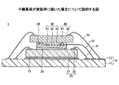
図1は、第1の実施の形態に係る半導体装置を例示する図であり、図1(a)は断面図、図1(b)は中継基板のみを例示する平面図である。図1を参照するに、半導体装置1は、支持体10と、接着層15と、半導体チップ20と、接着層25と、中継基板30と、接着層35と、半導体チップ40と、ボンディングワイヤ51〜53とを有する。
<First Embodiment>
[Structure of Semiconductor Device According to First Embodiment]
1A and 1B are diagrams illustrating a semiconductor device according to the first embodiment. FIG. 1A is a cross-sectional view, and FIG. 1B is a plan view illustrating only a relay substrate. Referring to FIG. 1, a
なお、本実施の形態では、便宜上、半導体チップ40側を上側又は一方の側、支持体10側を下側又は他方の側とする。又、各部位の半導体チップ40側の面を上面又は一方の面、支持体10側の面を下面又は他方の面とする。但し、半導体装置1は天地逆の状態で用いることができ、又は任意の角度で配置することができる。又、平面視とは対象物を支持体10の一方の面の法線方向から視ることを指し、平面形状とは対象物を支持体10の一方の面の法線方向から視た形状を指すものとする。
In the present embodiment, for convenience, the
支持体10は、基体11と、基体11の一方の面に形成された配線12とを有する。基体11としては、例えば、ガラスクロスにエポキシ系樹脂等の絶縁性樹脂を含浸させた所謂ガラスエポキシ基板を用いることができる。基体11として、例えば、ポリイミド樹脂を用いたフレキシブル基板や銅(Cu)等からなるリードフレーム等を用いてもよい。又、基体11は、ビルドアップ基板等の多層配線基板であってもよい。基体11の厚さは、例えば、0.4〜2mm程度とすることができる。
The
配線12の材料としては、例えば、銅(Cu)等を用いることができる。配線12の厚さは、例えば、10〜50μm程度とすることができる。なお、配線12は、ボンディング用パッドやチップ実装用パッド等を含むものである。配線12において、ボンディングワイヤ51、52、及び53が接続される各ボンディング用パッドは互いに絶縁されており、ボンディングワイヤ51、52、及び53を介して対象部位に異なる電圧(接地電位や電源電位、各種信号を含む)を印加可能である。基体11の一方の面に、配線12を選択的に露出する開口部を備えたソルダーレジスト層を設けてもよい。
As a material of the
半導体チップ20は、支持体10上にフェイスアップ状態で積層されている。より詳しくは、半導体チップ20は、配線12のチップ実装用パッド上に接着層15を介して接着されている。半導体チップ20は、半導体集積回路が形成された半導体基板21と、半導体基板21の一方の面に形成されたパッド22とを有する。半導体基板21としては、例えば、シリコン基板等を用いることができる。なお、半導体チップ20は、本発明に係る第1半導体チップの代表的な一例である。
The
パッド22の材料としては、例えば、アルミニウム(Al)、金(Au)、銀(Ag)、パラジウム(Pd)等を用いることができる。パッド22の厚さは、例えば、0.5〜10μm程度とすることができる。パッド22は、ボンディングワイヤ51を介して、配線12のボンディング用パッドに接続されている。ボンディングワイヤ51は、例えば、金(Au)、銅(Cu)、アルミニウム(Al)等からなる金属線である。
As a material of the
接着層15は、例えば、エポキシ系の接着剤を硬化させたものである。接着層15は導電性であっても非導電性であってもよいが、半導体チップ20の裏面(非回路形成面)に配線12を介して所定の電圧(接地電位や電源電位)を印加する必要がある場合には、導電性であることを要する。
For example, the
中継基板30は、半導体チップ20上に積層されている。より詳しくは、中継基板30は、半導体チップ20の回路形成面上に接着層25を介して接着されている。中継基板30は、基体31と、基体31の一方の面に形成された導電部32と、導電部32と電気的に接続された突起電極33とを備えている。基体31としては、例えば、シリコン基板等を用いることができる。基体31として、樹脂基板やガラス基板等を用いてもよい。基体31の厚さは、例えば、100〜500μm程度とすることができる。なお、基体31の厚さが100μm未満になると、ボンディングワイヤ52を打つことが困難となる。
The
導電部32は、基体31の一方の面に積層された金属膜(導体層)である。金属膜の材料としては、例えば、金(Au)やアルミニウム(Al)等を用いることができる。導電部32の厚さは、例えば、0.5〜10μm程度とすることができる。導電部32は、基体31の一方の面の全面に形成してもよいし、突起電極33とボンディングワイヤ52とが電気的に接続されるように基体31の一方の面に選択的に形成(パターニング)してもよい。導電部32は、導電部32の外縁部にボンディングされたボンディングワイヤ52を介して、配線12のボンディング用パッドに接続されている。ボンディングワイヤ52は、例えば、金(Au)、銅(Cu)、アルミニウム(Al)等からなる金属線である。
The
ボンディングワイヤ52は、導電部32の外縁部から略水平方向に伸び、その後支持体10の方向に湾曲している。これにより、ボンディングワイヤ52と半導体チップ40の裏面とが接触するおそれを低減できるため、半導体チップ40の平面形状を中継基板30の平面形状よりも大きくすることが可能となる。但し、半導体チップ40の平面形状を中継基板30の平面形状よりも小さくしてもよい。なお、ボンディングワイヤ52を図1の形状にする方法については後述する。
The
突起電極33は、導電部32の一方の面に半導体チップ40側に突起するように形成されている。突起電極33の個数(最低1個でよい)や配置は任意としてよいが、図1(b)のように導電部32の一方の面の四隅に配置すると好適である。突起電極33としては、例えば、金バンプやはんだバンプ、銅ポスト等を用いることができる。突起電極33の高さは、例えば、20〜70μm程度とすることができる。又、突起電極33の形状は任意としてよいが、図1(a)のように、突起電極33として径が太い部分と径が細い部分とを有するバンプを用いると好適である。
The protruding
なお、突起電極33を導電部32の一方の面の四隅に配することにより、以下の効果を奏する。すなわち、図2に示すように、中継基板30が実装時に傾いてしまった場合に、突起電極33のつぶれ具合により中継基板30の傾きを吸収できると共に、つぶれた突起電極33が半導体チップ40を平行に保つ支えとなり得る。つまり、突起電極33は、半導体チップ40へ電圧印加する機能を有すると共に、半導体チップ40の平行を保つ機能を有し、ボンディングワイヤ53のワイヤボンディング性の向上や全体の高さの均一化にも寄与できる。
In addition, the following effects are produced by arranging the protruding
より詳しく説明すると、突起電極33として径が太い部分と径が細い部分とを有するバンプを用いることにより、中継基板30が半導体チップ20への実装時に傾いた場合に、中継基板30の傾きを吸収できる。すなわち、中継基板30上に半導体チップ40を接続する際に、中継基板30と半導体チップ40との距離が近い部分では、突起電極33の径が細い部分が潰れて距離を短くすることができる。
More specifically, by using bumps having a large diameter portion and a small diameter portion as the protruding
又、突起電極33の径が太い部分は変形し難いため、径が太い部分の高さ以上には潰れ難く、ワイヤボンディング接続に必要な高さを確保できる。一方、中継基板30と半導体チップ40との距離が遠い部分では、突起電極33の径が細い部分を残したまま半導体チップ40と接続することになる。よって、中継基板30が実装時に傾いた場合でも、半導体チップ20と半導体チップ40との平行を保ったまま信頼性高く接続できる。
Moreover, since the part with the large diameter of the
接着層25は、例えば、エポキシ系の接着剤を硬化させたものである。接着層25は、半導体基板21と導電部32とが基体31を介して導通することを避けるため、非導電性の接着層とされている。
For example, the
半導体チップ40は、中継基板30上に接着層35を介してフェイスアップ状態で接着されている。半導体チップ40は、半導体集積回路が形成された半導体基板41と、半導体基板41の一方の面に形成されたパッド42とを有する。半導体基板41としては、例えば、シリコン基板等を用いることができる。なお、半導体チップ40は、本発明に係る第2半導体チップの代表的な一例である。
The
パッド42の材料としては、例えば、金(Au)等を用いることができる。パッド42の厚さは、例えば、0.5〜10μm程度とすることができる。パッド42は、ボンディングワイヤ53を介して、配線12のボンディング用パッドに接続されている。ボンディングワイヤ53は、例えば、金(Au)、銅(Cu)、アルミニウム(Al)等からなる金属線である。
As a material of the
突起電極33は接着層35を貫通しており、突起電極33の上端面が半導体チップ40の裏面(非回路形成面)と接して両者は電気的に接続されている。つまり、半導体チップ40の裏面には、ボンディングワイヤ52、導電部32、及び突起電極33を介して、支持体10の配線12から所定の電圧(接地電位や電源電位)を印加可能である。半導体チップ40の裏面を所定の電位に固定することにより、半導体チップ40の電気的特性を向上できる。なお、裏面を所定の電位に固定する対象となる半導体チップは、所謂アナログチップ(主としてアナログ回路を形成したチップ)である。
The protruding
接着層35は、例えば、エポキシ系の接着剤を硬化させたものである。接着層35は非導電性の接着層である。接着層35として導電性の接着層を用いても電気的な動作に支障はないが、導電性の接着剤は非導電性の接着剤よりも密着力が低いため、本実施の形態では、接着層35を非導電性の接着剤を硬化させた非導電性の接着層としている。なお、接着層35は、本発明に係る非導電性接着層の代表的な一例である。
For example, the
[第1の実施の形態に係る半導体装置の製造方法]
図3及び図4は、第1の実施の形態に係る半導体装置の製造工程を例示する図である。まず、図3に示す工程では中継基板30を作製する。具体的には、図3(a)に示すように、最終的に個片化されて基体31となるシリコンウェハ310を準備する。但し、シリコンウェハに代えて、樹脂基板やガラス基板等を準備してもよい。シリコンウェハ310は薄型化されてなく、その厚さは、例えば600〜800μm程度とすることができる。なお、Cはシリコンウェハ310等を切断する位置(以降、切断位置Cとする)を示している。シリコンウェハ310は、切断位置Cにより、図1(b)に示すような中継基板30となる矩形状の複数の領域に区分されている。
[Method of Manufacturing Semiconductor Device According to First Embodiment]
3 and 4 are diagrams illustrating the manufacturing process of the semiconductor device according to the first embodiment. First, in the step shown in FIG. 3, the
次に、シリコンウェハ310の一方の面に、最終的に個片化されて導電部32となる金属膜320をスパッタ法等により形成する。金属膜320の材料としては、例えば、金(Au)やアルミニウム(Al)等を用いることができる。金属膜320の厚さは、例えば、0.5〜10μm程度とすることができる。金属膜320は、シリコンウェハ310の一方の面の全面に形成してもよいし、後工程で突起電極33とボンディングワイヤ52とが電気的に接続されるようにシリコンウェハ310の一方の面に選択的に形成(パターニング)してもよい。
Next, on one surface of the
次に、図3(b)に示すように、バックサイドグラインダ等を用いて、シリコンウェハ310を他方の面側から研削して薄型化する。薄型化後のシリコンウェハ310の厚さは、例えば、100〜500μm程度とすることができる。
Next, as shown in FIG. 3B, the
次に、図3(c)に示すように、例えば、金属膜320の一方の面の切断位置Cにより区分された各領域の四隅に、突起電極33を形成する。突起電極33としては、例えば、金バンプやはんだバンプ、銅ポスト等を用いることができるが、突起電極33として金バンプを用いる場合には、ワイヤボンダを使用して金属膜320の一方の面に形成できる。なお、突起電極33は後述の図4(c)に示す工程で押圧されるため、この時点では最終的な高さ(図4(c)に示す工程後の高さ)よりも高く形成しておくことが好ましい。
Next, as illustrated in FIG. 3C, for example, the protruding
次に、図3(d)に示すように、突起電極33及び金属膜320が形成されたシリコンウェハ310を、例えば、ダイシング等により切断位置Cで切断して個片化する。これにより、シリコンウェハ310及び金属膜320から基体31及び導電部32が形成され、複数の中継基板30が完成する。
Next, as shown in FIG. 3D, the
次に、図4(a)に示す工程では、基体11及び配線12を有する支持体10を準備する。基体11としては、例えば、ガラスクロスにエポキシ系樹脂等の絶縁性樹脂を含浸させた所謂ガラスエポキシ基板を用いることができる。基体11として、例えば、ポリイミド樹脂を用いたフレキシブル基板や銅(Cu)等からなるリードフレーム等を用いてもよい。又、基体11は、ビルドアップ基板等の多層配線基板であってもよい。基体11の厚さは、例えば、0.4〜2mm程度とすることができる。
Next, in the step shown in FIG. 4A, the
次に、支持体10の配線12のチップ実装用パッド上に、接着層15を介して、半導体基板21及びパッド22を有する半導体チップ20をフェイスアップ状態で積層する。接着層15は、例えば、エポキシ系の接着剤を硬化させたものである。接着層15は導電性であっても非導電性であってもよいが、半導体チップ20の裏面(非回路形成面)に配線12を介して所定の電圧(接地電位や電源電位)を印加する必要がある場合には、導電性であることを要する。
Next, the
次に、例えば、ワイヤボンダを用いて、半導体チップ20のパッド22と配線12のボンディング用パッドとをボンディングワイヤ51を介して接続する。ボンディングワイヤ51としては、例えば、金(Au)、銅(Cu)、アルミニウム(Al)等からなる金属線を用いることができる。
Next, the
次に、図4(b)に示す工程では、図3に示す工程で作製した中継基板30を、半導体チップ20の回路形成面上に接着層25を介して接着する。接着層25は、例えば、エポキシ系の接着剤を硬化させたものである。接着層25は、半導体基板21と導電部32とが基体31を介して導通することを避けるため、非導電性の接着層とされている。
Next, in the step shown in FIG. 4B, the
次に、例えば、ワイヤボンダを用いて、導電部32と配線12のボンディング用パッドとをボンディングワイヤ52を介して接続する。ボンディングワイヤ52としては、例えば、金(Au)、銅(Cu)、アルミニウム(Al)等からなる金属線を用いることができる。
Next, the
なお、ボンディングワイヤ52は、導電部32の外縁部から略水平方向に伸び、その後支持体10の方向に湾曲している。これにより、ボンディングワイヤ52と半導体チップ40の裏面とが接触するおそれを低減できるため、半導体チップ40の平面形状を中継基板30の平面形状よりも大きくすることが可能となる。ボンディングワイヤ52を図4(b)の形状にするには、配線12側からワイヤボンディングを行えばよい。
The
すなわち、ボンディングワイヤの先端部に形成されたボンディングボールを配線12の上面に接触させ、キャピラリにより所定の荷重をかけながら超音波を印加する。これにより、配線12の上面にボンディングワイヤ52の一端が形成される。次に、導電部32の上面と略同一高さとなるまでキャピラリを上昇させ、キャピラリを導電部32の外縁部近傍に水平移動させる。そして、導電部32の外縁部にボンディングワイヤ52の他端となる部分を接合し、不要部を切断する。なお、このような方法をリバースボンディングと称する場合がある。半導体チップ40の平面形状が中継基板30の平面形状よりも小さい場合には、リバースボンディングを行わなくてもよい。
That is, a bonding ball formed at the tip of the bonding wire is brought into contact with the upper surface of the
次に、中継基板30上に、突起電極33を覆うように、硬化すると接着層35となるエポキシ系の熱硬化性接着剤等を塗布する。なお、この工程では、接着剤は未硬化である。
Next, an epoxy-based thermosetting adhesive or the like that becomes the
次に、図4(c)に示す工程では中継基板30上に、例えば、エポキシ系の熱硬化性接着剤等を介して、半導体基板41及びパッド42を有する半導体チップ40をフェイスアップ状態で積層する。そして、エポキシ系の熱硬化性接着剤等を加熱しながら、半導体チップ40を中継基板30側に押圧し、エポキシ系の熱硬化性接着剤等を硬化させて接着層35を形成する。半導体チップ40を中継基板30側に押圧することにより突起電極33の先端部がつぶれ、突起電極33の上端面が半導体チップ40の裏面(非回路形成面)と接して両者は電気的に接続される。
Next, in the step shown in FIG. 4C, the
なお、接着層35は非導電性の接着層である。接着層35として導電性の接着層を用いても電気的な動作に支障はないが、導電性の接着剤は非導電性の接着剤よりも密着力が低いため、本実施の形態では、接着層35を非導電性の接着剤を硬化させた非導電性の接着層としている。
The
図4(c)に示す工程の後、例えば、ワイヤボンダを用いて、半導体チップ40のパッド42と配線12のボンディング用パッドとをボンディングワイヤ53を介して接続することにより、半導体装置1(図1参照)が完成する。ボンディングワイヤ53としては、例えば、金(Au)、銅(Cu)、アルミニウム(Al)等からなる金属線を用いることができる。
After the step shown in FIG. 4C, the semiconductor device 1 (FIG. 1) is formed by connecting the
このように、第1の実施の形態に係る半導体装置1では、接着層35として、導電性の接着剤を用いることなく非導電性の接着剤を用いることが可能となるため、電気的な損失を低減できると共に、接着する対象物に対して十分な密着力を確保できる。
As described above, in the
すなわち、第1の実施の形態に係る半導体装置1では、半導体チップ40の裏面への電圧の印加に導電部32に接続された突起電極33を用いている。そのため、従来の半導体装置のように電気伝導率の低い導電性の接着層を用いる必要がなく、効果的に半導体チップ40の裏面へ電圧を印加可能となり、電気的な損失を低減できる。
That is, in the
又、第1の実施の形態に係る半導体装置1において、導電部32を基体31の面全体に形成した場合には、ワイヤボンディング接続の際、導電部32の任意の位置にボンディングワイヤを打つことが可能となり、ワイヤボンディング接続の自由度を向上できる。なお、従来の半導体装置では、予め所定位置に形成したパッド上にしかボンディングワイヤを打つことができない。
Further, in the
又、突起電極33として径が太い部分と径が細い部分とを有するバンプを用いることにより、中継基板30が半導体チップ20への実装時に傾いた場合に、中継基板30の傾きを吸収できる。すなわち、中継基板30上に半導体チップ40を接続する際に、中継基板30と半導体チップ40との距離が近い部分では、突起電極33の径が細い部分が潰れて距離を短くすることができる。又、突起電極33の径が太い部分は変形し難いため、径が太い部分の高さ以上には潰れ難く、ワイヤボンディング接続に必要な高さを確保できる。一方、中継基板30と半導体チップ40との距離が遠い部分では、突起電極33の径が細い部分を残したまま半導体チップ40と接続することになる。よって、中継基板30が実装時に傾いた場合でも、半導体チップ20と半導体チップ40との平行を保ったまま信頼性高く接続できる。
Further, by using bumps having a large diameter portion and a thin diameter portion as the protruding
又、従来の半導体装置では、接着層を介して半導体チップの裏面に所定の電圧を印加していたため、高価な導電性の接着層を用いることが必須要件であった。これに対して、本実施の形態では、半導体チップ40の裏面が突起電極33の上端面と接しており、突起電極33を介して半導体チップ40の裏面に所定の電圧を印加可能であるため、接着層35を導電性とする必要はない。その結果、接着層35として、高価な導電性の接着剤を用いることなく安価な非導電性の接着剤を用いることが可能となり、半導体装置1の低コスト化に寄与できる。
Further, in the conventional semiconductor device, since a predetermined voltage is applied to the back surface of the semiconductor chip via the adhesive layer, it is essential to use an expensive conductive adhesive layer. On the other hand, in the present embodiment, the back surface of the
〈第1の実施の形態の変形例〉
第1の実施の形態の変形例では、第1の実施の形態とは異なる中継基板を用いる例を示す。なお、第1の実施の形態の変形例において、既に説明した実施の形態と同一構成部品についての説明は省略する。
<Modification of First Embodiment>
In the modification of the first embodiment, an example in which a relay board different from that of the first embodiment is used is shown. In the modification of the first embodiment, the description of the same components as those of the already described embodiment is omitted.
図5は、第1の実施の形態の変形例に係る半導体装置を例示する断面図である。図5を参照するに、第1の実施の形態の変形例に係る半導体装置1Aは、中継基板30が中継基板30Aに置換された点が第1の実施の形態に係る半導体装置1(図1参照)と相違する。
FIG. 5 is a cross-sectional view illustrating a semiconductor device according to a variation of the first embodiment. Referring to FIG. 5, the
中継基板30Aは、半導体チップ20の回路形成面上に接着層25を介して接着されている。中継基板30Aは、金属板31Aと、金属板31Aと電気的に接続された突起電極33とを備えている。金属板31Aとしては、例えば、アルミ板や銅板等を用いることができる。金属板31Aの厚さは、例えば、100〜500μm程度とすることができる。金属板31Aの表面にめっき処理等を施しても構わない。なお、金属板31Aは、本発明に係る導電部の代表的な一例である。
The
中継基板は、半導体チップ40の裏面に印加する電圧を中継する機能を実現できればよい。そのため、中継基板30(図1参照)のように絶縁体や半導体である基体31上に導電部32を形成して導電部32に突起電極33を設ける構成でもよいし、中継基板30Aのように金属板31A(導電部)に直接突起電極33を設ける構成でもよい。この場合も、第1の実施の形態と同様の効果を奏する。
The relay substrate only needs to realize a function of relaying a voltage applied to the back surface of the
〈第2の実施の形態〉
第2の実施の形態では、半導体チップ40の裏面に印加するのと同一の電圧を半導体チップ20の裏面にも印加する例を示す。なお、第2の実施の形態において、既に説明した実施の形態と同一構成部品についての説明は省略する。
<Second Embodiment>
In the second embodiment, an example in which the same voltage applied to the back surface of the
図6は、第2の実施の形態に係る半導体装置を例示する断面図である。図6を参照するに、第2の実施の形態に係る半導体装置1Bは、半導体チップ20が支持体10上にフリップチップ実装された点が第1の実施の形態に係る半導体装置1(図1参照)と相違する。又、半導体装置1Bは、接着層25及び中継基板30が接着層25B及び中継基板30Bに置換された点が第1の実施の形態に係る半導体装置1(図1参照)と相違する。
FIG. 6 is a cross-sectional view illustrating a semiconductor device according to the second embodiment. Referring to FIG. 6, in the
半導体チップ20は、支持体10上にフェイスダウン状態で積層されており、半導体チップ20のパッド22は、配線12のチップ実装用パッドとバンプ60を介して電気的に接続されている。バンプ60としては、例えば、はんだバンプ等を用いることができる。半導体チップ20と支持体10の互いに対向する面の間には、バンプ60を被覆するアンダーフィル樹脂70が充填されている。
The
中継基板30Bは、基体31と、導電部32と、突起電極33と、基体31の他方の面に形成された導電部32Bと、導電部32Bと電気的に接続された突起電極33Bと、貫通電極34とを有する。導電部32と導電部32Bとは、貫通電極34を介して電気的に接続されている。その結果、突起電極33と突起電極33Bとは電気的に接続されている。導電部32B及び突起電極33Bの材料や形状等は、例えば、導電部32及び突起電極33と同様とすることができる。貫通電極34の材料としては、例えば、銅(Cu)等を用いることができる。
The
中継基板30Bは、導電部32B及び突起電極33Bを半導体チップ20の裏面側に向けて、接着層25Bを介して、半導体チップ20上に積層されている。接着層25Bは、例えば、エポキシ系の接着剤を硬化させたものである。接着層25Bは非導電性の接着層である。接着層25Bとして導電性の接着層を用いても電気的な動作に支障はないが、導電性の接着剤は非導電性の接着剤よりも密着力が低いため、本実施の形態では、接着層25Bを非導電性の接着剤を硬化させた非導電性の接着層としている。なお、接着層25Bは、本発明に係る第2非導電性接着層の代表的な一例である。
The
突起電極33Bは接着層25Bを貫通しており、突起電極33Bの下端面が半導体チップ20の裏面(非回路形成面)と接して両者は電気的に接続されている。つまり、半導体チップ20の裏面には、ボンディングワイヤ52、導電部32、貫通電極34、導電部32B、及び突起電極33Bを介して、支持体10の配線12から所定の電圧を印加可能である。すなわち、半導体チップ40の裏面に印加するのと同一の電圧を半導体チップ20の裏面にも印加できる。なお、突起電極33Bは、本発明に係る第2突起電極の代表的な一例である。
The protruding
本実施の形態では、半導体チップ40の裏面が突起電極33の上端面と接しており、突起電極33を介して半導体チップ40の裏面に所定の電圧を印加可能である。又、半導体チップ20の裏面が突起電極33Bの下端面と接しており、突起電極33Bを介して半導体チップ20の裏面に所定の電圧を印加可能である。そのため、接着層35及び25Bを導電性とする必要はない。
In the present embodiment, the back surface of the
このように、本実施の形態では、接着層35及び25Bとして、導電性の接着剤を用いることなく非導電性の接着剤を用いることが可能となるため、第1の実施の形態と同様の効果を奏する。
As described above, in the present embodiment, a non-conductive adhesive can be used as the
なお、導電部32、貫通電極34、及び導電部32Bに代えて1枚の金属板を用い、金属板の上面に突起電極33を設け、金属板の下面に突起電極33Bを設けてもよい。
Note that a single metal plate may be used in place of the
〈第3の実施の形態〉
第3の実施の形態では、半導体チップ40の裏面に印加するのと異なる電圧を半導体チップ20の裏面に印加する例を示す。なお、第3の実施の形態において、既に説明した実施の形態と同一構成部品についての説明は省略する。
<Third Embodiment>
In the third embodiment, an example in which a voltage different from that applied to the back surface of the
図7は、第3の実施の形態に係る半導体装置を例示する断面図である。図7を参照するに、第3の実施の形態に係る半導体装置1Cは、中継基板30A及び30Cの2つの中継基板を用いる点が第2の実施の形態に係る半導体装置1B(図6参照)と相違する。
FIG. 7 is a cross-sectional view illustrating a semiconductor device according to the third embodiment. Referring to FIG. 7, the semiconductor device 1C according to the third embodiment uses the two
中継基板30Cは、半導体チップ20と中継基板30Aとの間に配置され、接着層25Bを介して半導体チップ20上に積層されている。中継基板30Cは、金属板31Cと、金属板31Cと電気的に接続された突起電極33Cとを備えている。金属板31Cと突起電極33Cの材料や形状等は、例えば、金属板31Aと突起電極33と同様とすることができる。つまり、中継基板30Cとして、中継基板30Aと同様のものを用いてもよい。なお、中継基板30Cは、本発明に係る第2中継基板の代表的な一例である。又、金属板31Cは本発明に係る第2導電部の、突起電極33Cは本発明に係る第2突起電極の代表的な一例である。
The relay substrate 30C is disposed between the
中継基板30Cは、突起電極33Cを半導体チップ20の裏面側に向けて、接着層25Bを介して、半導体チップ20上に積層されている。中継基板30Aは、突起電極33を半導体チップ40の裏面側に向けて、接着層45を介して、中継基板30C上に積層されている。金属板31Cの接着層45側の面は、ボンディングワイヤ54を介して、配線12のボンディング用パッドに接続されている。ボンディングワイヤ54は、例えば、金(Au)、銅(Cu)、アルミニウム(Al)等からなる金属線である。
The relay substrate 30C is laminated on the
半導体チップ40の裏面と半導体チップ20の裏面に異なる電圧を印加するためには、突起電極33と突起電極33Cとが導通しないようにする必要がある。つまり、金属板31Aと金属板31Cとを絶縁する必要がある。そのため、接着層45としては、非導電性の接着剤を硬化させた非導電性の接着層を用いている。
In order to apply different voltages to the back surface of the
半導体チップ40の裏面は、中継基板30Aの突起電極33の上端面と接しており、両者は導通している。つまり、半導体チップ40の裏面には、ボンディングワイヤ52、金属板31A、及び突起電極33を介して、支持体10の配線12から所定の電圧を印加可能である。又、半導体チップ20の裏面は、中継基板30Cの突起電極33Cの下端面と接しており、両者は導通している。つまり、半導体チップ20の裏面には、ボンディングワイヤ54、金属板31C、及び突起電極33Cを介して、支持体10の配線12から所定の電圧を印加可能である。
The back surface of the
ボンディングワイヤ52及び54が接続される各ボンディング用パッドは互いに絶縁されており、ボンディングワイヤ52及び54を介して対象部位に異なる電圧(接地電位や電源電位)を印加可能である。すなわち、半導体チップ40の裏面に印加するのと異なる電圧を半導体チップ20の裏面に印加できる。
The bonding pads to which the
本実施の形態では、半導体チップ40の裏面が突起電極33の上端面と接しており、突起電極33を介して半導体チップ40の裏面に所定の電圧を印加可能である。又、半導体チップ20の裏面が突起電極33Cの下端面と接しており、突起電極33Cを介して半導体チップ20の裏面に所定の電圧を印加可能である。そのため、第2の実施の形態と同様に、接着層35及び25Bを導電性とする必要はない。
In the present embodiment, the back surface of the
このように、本実施の形態では、接着層35及び25Bとして、導電性の接着剤を用いることなく非導電性の接着剤を用いることが可能となるため、第1の実施の形態と同様の効果を奏する。
As described above, in the present embodiment, a non-conductive adhesive can be used as the
以上、好ましい実施の形態及びその変形例について詳説したが、上述した実施の形態及びその変形例に制限されることはなく、特許請求の範囲に記載された範囲を逸脱することなく、上述した実施の形態及びその変形例に種々の変形及び置換を加えることができる。 The preferred embodiment and its modification have been described in detail above, but the present invention is not limited to the above-described embodiment and its modification, and the above-described implementation is performed without departing from the scope described in the claims. Various modifications and substitutions can be added to the embodiment and its modifications.
1、1A、1B、1C 半導体装置
10 支持体
11、31 基体
12 配線
15、25、25B、35、45 接着層
20、40 半導体チップ
21、41 半導体基板
22、42 パッド
30、30A、30B、30C 中継基板
31A、31C 金属板
32、32B 導電部
33、33B、33C 突起電極
34 貫通電極
51、52、53、54 ボンディングワイヤ
60 バンプ
70 アンダーフィル樹脂
310 シリコンウェハ
320 金属膜
1, 1A, 1B,
Claims (3)
前記支持体上にフェイスダウン状態で積層された第1半導体チップと、
前記第1半導体チップ上に第1非導電性接着層を介して積層された中継基板と、
前記中継基板上に第2非導電性接着層を介してフェイスアップ状態で積層された第2半導体チップと、を有し、
前記中継基板は、樹脂で形成された基体と、前記基体の前記第1半導体チップ側に形成された導体層である第1導電部と、前記第1導電部と電気的に接続された第1突起電極と、前記基体の前記第2半導体チップ側に形成された導体層である第2導電部と、前記第2導電部と電気的に接続された第2突起電極と、を備え、
前記第1導電部と前記第2導電部とは、前記基体に形成された貫通電極を介して電気的に接続され、
前記第2導電部は、前記中継基板の前記第2半導体チップと対向する面側に接続された金属線を介して前記支持体上の配線と電気的に接続され、
前記第1突起電極は、前記第1非導電性接着層を貫通して前記第1半導体チップの非回路形成面と接して導通し、
前記第2突起電極は、前記第2非導電性接着層を貫通して前記第2半導体チップの非回路形成面と接して導通している半導体装置。 A support with wiring,
A first semiconductor chip stacked face down on the support;
A relay substrate laminated on the first semiconductor chip via a first non-conductive adhesive layer;
A second semiconductor chip laminated in a face-up state on the relay substrate via a second non-conductive adhesive layer,
The relay substrate includes a base made of resin, a first conductive portion that is a conductor layer formed on the first semiconductor chip side of the base, and a first electrically connected to the first conductive portion. A projecting electrode, a second conductive part which is a conductor layer formed on the second semiconductor chip side of the base, and a second projecting electrode electrically connected to the second conductive part ,
The first conductive part and the second conductive part are electrically connected via a through electrode formed in the base body,
The second conductive part is electrically connected to the wiring on the support through a metal wire connected to the surface of the relay substrate facing the second semiconductor chip,
The first protruding electrode penetrates the first non-conductive adhesive layer and is in contact with the non-circuit forming surface of the first semiconductor chip;
The second protruding electrode is a semiconductor device that is electrically connected to the non-circuit forming surface of the second semiconductor chip through the second non-conductive adhesive layer.
前記第1突起電極において、前記径が太い部分側が前記中継基板と接続され、前記径が細い部分側が前記第1半導体チップと接続され、
前記第2突起電極において、前記径が太い部分側が前記中継基板と接続され、前記径が細い部分側が前記第2半導体チップと接続されている請求項1記載の半導体装置。 The first protruding electrode and the second protruding electrode are bumps having a portion having a large diameter and a portion having a small diameter,
In the first protruding electrode, the portion having the large diameter is connected to the relay substrate, and the portion having the small diameter is connected to the first semiconductor chip ,
Wherein the second protruding electrode, the diameter of the thick portion side is connected to the relay substrate, a semiconductor device according to claim 1, wherein the diameter of the narrowest part side is connected to the second semiconductor chip.
Priority Applications (2)
| Application Number | Priority Date | Filing Date | Title |
|---|---|---|---|
| JP2013232448A JP6242665B2 (en) | 2013-11-08 | 2013-11-08 | Semiconductor device |
| US14/517,993 US9508670B2 (en) | 2013-11-08 | 2014-10-20 | Semiconductor device including semiconductor chips stacked via relay substrate |
Applications Claiming Priority (1)
| Application Number | Priority Date | Filing Date | Title |
|---|---|---|---|
| JP2013232448A JP6242665B2 (en) | 2013-11-08 | 2013-11-08 | Semiconductor device |
Publications (3)
| Publication Number | Publication Date |
|---|---|
| JP2015095489A JP2015095489A (en) | 2015-05-18 |
| JP2015095489A5 JP2015095489A5 (en) | 2016-09-23 |
| JP6242665B2 true JP6242665B2 (en) | 2017-12-06 |
Family
ID=53043083
Family Applications (1)
| Application Number | Title | Priority Date | Filing Date |
|---|---|---|---|
| JP2013232448A Active JP6242665B2 (en) | 2013-11-08 | 2013-11-08 | Semiconductor device |
Country Status (2)
| Country | Link |
|---|---|
| US (1) | US9508670B2 (en) |
| JP (1) | JP6242665B2 (en) |
Families Citing this family (4)
| Publication number | Priority date | Publication date | Assignee | Title |
|---|---|---|---|---|
| US10229887B2 (en) | 2016-03-31 | 2019-03-12 | Intel Corporation | Systems and methods for electromagnetic interference shielding |
| WO2018148444A1 (en) * | 2017-02-10 | 2018-08-16 | Behrooz Mehr | Grounding techniques for backside-biased semiconductor dice and related devices, systems and methods |
| JP2018137342A (en) * | 2017-02-22 | 2018-08-30 | 株式会社村田製作所 | Semiconductor device and manufacturing method of the same |
| JP7230419B2 (en) * | 2018-10-16 | 2023-03-01 | 富士電機株式会社 | Semiconductor device, method for manufacturing semiconductor device |
Family Cites Families (9)
| Publication number | Priority date | Publication date | Assignee | Title |
|---|---|---|---|---|
| JPH06120464A (en) * | 1992-10-06 | 1994-04-28 | Matsushita Electric Ind Co Ltd | Semiconductor device |
| JP2000269411A (en) * | 1999-03-17 | 2000-09-29 | Shinko Electric Ind Co Ltd | Semiconductor device and manufacture thereof |
| US6555917B1 (en) * | 2001-10-09 | 2003-04-29 | Amkor Technology, Inc. | Semiconductor package having stacked semiconductor chips and method of making the same |
| JP2004031649A (en) * | 2002-06-26 | 2004-01-29 | Sony Corp | Semiconductor device and its manufacturing method |
| JP3596813B2 (en) * | 2002-08-09 | 2004-12-02 | 沖電気工業株式会社 | Semiconductor device |
| JP2005277356A (en) * | 2004-03-26 | 2005-10-06 | Sanyo Electric Co Ltd | Circuit device |
| JP2008034567A (en) * | 2006-07-27 | 2008-02-14 | Fujitsu Ltd | Semiconductor device and manufacturing method therefor |
| US7768135B1 (en) * | 2008-04-17 | 2010-08-03 | Amkor Technology, Inc. | Semiconductor package with fast power-up cycle and method of making same |
| JP2013110188A (en) * | 2011-11-18 | 2013-06-06 | Semiconductor Components Industries Llc | Semiconductor device and manufacturing method of the same |
-
2013
- 2013-11-08 JP JP2013232448A patent/JP6242665B2/en active Active
-
2014
- 2014-10-20 US US14/517,993 patent/US9508670B2/en active Active
Also Published As
| Publication number | Publication date |
|---|---|
| US9508670B2 (en) | 2016-11-29 |
| JP2015095489A (en) | 2015-05-18 |
| US20150130053A1 (en) | 2015-05-14 |
Similar Documents
| Publication | Publication Date | Title |
|---|---|---|
| JP3565319B2 (en) | Semiconductor device and manufacturing method thereof | |
| JP4474431B2 (en) | Semiconductor package and manufacturing method thereof | |
| JP3994262B2 (en) | Semiconductor device and manufacturing method thereof, circuit board, and electronic apparatus | |
| JP3633559B2 (en) | Semiconductor device and manufacturing method thereof, circuit board, and electronic apparatus | |
| JP3822040B2 (en) | Electronic device and manufacturing method thereof | |
| JP5529371B2 (en) | Semiconductor device and manufacturing method thereof | |
| US20060192294A1 (en) | Chip scale package having flip chip interconnect on die paddle | |
| JP2001015679A (en) | Semiconductor device and manufacture thereof | |
| CN110473796A (en) | Multiple underfills for flip chip encapsulating piece | |
| US20120273946A1 (en) | Semiconductor device | |
| JP6242665B2 (en) | Semiconductor device | |
| JP4379693B2 (en) | Semiconductor device and manufacturing method thereof | |
| JP2011243724A (en) | Semiconductor device and method for manufacturing the same | |
| JP2000277649A (en) | Semiconductor and manufacture of the same | |
| JP2000299432A (en) | Manufacture of semiconductor device | |
| US9355988B2 (en) | Semiconductor device | |
| JP2002343930A (en) | Semiconductor device | |
| JP3824545B2 (en) | Wiring board, semiconductor device using the same, and manufacturing method thereof | |
| JP2007150346A (en) | Semiconductor device and method of manufacturing same, circuit board, and electronic apparatus | |
| JP2004363319A (en) | Mount substrate and semiconductor device | |
| JP2004031649A (en) | Semiconductor device and its manufacturing method | |
| JP3337922B2 (en) | Semiconductor device and manufacturing method thereof | |
| TWI393197B (en) | Chip package | |
| US8703533B2 (en) | Semiconductor package and method for manufacturing the same | |
| JPWO2018211614A1 (en) | Thin film capacitor structure and semiconductor device provided with the thin film capacitor structure |
Legal Events
| Date | Code | Title | Description |
|---|---|---|---|
| A521 | Request for written amendment filed |
Free format text: JAPANESE INTERMEDIATE CODE: A523 Effective date: 20160805 |
|
| A621 | Written request for application examination |
Free format text: JAPANESE INTERMEDIATE CODE: A621 Effective date: 20160805 |
|
| A977 | Report on retrieval |
Free format text: JAPANESE INTERMEDIATE CODE: A971007 Effective date: 20170420 |
|
| A131 | Notification of reasons for refusal |
Free format text: JAPANESE INTERMEDIATE CODE: A131 Effective date: 20170509 |
|
| A521 | Request for written amendment filed |
Free format text: JAPANESE INTERMEDIATE CODE: A523 Effective date: 20170615 |
|
| TRDD | Decision of grant or rejection written | ||
| A01 | Written decision to grant a patent or to grant a registration (utility model) |
Free format text: JAPANESE INTERMEDIATE CODE: A01 Effective date: 20171024 |
|
| A61 | First payment of annual fees (during grant procedure) |
Free format text: JAPANESE INTERMEDIATE CODE: A61 Effective date: 20171108 |
|
| R150 | Certificate of patent or registration of utility model |
Ref document number: 6242665 Country of ref document: JP Free format text: JAPANESE INTERMEDIATE CODE: R150 |