JP6231069B2 - Submount, assembly including submount, assembly method, and assembly apparatus - Google Patents
Submount, assembly including submount, assembly method, and assembly apparatus Download PDFInfo
- Publication number
- JP6231069B2 JP6231069B2 JP2015500376A JP2015500376A JP6231069B2 JP 6231069 B2 JP6231069 B2 JP 6231069B2 JP 2015500376 A JP2015500376 A JP 2015500376A JP 2015500376 A JP2015500376 A JP 2015500376A JP 6231069 B2 JP6231069 B2 JP 6231069B2
- Authority
- JP
- Japan
- Prior art keywords
- submount
- electronic component
- attachment
- carrier
- assembly
- Prior art date
- Legal status (The legal status is an assumption and is not a legal conclusion. Google has not performed a legal analysis and makes no representation as to the accuracy of the status listed.)
- Expired - Fee Related
Links
Images


Classifications
-
- H—ELECTRICITY
- H05—ELECTRIC TECHNIQUES NOT OTHERWISE PROVIDED FOR
- H05K—PRINTED CIRCUITS; CASINGS OR CONSTRUCTIONAL DETAILS OF ELECTRIC APPARATUS; MANUFACTURE OF ASSEMBLAGES OF ELECTRICAL COMPONENTS
- H05K1/00—Printed circuits
- H05K1/02—Details
- H05K1/0277—Bendability or stretchability details
- H05K1/0283—Stretchable printed circuits
-
- H—ELECTRICITY
- H05—ELECTRIC TECHNIQUES NOT OTHERWISE PROVIDED FOR
- H05K—PRINTED CIRCUITS; CASINGS OR CONSTRUCTIONAL DETAILS OF ELECTRIC APPARATUS; MANUFACTURE OF ASSEMBLAGES OF ELECTRICAL COMPONENTS
- H05K1/00—Printed circuits
- H05K1/02—Details
- H05K1/11—Printed elements for providing electric connections to or between printed circuits
- H05K1/111—Pads for surface mounting, e.g. lay-out
-
- H—ELECTRICITY
- H05—ELECTRIC TECHNIQUES NOT OTHERWISE PROVIDED FOR
- H05K—PRINTED CIRCUITS; CASINGS OR CONSTRUCTIONAL DETAILS OF ELECTRIC APPARATUS; MANUFACTURE OF ASSEMBLAGES OF ELECTRICAL COMPONENTS
- H05K1/00—Printed circuits
- H05K1/02—Details
- H05K1/09—Use of materials for the conductive, e.g. metallic pattern
-
- H—ELECTRICITY
- H05—ELECTRIC TECHNIQUES NOT OTHERWISE PROVIDED FOR
- H05K—PRINTED CIRCUITS; CASINGS OR CONSTRUCTIONAL DETAILS OF ELECTRIC APPARATUS; MANUFACTURE OF ASSEMBLAGES OF ELECTRICAL COMPONENTS
- H05K1/00—Printed circuits
- H05K1/18—Printed circuits structurally associated with non-printed electric components
- H05K1/181—Printed circuits structurally associated with non-printed electric components associated with surface mounted components
-
- H—ELECTRICITY
- H05—ELECTRIC TECHNIQUES NOT OTHERWISE PROVIDED FOR
- H05K—PRINTED CIRCUITS; CASINGS OR CONSTRUCTIONAL DETAILS OF ELECTRIC APPARATUS; MANUFACTURE OF ASSEMBLAGES OF ELECTRICAL COMPONENTS
- H05K13/00—Apparatus or processes specially adapted for manufacturing or adjusting assemblages of electric components
-
- H—ELECTRICITY
- H05—ELECTRIC TECHNIQUES NOT OTHERWISE PROVIDED FOR
- H05K—PRINTED CIRCUITS; CASINGS OR CONSTRUCTIONAL DETAILS OF ELECTRIC APPARATUS; MANUFACTURE OF ASSEMBLAGES OF ELECTRICAL COMPONENTS
- H05K1/00—Printed circuits
- H05K1/02—Details
- H05K1/03—Use of materials for the substrate
- H05K1/038—Textiles
-
- H—ELECTRICITY
- H05—ELECTRIC TECHNIQUES NOT OTHERWISE PROVIDED FOR
- H05K—PRINTED CIRCUITS; CASINGS OR CONSTRUCTIONAL DETAILS OF ELECTRIC APPARATUS; MANUFACTURE OF ASSEMBLAGES OF ELECTRICAL COMPONENTS
- H05K1/00—Printed circuits
- H05K1/18—Printed circuits structurally associated with non-printed electric components
- H05K1/189—Printed circuits structurally associated with non-printed electric components characterised by the use of flexible or folded printed circuits
-
- H—ELECTRICITY
- H05—ELECTRIC TECHNIQUES NOT OTHERWISE PROVIDED FOR
- H05K—PRINTED CIRCUITS; CASINGS OR CONSTRUCTIONAL DETAILS OF ELECTRIC APPARATUS; MANUFACTURE OF ASSEMBLAGES OF ELECTRICAL COMPONENTS
- H05K2201/00—Indexing scheme relating to printed circuits covered by H05K1/00
- H05K2201/09—Shape and layout
- H05K2201/09209—Shape and layout details of conductors
- H05K2201/09218—Conductive traces
- H05K2201/09263—Meander
-
- H—ELECTRICITY
- H05—ELECTRIC TECHNIQUES NOT OTHERWISE PROVIDED FOR
- H05K—PRINTED CIRCUITS; CASINGS OR CONSTRUCTIONAL DETAILS OF ELECTRIC APPARATUS; MANUFACTURE OF ASSEMBLAGES OF ELECTRICAL COMPONENTS
- H05K2201/00—Indexing scheme relating to printed circuits covered by H05K1/00
- H05K2201/09—Shape and layout
- H05K2201/09209—Shape and layout details of conductors
- H05K2201/09372—Pads and lands
- H05K2201/09418—Special orientation of pads, lands or terminals of component, e.g. radial or polygonal orientation
-
- H—ELECTRICITY
- H05—ELECTRIC TECHNIQUES NOT OTHERWISE PROVIDED FOR
- H05K—PRINTED CIRCUITS; CASINGS OR CONSTRUCTIONAL DETAILS OF ELECTRIC APPARATUS; MANUFACTURE OF ASSEMBLAGES OF ELECTRICAL COMPONENTS
- H05K2201/00—Indexing scheme relating to printed circuits covered by H05K1/00
- H05K2201/10—Details of components or other objects attached to or integrated in a printed circuit board
- H05K2201/10007—Types of components
- H05K2201/10106—Light emitting diode [LED]
-
- H—ELECTRICITY
- H05—ELECTRIC TECHNIQUES NOT OTHERWISE PROVIDED FOR
- H05K—PRINTED CIRCUITS; CASINGS OR CONSTRUCTIONAL DETAILS OF ELECTRIC APPARATUS; MANUFACTURE OF ASSEMBLAGES OF ELECTRICAL COMPONENTS
- H05K2201/00—Indexing scheme relating to printed circuits covered by H05K1/00
- H05K2201/10—Details of components or other objects attached to or integrated in a printed circuit board
- H05K2201/10613—Details of electrical connections of non-printed components, e.g. special leads
- H05K2201/10954—Other details of electrical connections
- H05K2201/10962—Component not directly connected to the PCB
-
- H—ELECTRICITY
- H05—ELECTRIC TECHNIQUES NOT OTHERWISE PROVIDED FOR
- H05K—PRINTED CIRCUITS; CASINGS OR CONSTRUCTIONAL DETAILS OF ELECTRIC APPARATUS; MANUFACTURE OF ASSEMBLAGES OF ELECTRICAL COMPONENTS
- H05K3/00—Apparatus or processes for manufacturing printed circuits
- H05K3/30—Assembling printed circuits with electric components, e.g. with resistors
- H05K3/301—Assembling printed circuits with electric components, e.g. with resistors by means of a mounting structure
-
- Y—GENERAL TAGGING OF NEW TECHNOLOGICAL DEVELOPMENTS; GENERAL TAGGING OF CROSS-SECTIONAL TECHNOLOGIES SPANNING OVER SEVERAL SECTIONS OF THE IPC; TECHNICAL SUBJECTS COVERED BY FORMER USPC CROSS-REFERENCE ART COLLECTIONS [XRACs] AND DIGESTS
- Y10—TECHNICAL SUBJECTS COVERED BY FORMER USPC
- Y10T—TECHNICAL SUBJECTS COVERED BY FORMER US CLASSIFICATION
- Y10T29/00—Metal working
- Y10T29/49—Method of mechanical manufacture
- Y10T29/49002—Electrical device making
Landscapes
- Engineering & Computer Science (AREA)
- Microelectronics & Electronic Packaging (AREA)
- Manufacturing & Machinery (AREA)
- Structures For Mounting Electric Components On Printed Circuit Boards (AREA)
- Photovoltaic Devices (AREA)
- Led Device Packages (AREA)
- Devices For Indicating Variable Information By Combining Individual Elements (AREA)
Description
本発明は、基板上に電子素子を配置するサブマウント,及び基板上に配置されたサブマウントを備えた配置に関する。また、本発明は、少なくとも1つのサブマウント及び電子素子を組み立てる組立方法及び組立装置に関する。 The present invention relates to a submount in which an electronic element is arranged on a substrate, and an arrangement having a submount arranged on the substrate. The present invention also relates to an assembling method and an assembling apparatus for assembling at least one submount and an electronic element.
日常生活では、多様な織物製品が使用されている。また、日常生活において、ディスプレイ装置,携帯電話,メディアプレイヤー,ナビゲーション装置,及び多様なセンサなどの電子装置を使用することは著しく増加している。織物製品に電子装置が組み込まれるようになると、例えば、織物ベースのディスプレイ装置や現在地を教えたり目的地への方向を示したりすることができる衣類などの新たな応用分野が期待される。 A variety of textile products are used in daily life. In addition, the use of electronic devices such as display devices, mobile phones, media players, navigation devices, and various sensors in daily life has increased remarkably. As electronic devices are incorporated into textile products, new applications such as textile-based display devices and clothing that can teach the current location or indicate the direction to the destination are expected.
最終的に電子素子が組み込まれた織物製品にするため、その相互接続用の基板、例えば駆動回路は、全体的に繊維製にするべきである。 In order to finally produce a textile product incorporating electronic elements, the interconnecting substrate, for example the drive circuit, should be made entirely of fibers.
しかしながら、発光ダイオード(LED)などの分散している電子部品を、例えば導電性のエポキシ樹脂を使用して織物基板上に直接取り付けることは、細心の注意が必要で時間もかかる。電子部品を織物基板上に直接はんだ付けすることも、例えば織物繊維がポリエステル等の融点の低い繊維だった場合に同様な問題が起こりやすい。 However, attaching dispersed electronic components such as light emitting diodes (LEDs) directly onto a textile substrate using, for example, a conductive epoxy resin requires great care and is time consuming. Soldering an electronic component directly on a textile substrate is likely to cause the same problem when the textile fiber is a low melting point fiber such as polyester.
したがって、織物繊維の性質に依存せずに使用可能で、自動的な配置に適していて、且つ電子部品の織物基板上への付着にロバスト性がある、織物基板上に電子部品を配置する手段及び方法の技術が必要となっている。 Thus, means for placing electronic components on a textile substrate that can be used independently of the nature of the textile fibers, are suitable for automatic placement, and are robust to adhesion of electronic components onto the textile substrate And method technology is needed.
特許文献1(WO’416)は、2つの電子部品を電気的に接続する伸縮自在の相互接続器を備えた伸縮自在の電子デバイスについて開示している。この伸縮自在の相互接続器は、導電性チャネルと、導電性チャネルを支持するように設けられた第1の可撓性の支持層とを備える。第1の可撓性の支持層は、導電性チャネルの伸縮性をその弾性限界以下に制限する所定の第2の形状を有する(要約書参照)。 Patent Document 1 (WO'416) discloses a stretchable electronic device including a stretchable interconnector that electrically connects two electronic components. The telescopic interconnector comprises a conductive channel and a first flexible support layer provided to support the conductive channel. The first flexible support layer has a predetermined second shape that limits the stretchability of the conductive channel below its elastic limit (see abstract).
WO’416は、15ページ目の20〜22行目において、「これらの支持部は、複数の電子部品又はインターポーザー69,79,89を取り付けることができる可撓性の回路の島を形成する」と記載し、サブマウント、すなわち基板と電子部品の間を介在する部品を使用する可能性について述べている。しかしながら、WO’416は、サブマウントの構成について詳しく開示していない。 WO'416, on lines 20-22 of page 15, “These supports form a flexible circuit island to which multiple electronic components or interposers 69, 79, 89 can be attached. And describes the possibility of using a submount, i.e. a component intervening between the substrate and the electronic component. However, WO'416 does not disclose details of the submount configuration.
特許文献2(DE’477)は、導電性の糸を織物繊維に固定する方法について開示している。この方法では、導電性の糸をリール糸として使用し、2本糸の2重縫いによって固定している。この導電性の糸は、上糸として使用され、又は第3の糸システムとしてジグザグ縫いの中にちりばめられる。(要約)実施形態において、図11及び段落50番目を参照すると、織物上にLEDを設けるためにベルクロテープ(Klettkontaktierung/klittenband contact)(ベルクロは登録商標)が使用されている。
Patent Document 2 (DE'477) discloses a method for fixing a conductive thread to a textile fiber. In this method, a conductive thread is used as a reel thread and is fixed by double stitching of two threads. This conductive thread is used as a top thread or is studded into a zigzag stitch as a third thread system. (Summary) In the embodiment, referring to FIG. 11 and
特許文献3(A2)では、電子部品を織物に組み込むためのサブマウントの公知の構造が開示されている。このサブマウントは、ヘッド部材と、ヘッド部材から突出した少なくとも1つの基板嵌め込み用部材とを備える。ヘッド部材は、少なくとも2つの互いに分離された導電部を備えていて、各導電部は、電子部品を接触させるのに適した部品接触部と、導電部を基板の回路と接触させるために基板側に設けられた基板接触部とを含む。このサブマウントは、発光ダイオード等の電子部品を織物基板上に取り付けるために使用され、電子部品を織物基板上に直接はんだ付けする必要がないものである。 Patent Document 3 (A2) discloses a known structure of a submount for incorporating an electronic component into a fabric. The submount includes a head member and at least one board fitting member protruding from the head member. The head member includes at least two conductive portions separated from each other, each conductive portion being a component contact portion suitable for contacting an electronic component, and a substrate side for contacting the conductive portion with a circuit of the substrate. And a substrate contact portion provided on the substrate. This submount is used for mounting an electronic component such as a light emitting diode on a fabric substrate, and does not require soldering the electronic component directly on the fabric substrate.
実施形態において、サブマウントのヘッド部材は、スナップ留め具のオス部材に相当する。このサブマウントは、特にスナップ留め具のメス部材に相当する形状を有する電子部品への接続に適している。ヘッド部材は、電子部品内の窪みに係合するための係合突起部を備えている。 In the embodiment, the head member of the submount corresponds to the male member of the snap fastener. This submount is particularly suitable for connection to an electronic component having a shape corresponding to a female member of a snap fastener. The head member includes an engaging protrusion for engaging with a recess in the electronic component.
ヘッド部材の第1部品接触部は、電子部品の底面に配置される。ヘッド部材の第2部品接触部は突起部の頂点に配置される。この接続のために、電子部品は、底面に配置された第1コネクタと、係合用の窪みに配置された第2コネクタとを有する。したがって、電子部品がサブマウントにスナップ留めされたとき、ヘッド部材の底面に配置された第1部品接触部が電子デバイスの底面に配置された第1コネクタに接触する。また、係合突起部上に配置された第2部品接触部は、電子部品の係合用の窪みに配置された第2コネクタに接触する。 The first component contact portion of the head member is disposed on the bottom surface of the electronic component. The second component contact portion of the head member is disposed at the apex of the protrusion. For this connection, the electronic component has a first connector disposed on the bottom surface and a second connector disposed in the engagement recess. Accordingly, when the electronic component is snapped to the submount, the first component contact portion disposed on the bottom surface of the head member contacts the first connector disposed on the bottom surface of the electronic device. Moreover, the 2nd component contact part arrange | positioned on an engaging protrusion part contacts the 2nd connector arrange | positioned at the hollow for engagement of an electronic component.
公知の配置では、サブマウントへのスナップ留め時に損傷しないように、電子部品が比較的高い機械強度を有していることが要求される。 Known arrangements require that the electronic components have a relatively high mechanical strength so that they are not damaged when snapped to the submount.
改良型のサブマウントは、より壊れやすい電子部品を取り付ける場合にも適していることが要求される。 The improved submount is also required to be suitable for mounting more fragile electronic components.
本発明の第1の目的は、より壊れやすい電子部品を取り付ける場合にも適している改良型のサブマウントを提供することである。 A first object of the present invention is to provide an improved submount that is also suitable for mounting more fragile electronic components.
本発明の第2の目的は、キャリヤ及び少なくとも1つのサブマウントの組立品を提供することである。 A second object of the present invention is to provide a carrier and at least one submount assembly.
本発明の第3の目的は、キャリヤ及び電子部品を固定している少なくとも1つのサブマウントの組立品を提供することである。 It is a third object of the present invention to provide an assembly of at least one submount that secures the carrier and the electronic components.
本発明の第4の目的は、少なくとも1つのサブマウント及び電子部品の組立方法を提供することである。 A fourth object of the present invention is to provide a method for assembling at least one submount and an electronic component.
本発明の第5の目的は、少なくとも1つのサブマウント及び電子デバイスの組立装置を提供することである。 A fifth object of the present invention is to provide an assembly apparatus for at least one submount and an electronic device.
本発明の第1の観点によれば、機械的及び電気的に電子部品をキャリヤに連結するサブマウントであって、
当該サブマウントを前記キャリヤに取付けるための取付部と、
前記電子部品を固定するための付着部と、
前記キャリヤの各導体と協調するための第1の電気的接触部と、
前記電子部品の各電気的接触部と協調するための、第1の電気的接触部に接続される、第2の電気的接触部と、を備え、
前記付着部は各延長部によって前記取付部に連結され、
前記延長部は、前記取付部から離れる方向に前記付着部が変位できるように、前記取付部によって定義される平面上において横方向に伸縮可能となっており、
前記付着部が把持要素を備える、
ことを特徴とするサブマウントが提供される。
本発明の第1の観点によれば、電子部品の主表面に垂直な方向に実質的な力を働かせることなく、電子部品をサブマウントに取り付けることができる。また、サブマウントは、比較的壊れやすい電子部品を組み込むことに適したものとなる。本発明によれば、サブマウントの追加的な利点として、サブマウントのキャリヤへの接触面積を、電子部品によって占められている面積に対して比較的小さくすることができる。このような電子部品のキャリヤへの目立たない取付方法によれば、例えば、電子部品の剛性が実質的にキャリヤより高かったとしても、キャリヤの柔軟で曲げやすい性質を維持することが可能な織物基板が提供することができる。
According to a first aspect of the present invention, there is provided a submount for mechanically and electrically connecting an electronic component to a carrier,
An attachment portion for attaching the submount to the carrier;
An attachment for fixing the electronic component;
A first electrical contact for coordinating with each conductor of the carrier;
A second electrical contact connected to the first electrical contact for coordinating with each electrical contact of the electronic component; and
The attachment part is connected to the attachment part by each extension part,
The extension portion, the so said attachment in a direction away from the mounting portion can be displaced, has a stretchable in the transverse direction on the plane defined by the mounting portion,
The attachment portion comprises a gripping element;
A submount is provided.
According to the first aspect of the present invention, the electronic component can be attached to the submount without exerting a substantial force in a direction perpendicular to the main surface of the electronic component. Also, the submount is suitable for incorporating a relatively fragile electronic component. According to the present invention, as an additional advantage of the submount, the contact area of the submount to the carrier can be relatively small relative to the area occupied by the electronic component. According to such an inconspicuous attachment method of an electronic component to a carrier, for example, even when the rigidity of the electronic component is substantially higher than that of the carrier, the textile substrate capable of maintaining the flexible and bendable property of the carrier. Can be provided.
本発明の第2の観点によれば、キャリヤ及び少なくとも1つのサブマウントからなる組立品が提供される。 According to a second aspect of the present invention, an assembly comprising a carrier and at least one submount is provided.
本発明の第3の観点によれば、キャリヤ及び電子部品を固定した少なくとも1つのサブマウントからなる組立品が提供される。 According to a third aspect of the present invention, an assembly comprising at least one submount to which a carrier and an electronic component are fixed is provided.
本発明の第4の観点によれば、少なくとも1つのサブマウント及び電子部品の組立方法が提供される。 According to a fourth aspect of the present invention, there is provided a method for assembling at least one submount and an electronic component.
本発明の第5の観点によれば、少なくとも1つのサブマウント及び電子デバイスの組立装置が提供される。 According to a fifth aspect of the present invention, an assembly apparatus for at least one submount and an electronic device is provided.
上記及び他の観点は、以下の図面を参照しながら詳細に説明する。 These and other aspects will be described in detail with reference to the following drawings.
いくつかの図面において同様な符号が付されているものは、別段の指示が無い限り、同様な要素を示している。 Like reference symbols in the several drawings indicate like elements unless otherwise indicated.
以下、本発明の実施形態を示す添付図面を参照しながら、本発明について詳細に説明する。ただし、本発明は、ここで説明する実施形態に限定されると解釈されるべきではなく、多くの異なる形態で具現化される。どちらかと言えば、これらの実施形態は、開示内容が徹底的かつ十分であり、本発明の範囲が当業者に十分に理解されるように提供するものである。図面において、レイヤー及び領域の大きさ及び相対的な大きさは、明確化のために誇張する場合がある。 Hereinafter, the present invention will be described in detail with reference to the accompanying drawings showing embodiments of the present invention. However, this invention should not be construed as limited to the embodiments set forth herein but may be embodied in many different forms. Rather, these embodiments are provided so that this disclosure will be thorough and complete, and will fully convey the scope of the invention to those skilled in the art. In the drawings, the size and relative size of layers and regions may be exaggerated for clarity.
ここでは、第1,第2及び第3などの用語がさまざまな項目を説明するために使用されるが、これらの項目はこれらの用語に限定されるものではない。項目は、部品や要素又は部品や要素の態様、例えば要素の表面や要素の高さによって説明される特徴を意味すると理解される。これらの項目は、ある項目を別の項目と区別するために使用されているだけである。したがって、第1の項目は、本発明の教示から逸脱することなく、第2の項目と称することができる。 Here, terms such as first, second and third are used to describe various items, but these items are not limited to these terms. An item is understood to mean a feature described by a part or element or an aspect of a part or element, for example the surface of the element or the height of the element. These items are only used to distinguish one item from another. Accordingly, the first item can be referred to as the second item without departing from the teachings of the present invention.
本発明の実施形態について、本発明の理想化した実施形態(及び中間体構造)の概略図である、断面図を参照しながら説明する。このように、結果としてこれらの概略図の形態、例えば、製造技術及び/又は許容値から多様な形態が期待される。したがって、本発明の実施形態は、ここで図示した領域の特定の形態に限定して解釈すべきでなく、その結果、例えば製造技術からの変形例を含むものである。 Embodiments of the present invention will be described with reference to cross-sectional views that are schematic illustrations of idealized embodiments (and intermediate structures) of the present invention. Thus, as a result, various forms are expected from the forms of these schematic views, for example, the manufacturing technique and / or the tolerance. Accordingly, embodiments of the present invention should not be construed as limited to the particular form of region illustrated herein but, as a result, include variations from, for example, manufacturing techniques.
特に明記が無い限り、ここで使用されるすべての用語(技術及び科学用語)は、本発明の属する技術分野の当業者が一般的に理解するものと同一の意味を有する。さらに、例えば一般的に使用される辞書において定義される用語は、関連技術の文脈における用語の意味と一致する意味を有するものと解釈されるべきであり、ここで明白に定義されていない限り、理想化され又は過度の形式的な意味に解釈されるものではないと理解されるだろう。ここで引用されたすべての特許出願公開公報、特許公報、及びその他の文献は、その全体が参考として援用されるものとする。矛盾がある場合には、定義を含む本願明細書が調整するものとする。また、材料、方法及び実施例は、単なる例示に過ぎず、限定を意図するものではない。 Unless defined otherwise, all terms (technical and scientific terms) used herein have the same meaning as commonly understood by one of ordinary skill in the art to which this invention belongs. In addition, terms defined in commonly used dictionaries, for example, should be construed as having a meaning consistent with the meaning of the term in the context of the related art, and unless explicitly defined herein, It will be understood that it is not idealized or interpreted in an overly formal sense. All patent application publications, patent publications, and other documents cited herein are incorporated by reference in their entirety. In case of conflict, the present specification, including definitions, will control. In addition, the materials, methods, and examples are illustrative only and not intended to be limiting.
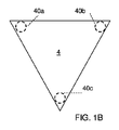
図1A,図1B及び図1Cは、それぞれサブマウント1と、電子部品4と、サブマウント1に結合した電子部品4の組立品5とを示している。
1A, 1B, and 1C show a
サブマウント1は、電子部品4をキャリヤ6に電気的及び機械的に連結するのに役立つ(図2参照)。サブマウント1は、サブマウントにキャリヤに取り付けるための取付部10と、電子部品4を固定するための付着部12a,12b,12cとを有する。さらに、サブマウント1は、キャリヤの各導体と接続(協調)するための第1の電気接触部14a,14bと、電子部品4の各電気接触部40a,40b,40cと接続(協調)するための第2の電気接触部16a,16b,16cとを有する。第2の電気接触部16a,16b,16cは、それぞれ電気的に第1の電気接触部14a,14bに接続される。この場合、第2の電気接触部16a,16bは両方とも、電気的な接続15a,15bを介して第1の電気接触部14aに接続され、第2の電気接触部16cは、接続15cを介して第1の電気接触部14bに電気的に接続される。付着部12a,12b,12cは、各延長部18a,18b,18cによって取付部10に結合され、各延長部18a,18b,18cは取付部20から離れる方向に付着部12a,12b,12cが変位できるように取付部20によって定義される平面(図面のなす平面に相当)内において横方向に伸縮自在である。電気的な接続15a,15b,15cは、実線で概略的に示される。しかしながら、これらの電気的な接続はいかなる形状も取り得る。第2及び第1の電気接触部の間に低インピーダンス接続を提供するために、電気的な接続は延長部の全幅に及んでいることが好ましい。しかし、いくつかの種類の電子部品のために、延長部は一つ以上の電気的な接続を有していることが望ましい。一部の例では、電気的な接続は、抵抗として作用するように比較的小さい幅を有することが好ましい。
The
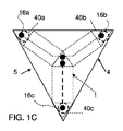
図1Bは、例えば太陽電池や発光部品などの電子部品4を概略的に示している。この電子部品は、サブマウントに付着される裏面上に各電気的なデバイス接触部40a,40b,40cを有する。図1Cは、サブマウント1と結合した電子部品4の組立品5を示している。サブマウントの第2の電気接触部16a,16b,16cは、電子部品4の各電気的なデバイス接触部40a,40b,40cに電気的に接続される。サブマウント1の第2の電気接触部16a,16b,16cと電子部品4のデバイス接触部40a,40b,40cとの間の電気的な接続は、例えば導電性の接着剤によって実施される。導電性の接着剤は、さらにサブマウント1と電子部品4の機械的な結合も与えることができる。
FIG. 1B schematically shows an
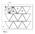
図2は、それぞれ電子部品4を固定するサブマウント1を備えた複数の組立品5a,5b,5c,5d・・・を有するキャリヤ6の組立品を示している。この図面が不明瞭とならないように組立品5a,5bだけは詳細に図示している。
FIG. 2 shows an assembly of the
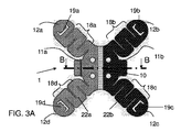
図3Aは、サブマウント1の現在の好ましい実施形態を示している。図3Bは、図3AのB−B断面図を示している。現在の好ましい実施形態のサブマウント1は、金属層22でコーティングされたポリマーホイル20から一体形成される。例えばポリマーホイル20は、厚さ125μmのPENホイルであり、金属層は、厚さ15μmの銅層である。なお、サブマウントに必要な剛性及び柔軟性によっては、他の材質にしたり、他の厚さにしたりしてもよい。図3Bに示すように、金属層22は、1つ目の第1の電気接触部14aを有する第1の導電性領域と、2つ目の第1の電気接触部14bを有する第2の導電性領域と、を提供するために局所的に遮断されている。本実施形態では、サブマウントの延長部は蛇行形状を有する。この場合、延長部を伸縮性の材料で形成する必要はない。延長部の材料が柔軟性材料であれば十分である。例えばPETやPEN等のほとんどのポリマーホイルはこの条件を満たしている。このことは、サブマウントの異なる部分の機械的特性がそれらの形状によって十分に定義されるという長所を有する。また、サブマウントが特定の種類のホイルから一体形成されていても、取付部及び付着部は比較的剛性を有し、延長部は伸縮可能とすることができる。
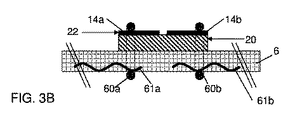
FIG. 3A shows a presently preferred embodiment of the
本実施形態のサブマウント1は、伸縮可能な独立した蛇行部18a〜18dが形成されるように、レーザー切断され、打ち抜きされ、又は切断されることによって成形される。これらの蛇行部は一度伸ばされるとバネのように作用する。このバネは、例えばホイルの4つの端部を折ることにより、図5B〜図5Eにおいて詳細に示すようにクランプされたとき、インターポーザーの中央に電子部品を保持することができる。電子部品の領域をインターポーザーの寸法に合わせると、バネに加わる力がセットされる。
The
図3Bに示すように、この例では、サブマウント1が、一対の導電性ワイヤ60a,60bによってキャリヤ6へのリップ部11a,11bに取り付けられる。これらのワイヤ60a,60bは、サブマウント1をキャリヤ6に機械的に結合させる。また、ワイヤ60a,60bはそれぞれサブマウント1の各導電性領域14a,14bをキャリヤ6の各導電体61a,61bに電気的に接続する。
As shown in FIG. 3B, in this example, the
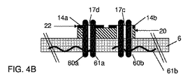
図4Aと図4Bは、図3Aと図3Bの実施形態の変形例を示している。図4Bは、図4AのB−B断面図を示している。図4Bの断面図は、明確さのために拡大して示している。図4Aと図4Bの実施形態では、サブマウント1は、取付部10の開口部17a,17b,17c,17dを介して導電性ワイヤ60a,60bによってキャリヤに縫い付けられている。
4A and 4B show a variation of the embodiment of FIGS. 3A and 3B. FIG. 4B shows a BB cross-sectional view of FIG. 4A. The cross-sectional view of FIG. 4B is shown enlarged for clarity. 4A and 4B, the
部品の織編物等のキャリヤに対する他の取付方法や電気的な接続方法は、上述した国際公開第2008/007237号及び国際公開第2011/093713号に記載されている。 Other attachment methods and electrical connection methods for a carrier such as woven or knitted parts are described in the above-mentioned International Publication Nos. 2008/007237 and 2011/0993713.
図3A,図3B,図4A,図4Bに示すサブマウント1の実施形態では、付着部12a,12b,12c,12dが内向きホック(pointing hook)の形態の各把持部19a,19b,19c,19dを備えることを特徴とする。
In the embodiment of the
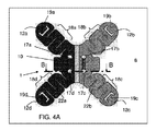
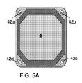
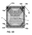
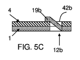
図5Aは、サブマウント1に組み込まれるのに適した電子部品4を示している。電子部品4は、OLEDや太陽電池等であり、例えば図3A,図3B,図4A,図4Bに示すように、サブマウント1の把持要素19a,19b,19c,19dと協調する開口部42a,42b,42c,42dを有している。これらを有して得られた組立品は、図5Bにおいて概略的に図示されている。この組立品において、ホック19a,19b,19c,19dは、電子部品4の開口部42a,42b,42c,42dを通って延びている。延長部18a〜18dは、ホック19a〜19dに対して半径方向内向きの力を作用し、電子部品4への十分な把持力を維持する。このようにして得られた接続は、図5BのC−C断面図である図5Cに概略的に図示されている。
FIG. 5A shows an
まず、延長部18a〜18dを外側に引き延ばして電子部品4をサブマウント1に適用し、ホック19a〜19dが電子部品の開口部42a〜42dを貫通するように延長部18a〜18dを緩ませることによって、電子部品4がサブマウント1に取り付けられる。実施形態の電子部品4は、いずれかのホック、例えばホック19bが対応する開口部42bを貫通するように、サブマウント1上に置かれる。その後、サブマウント1の平面内において電子部品4に力を作用させて、各ホックの前に電子部品4の別の開口部を配置し、当該ホックが電子部品4の各開口部に入るようにする。これは、電子部品4が十分にサブマウント1に結合されるまで繰り返される。電子部品4が損傷しやすい場合には、これらの配置動作中の損傷は、電子部品4の表面上に対して略一様な吸引力を有する吸引グリッパを用いて電子部品を配置することによって予防することができる。
First, the
サブマウント1と電子部品4との間の電気的な接続は、サブマウント1の付着部12a〜12dの位置でサブマウント1に面している部品の一端で電気的に接触させることにより形成される。延長部18a〜18dによって与えられたクランプ力により、サブマウントの付着部12a〜12dによって形成された電気的な接触部に対して部品の電気的な接触部を押し当てる。
The electrical connection between the
サブマウントの把持要素19a〜19dと開口部42a〜42dとの間の協調によって形成された機械的な接続は、粘着剤によって補強することができる。この粘着剤は、電子部品4とサブマウント1との間の電気的な接続も補強するように導電性の接着剤を使用することが好ましい。
The mechanical connection formed by the cooperation between the submount
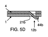
図5Dは、図5Cと同様の断面における変形例を示し、電子部品が、サブマウント1の付着部における開口部(例えば開口部21b)と協調する半径方向外向きのホック(例えばホック44b)を有することを特徴とする。この場合、開口部21bが把持要素を形成する。
FIG. 5D shows a modification in the same cross section as FIG. 5C, in which the electronic component has a radially outward hook (for example, a
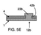
図5Eは、さらに図5Cと同様の断面における変形例を示し、サブマウント1の付着部が、電子部品4の開口部(例えば開口部42b)にスナップ留めされる(はめ込まれる)突起(例えば突起23b)を有していることを特徴とする。
5E further shows a modified example in the same cross section as FIG. 5C, in which the attachment portion of the
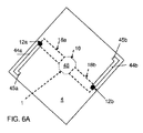
図6Aと図6Bは、サブマウント1と、サブマウント1の電子部品4との組立品の別の実施形態を示している。サブマウント1の電子部品4の背後に隠れた部分は、破線で示されている。本実施形態において、電子部品は、それぞれ端部45a,45bを有するスリット44a,44bを有している。端部45a,45bに向かう方向において、スリット44a,44bは、電子部品4の中央位置46から第1の距離に渡って離れて延びていて、更に、スリット44a,44bは、端部45a,45bにおいて中央に向かって、第1の距離より小さい、第2の距離に渡って延びている。
6A and 6B show another embodiment of the assembly of the
図6Aは、電子部品4がサブマウント1上にどのように初期配置されるかを示し、付着部12aは、スリットの端部45aの反対側のスリット44aの端部の前に配置されている。同様に、付着部12bは、スリット44bの端部45bの反対側のスリット44bの端部の前方に配置されている。また、突起(例えば付着部12a,12bのホック)がスリット44a,44bを通って延びている。
FIG. 6A shows how the
その後、付着部12a,12bで形成された突起を固定したまま、電子部品4は時計方向に45度に渡って回転する。また、図6Bに示すように、スリット44a,44bの端部45a,45bに延長部の突起がスナップ留めされるとき、延長部18a,18bが伸びてわずかに緩む。
Thereafter, the
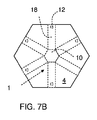
図7Aと図7Bは、電子部品4と組み合わされたサブマウント1の他の一例を示している。図7Aの実施形態では、サブマウント1は、それぞれ付着部12a,12bを有する延長部18a,18bのみを有している。図7Bの実施形態では、サブマウント1は、それぞれ付着部12を有する6つの延長部18を有している
7A and 7B show another example of the
実施形態において、サブマウントは、取付部によって定義される平面における回転に対して非対称とすることができる。この場合、その平面における方向付けを速やかに決定することができる。これは、電気的にキャリヤに接続する場合に重要となる部品の取付けに特に有利である。 In an embodiment, the submount can be asymmetric with respect to rotation in a plane defined by the attachment. In this case, the orientation in the plane can be determined quickly. This is particularly advantageous for mounting components that are important when electrically connected to a carrier.
図8は、例えば図2に示される各サブマウント1と共に、キャリヤ6に付着される電子部品4を備えるキャリヤ6を製造するための製造装置の配列を概略的に図示している。製造装置の配列は、キャリヤ6を製造する第1の製造ライン110と、サブマウント1を製造する第2の製造ライン120と、電子部品4を製造する製造ライン130と、を備える。製造装置の配列は、さらに、サブマウント1とキャリヤ6を組み立てる第1の組立ステーション140と、電子部品4と各サブマウント1を組み立てる第2の組立ステーション150と、を備える。
FIG. 8 schematically illustrates an arrangement of a manufacturing apparatus for manufacturing a
動作中に、製造装置の配列は、各サブマウント1と共に、キャリヤ6に付着される電子部品4を備えるキャリヤ6を製造する製造処理を実行する。製造工程は、キャリヤ6を製造する第1の処理工程S10と、サブマウント1を製造する第2の処理工程S20と、電子部品4を製造する第3の処理工程S30と、を備える。製造処理は、さらに、サブマウント1とキャリヤ6を組み立てる第1の組立工程S40と、各サブマウント1と電子部品を組み立てる第2の組立工程S50と、を備える。
During operation, the manufacturing apparatus arrangement performs a manufacturing process for manufacturing the
キャリヤ6は、導電性を有する織編物を製造する公知の処理S10等の公知の処理によって製造することができる。電子部品4は、OLED,太陽光発電素子または太陽電池を製造する処理などの公知の処理S30等によって製造することができる。
The
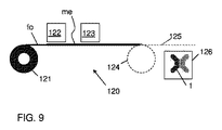
図9は、本発明の実施形態にかかるサブマウント1を製造する製造ライン120を概略的に図示している。
FIG. 9 schematically shows a
本実施形態の製造ライン120は、ポリマーホイルfo(例えばPEN又はPETホイル)を供給する供給ロール121を備える。製造ライン120は、さらに、金属層meをホイル上に堆積させる堆積ステーション122を備える。また、例えば図1A,図3A,図6A,図7A,又は図7Bに示すように、製造ライン120は、そのホイルをサブマウントが要求する形状となるようにパターン形成するパターン形成ステーション123を備える。パターン形成ステーション123は、堆積された金属層meを、相互に絶縁された領域、例えば領域22a,22b(図4A)となるようにパターン形成してもよい。また、堆積ステーション122は、すでに望ましいパターンに従って金属層meを堆積させておくこともできる。製造ライン120は、さらにホイルfoからサブマウント1を分離する分離ステーション(不図示)を有していてもよい。また、パターン形成ステーション123は、サブマウント1を分離するものであってもよい。実施形態では、この製造ラインにおいてサブマウント1はホイルfoから分離されていないが、例えば、わずかな深さまでホイルを除去したり、又はドットパターンに応じてその外形に沿ってホイルに穿孔したりする等、部分的にホイルfoをカットすることにより、ホイルは形成すべきサブマウント1の外形に沿って弱くなる。この場合、サブマウント1は、製造処理の後の段階で、ホイルfoから除去することができる。この場合、ホイルfoは、収納ロール124上に巻き取らせることができ、又はさらなる処理のために移送手段125で移送することができる。完成したサブマウント1は、収納箱126に収納することができ、又は移送手段125によって移送することができる。ホイルfoのパターン形成は、機械的な切削工具で実施することができる。しかしながら、ホイルはレーザーパターン形成ステーションによってパターン形成されることが好ましい。この場合、パターン形成ステーションとホイルfo及び/又は金属層meとの間の物理的な接触はない。これは、ホイルの連続的な移送を可能にする。
The
組立ステーション140は、例えば国際公開第2011/093713号に示されているような公知の方法によってサブマウント1とキャリヤ6を組み立てる。
The
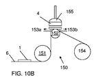
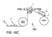
図10は、電子部品4とそれらのサブマウント1を組み立てる組立ステーション150の実施形態を概略的に図示している。図10Aは、図10の視点Aから見た状態を詳細に示している。図10の組立ステーションでは、サブマウント1を備えたキャリヤ6が提供され、その2つだけが明確化のために示されている。キャリヤ6は、誘導ロール151を通って、サブマウント1を運搬する側でキャリヤ6を凸状に曲げるキャリヤ曲げロール152の方へ移送される。サブマウント1は、自身の取付部10がキャリヤ6に取り付けられるだけなので、付着部12a〜12dとなって終わる延長部18a〜18dは、弾性的にキャリヤ6の表面から離れる。この状態のサブマウントでは、引き延ばし用具153a,153b,153c,153dは、各付着部12a,12b,12c,12dの中に把持し、図10Aに矢印で示すように、対応する延長部18a,18b,18c,18dを取付部10から離れる横方向に引き延ばす。これにより、引き延ばし用具153a,153b,153c,153dは、ホック19a〜19dを上方に、すなわちキャリヤ6から離れる方向に押し上げる。図10Bに示すように、この延長状態の延長部18a〜18dにおいて、配置装置155は、例えば、図5C,図5D及び図5Eに示すように、サブマウント1の付着部が取り付けられる電子部品4の対応する付着部の中に把持するように、電子部品4をサブマウント1上に配置する。その後、引き延ばし用具153a〜153dは、図10Cに示すように、電子部品4がサブマウント1に固定されたままの状態で、サブマウントを解放する。その後、サブマウント1を有するキャリヤ6は、収納ロール154に移送される。
FIG. 10 schematically illustrates an embodiment of an
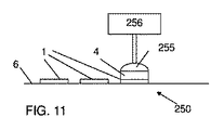
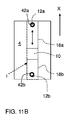
図11は、電子部品4をサブマウント1に組み込む別の配置の組立ステーション250を示している。この実施形態では、組立ステーション250は、サブマウント1上に初期配置された後に電子部品4を横方向に変位する配置用具255を有する。
FIG. 11 shows another arrangement of the
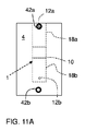
図11Aは、例えば図5C,図5D,図5Eに詳細を示すように、サブマウント1の付着部の1つ12aを、電子部品4の付着部の各1つ42aに協調させることができるように初期配置された部品4を示している。
In FIG. 11A, for example, as shown in detail in FIGS. 5C, 5D, and 5E, one
図11Bは、配置装置255を変位する変位装置256によって生じる方向Xにおいて、電子部品4の横方向の変位の影響を示している。これは、電子部品4に結合された付着部12aを有する延長部18aがその方向に引き延ばされるようにするので、電子部品4の付着部42bは、サブマウントの対応する付着部12bに対向して配置され、これらの付着部12b,42bは互いにスナップ留めすることができる。
FIG. 11B shows the influence of the lateral displacement of the
その後、電子部品4は配置用具255によって解放される。ここでは、取付部に延長部を伴って結合された2つの付着部を有するサブマウント1のための原理が示されているが、この方法は、より複雑なサブマウントについても同様に適用可能である。例えば、図7Bに示されるサブマウント1のために、電子部品4は、初期配置の後に5つの横方向の変位を使用するサブマウントに接続することができ、その接続が付着部の1つとそれに対応するサブマウントの付着部の間でなされることを特徴とする。
Thereafter, the
例えば対応するサブマウント1及び電子部品4の付着部12a,42bが、スナップ留め動作によって本質的に協調する必要はない。また、相互に対応する付着部は、互いに接着する表面であってもよい。この接着のために、例えばUV硬化型の接着剤のように早く硬化する接着剤を使用してもよい。図10の実施形態において、引き延ばし用具153a〜153dは延長部18a〜18dを延長した位置に維持し、その間、配置用具155は接着剤が硬化するまでに電子部品4を維持するため、このことが実現できる。
For example, the
図11の実施形態において、付着部12a,42aを付着させるための接着剤が硬化するまで、配置用具255によって生じる横方向の変位が延期されるため、このことが実現できる。さらに、配置用具255は、付着部12b,42bを付着させるための接着剤が硬化するまで部品4を固定した状態を維持すべきである。部品4がサブマウント1の各付着部への2つ以上の付着部を伴って付着される場合には、配置用具255は、付着部12a,42aに対応する一式の各付着部の接着剤が硬化するまでの各時間において、部品4を固定した状態を維持すべきである。
In the embodiment of FIG. 11, this can be achieved because the lateral displacement caused by the
本発明は、特に、サブマウントが電子部品を織編物に電気的に結合させるために使用されることを特徴とする応用のために記載している。しかしながら、このサブマウントは、電子部品をゴム製等の異なる種類のキャリヤに結合させる場合でも同様に適用可能である。いかなる場合であっても、サブマウントは比較的より伸縮性のキャリヤに比較的剛性の電子部品を取り付けることを可能とする。 The invention is described in particular for applications characterized in that the submount is used to electrically couple the electronic component to the knitted fabric. However, this submount can be similarly applied even when the electronic component is coupled to a different type of carrier such as rubber. In any case, the submount allows a relatively rigid electronic component to be attached to a relatively more stretchable carrier.
特許請求の範囲において「備え(comprising)」という用語は、他の要素や工程を排除するものではなく、不定冠詞「a」又は「an」は複数を排除するものではない。単一の構成要素又はその他の単位は、特許請求の範囲に記載されているいくつかの事項の機能を満たすことができる。特定の手段が相互に異なる請求項に記載されているという単なる事実は、これらの手段の組み合わせが有利に使用できないことを示すものではない。特許請求の範囲におけるいかなる参照符号も、その範囲を限定するものとして解釈されるべきではない。 In the claims, the term “comprising” does not exclude other elements or steps, and the indefinite article “a” or “an” does not exclude a plurality. A single component or other unit may fulfill the functions of several items recited in the claims. The mere fact that certain measures are recited in mutually different claims does not indicate that a combination of these measured cannot be used to advantage. Any reference signs in the claims should not be construed as limiting the scope.
Claims (12)
当該サブマウントを前記キャリヤに取付けるための取付部(10)と、
前記電子部品を固定するための付着部(12a,12b,12c,12d)と、
前記キャリヤの各導体(61a,61b)と協調するための第1の電気的接触部(14a,14b)と、
前記電子部品の各電気的接触部と協調するための、第1の電気的接触部に電気的に接続される、第2の電気的接触部(16a,16b,16c)と、を備え、
前記付着部は各延長部(18a,18b,18c)によって前記取付部に連結され、
前記延長部は、前記取付部から離れる方向に前記付着部が変位できるように、前記取付部によって定義される平面上において横方向に伸縮可能となっており、
前記付着部(12a,12b,12c,12d)が把持要素(19a,19b,19c,19d)を備える、
ことを特徴とするサブマウント(1)。 A submount (1) for mechanically and electrically connecting an electronic component (4) to a carrier (6),
An attachment portion (10) for attaching the submount to the carrier;
Adhering portions (12a, 12b, 12c, 12d) for fixing the electronic components;
A first electrical contact (14a, 14b) for cooperating with each of the conductors (61a, 61b) of the carrier;
A second electrical contact portion (16a, 16b, 16c) electrically connected to the first electrical contact portion for coordinating with each electrical contact portion of the electronic component;
The attachment portion is connected to the attachment portion by each extension portion (18a, 18b, 18c),
The extension portion, the so said attachment in a direction away from the mounting portion can be displaced, has a stretchable in the transverse direction on the plane defined by the mounting portion,
The attachment part (12a, 12b, 12c, 12d) includes a gripping element (19a, 19b, 19c, 19d).
Submount (1) characterized by the above.
ことを特徴とする請求項1に記載のサブマウント。 The submount (1) is integrally formed from a polymer foil (fo).
The submount according to claim 1, wherein:
前記金属層は、前記第2の電気的接触部(16a,16b,16c)とそれらに対応する前記第1の電気的接触部(14a,14b)との間の電気的な接続(15a,15b,15c)を形成している、
ことを特徴とする請求項2に記載のサブマウント。 The polymer foil (fo) is coated with a metal layer (me),
The metal layer has electrical connections (15a, 15b) between the second electrical contacts (16a, 16b, 16c) and the corresponding first electrical contacts (14a, 14b). , 15c),
The submount according to claim 2, wherein:
ことを特徴とする請求項1に記載のサブマウント。 The extensions (18a, 18b, 18c, 18d) have a serpentine shape;
The submount according to claim 1, wherein:
ことを特徴とする請求項1に記載のサブマウント。 Asymmetric with respect to rotation of the mounting portion (10) in the plane;
The submount according to claim 1, wherein:
電子部品(4)を提供する工程(S30)と、
前記電子部品(4)を前記サブマウント(1)の付着部(12a,12b,12c,12d)に付着する工程(S50)と、
を備え、
前記各付着部(12a,12b,12c,12d)が把持要素(19a,19b,19c,19d)を備え、
少なくとも1つの前記延長部(18a,18b,18c,18d)を引き延ばし、前記電子部品(4)を前記サブマウント(1)上に配置し、少なくとも1つの前記延長部を少なくとも部分的に緩ませて、前記付着部を前記電子部品の各付着部(42a,42b,42c,42d)に把持させることによって、前記電子部品を前記付着部に付着させる(S50)、
ことを特徴とする組立方法。 Providing a carrier (6) having at least one submount (1) according to claim 1 (S10, S20, S40);
Providing an electronic component (4) (S30);
Attaching the electronic component (4) to the attachment portions (12a, 12b, 12c, 12d) of the submount (1) (S50);
Equipped with a,
Each of the attachment portions (12a, 12b, 12c, 12d) includes a gripping element (19a, 19b, 19c, 19d),
Extending at least one of the extensions (18a, 18b, 18c, 18d), placing the electronic component (4) on the submount (1) and at least partially loosening at least one of the extensions; The electronic part is attached to the attachment part by gripping the attachment part to each attachment part (42a, 42b, 42c, 42d) of the electronic part (S50),
Assembly how to, characterized in that.
前記キャリヤは、湾曲した表面(152)上に案内されて、前記キャリヤと前記サブマウント(1)の前記付着部(12a,12b,12c,12d)との間に間隔を与え、
前記間隔内に引き延ばし用具(153a,153b,153c,153d)を挿入し、前記延長部を前記引き延ばし用具によって引き延ばし、前記電子部品(4)を置き、前記延長部を解放することによって、前記付着部を前記電子部品の各付着部にスナップ留めする、
ことを特徴とする請求項8に記載の組立方法。 The carrier (6) is formed from a flexible material;
The carrier is guided on a curved surface (152) to provide a spacing between the carrier and the attachment (12a, 12b, 12c, 12d) of the submount (1);
The extension part (153a, 153b, 153c, 153d) is inserted in the interval, the extension part is extended by the extension tool, the electronic component (4) is placed, and the extension part is released, thereby the attachment part. Are snapped to each attachment part of the electronic component,
The assembling method according to claim 8 , wherein:
前記電子部品に力を与えることによって、前記付着部に対応する前記延長部(18a)を引き延ばすと共に、前記電子部品の前記付着部の少なくとも1つの第2の付着部(42b)が、前記サブマウントの他の各付着部(12b)内に把持される、
ことを特徴とする請求項8に記載の組立方法。 The electronic component (4) is disposed at a position where the attachment portion (42) of at least one electronic component (4) cooperates with each attachment portion (12a) of the submount (1),
By applying a force to the electronic component, the extension portion (18a) corresponding to the attachment portion is extended, and at least one second attachment portion (42b) of the attachment portion of the electronic component is the submount. Gripped in each of the other attachments (12b),
The assembling method according to claim 8 , wherein:
前記電子部品を少なくとも1つの前記サブマウントに付着させる付着設備と、
前記電子部品を前記少なくとも1つのサブマウントに付着させながら、少なくとも1つの前記延長部(18a)を引き延ばした状態に維持する設備と、を備える、
ことを特徴とする組立装置(150)。 An assembly device for combining an electronic component (4) with a carrier (6) having at least one submount (1) according to claim 1,
An attachment facility for attaching the electronic component to at least one of the submounts;
A facility for maintaining at least one extension (18a) in an extended state while attaching the electronic component to the at least one submount.
An assembly apparatus (150) characterized by the above.
ことを特徴とする請求項11に記載の組立装置。 The facility for maintaining at least one of the extensions in an extended state is a displacement device (256) that laterally displaces the attachment facility (255).
The assembly apparatus according to claim 11 .
Applications Claiming Priority (3)
| Application Number | Priority Date | Filing Date | Title |
|---|---|---|---|
| EP12159639.9 | 2012-03-15 | ||
| EP12159639.9A EP2640168A1 (en) | 2012-03-15 | 2012-03-15 | Submount, assembly including submount, method of assembling and assembling device |
| PCT/NL2013/050172 WO2013137732A1 (en) | 2012-03-15 | 2013-03-14 | Submount, assembly including submount, method of assembling and assembling device |
Publications (2)
| Publication Number | Publication Date |
|---|---|
| JP2015516676A JP2015516676A (en) | 2015-06-11 |
| JP6231069B2 true JP6231069B2 (en) | 2017-11-15 |
Family
ID=47997737
Family Applications (1)
| Application Number | Title | Priority Date | Filing Date |
|---|---|---|---|
| JP2015500376A Expired - Fee Related JP6231069B2 (en) | 2012-03-15 | 2013-03-14 | Submount, assembly including submount, assembly method, and assembly apparatus |
Country Status (5)
| Country | Link |
|---|---|
| US (1) | US9474155B2 (en) |
| EP (2) | EP2640168A1 (en) |
| JP (1) | JP6231069B2 (en) |
| CN (1) | CN104303604B (en) |
| WO (1) | WO2013137732A1 (en) |
Families Citing this family (11)
| Publication number | Priority date | Publication date | Assignee | Title |
|---|---|---|---|---|
| EP2640168A1 (en) | 2012-03-15 | 2013-09-18 | Nederlandse Organisatie voor toegepast-natuurwetenschappelijk Onderzoek TNO | Submount, assembly including submount, method of assembling and assembling device |
| US9674949B1 (en) | 2013-08-27 | 2017-06-06 | Flextronics Ap, Llc | Method of making stretchable interconnect using magnet wires |
| US10231333B1 (en) | 2013-08-27 | 2019-03-12 | Flextronics Ap, Llc. | Copper interconnect for PTH components assembly |
| WO2015033736A1 (en) * | 2013-09-05 | 2015-03-12 | 株式会社村田製作所 | Multilayer substrate |
| US9521748B1 (en) | 2013-12-09 | 2016-12-13 | Multek Technologies, Ltd. | Mechanical measures to limit stress and strain in deformable electronics |
| US9338915B1 (en) * | 2013-12-09 | 2016-05-10 | Flextronics Ap, Llc | Method of attaching electronic module on fabrics by stitching plated through holes |
| EP3251473B1 (en) * | 2015-01-27 | 2018-12-05 | Nederlandse Organisatie voor toegepast- natuurwetenschappelijk onderzoek TNO | Flexible device module for fabric layer assembly and method for production |
| JP6712764B2 (en) * | 2015-05-25 | 2020-06-24 | パナソニックIpマネジメント株式会社 | Stretchable flexible substrate and manufacturing method thereof |
| US20170181276A1 (en) * | 2015-12-21 | 2017-06-22 | Panasonic Intellectual Property Management Co., Ltd. | Substrate including stretchable sheet |
| FI127173B (en) | 2016-09-27 | 2017-12-29 | Tty-Säätiö Sr | Extensible construction comprising a conductive path and method of manufacturing the structure |
| DE102018104169A1 (en) * | 2018-02-23 | 2019-08-29 | Osram Opto Semiconductors Gmbh | Opto-electronic assembly, process and molding |
Family Cites Families (26)
| Publication number | Priority date | Publication date | Assignee | Title |
|---|---|---|---|---|
| BE1007618A3 (en) * | 1993-10-13 | 1995-08-22 | Philips Electronics Nv | Flexible mounting body and object with such confirmation body support with an object and such confirmation body and package with some of such confirmation bodies. |
| JPH08264673A (en) * | 1995-03-22 | 1996-10-11 | Oki Electric Ind Co Ltd | Integrated circuit device |
| US6743982B2 (en) * | 2000-11-29 | 2004-06-01 | Xerox Corporation | Stretchable interconnects using stress gradient films |
| DE10260646A1 (en) * | 2002-12-23 | 2004-07-08 | Infineon Technologies Ag | Housing for semiconducting components has base surface essentially in form of triangle and housing essentially in form of triangular prism; all lateral surfaces can have connecting elements |
| US7491892B2 (en) * | 2003-03-28 | 2009-02-17 | Princeton University | Stretchable and elastic interconnects |
| GB2416621A (en) | 2004-07-27 | 2006-02-01 | Cambridge Display Tech Ltd | Laminated interconnects for opto-electronic device modules |
| US8084117B2 (en) * | 2005-11-29 | 2011-12-27 | Haresh Lalvani | Multi-directional and variably expanded sheet material surfaces |
| JP5113160B2 (en) * | 2006-06-08 | 2013-01-09 | コーニンクレッカ フィリップス エレクトロニクス エヌ ヴィ | Submount for placement of electronic components and placement including submount |
| WO2008084412A1 (en) | 2007-01-05 | 2008-07-17 | Philips Intellectual Property & Standards Gmbh | Reinforced organic light emitting diode |
| DE102007014477A1 (en) * | 2007-03-22 | 2008-09-25 | Rent-A-Scientist Gmbh | Method for fastening electrically conductive thread to textile fabric, wherein electrically conductive thread is used as reel thread and fastening is carried out in form of two-thread lock stitch seam |
| EP2255378B1 (en) * | 2008-03-05 | 2015-08-05 | The Board of Trustees of the University of Illinois | Stretchable and foldable electronic devices |
| EP2289291A1 (en) | 2008-06-10 | 2011-03-02 | Koninklijke Philips Electronics N.V. | Electronic textile |
| US8207473B2 (en) * | 2008-06-24 | 2012-06-26 | Imec | Method for manufacturing a stretchable electronic device |
| SG160245A1 (en) * | 2008-09-12 | 2010-04-29 | Dragon Energy Pte Ltd | A base tile |
| WO2010058360A1 (en) * | 2008-11-21 | 2010-05-27 | Koninklijke Philips Electronics N.V. | Textile electronic arrangement |
| JP2012511811A (en) | 2008-12-09 | 2012-05-24 | コーニンクレッカ フィリップス エレクトロニクス エヌ ヴィ | Flexible modular assembly |
| WO2010086033A1 (en) * | 2009-01-30 | 2010-08-05 | Interuniversitair Microelektronica Centrum Vzw | Stretchable electronic device |
| EP2392196B1 (en) * | 2009-01-30 | 2018-08-22 | IMEC vzw | Stretchable electronic device |
| WO2010086416A1 (en) * | 2009-01-30 | 2010-08-05 | Imec | Stretchable electronic device |
| US8332053B1 (en) * | 2009-04-28 | 2012-12-11 | Hrl Laboratories, Llc | Method for fabrication of a stretchable electronic skin |
| DE102009031568A1 (en) * | 2009-06-29 | 2010-12-30 | Fraunhofer-Gesellschaft zur Förderung der angewandten Forschung e.V. | Method for producing an electronic system, method for producing a free-form surface with such a system, as well as electronic system and free-form surfaces with such a system |
| US8883287B2 (en) * | 2009-06-29 | 2014-11-11 | Infinite Corridor Technology, Llc | Structured material substrates for flexible, stretchable electronics |
| JP2011077139A (en) * | 2009-09-29 | 2011-04-14 | Panasonic Electric Works Co Ltd | Circuit module and method for mounting the same |
| US8732866B2 (en) * | 2009-11-20 | 2014-05-27 | Ryan T. Genz | Fabric constructions with sensory transducers |
| EP2529606A1 (en) | 2010-01-29 | 2012-12-05 | Nederlandse Organisatie voor toegepast- natuurwetenschappelijk onderzoek TNO | Tile, assembly of tiles with a carrier, method of manufacturing an assembly |
| EP2640168A1 (en) | 2012-03-15 | 2013-09-18 | Nederlandse Organisatie voor toegepast-natuurwetenschappelijk Onderzoek TNO | Submount, assembly including submount, method of assembling and assembling device |
-
2012
- 2012-03-15 EP EP12159639.9A patent/EP2640168A1/en not_active Withdrawn
-
2013
- 2013-03-14 EP EP13712380.8A patent/EP2826346B1/en not_active Not-in-force
- 2013-03-14 US US14/385,071 patent/US9474155B2/en not_active Expired - Fee Related
- 2013-03-14 CN CN201380023261.9A patent/CN104303604B/en not_active Expired - Fee Related
- 2013-03-14 WO PCT/NL2013/050172 patent/WO2013137732A1/en not_active Ceased
- 2013-03-14 JP JP2015500376A patent/JP6231069B2/en not_active Expired - Fee Related
Also Published As
| Publication number | Publication date |
|---|---|
| EP2826346B1 (en) | 2018-10-31 |
| EP2826346A1 (en) | 2015-01-21 |
| CN104303604A (en) | 2015-01-21 |
| EP2640168A1 (en) | 2013-09-18 |
| JP2015516676A (en) | 2015-06-11 |
| US9474155B2 (en) | 2016-10-18 |
| WO2013137732A1 (en) | 2013-09-19 |
| US20150041201A1 (en) | 2015-02-12 |
| CN104303604B (en) | 2017-04-05 |
Similar Documents
| Publication | Publication Date | Title |
|---|---|---|
| JP6231069B2 (en) | Submount, assembly including submount, assembly method, and assembly apparatus | |
| US11617268B2 (en) | Fabric with embedded electrical components | |
| EP2030493B1 (en) | Submount for electronic components | |
| US9078361B2 (en) | Assembly, component for an assembly and method of manufacturing an assembly | |
| US20170059140A1 (en) | Method and system for a three-dimensional (3-d) flexible light emitting diode (led) bar | |
| TWI352179B (en) | Light module | |
| US10772197B2 (en) | Electronically functional yarn | |
| US10368436B2 (en) | Conductor pad for flexible circuits and flexible circuit incorporating the same | |
| WO2010058360A1 (en) | Textile electronic arrangement | |
| EP3251473B1 (en) | Flexible device module for fabric layer assembly and method for production | |
| US20190085487A1 (en) | Electronically functional yarn and textile | |
| JP5644024B2 (en) | Flexible printed wiring board, lighting device and manufacturing method thereof | |
| CN112640589A (en) | Electronic device and method for manufacturing the same | |
| JP2011040929A (en) | Electrostatic speaker and method of manufacturing the same |
Legal Events
| Date | Code | Title | Description |
|---|---|---|---|
| A621 | Written request for application examination |
Free format text: JAPANESE INTERMEDIATE CODE: A621 Effective date: 20160222 |
|
| A131 | Notification of reasons for refusal |
Free format text: JAPANESE INTERMEDIATE CODE: A131 Effective date: 20170418 |
|
| A601 | Written request for extension of time |
Free format text: JAPANESE INTERMEDIATE CODE: A601 Effective date: 20170714 |
|
| A521 | Request for written amendment filed |
Free format text: JAPANESE INTERMEDIATE CODE: A523 Effective date: 20170905 |
|
| TRDD | Decision of grant or rejection written | ||
| A01 | Written decision to grant a patent or to grant a registration (utility model) |
Free format text: JAPANESE INTERMEDIATE CODE: A01 Effective date: 20170919 |
|
| A61 | First payment of annual fees (during grant procedure) |
Free format text: JAPANESE INTERMEDIATE CODE: A61 Effective date: 20171018 |
|
| R150 | Certificate of patent or registration of utility model |
Ref document number: 6231069 Country of ref document: JP Free format text: JAPANESE INTERMEDIATE CODE: R150 |
|
| LAPS | Cancellation because of no payment of annual fees |