JP6223055B2 - Photoelectric conversion device - Google Patents
Photoelectric conversion device Download PDFInfo
- Publication number
- JP6223055B2 JP6223055B2 JP2013167683A JP2013167683A JP6223055B2 JP 6223055 B2 JP6223055 B2 JP 6223055B2 JP 2013167683 A JP2013167683 A JP 2013167683A JP 2013167683 A JP2013167683 A JP 2013167683A JP 6223055 B2 JP6223055 B2 JP 6223055B2
- Authority
- JP
- Japan
- Prior art keywords
- photoelectric conversion
- conversion unit
- unit
- signal
- conductivity type
- Prior art date
- Legal status (The legal status is an assumption and is not a legal conclusion. Google has not performed a legal analysis and makes no representation as to the accuracy of the status listed.)
- Expired - Fee Related
Links
Images


Classifications
-
- H—ELECTRICITY
- H04—ELECTRIC COMMUNICATION TECHNIQUE
- H04N—PICTORIAL COMMUNICATION, e.g. TELEVISION
- H04N23/00—Cameras or camera modules comprising electronic image sensors; Control thereof
- H04N23/60—Control of cameras or camera modules
- H04N23/67—Focus control based on electronic image sensor signals
- H04N23/672—Focus control based on electronic image sensor signals based on the phase difference signals
-
- G—PHYSICS
- G02—OPTICS
- G02B—OPTICAL ELEMENTS, SYSTEMS OR APPARATUS
- G02B7/00—Mountings, adjusting means, or light-tight connections, for optical elements
- G02B7/28—Systems for automatic generation of focusing signals
- G02B7/34—Systems for automatic generation of focusing signals using different areas in a pupil plane
- G02B7/346—Systems for automatic generation of focusing signals using different areas in a pupil plane using horizontal and vertical areas in the pupil plane, i.e. wide area autofocusing
-
- G—PHYSICS
- G03—PHOTOGRAPHY; CINEMATOGRAPHY; ANALOGOUS TECHNIQUES USING WAVES OTHER THAN OPTICAL WAVES; ELECTROGRAPHY; HOLOGRAPHY
- G03B—APPARATUS OR ARRANGEMENTS FOR TAKING PHOTOGRAPHS OR FOR PROJECTING OR VIEWING THEM; APPARATUS OR ARRANGEMENTS EMPLOYING ANALOGOUS TECHNIQUES USING WAVES OTHER THAN OPTICAL WAVES; ACCESSORIES THEREFOR
- G03B13/00—Viewfinders; Focusing aids for cameras; Means for focusing for cameras; Autofocus systems for cameras
- G03B13/32—Means for focusing
- G03B13/34—Power focusing
- G03B13/36—Autofocus systems
-
- H—ELECTRICITY
- H04—ELECTRIC COMMUNICATION TECHNIQUE
- H04N—PICTORIAL COMMUNICATION, e.g. TELEVISION
- H04N25/00—Circuitry of solid-state image sensors [SSIS]; Control thereof
- H04N25/70—SSIS architectures; Circuits associated therewith
- H04N25/702—SSIS architectures characterised by non-identical, non-equidistant or non-planar pixel layout
Description
本発明は、光電変換装置、焦点検出装置、撮像システム及び光電変換装置の駆動方法に関する。 The present invention relates to a photoelectric conversion device, a focus detection device, an imaging system, and a driving method of the photoelectric conversion device.
位相差検出型オートフォーカス用光電変換装置として、被写体の位置情報を検出するための光電変換部と、光電変換部の蓄積時間を制御するために光電変換部の電荷蓄積量をモニタするためのモニタ用光電変換部とを備えるものが知られている。特許文献1の図5には、これら2つの光電変換部を平面に並べた構成が開示されている。 As a phase difference detection type auto-focus photoelectric conversion device, a photoelectric conversion unit for detecting position information of a subject, and a monitor for monitoring the charge accumulation amount of the photoelectric conversion unit to control the accumulation time of the photoelectric conversion unit What is provided with the photoelectric conversion part for is known. FIG. 5 of Patent Document 1 discloses a configuration in which these two photoelectric conversion units are arranged in a plane.
特許文献1の構成は、被写体の位置情報を検出するための光電変換部とモニタ用光電変換部の位置が平面で異なる。そのため、モニタ用光電変換部に、被写体の位置情報と異なる光が照射される条件下では、これら2つの光電変換部に出力差が生じ、蓄積時間の制御に悪影響を及ぼすという課題がある。 In the configuration of Patent Document 1, the positions of a photoelectric conversion unit for detecting position information of a subject and a monitor photoelectric conversion unit are different on a plane. For this reason, under the condition that the monitor photoelectric conversion unit is irradiated with light different from the subject position information, an output difference occurs between the two photoelectric conversion units, which adversely affects the control of the accumulation time.
本発明の目的は、複数の光電変換部の出力レベル差を低減することができる光電変換装置、焦点検出装置、撮像システム及び光電変換装置の駆動方法を提供することである。 An object of the present invention is to provide a photoelectric conversion device, a focus detection device, an imaging system, and a driving method of the photoelectric conversion device that can reduce the output level difference between a plurality of photoelectric conversion units.
本発明の光電変換装置は、半導体基板に形成された光電変換装置であって、第1導電型で形成された第1の光電変換部と、前記半導体基板の深さ方向に対して前記第1の光電変換部より深い位置に形成され、第2導電型で形成された第2の光電変換部と、前記半導体基板の深さ方向に対して前記第2の光電変換部より深い位置に形成され、第1導電型で形成された第3の光電変換部と、前記第1の光電変換部及び前記第3の光電変換部の電荷蓄積期間中に、前記第2の光電変換部の信号をモニタリングするモニタ部とを有し、前記第1の光電変換部、前記第2の光電変換部、及び前記第3の光電変換部は、平面視において重なることを特徴とする。 The photoelectric conversion device of the present invention is a photoelectric conversion device formed on a semiconductor substrate, wherein the first photoelectric conversion unit formed of a first conductivity type and the first photoelectric conversion device in the depth direction of the semiconductor substrate. A second photoelectric conversion unit formed of a second conductivity type, and a deeper position than the second photoelectric conversion unit with respect to the depth direction of the semiconductor substrate. , Monitoring a signal of the second photoelectric conversion unit during a charge accumulation period of the third photoelectric conversion unit formed of the first conductivity type and the first photoelectric conversion unit and the third photoelectric conversion unit possess a monitor unit for the first photoelectric conversion unit, the second photoelectric conversion unit, and the third photoelectric conversion unit may overlap in plan view.
本発明によれば、第1及び第2の光電変換部の位置が平面上でほぼ一致するため、第1及び第2の光電変換部の出力レベル差を低減することができる。 According to the present invention, since the positions of the first and second photoelectric conversion units substantially coincide on the plane, the output level difference between the first and second photoelectric conversion units can be reduced.
(第1の実施形態)
図1は、本発明の第1の実施形態に係る焦点検出装置を示す図であり、位相差検出型オートフォーカス(Auto Focusing;以下、AFという)用光電変換装置のラインセンサの配置例を示すレイアウト図である。光電変換装置10は、複数のラインセンサ対11を有する。ラインセンサ対11は、基準部用ラインセンサ12と参照用ラインセンサ13とを有する。位置情報となる光は、基準部用ラインセンサ12と参照用ラインセンサ13に照射される。これら2つのラインセンサ12及び13の出力信号を比較することにより、位相差検出により焦点を検出し、デフォーカス量を求める。焦点検出装置は、ライセンサ12,13を複数有する。
(First embodiment)
FIG. 1 is a diagram showing a focus detection device according to a first embodiment of the present invention, and shows an example of the arrangement of line sensors of a photoelectric conversion device for phase difference detection type autofocus (hereinafter referred to as AF). FIG. The
図2は、基準部用ラインセンサ12の構成例を示す図である。基準部用ラインセンサ12は、複数の単位画素21を有し、信号保持部22とモニタ部23に接続される。単位画素21は、光電変換部211と信号出力部212とを有する。信号出力部212は、アンプAmpAとアンプAmpMとアンプAmpBとを有する。アンプは、例えば、バッファアンプである。光電変換部211は、光電変換により信号を生成し、アンプAmpA、AmpM、AmpBにそれぞれ出力する。各単位画素21のアンプAmpMは、信号を増幅し、モニタ部23に出力するが、信号検出の精度を向上させるために、ノイズ除去回路を含んでも良い。各単位画素21のアンプAmpA及びAmpBは、信号を増幅する。各単位画素21のアンプAmpA及びAmpBの出力信号は、それぞれ、一時的に信号保持部22で保持され、不図示の走査回路によって、順次、出力バッファBufA及びBufBへ伝達される。出力バッファBufA及びBufBは、それぞれ信号をバッファリングする。各単位画素21のアンプAmpMの出力信号は、光電変換部211で受けている光量をリアルタイムに検出するために使用される。モニタ部23は、複数画素のアンプAmpMの出力信号の中の最大値Pと最小値Bの差分信号P−Bに基づき信号を出力する。参照部用ラインセンサ13については、基準部用ラインセンサ12と同様であるので説明を省略する。
FIG. 2 is a diagram illustrating a configuration example of the reference
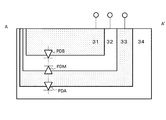
図3は、光電変換部211に含まれるフォトダイオードの平面図である。34は第2導電型の半導体基板である。31は、第1導電型の半導体領域で形成された第1の光電変換部である。2は、第2導電型の半導体領域で形成された第2の光電変換部である。33は、第1導電型の半導体領域で形成された第3の光電変換部である。第2導電型半導体領域32の面積は、第1導電型半導体領域31の面積以上である。光電変換装置は、半導体基板34に形成される。
FIG. 3 is a plan view of a photodiode included in the
図4は、図3のフォトダイオードをA−A'で切った際の断面図である。第2導電型半導体領域32は、半導体基板の深さ方向に対して、第1導電型半導体領域31より深い位置に形成される。第1導電型半導体領域33は、半導体基板の深さ方向に対して、第2導電型半導体領域32より深い位置に形成される。第1導電型半導体領域31と第2導電型半導体領域32によって形成されるフォトダイオードをPDBとする。同様に、第2導電型半導体領域32と第1導電型半導体領域33によって形成されるフォトダイオードをPDM、第1導電型半導体領域33と第2導電型半導体領域34によって形成されるフォトダイオードをPDAとする。この構成により、第1導電型半導体領域31に照射される被写体の位置情報の光と対応する位置の光を、半導体領域32及び33でも受ける事が可能となる。以降では、第1導電型半導体領域をp型とし、第2導電型半導体領域をn型として説明するが、原理的には導電型にはよらないので、第1導電型半導体領域をn型とし、第2導電型半導体領域をp型としても効果が変わるものではない。また、以降では、半導体領域31、32、33の3層構造として説明するが、これに限定されない。第1導電型半導体領域33より深い位置にさらに第2導電型半導体領域を形成し、その第2導電型半導体領域よりも深い位置にさらに第1導電型半導体領域を形成してもよい。これにより、フォトダイオードPDAより深い位置に第4の光電変換部及び第5の光電変換部を形成する等、3層以上の構成にすることができる。逆に、フォトダイオードPDMと、フォトダイオードPDA又はPDBからなる2層の構造としても良い。
4 is a cross-sectional view of the photodiode of FIG. 3 taken along AA ′. The second conductivity
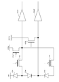
図5は、単位画素21の等価回路図であり、図2及び図4と同じ構成部材には同じ符号を付している。フォトダイオードPDA、PDB及びPDMは、光を電荷に変換する。図4において、第1導電型半導体領域31は、フォトダイオードPDBの出力ノードである。第2導電型半導体領域32は、フォトダイオードPDMの出力ノードである。第1導電型半導体領域33は、フォトダイオードPDAの出力ノードである。トランジスタTXA及びTXBは、それぞれ、フォトダイオードPDA及びPDBに蓄積された電荷を転送する為の転送トランジスタである。トランジスタRESA,RESM及びRESBは、それぞれ、フォトダイオードPDA、PDM及びPDBを初期状態にリセットする為のリセットトランジスタである。電圧VRESA、VRESM及びVRESBは、それぞれ、フォトダイオードPDA、PDM及びPDBのリセット電源電圧である。フォトダイオードPDA及びPDBは、位置情報を検出する為のフォトダイオードである。フォトダイオードPDMは、フォトダイオードPDA及びPDBの電荷蓄積量を推測する為のモニタ用のフォトダイオードである。フォトダイオードPDAのアノードは、転送トランジスタTXAを介してアンプAmpAの入力ノードに接続される。フォトダイオードPDMのカソードは、転送トランジスタを介さず直接アンプAmpMの入力ノードに接続される。これにより、アンプAmpMの出力ノードからは、フォトダイオードPDMに蓄積した電荷量に応じた信号が常に出力され、モニタ部23は、光電変換部211で受けている光量をリアルタイムにモニタリングする事が可能である。フォトダイオードPDBは、フォトダイオードPDAと同様に、転送トランジスタTXBを介してアンプAmpBの入力ノードに接続される。モニタ部23は、フォトダイオードPDA及びPDBの電荷蓄積期間中に、フォトダイオードPDMの信号をモニタリングする。転送トランジスタTXA及びTXBをオフすることにより、フォトダイオードPDA及びPDBは電荷を蓄積することができる。
FIG. 5 is an equivalent circuit diagram of the
フォトダイオードPDA及びPDBは、それぞれ、転送トランジスタTXA及びTXBを介してアンプAmpA及びAmpBに接続されているため、高S/Nであるが、転送動作を行わないと蓄積された電荷量を検出することができない。そこで、フォトダイオードPDA及びPDBに蓄積された電荷量を推測する為のモニタフォトダイオードPDMが必要となる。特許文献1の図5に示される構成では、被写体の位置情報の光を検出する為のフォトダイオードとモニタフォトダイオードの位置が平面で異なる為、フォトダイオードに入射する光をモニタフォトダイオードで受ける事はできない。特許文献1と比べ、本実施形態の優れている点は、図4から明らかなようにフォトダイオードPDA及びPDBに入射する光に対応する位置の光をモニタフォトダイオードPDMで受ける事が可能な点である。 The photodiodes PDA and PDB are connected to the amplifiers AmpA and AmpB via the transfer transistors TXA and TXB, respectively. Therefore, the photodiodes PDA and PDB have high S / N, but detect the accumulated charge amount when the transfer operation is not performed. I can't. Therefore, a monitor photodiode PDM is required for estimating the amount of charge accumulated in the photodiodes PDA and PDB. In the configuration shown in FIG. 5 of Patent Document 1, since the position of the photodiode for detecting the light of the position information of the subject and the position of the monitor photodiode are different on a plane, the light incident on the photodiode is received by the monitor photodiode. I can't. Compared with Patent Document 1, this embodiment is superior in that the monitor photodiode PDM can receive light at a position corresponding to light incident on the photodiodes PDA and PDB, as is apparent from FIG. It is.
以上の様に、本実施形によれば、モニタ部23は、フォトダイオードPDA及びPDBと同じ光を受けているフォトダイオードPDMの出力信号を常時モニタリングする。これにより、転送動作を行わずにフォトダイオードPDA及びPDBに蓄積された電荷量を精度よく推測する事が可能となる。
As described above, according to the present embodiment, the
(第2の実施形態)
図6は、本発明の第2の実施形態に係る基準部用ラインセンサ12及び参照用ラインセンサ13の構成例を示す図である。図2と同じ構成には、同じ符号を付している。本実施形態と第1の実施形態との相違点は、信号保持部22とバッファBufAの間に切り替え手段(切り替え部)61を接続し、バッファを1個のバッファBufAにしている点である。切り替え手段61は、モニタ部23から出力される信号により制御される。フォトダイオードPDAの感度よりもフォトダイオードPDBの感度の方が大きいとする。この環境下では、切り替え手段61は、明るい環境では、感度の低いフォトダイオードPDAが接続されるノードとバッファBufAを接続する。また、暗い環境下では、切り替え手段61は、感度の高いフォトダイオードPDBが接続されるノードとバッファBufAを接続する。以上の様に、本実施形態によれば、切り替え手段61は、フォトダイオードPDA及びPDBのいずれか1つの信号を出力する事によって、1つのバッファBufAで感度切り替えの機能が実現可能である。
(Second Embodiment)
FIG. 6 is a diagram illustrating a configuration example of the
(第3の実施形態)
図7は、本発明の第3の実施形態に係る基準部用ラインセンサ12及び参照用ラインセンサ13の構成例を示す図である。図2と同じ構成には、同じ符号を付している。本実施形態と第1の実施形態との相違点は、図2のアンプAmpB及びバッファBufBが取り除かれた点である。
(Third embodiment)
FIG. 7 is a diagram illustrating a configuration example of the
図8は、本実施形態の単位画素21の構成例を示す図である。図5と同じ構成には同じ符号を付している。本実施形態と第1の実施形態との相違点は、アンプAmpBが取り除かれ、フォトダイオードPDBは、転送トランジスタTXBを介してアンプAmpAの入力ノードに接続されている点である。転送トランジスタTXA及びTXBは、モニタ部23から出力される信号によって制御される。この構成により、転送トランジスタTXA及びTXBは、同じノードに接続されている為、フォトダイオードPDAで発生した電荷(信号)とフォトダイオードPDBで発生した電荷(信号)を加算する事ができる加算部として機能する。
FIG. 8 is a diagram illustrating a configuration example of the
本実施形態によれば、深い位置に形成されている長波長の光感度が高いフォトダイオードPDAの出力と、浅い位置に形成されている短波長の光感度が高いフォトダイオードPDBの出力を加算する事ができる。これにより、位置情報を検出する為のフォトダイオードPDA,PDBと、そのフォトダイオードPDA,PDBの電荷蓄積量を推測する為のフォトダイオードPDM間の分光特性の差を小さくする事が可能である。また、低感度時には、フォトダイオードPDA又はPDBのみの出力を用い、高感度時には両フォトダイオードPDA及びPDBの電荷を加算した出力を用いるという感度切り替えの機能としても利用可能である。 According to the present embodiment, the output of the photodiode PDA having high photosensitivity of long wavelength formed at a deep position and the output of the photodiode PDB having high photosensitivity of short wavelength formed at a shallow position are added. I can do things. This makes it possible to reduce the difference in spectral characteristics between the photodiodes PDA and PDB for detecting position information and the photodiode PDM for estimating the charge accumulation amount of the photodiodes PDA and PDB. Further, it can also be used as a sensitivity switching function in which the output of only the photodiode PDA or PDB is used when the sensitivity is low, and the output obtained by adding the charges of the photodiodes PDA and PDB is used when the sensitivity is high.
(第4の実施形態)
図9は、本発明の第4の実施形態に係る基準部用ラインセンサ12及び参照用ラインセンサ13の構成例を示す図である。図2と同じ構成には、同じ符号を付している。本実施形態と第1の実施形態との相違点は、モニタ部23の中にアンプ制御部91を備えている点である。アンプ制御部91は、差分信号P−Bの振幅が小さいと判断した場合、振幅を十分大きくするのに必要な増幅率を求め、不図示のアンプによって前述の増幅率で、バッファBufA及びBufBの入力信号を増幅させる。バッファBufA及びBufBには、増幅後の信号が入力される。本実施形態によれば、アンプ制御部91は、フォトダイオードPDMの出力信号に基づき、フォトダイオードPDA及びPDBの出力信号の増幅率を制御する。これにより、差分信号P−Bの振幅が小さい場合でも、適切な増幅率により信号を増幅し、十分大きな信号振幅を得る事が可能になる。
(Fourth embodiment)
FIG. 9 is a diagram illustrating a configuration example of the
(第5の実施形態)
図10は、本発明の第5の実施形態に係る基準部用ラインセンサ12及び参照用ラインセンサ13の構成例を示す図である。図2と同じ構成には、同じ符号を付している。本実施形態と第1の実施形態との相違点は、モニタ部23と単位画素21との間に蓄積時間制御部101を備えている点である。以下、基準部用ラインセンサ12及び参照用ラインセンサ13の駆動方法を説明する。モニタ部23は、差分信号P−Bの振幅が予め定められた閾値を超えたと判断されると、蓄積時間制御部101へ蓄積終了を指示する信号を出力する。信号を受信した蓄積時間制御部101は、各単位画素21に含まれる転送トランジスタTXA及びTXBを制御し、フォトダイオードPDA及びPDBに蓄積された電荷を読み出す。本実施形態によれば、蓄積時間制御部101は、フォトダイオードPDMの出力信号に基づき、フォトダイオードPDA及びPDBの電荷蓄積時間を制御する事により、所望の大きさの信号振幅を得る事が可能となる。すなわち、複数のフォトダイオードPDM,PDA,PDBのうちの一方のフォトダイオードPDMに基づく信号に応じて、他方のフォトダイオードPDA,PDBの電荷蓄積時間を制御する。
(Fifth embodiment)
FIG. 10 is a diagram illustrating a configuration example of the reference
(第6の実施形態)
図11は、本発明の第6の実施形態に係る単位画素21の構成例を示す図である。図5と同じ構成には、同じ符号を付している。本実施形態と第1の実施形態との相違点は、アンプAmpMが電流積分型アンプで構成されている点であり、キャパシタC、アンプAmp及び基準電源Vrefを有する。キャパシタCは、光電流を積分する為のキャパシタである。アンプAmpは、差動アンプである。Vrefは基準電源である。この構成により、アンプAmpMは、光電流を積分した値に基づいた信号を出力する。また、仮想接地によって、第2導電型半導体領域32を一定の電位Vrefに保つ事が可能となる。第2導電型半導体領域32を一定電位とする事により、半導体中のエネルギーポテンシャルが変動する事による空乏層幅の変化を抑制可能となる。フォトダイオードは深さによって波長ごとの光感度が違う為、空乏層幅が深さ方向で変化すると分光特性が変化してしまう。本実施形によれば、アンプAmpMは、第2導電型半導体領域32の電位を固定し、フォトダイオードPDMから出力される電流を時間積分した信号を出力する。これにより、空乏層幅の変化を抑制し、フォトダイオードPDAとフォトダイオードPDBの分光特性の変化を抑制する事が可能となる。
(Sixth embodiment)
FIG. 11 is a diagram illustrating a configuration example of the
以上のように、第1〜第6の実施形態によれば、被写体の位置情報を検出するための光電変換部31,33とモニタ用光電変換部32の位置が平面上でほぼ一致する。そのため、被写体の位置情報を検出するための光電変換部31,33に照射されている光を高精度でモニタする事が可能である。したがって、これら光電変換部31〜33から得られる信号の受光位置相関性を向上出来るので、光電変換部31〜33の出力レベル差を低減でき、電荷蓄積時間の制御性能を向上させることができる。
As described above, according to the first to sixth embodiments, the positions of the
(第7の実施形態)
図12は、本発明の第7の実施形態に係る撮像システムの構成例を示すブロック図である。901は後述するレンズのプロテクトを行うバリア、902は被写体の光学像を固体撮像装置904に結像するレンズ、903はレンズを通過した光量を調整するための絞りである。904はレンズで結像された被写体の光学像を画像信号として取得する固体撮像装置である。905は先述の各実施形態で説明した光電変換装置を用いたAFセンサ(焦点検出装置)である。
(Seventh embodiment)
FIG. 12 is a block diagram illustrating a configuration example of an imaging system according to the seventh embodiment of the present invention.
906は固体撮像装置904やAFセンサ905から出力される信号を処理するアナログ信号処理装置、907は信号処理装置906から出力された信号をアナログデジタル変換するA/D変換器である。908はA/D変換器907より出力された画像データに対して各種の補正や、データを圧縮するデジタル信号処理部である。
909は画像データを一時記憶するためのメモリ部、910は外部コンピュータなどと通信するための外部I/F回路、911はデジタル信号処理部908などに各種タイミング信号を出力するタイミング発生部である。912は各種演算とカメラ全体を制御する全体制御・演算部、913は記録媒体制御I/F部、914は取得した画像データを記録、又は読み出しを行うための半導体メモリなどの着脱可能な記録媒体、915は外部コンピュータである。
次に、上記の撮像システムの撮影時の動作について説明する。バリア901がオープンされ、AFセンサ905から出力された信号をもとに、全体制御・演算部912は前記したような位相差検出により被写体までの距離を演算する。その後、演算結果に基づいてレンズ902を駆動し、再び合焦しているか否かを判断し、合焦していないと判断したときには、再びレンズ902を駆動するオートフォーカス制御を行う。次いで、合焦が確認された後に固体撮像装置904による電荷蓄積動作が始まる。固体撮像装置904の電荷蓄積動作が終了すると、固体撮像装置904から出力された画像信号はA/D変換器907でアナログデジタル変換され、デジタル信号処理部908を通り全体制御・演算部912によりメモリ部909に書き込まれる。その後、メモリ部909に蓄積されたデータは全体制御・演算部912の制御により記録媒体制御I/F部910を介して記録媒体914に記録される。また、外部I/F部910を通り直接コンピュータ915などに入力してもよい。
Next, the operation at the time of shooting of the above imaging system will be described. Based on the signal output from the
なお、上記実施形態は、何れも本発明を実施するにあたっての具体化の例を示したものに過ぎず、これらによって本発明の技術的範囲が限定的に解釈されてはならないものである。すなわち、本発明はその技術思想、又はその主要な特徴から逸脱することなく、様々な形で実施することができる。 The above-described embodiments are merely examples of implementation in carrying out the present invention, and the technical scope of the present invention should not be construed in a limited manner. That is, the present invention can be implemented in various forms without departing from the technical idea or the main features thereof.
31 第1の光電変換部、32 第2の光電変換部、33 第3の光電変換部、23 モニタ部 31 1st photoelectric conversion part, 32 2nd photoelectric conversion part, 33 3rd photoelectric conversion part, 23 monitor part
Claims (13)
第1導電型で形成された第1の光電変換部と、
前記半導体基板の深さ方向に対して前記第1の光電変換部より深い位置に形成され、第2導電型で形成された第2の光電変換部と、
前記半導体基板の深さ方向に対して前記第2の光電変換部より深い位置に形成され、第1導電型で形成された第3の光電変換部と、
前記第1の光電変換部及び前記第3の光電変換部の電荷蓄積期間中に、前記第2の光電変換部の信号をモニタリングするモニタ部とを有し、
前記第1の光電変換部、前記第2の光電変換部、及び前記第3の光電変換部は、平面視において重なることを特徴とする光電変換装置。 A photoelectric conversion device formed on a semiconductor substrate,
A first photoelectric conversion unit formed of a first conductivity type;
A second photoelectric conversion unit formed at a position deeper than the first photoelectric conversion unit with respect to the depth direction of the semiconductor substrate and formed of a second conductivity type;
A third photoelectric conversion unit formed at a position deeper than the second photoelectric conversion unit with respect to the depth direction of the semiconductor substrate and formed of a first conductivity type;
During the first photoelectric conversion unit and the third charge accumulation period of the photoelectric conversion unit, have a monitor unit for monitoring a signal of the second photoelectric conversion unit,
The first photoelectric conversion unit, the second photoelectric conversion unit, and the third photoelectric conversion unit overlap in a plan view .
光学像を結像するレンズとを有し、
前記レンズは、前記焦点検出装置の出力信号に応じて駆動されることを特徴とする撮像システム。 A focus detection apparatus according to claim 9 ;
A lens for forming an optical image,
The imaging system, wherein the lens is driven in accordance with an output signal of the focus detection device.
前記半導体基板の深さ方向に対して前記第1の光電変換部より深い位置に形成されて前記第1の光電変換部と平面視において重なり、第2導電型で形成された第2の光電変換部とを有する光電変換装置の駆動方法であって、
前記第1の光電変換部及び前記第2の光電変換部のうちの一方に基づく信号に応じて、他方の電荷蓄積時間を制御することを特徴とする光電変換装置の駆動方法。 A first photoelectric conversion unit formed of a first conductivity type of a semiconductor substrate;
A second photoelectric conversion formed in a second conductivity type, which is formed at a position deeper than the first photoelectric conversion unit with respect to the depth direction of the semiconductor substrate and overlaps the first photoelectric conversion unit in plan view ; A method of driving a photoelectric conversion device having a portion,
A method for driving a photoelectric conversion device, comprising: controlling a charge accumulation time of the other in accordance with a signal based on one of the first photoelectric conversion unit and the second photoelectric conversion unit.
Priority Applications (2)
| Application Number | Priority Date | Filing Date | Title |
|---|---|---|---|
| JP2013167683A JP6223055B2 (en) | 2013-08-12 | 2013-08-12 | Photoelectric conversion device |
| US14/325,874 US9357122B2 (en) | 2013-08-12 | 2014-07-08 | Photoelectric conversion apparatus, focus detecting apparatus, imaging system, and driving method of photoelectric conversion apparatus |
Applications Claiming Priority (1)
| Application Number | Priority Date | Filing Date | Title |
|---|---|---|---|
| JP2013167683A JP6223055B2 (en) | 2013-08-12 | 2013-08-12 | Photoelectric conversion device |
Publications (3)
| Publication Number | Publication Date |
|---|---|
| JP2015037217A JP2015037217A (en) | 2015-02-23 |
| JP2015037217A5 JP2015037217A5 (en) | 2016-07-28 |
| JP6223055B2 true JP6223055B2 (en) | 2017-11-01 |
Family
ID=52448339
Family Applications (1)
| Application Number | Title | Priority Date | Filing Date |
|---|---|---|---|
| JP2013167683A Expired - Fee Related JP6223055B2 (en) | 2013-08-12 | 2013-08-12 | Photoelectric conversion device |
Country Status (2)
| Country | Link |
|---|---|
| US (1) | US9357122B2 (en) |
| JP (1) | JP6223055B2 (en) |
Families Citing this family (26)
| Publication number | Priority date | Publication date | Assignee | Title |
|---|---|---|---|---|
| JP6245997B2 (en) | 2014-01-16 | 2017-12-13 | キヤノン株式会社 | Solid-state imaging device and imaging system |
| JP6246004B2 (en) | 2014-01-30 | 2017-12-13 | キヤノン株式会社 | Solid-state imaging device |
| JP6057931B2 (en) | 2014-02-10 | 2017-01-11 | キヤノン株式会社 | Photoelectric conversion device and imaging system using the same |
| JP6412328B2 (en) | 2014-04-01 | 2018-10-24 | キヤノン株式会社 | Solid-state imaging device and camera |
| JP6457822B2 (en) | 2015-01-21 | 2019-01-23 | キヤノン株式会社 | Photoelectric conversion device and imaging system |
| JP6619631B2 (en) | 2015-11-30 | 2019-12-11 | キヤノン株式会社 | Solid-state imaging device and imaging system |
| JP6889571B2 (en) | 2017-02-24 | 2021-06-18 | キヤノン株式会社 | Imaging device and imaging system |
| JP6946046B2 (en) | 2017-04-28 | 2021-10-06 | キヤノン株式会社 | Photoelectric conversion device and its driving method |
| JP7146424B2 (en) | 2018-03-19 | 2022-10-04 | キヤノン株式会社 | Photoelectric conversion device and imaging system |
| JP7171213B2 (en) | 2018-04-02 | 2022-11-15 | キヤノン株式会社 | Photoelectric conversion device and imaging system |
| US11463644B2 (en) | 2018-08-31 | 2022-10-04 | Canon Kabushiki Kaisha | Imaging device, imaging system, and drive method of imaging device |
| JP7152912B2 (en) | 2018-09-06 | 2022-10-13 | キヤノン株式会社 | Photoelectric conversion device and imaging system |
| JP6852041B2 (en) | 2018-11-21 | 2021-03-31 | キヤノン株式会社 | Photoelectric conversion device and imaging system |
| JP6986046B2 (en) | 2019-05-30 | 2021-12-22 | キヤノン株式会社 | Photoelectric converters and equipment |
| JP7345301B2 (en) | 2019-07-18 | 2023-09-15 | キヤノン株式会社 | Photoelectric conversion devices and equipment |
| JP7374639B2 (en) | 2019-07-19 | 2023-11-07 | キヤノン株式会社 | Photoelectric conversion device and imaging system |
| JP7303682B2 (en) | 2019-07-19 | 2023-07-05 | キヤノン株式会社 | Photoelectric conversion device and imaging system |
| JP7171649B2 (en) | 2020-05-15 | 2022-11-15 | キヤノン株式会社 | Imaging device and imaging system |
| US11470275B2 (en) | 2020-06-15 | 2022-10-11 | Canon Kabushiki Kaisha | Photoelectric conversion device, photoelectric conversion system and moving body |
| JP2022015925A (en) | 2020-07-10 | 2022-01-21 | キヤノン株式会社 | Photoelectric conversion device and method of driving the same |
| US11736813B2 (en) | 2020-07-27 | 2023-08-22 | Canon Kabushiki Kaisha | Imaging device and equipment |
| JP2022119633A (en) | 2021-02-04 | 2022-08-17 | キヤノン株式会社 | Photoelectric conversion device, electronic device, and substrate |
| JP2022130037A (en) | 2021-02-25 | 2022-09-06 | キヤノン株式会社 | Photoelectric conversion device and apparatus |
| JP2022144242A (en) | 2021-03-18 | 2022-10-03 | キヤノン株式会社 | Photoelectric conversion device, photoelectric conversion system, and movable body |
| JP2022144241A (en) | 2021-03-18 | 2022-10-03 | キヤノン株式会社 | Photoelectric conversion device, substrate, and apparatus |
| JP2022158042A (en) | 2021-04-01 | 2022-10-14 | キヤノン株式会社 | Photoelectric conversion device |
Family Cites Families (24)
| Publication number | Priority date | Publication date | Assignee | Title |
|---|---|---|---|---|
| JP3260820B2 (en) * | 1992-06-08 | 2002-02-25 | オリンパス光学工業株式会社 | Focus detection device |
| JP2004309701A (en) | 2003-04-04 | 2004-11-04 | Olympus Corp | Range-finding/photometric sensor and camera |
| JP4286101B2 (en) * | 2003-10-08 | 2009-06-24 | オリンパス株式会社 | Offset suppression circuit for photodetector |
| JP2005156900A (en) * | 2003-11-26 | 2005-06-16 | Kyocera Corp | Sensor for detecting focal point, focal point detector having the sensor for detecting focal point, focal point detection method and electronic imaging device |
| JP4612869B2 (en) * | 2005-06-08 | 2011-01-12 | キヤノン株式会社 | Focus detection device, imaging device, and focusing method |
| JP5132102B2 (en) | 2006-08-01 | 2013-01-30 | キヤノン株式会社 | Photoelectric conversion device and imaging system using photoelectric conversion device |
| JP4350768B2 (en) | 2007-04-16 | 2009-10-21 | キヤノン株式会社 | Photoelectric conversion device and imaging device |
| JP5063223B2 (en) | 2007-07-02 | 2012-10-31 | キヤノン株式会社 | Photoelectric conversion device and imaging system |
| JP4986761B2 (en) * | 2007-08-03 | 2012-07-25 | キヤノン株式会社 | Imaging device |
| JP5004775B2 (en) | 2007-12-04 | 2012-08-22 | キヤノン株式会社 | Imaging apparatus and imaging system |
| JP5038188B2 (en) | 2008-02-28 | 2012-10-03 | キヤノン株式会社 | Imaging apparatus and imaging system using the same |
| JP5221982B2 (en) | 2008-02-29 | 2013-06-26 | キヤノン株式会社 | Solid-state imaging device and camera |
| JP2010102090A (en) * | 2008-10-23 | 2010-05-06 | Olympus Corp | Signal generator, focusing point detector, and image pickup apparatus |
| JP5241454B2 (en) | 2008-12-01 | 2013-07-17 | キヤノン株式会社 | Solid-state imaging device and imaging system using the same |
| JP5284132B2 (en) | 2009-02-06 | 2013-09-11 | キヤノン株式会社 | Solid-state imaging device, imaging system, and driving method of imaging device |
| JP5614993B2 (en) | 2010-01-19 | 2014-10-29 | キヤノン株式会社 | Imaging apparatus and solid-state imaging device driving method |
| JP2011238856A (en) | 2010-05-12 | 2011-11-24 | Canon Inc | Photoelectric conversion device |
| JP5729947B2 (en) * | 2010-08-27 | 2015-06-03 | キヤノン株式会社 | Photoelectric conversion device, focus detection device, and imaging system |
| JP6045136B2 (en) | 2011-01-31 | 2016-12-14 | キヤノン株式会社 | Photoelectric conversion device |
| JP5917055B2 (en) | 2011-09-13 | 2016-05-11 | キヤノン株式会社 | Solid-state imaging device, driving method thereof, and control program |
| JP2013093553A (en) | 2011-10-04 | 2013-05-16 | Canon Inc | Photoelectric conversion device and manufacturing method therefor, and photoelectric conversion system |
| JP6080447B2 (en) | 2011-12-01 | 2017-02-15 | キヤノン株式会社 | Photoelectric conversion device |
| JP6188281B2 (en) | 2012-05-24 | 2017-08-30 | キヤノン株式会社 | Photoelectric conversion device |
| US8939548B2 (en) | 2013-03-09 | 2015-01-27 | Xerox Corporation | Lamination processes |
-
2013
- 2013-08-12 JP JP2013167683A patent/JP6223055B2/en not_active Expired - Fee Related
-
2014
- 2014-07-08 US US14/325,874 patent/US9357122B2/en not_active Expired - Fee Related
Also Published As
| Publication number | Publication date |
|---|---|
| JP2015037217A (en) | 2015-02-23 |
| US20150042857A1 (en) | 2015-02-12 |
| US9357122B2 (en) | 2016-05-31 |
Similar Documents
| Publication | Publication Date | Title |
|---|---|---|
| JP6223055B2 (en) | Photoelectric conversion device | |
| US10321087B2 (en) | Solid-state image sensor and image sensing system | |
| JP5959829B2 (en) | Solid-state imaging device | |
| JP6555890B2 (en) | Imaging apparatus, imaging system, and driving method of imaging apparatus | |
| JP2008042679A (en) | Photoelectric conversion device and imaging apparatus | |
| US8698930B2 (en) | Photoelectric conversion apparatus, focus detection apparatus, and image pickup system | |
| US8836837B2 (en) | Photoelectric conversion apparatus, focus detecting apparatus, and imaging system | |
| US20120050597A1 (en) | Photoelectric conversion apparatus, focus detection apparatus, and image pickup system | |
| JP5729947B2 (en) | Photoelectric conversion device, focus detection device, and imaging system | |
| JP2022002355A (en) | Solid state image sensor, control method for solid state image sensor and electronic apparatus | |
| US9258505B2 (en) | Imaging apparatus, imaging system, method for driving imaging apparatus, and method for driving imaging system | |
| JP2019068382A (en) | Solid state image sensor and imaging system | |
| US10116854B2 (en) | Photoelectric conversion apparatus, switching an electric path between a conductive state and a non-conductive state | |
| US20130063632A1 (en) | Focus detecting apparatus and driving method therefor | |
| US8786723B2 (en) | Photoelectric-conversion device | |
| US9813646B2 (en) | Solid-state imaging apparatus, imaging system, and method for driving solid-state imaging apparatus, where longer accumulation time is used for light-shielded pixels | |
| JP2013171178A (en) | Autofocus device, autofocus control method, and imaging apparatus | |
| US9080914B2 (en) | Photoelectric conversion apparatus using fixed pattern noises of sensor and memory cells | |
| JP5460465B2 (en) | Photoelectric conversion device and imaging system | |
| JP5142680B2 (en) | Photoelectric conversion device and imaging system | |
| WO2018124056A1 (en) | Imaging device and control method therefor | |
| KR20150130186A (en) | Image sensor and stacked structure thereof | |
| US9264640B2 (en) | Photoelectric conversion apparatus, method for driving photoelectric conversion apparatus, and imaging system | |
| JP4928102B2 (en) | Solid-state imaging device for focus detection, and camera using the solid-state imaging device | |
| JP2015149672A (en) | Photoelectric converter and photoelectric conversion system |
Legal Events
| Date | Code | Title | Description |
|---|---|---|---|
| A521 | Request for written amendment filed |
Free format text: JAPANESE INTERMEDIATE CODE: A523 Effective date: 20160606 |
|
| A621 | Written request for application examination |
Free format text: JAPANESE INTERMEDIATE CODE: A621 Effective date: 20160606 |
|
| A977 | Report on retrieval |
Free format text: JAPANESE INTERMEDIATE CODE: A971007 Effective date: 20170213 |
|
| A131 | Notification of reasons for refusal |
Free format text: JAPANESE INTERMEDIATE CODE: A131 Effective date: 20170221 |
|
| A521 | Request for written amendment filed |
Free format text: JAPANESE INTERMEDIATE CODE: A523 Effective date: 20170419 |
|
| TRDD | Decision of grant or rejection written | ||
| A01 | Written decision to grant a patent or to grant a registration (utility model) |
Free format text: JAPANESE INTERMEDIATE CODE: A01 Effective date: 20170905 |
|
| A61 | First payment of annual fees (during grant procedure) |
Free format text: JAPANESE INTERMEDIATE CODE: A61 Effective date: 20171003 |
|
| R151 | Written notification of patent or utility model registration |
Ref document number: 6223055 Country of ref document: JP Free format text: JAPANESE INTERMEDIATE CODE: R151 |
|
| LAPS | Cancellation because of no payment of annual fees |