JP6080447B2 - Photoelectric conversion device - Google Patents
Photoelectric conversion device Download PDFInfo
- Publication number
- JP6080447B2 JP6080447B2 JP2012203185A JP2012203185A JP6080447B2 JP 6080447 B2 JP6080447 B2 JP 6080447B2 JP 2012203185 A JP2012203185 A JP 2012203185A JP 2012203185 A JP2012203185 A JP 2012203185A JP 6080447 B2 JP6080447 B2 JP 6080447B2
- Authority
- JP
- Japan
- Prior art keywords
- current
- photoelectric conversion
- terminal
- conversion element
- field effect
- Prior art date
- Legal status (The legal status is an assumption and is not a legal conclusion. Google has not performed a legal analysis and makes no representation as to the accuracy of the status listed.)
- Expired - Fee Related
Links
- 238000006243 chemical reaction Methods 0.000 title claims description 196
- 238000001514 detection method Methods 0.000 claims description 53
- 230000005669 field effect Effects 0.000 claims description 33
- 239000000872 buffer Substances 0.000 claims description 8
- 230000035945 sensitivity Effects 0.000 claims description 7
- 238000010030 laminating Methods 0.000 claims 1
- 230000007423 decrease Effects 0.000 description 12
- 230000003287 optical effect Effects 0.000 description 10
- 230000000694 effects Effects 0.000 description 8
- 230000004044 response Effects 0.000 description 7
- 230000003321 amplification Effects 0.000 description 5
- 238000003199 nucleic acid amplification method Methods 0.000 description 5
- 230000003111 delayed effect Effects 0.000 description 4
- 238000010586 diagram Methods 0.000 description 4
- 230000003595 spectral effect Effects 0.000 description 4
- 239000003990 capacitor Substances 0.000 description 3
- 238000005513 bias potential Methods 0.000 description 2
- 230000005684 electric field Effects 0.000 description 2
- 239000010410 layer Substances 0.000 description 2
- 238000000034 method Methods 0.000 description 2
- XUIMIQQOPSSXEZ-UHFFFAOYSA-N Silicon Chemical compound [Si] XUIMIQQOPSSXEZ-UHFFFAOYSA-N 0.000 description 1
- 230000006866 deterioration Effects 0.000 description 1
- 239000012535 impurity Substances 0.000 description 1
- 239000011229 interlayer Substances 0.000 description 1
- 230000001678 irradiating effect Effects 0.000 description 1
- 230000003071 parasitic effect Effects 0.000 description 1
- 230000004043 responsiveness Effects 0.000 description 1
- 239000004065 semiconductor Substances 0.000 description 1
- 229910052710 silicon Inorganic materials 0.000 description 1
- 239000010703 silicon Substances 0.000 description 1
- 238000004088 simulation Methods 0.000 description 1
Images


Classifications
-
- H—ELECTRICITY
- H01—ELECTRIC ELEMENTS
- H01L—SEMICONDUCTOR DEVICES NOT COVERED BY CLASS H10
- H01L31/00—Semiconductor devices sensitive to infrared radiation, light, electromagnetic radiation of shorter wavelength or corpuscular radiation and specially adapted either for the conversion of the energy of such radiation into electrical energy or for the control of electrical energy by such radiation; Processes or apparatus specially adapted for the manufacture or treatment thereof or of parts thereof; Details thereof
- H01L31/02—Details
- H01L31/02016—Circuit arrangements of general character for the devices
- H01L31/02019—Circuit arrangements of general character for the devices for devices characterised by at least one potential jump barrier or surface barrier
-
- H—ELECTRICITY
- H01—ELECTRIC ELEMENTS
- H01L—SEMICONDUCTOR DEVICES NOT COVERED BY CLASS H10
- H01L31/00—Semiconductor devices sensitive to infrared radiation, light, electromagnetic radiation of shorter wavelength or corpuscular radiation and specially adapted either for the conversion of the energy of such radiation into electrical energy or for the control of electrical energy by such radiation; Processes or apparatus specially adapted for the manufacture or treatment thereof or of parts thereof; Details thereof
- H01L31/02—Details
- H01L31/02002—Arrangements for conducting electric current to or from the device in operations
-
- H—ELECTRICITY
- H01—ELECTRIC ELEMENTS
- H01L—SEMICONDUCTOR DEVICES NOT COVERED BY CLASS H10
- H01L27/00—Devices consisting of a plurality of semiconductor or other solid-state components formed in or on a common substrate
- H01L27/14—Devices consisting of a plurality of semiconductor or other solid-state components formed in or on a common substrate including semiconductor components sensitive to infrared radiation, light, electromagnetic radiation of shorter wavelength or corpuscular radiation and specially adapted either for the conversion of the energy of such radiation into electrical energy or for the control of electrical energy by such radiation
- H01L27/144—Devices controlled by radiation
- H01L27/146—Imager structures
- H01L27/14643—Photodiode arrays; MOS imagers
- H01L27/14649—Infrared imagers
- H01L27/14652—Multispectral infrared imagers, having a stacked pixel-element structure, e.g. npn, npnpn or MQW structures
-
- H—ELECTRICITY
- H01—ELECTRIC ELEMENTS
- H01L—SEMICONDUCTOR DEVICES NOT COVERED BY CLASS H10
- H01L31/00—Semiconductor devices sensitive to infrared radiation, light, electromagnetic radiation of shorter wavelength or corpuscular radiation and specially adapted either for the conversion of the energy of such radiation into electrical energy or for the control of electrical energy by such radiation; Processes or apparatus specially adapted for the manufacture or treatment thereof or of parts thereof; Details thereof
- H01L31/08—Semiconductor devices sensitive to infrared radiation, light, electromagnetic radiation of shorter wavelength or corpuscular radiation and specially adapted either for the conversion of the energy of such radiation into electrical energy or for the control of electrical energy by such radiation; Processes or apparatus specially adapted for the manufacture or treatment thereof or of parts thereof; Details thereof in which radiation controls flow of current through the device, e.g. photoresistors
- H01L31/10—Semiconductor devices sensitive to infrared radiation, light, electromagnetic radiation of shorter wavelength or corpuscular radiation and specially adapted either for the conversion of the energy of such radiation into electrical energy or for the control of electrical energy by such radiation; Processes or apparatus specially adapted for the manufacture or treatment thereof or of parts thereof; Details thereof in which radiation controls flow of current through the device, e.g. photoresistors characterised by at least one potential-jump barrier or surface barrier, e.g. phototransistors
- H01L31/101—Devices sensitive to infrared, visible or ultraviolet radiation
- H01L31/1013—Devices sensitive to infrared, visible or ultraviolet radiation devices sensitive to two or more wavelengths, e.g. multi-spectrum radiation detection devices
-
- H—ELECTRICITY
- H01—ELECTRIC ELEMENTS
- H01L—SEMICONDUCTOR DEVICES NOT COVERED BY CLASS H10
- H01L31/00—Semiconductor devices sensitive to infrared radiation, light, electromagnetic radiation of shorter wavelength or corpuscular radiation and specially adapted either for the conversion of the energy of such radiation into electrical energy or for the control of electrical energy by such radiation; Processes or apparatus specially adapted for the manufacture or treatment thereof or of parts thereof; Details thereof
- H01L31/08—Semiconductor devices sensitive to infrared radiation, light, electromagnetic radiation of shorter wavelength or corpuscular radiation and specially adapted either for the conversion of the energy of such radiation into electrical energy or for the control of electrical energy by such radiation; Processes or apparatus specially adapted for the manufacture or treatment thereof or of parts thereof; Details thereof in which radiation controls flow of current through the device, e.g. photoresistors
- H01L31/10—Semiconductor devices sensitive to infrared radiation, light, electromagnetic radiation of shorter wavelength or corpuscular radiation and specially adapted either for the conversion of the energy of such radiation into electrical energy or for the control of electrical energy by such radiation; Processes or apparatus specially adapted for the manufacture or treatment thereof or of parts thereof; Details thereof in which radiation controls flow of current through the device, e.g. photoresistors characterised by at least one potential-jump barrier or surface barrier, e.g. phototransistors
- H01L31/101—Devices sensitive to infrared, visible or ultraviolet radiation
- H01L31/102—Devices sensitive to infrared, visible or ultraviolet radiation characterised by only one potential barrier or surface barrier
- H01L31/103—Devices sensitive to infrared, visible or ultraviolet radiation characterised by only one potential barrier or surface barrier the potential barrier being of the PN homojunction type
-
- G—PHYSICS
- G01—MEASURING; TESTING
- G01J—MEASUREMENT OF INTENSITY, VELOCITY, SPECTRAL CONTENT, POLARISATION, PHASE OR PULSE CHARACTERISTICS OF INFRARED, VISIBLE OR ULTRAVIOLET LIGHT; COLORIMETRY; RADIATION PYROMETRY
- G01J1/00—Photometry, e.g. photographic exposure meter
- G01J1/42—Photometry, e.g. photographic exposure meter using electric radiation detectors
- G01J1/44—Electric circuits
-
- H—ELECTRICITY
- H01—ELECTRIC ELEMENTS
- H01L—SEMICONDUCTOR DEVICES NOT COVERED BY CLASS H10
- H01L27/00—Devices consisting of a plurality of semiconductor or other solid-state components formed in or on a common substrate
- H01L27/14—Devices consisting of a plurality of semiconductor or other solid-state components formed in or on a common substrate including semiconductor components sensitive to infrared radiation, light, electromagnetic radiation of shorter wavelength or corpuscular radiation and specially adapted either for the conversion of the energy of such radiation into electrical energy or for the control of electrical energy by such radiation
- H01L27/144—Devices controlled by radiation
- H01L27/146—Imager structures
- H01L27/14601—Structural or functional details thereof
- H01L27/1462—Coatings
- H01L27/14623—Optical shielding
Description
本発明は、光電変換装置に関する。 The present invention relates to a photoelectric conversion device.
特許文献1は、フォトトランジスタとフィードバック手段を用いた光電変換装置を開示している。その光電変換装置は、定電流源とその定電流源によって駆動されるMOSFETでソース接地回路を構成しており、そのMOSFETのゲートとソース間の電圧で、フォトトランジスタのベース電位を定めている。また、その光電変換装置は、光量が変化した際、フォトトランジスタのコレクタ電流が変化するので、そのベースとエミッタ間の電圧が変化するが、この時、フォトトランジスタのベース電位ではなくエミッタ電位が主に変動する構成となっている。光電流でバイアスされたベースではなく、より大きな電流(〜hFE×光電流)でバイアスされたエミッタの電位が動くようにすることで光応答性を向上させている。すなわち、光量が変化してから、ベース電位とエミッタ電位の変化が完了するまでの時間の短縮を行っている。
本発明の目的は、光応答特性の良い光電変換装置を提供することである。 An object of the present invention is to provide a photoelectric conversion device with good optical response characteristics.
本発明の光電変換装置は、第1の端子と、第1の電流出力端子と、第1の光電変換素子と、第1の検出手段と、第1のフィードバック手段と、電流供給手段とを有し、前記第1の端子は、前記第1の光電変換素子と、前記第1の検出手段と、前記第1のフィードバック手段と、前記電流供給手段とに接続され、前記第1のフィードバック手段は、さらに前記第1の電流出力端子に接続され、前記第1の光電変換素子は、光電変換により電流を前記第1の端子に出力し、前記第1の検出手段は、前記第1の端子の電位に基づく電位を前記第1のフィードバック手段に出力し、前記第1のフィードバック手段は、前記第1の端子の電位に基づく電位を前記第1の端子にフィードバックし、前記第1の光電変換素子が出力する電流に基づく電流を前記第1の電流出力端子に出力し、前記電流供給手段は、前記第1の端子へ電流を供給する電流源であって、前記電流源が供給する電流と、光を受けた前記第1の光電変換素子が生成する電流とを加算した加算電流が、前記第1の端子に供給され、前記加算電流によって前記第1の光電変換素子の光量が検出されることを特徴とする。 The photoelectric conversion device of the present invention includes a first terminal, a first current output terminal, a first photoelectric conversion element, a first detection unit, a first feedback unit, and a current supply unit. The first terminal is connected to the first photoelectric conversion element, the first detection means, the first feedback means, and the current supply means, and the first feedback means is Further, the first photoelectric conversion element is connected to the first current output terminal, the first photoelectric conversion element outputs a current to the first terminal by photoelectric conversion, and the first detection means is connected to the first terminal. A potential based on a potential is output to the first feedback means, and the first feedback means feeds back a potential based on the potential of the first terminal to the first terminal, and the first photoelectric conversion element The current based on the current output by Output to the first current output terminal, said current supply means is a current source for supplying a current to said first terminal, and a current supplied said current source, said first photoelectric which receives light An addition current obtained by adding the current generated by the conversion element is supplied to the first terminal, and the amount of light of the first photoelectric conversion element is detected by the addition current .
電流供給手段によって電流を第1の端子に供給することにより、光応答特性の良い光電変換装置を提供することができる。 By supplying a current to the first terminal by the current supply means, a photoelectric conversion device with good photoresponse characteristics can be provided.
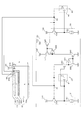
(第1の実施形態)
図2は、本発明の第1の実施形態に係る光電変換装置(センサ)の構成例を示す図である。光電変換装置は、第1の光電変換素子10と、第1の光電変換素子10で発生した光電流が入力される第1の端子20と、第1の検出手段30と、第1のフィードバック手段40と、電流供給手段50と、第1の電流出力端子60とを有する。光電変換素子10は、光電変換により電流を端子20に出力する。検出手段30は、光電変換素子10の端子20の電位を検出する。フィードバック手段40は、検出手段30により検出された電位に基づくフィードバック信号を光電変換素子10の端子20にフィードバックし、光電変換素子10の端子20の電位に基づく電流を電流出力端子60に出力する。電流供給手段50は、光電変換素子10の端子20へ電流を供給する。図2において、光電流が入力される端子20の電位を検出手段30で検出し、フィードバック手段40を用いてフィードバックをかけることによって、光電流が変化した際の端子20の電位変動を低減することができる。
(First embodiment)
FIG. 2 is a diagram illustrating a configuration example of the photoelectric conversion device (sensor) according to the first embodiment of the present invention. The photoelectric conversion device includes a first
本実施形態においては、電流供給手段50から端子20に電流を供給することにより、光応答性を改善することができる。
In the present embodiment, the optical response can be improved by supplying a current from the current supply means 50 to the
図3は、図2の光電変換装置の具体的な回路構成例を示す図である。まず、図2と図3の対応について説明する。第1の光電変換素子10は光電変換を行う第1のフォトダイオードであり、第1の光電変換素子10の第1の端子20は第1のフォトダイオード10のアノードである。第1の検出手段30は、第1の電界効果トランジスタ(MOSFET)100及び第1の電流源(定電流源)90を有する。第1のフィードバック手段40は、第1のバイポーラトランジスタ80及び第2の電界効果トランジスタ(MOSFET)70を有する。フォトダイオード10のアノード20は、第1の電界効果トランジスタ100のゲート及びバイポーラトランジスタ80のベースに接続される。フォトダイオード10のカソードは、電源電圧端子120に接続される。第1の電界効果トランジスタ100は、ソースが電源電圧端子120に接続され、ドレインが第1の電流源90を介してグランド端子に接続される。第2の電界効果トランジスタ70は、ソースがバイポーラトランジスタ80のエミッタに接続され、ゲートが第1の電界効果トランジスタ100のドレインに接続され、ドレインが電流出力端子60に接続される。バイポーラトランジスタ80は、コレクタが電源電圧端子120に接続される。電流供給手段50は、第2の電流源110を有し、電源電圧端子120及びフォトダイオード10のアノード20間に接続される。検出手段30は、定電流源90とMOSFET100のソース接地回路で構成されている。電源電圧端子120は電源Vccに接続されている。本実施形態においては、端子20での光電流が一定値以下となる場合に、電流源110から端子20に一定電流を供給することにより、端子20の電流を一定に保つことができるので、端子20の電位変動を抑えることが可能となる。例えば、露光状態から光電流が一定値以下となる検出動作開始前の暗い状態に変化した場合の端子20の電位変動をより低減できる。その結果、再び露光状態にして光が照射され、検出動作を開始する際の端子20の電流を用いてベースに付随する容量を充電する時間を低減することができる。その結果、光電流の小さい場合の光応答性を改善することができる。
FIG. 3 is a diagram illustrating a specific circuit configuration example of the photoelectric conversion device in FIG. 2. First, correspondence between FIGS. 2 and 3 will be described. The first
図3において、電流源110がない場合、バイポーラトランジスタ80のベース電位とエミッタ電位は、センサ照度(もしくは光電変換素子10の光電流値)に対して、図1のように変化する。図1は、ソース接地回路の動作点を表す概念図である。図1の横軸は、光量(もしくは、光電流=ベース電流)である。横軸はlogスケールであり、1目盛毎に光量が2倍になる。縦軸は電位である。光量の指数関数的な増加に対して、ベースとエミッタ間の電圧がリニアに増加していくことがわかる。これは、ベースとエミッタ間の電圧Vbeとコレクタ電流Icの間に次式(1)の関係が成り立つためである。
In FIG. 3, when there is no

ここで、Isは飽和電流、qは電気素量、kはボルツマン定数、Tは絶対温度である。光量が増加する際には、ベース電位151がわずかに上昇することで、ソース接地回路の出力が低下することにより、エミッタ電位152が低下する。よって、光量の変化の際には、ベース電位151にも多少の変動を生じる。今、光電変換素子10が検出すべき光量の範囲が、図1において、横軸の目盛0〜20であるとする。検出動作を開始する前の状態が、それよりも暗い状態(例えばほぼ遮光状態にして、横軸の目盛が−10)であった場合には、ベース電位151が不必要に低下してしまう。この状態から、再び露光状態にして光(光量は図1の横軸の目盛0〜20の範囲)が照射され検出動作を開始した際には、光電流でベースに付随する容量を充電する。これにより、ベース電位151を目盛−10のベース電位151から、目盛0のベース電位151まで持ち上げる必要がある。この例のようにベース電位151の変動つまり低下分がわずかであっても、その低下分を持ち上げるためにベースに付随する容量を充電する光電流が小さい場合には、この持ち上げ動作に要する時間がかかり、光応答性が悪化してしまうという課題がある。
Here, Is is a saturation current, q is an elementary charge, k is a Boltzmann constant, and T is an absolute temperature. When the amount of light increases, the base potential 151 slightly increases, so that the output of the common source circuit decreases and the
図3において、電流源110から電流を供給した場合に、それがどのように変化するかの一例を図4に示す。図4では、図1に対しての横軸と縦軸を拡大している。ベース電位402は、電流源110がない場合のバイポーラトランジスタ80のベース電位である。エミッタ電位403は、電流源110がない場合のバイポーラトランジスタ80のエミッタ電位である。ベース電位401は、電流源110を設けた場合のバイポーラトランジスタ80のベース電位である。エミッタ電位404は、電流源110を設けた場合のバイポーラトランジスタ80のエミッタ電位である。図4においては、電流源110から供給される電流値が、図4の横軸の目盛が−3相当の光量時に図3の光電変換素子10で発生する光電流値とおよそ等しい場合を表している。以下、電流源110がある時の電流−電圧特性が、図4のように変化する理由を説明する。
FIG. 4 shows an example of how the current changes when the current is supplied from the
図3において、バイポーラトランジスタ80のコレクタ電流Icは、次式(2)で表される。
In FIG. 3, the collector current Ic of the
ここで、hFEはバイポーラトランジスタ80の電流増幅率、Ipは光電変換素子10の光電流、Isupは電流源110の電流値である。式(1)及び式(2)から、次式(3)を導出することができる。
Here, hFE is a current amplification factor of the
式(3)から、図3の光電変換素子10の光電流Ipが半分になった場合、すなわち、図4の横軸のセンサ照度が一目盛低下した場合のベースとエミッタ間の電圧Vbeの低下量を見積もることができる。式(3)において、光電流IpがIp/2となる場合の電圧Vbeの低下量ΔVbeは、次式(4)になる。
From equation (3), when the photocurrent Ip of the
式(4)において、IsupがIpに対して無視できる場合、次式(5)が成立する。 In Expression (4), when Isup can be ignored with respect to Ip, the following Expression (5) is established.
図4において、例えば、横軸のセンサ照度が、目盛4から3に低下する場合、式(4)において、電流Isup(横軸の目盛が−3相当)は、Ip/27の大きさしかないので、電流Isupが無視できる。その結果、ベースとエミッタ間の電圧Vbeの低下量ΔVbeは式(5)のようになる。これは、図1の場合と同等の結果である。しかし、更に低照度の領域で、式(4)において、電流Isupが無視できない領域になってくると、ベースとエミッタ間の電圧Vbeの低下量ΔVbeは、式(5)よりも小さくなってくる。すなわち、図4において、横軸のセンサ照度が一目盛低下しても、ベースとエミッタ間の電圧Vbeがあまり変化しなくなってくる。更に、低照度の領域で、式(4)において、逆に光電流Ipが電流Isupに対して無視できる程度の大きさの領域においては、ΔVbe=0となって、ベースとエミッタ間の電圧Vbeは変化しなくなる。最終的に、ベースとエミッタ間の電圧Vbeは、式(3)から、式(6)で一定となる。 In FIG. 4, for example, when the sensor illuminance on the horizontal axis decreases from the scale 4 to 3, the current Isup (the scale on the horizontal axis corresponds to −3) in formula (4) is only the magnitude of Ip / 2 7. Since there is no current Isup can be ignored. As a result, the amount of decrease ΔVbe of the voltage Vbe between the base and the emitter is expressed by equation (5). This is the same result as in the case of FIG. However, when the current Isup is not negligible in the equation (4) in the region of lower illuminance, the decrease amount ΔVbe of the base-emitter voltage Vbe becomes smaller than that in the equation (5). . That is, in FIG. 4, even if the sensor illuminance on the horizontal axis decreases by one scale, the voltage Vbe between the base and the emitter hardly changes. Further, in the low illuminance region, in the formula (4), on the contrary, in a region where the photocurrent Ip is negligible with respect to the current Isup, ΔVbe = 0, and the voltage Vbe between the base and the emitter becomes Vbe = 0. No longer changes. Finally, the voltage Vbe between the base and the emitter becomes constant in the equation (6) from the equation (3).
このように、電流供給手段50を追加し、電流供給手段50として電流源110を用いることによって、通常、光量を検出する範囲より暗い状態から、図4の横軸の例えば目盛0にセンサ照度が変化する場合のベース電位の変化量が低減していることがわかる。これにより、ベース電位を持ち上げるために、ベースに付随する容量を充電する時間を短縮することが可能となる。よって、光応答性を向上させることが可能となる。
In this way, by adding the current supply means 50 and using the
以上のように、光電変換素子10の端子20に電流供給手段50として第2の電流源110を設けることにより、光量変動による端子20の電位変動を抑えることが可能となり、光応答特性の良い光電変換装置を提供することができる。
As described above, by providing the second
なお、上記の説明では電流源110の電流値が、図4の横軸の目盛が−3相当の場合を例にとって説明を行った。センサで検出する最低照度が、図4の横軸の目盛0とすると、最低照度時には、電流源110から光電流の1/8の誤差電流が発生することを意味する。よって、ベース電位の低下量を減らす観点では、電流源110の電流を増加することが望ましいが、S/Nの観点では増加させすぎないことが望ましい。両者のトレードオフから、最適な電流値が決定される。
In the above description, the case where the current value of the
(第2の実施形態)
図5及び図6を用いて、本発明の第2の実施形態に係る光電変換装置について説明する。以下、本実施形態が第1の実施形態と異なる点についてのみ説明する。電流供給手段50は、ダイオード121を有する。ダイオード121は、リーク電流により端子20に電流を供給する。また、図6に光電変換素子10とダイオード121の断面構造の例を示す。図6において、N型領域122中に、P型領域123、コンタクト部124、N型コンタクト部125が設けられている。また、126は層間絶縁膜、127は遮光膜である。図6において、N型領域122とP型領域123で光電変換素子10が構成されている。また、コンタクト部124とN型コンタクト部125でダイオード121が構成されている。コンタクト部124は端子20に接続されており、N型コンタクト部125は電源電圧端子120に接続されている。図6のように、コンタクト部124とN型コンタクト部125でダイオード121を構成することにより、電流供給手段50を簡便に追加することができ、省スペース化の効果が得られる。
(Second Embodiment)
A photoelectric conversion apparatus according to the second embodiment of the present invention will be described with reference to FIGS. Hereinafter, only differences between the present embodiment and the first embodiment will be described. The
図6において、コンタクト部124とN型コンタクト部125は、それぞれ高濃度領域であるため、ダイオード121中の空乏層幅は狭くなり、高電界が印加される。電界次第では、雪崩現象によりダイオード121の両端子間に大きなリーク電流が発生する。よって、ダイオード121は、リーク電流により端子20に電流を供給する。
In FIG. 6, since the
以上のように、電流供給手段50としてリーク電流を供給するダイオード121を用いることにより、省スペース化の効果が得られる。
As described above, by using the
(第3の実施形態)
図7を用いて、本発明の第3の実施形態に係る光電変換装置について説明する。以下、本実施形態が第1の実施形態と異なる点についてのみ説明する。図7においては、電流供給手段50として、MOSFET130を用いている。電流出力端子60からの出力電流を用いて、センサ照度の検出を行う場合は、MOSFET130をオフにする、もしくは流れる電流値を小さくすることで、MOSFET130により光電変換素子10の光電流に重畳される誤差電流の影響を低減することができる。更に述べると、センサを用いるシステムにおいて、特定のタイミングでのみセンサ照度がセンサの光量検出範囲より低下する場合(例えば、遮光される場合)は、その時のみ、MOSFET130から所定の電流が供給されるようにゲート電位を駆動すればよい。
(Third embodiment)
A photoelectric conversion device according to the third embodiment of the present invention will be described with reference to FIG. Hereinafter, only differences between the present embodiment and the first embodiment will be described. In FIG. 7, a
電流供給手段50は、第1の期間には第1の電流値の電流を光電変換素子10の端子20に供給し、第2の期間には第1の電流値より小さい第2の電流値の電流を光電変換素子10の端子20に供給する又は電流を供給しない。第1の期間は画素信号を生成する期間であり、第2の期間は照度の検出を行う期間である。以上のように、電流供給手段50は、光電変換装置の動作状態や光量に応じて、光電変換素子10の端子20への電流供給をオフする、もしくは供給電流を小さくすることにより、誤差電流によるS/Nの悪化を低減することができる。
The current supply means 50 supplies a current having a first current value to the
(第4の実施形態)
図7を用いて、本発明の第4の実施形態に係る光電変換装置について説明する。以下、本実施形態が第1の実施形態と異なる点についてのみ説明する。本実施形態は、電源投入時の駆動方法に関する。図7において、電源を投入した際、すなわち電源電圧端子120の電圧を0Vから電源電圧Vccに設定した際に、バイポーラトランジスタ80のベース電位が0Vから定常電位に達するまでに長い時間を要してしまう。これは、光電流によるベースに付随する寄生容量の充電に時間がかかるためであり、低輝度時ほど光電流が小さいため、時間を要する。よって、電源投入後の一定期間にベース電位を所定の電位に持ち上げる手段を設けることが望ましい。図7において、電源投入後の一定期間に、MOSFET130のゲート電位を下げて、より大きな電流を供給することで、その役割を果たすことができる。よって、素子を追加することなく、ベース電位を持ち上げる手段を設けることができるので、省スペース化の効果が得られる。
(Fourth embodiment)
A photoelectric conversion apparatus according to the fourth embodiment of the present invention will be described with reference to FIG. Hereinafter, only differences between the present embodiment and the first embodiment will be described. The present embodiment relates to a driving method when power is turned on. In FIG. 7, when the power is turned on, that is, when the voltage of the power
電流供給手段50は、第1の期間には第1の電流値の電流を光電変換素子10の端子20に供給し、第2の期間には第1の電流値より小さい第2の電流値の電流を光電変換素子10の端子20に供給する又は電流を供給しない。第1の期間は電源投入後の一定期間であり、第2の期間は第1の期間の後の期間である。以上のように、電流供給手段50は、電源投入時に、光電変換素子10の端子20への供給電流を大きくすることにより、素子を追加することなく、ベース電位を持ち上げる手段を設けることができるので、省スペース化の効果が得られる。
The current supply means 50 supplies a current having a first current value to the
(第5の実施形態)
図8を用いて、本発明の第5の実施形態に係る光電変換装置について説明する。以下、本実施形態が第1の実施形態と異なる点についてのみ説明する。本実施形態は、深さ方向に複数の光電変換素子10及び11を積層した構成に関する。図8において、N+領域135上に、N型領域140、P型領域150、N型領域160、P型領域170、表面N+領域180と、N型領域とP型領域が交互に積層されており、P型領域150及び170はそれぞれ異なる深さに形成されている。シリコンに入射した光は波長の長いものほど深く侵入するので、P型領域150及び170からは異なる波長帯域の光に対する光信号を得ることができる。このように図8においては、N型領域140、P型領域150、N型領域160から光電変換素子10が、N型領域160、P型領域170、表面N+領域180から光電変換素子11が形成されており、深さ方向に複数の光電変換素子10及び11が積層されている。P型領域150及び170のそれぞれにコンタクト部190及び200を設けて、それぞれの光電変換素子10及び11から光電流を読み出す構成となっており、それぞれの光電変換素子10及び11に対して、それぞれの読み出し回路220及び221を設けている。読み出し回路220及び221は、それぞれ、図3の光電変換装置において光電変換素子10を除く構成と同じ構成を有する。それぞれの読み出し回路220及び221は、それぞれの検出手段30及び31を有しており、それぞれの定電流源90及び91、及びそれぞれのMOSFET100及び101を有する。また、それぞれのフィードバック手段40及び41を有しており、それぞれのMOSFET70及び71、及びそれぞれのバイポーラトランジスタ80及び81を有する。また、それぞれの電流供給手段50及び51として、それぞれの定電流源110及び111を有する。また、それぞれの電流出力端子60及び61を有する。また、図8においては、N型領域140及び160、表面N+型領域180中にN型コンタクト部210を設けて、電源端子120に接続している。このように、図8においては、光電変換素子10及び11のそれぞれに対して読み出し回路220及び221を設けて、それぞれ電流源110及び111を設けている。これにより、それぞれの光電変換素子10及び11の光応答性とS/Nについて最適化を行うことが可能となる。
(Fifth embodiment)
A photoelectric conversion apparatus according to the fifth embodiment of the present invention will be described with reference to FIG. Hereinafter, only differences between the present embodiment and the first embodiment will be described. This embodiment relates to a configuration in which a plurality of
図8において、aはN型領域160の深さ方向の不純物プロファイルのピーク位置、bはN+領域135上に形成された半導体層のトータルの厚さを示している。図8において、光電変換素子10及び11の分光特性は、主に、この2つのファクタa及びbにより決まる。aとbが、ある値の場合の分光特性シミュレーション結果を図9に示す。図9において、横軸が照射光の波長、縦軸がそれぞれの光電変換素子10及び11から得られる光電流である。光電流特性902は波長1強にピークを持っている光電変換素子11の特性であり、光電流特性901は波長3強にピークを持っている光電変換素子10の特性である。図9のような分光特性の場合、ほとんどの分光特性の光源に対して、光電変換素子10は11よりも大きな光電流を得ることができる。よって、電流源111よりも電流源110の方がより大きな電流を設定しても、同等のS/Nを得ることができる。ゆえに、電流源110及び111の電流値を個別に設定し、それぞれの光電変換素子10及び11の光応答性とS/Nについて最適化を行うことが可能となる。複数の電流供給手段50,51のうちの一の電流供給手段50は、少なくとも他の一の電流供給手段51とは異なる電流値の電流を供給する。
In FIG. 8, a is the peak position of the impurity profile in the depth direction of the N-
光電変換素子10,11、検出手段30,31、フィードバック手段40,41及び電流供給手段50,51の組みが複数設けられる。複数の光電変換素子10,11は、第1の導電型(例えばP型)の光電変換領域150,170と、第1の導電型と逆の導電型である第2の導電型(例えばN型)の領域180,160,140を交互に複数積層することにより、深さ方向に積層される。以上のように、深さ方向に積層したそれぞれの光電変換素子10及び11のそれぞれの端子20及び21に電流供給手段50及び51をそれぞれ設けることにより、それぞれの光電変換素子10及び11の光応答性とS/Nについて最適化を行うことが可能となる。
A plurality of sets of
(第6の実施形態)
図10を用いて、本発明の第6の実施形態に係る光電変換装置について説明する。以下、本実施形態が第3の実施形態と異なる点についてのみ説明する。図10において、電流低下検出手段(電流検出手段)230を設けている。電流低下検出手段230は、バイポーラトランジスタ240、250、電流源260、コンパレータ270、MOSFET280、290、及び電流源300を有する。また、バイポーラトランジスタ301及び電流出力端子305を有する。電流低下検出手段230によりMOSFET130のゲート電位を制御することにより、光電変換装置の駆動を簡便化することが可能となる。
(Sixth embodiment)
A photoelectric conversion apparatus according to the sixth embodiment of the present invention will be described with reference to FIG. Hereinafter, only the points of this embodiment different from the third embodiment will be described. In FIG. 10, a current drop detecting means (current detecting means) 230 is provided. The current
バイポーラトランジスタ240及び250のベースとエミッタ間電圧とコレクタ電流の間には第1の実施形態で示した式(1)の関係がある。よって、MOSFET70のドレイン電流より電流源260の電流の方が大きい場合は、コンパレータ270の正転端子電圧が反転端子電圧より高いため、コンパレータ270の出力は電源電圧レベルとなる。ゆえに、MOSFET280がオフ状態となるので、MOSFET130のゲート電位は、電流源300の電流値とMOSFET290のサイズで決まるバイアス電位に設定される。逆に、MOSFET70のドレイン電流より電流源260の電流の方が小さい場合は、コンパレータ270の反転端子電圧が正転端子電圧より高いため、コンパレータ270の出力はグランドレベルとなる。ゆえに、MOSFET280がオン状態となるので、MOSFET130のゲート電位は高くなり、MOSFET130のドレイン電流は低下する。MOSFET70のドレイン電流は、光電変換素子10の光電流(センサ照度)で決まるので、上記の説明より、センサ照度が一定以上の場合は、MOSFET130のドレイン電流が低下する。これにより、外部からの制御信号によりMOSFET130を制御しなくても、例えばセンサが遮光された場合には、自動的にMOSFET130のドレイン電流を増加させる。それ以外の場合にはMOSFET130のドレイン電流を低減し、誤差電流を低減することが可能となる。よって、光電変換装置の駆動を簡便化することが可能となる。なお、バイポーラトランジスタ301は、バイポーラトランジスタ240とカレントミラー回路を構成しており、MOSFET70のドレインから出力された電流をコピーし、電流出力端子305から出力している。
Between the bases of the
電流低下検出手段(電流検出手段)230は、電流出力端子60,305の電流を検出する。電流供給手段50は、電流低下検出手段230により検出される電流に応じて供給する電流値が変わる。以上のように、電流低下検出手段230によりMOSFET130を制御することにより、光電変換装置の駆動を簡便化することが可能となる。
The current drop detection means (current detection means) 230 detects the current at the
(第7の実施形態)
図11を用いて、本発明の第7の実施形態に係る光電変換装置について説明する。以下、本実施形態が第6の実施形態と異なる点についてのみ説明する。図11においては、複数の画素310及び311を有している。画素310及び311は、それぞれ、図7の光電変換装置と同じ構成を有する。それぞれの画素310及び311は、それぞれの光電変換素子10及び11を有している。また、それぞれの検出手段30及び31を有しており、それぞれの定電流源90及び91、及びそれぞれのMOSFET100及び101を有する。また、それぞれのフィードバック手段40及び41を有しており、それぞれのMOSFET70及び71、及び、それぞれのバイポーラトランジスタ80及び81を有する。また、それぞれの電流供給手段50及び51として、それぞれのMOSFET130及び131を有する。また、それぞれの電流出力端子60及び61を有する。また、図11において、最小電流検出手段315が設けられている。最小電流検出手段315は、図10の電流低下検出手段230と同様の構成を有し、バイポーラトランジスタ240及び241を有している。また、バイポーラトランジスタ301及び302を有している。また、電流出力端子305及び306を有している。また、MOSFET320及び321を有している。また、電流源330を有している。また、MOSFET340及び電流源350を有している。図11においては、複数の電流供給手段50及び51を同一の最小電流検出手段315によって制御することにより、省スペース化の効果が得られる。
(Seventh embodiment)
A photoelectric conversion apparatus according to the seventh embodiment of the present invention will be described with reference to FIG. Hereinafter, only differences from the sixth embodiment will be described. In FIG. 11, a plurality of
図11において、式(1)から、電流出力端子60及び61からの出力電流でバイポーラトランジスタ240及び241のベースとエミッタ間電圧がそれぞれ決まり、MOSFET320及び321のゲート電位が決まる。電流源330の電流は、MOSFET320及び321に流し込まれるが、MOSFET320及び321のゲート電位差が大きい場合は、ゲート電位が大きい方のMOSFETはゲートとソース間電圧が小さいことにより、オフ状態となる。今、仮に、MOSFET321がオフ状態とし、MOSFET320のゲート電位をVpとした場合のコンパレータ270の反転端子電位を以下で求める。
In FIG. 11, from the expression (1), the base-emitter voltages of the
電流源330の電流値をIaとし、これがMOSFET320を流れる電流に等しいとすると、一般的なMOSFETのドレイン電流の式から、次式(7)が成立する。
Assuming that the current value of the
ここで、VgsはMOSFET320のゲート及びソース間電圧、Vthは閾値電圧であり、また、βは次式(8)の通りである。
Here, Vgs is a voltage between the gate and source of the
ここで、μ0はキャリアの移動度、CoxはMOSFETの単位面積当たりのゲート容量、WはMOSFETのゲート幅、LはMOSFETのゲート長である。式(7)から、電圧Vgsは次式(9)のようになる。 Here, μ 0 is the carrier mobility, C ox is the gate capacitance per unit area of the MOSFET, W is the gate width of the MOSFET, and L is the gate length of the MOSFET. From the equation (7), the voltage Vgs is expressed by the following equation (9).
よって、コンパレータ270の反転端子電圧Vnは、次式(10)となる。
Therefore, the inverting terminal voltage Vn of the
図11において、この反転端子電圧Vnがコンパレータ270の正転端子電圧を下回った時に、コンパレータ270の出力は電源電圧となり、MOSFET280がオフすることにより、MOSFET130及び131のゲートにバイアス電位が与えられる。式(9)より、反転端子電圧Vnは、ゲート電位Vpにより決まるので、画素310及び311の出力電流の最小値がある値を下回った時にMOSFET130及び131からバイアス電流が供給される。
In FIG. 11, when the inverting terminal voltage Vn falls below the normal terminal voltage of the
光電変換素子10,11、検出手段30,31、フィードバック手段40,41及び電流供給手段50,51の組みが複数設けられる。最小電流検出手段315は、複数の電流出力端子60,61の電流のうちの最小値の電流を検出する。複数の電流供給手段50,51は、最小電流検出手段315により検出される最小値の電流に応じて供給する電流値が変わる。以上のように、複数の電流供給手段50及び51を同一の最小電流検出手段315によって制御することにより、画素毎に電流検出手段を設ける必要がなくなり、省スペース化の効果が得られる。
A plurality of sets of
なお、バイポーラトランジスタ301及び302は、バイポーラトランジスタ240及び241とそれぞれカレントミラー回路を構成している。これにより、MOSFET70及び71のドレインからそれぞれ出力された電流をコピーし、電流出力端子305及び306からそれぞれ出力している。
The
(第8の実施形態)
図12を用いて、本発明の第8の実施形態に係る光電変換装置について説明する。以下、本実施形態が第1の実施形態及び図8と異なる点についてのみ説明する。図12においては、電流供給手段50は、図8と同様に、第2の光電変換素子11と、第2の端子21と、第2の検出手段31と、第2のフィードバック手段41と、MOSFET500,510とを有する。第2の光電変換素子11は、例えば第2のダイオードであり、光電変換により電流を第2の端子21に出力可能である。第2の検出手段31は、第3の電界効果トランジスタ(MOSFET)101及び第3の電流源(定電流源)91を有し、第2の端子21の電位を検出する。第2のフィードバック手段41は、第2のバイポーラトランジスタ81及び第4の電界効果トランジスタ(MOSFET)71を有する。また、第2のフィードバック手段41は、第2の検出手段31より検出された電位に基づく信号を第2の端子21にフィードバックし、第2の端子21の電位に基づく電流を第2の電流出力端子61に出力する。第2の端子21は、MOSFET101のゲート及び第2のバイポーラトランジスタ81のベースに接続される。MOSFET101は、ドレインが第3の電流源91に接続される。MOSFET71は、ソースが第2のバイポーラトランジスタ81のエミッタに接続され、ゲートがMOSFET101のドレインに接続され、ドレインが第2の電流出力端子61に接続される。第5の電界効果トランジスタ(MOSFET)500は、ドレインが第2の端子21に接続され、ソースが第2の光電変換素子(第2のフォトダイオード)のアノードに接続される。第6の電界効果トランジスタ(MOSFET)510は、ドレインが第1の光電変換素子(第1のフォトダイオード)10のアノードに接続され、ソースが第2の光電変換素子(第2のフォトダイオード)11のアノードに接続される。MOSFET500及び510は、電流加算手段であり、第2の光電変換素子11で発生する電流を用いて第1の光電変換素子10の第1の端子20へ電流を出力する。
(Eighth embodiment)
A photoelectric conversion apparatus according to the eighth embodiment of the present invention will be described with reference to FIG. Hereinafter, only differences between the present embodiment and the first embodiment and FIG. 8 will be described. In FIG. 12, the current supply means 50 includes the second
MOSFET500をオン状態、MOSFET510をオフ状態で動作させた場合には、光電変換素子10及び11で発生した光電流はそれぞれ、バイポーラトランジスタ80及び81で増幅され、電流出力端子60及び61から出力される。この場合に、光電変換素子10に照射されている光が、図1の横軸の目盛が−10の照度の状態から、0の照度の状態に変化した場合、光電流で端子20に付随する容量を充電する。これにより、図1のベース電位151を、目盛−10のベース電位151から、目盛0のベース電位151まで持ち上げる必要がある。これに要する時間は、端子20に付随する容量をC、ベース電位151の変化分をΔV、光電変換素子10の光電流をIとすると、C・ΔV/Iとなる。
When the
これに対して、MOSFET500をオフ状態、MOSFET510をオン状態で動作させた場合には、光電変換素子10及び11で発生したそれぞれの光電流の加算電流がバイポーラトランジスタ80で増幅され、電流出力端子60から出力される。この場合、上記と同様に、光電変換素子10及び11に照射されている光が、図1の横軸の目盛が−10の照度の状態から、0の照度の状態に変化した場合、光電変換素子10及び11の光電流で端子20に付随する容量を充電する。これにより、図1のベース電位151を、目盛−10のベース電位151から、目盛0のベース電位151まで持ち上げる。これに要する時間は、端子20に付随する容量をC、ベース電位151の変化分をΔV、光電変換素子10及び11の光電流をともにIとすると、C・ΔV/2Iとなる。よって、充電に要する時間を、上記の場合の1/2に短縮できることができる。なお、バイポーラトランジスタ80に流れ込む光電流が2倍になるので、図1のベース電位151とエミッタ電位152は、横軸の1目盛分だけ、センサ照度の高い方へシフトするが、センサ照度の変化に対するベース電位151の変化分ΔVは変化しない。
On the other hand, when the
このように、電流供給手段50中の光電変換素子11から端子20へ光電流を供給することによって、光応答性を向上させることが可能となる。
Thus, by supplying a photocurrent from the
また、図13は、第1のフィードバック手段40をMOSFET70のみで構成し、第2のフィードバック手段41をMOSFET71のみで構成した例を示す。第2の端子21は、MOSFET101のゲート及びMOSFET71のソースに接続される。MOSFET101は、ドレインが第3の電流源91に接続される。MOSFET71は、ゲートがMOSFET101のドレインに接続され、ドレインが第2の電流出力端子61に接続される。この例においても、定電流源90とそれによって駆動されるMOSFET100でソース接地回路を構成しており、そのMOSFET100のゲートとソース間の電圧で、フォトダイオード10のアノード電位を定めている。光量が変化した際、MOSFET70の電流が変化するので、そのソース及びゲート間の電圧が変化するが、光電変換素子10のアノード電位ではなく、ゲート電位が主に変動する構成となっている。光電流でバイアスされたアノードではなく、電流源90でバイアスされたMOSFET70のゲート電位が動くようにすることで、光応答性を向上させている。この例においても、MOSFET500をオフ状態、MOSFET510をオン状態で動作させて、光電変換素子11から光電流を端子20に供給することで、光応答性を向上させることが可能となる。
FIG. 13 shows an example in which the first feedback means 40 is composed of only the
(第9の実施形態)
図14を用いて、本発明の第9の実施形態に係る光電変換装置について説明する。本実施形態は、第5及び第8の実施形態を組み合わせたものである。以下、本実施形態が第5及び第8の実施形態と異なる点についてのみ説明する。図14においては、図8と同様に、光電変換素子10及び11が深さ方向に積層されている。
(Ninth embodiment)
A photoelectric conversion apparatus according to the ninth embodiment of the present invention will be described with reference to FIG. This embodiment is a combination of the fifth and eighth embodiments. Hereinafter, only differences between the fifth embodiment and the eighth embodiment will be described. In FIG. 14, as in FIG. 8,
MOSFET500をオン状態、MOSFET510をオフ状態で動作させた場合には、光電変換素子10及び11で発生した光電流はそれぞれ、バイポーラトランジスタ80及び81で増幅され、電流出力端子60及び61から出力される。これにより、異なる色成分の光信号を個別に得ることができる。これに対して、MOSFET500をオフ状態、MOSFET510をオン状態で動作させた場合には、光電変換素子10及び11で発生したそれぞれの光電流の加算電流がバイポーラトランジスタ80で増幅され、電流出力端子60から出力される。このとき、得られる光信号の色成分は1つとなってしまうが、光応答性を向上させることが可能となる。
When the
なお、図14の光電変換装置においては、異なる色成分の光電流を得る光電変換素子10及び11の光電流を加算する例を示したが、これに限られるものではない。例えば、図14の光電変換素子10及び11を複数組み有する場合には、同色の色成分の光電流を得る光電変換素子同士で光電流を加算することで、光応答性を向上させることも可能である。その場合、第1の光電変換素子10及び第2の光電変換素子11は、同色成分の光を光電変換する。
In the photoelectric conversion device of FIG. 14, an example is shown in which the photocurrents of the
(第10の実施形態)
図15を用いて、本発明の第10の実施形態に係る光電変換装置について説明する。以下、本実施形態が第8の実施形態と異なる点についてのみ説明する。図15においては、電流供給手段50は、さらに、MOSFET520及び530を有する。MOSFET520は、ソースが電源端子120に接続され、ゲート及びドレインがバイポーラトランジスタ81のコレクタに接続される。MOSFET530は、ソースが電源端子120に接続され、ゲートがMOSFET520のゲートに接続され、ドレインが端子20に接続される。MOSFET520及び530は、カレントミラー回路を構成する。
(Tenth embodiment)
A photoelectric conversion apparatus according to the tenth embodiment of the present invention will be described with reference to FIG. Only differences from the eighth embodiment will be described below. In FIG. 15, the current supply means 50 further includes
図15において、光電変換装置は、光電変換素子11の光電流をバイポーラトランジスタ81で増幅して電流出力端子61から出力する。それとともに、光電変換装置は、MOSFET520を用いてその出力電流を検出し、MOSFET530を用いて、その出力電流に基づいた電流を生成して第1の端子20に供給する。MOSFET520及び530は、電流加算手段であり、第2の光電変換素子11で発生する電流を増幅して、第1の光電変換素子10の第1の端子20へ電流を出力する電流を生成する電流増幅手段である。このように第1の端子20に供給する電流を生成することにより、電流出力端子61からも信号電流を得ることが可能となる。つまり、端子20に付随する容量を充電する電流を増加し、光応答性を向上させることが可能となる。
In FIG. 15, the photoelectric conversion device amplifies the photocurrent of the
光電変換素子11の光電流をIp、バイポーラトランジスタ81の電流増幅率をhFEとすると、MOSFET520のドレイン電流はおよそIp・hFEとなる。このとき、MOSFET530のドレイン電流Idは、式(7)及び式(8)より、次式(11)となる。
When the photoelectric current of the
ここで、β520はMOSFET520のβであり、β530はMOSFET530のβである。端子20に付随する容量を、光電変換素子10の光電流に加えて、MOSFET530のドレイン電流を用いて充電することにより、光応答性を向上させることが可能となる。ただし、第2の光電変換素子11の感度が第1の光電変換素子10の感度よりも低く、発生する光電流が小さい場合、もしくは第2の端子21に付随する容量が第1の端子20に付随する容量よりも大きい場合がある。その場合、MOSFET530の電流の立ち上がりが遅くなってしまい、光応答性向上の効果が得られない。第1の光電変換素子10の光電流による第1の端子20の充電に対して、第2の光電変換素子11の光電流による第2の端子21の充電完了が遅くなることにより、第1の端子20の充電が終わってしまってから、MOSFET530の電流が立ち上がるためである。そのため、第2の光電変換素子11の感度は、第1の光電変換素子10の感度よりも高いことが好ましい。感度は、白色光照射時に得られるトータルの光キャリア数に比例する。また、第2の端子21に付随する容量は、第1の端子20に付随する容量より小さいことが好ましい。
Here, β 520 is β of the MOSFET 520 , and β 530 is β of the MOSFET 530 . By charging the capacitance associated with the terminal 20 using the drain current of the
なお、式(11)において、hFEは、一般的には、例えば100程度の値をとるので、β530/β520を1以下の値にして、MOSFET530のドレイン電流が大きくなりすぎないように調整することが望ましい。すなわち、MOSFET520及び530の電流増幅手段は、電流ゲインが1以下であることが望ましい。これは、バイポーラトランジスタ80のエミッタ電流が大きくなりすぎることにより、バイポーラトランジスタ80のベース及びエミッタ間電圧並びにMOSFET70のゲート及びソース間電圧が大きくなりすぎて、回路の動作電圧範囲を小さくするためである。
In Formula (11), hFE generally takes a value of about 100, for example, so that β 530 / β 520 is set to a value of 1 or less so that the drain current of MOSFET 530 does not become too large. It is desirable to do. That is, it is desirable that the current amplification means of the
(第11の実施形態)
図16を用いて、本発明の第11の実施形態に係る光電変換装置について説明する。以下、本実施形態が第10の実施形態と異なる点についてのみ説明する。図16においては、電流供給手段50は、図15のMOSFET520及び530の代わりに、MOSFET540、550、560、570、580を有する。MOSFET540は、ソースがバイポーラトランジスタ81のエミッタに接続され、ゲートがMOSFET71のゲートに接続される。MOSFET550は、ドレイン及びゲートがMOSFET540のドレインに接続され、ソースがグランド端子に接続される。MOSFET570は、ソースが電源端子120に接続され、ゲート及びドレインがMOSFET560のドレインに接続される。MOSFET580は、ソースが電源端子120に接続され、ゲートがMOSFET570のゲートに接続され、ドレインが端子20に接続される。MOSFET560は、ゲートがMOSFET550のゲートに接続され、ソースがグランド端子に接続される。MOSFET550及び560はカレントミラー回路を構成し、MOSFET570及び580もカレントミラー回路を構成する。
(Eleventh embodiment)
A photoelectric conversion apparatus according to the eleventh embodiment of the present invention will be described with reference to FIG. Only differences from the tenth embodiment will be described below. In FIG. 16, the current supply means 50 includes
図16においては、光電変換装置は、光電変換素子11の光電流をバイポーラトランジスタ81で増幅し、その一部を電流出力端子61から出力し、他の一部を用いて端子20へ出力する電流を生成している。このように端子20に供給する電流を生成することにより、バイポーラトランジスタ81の回路の動作電圧範囲を改善することが可能となる。
In FIG. 16, the photoelectric conversion device amplifies the photocurrent of the
光電変換素子11の光電流をIp、バイポーラトランジスタ81の電流増幅率をhFEとすると、MOSFET71及び540のドレイン電流の合計はおよそIp・hFEとなる。このとき、MOSFET71及び540のゲート及びソース間電圧は等しいので、式(7)及び式(8)より、それぞれのMOSFET71及び540のβが互い等しければ、MOSFET71及び540のドレイン電流は等しくなる。つまり、ドレイン電流は、それぞれIp・hFE/2となる。よって、MOSFET71により、電流出力端子61からはIp・hFE/2の電流が出力される。また、MOSFET540のIp・hFE/2の電流を用いて、MOSFET550、560、570、580は、端子20に出力する電流を生成する。式(7)及び式(8)より、MOSFET580の出力するドレイン電流Idは、次式(12)となる。
If the photoelectric current of the
ここで、β550、β560、β570、β580は、それぞれMOSFET550、560、570、580のβである。端子20に付随する容量を、フォトダイオード10の光電流に加えて、MOSFET580のドレイン電流を用いて充電することにより、光応答性を向上させることが可能となる。また、図15と比較すると、図16のバイポーラトランジスタ81のコレクタ電位が図15のMOSFET520のゲートとソース間電圧分だけ高いことがわかる。バイポーラトランジスタ81を活性領域で動作させるためには、コレクタとベースが逆バイアスされている必要があり、ベース電位の上限はコレクタ電位により制限される。よって、バイポーラトランジスタ81のコレクタ電位が高い分、ベース電位をより高く設定することが可能となり、回路の動作電圧範囲を改善することが可能となる。
Here, β 550 , β 560 , β 570 , and β 580 are β of the MOSFETs 550 , 560 , 570 , and 580 , respectively. By charging the capacitance associated with the terminal 20 using the drain current of the
(第12の実施形態)
図17を用いて、本発明の第12の実施形態に係る光電変換装置について説明する。以下、本実施形態が第11の実施形態と異なる点についてのみ説明する。図17においては、フィードバック手段40及び41は、それぞれ、バイポーラトランジスタ80及び81を有していない。また、電流供給手段50は、さらに電圧バッファ590及び600を有する。電圧バッファ590は、入力端子がMOSFET550のドレインに接続され、出力端子がMOSFET550のゲートに接続される。電圧バッファ600は、入力端子がMOSFET570のドレインに接続され、出力端子がMOSFET570のゲートに接続される。これらの電圧バッファ590及び600により、MOSFET550、560、570、580のゲートに付随する容量の充電にかかる時間を短縮し、光応答性を改善することが可能となる。
(Twelfth embodiment)
A photoelectric conversion apparatus according to the twelfth embodiment of the present invention will be described with reference to FIG. Only differences from the eleventh embodiment will be described below. In FIG. 17, the feedback means 40 and 41 do not have
図17においては、光電変換装置は、光電変換素子11の光電流の一部を電流出力端子61から出力し、他の一部を用いて端子20へ出力する電流を生成している。光電変換素子11の光電流をIpとすると、MOSFET71及び540のドレイン電流の合計はIpとなる。このとき、それぞれのMOSFET71及び540のβが互い等しければ、MOSFET71及び540のドレイン電流は等しく、Ip/2となる。電圧バッファ590がない場合には、この電流でMOSFET550及び560のゲートに付随する容量を充電することになる。光電流Ipが微小な場合には、その充電に時間がかかることにより、MOSFET560のドレイン電流の立ち上がりが遅れることで、MOSFET580のドレイン電流の立ち上がりが遅れてしまい、光応答性向上の妨げとなってしまう。そこで、電圧バッファ590を設けて、MOSFET550及び560のゲートに付随する容量を駆動することにより、MOSFET540のドレイン電流で充電する容量値を低減することにより、光応答性を改善することが可能となる。
In FIG. 17, the photoelectric conversion device outputs a part of the photocurrent of the
なお、式(12)のMOSFET580のドレイン電流は、大きいほど光応答性向上の効果を得ることができるので、β560・β560/β550・β570を1以上として、電流を増幅して出力するのが望ましい。MOSFET540、550、560、570、580及び電圧バッファ590、600は、電流加算手段であり、第2の光電変換素子11で発生する電流を増幅して、第1の光電変換素子10の第1の端子20へ電流を出力する電流を生成する電流増幅手段である。MOSFET550、560、570、580の電流増幅手段は、上記のように、電流ゲインが1以上であることが望ましい。
Note that the larger the drain current of the
(第13の実施形態)
図18を用いて、本発明の第13の実施形態に係る光電変換装置について説明する。以下、本実施形態が第9及び第12の実施形態と異なる点についてのみ説明する。図18においては、図17と比較して、図8と同様に、光電変換素子10、11が深さ方向に積層されている点が異なる。
(13th Embodiment)
A photoelectric conversion apparatus according to the thirteenth embodiment of the present invention will be described with reference to FIG. Hereinafter, only differences between this embodiment and the ninth and twelfth embodiments will be described. 18 is different from FIG. 17 in that the
図18の光電変換装置は、光電変換素子10の光電流の一部を電流出力端子61から出力し、他の一部を用いて端子20へ出力する電流を生成し、これにより光応答性を向上させている。電流出力端子60からは、光電変換素子10の光電流に基づくMOSFET580のドレイン電流と光電変換素子11の光電流の加算電流が出力される。これにより、電流出力端子61からは、図9の光電流特性901を有する出力電流を得ることができ、電流出力端子60からは、図9の光電流特性901に比例する成分と光電流特性902を加算した光電流特性を有する出力電流を得ることができる。よって、図18の光電変換装置は、図14の光電変換装置と比較し、電流出力端子60及び61から異なる2つの色成分を有する出力電流を同時に得ることが可能としつつ、端子20を充電する電流を増加し、光応答性を向上させることが可能となる。
The photoelectric conversion device in FIG. 18 outputs a part of the photoelectric current of the
なお、第1の電流出力端子60からの出力電流に対して、第2の電流出力端子61からの出力電流を用いて適切な差分処理を行うことにより、光電流特性901の信号成分を除去し、光電流特性902を有する信号を得ることが可能である。すなわち、第1の電流出力端子60から得られる電流に基づいた信号と第2の電流出力端子61から得られる電流に基づいた信号を用いて、差分処理を行う。
Note that the signal component of the
上記の第1〜第13の実施形態では、光電変換素子10及び11としてホールを集めるタイプのものを用いた場合を例にとって説明したが、これに限られるものではない。光電変換素子10及び11として電子を集めるタイプのものを用いた場合でも、同様な構成をとることにより同様な効果が得られる。
In the above first to thirteenth embodiments, the case where the
また、上記の第1〜第13の実施形態では検出手段30として、ソース接地回路を用いた場合を例にとって説明したが、これに限られるものではない。
In the first to thirteenth embodiments, the case where a source grounding circuit is used as the
また、上記の第1〜第13の実施形態ではフィードバック手段40として、バイポーラトランジスタ80とMOSFET70を用いた場合を例にとって説明したが、これに限られるものではない。
In the first to thirteenth embodiments, the case where the
また、上記の第1〜第7の実施形態では電流供給手段50として、電流源110もしくはダイオード121もしくはMOSFET130を用いた場合を例にとって説明したが、これに限られるものではない。
In the first to seventh embodiments, the case where the
また、上記の第5、第9及び第13の実施形態では、深さ方向に積層した光電変換素子10及び11の数を2の場合を例にとって説明したが、これに限られるものではない。
In the fifth, ninth, and thirteenth embodiments, the case where the number of the
また、上記の第6の実施形態では、電流低下検出手段230は、図10に記載のものに限られるものではない。
In the sixth embodiment, the current
また、上記の第7の実施形態では、最小電流検出手段315は、図11に記載のものに限られるものではない。
In the seventh embodiment, the minimum
なお、上記実施形態は、何れも本発明を実施するにあたっての具体化の例を示したものに過ぎず、これらによって本発明の技術的範囲が限定的に解釈されてはならないものである。すなわち、本発明はその技術思想、又はその主要な特徴から逸脱することなく、様々な形で実施することができる。 The above-described embodiments are merely examples of implementation in carrying out the present invention, and the technical scope of the present invention should not be construed in a limited manner. That is, the present invention can be implemented in various forms without departing from the technical idea or the main features thereof.
10、11 光電変換素子、20 端子、30 検出手段、40 フィードバック手段、50 電流供給手段、60、61 電流出力端子 10, 11 photoelectric conversion element, 20 terminals, 30 detection means, 40 feedback means, 50 current supply means, 60, 61 current output terminal
Claims (19)
第1の電流出力端子と、
第1の光電変換素子と、
第1の検出手段と、
第1のフィードバック手段と、
電流供給手段とを有し、
前記第1の端子は、前記第1の光電変換素子と、前記第1の検出手段と、前記第1のフィードバック手段と、前記電流供給手段とに接続され、
前記第1のフィードバック手段は、さらに前記第1の電流出力端子に接続され、
前記第1の光電変換素子は、光電変換により電流を前記第1の端子に出力し、
前記第1の検出手段は、前記第1の端子の電位に基づく電位を前記第1のフィードバック手段に出力し、
前記第1のフィードバック手段は、前記第1の端子の電位に基づく電位を前記第1の端子にフィードバックし、前記第1の光電変換素子が出力する電流に基づく電流を前記第1の電流出力端子に出力し、
前記電流供給手段は、前記第1の端子へ電流を供給する電流源であって、
前記電流源が供給する電流と、光を受けた前記第1の光電変換素子が生成する電流とを加算した加算電流が、前記第1の端子に供給され、
前記加算電流によって前記第1の光電変換素子の光量が検出されることを特徴とする光電変換装置。 A first terminal;
A first current output terminal;
A first photoelectric conversion element;
First detection means;
First feedback means;
Current supply means,
The first terminal is connected to the first photoelectric conversion element, the first detection means, the first feedback means, and the current supply means,
The first feedback means is further connected to the first current output terminal;
The first photoelectric conversion element outputs a current to the first terminal by photoelectric conversion,
The first detection means outputs a potential based on the potential of the first terminal to the first feedback means,
The first feedback means feeds back a potential based on the potential of the first terminal to the first terminal, and supplies a current based on a current output from the first photoelectric conversion element to the first current output terminal. Output to
The current supply means is a current source for supplying current to the first terminal ,
An added current obtained by adding the current supplied by the current source and the current generated by the first photoelectric conversion element that receives light is supplied to the first terminal,
The photoelectric conversion device, wherein the light amount of the first photoelectric conversion element is detected by the addition current .
前記第1の端子は、前記第1のフォトダイオードのアノードに接続され、
前記第1の検出手段は、第1の電界効果トランジスタ及び第1の電流源を有し、
前記第1のフィードバック手段は、第1のバイポーラトランジスタ及び第2の電界効果トランジスタを有し、
前記第1のフォトダイオードのアノードは、前記第1の電界効果トランジスタのゲート及び前記第1のバイポーラトランジスタのベースに接続され、
前記第1の電界効果トランジスタは、ドレインが前記第1の電流源に接続され、
前記第2の電界効果トランジスタは、ソースが前記第1のバイポーラトランジスタのエミッタに接続され、ゲートが前記第1の電界効果トランジスタのドレインに接続され、ドレインが前記第1の電流出力端子に接続されることを特徴とする請求項1記載の光電変換装置。 The first photoelectric conversion element is a first photodiode;
The first terminal is connected to an anode of the first photodiode;
The first detection means includes a first field effect transistor and a first current source,
The first feedback means comprises a first bipolar transistor and a second field effect transistor;
An anode of the first photodiode is connected to a gate of the first field effect transistor and a base of the first bipolar transistor;
The first field effect transistor has a drain connected to the first current source,
The second field effect transistor has a source connected to the emitter of the first bipolar transistor, a gate connected to the drain of the first field effect transistor, and a drain connected to the first current output terminal. The photoelectric conversion device according to claim 1.
前記第2の期間は、光を受けた前記第1の電流出力端子が出力する電流を用いて前記光電変換装置が前記第1の光電変換素子の光量の検出を行う期間であることを特徴とする請求項3記載の光電変換装置。 The first period is a period in which the first photoelectric conversion element receiving light generates the current ,
The second period is a period in which the photoelectric conversion device detects the amount of light of the first photoelectric conversion element using a current output from the first current output terminal that receives light. The photoelectric conversion device according to claim 3.
複数の前記第1の光電変換素子は、第1の導電型の光電変換領域と、前記第1の導電型と逆の導電型である第2の導電型の領域を交互に複数積層することにより、深さ方向に積層されることを特徴とする請求項1又は2記載の光電変換装置。 A plurality of sets of the first photoelectric conversion element, the first detection means, the first feedback means, and the current supply means are provided,
The plurality of first photoelectric conversion elements are formed by alternately stacking a plurality of first conductivity type photoelectric conversion regions and a second conductivity type region having a conductivity type opposite to the first conductivity type. The photoelectric conversion device according to claim 1, wherein the photoelectric conversion devices are stacked in a depth direction.
前記電流供給手段は、前記電流検出手段により検出される電流に応じて供給する電流値が変わることを特徴とする請求項1又は2記載の光電変換装置。 Furthermore, it has a current detection means for detecting the current of the first current output terminal,
The photoelectric conversion apparatus according to claim 1, wherein the current supply unit changes a current value to be supplied in accordance with a current detected by the current detection unit.
さらに、複数の前記第1の電流出力端子の電流のうちの最小値の電流を検出する最小電流検出手段を有し、
複数の前記電流供給手段は、前記最小電流検出手段により検出される最小値の電流に応じて供給する電流値が変わることを特徴とする請求項1又は2記載の光電変換装置。 A plurality of sets of the first photoelectric conversion element, the first detection means, the first feedback means, and the current supply means are provided,
Furthermore, it has a minimum current detecting means for detecting a current of a minimum value among the currents of the plurality of first current output terminals,
3. The photoelectric conversion device according to claim 1, wherein the plurality of current supply units change a current value to be supplied according to a minimum current detected by the minimum current detection unit.
第1の電流出力端子と、
第1の光電変換素子と、
第1の検出手段と、
第1のフィードバック手段と、
電流供給手段とを有し、
前記第1の端子は、前記第1の光電変換素子と、前記第1の検出手段と、前記第1のフィードバック手段と、前記電流供給手段とに接続され、
前記第1のフィードバック手段は、さらに前記第1の電流出力端子に接続され、
前記第1の光電変換素子は、光電変換により電流を前記第1の端子に出力し、
前記第1の検出手段は、前記第1の端子の電位に基づく電位を前記第1のフィードバック手段に出力し、
前記第1のフィードバック手段は、前記第1の端子の電位に基づく電位を前記第1の端子にフィードバックし、前記第1の光電変換素子が出力する電流に基づく電流を前記第1の電流出力端子に出力し、
前記電流供給手段は、前記第1の端子へ電流を供給し、
前記電流供給手段は、
第2の端子と、
光電変換により電流を前記第2の端子に出力可能な第2の光電変換素子と、
前記第2の端子の電位を検出する第2の検出手段と、
前記第2の検出手段により検出された電位に基づく信号を前記第2の端子にフィードバックし、前記第2の端子の電位に基づく電流を第2の電流出力端子に出力する第2のフィードバック手段と、
前記第2の光電変換素子で発生する電流を用いて前記第1の端子へ電流を出力する電流加算手段と
を有することを特徴とする光電変換装置。 A first terminal;
A first current output terminal;
A first photoelectric conversion element;
First detection means;
First feedback means;
Current supply means,
The first terminal is connected to the first photoelectric conversion element, the first detection means, the first feedback means, and the current supply means,
The first feedback means is further connected to the first current output terminal;
The first photoelectric conversion element outputs a current to the first terminal by photoelectric conversion,
The first detection means outputs a potential based on the potential of the first terminal to the first feedback means,
The first feedback means feeds back a potential based on the potential of the first terminal to the first terminal, and supplies a current based on a current output from the first photoelectric conversion element to the first current output terminal. Output to
The current supply means supplies a current to the first terminal,
The current supply means includes
A second terminal;
A second photoelectric conversion element capable of outputting a current to the second terminal by photoelectric conversion;
Second detection means for detecting a potential of the second terminal;
Second feedback means for feeding back a signal based on the potential detected by the second detection means to the second terminal and outputting a current based on the potential of the second terminal to a second current output terminal; ,
The photoelectric conversion device you; and a current adding means for outputting a current to the first terminal using a current generated in the second photoelectric conversion element.
前記第2の検出手段は、第3の電界効果トランジスタ及び第3の電流源を有し、
前記第2のフィードバック手段は、第2のバイポーラトランジスタ及び第4の電界効果トランジスタを有し、
前記第2の端子は、前記第3の電界効果トランジスタのゲート及び前記第2のバイポーラトランジスタのベースに接続され、
前記第3の電界効果トランジスタは、ドレインが前記第3の電流源に接続され、
前記第4の電界効果トランジスタは、ソースが前記第2のバイポーラトランジスタのエミッタに接続され、ゲートが前記第3の電界効果トランジスタのドレインに接続され、ドレインが前記第2の電流出力端子に接続されることを特徴とする請求項10記載の光電変換装置。 The second photoelectric conversion element is a second photodiode;
The second detection means includes a third field effect transistor and a third current source,
The second feedback means comprises a second bipolar transistor and a fourth field effect transistor;
The second terminal is connected to a gate of the third field effect transistor and a base of the second bipolar transistor;
The third field effect transistor has a drain connected to the third current source,
The fourth field effect transistor has a source connected to the emitter of the second bipolar transistor, a gate connected to the drain of the third field effect transistor, and a drain connected to the second current output terminal. The photoelectric conversion device according to claim 10.
前記第2の検出手段は、第3の電界効果トランジスタ及び第3の電流源を有し、
前記第2のフィードバック手段は、第4の電界効果トランジスタを有し、
前記第2の端子は、前記第3の電界効果トランジスタのゲート及び前記第4の電界効果トランジスタのソースに接続され、
前記第3の電界効果トランジスタは、ドレインが前記第3の電流源に接続され、
前記第4の電界効果トランジスタは、ゲートが前記第3の電界効果トランジスタのドレインに接続され、ドレインが前記第2の電流出力端子に接続されることを特徴とする請求項10記載の光電変換装置。 The second photoelectric conversion element is a second photodiode;
The second detection means includes a third field effect transistor and a third current source,
The second feedback means comprises a fourth field effect transistor;
The second terminal is connected to a gate of the third field effect transistor and a source of the fourth field effect transistor;
The third field effect transistor has a drain connected to the third current source,
11. The photoelectric conversion device according to claim 10, wherein the fourth field effect transistor has a gate connected to a drain of the third field effect transistor and a drain connected to the second current output terminal. .
前記第5の電界効果トランジスタは、ドレインが前記第2の端子に接続され、ソースが前記第2のフォトダイオードのアノードに接続され、
前記第6の電界効果トランジスタは、ドレインが前記第1の光電変換素子である第1のフォトダイオードのアノードに接続され、ソースが前記第2のフォトダイオードのアノードに接続されることを特徴とする請求項10記載の光電変換装置。 The current adding means includes a fifth field effect transistor and a sixth field effect transistor,
The fifth field effect transistor has a drain connected to the second terminal, a source connected to the anode of the second photodiode,
The sixth field effect transistor has a drain connected to an anode of a first photodiode that is the first photoelectric conversion element, and a source connected to an anode of the second photodiode. The photoelectric conversion device according to claim 10.
Priority Applications (2)
| Application Number | Priority Date | Filing Date | Title |
|---|---|---|---|
| JP2012203185A JP6080447B2 (en) | 2011-12-01 | 2012-09-14 | Photoelectric conversion device |
| US13/686,319 US20130140440A1 (en) | 2011-12-01 | 2012-11-27 | Photoelectric converting apparatus |
Applications Claiming Priority (3)
| Application Number | Priority Date | Filing Date | Title |
|---|---|---|---|
| JP2011263704 | 2011-12-01 | ||
| JP2011263704 | 2011-12-01 | ||
| JP2012203185A JP6080447B2 (en) | 2011-12-01 | 2012-09-14 | Photoelectric conversion device |
Publications (3)
| Publication Number | Publication Date |
|---|---|
| JP2013138174A JP2013138174A (en) | 2013-07-11 |
| JP2013138174A5 JP2013138174A5 (en) | 2015-11-05 |
| JP6080447B2 true JP6080447B2 (en) | 2017-02-15 |
Family
ID=48523326
Family Applications (1)
| Application Number | Title | Priority Date | Filing Date |
|---|---|---|---|
| JP2012203185A Expired - Fee Related JP6080447B2 (en) | 2011-12-01 | 2012-09-14 | Photoelectric conversion device |
Country Status (2)
| Country | Link |
|---|---|
| US (1) | US20130140440A1 (en) |
| JP (1) | JP6080447B2 (en) |
Families Citing this family (21)
| Publication number | Priority date | Publication date | Assignee | Title |
|---|---|---|---|---|
| JP2014175553A (en) | 2013-03-11 | 2014-09-22 | Canon Inc | Solid-state imaging device and camera |
| JP2014216349A (en) | 2013-04-22 | 2014-11-17 | キヤノン株式会社 | Photoelectric conversion device |
| JP6223055B2 (en) | 2013-08-12 | 2017-11-01 | キヤノン株式会社 | Photoelectric conversion device |
| JP6245997B2 (en) | 2014-01-16 | 2017-12-13 | キヤノン株式会社 | Solid-state imaging device and imaging system |
| JP6246004B2 (en) | 2014-01-30 | 2017-12-13 | キヤノン株式会社 | Solid-state imaging device |
| JP6057931B2 (en) | 2014-02-10 | 2017-01-11 | キヤノン株式会社 | Photoelectric conversion device and imaging system using the same |
| JP6412328B2 (en) | 2014-04-01 | 2018-10-24 | キヤノン株式会社 | Solid-state imaging device and camera |
| JP6619631B2 (en) | 2015-11-30 | 2019-12-11 | キヤノン株式会社 | Solid-state imaging device and imaging system |
| JP6889571B2 (en) | 2017-02-24 | 2021-06-18 | キヤノン株式会社 | Imaging device and imaging system |
| US11463644B2 (en) | 2018-08-31 | 2022-10-04 | Canon Kabushiki Kaisha | Imaging device, imaging system, and drive method of imaging device |
| JP6986046B2 (en) | 2019-05-30 | 2021-12-22 | キヤノン株式会社 | Photoelectric converters and equipment |
| JP7345301B2 (en) | 2019-07-18 | 2023-09-15 | キヤノン株式会社 | Photoelectric conversion devices and equipment |
| JP7303682B2 (en) | 2019-07-19 | 2023-07-05 | キヤノン株式会社 | Photoelectric conversion device and imaging system |
| JP7374639B2 (en) | 2019-07-19 | 2023-11-07 | キヤノン株式会社 | Photoelectric conversion device and imaging system |
| JP7171649B2 (en) | 2020-05-15 | 2022-11-15 | キヤノン株式会社 | Imaging device and imaging system |
| JP7474123B2 (en) | 2020-06-15 | 2024-04-24 | キヤノン株式会社 | Photoelectric conversion device, photoelectric conversion system and mobile body |
| US11736813B2 (en) | 2020-07-27 | 2023-08-22 | Canon Kabushiki Kaisha | Imaging device and equipment |
| JP2022130037A (en) | 2021-02-25 | 2022-09-06 | キヤノン株式会社 | Photoelectric conversion device and apparatus |
| JP2022144241A (en) | 2021-03-18 | 2022-10-03 | キヤノン株式会社 | Photoelectric conversion device, substrate, and apparatus |
| JP2022144242A (en) | 2021-03-18 | 2022-10-03 | キヤノン株式会社 | Photoelectric conversion device, photoelectric conversion system, and movable body |
| JP2022158042A (en) | 2021-04-01 | 2022-10-14 | キヤノン株式会社 | Photoelectric conversion device |
Family Cites Families (9)
| Publication number | Priority date | Publication date | Assignee | Title |
|---|---|---|---|---|
| US20010045508A1 (en) * | 1998-09-21 | 2001-11-29 | Bart Dierickx | Pixel structure for imaging devices |
| KR100666697B1 (en) * | 2003-10-20 | 2007-01-09 | 주식회사 애트랩 | Circuit of optic sensor |
| JP4491323B2 (en) * | 2004-10-22 | 2010-06-30 | 富士フイルム株式会社 | Photoelectric conversion film stacked color solid-state imaging device |
| US7612322B2 (en) * | 2007-02-15 | 2009-11-03 | Avago Technologies Ecbu Ip (Singapore) Pte. Ltd. | Temperature-compensated high dynamic range optical receiver |
| JP5247299B2 (en) * | 2008-08-18 | 2013-07-24 | キヤノン株式会社 | Optical sensor, photometric device and camera system |
| JP5522932B2 (en) * | 2008-12-25 | 2014-06-18 | キヤノン株式会社 | Photoelectric conversion device and driving method of photoelectric conversion device |
| JP5495864B2 (en) * | 2010-03-08 | 2014-05-21 | キヤノン株式会社 | Photoelectric conversion device |
| JP2011238856A (en) * | 2010-05-12 | 2011-11-24 | Canon Inc | Photoelectric conversion device |
| JP2014216349A (en) * | 2013-04-22 | 2014-11-17 | キヤノン株式会社 | Photoelectric conversion device |
-
2012
- 2012-09-14 JP JP2012203185A patent/JP6080447B2/en not_active Expired - Fee Related
- 2012-11-27 US US13/686,319 patent/US20130140440A1/en not_active Abandoned
Also Published As
| Publication number | Publication date |
|---|---|
| JP2013138174A (en) | 2013-07-11 |
| US20130140440A1 (en) | 2013-06-06 |
Similar Documents
| Publication | Publication Date | Title |
|---|---|---|
| JP6080447B2 (en) | Photoelectric conversion device | |
| US8835828B2 (en) | Photoelectric conversion apparatus | |
| JP5511541B2 (en) | Solid-state imaging device and driving method of solid-state imaging device | |
| JP2014216349A (en) | Photoelectric conversion device | |
| JP5495864B2 (en) | Photoelectric conversion device | |
| US10762837B2 (en) | Pixel circuit, a driving method thereof and a display apparatus | |
| US9681074B2 (en) | Pixel circuit including compensation unit, driving method thereof and detector | |
| JP5522932B2 (en) | Photoelectric conversion device and driving method of photoelectric conversion device | |
| US6914228B2 (en) | Solid-state imaging device | |
| JP2015005752A (en) | Improvements in pinned photodiodes for use in image sensors | |
| KR101478248B1 (en) | Method of operating image sensor with sensing transistor having two gate | |
| US20200162688A1 (en) | Pixel sensing circuit and driving method thereof, image sensor and electronic device | |
| US7061033B2 (en) | Solid-state imaging device | |
| US9142579B2 (en) | Photoelectric conversion cell and array, reset circuit and electrical signal sense control circuit therefor | |
| KR20110019675A (en) | Image sensor and operating method thereof | |
| US9641775B2 (en) | Imaging apparatus, imaging system, and driving method of imaging apparatus | |
| CN113654657A (en) | Photoelectric detection circuit, driving method thereof and photoelectric sensor | |
| JP2012074447A (en) | Optical sensor and optical sensor array | |
| US7067860B2 (en) | Solid-state imaging device | |
| JP7261098B2 (en) | Imaging device | |
| Vygranenko et al. | Driving scheme using MIS photosensor for luminance control of AMOLED pixel | |
| JP6061556B2 (en) | Photoelectric conversion device | |
| JP2009105246A (en) | Photoelectric conversion element, solid-state imaging apparatus, and electronic apparatus | |
| Wu et al. | Study of one enhanced nmosfet photodetector fabricated in triple well process | |
| JP6115343B2 (en) | Photoelectric conversion circuit, photoelectric conversion device and electronic apparatus, and photoelectric current limiting method for photoelectric conversion circuit |
Legal Events
| Date | Code | Title | Description |
|---|---|---|---|
| A521 | Request for written amendment filed |
Free format text: JAPANESE INTERMEDIATE CODE: A523 Effective date: 20150910 |
|
| A621 | Written request for application examination |
Free format text: JAPANESE INTERMEDIATE CODE: A621 Effective date: 20150910 |
|
| A977 | Report on retrieval |
Free format text: JAPANESE INTERMEDIATE CODE: A971007 Effective date: 20160420 |
|
| A131 | Notification of reasons for refusal |
Free format text: JAPANESE INTERMEDIATE CODE: A131 Effective date: 20160531 |
|
| A521 | Request for written amendment filed |
Free format text: JAPANESE INTERMEDIATE CODE: A523 Effective date: 20160727 |
|
| TRDD | Decision of grant or rejection written | ||
| A01 | Written decision to grant a patent or to grant a registration (utility model) |
Free format text: JAPANESE INTERMEDIATE CODE: A01 Effective date: 20161220 |
|
| A61 | First payment of annual fees (during grant procedure) |
Free format text: JAPANESE INTERMEDIATE CODE: A61 Effective date: 20170117 |
|
| R151 | Written notification of patent or utility model registration |
Ref document number: 6080447 Country of ref document: JP Free format text: JAPANESE INTERMEDIATE CODE: R151 |
|
| LAPS | Cancellation because of no payment of annual fees |