JP6213653B2 - Light control film and laminated glass - Google Patents
Light control film and laminated glass Download PDFInfo
- Publication number
- JP6213653B2 JP6213653B2 JP2016210662A JP2016210662A JP6213653B2 JP 6213653 B2 JP6213653 B2 JP 6213653B2 JP 2016210662 A JP2016210662 A JP 2016210662A JP 2016210662 A JP2016210662 A JP 2016210662A JP 6213653 B2 JP6213653 B2 JP 6213653B2
- Authority
- JP
- Japan
- Prior art keywords
- spacer
- liquid crystal
- light control
- control film
- light
- Prior art date
- Legal status (The legal status is an assumption and is not a legal conclusion. Google has not performed a legal analysis and makes no representation as to the accuracy of the status listed.)
- Active
Links
Images


Classifications
-
- G—PHYSICS
- G02—OPTICS
- G02F—OPTICAL DEVICES OR ARRANGEMENTS FOR THE CONTROL OF LIGHT BY MODIFICATION OF THE OPTICAL PROPERTIES OF THE MEDIA OF THE ELEMENTS INVOLVED THEREIN; NON-LINEAR OPTICS; FREQUENCY-CHANGING OF LIGHT; OPTICAL LOGIC ELEMENTS; OPTICAL ANALOGUE/DIGITAL CONVERTERS
- G02F1/00—Devices or arrangements for the control of the intensity, colour, phase, polarisation or direction of light arriving from an independent light source, e.g. switching, gating or modulating; Non-linear optics
- G02F1/01—Devices or arrangements for the control of the intensity, colour, phase, polarisation or direction of light arriving from an independent light source, e.g. switching, gating or modulating; Non-linear optics for the control of the intensity, phase, polarisation or colour
- G02F1/13—Devices or arrangements for the control of the intensity, colour, phase, polarisation or direction of light arriving from an independent light source, e.g. switching, gating or modulating; Non-linear optics for the control of the intensity, phase, polarisation or colour based on liquid crystals, e.g. single liquid crystal display cells
- G02F1/133—Constructional arrangements; Operation of liquid crystal cells; Circuit arrangements
- G02F1/1333—Constructional arrangements; Manufacturing methods
- G02F1/1339—Gaskets; Spacers; Sealing of cells
- G02F1/13394—Gaskets; Spacers; Sealing of cells spacers regularly patterned on the cell subtrate, e.g. walls, pillars
-
- E—FIXED CONSTRUCTIONS
- E06—DOORS, WINDOWS, SHUTTERS, OR ROLLER BLINDS IN GENERAL; LADDERS
- E06B—FIXED OR MOVABLE CLOSURES FOR OPENINGS IN BUILDINGS, VEHICLES, FENCES OR LIKE ENCLOSURES IN GENERAL, e.g. DOORS, WINDOWS, BLINDS, GATES
- E06B3/00—Window sashes, door leaves, or like elements for closing wall or like openings; Layout of fixed or moving closures, e.g. windows in wall or like openings; Features of rigidly-mounted outer frames relating to the mounting of wing frames
- E06B3/66—Units comprising two or more parallel glass or like panes permanently secured together
- E06B3/67—Units comprising two or more parallel glass or like panes permanently secured together characterised by additional arrangements or devices for heat or sound insulation or for controlled passage of light
- E06B3/6715—Units comprising two or more parallel glass or like panes permanently secured together characterised by additional arrangements or devices for heat or sound insulation or for controlled passage of light specially adapted for increased thermal insulation or for controlled passage of light
- E06B3/6722—Units comprising two or more parallel glass or like panes permanently secured together characterised by additional arrangements or devices for heat or sound insulation or for controlled passage of light specially adapted for increased thermal insulation or for controlled passage of light with adjustable passage of light
-
- E—FIXED CONSTRUCTIONS
- E06—DOORS, WINDOWS, SHUTTERS, OR ROLLER BLINDS IN GENERAL; LADDERS
- E06B—FIXED OR MOVABLE CLOSURES FOR OPENINGS IN BUILDINGS, VEHICLES, FENCES OR LIKE ENCLOSURES IN GENERAL, e.g. DOORS, WINDOWS, BLINDS, GATES
- E06B9/00—Screening or protective devices for wall or similar openings, with or without operating or securing mechanisms; Closures of similar construction
- E06B9/24—Screens or other constructions affording protection against light, especially against sunshine; Similar screens for privacy or appearance; Slat blinds
-
- G—PHYSICS
- G02—OPTICS
- G02F—OPTICAL DEVICES OR ARRANGEMENTS FOR THE CONTROL OF LIGHT BY MODIFICATION OF THE OPTICAL PROPERTIES OF THE MEDIA OF THE ELEMENTS INVOLVED THEREIN; NON-LINEAR OPTICS; FREQUENCY-CHANGING OF LIGHT; OPTICAL LOGIC ELEMENTS; OPTICAL ANALOGUE/DIGITAL CONVERTERS
- G02F1/00—Devices or arrangements for the control of the intensity, colour, phase, polarisation or direction of light arriving from an independent light source, e.g. switching, gating or modulating; Non-linear optics
- G02F1/01—Devices or arrangements for the control of the intensity, colour, phase, polarisation or direction of light arriving from an independent light source, e.g. switching, gating or modulating; Non-linear optics for the control of the intensity, phase, polarisation or colour
- G02F1/13—Devices or arrangements for the control of the intensity, colour, phase, polarisation or direction of light arriving from an independent light source, e.g. switching, gating or modulating; Non-linear optics for the control of the intensity, phase, polarisation or colour based on liquid crystals, e.g. single liquid crystal display cells
- G02F1/133—Constructional arrangements; Operation of liquid crystal cells; Circuit arrangements
- G02F1/1333—Constructional arrangements; Manufacturing methods
- G02F1/1337—Surface-induced orientation of the liquid crystal molecules, e.g. by alignment layers
-
- G—PHYSICS
- G02—OPTICS
- G02F—OPTICAL DEVICES OR ARRANGEMENTS FOR THE CONTROL OF LIGHT BY MODIFICATION OF THE OPTICAL PROPERTIES OF THE MEDIA OF THE ELEMENTS INVOLVED THEREIN; NON-LINEAR OPTICS; FREQUENCY-CHANGING OF LIGHT; OPTICAL LOGIC ELEMENTS; OPTICAL ANALOGUE/DIGITAL CONVERTERS
- G02F1/00—Devices or arrangements for the control of the intensity, colour, phase, polarisation or direction of light arriving from an independent light source, e.g. switching, gating or modulating; Non-linear optics
- G02F1/01—Devices or arrangements for the control of the intensity, colour, phase, polarisation or direction of light arriving from an independent light source, e.g. switching, gating or modulating; Non-linear optics for the control of the intensity, phase, polarisation or colour
- G02F1/13—Devices or arrangements for the control of the intensity, colour, phase, polarisation or direction of light arriving from an independent light source, e.g. switching, gating or modulating; Non-linear optics for the control of the intensity, phase, polarisation or colour based on liquid crystals, e.g. single liquid crystal display cells
- G02F1/133—Constructional arrangements; Operation of liquid crystal cells; Circuit arrangements
- G02F1/1333—Constructional arrangements; Manufacturing methods
- G02F1/1339—Gaskets; Spacers; Sealing of cells
- G02F1/13392—Gaskets; Spacers; Sealing of cells spacers dispersed on the cell substrate, e.g. spherical particles, microfibres
-
- G—PHYSICS
- G02—OPTICS
- G02F—OPTICAL DEVICES OR ARRANGEMENTS FOR THE CONTROL OF LIGHT BY MODIFICATION OF THE OPTICAL PROPERTIES OF THE MEDIA OF THE ELEMENTS INVOLVED THEREIN; NON-LINEAR OPTICS; FREQUENCY-CHANGING OF LIGHT; OPTICAL LOGIC ELEMENTS; OPTICAL ANALOGUE/DIGITAL CONVERTERS
- G02F1/00—Devices or arrangements for the control of the intensity, colour, phase, polarisation or direction of light arriving from an independent light source, e.g. switching, gating or modulating; Non-linear optics
- G02F1/01—Devices or arrangements for the control of the intensity, colour, phase, polarisation or direction of light arriving from an independent light source, e.g. switching, gating or modulating; Non-linear optics for the control of the intensity, phase, polarisation or colour
- G02F1/13—Devices or arrangements for the control of the intensity, colour, phase, polarisation or direction of light arriving from an independent light source, e.g. switching, gating or modulating; Non-linear optics for the control of the intensity, phase, polarisation or colour based on liquid crystals, e.g. single liquid crystal display cells
- G02F1/137—Devices or arrangements for the control of the intensity, colour, phase, polarisation or direction of light arriving from an independent light source, e.g. switching, gating or modulating; Non-linear optics for the control of the intensity, phase, polarisation or colour based on liquid crystals, e.g. single liquid crystal display cells characterised by the electro-optical or magneto-optical effect, e.g. field-induced phase transition, orientation effect, guest-host interaction or dynamic scattering
- G02F1/13725—Devices or arrangements for the control of the intensity, colour, phase, polarisation or direction of light arriving from an independent light source, e.g. switching, gating or modulating; Non-linear optics for the control of the intensity, phase, polarisation or colour based on liquid crystals, e.g. single liquid crystal display cells characterised by the electro-optical or magneto-optical effect, e.g. field-induced phase transition, orientation effect, guest-host interaction or dynamic scattering based on guest-host interaction
-
- B—PERFORMING OPERATIONS; TRANSPORTING
- B60—VEHICLES IN GENERAL
- B60J—WINDOWS, WINDSCREENS, NON-FIXED ROOFS, DOORS, OR SIMILAR DEVICES FOR VEHICLES; REMOVABLE EXTERNAL PROTECTIVE COVERINGS SPECIALLY ADAPTED FOR VEHICLES
- B60J1/00—Windows; Windscreens; Accessories therefor
- B60J1/001—Double glazing for vehicles
-
- B—PERFORMING OPERATIONS; TRANSPORTING
- B60—VEHICLES IN GENERAL
- B60J—WINDOWS, WINDSCREENS, NON-FIXED ROOFS, DOORS, OR SIMILAR DEVICES FOR VEHICLES; REMOVABLE EXTERNAL PROTECTIVE COVERINGS SPECIALLY ADAPTED FOR VEHICLES
- B60J3/00—Antiglare equipment associated with windows or windscreens; Sun visors for vehicles
- B60J3/04—Antiglare equipment associated with windows or windscreens; Sun visors for vehicles adjustable in transparency
-
- E—FIXED CONSTRUCTIONS
- E06—DOORS, WINDOWS, SHUTTERS, OR ROLLER BLINDS IN GENERAL; LADDERS
- E06B—FIXED OR MOVABLE CLOSURES FOR OPENINGS IN BUILDINGS, VEHICLES, FENCES OR LIKE ENCLOSURES IN GENERAL, e.g. DOORS, WINDOWS, BLINDS, GATES
- E06B9/00—Screening or protective devices for wall or similar openings, with or without operating or securing mechanisms; Closures of similar construction
- E06B9/24—Screens or other constructions affording protection against light, especially against sunshine; Similar screens for privacy or appearance; Slat blinds
- E06B2009/2417—Light path control; means to control reflection
-
- E—FIXED CONSTRUCTIONS
- E06—DOORS, WINDOWS, SHUTTERS, OR ROLLER BLINDS IN GENERAL; LADDERS
- E06B—FIXED OR MOVABLE CLOSURES FOR OPENINGS IN BUILDINGS, VEHICLES, FENCES OR LIKE ENCLOSURES IN GENERAL, e.g. DOORS, WINDOWS, BLINDS, GATES
- E06B9/00—Screening or protective devices for wall or similar openings, with or without operating or securing mechanisms; Closures of similar construction
- E06B9/24—Screens or other constructions affording protection against light, especially against sunshine; Similar screens for privacy or appearance; Slat blinds
- E06B2009/2464—Screens or other constructions affording protection against light, especially against sunshine; Similar screens for privacy or appearance; Slat blinds featuring transparency control by applying voltage, e.g. LCD, electrochromic panels
-
- G—PHYSICS
- G02—OPTICS
- G02F—OPTICAL DEVICES OR ARRANGEMENTS FOR THE CONTROL OF LIGHT BY MODIFICATION OF THE OPTICAL PROPERTIES OF THE MEDIA OF THE ELEMENTS INVOLVED THEREIN; NON-LINEAR OPTICS; FREQUENCY-CHANGING OF LIGHT; OPTICAL LOGIC ELEMENTS; OPTICAL ANALOGUE/DIGITAL CONVERTERS
- G02F1/00—Devices or arrangements for the control of the intensity, colour, phase, polarisation or direction of light arriving from an independent light source, e.g. switching, gating or modulating; Non-linear optics
- G02F1/01—Devices or arrangements for the control of the intensity, colour, phase, polarisation or direction of light arriving from an independent light source, e.g. switching, gating or modulating; Non-linear optics for the control of the intensity, phase, polarisation or colour
- G02F1/13—Devices or arrangements for the control of the intensity, colour, phase, polarisation or direction of light arriving from an independent light source, e.g. switching, gating or modulating; Non-linear optics for the control of the intensity, phase, polarisation or colour based on liquid crystals, e.g. single liquid crystal display cells
- G02F1/133—Constructional arrangements; Operation of liquid crystal cells; Circuit arrangements
- G02F1/1333—Constructional arrangements; Manufacturing methods
- G02F1/1339—Gaskets; Spacers; Sealing of cells
- G02F1/13398—Spacer materials; Spacer properties
Description
本発明は、例えば窓に貼り付けて外来光の透過を制御する電子ブラインド等に利用可能な調光フィルム、この調光フィルムを使用した合わせガラスに関する。 The present invention relates to a light control film that can be used for, for example, an electronic blind that is attached to a window to control the transmission of extraneous light, and a laminated glass using the light control film.
従来、例えば窓に貼り付けて外来光の透過を制御する電子ブラインド等に利用可能な調光フィルムに関する工夫が種々に提案されている(特許文献1、2)。このような調光フィルムの1つに、液晶を利用したものがある。この液晶を利用した調光フィルムでは、透明電極を作製した透明板材により液晶材料を挟持して液晶セルが作製され、この液晶セルを直線偏光板により挟持して作成される。これによりこの調光フィルムでは、液晶に印加する電界の可変により液晶の配向を可変して外来光を遮光したり透過したりし、さらには透過光量を可変したりし、これらにより外来光の透過を制御する。
Conventionally, various devices relating to a light control film that can be used for, for example, an electronic blind that is attached to a window to control the transmission of external light have been proposed (
このような調光フィルムは、液晶セルを構成する透明板材にスペーサーを設け、このスペーサーにより液晶層を一定の厚みに保持するように構成される。またスペーサーを作製した後、ポリイミド等の薄膜を作製してラビング処理することにより配向層を作製し、この配向層により液晶の配向を規制する。 Such a light control film is configured such that a spacer is provided on a transparent plate material constituting the liquid crystal cell, and the liquid crystal layer is held at a constant thickness by the spacer. Moreover, after producing a spacer, a thin film such as polyimide is produced and a rubbing treatment is performed to produce an alignment layer, and the alignment of the liquid crystal is regulated by this alignment layer.
ところでこのような調光フィルムを例えば合わせガラスの中間材に利用することが考えられる。しかしながらこのように合わせガラスの中間材に使用する場合、ガラス板により中間材を挟持して一体化する際の押圧力により、液晶セルを構成する透明板材間で電極が短絡したり、この透明板材間の間隔(セルギャップである)が不均一になったりし、これにより駆動が不安定になったり、外観品位が低下する問題がある。なお調光フィルムは、このように合わせガラスに使用する場合以外にも、窓ガラス等に貼り合せて使用する場合があり、このような場合にあっても使用条件によって、同様の問題が発生する。 By the way, it is conceivable to use such a light control film as an intermediate material of laminated glass, for example. However, when used as an intermediate material for laminated glass in this way, the electrode is short-circuited between the transparent plate materials constituting the liquid crystal cell due to the pressing force when the intermediate material is sandwiched and integrated by the glass plate, or the transparent plate material There is a problem that the interval (which is the cell gap) becomes non-uniform, which makes the driving unstable and the appearance quality deteriorates. In addition to the case where the light control film is used for the laminated glass as described above, the light control film may be used by being attached to a window glass or the like. Even in such a case, the same problem occurs depending on the use conditions. .
この問題を解決する1つの方法として、スペーサーを太くしたり、スペーサーの数を増大させたりする方法も考えられる。しかしながらこのようにすると、透過率が低下したり、液晶の配向性が低下したり、さらにはスペーサーによる回折光が見て取られたりする問題がある。 As one method for solving this problem, a method of increasing the number of spacers or increasing the number of spacers may be considered. However, in this case, there are problems that the transmittance is lowered, the orientation of the liquid crystal is lowered, and further, the diffracted light from the spacer is observed.
本発明はこのような状況に鑑みてなされたものであり、合わせガラスの中間材に利用する場合等においても、外観品位の低下を有効に回避して十分に安定に駆動することができ、また透過率の低下、液晶の配向性の低下を有効に回避して回折光が見て取られたりすることが無いようにすることを目的とする。 The present invention has been made in view of such a situation, and even when used as an intermediate material for laminated glass, it is possible to effectively avoid a decrease in appearance quality and drive sufficiently stably. It is an object of the present invention to effectively prevent a decrease in transmittance and a decrease in liquid crystal orientation so that diffracted light is not observed.
本発明者は、上記課題を解決するために鋭意研究を重ね、単位面積当たりのスペーサーの面積を最適化する、との着想に至り、本発明を完成するに至った。 The inventor has conducted extensive research to solve the above-described problems, and has come up with the idea of optimizing the area of the spacer per unit area, thus completing the present invention.
具体的には、本発明では、以下のようなものを提供する。
(1) 配向層が設けられた第1の積層体と、配向層が設けられた第2の積層体と、前記第1の積層体及び前記第2の積層体により挟持されるとともに液晶分子を含む液晶層と、前記液晶層に配置された、前記液晶層の厚みを保持するスペーサーと、前記第1の積層体及び又は前記第2の積層体に設けられた電極とを備え、前記電極による駆動により前記液晶分子の配向を制御して透過光を制御する調光フィルムにおいて、前記液晶層の調光可能領域における、前記調光フィルムを正面視した場合の単位面積当たりの前記スペーサーの占有面積の割合が、0.1%以上10%以下である調光フィルム。
Specifically, the present invention provides the following.
(1) The first stacked body provided with the alignment layer, the second stacked body provided with the alignment layer, and the liquid crystal molecules sandwiched between the first stacked body and the second stacked body. Including a liquid crystal layer, a spacer disposed in the liquid crystal layer to maintain the thickness of the liquid crystal layer, and an electrode provided in the first stacked body or the second stacked body. In the light control film for controlling transmitted light by controlling the alignment of the liquid crystal molecules by driving, the area occupied by the spacer per unit area when the light control film is viewed from the front in the light controllable region of the liquid crystal layer The light control film whose ratio is 0.1% or more and 10% or less.
(2) (1)において、前記スペーサーは、フォトレジストによる樹脂により形成されたスペーサーであり、前記占有面積の割り合いが0.5%以上10%以下である。 (2) In (1), the spacer is a spacer formed of a resin made of a photoresist, and a ratio of the occupied area is 0.5% or more and 10% or less.
(3) (1)において、前記スペーサーが、ビーズスペーサーである。 (3) In (1), the spacer is a bead spacer.
(4) (3)において、前記スペーサーは、半径200μmの範囲に1個以上配置されている。 (4) In (3), one or more spacers are arranged in a radius of 200 μm.
(5) (1)から(4)のいずれかにおいて、前記液晶層は、二色性色素を含むゲストホスト型液晶層である。 (5) In any one of (1) to (4), the liquid crystal layer is a guest-host type liquid crystal layer containing a dichroic dye.
(6) (1)から(5)のいずれかの調光フィルムを板ガラスにより挟持した合わせガラス。 (6) A laminated glass in which the light control film according to any one of (1) to (5) is sandwiched between plate glasses.
本発明によれば、液晶を利用した調光フィルムに関して、合わせガラスの中間材に利用する場合等においても、外観品位の低下を有効に回避して十分に安定に駆動することができ、また透過率の低下、液晶の配向性の低下を有効に回避し、回折光が見て取られたりすることが無いようにすることができる。 According to the present invention, a light control film using liquid crystal can be driven sufficiently stably by effectively avoiding deterioration in appearance quality even when used as an intermediate material for laminated glass. It is possible to effectively avoid the decrease in the rate and the decrease in the orientation of the liquid crystal so that the diffracted light is not observed.
〔第1実施形態〕
〔合わせガラス〕
図1は、本発明の第1実施形態に係る合わせガラスを示す断面図である。この合わせガラス1は、例えば車両のウインドウに適用される合わせガラスであり、中間層4及び5をそれぞれ介して板ガラス2及び3により調光フィルム10を挟持して構成される。ここで板ガラス2、3は、この種の合わせガラスに適用可能な種々の材料を広く適用することができる。また中間層4、5は、調光フィルム10と板ガラス2、3との接着層として機能する構成であり、この種の合わせガラスに適用される種々の構成を広く適用することができ、例えば熱線遮蔽材としての機能を備えるようにしてもよい。
[First Embodiment]
[Laminated glass]
FIG. 1 is a cross-sectional view showing a laminated glass according to the first embodiment of the present invention. The laminated
合わせガラス1は、板ガラス2、3にそれぞれ中間層4、5を設けて調光フィルム10と積層した後、加熱して加圧することにより、中間層4、5を介して板ガラス2、3、調光フィルム10を一体化すると共に、全体を所望の曲面形状に整形する。これにより合わせガラス1は、例えば車両のリアウインド等に適用可能に作製され、調光フィルム10により透過光を制御できるように構成される。なおこれにより合わせガラス1の製造工程は、それぞれ中間層4、5を設けた板ガラス2、3を調光フィルム10と積層する積層工程、その結果得られる積層体を加熱、加圧する加熱加圧工程を備える。
The laminated
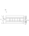
〔調光フィルム〕
図2は、調光フィルムを示す断面図である。この調光フィルム10は、フィルム形状により形成され、合わせガラスに使用される場合の他、例えば調光を図る部位に貼り付けて使用される。なおこのような調光を図る部位に貼り付けて使用される場合は、例えば建築物の窓ガラス、ショーケース、屋内の透明パーテーション等に配置して透過、不透明を切り替える場合等である。
[Light control film]
FIG. 2 is a cross-sectional view showing a light control film. The
この調光フィルム10は、液晶を利用して透過光を制御する調光フィルムであり、フィルム形状による第1及び第2の積層体である下側積層体13(第1の積層体)及び上側積層体12(第2の積層体)により液晶層14を挟持して液晶セル15が作製され、この液晶セル15を直線偏光板16、17により挟持して作成される。
ここでこの実施形態において、液晶層14の駆動には、TN(Twisted Nematic)方式が適用されるものの、例えばVA(Virtical Alignment)方式、IPS(In−Place−Switching)方式等、種々の方式を適用することができる。調光フィルム10には、液晶層14の厚みを一定に保持するためのスペーサー24が下側積層体13及び又は上側積層体12に設けられる。直線偏光板16、17は、それぞれ液晶セル15側に光学補償に供する位相差フィルム18、19が設けられる。積層体12、13は、それぞれ基材21A、21Bに電極22A、22B、配向層23A、23Bを順次作成して形成される。なお位相差フィルム18、19は、必要に応じて省略してもよい。
The
In this embodiment, although the TN (Twisted Nematic) method is applied to drive the liquid crystal layer 14, various methods such as a VA (Virtual Alignment) method and an IPS (In-Place-Switching) method are used. Can be applied. In the
これによりこの調光フィルム10は、電極22A、22Bの印加電圧の可変により、図3に示すように、外来光L1の透過を制御し、透明状態と非透明状態とで状態を切り替えるように構成される。なお図3(A)は、電極22A、22B間に電圧を印加しない状態を示し、図3(B)は、電極22A、22Bに電圧を印加した状態を示し、これによりこの実施形態では、いわゆるノーマリーホワイトにより液晶層14を駆動する。なおこれに代えてノーマリーブラックにより駆動するようにしてもよい。またIPS方式を適用する場合、電極22A、22Bは、配向層23A又は23B側に纏めて作製されることは言うまでも無く、これに対応するように後述する積層体12、13が構成されることになる。
Accordingly, the
なお調光フィルム10は、例えば建築物の窓ガラス、ショーケース、屋内の透明パーテーション等に貼り付けて使用する場合等においては、直線偏光板16及び又は17の、液晶セル15とは逆側の面に、ハードコート層等による保護層が設けられる。
In the case where the
ここで基材21A、21Bは、液晶セル15に適用可能な可撓性を有する各種の透明フィルム材を適用することができ、この実施形態では、両面にハードコート層が作製されてなるポリカーボネートによるフィルム材が適用される。電極22A、22Bは、液晶層14にほぼ均一な電界を印加可能であって、透明と知覚される種々の構成を適用することができるものの、この実施形態では、透明電極材であるITOによる透明導電膜を基材21A、21Bの全面に作製して形成される。なお上述したように、IPS方式等においては、電極は所望の形状によりパターンニングされて作製される。
Here, as the
配向層23A、23Bは、ポリイミド等の配向層に適用可能な各種材料層が適用され、この材料層の表面にラビングロールを使用したラビング処理により微細なライン状凹凸形状を作製して形成される。なおこのようなラビング処理による配向層に代えて、ラビング処理により作製した微細なライン状凹凸形状を賦型処理により作製して配向層を作製してもよく、また光配向層により作製してもよい。 The alignment layers 23A and 23B are formed by applying various material layers applicable to the alignment layer such as polyimide and forming a fine line-shaped uneven shape on the surface of the material layer by rubbing using a rubbing roll. . Instead of the alignment layer formed by the rubbing process, the alignment layer may be formed by forming a fine line-shaped uneven shape formed by the rubbing process by the shaping process, or by using the photo-alignment layer. Good.
スペーサー24は、各種の樹脂材料を広く適用することができるものの、この実施形態ではフォトレジストにより作製される。
なお液晶セル15は、液晶層14を囲むように、シール剤25が配置され、このシール剤25により液晶の漏出が防止される。
The
In the
〔製造工程〕
図4は、液晶セル15の製造工程を示すフローチャートである。液晶セル15は、電極作製工程SP1において、基材21A及び21BにITOによる透明電極22A、22Bが作製される。続くスペーサー作製工程SP3において、スペーサー24に係る塗工液(フォトレジスト)を塗工した後、乾燥、露光して現像することにより、スペーサー24が作製される。なお積層体12、13の一方のみにスペーサー24を作製する場合、スペーサー24を作製しない場合の基材については、スペーサー作製工程SP3が省略される。
〔Manufacturing process〕
FIG. 4 is a flowchart showing the manufacturing process of the
続いて液晶セル15は、配向層材料層作製工程SP4において、配向層23A、23Bに係る塗工液が塗工されて乾燥、硬化されることにより、配向層23A、23Bの材料層が形成される。続いて液晶セル15は、ラビング工程SP5において、ラビングロールを使用したラビング処理により、配向層材料層の表面に微細なライン状凹凸形状が作製されて配向層23A、23Bが作製される。
Subsequently, in the alignment layer material layer manufacturing step SP4, the
続いて液晶セル15は、封止工程SP6において、積層体12、13の一方に、液晶層14を囲む形状によりシール剤25が設けられると共に、このシール剤25により囲まれた箇所に液晶材料が配置される。この工程は、この状態で積層体12、13の他方を持ち来して積層体12、13により液晶材料を挟持するように積層し、この状態で加圧して紫外線の照射等によりシール剤を硬化させ、これにより液晶セル15が作製される。
Subsequently, in the sealing process SP6, the
なお液晶セル15は、基材21A、21Bがロールに巻き取られた長尺フィルム形態により提供され、これら工程SP2〜SP6の全て、又はこれら工程SP2〜SP6のうちの一部が、ロールから基材21A、21Bを引き出して搬送しながら実行される。なおこれにより液晶セル15は、必要に応じて、途中の工程から枚葉の処理により各工程が実行されることになる。
The
〔スペーサーの詳細構成〕
図5は、スペーサー24の詳細構成を説明する図表である。図6は図2のA−A断面の一部を示す図である。図6に示すように、スペーサー24は、シール剤25で囲まれた内部の領域に配置されている。この内部の領域は、調光フィルム1の調光に寄与する調光領域Sである。
スペーサー24は、柱形状により、より具体的には円柱形状又は円錐台形状により、断面円形形状により形成される。
[Detailed configuration of spacer]
FIG. 5 is a chart for explaining the detailed configuration of the
The
スペーサー24は、当該調光フィルム10を正面視した場合の、調光領域Sにおける単位面積当たりのスペーサー24の占有面積の割合(調光フィルム10の一面から見た場合のスペーサー24の投影面積の割合,以下、適宜、スペーサーの占有率と呼ぶ)が、0.5%以上10%以下により、より好ましくは0.5%以上8%以下により配置される。
The
調光フィルム10を合わせガラス1の中間材に使用する場合、合わせガラス1の製造工程の加熱加圧工程における加圧、加熱により、スペーサー24が変形する場合がある。この変形が大きいと、調光フィルム10においては、積層体12、13の電極22A、22Bが短絡して動作しなくなったり、また動作が不安定になる。また液晶層14の厚み(セルギャップ)が局所的に低下して不均一化し、外観品位が低下することになる。
When using the
種々に検討した結果では、このスペーサーの占有率が0.5%未満になるとスペーサー1本当たりに掛かる圧力が大きくなり、スペーサー24が潰れたり、スペーサー24の先端が対向面に貫入して電極を短絡させたりし、またスペーサー24間で基材が撓んでセルギャップが不均一となり、これらにより調光フィルムの動作が不安定になり、また外観品位が低下する。
As a result of various investigations, when the occupation ratio of the spacer is less than 0.5%, the pressure applied to each spacer increases, the
しかしながらスペーサーの占有率が0.5%以上であるようにすれば、このようなスペーサー24の変形による電極22A、22Bが短絡、セルギャップの局所的な低下を防止することができ、これにより安定に動作させて外観品位の低下を防止することができる。
However, if the occupation ratio of the spacer is 0.5% or more, the
これに対してスペーサーの占有率が10%より大きい場合、より好ましくはスペーサーの占有率が8%より大きい場合、スペーサー24の密度が大きくなり過ぎることにより、スペーサー24による各種の不具合が発生する。
On the other hand, when the occupation ratio of the spacer is larger than 10%, more preferably when the occupation ratio of the spacer is larger than 8%, the density of the
スペーサーの占有率が10%より大きい場合、より好ましくはスペーサーの占有率が8%より大きい場合、ラビング処理時にスペーサー24の影となって正常にラビング痕を作製できない部位の面積が増大することになり、その結果、液晶の配向性が低下する。
When the occupancy ratio of the spacer is larger than 10%, more preferably when the occupancy ratio of the spacer is larger than 8%, the area of the portion where the rubbing trace cannot be normally produced increases due to the shadow of the
またスペーサー24が設けられている部位は、何ら液晶が配置されていないことにより、結局、調光フィルム10では、このスペーサー24が設けられている部位では、クロスニコル配置による直線偏光板16、17の積層体の光学特性により透過光を遮光することになる。
スペーサーの占有率が大きくなると、このスペーサー24による透過光の遮光の影響が顕著に知覚されるようになり、その結果、透過性が低下することになる。またスペーサーの占有率が増大すると、回折光が増大し、回折光が光スポット等により見て取られたりすることになる。
In addition, since the liquid crystal is not disposed at the portion where the
When the occupation ratio of the spacer is increased, the effect of blocking the transmitted light by the
具体的に、図5は、スペーサーの占有率の実験結果を示す図表である。この図5において、「×」の印は全てのサンプルで実用に適さない計測結果が得られたことを示し、「△」は、複数サンプルの一部で実用に適さない計測結果が得られたことを示し、「○」は複数サンプルの全てで十分に実用可能である計測結果が得られたことを示す。 Specifically, FIG. 5 is a chart showing experimental results of the occupation ratio of the spacer. In FIG. 5, “×” indicates that measurement results unsuitable for practical use were obtained for all samples, and “Δ” indicates measurement results unsuitable for practical use for a part of a plurality of samples. “◯” indicates that a measurement result that is sufficiently practical for all of the plurality of samples was obtained.
図5に係る実験では、定盤による硬度の高い平滑面に調光フィルムを載置した状態で、0.8MPaに相当する加重を24時間印加した後、セルギャップを観察してスペーサー間の基材の撓み、セルギャップの不均一化(撓み(厚み不均一))を観察した。
このようにして加重を印加した後、上側積層体及び下側積層体を剥離してスペーサーを顕微鏡により観察してスペーサーの潰れ(スペーサー潰れ)を確認し、スペーサーが当接する部位を顕微鏡により観察してスペーサーが当接する部位へのスペーサー先端の貫入、基材の変形(フィルム貫入、基材変形)を観察した。
In the experiment according to FIG. 5, a load corresponding to 0.8 MPa was applied for 24 hours in a state where the light control film was placed on a smooth surface having high hardness by a surface plate, and then the cell gap was observed to observe the base between the spacers. The deformation of the material and the non-uniformity of the cell gap (deflection (thickness nonuniformity)) were observed.
After applying the weight in this way, the upper laminate and the lower laminate are peeled off, and the spacer is observed with a microscope to check for collapse of the spacer (spacer collapse), and the portion where the spacer contacts is observed with a microscope. Then, the penetration of the spacer tip into the part where the spacer abuts and the deformation of the base material (film penetration, base material deformation) were observed.
また透過光の観察により、透過率の低下(透過性)、回折光の程度(透過光回折)、液晶の配向性を観察した。また電極への印加電圧の切替により透過状態と遮光状態とを切り替えて液晶の駆動性(液晶駆動性)を観察し、さらに外観を観察した。 Further, by observing the transmitted light, the decrease in transmittance (transmittance), the degree of diffracted light (transmitted light diffraction), and the orientation of the liquid crystal were observed. Further, the driving state of the liquid crystal (liquid crystal driving property) was observed by switching the transmission state and the light shielding state by switching the voltage applied to the electrodes, and the appearance was further observed.
図5において、比較例1は、スペーサーを直径7μm、高さ6μmにより作製し、ピッチ110μmで直交する2方向に等ピッチで配置した。比較例1は、110×110μm2の領域に1個の割合で直径7μmによるスペーサーを配置し、スペーサーの占有率0.3%により液晶セルを作製して調光フィルムを作製した。
比較例1では、スペーサーの潰れが発生した(スペーサー潰れ)。また部分的に、スペーサー24の先端が対向面に貫入した部位が見られ(貫入、基材変形)、またスペーサー24間で基材が撓んでセルギャップの不均一な部位が確認された(撓み(厚み不均一))。
In FIG. 5, in Comparative Example 1, spacers were produced with a diameter of 7 μm and a height of 6 μm, and arranged at equal pitches in two orthogonal directions with a pitch of 110 μm. In Comparative Example 1, a spacer having a diameter of 7 μm was arranged in a ratio of 110 × 110 μm 2, and a liquid crystal cell was manufactured with a spacer occupation ratio of 0.3% to prepare a light control film.
In Comparative Example 1, the spacer was crushed (spacer crushed). In addition, a part where the tip of the
しかし、比較例1では、スペーサーの占有率が0.3%であることにより、スペーサー24による透過率の低下は無視し得る程度に軽微であり、さらに透過光における回折光の光量も軽微であった。また液晶が局所的に配向不良となったりすることも殆んど無視し得ることが判った。しかし、そもそもスペーサー24間で基材が撓んでセルギャップの不均一な部位が存在することにより、液晶層14を駆動して全面を均一に遮光状態、透光状態に設定することが困難であり、液晶駆動性に問題が残った。また外観不良も確認された。総合の評価として、この比較例1は、実用に適さないことが判った。
However, in Comparative Example 1, since the occupation ratio of the spacer is 0.3%, the decrease in the transmittance due to the
実施例1は、スペーサー24を直径9μm、高さ6μmとし、110μmピッチにより配置し、スペーサーの占有率を0.5%に設定した。実施例2は、スペーサー24を直径27μm、高さ6μmとし、230μmピッチにより配置し、スペーサーの占有率を1%に設定した。実施例3は、スペーサー24を直径28μm、高さ6μmとし、110μmピッチにより配置し、スペーサーの占有率を5%に設定した。実施例4は、スペーサー24を直径35μm、高さ6μmとし、110μmピッチにより配置し、スペーサーの占有率を8%に設定した。実施例5は、スペーサー24を直径39μm、高さ6μmとし、110μmピッチにより配置し、スペーサーの占有率を10%に設定した。
In Example 1, the
これら実施例1〜5では、スペーサーの潰れも観察されず、スペーサー24の先端が対向面に貫入した部位も発見されず、セルギャップの不均一な部位も確認されなかった。
さらにスペーサー24による透過率の低下は無視し得る程度に軽微であり、透過光における回折光の光量も軽微であり、液晶が局所的に配向不良となったりすることも殆んど無視し得ることが判った。
液晶層14を駆動して全面を均一に遮光状態、透光状態に設定できることも確認され、液晶駆動性も十分なことが確認され、また外観も問題とならないことが確認された。
総合の評価として、実施例1〜5は、十分に実用可能であることが判った。
In these Examples 1 to 5, the collapse of the spacer was not observed, the part where the tip of the
Furthermore, the decrease in transmittance due to the
It was confirmed that the liquid crystal layer 14 was driven and the entire surface could be uniformly set in a light-shielding state and a light-transmitting state. It was confirmed that the liquid crystal driving property was sufficient and the appearance was not a problem.
As a comprehensive evaluation, Examples 1 to 5 were found to be sufficiently practical.
これに対して比較例2は、スペーサー24を直径48μm、高さ6μmとし、110μmピッチにより配置し、スペーサーの占有率を15%に設定した。比較例2では、スペーサーの潰れも観察されず、スペーサー24の先端が対向面に貫入した部位も発見されず、またセルギャップの不均一な部位も確認されなかった。
しかし、スペーサー24による透過率の低下は無視できない程度であり、透過光における回折光の光量も無視できない程度であり、液晶の局所的な配向不良も無視できない程度であった。
これに対してセルギャップを安定に保持できていることにより、液晶層14を駆動して全面を均一に遮光状態、透光状態に設定できることは確認され、液晶駆動性は十分なことが確認された。
しかし、回折光等を無視できないことにより、外観不良と判断され、これにより総合の評価として、この比較例2は、実用に適さないことが判った。
On the other hand, in Comparative Example 2, the
However, the decrease in the transmittance due to the
On the other hand, since the cell gap can be stably maintained, it can be confirmed that the liquid crystal layer 14 can be driven to uniformly set the entire surface in the light-shielding state and the light-transmitting state, and the liquid crystal driving property is confirmed to be sufficient. It was.
However, since the diffracted light or the like cannot be ignored, it was determined that the appearance was poor. Thus, as a comprehensive evaluation, it was found that the comparative example 2 is not suitable for practical use.
なおスペーサー24は、使用する液晶層14の液晶材料に応じて必要な液晶層14の厚みに対応する高さにより形成され、より具体的に2μm以上10μm以下の高さにより作製される。これにより調光フィルム10、合わせガラス1は、外観品位の低下を有効に回避して十分に安定に駆動することができ、また透過性の低下、液晶の配向性の低下を有効に回避して回折光が見て取られたりすることが無いようにすることができる。
The
スペーサー24は、ランダムに配置される場合もあることにより、このスペーサーの占有率は、充分に大きな面積の領域によりスペーサー24を配置する部位の面積を計算し、この部位に配置されたスペーサー24の平面視(正面視)に係る断面積の集計値により求められる。
Since the
実施形態において、スペーサー24は、先端が平坦面である正面視、略円形形状(楕円率0.9以上)により形成される。このように略円形形状により作製する場合、何れの方向にラビング処理する場合でも、ラビング処理の影となる部位の大きさの変化を低減することができ、これによりラビング方向の異なる種々の製品を安定に生産することができる。
このように先端が平坦面である正面視、略円形形状により形成することにより、スペーサー24先端での応力集中を低減することができ、その結果、液晶セル作製時にスペーサー24の先端が対向する配向層に突き刺さったりする現象、スペーサー24のつぶれによるセルギャップの不均一化を有効に回避することができる。
In the embodiment, the
By forming the tip with a substantially circular shape in front view with a flat tip, the stress concentration at the tip of the
楕円率0.9以上により作製する場合、スペーサー24は、短径側で、直径9μm以上により作製して、上述の占有率に設定することにより、局所的な応力の集中を充分に緩和することができ、一段と外観品位の低下等を有効に回避することができる。
In the case of manufacturing with an ellipticity of 0.9 or more, the
なお、占有率0.5〜10%の範囲は、全体においてこの範囲であることが好ましいが、調光領域Sのいずれかにおける1mm2の範囲が、この0.5〜10%の範囲であればよい。例えば、少なくとも応力がかかりやすい部分における1mm2の範囲が0.5〜10%であることが好ましく、応力が比較的かかりにくい箇所においては、この範囲より少ない部分が存在していてもよい。 Note that the range of the occupancy ratio of 0.5 to 10% is preferably this range as a whole, but the range of 1 mm 2 in any of the light control regions S may be the range of 0.5 to 10%. That's fine. For example, it is preferable that the range of 1 mm 2 at least in a portion where stress is easily applied is 0.5 to 10%, and in a portion where stress is relatively difficult to be applied, a portion less than this range may exist.
また、スペーサー24は、個数の観点からすると、調光領域S内における半径200μmの範囲内に2個以上30個以下、好ましくは2個以上10個以下配置されていることが好ましい。
Further, from the viewpoint of the number of
調光領域Sにおける半径200μmの範囲内のスペーサー24の個数が2個未満(1個または配置されていない)であると、上述したスペーサー24の占有率が0.5%未満と同様に、スペーサー1本当たりに掛かる圧力が大きくなり、スペーサー24が潰れたり、スペーサー24の先端が対向面に貫入して電極を短絡させたりし、またスペーサー24間で基材が撓んでセルギャップが不均一となり、これらにより調光フィルムの動作が不安定になり、また外観品位が低下する。
When the number of the
しかし、半径200μmの範囲内のスペーサー24の個数が2個以上であると、このようなスペーサー24の変形による電極22A、22Bが短絡、セルギャップの局所的な低下を防止することができ、これにより安定に動作させて外観品位の低下を防止することができる。
However, when the number of the
一方、半径200μmの範囲内のスペーサー24の個数が30個より多いと、スペーサーの占有率が10%より大きい場合と同様に、以下の不具合が発生する。しかし、本実施形態では30個以下であるので以下の不具合は生じない。
例えば、ラビング処理時にスペーサー24の影となって正常にラビング痕を作製できない部位の面積が増大することになり、その結果、液晶の配向性が低下する。
また、スペーサー24が設けられている部位は、何ら液晶が配置されていないことにより、クロスニコル配置による直線偏光板16、17の積層体の光学特性により透過光を遮光することになる。これによりスペーサーの占有率が大きくなると、このスペーサー24による透過光の遮光の影響が顕著に知覚されるようになり、その結果、透過性が低下することになる。またスペーサーの占有率が増大すると、回折光が増大し、回折光が光スポット等により見て取られたりすることになる。
On the other hand, if the number of the
For example, the area of a portion where a rubbing mark cannot be normally formed due to the shadow of the
Further, since no liquid crystal is disposed at the portion where the
〔第2実施形態〕
図7は第2実施形態の調光フィルム100を示す断面図である。第2実施形態と第1実施形態との相違点は、第2実施形態の液晶層114が、ゲストホスト型液晶分子114Aと二色性色素を混合したゲストホスト方式の液晶層114である点である。
[Second Embodiment]
FIG. 7 is a cross-sectional view showing the
第2実施形態では、直線偏光板を省略することができる。ゲストホスト方式とは、二色性色素114Bをゲストホスト型液晶分子114A内に混合し、ゲストホスト型液晶分子114Aの移動に伴い、二色性色素114Bを移動させることで、光の透遮光を制御する方式である。
In the second embodiment, the linearly polarizing plate can be omitted. In the guest host system, the
なお、図7と図2は直線偏光板が設けられていないこと以外同様の図であり、図2と同様の部材は図2と同一の符号を付して説明を省略する。 7 and 2 are similar views except that the linearly polarizing plate is not provided, and members similar to those in FIG. 2 are denoted by the same reference numerals as those in FIG.
図8、図9はゲストホスト方式の液晶層114における、ゲストホスト型液晶分子114Aと二色性色素114Bとの向きを説明する図である。ゲストホスト方式の調光フィルム100は、遮光時、図9に示すように、ゲストホスト型液晶分子114A、二色性色素114Bが一方向に水平配向する。すなわち、液晶組成物、二色性色素114Bの長軸方向が、一方向であって、かつ水平方向となるように作製される。透光時、図9に示すように、ゲストホスト液晶、二色性色素114Bが垂直配向する。すなわち液晶組成物8A、二色性色素114Bの長軸方向が液晶層114の厚み方向となる。
8 and 9 are diagrams for explaining the orientation of the guest-host type
本実施形態においてもスペーサー24は、当該調光フィルム100を正面視した場合の、調光領域Sにおける単位面積当たりの占有率が、0.5%以上10%以下、より好ましくは0.5%以上8%以下により配置される。
Also in this embodiment, the
したがって、スペーサーの占有率が0.5%以上であるので、第1実施形態と同様にスペーサー24の変形による電極22A、22Bが短絡、セルギャップの局所的な低下を防止することができ、これにより安定に動作させて外観品位の低下を防止することができる。
Therefore, since the occupation ratio of the spacer is 0.5% or more, the
また、スペーサーの占有率が10%以下、より好ましくはスペーサーの占有率が8%以下でるので、スペーサー24の密度が大きくなり過ぎることによってスペーサー24による各種の不具合が発生することがない。さらに、ラビング処理時にスペーサー24の影となって正常にラビング痕を作製できない部位の面積が増大して液晶の配向性が低下することがない。
Further, since the occupation ratio of the spacer is 10% or less, and more preferably, the occupation ratio of the spacer is 8% or less, various problems due to the
また、ゲストホスト方式の調光フィルム100は、ギャップ変動に対して、第1実施形態の調光フィルム第1と比べて透過率及び色の変化が少ない。このため、基材が多少曲がってギャップ(液晶層114の厚さ)が変わっても、透過率の差や色ムラが見えにくい。
したがって、第1実施形態においてスペーサー24は、調光領域内における半径200μmの範囲内に2個以上30個以下、好ましくは2個以上10個以下配置されていたが、第2実施形態の調光フィルム100においては、半径200μmの範囲内に1個以上30個以下、好ましくは1個以上10個以下において、基材が多少曲がってギャップ(液晶層114の厚さ)が変わっても、透過率の差や色ムラが見えにくいという効果を達成することができる。
Moreover, the
Therefore, in the first embodiment, the
〔第3実施形態〕
図10は第3実施形態の調光フィルム200を示す断面斜視図である。第3実施形態では、スペーサーとして、いわゆるビーズスペーサー224が用いられる。本実施形態のビーズスペーサー224は球状で、直径は1μm〜20μm、好ましくは3μm〜15μmの範囲が好ましい。なお、図10において図2と同様の部材は図2と同一の符号を付して説明を省略する。
[Third Embodiment]
FIG. 10 is a cross-sectional perspective view showing the
ビーズスペーサー224は、第1実施形態のスペーサー24と同様に、液晶層14の厚みを規定するために設けられる。ビーズスペーサー224は、シリカ等による無機材料による構成、有機材料による構成、これらを組み合わせたコアシェル構造の構成等を広く適用することができる。
The
本実施形態のビーズスペーサー224は球状であるがまた球状による構成の他、円柱形状、角柱形状等によるロッド形状により構成してもよい。ビーズスペーサー224は、電極22A及び電極22B間であれば何処に配置されていてもよい。またビーズスペーサー224は、透明部材により製造されるが、必要に応じて着色した材料を適用して色味を調整するようにしてもよい。
The
ビーズスペーサー224は、湿式/乾式散布に加え、種々の配置方法を広く適用することができる。この実施形態でビーズスペーサー224は、ビーズスペーサー224を樹脂成分と共に溶剤に分散して製造した塗工液を部分的に塗工した後、乾燥、焼成の処理を順次実行することにより、電極22B上にランダムにビーズスペーサー224を配置して移動困難に保持する。
Various arrangement methods can be widely applied to the
ビーズスペーサー224の占有率の下限は第1実施形態よりも小さくてもよく、本実施形態では0.1%以上10%以下、より好ましくは0.2%以上8%以下であり、本実施形態では単位面積(1mm2)当たり300個のビーズスペーサーが配置されており(300個/mm2)、占有率は0.32%である。
第1実施形態におけるフォトレジストにより作製されるスペーサー24に比して、本実施形態のビーズスペーサー224の占有率が低くてもよい理由は、設計上の液晶セルのギャップ(すなわち、スペーサー24の場合はその高さ、ビーズスペーサー224の場合はその直径)に対して、スペーサー24の場合は円柱形状の直径が液晶セルのギャップよりも大きくなり支点数が少なくなる傾向となるが、ビーズスペーサー224の場合は、スペーサー24と同一占有率でも、支点数が相対的に多くなるためである。
The lower limit of the occupation ratio of the
The reason why the occupancy ratio of the
なお、第1実施形態と同様に占有率0.5〜10%の範囲は、全体においてこの範囲であることが好ましいが、調光領域Sのいずれかにおける1mm2の範囲が、この0.5〜10%の範囲であればよい。例えば、少なくとも応力がかかりやすい部分における1mm2の範囲が0.5〜10%であること好ましく、応力が比較的かかりにくい箇所においては、この範囲より少ない部分が存在していてもよい。 As in the first embodiment, the range of the occupation ratio of 0.5 to 10% is preferably this range as a whole, but the range of 1 mm 2 in any one of the light control regions S is 0.5. It may be in the range of -10%. For example, it is preferable that the range of 1 mm 2 at least in a portion where stress is easily applied is 0.5 to 10%, and in a portion where stress is relatively difficult to be applied, a portion less than this range may exist.
図11は、ビーズスペーサー224の分散状態を示した図である。本実施形態のビーズスペーサー224は、第1実施形態のようにフォトレジストを塗工した後、乾燥、露光して現像する場合と異なり、散布により配置するために、規則正しく配列されるわけではない。しかし、本実施形態においてビーズスペーサー224は、濃度や分散性を調整して図11に示すように、面内の任意の点からの200μm範囲のいずれの領域A,Bにおいても少なくとも1つ存在する配置する。
FIG. 11 is a diagram showing a dispersion state of the
図12は比較形態で、面内の任意の点からの200μm範囲内にスペーサーが1つも存在しない領域B’が存在する。この場合、調光フィルムが曲がる部分ではギャップ(液晶層の厚み)が維持できない可能性がある。 FIG. 12 shows a comparative example, in which there is a region B ′ in which no spacer exists within a 200 μm range from an arbitrary point in the plane. In this case, there is a possibility that the gap (the thickness of the liquid crystal layer) cannot be maintained at the portion where the light control film is bent.
しかし、本実施形態では面内の任意の点からの200μm範囲内にスペーサーが1つも存在しない領域が存在しないため、調光フィルム200が曲がる部分においてもギャップ(液晶層の厚み)が維持可能である。
However, in this embodiment, since there is no region where no spacer exists within a 200 μm range from an arbitrary point in the plane, a gap (thickness of the liquid crystal layer) can be maintained even in a portion where the
本実施形態よると、第1実施形態と同様の効果に加え、以下の効果を有する。
ビーズスペーサー224を用いており、ビーズスペーサー224は中心軸が水平な状態で配置されている。したがって、ビーズスペーサー224と配向層23A,23Bとの接触部は、直線に近い状態であり、液晶層14の厚み方向において、配向層23A,23Bとビーズスペーサー224との隙間に液晶分子14Aが存在する。この隙間に存在する液晶分子14Aも調光に寄与するため、占有面積の全てにおいて調光機能が損なわれるわけではなく、調光機能の劣化を小さくすることができる。
さらに、調光フィルム200の厚み方向に力が加わるにつれて、ビーズスペーサー224と基材(配向層23A,23B)との接触面積が大きくなり、押圧力に対する抗力を増加することができる。
なお、第3実施形態においても第2実施形態と同様に液晶セルがゲストホスト方式であっても良い。
According to this embodiment, in addition to the same effects as those of the first embodiment, the following effects are obtained.
A
Furthermore, as the force is applied in the thickness direction of the
In the third embodiment as well, the liquid crystal cell may be a guest-host type as in the second embodiment.
〔他の実施形態〕
以上、本発明の実施に好適な具体的な構成を詳述したが、本発明は、本発明の趣旨を逸脱しない範囲で、上述の実施形態を種々に変更することができる。
[Other Embodiments]
As mentioned above, although the specific structure suitable for implementation of this invention was explained in full detail, this invention can be variously changed in the range which does not deviate from the meaning of this invention.
すなわち上述の実施形態では、フォトレジストによる透明樹脂によりスペーサーを作製する場合について述べたが、本発明はこれに限らず、紫外線硬化性樹脂等の賦型に供する樹脂を使用して、配向層と一体に、又は配向層と個別に、賦型処理により作製する場合にも広く適用することができる。 That is, in the above-described embodiment, the case where the spacer is made of a transparent resin made of a photoresist has been described. However, the present invention is not limited thereto, and a resin used for shaping such as an ultraviolet curable resin is used to form the alignment layer and The present invention can also be widely applied to a case where it is manufactured by a shaping process integrally or separately from the alignment layer.
1 合わせガラス
2、3 板ガラス
4、5 中間層
10,100,200 調光フィルム
12 上側積層体
13 下側積層体
14,114 液晶層
14A 液晶分子
15 液晶セル
16、17 直線偏光板
18、19 位相差フィルム
21A、21B 基材
22A、22B 電極
23A、23B 配向層
24 スペーサー
25 シール剤
114A ゲストホスト型液晶分子
114B 二色性色素
224 ビーズスペーサー
DESCRIPTION OF
Claims (5)
配向層が設けられた第2の積層体と、
前記第1の積層体及び前記第2の積層体により挟持されるとともに液晶分子を含む液晶層と、
前記液晶層に配置された、前記液晶層の厚みを保持するスペーサーと、
前記第1の積層体及び又は前記第2の積層体に設けられた電極とを備え、
前記電極による駆動により前記液晶分子の配向を制御して透過光を制御する調光フィルムにおいて、
前記スペーサーがフォトレジストによる樹脂により形成されたスペーサーであり、
前記液晶層の調光可能領域における、前記調光フィルムを正面視した場合の単位面積当たりの前記スペーサーの占有面積の割合が、0.5%以上10%以下である
調光フィルム。 A first laminate provided with an alignment layer;
A second laminate provided with an alignment layer;
A liquid crystal layer sandwiched between the first laminate and the second laminate and including liquid crystal molecules;
A spacer that is disposed in the liquid crystal layer and maintains the thickness of the liquid crystal layer;
An electrode provided on the first laminate and / or the second laminate,
In the light control film for controlling the transmitted light by controlling the orientation of the liquid crystal molecules by driving with the electrodes,
The spacer is a spacer formed of a photoresist resin;
The light control film in which the ratio of the area occupied by the spacer per unit area when the light control film is viewed from the front in the light controllable region of the liquid crystal layer is 0.5% or more and 10% or less.
請求項1に記載の調光フィルム。 The light control film according to claim 1, wherein two or more spacers are disposed within a radius of 200 μm.
請求項1に記載の調光フィルム。 The light control film according to claim 1, wherein the liquid crystal layer is a guest-host type liquid crystal layer containing a dichroic dye.
請求項3に記載の調光フィルム。 The light control film according to claim 3 , wherein at least one spacer is disposed in a radius of 200 μm.
合わせガラス。 The laminated glass which pinched | interposed the light control film of any one of Claim 1 to 4 with the plate glass.
Priority Applications (6)
| Application Number | Priority Date | Filing Date | Title |
|---|---|---|---|
| KR1020187014980A KR102651739B1 (en) | 2015-11-13 | 2016-11-11 | Illuminated film and laminated glass |
| CN201680066053.0A CN108463768A (en) | 2015-11-13 | 2016-11-11 | Light modulation film and laminated glass |
| EP16864364.1A EP3376281B1 (en) | 2015-11-13 | 2016-11-11 | Light control film and laminated glass |
| US15/775,438 US11809047B2 (en) | 2015-11-13 | 2016-11-11 | Light transmission control film and laminated glass |
| PCT/JP2016/083568 WO2017082403A1 (en) | 2015-11-13 | 2016-11-11 | Light control film and laminated glass |
| US18/219,897 US20230350249A1 (en) | 2015-11-13 | 2023-07-10 | Light control film and laminated glass |
Applications Claiming Priority (2)
| Application Number | Priority Date | Filing Date | Title |
|---|---|---|---|
| JP2015223394 | 2015-11-13 | ||
| JP2015223394 | 2015-11-13 |
Related Child Applications (1)
| Application Number | Title | Priority Date | Filing Date |
|---|---|---|---|
| JP2017142688A Division JP2017187810A (en) | 2015-11-13 | 2017-07-24 | Light control film and laminated glass |
Publications (2)
| Publication Number | Publication Date |
|---|---|
| JP2017097339A JP2017097339A (en) | 2017-06-01 |
| JP6213653B2 true JP6213653B2 (en) | 2017-10-18 |
Family
ID=58817752
Family Applications (7)
| Application Number | Title | Priority Date | Filing Date |
|---|---|---|---|
| JP2016210662A Active JP6213653B2 (en) | 2015-11-13 | 2016-10-27 | Light control film and laminated glass |
| JP2017142688A Pending JP2017187810A (en) | 2015-11-13 | 2017-07-24 | Light control film and laminated glass |
| JP2018117918A Active JP6489272B2 (en) | 2015-11-13 | 2018-06-21 | Light control film and laminated glass |
| JP2019029944A Active JP6825635B2 (en) | 2015-11-13 | 2019-02-22 | Dimming film and laminated glass |
| JP2021001912A Pending JP2021051329A (en) | 2015-11-13 | 2021-01-08 | Light-modulating film and glass laminate |
| JP2022127988A Active JP7435667B2 (en) | 2015-11-13 | 2022-08-10 | Light control film and laminated glass |
| JP2024017805A Pending JP2024050861A (en) | 2015-11-13 | 2024-02-08 | Light control film and laminated glass |
Family Applications After (6)
| Application Number | Title | Priority Date | Filing Date |
|---|---|---|---|
| JP2017142688A Pending JP2017187810A (en) | 2015-11-13 | 2017-07-24 | Light control film and laminated glass |
| JP2018117918A Active JP6489272B2 (en) | 2015-11-13 | 2018-06-21 | Light control film and laminated glass |
| JP2019029944A Active JP6825635B2 (en) | 2015-11-13 | 2019-02-22 | Dimming film and laminated glass |
| JP2021001912A Pending JP2021051329A (en) | 2015-11-13 | 2021-01-08 | Light-modulating film and glass laminate |
| JP2022127988A Active JP7435667B2 (en) | 2015-11-13 | 2022-08-10 | Light control film and laminated glass |
| JP2024017805A Pending JP2024050861A (en) | 2015-11-13 | 2024-02-08 | Light control film and laminated glass |
Country Status (5)
| Country | Link |
|---|---|
| US (1) | US11809047B2 (en) |
| EP (1) | EP3376281B1 (en) |
| JP (7) | JP6213653B2 (en) |
| KR (1) | KR102651739B1 (en) |
| CN (1) | CN108463768A (en) |
Families Citing this family (27)
| Publication number | Priority date | Publication date | Assignee | Title |
|---|---|---|---|---|
| KR102421609B1 (en) * | 2016-06-20 | 2022-07-18 | 다이니폰 인사츠 가부시키가이샤 | Light control film, driving method of light control film, light control member, vehicle |
| WO2019004160A1 (en) * | 2017-06-26 | 2019-01-03 | 大日本印刷株式会社 | Light modulating member, sun visor, and movable body |
| JP7147139B2 (en) * | 2017-07-31 | 2022-10-05 | 大日本印刷株式会社 | Laminated glass manufacturing method |
| WO2019026849A1 (en) * | 2017-07-31 | 2019-02-07 | 大日本印刷株式会社 | Laminated glass and production method for laminated glass |
| JP2019070780A (en) * | 2017-10-11 | 2019-05-09 | 大日本印刷株式会社 | Dimming film, dimming member and vehicle |
| JP7062912B2 (en) * | 2017-10-11 | 2022-05-09 | 大日本印刷株式会社 | Dimming film, dimming member, vehicle, dimming system and driving method of dimming film |
| JP2019070781A (en) * | 2017-10-11 | 2019-05-09 | 大日本印刷株式会社 | Dimming film, dimming member, and vehicle |
| JP7103369B2 (en) | 2017-11-02 | 2022-07-20 | 大日本印刷株式会社 | Laminated glass manufacturing method, laminated glass, dimming film |
| JP7440266B2 (en) * | 2017-11-24 | 2024-02-28 | 大日本印刷株式会社 | Laminated glass, liquid crystal film |
| KR102184388B1 (en) * | 2017-11-28 | 2020-11-30 | 주식회사 엘지화학 | Transmittance variable device and use thereof |
| JP2019101375A (en) * | 2017-12-07 | 2019-06-24 | 大日本印刷株式会社 | Dimming film, dimming member and vehicle |
| EP3742224A4 (en) | 2018-01-17 | 2021-10-13 | Sekisui Chemical Co., Ltd. | Dimming laminate and resin spacer for dimming laminate |
| KR102448828B1 (en) | 2018-01-30 | 2022-09-29 | 다이니폰 인사츠 가부시키가이샤 | Liquid crystal dimming device and manufacturing method thereof |
| US11695904B2 (en) | 2018-07-20 | 2023-07-04 | Dai Nippon Printing Co., Ltd. | Reflective screen and image display device |
| WO2020017591A1 (en) | 2018-07-20 | 2020-01-23 | 大日本印刷株式会社 | Reflective screen and image display device |
| JP7228122B2 (en) * | 2018-08-08 | 2023-02-24 | 大日本印刷株式会社 | Dimmable cell and its manufacturing method, and dimming device and its manufacturing method |
| US20200089031A1 (en) * | 2018-09-19 | 2020-03-19 | Sharp Kabushiki Kaisha | Method of producing liquid crystal panel |
| JP2020064092A (en) * | 2018-10-15 | 2020-04-23 | 三菱電機株式会社 | Stereoscopic display device |
| JP7373124B2 (en) * | 2019-01-25 | 2023-11-02 | 大日本印刷株式会社 | Light control device and its manufacturing method |
| CN111983863A (en) * | 2019-05-24 | 2020-11-24 | 京东方科技集团股份有限公司 | Light-adjusting glass |
| US20210036265A1 (en) * | 2019-07-30 | 2021-02-04 | Apple Inc. | Electronic Device Having Display With Internal Light Reflection Suppression |
| JP7409125B2 (en) | 2020-02-04 | 2024-01-09 | 大日本印刷株式会社 | Light control device and its manufacturing method |
| WO2021261181A1 (en) | 2020-06-25 | 2021-12-30 | 日本化薬株式会社 | Anthraquinone compound, liquid crystal composition for dimming including said compound, and dimming element |
| FR3114266B1 (en) * | 2020-09-18 | 2022-11-18 | Saint Gobain | LAMINATED GLAZING WITH LIQUID CRYSTAL AND UV CUTTING |
| CN116917796A (en) * | 2021-03-05 | 2023-10-20 | 凸版印刷株式会社 | Dimming sheet and dimming device |
| CN116888525A (en) * | 2021-03-05 | 2023-10-13 | 凸版印刷株式会社 | Dimming sheet and dimming device |
| JP2022157684A (en) * | 2021-03-31 | 2022-10-14 | 株式会社ジャパンディスプレイ | optical element |
Family Cites Families (40)
| Publication number | Priority date | Publication date | Assignee | Title |
|---|---|---|---|---|
| JPH0347392A (en) | 1989-07-12 | 1991-02-28 | Natl House Ind Co Ltd | liquid crystal panel |
| JPH03158827A (en) * | 1989-11-17 | 1991-07-08 | I C I Japan Kk | Production of liquid crystal display element |
| JPH0451221A (en) | 1990-06-20 | 1992-02-19 | Ricoh Co Ltd | Liquid crystal display element |
| JPH04293016A (en) | 1991-03-22 | 1992-10-16 | Seiko Instr Inc | Liquid crystal device |
| JPH04366921A (en) | 1991-06-14 | 1992-12-18 | Toyota Motor Corp | Liquid crystal display element with diaphragm |
| JPH06175139A (en) * | 1992-12-09 | 1994-06-24 | Teijin Ltd | Plastic substrate liquid crystal display element and its production |
| JPH06273727A (en) | 1993-03-18 | 1994-09-30 | Sumitomo Electric Ind Ltd | Liquid crystal element and its production |
| JPH0720479A (en) | 1993-07-02 | 1995-01-24 | Sumitomo Electric Ind Ltd | Liquid crystal element and its production |
| JPH08184273A (en) | 1994-12-27 | 1996-07-16 | Ohbayashi Corp | Lighting control glass window |
| JPH11119227A (en) * | 1997-10-13 | 1999-04-30 | Hitachi Ltd | Liquid crystal display device |
| JP3760645B2 (en) * | 1998-11-11 | 2006-03-29 | コニカミノルタホールディングス株式会社 | Manufacturing method of liquid crystal light modulation device |
| US6396559B1 (en) * | 1998-11-17 | 2002-05-28 | Sharp Kabushiki Kaisha | LCD including spacers used in combination with polymer walls |
| EP1072931A3 (en) * | 1999-07-27 | 2002-02-13 | Minolta Co., Ltd. | Liquid crystal display and method of producing a liquid crystal display |
| JP2001042349A (en) | 1999-07-27 | 2001-02-16 | Minolta Co Ltd | Liquid crystal display device |
| JP2001142083A (en) * | 1999-11-17 | 2001-05-25 | Sanyo Electric Co Ltd | Method of producing display device and display device |
| JP2004070069A (en) * | 2002-08-07 | 2004-03-04 | Ricoh Co Ltd | Manufacturing method of laminated substrate, and manufacturing method of laminated liquid crystal display element |
| JP4432356B2 (en) | 2003-04-30 | 2010-03-17 | ソニー株式会社 | Light control device and imaging device |
| US20050068629A1 (en) * | 2003-09-26 | 2005-03-31 | Primal Fernando | Adjustably opaque window |
| US7652743B2 (en) * | 2005-01-20 | 2010-01-26 | Sharp Kabushiki Kaisha | Liquid crystal display element |
| JP2007010843A (en) | 2005-06-29 | 2007-01-18 | Hitachi Displays Ltd | Liquid crystal display panel |
| KR20070079141A (en) | 2006-02-01 | 2007-08-06 | 삼성전자주식회사 | Display panel, method of making the panel and spacer printing apparatus for making the panel |
| TW200815879A (en) * | 2006-09-19 | 2008-04-01 | Ind Tech Res Inst | Liquid crystal EO film with particles having high surface area and method of fabricating the same |
| JP2008102341A (en) * | 2006-10-19 | 2008-05-01 | Fujifilm Corp | Dimming material |
| JP2008256993A (en) * | 2007-04-06 | 2008-10-23 | Hitachi Displays Ltd | Liquid crystal display device and method of manufacturing the same |
| JP2010208861A (en) | 2007-07-03 | 2010-09-24 | Asahi Glass Co Ltd | Toning window material |
| JP2009036967A (en) | 2007-08-01 | 2009-02-19 | Asahi Glass Co Ltd | Light control window material |
| JP2009216976A (en) | 2008-03-11 | 2009-09-24 | Epson Imaging Devices Corp | Liquid crystal device, method of manufacturing liquid crystal device, and electronic device |
| TWI370934B (en) * | 2008-05-08 | 2012-08-21 | Au Optronics Corp | Liquid crystal panel structure and method for manufacturing the same |
| WO2010022294A2 (en) * | 2008-08-20 | 2010-02-25 | Ravenbrick, Llc | Methods for fabricating thermochromic filters |
| JP2011186453A (en) | 2010-02-12 | 2011-09-22 | Semiconductor Energy Lab Co Ltd | Liquid crystal display device |
| CN101957521B (en) | 2010-08-12 | 2013-11-20 | 大连东方科脉电子有限公司 | High-contrast liquid crystal electronic paper displayer and manufacturing method thereof |
| JP2012150206A (en) | 2011-01-18 | 2012-08-09 | Japan Display Central Co Ltd | Liquid crystal shutter |
| JP2014149319A (en) | 2011-06-03 | 2014-08-21 | Sharp Corp | Display device |
| JP5951202B2 (en) | 2011-08-23 | 2016-07-13 | スタンレー電気株式会社 | Liquid crystal display |
| JP2013130746A (en) * | 2011-12-22 | 2013-07-04 | Seiko Electric Co Ltd | Light control element |
| CN104583849B (en) * | 2012-08-27 | 2017-07-18 | 夏普株式会社 | Liquid crystal display device |
| EP2923235B1 (en) | 2012-11-21 | 2021-07-07 | Nexeon Energy Solutions LLC | Energy-efficient film |
| CN102967967B (en) * | 2012-12-14 | 2014-12-17 | 福耀玻璃工业集团股份有限公司 | Method for controlling bonding strength of bonding layers of spacers of dimmer |
| JP6155062B2 (en) | 2013-03-19 | 2017-06-28 | 本田技研工業株式会社 | Light control panel structure and manufacturing method thereof |
| KR20150031126A (en) * | 2013-09-13 | 2015-03-23 | 삼성디스플레이 주식회사 | Liquid crystal display |
-
2016
- 2016-10-27 JP JP2016210662A patent/JP6213653B2/en active Active
- 2016-11-11 EP EP16864364.1A patent/EP3376281B1/en active Active
- 2016-11-11 US US15/775,438 patent/US11809047B2/en active Active
- 2016-11-11 CN CN201680066053.0A patent/CN108463768A/en active Pending
- 2016-11-11 KR KR1020187014980A patent/KR102651739B1/en active IP Right Grant
-
2017
- 2017-07-24 JP JP2017142688A patent/JP2017187810A/en active Pending
-
2018
- 2018-06-21 JP JP2018117918A patent/JP6489272B2/en active Active
-
2019
- 2019-02-22 JP JP2019029944A patent/JP6825635B2/en active Active
-
2021
- 2021-01-08 JP JP2021001912A patent/JP2021051329A/en active Pending
-
2022
- 2022-08-10 JP JP2022127988A patent/JP7435667B2/en active Active
-
2024
- 2024-02-08 JP JP2024017805A patent/JP2024050861A/en active Pending
Also Published As
| Publication number | Publication date |
|---|---|
| JP6825635B2 (en) | 2021-02-03 |
| JP2018205746A (en) | 2018-12-27 |
| KR102651739B1 (en) | 2024-03-28 |
| KR20180082474A (en) | 2018-07-18 |
| JP7435667B2 (en) | 2024-02-21 |
| EP3376281A1 (en) | 2018-09-19 |
| JP2017187810A (en) | 2017-10-12 |
| JP2019144554A (en) | 2019-08-29 |
| JP2017097339A (en) | 2017-06-01 |
| US20180307077A1 (en) | 2018-10-25 |
| JP2021051329A (en) | 2021-04-01 |
| EP3376281B1 (en) | 2024-04-24 |
| EP3376281A4 (en) | 2019-05-08 |
| CN108463768A (en) | 2018-08-28 |
| JP2022145903A (en) | 2022-10-04 |
| JP6489272B2 (en) | 2019-03-27 |
| US11809047B2 (en) | 2023-11-07 |
| JP2024050861A (en) | 2024-04-10 |
Similar Documents
| Publication | Publication Date | Title |
|---|---|---|
| JP6489272B2 (en) | Light control film and laminated glass | |
| CN109073923B (en) | Light-adjusting film, laminated glass and method for manufacturing light-adjusting film | |
| US20230350249A1 (en) | Light control film and laminated glass | |
| JP5910788B1 (en) | Light control film, laminated glass, and method for manufacturing light control film | |
| JP6065142B1 (en) | Light control film, laminated glass, and method for manufacturing light control film | |
| JP5950014B1 (en) | Light control film | |
| JP6665661B2 (en) | Light control film, method for manufacturing light control film | |
| JP6065143B1 (en) | Light control film, laminated glass, and method for manufacturing light control film | |
| JP6156540B1 (en) | Light control film and method of manufacturing light control film | |
| JP6048606B1 (en) | Light control film and method of manufacturing light control film | |
| JP6057012B1 (en) | Light control film | |
| JP2017181825A (en) | Light control film and window | |
| JP2018005040A (en) | Light control film and method for forming the light control film | |
| JP2017198731A (en) | Lighting control film and manufacturing method of lighting control film | |
| JP2018049232A (en) | Liquid crystal cell | |
| JP2017181826A (en) | Light control film and window | |
| JP2017021285A (en) | Dimming material | |
| JP2017198748A (en) | Lighting control film and manufacturing method of lighting control film |
Legal Events
| Date | Code | Title | Description |
|---|---|---|---|
| A621 | Written request for application examination |
Free format text: JAPANESE INTERMEDIATE CODE: A621 Effective date: 20161117 |
|
| A871 | Explanation of circumstances concerning accelerated examination |
Free format text: JAPANESE INTERMEDIATE CODE: A871 Effective date: 20161117 |
|
| A975 | Report on accelerated examination |
Free format text: JAPANESE INTERMEDIATE CODE: A971005 Effective date: 20170110 |
|
| A131 | Notification of reasons for refusal |
Free format text: JAPANESE INTERMEDIATE CODE: A131 Effective date: 20170117 |
|
| A521 | Request for written amendment filed |
Free format text: JAPANESE INTERMEDIATE CODE: A523 Effective date: 20170228 |
|
| A02 | Decision of refusal |
Free format text: JAPANESE INTERMEDIATE CODE: A02 Effective date: 20170425 |
|
| A521 | Request for written amendment filed |
Free format text: JAPANESE INTERMEDIATE CODE: A523 Effective date: 20170724 |
|
| A911 | Transfer to examiner for re-examination before appeal (zenchi) |
Free format text: JAPANESE INTERMEDIATE CODE: A911 Effective date: 20170731 |
|
| TRDD | Decision of grant or rejection written | ||
| A01 | Written decision to grant a patent or to grant a registration (utility model) |
Free format text: JAPANESE INTERMEDIATE CODE: A01 Effective date: 20170822 |
|
| A61 | First payment of annual fees (during grant procedure) |
Free format text: JAPANESE INTERMEDIATE CODE: A61 Effective date: 20170904 |
|
| R150 | Certificate of patent or registration of utility model |
Ref document number: 6213653 Country of ref document: JP Free format text: JAPANESE INTERMEDIATE CODE: R150 |