JP6209826B2 - Lead frame, lead frame with resin, multi-sided body of lead frame, multi-sided body of lead frame with resin, optical semiconductor device, multi-sided body of optical semiconductor device - Google Patents
Lead frame, lead frame with resin, multi-sided body of lead frame, multi-sided body of lead frame with resin, optical semiconductor device, multi-sided body of optical semiconductor device Download PDFInfo
- Publication number
- JP6209826B2 JP6209826B2 JP2013033390A JP2013033390A JP6209826B2 JP 6209826 B2 JP6209826 B2 JP 6209826B2 JP 2013033390 A JP2013033390 A JP 2013033390A JP 2013033390 A JP2013033390 A JP 2013033390A JP 6209826 B2 JP6209826 B2 JP 6209826B2
- Authority
- JP
- Japan
- Prior art keywords
- lead frame
- terminal
- resin
- outer peripheral
- optical semiconductor
- Prior art date
- Legal status (The legal status is an assumption and is not a legal conclusion. Google has not performed a legal analysis and makes no representation as to the accuracy of the status listed.)
- Active
Links
Images


Classifications
-
- H—ELECTRICITY
- H01—ELECTRIC ELEMENTS
- H01L—SEMICONDUCTOR DEVICES NOT COVERED BY CLASS H10
- H01L24/00—Arrangements for connecting or disconnecting semiconductor or solid-state bodies; Methods or apparatus related thereto
- H01L24/93—Batch processes
- H01L24/95—Batch processes at chip-level, i.e. with connecting carried out on a plurality of singulated devices, i.e. on diced chips
- H01L24/97—Batch processes at chip-level, i.e. with connecting carried out on a plurality of singulated devices, i.e. on diced chips the devices being connected to a common substrate, e.g. interposer, said common substrate being separable into individual assemblies after connecting
-
- H—ELECTRICITY
- H01—ELECTRIC ELEMENTS
- H01L—SEMICONDUCTOR DEVICES NOT COVERED BY CLASS H10
- H01L2224/00—Indexing scheme for arrangements for connecting or disconnecting semiconductor or solid-state bodies and methods related thereto as covered by H01L24/00
- H01L2224/01—Means for bonding being attached to, or being formed on, the surface to be connected, e.g. chip-to-package, die-attach, "first-level" interconnects; Manufacturing methods related thereto
- H01L2224/26—Layer connectors, e.g. plate connectors, solder or adhesive layers; Manufacturing methods related thereto
- H01L2224/31—Structure, shape, material or disposition of the layer connectors after the connecting process
- H01L2224/32—Structure, shape, material or disposition of the layer connectors after the connecting process of an individual layer connector
- H01L2224/321—Disposition
- H01L2224/32151—Disposition the layer connector connecting between a semiconductor or solid-state body and an item not being a semiconductor or solid-state body, e.g. chip-to-substrate, chip-to-passive
- H01L2224/32221—Disposition the layer connector connecting between a semiconductor or solid-state body and an item not being a semiconductor or solid-state body, e.g. chip-to-substrate, chip-to-passive the body and the item being stacked
- H01L2224/32245—Disposition the layer connector connecting between a semiconductor or solid-state body and an item not being a semiconductor or solid-state body, e.g. chip-to-substrate, chip-to-passive the body and the item being stacked the item being metallic
-
- H—ELECTRICITY
- H01—ELECTRIC ELEMENTS
- H01L—SEMICONDUCTOR DEVICES NOT COVERED BY CLASS H10
- H01L2224/00—Indexing scheme for arrangements for connecting or disconnecting semiconductor or solid-state bodies and methods related thereto as covered by H01L24/00
- H01L2224/01—Means for bonding being attached to, or being formed on, the surface to be connected, e.g. chip-to-package, die-attach, "first-level" interconnects; Manufacturing methods related thereto
- H01L2224/42—Wire connectors; Manufacturing methods related thereto
- H01L2224/47—Structure, shape, material or disposition of the wire connectors after the connecting process
- H01L2224/48—Structure, shape, material or disposition of the wire connectors after the connecting process of an individual wire connector
- H01L2224/4805—Shape
- H01L2224/4809—Loop shape
- H01L2224/48091—Arched
-
- H—ELECTRICITY
- H01—ELECTRIC ELEMENTS
- H01L—SEMICONDUCTOR DEVICES NOT COVERED BY CLASS H10
- H01L2224/00—Indexing scheme for arrangements for connecting or disconnecting semiconductor or solid-state bodies and methods related thereto as covered by H01L24/00
- H01L2224/01—Means for bonding being attached to, or being formed on, the surface to be connected, e.g. chip-to-package, die-attach, "first-level" interconnects; Manufacturing methods related thereto
- H01L2224/42—Wire connectors; Manufacturing methods related thereto
- H01L2224/47—Structure, shape, material or disposition of the wire connectors after the connecting process
- H01L2224/48—Structure, shape, material or disposition of the wire connectors after the connecting process of an individual wire connector
- H01L2224/481—Disposition
- H01L2224/48151—Connecting between a semiconductor or solid-state body and an item not being a semiconductor or solid-state body, e.g. chip-to-substrate, chip-to-passive
- H01L2224/48221—Connecting between a semiconductor or solid-state body and an item not being a semiconductor or solid-state body, e.g. chip-to-substrate, chip-to-passive the body and the item being stacked
- H01L2224/48245—Connecting between a semiconductor or solid-state body and an item not being a semiconductor or solid-state body, e.g. chip-to-substrate, chip-to-passive the body and the item being stacked the item being metallic
- H01L2224/48247—Connecting between a semiconductor or solid-state body and an item not being a semiconductor or solid-state body, e.g. chip-to-substrate, chip-to-passive the body and the item being stacked the item being metallic connecting the wire to a bond pad of the item
-
- H—ELECTRICITY
- H01—ELECTRIC ELEMENTS
- H01L—SEMICONDUCTOR DEVICES NOT COVERED BY CLASS H10
- H01L2224/00—Indexing scheme for arrangements for connecting or disconnecting semiconductor or solid-state bodies and methods related thereto as covered by H01L24/00
- H01L2224/73—Means for bonding being of different types provided for in two or more of groups H01L2224/10, H01L2224/18, H01L2224/26, H01L2224/34, H01L2224/42, H01L2224/50, H01L2224/63, H01L2224/71
- H01L2224/732—Location after the connecting process
- H01L2224/73251—Location after the connecting process on different surfaces
- H01L2224/73265—Layer and wire connectors
-
- H—ELECTRICITY
- H01—ELECTRIC ELEMENTS
- H01L—SEMICONDUCTOR DEVICES NOT COVERED BY CLASS H10
- H01L2224/00—Indexing scheme for arrangements for connecting or disconnecting semiconductor or solid-state bodies and methods related thereto as covered by H01L24/00
- H01L2224/93—Batch processes
- H01L2224/95—Batch processes at chip-level, i.e. with connecting carried out on a plurality of singulated devices, i.e. on diced chips
- H01L2224/97—Batch processes at chip-level, i.e. with connecting carried out on a plurality of singulated devices, i.e. on diced chips the devices being connected to a common substrate, e.g. interposer, said common substrate being separable into individual assemblies after connecting
-
- H—ELECTRICITY
- H01—ELECTRIC ELEMENTS
- H01L—SEMICONDUCTOR DEVICES NOT COVERED BY CLASS H10
- H01L2924/00—Indexing scheme for arrangements or methods for connecting or disconnecting semiconductor or solid-state bodies as covered by H01L24/00
- H01L2924/013—Alloys
- H01L2924/0132—Binary Alloys
- H01L2924/01322—Eutectic Alloys, i.e. obtained by a liquid transforming into two solid phases
-
- H—ELECTRICITY
- H01—ELECTRIC ELEMENTS
- H01L—SEMICONDUCTOR DEVICES NOT COVERED BY CLASS H10
- H01L2924/00—Indexing scheme for arrangements or methods for connecting or disconnecting semiconductor or solid-state bodies as covered by H01L24/00
- H01L2924/10—Details of semiconductor or other solid state devices to be connected
- H01L2924/11—Device type
- H01L2924/12—Passive devices, e.g. 2 terminal devices
- H01L2924/1204—Optical Diode
- H01L2924/12041—LED
-
- H—ELECTRICITY
- H01—ELECTRIC ELEMENTS
- H01L—SEMICONDUCTOR DEVICES NOT COVERED BY CLASS H10
- H01L2924/00—Indexing scheme for arrangements or methods for connecting or disconnecting semiconductor or solid-state bodies as covered by H01L24/00
- H01L2924/30—Technical effects
- H01L2924/35—Mechanical effects
- H01L2924/351—Thermal stress
Landscapes
- Engineering & Computer Science (AREA)
- Computer Hardware Design (AREA)
- Microelectronics & Electronic Packaging (AREA)
- Power Engineering (AREA)
- Lead Frames For Integrated Circuits (AREA)
- Led Device Packages (AREA)
Description
本発明は、光半導体素子を実装する光半導体装置用のリードフレーム、樹脂付きリードフレーム、リードフレームの多面付け体、樹脂付きリードフレームの多面付け体、光半導体装置、光半導体装置の多面付け体に関するものである。 The present invention relates to a lead frame for an optical semiconductor device on which an optical semiconductor element is mounted, a lead frame with resin, a multi-sided body of a lead frame, a multi-sided body of a lead frame with resin, an optical semiconductor device, and a multi-sided body of an optical semiconductor device. It is about.
従来、LED素子等の光半導体素子は、電気的に絶縁され樹脂層で覆われた2つの端子部を有するリードフレームに固定され、その周囲を透明樹脂層によって覆い、光半導体装置として照明装置等の基板に実装されていた(例えば、特許文献1)。
しかし、このような光半導体装置は、LED素子の発光や、実装した基板の熱等によって、樹脂層及びリードフレームがそれぞれ伸びてしまう場合がある。ここで、リードフレームの端子部は、銅等の導電材料から形成され、樹脂層は、熱可塑性樹脂等から形成されているので、両者の線膨張係数の差によって、樹脂層がリードフレームの端子部から剥離してしまうことがある。
2. Description of the Related Art Conventionally, an optical semiconductor element such as an LED element is fixed to a lead frame having two terminal portions that are electrically insulated and covered with a resin layer, and its periphery is covered with a transparent resin layer. (For example, Patent Document 1).
However, in such an optical semiconductor device, the resin layer and the lead frame may extend due to light emission of the LED element, heat of the mounted substrate, and the like. Here, since the terminal portion of the lead frame is formed of a conductive material such as copper and the resin layer is formed of a thermoplastic resin or the like, the resin layer is a terminal of the lead frame due to the difference in linear expansion coefficient between the two. May peel from the part.
また、このような光半導体装置の中には、端子部を覆う樹脂層が、光半導体素子を囲むようにして、光半導体素子の搭載面から突出するようにリフレクタが形成され、光半導体素子から発光する光の方向等を制御するものがある。このような光半導体装置は、リードフレームのリフレクタが形成される側の面が、その面とは反対側の面に比べ樹脂が多く形成されるため、温度変化が生じた場合において、金属及び樹脂の線膨張率の差によって反りが生じてしまい、上述の剥離現象の発生をより顕著にする場合がある。 Further, in such an optical semiconductor device, a reflector is formed so that a resin layer covering the terminal portion surrounds the optical semiconductor element so as to protrude from the mounting surface of the optical semiconductor element, and light is emitted from the optical semiconductor element. Some control the direction of light. In such an optical semiconductor device, the surface of the lead frame on which the reflector is formed is formed with a larger amount of resin than the surface opposite to the surface. There is a case where warpage occurs due to the difference in the linear expansion coefficient, and the occurrence of the above-described peeling phenomenon becomes more remarkable.
本発明の課題は、各端子部と樹脂層との剥離を抑制することができるリードフレーム、樹脂付きリードフレーム、リードフレームの多面付け体、樹脂付きリードフレームの多面付け体、光半導体装置、光半導体装置の多面付け体を提供することである。 The subject of this invention is the lead frame which can suppress peeling with each terminal part and a resin layer, the lead frame with resin, the multi-sided body of a lead frame, the multi-sided body of the lead frame with resin, an optical semiconductor device, light A multifaceted body of a semiconductor device is provided.
本発明は、以下のような解決手段により、前記課題を解決する。なお、理解を容易にするために、本発明の実施形態に対応する符号を付して説明するが、これに限定されるものではない。また、符号を付して説明した構成は、適宜改良してもよく、また、少なくとも一部を他の構成物に代替してもよい。 The present invention solves the above problems by the following means. In addition, in order to make an understanding easy, although the code | symbol corresponding to embodiment of this invention is attached | subjected and demonstrated, it is not limited to this. In addition, the configuration described with reference numerals may be improved as appropriate, or at least a part thereof may be replaced with another configuration.
第1の発明は、複数の端子部(11、12)を有し、前記端子部のうち少なくとも一つに光半導体素子(2)が接続される光半導体装置(1)に用いられるリードフレーム(10)において、前記端子部は、その外周側面の少なくとも一部に、その表面側及び裏面側の外周縁(p1、p2)よりも外側に突出する凸部(M)を有すること、を特徴とするリードフレームである。
第2の発明は、第1の発明のリードフレーム(10)において、前記凸部(M)は、前記各端子部(11、12)の互いに対向する辺の外周側面に形成されること、を特徴とするリードフレームである。
第3の発明は、第2の発明のリードフレーム(210)において、前記凸部(M)は、前記各端子部(211、212)の互いに対向する辺の外周側面に交互に形成されること、を特徴とするリードフレームである。
第4の発明は、第1の発明から第3の発明までのいずれかのリードフレーム(10)において、前記凸部(M)は、その先端部が、前記端子部(11、12)の厚み方向へ湾曲していること、を特徴とするリードフレームである。
第5の発明は、第1の発明から第4の発明までのいずれかのリードフレーム(10)において、前記凸部(M)は、その先端部が、2以上に分岐していること、を特徴とするリードフレームである。
第6の発明は、第1の発明から第5の発明までのいずれかのリードフレーム(10)において、前記凸部(M)は、その厚みが、前記端子部(11、12)の外周側面との付け根部分からその先端部に向かって太くなるように形成されること、を特徴とするリードフレームである。
A first invention has a plurality of terminal portions (11, 12), and a lead frame (1) used for an optical semiconductor device (1) to which an optical semiconductor element (2) is connected to at least one of the terminal portions. 10), wherein the terminal portion has, on at least a part of the outer peripheral side surface thereof, a convex portion (M) protruding outward from the outer peripheral edges (p1, p2) on the front surface side and the back surface side. Lead frame.
According to a second aspect of the present invention, in the lead frame (10) according to the first aspect, the protrusion (M) is formed on an outer peripheral side surface of each terminal portion (11, 12) facing each other. This is a featured lead frame.
According to a third aspect of the present invention, in the lead frame (210) of the second aspect, the convex portions (M) are alternately formed on the outer peripheral side surfaces of the opposing sides of the terminal portions (211 and 212). The lead frame characterized by the above.
According to a fourth aspect of the present invention, in any one of the lead frames (10) from the first aspect to the third aspect, the protrusion (M) has a tip portion that is the thickness of the terminal portion (11, 12). The lead frame is characterized by being bent in a direction.
According to a fifth aspect of the invention, in any one of the lead frames (10) from the first aspect to the fourth aspect of the invention, the convex part (M) has a tip part branched into two or more. This is a featured lead frame.
According to a sixth invention, in any one of the lead frames (10) from the first invention to the fifth invention, the convex portion (M) has an outer peripheral side surface of the terminal portion (11, 12). The lead frame is characterized in that the lead frame is formed so as to become thicker from the base part toward the tip part.
第7の発明は、第1の発明から第6の発明までのいずれかのリードフレーム(10)と、前記リードフレームの前記端子部(11、12)の外周側面及び前記端子部間に形成されるフレーム樹脂部(20a)を有する樹脂層(20)と、を備える樹脂付きリードフレームである。
第8の発明は、第7の発明の樹脂付きリードフレームにおいて、前記樹脂層(20)は、前記リードフレーム(10)の前記光半導体素子(1)が接続される側の面に突出して形成されるリフレクタ樹脂部(20b)を有すること、を特徴とする樹脂付きリードフレームである。
The seventh invention is formed between any one of the lead frames (10) from the first invention to the sixth invention and the outer peripheral side surface of the terminal portion (11, 12) of the lead frame and the terminal portion. And a resin layer (20) having a frame resin portion (20a).
According to an eighth aspect of the present invention, in the lead frame with resin of the seventh aspect, the resin layer (20) is formed to project from a surface of the lead frame (10) on the side to which the optical semiconductor element (1) is connected. It is a lead frame with resin characterized by having the reflector resin part (20b) to be performed.
第9の発明は、第1の発明から第6の発明までのいずれかのリードフレーム(10)が枠体(F)に多面付けされていること、を特徴とするリードフレームの多面付け体(MS)である。 A ninth aspect of the present invention is a lead frame multi-faced body characterized in that any one of the lead frames (10) from the first aspect to the sixth aspect of the invention is multi-faced to the frame body (F). MS).
第10の発明は、第7の発明又は第8の発明の樹脂付きリードフレームが多面付けされていること、を特徴とする樹脂付きリードフレームの多面付け体(R)である。 A tenth aspect of the present invention is a multi-faced body (R) for a resin-attached lead frame, characterized in that the lead-frame with resin of the seventh or eighth aspect is multi-faced.
第11の発明は、第7の発明又は第8の発明の樹脂付きリードフレームと、前記樹脂付きリードフレームの前記端子部(11、12)のうち少なくとも一つに接続される光半導体素子(2)と、前記樹脂付きリードフレームの前記光半導体素子が接続される側の面に形成され、前記光半導体素子を覆う透明樹脂層(30)と、を備える光半導体装置(1)である。 The eleventh invention is an optical semiconductor element (2) connected to at least one of the lead frame with resin of the seventh or eighth invention and the terminal portions (11, 12) of the lead frame with resin. ) And a transparent resin layer (30) formed on the surface of the lead frame with resin to which the optical semiconductor element is connected, and covering the optical semiconductor element (1).
第12の発明は、第11の発明の光半導体装置(1)が多面付けされていること、を特徴とする光半導体装置の多面付け体である。 A twelfth aspect of the present invention is a multifaceted body of an optical semiconductor device characterized in that the optical semiconductor device (1) of the eleventh aspect is multifaceted.
本発明によれば、リードフレーム、樹脂付きリードフレーム、リードフレームの多面付け体、樹脂付きリードフレームの多面付け体、光半導体装置、光半導体装置の多面付け体は、端子部から樹脂層が剥離してしまうのを抑制することができる。 According to the present invention, a lead frame, a lead frame with a resin, a multi-sided body of a lead frame, a multi-sided body of a lead frame with a resin, an optical semiconductor device, and a multi-sided body of an optical semiconductor device have a resin layer peeled from a terminal portion. Can be suppressed.
(第1実施形態)
以下、図面等を参照して、本発明の第1実施形態について説明する。
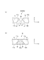
図1は、第1実施形態の光半導体装置1の全体構成を示す図である。
図1(a)は、光半導体装置1の平面図を示し、図1(b)は、光半導体装置1の側面図を示し、図1(c)は、光半導体装置1の裏面図を示す。図1(d)は、図1(a)のd−d断面図を示す。
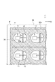
図2は、第1実施形態のリードフレームの多面付け体MSの詳細を説明する図である。
図2(a)、図2(b)は、それぞれリードフレームの多面付け体MSの平面図、裏面図を示し、図2(c)、図2(d)は、それぞれ図2(a)のc−c断面図、d−d断面図を示す。
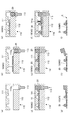
図3は、第1実施形態の光反射樹脂層20が形成された樹脂付きリードフレームの多面付け体Rの詳細を説明する図である。
図3(a)、図3(b)は、それぞれ、樹脂付きリードフレームの多面付け体Rの平面図、裏面図を示し、図3(c)、図3(d)は、それぞれ図3(a)のc−c断面図と、d−d断面図を示す。
図4は、第1実施形態のリードフレーム10の端子部間の断面の詳細を説明する図である。図4(a)は、図2(c)のA部詳細を示す図であり、図4(b)は、図3(c)のB部詳細を示す図である。
各図において、光半導体装置1の平面図における左右方向をX方向、上下方向をY方向、厚み方向をZ方向とする。
(First embodiment)
Hereinafter, a first embodiment of the present invention will be described with reference to the drawings and the like.
FIG. 1 is a diagram illustrating an overall configuration of an
FIG. 1A shows a plan view of the
FIG. 2 is a diagram illustrating details of the multi-faced body MS of the lead frame according to the first embodiment.
2 (a) and 2 (b) show a plan view and a back view of the multi-faced body MS of the lead frame, respectively, and FIGS. 2 (c) and 2 (d) respectively show FIG. 2 (a). A cc sectional view and a dd sectional view are shown.
FIG. 3 is a diagram for explaining the details of the multifaceted body R of the lead frame with resin on which the light reflecting
3 (a) and 3 (b) show a plan view and a back view of the multifaceted body R of the lead frame with resin, respectively, and FIG. 3 (c) and FIG. 3 (d) respectively show FIG. The cc sectional view of a) and the dd sectional view are shown.
FIG. 4 is a diagram illustrating details of a cross section between the terminal portions of the
In each figure, the horizontal direction in the plan view of the
光半導体装置1は、外部機器等の基板に取り付けられることによって、実装したLED素子2が発光する照明装置である。光半導体装置1は、図1に示すように、LED素子2(光半導体素子)、リードフレーム10、光反射樹脂層20(樹脂層)、透明樹脂層30を備える。
光半導体装置1は、多面付けされたリードフレーム10(リードフレームの多面付け体MS、図2参照)に光反射樹脂層20を形成して樹脂付きリードフレームの多面付け体R(図3参照)を作製し、LED素子2を電気的に接続し、透明樹脂層30を形成して、パッケージ単位に切断(ダイシング)することによって製造される(詳細は後述する)。
LED素子2は、発光層として一般に用いられるLED(発光ダイオード)の素子であり、例えば、GaP、GaAs、GaAlAs、GaAsP、AlInGaP等の化合物半導体単結晶、又は、InGaN等の各種GaN系化合物半導体単結晶からなる材料を適宜選ぶことにより、紫外光から赤外光に渡る発光波長を選択することができる。
The
In the
The
リードフレーム10は、一対の端子部、すなわち、LED素子2が載置、接続される端子部11と、ボンディングワイヤ2aを介してLED素子2に接続される端子部12とから構成される。
端子部11、12は、それぞれ導電性のある材料、例えば、銅、銅合金、42合金(Ni40.5%〜43%のFe合金)等により形成されており、本実施形態では、熱伝導及び強度の観点から銅合金から形成されている。
端子部11、12は、図2に示すように、互いに対向する辺の間に空隙部Sが形成されており、電気的に独立している。端子部11、12は、1枚の金属基板(銅板)をプレス又はエッチング加工することにより形成されるため、両者の厚みは同等である。
The
Each of the
As shown in FIG. 2, the
端子部11は、図1に示すように、その表面にLED素子2が載置、接続されるLED端子面11aが形成され、また、その裏面に外部機器に実装される外部端子面11bが形成される、いわゆるダイパッドを構成する。端子部11は、LED素子2が載置されるため、端子部12に比べ、その外形が大きく形成されている。
端子部12は、その表面にLED素子2のボンディングワイヤ2aが接続されるLED端子面12aが形成され、また、その裏面に外部機器に実装される外部端子面12bが形成される、いわゆるリード側端子部を構成する。
端子部11、12は、その表面及び裏面にめっき層Cが形成されており(図6(e)参照)、表面側のめっき層Cは、LED素子2の発する光を反射する反射層としての機能を有し、裏面側のめっき層Cは、外部機器に実装されるときの半田の溶着性を高める機能を有する。
As shown in FIG. 1, the
The
The
端子部11、12は、図2に示すように、それぞれの表面の連結部13を除く外周部分がLED端子面11a、12aに窪みが形成され、また、それぞれの裏面の外周部分の全体が外部端子面11b、12bに窪みが形成されている。そのため、端子部11、12は、図4(a)に示すように、それぞれ連結部13を除いた外周側面に、表面側の外周縁p1及び裏面側の外周縁p2よりも外側(各端子部の中央とは反対側)に突出する凸部Mが形成される。
また、本実施形態では、端子部11、12は、表面側の外周縁p1が、裏面側の外周縁p2よりも外側に形成されている。すなわち、各端子部11、12は、図2に示すように、表面側のLED端子面11a、12aの方が、裏面側の外部端子面11b、12bに比べ面積が広くなるように形成される。
ここで、各端子部11、12の表面側の外周縁p1とは、各端子部の表面(LED端子面11a、12a)と外周側面との境界をいい、また、裏面側の外周縁p2とは、各端子部の裏面(外部端子面11b、12b)と外周側面との境界をいう。
As shown in FIG. 2, the
Moreover, in this embodiment, the
Here, the outer peripheral edge p1 on the front surface side of each
凸部Mは、図4(a)に示すように、その断面が略三角形状に形成され、その外周縁p3が、各端子部の表面側の外周縁p1及び裏面側の外周縁p2よりも外側に位置するように形成されている。また、本実施形態では、凸部Mは、各端子部11、12の厚み方向(Z方向)において、外周側面のほぼ中央に形成される例を示すがこれに限定されるものでなく、表面側又は裏面側に偏るようにして形成してもよい。
リードフレーム10は、端子部11、12の周囲や、端子部11、12間の空隙部S等に、光反射樹脂層20を形成する樹脂が充填される場合に、図3に示すように、凸部Mの表面及び裏面にも樹脂が充填され、光反射樹脂層20と各端子部11、12との接触面積を大きくしている。また、図4(b)に示すように、凸部Mが存在することによって、厚み方向において、光反射樹脂層20がリードフレーム10を挟み込む構成にすることができる。
As shown in FIG. 4A, the convex portion M has a substantially triangular cross section, and the outer peripheral edge p3 is more than the outer peripheral edge p1 on the front surface side and the outer peripheral edge p2 on the back surface side of each terminal portion. It is formed so as to be located outside. Moreover, in this embodiment, although the convex part M shows the example formed in the approximate center of an outer peripheral side surface in the thickness direction (Z direction) of each
As shown in FIG. 3, when the
これにより、凸部Mは、厚み方向において、光反射樹脂層20がリードフレーム10から剥離し、抜けてしまうのを抑制するとともに、端子部11、12の水平面内(XY面内)において、光反射樹脂層20が各端子部11、12から剥離してしまうのを抑制する。特に、各端子部の表面側の外周縁p1が、裏面側の外周縁p2よりも外側に形成されているので、光反射樹脂層20は、リードフレーム10の表面側に対する抜けをより効果的に抑制することができる。ここで、凸部Mの表面とは、各端子部の表面側の凸部の傾斜した面をいい、凸部Mの裏面とは、各端子部の裏面側の凸部の傾斜した面をいう。
As a result, the convex portion M suppresses the light reflecting
連結部13は、枠体F内に多面付けされた各リードフレーム10の端子部11、12を、隣接する他のリードフレーム10の端子部や、枠体Fに連結している。連結部13は、多面付けされた各リードフレーム10上にLED素子2等が搭載され、光半導体装置1の多面付け体(図8参照)が形成された場合に、リードフレーム10を形成する外形線(図3(a)及び図3(b)中の破線)でダイシング(切断)される。
連結部13は、端子部11、12を形成する各辺のうち、端子部11、12が対向する辺を除いた辺に形成されている。
The connecting
The
具体的には、連結部13aは、図2(a)に示すように、端子部12の右(+X)側の辺と、右側に隣接する他のリードフレーム10の端子部11の左(−X)側の辺とを接続し、また、端子部11の左側の辺と、左側に隣接する他のリードフレーム10の端子部12の右側の辺とを接続している。枠体Fに隣接する端子部11、12に対しては、連結部13aは、端子部11の左側の辺又は端子部12の右側の辺と、枠体Fとを接続している。
Specifically, as shown in FIG. 2A, the connecting
連結部13bは、端子部11の上(+Y)側の辺と、上側に隣接する他のリードフレーム10の端子部11の下(−Y)側の辺とを接続し、また、端子部11の下側の辺と、下側に隣接する他のリードフレーム10の端子部11の上側の辺とを接続する。枠体Fに隣接する端子部11に対しては、連結部13bは、端子部11の上側又は下側の辺と、枠体Fとを接続している。
連結部13cは、端子部12の上側の辺と、上側に隣接する他のリードフレーム10の端子部12の下側の辺とを接続し、また、端子部12の下側の辺と、下側に隣接する他のリードフレーム10の端子部12の上側の辺とを接続する。枠体Fに隣接する端子部12に対しては、連結部13cは、端子部12の上側又は下側の辺と、枠体Fとを接続している。
The connecting
The connecting
なお、端子部11、12は、連結部13によって、隣り合う他のリードフレーム10の端子部11、12と電気的に導通されるが、光半導体装置1の多面付け体を形成した後に、光半導体装置1(リードフレーム10)の外形(図2(a)の破線)に合わせて各連結部13を切断(ダイシング)することによって絶縁される。また、個片化された場合に、各々の個片を同じ形状にすることができる。
The
連結部13は、図2(b)、図2(c)に示すように、端子部11、12の厚みよりも薄く、かつ、その表面が端子部11、12の表面と同一平面内に形成されている。具体的には、連結部13は、その裏面が、各端子部11、12の裏面の外周部分の窪みと略同一面内に形成されている。これにより、光反射樹脂層20の樹脂が充填された場合に、図3(b)、図3(c)に示すように、連結部13の裏面にも樹脂が流れ込み、光反射樹脂層20がリードフレーム10から剥離してしまうのを抑制することができる。
また、光反射樹脂層20が形成されたリードフレーム10の裏面には、図3(b)に示すように、矩形状の外部端子面11b、12bが表出することとなり、光半導体装置1の外観を向上させることができることに加え、半田で基板に実装する場合に、基板側への半田印刷を容易にしたり、半田を均一に塗布したり、リフロー後に半田内へのボイドの発生を抑制したりすることができる。また、光半導体装置1の面内(XY平面内)の中心線に対して線対称であることから、熱応力等に対する信頼性を向上させることができる。
2B and 2C, the connecting
Further, as shown in FIG. 3B, rectangular external terminal surfaces 11 b and 12 b are exposed on the back surface of the
更に、樹脂付きリードフレームの裏面には、連結部13は表出せず、外部端子面11b、12bのみが表出するので、連結部13の裏面が表出する場合に比べて樹脂付きリードフレームの裏面における金属部分と光反射樹脂層20との界面の長さを短くすることができる。かかる境界は、光反射樹脂層20と端子部とが剥離した場合に隙間になるため、光半導体装置1の内部に水分や、半田のフラックス等が浸入する要因となる。そのため、上述のようにその界面の長さを短くすることによって、光半導体装置1における水分等の浸入経路を減少させることができる。
リードフレームの多面付け体MSは、上述のリードフレーム10を枠体F内に多面付けしたものをいう。枠体Fは、多面付けされたリードフレーム10を固定する部材であり、その外形が矩形状に形成されている。
Further, the connecting
The multi-faced body MS of the lead frame refers to a structure in which the above-described
光反射樹脂層20は、図3に示すように、フレーム樹脂部20aと、リフレクタ樹脂部20bとから構成される。
フレーム樹脂部20aは、端子部11、12の外周側面(リードフレーム10の外周や、空隙部S)だけでなく、各端子部に設けられた凸部Mの表裏面や、連結部13の裏面にも形成される。
As shown in FIG. 3, the light reflecting
The
リフレクタ樹脂部20bは、リードフレーム10の表面側(リードフレーム10のLED素子2が接続される側)に突出するように形成され、リードフレーム10に接続されるLED素子2から発光する光の方向等を制御するリフレクタを構成する。このリフレクタ樹脂部20bは、端子部11、12のLED端子面11a、12aを囲むようにして、リードフレーム10の表面側に突出しており、LED端子面11aに接続されるLED素子2から発光する光を反射させて、光半導体装置1から光を効率よく照射させる。
The
リフレクタ樹脂部20bは、リードフレーム10の多面付け体MSの状態において、その外形が、枠体Fの内周縁に沿うようにして形成されており、その厚み(高さ)寸法が、LED端子面11aに接続されるLED素子2の厚み寸法よりも大きい寸法で形成される。リフレクタ樹脂部20bは、端子部11、12の外周縁に形成されたフレーム樹脂部20aの表面上に重なっており、フレーム樹脂部20aと結合している。
The
ここで、リードフレーム10は銅などの金属により形成され、光反射樹脂層20は熱硬化性樹脂等の樹脂により形成され、また、両者の材料の線膨張率には差がある。そのため、光反射樹脂層20が形成されたリードフレーム10(樹脂付きリードフレーム)は、各端子部に外部機器との半田溶着による熱や、LED素子2の発光による熱が加わることによって、各端子部と光反射樹脂層20との間で剥離が生じてしまう場合がある。
また、リードフレーム10は、上述したように表面側にリフレクタ樹脂部20bが形成されることから裏面側に比べ表面側に樹脂が多く形成される。そのため、樹脂付きリードフレームは、上記熱が加わったり、冷えたりすることで、上述の線膨張率の差によって反りが生じたり、その反りが戻ったりして、これが繰り返されると、上記剥離がより発生しやすくなる。
Here, the
In addition, since the
また、金型に樹脂を流し込む成形方法を用いた場合、線膨張率の差だけでなく、成形収縮や、樹脂の密度、樹脂中のフィラーや高分子の高次構造による異方性、樹脂の結晶性の温度依存、クリープや応力緩和により、リードフレーム10と光反射樹脂層20とが剥離するような応力が残るため、剥離が発生しやすい。
更に、熱可塑性の樹脂を用いた場合、熱可塑性維持のために熱により反応が進むアクリル基、水酸基、エポキシ基、アミン、カルボニル基の様な反応性基を導入することが難しく、リードフレーム10との化学的接着を得るためにこれらの反応性基を導入することが難しい事から、リードフレーム10と光反射樹脂層20との剥離が発生しやすい。
更にまた、熱可塑性の樹脂を形成後に電子線で硬化させる電子線硬化樹脂を用いた場合、熱可塑性維持のためにリードフレームとの化学的接着が得られないことに加え、樹脂成形体に電子線を照射して重合を行うために硬化収縮が発生し、リードフレーム10と光反射樹脂層20との剥離がより生じやすい。
In addition, when a molding method in which a resin is poured into a mold is used, not only the difference in linear expansion coefficient, but also molding shrinkage, resin density, anisotropy due to higher order structures of fillers and polymers in the resin, Due to the temperature dependence of crystallinity, creep, and stress relaxation, a stress that peels off the
Further, when a thermoplastic resin is used, it is difficult to introduce a reactive group such as an acryl group, a hydroxyl group, an epoxy group, an amine, or a carbonyl group, in which the reaction proceeds by heat in order to maintain thermoplasticity. Since it is difficult to introduce these reactive groups in order to obtain a chemical bond with the
Furthermore, when an electron beam curable resin that is cured with an electron beam after forming a thermoplastic resin is used, chemical adhesion with the lead frame is not obtained in order to maintain thermoplasticity, and the resin molded body has an electron. Curing shrinkage occurs because polymerization is performed by irradiating a wire, and peeling between the
特に、リードフレーム10の端子部11、12間は、端子部11、12と光反射樹脂層20との接合面積が狭いため、接合強度が弱く、剥離の発生が顕著となる。樹脂付きリードフレームの端子部間にこの剥離が発生した場合、光半導体装置1の製造過程において、透明樹脂層30を形成する際に、硬化前の液状樹脂が樹脂付きリードフレームの裏面に漏れてしまい、透明樹脂層30を適正に形成することができなかったり、裏面の端子部を漏れた透明樹脂で覆ってしまったりする問題が発生する可能性がある。また、製造した光半導体装置1の端子部間においてこの剥離が発生した場合、端子部間で光半導体装置1が折れて破損する可能性がある。また、光半導体装置1の雰囲気中の水分や、外部端子面に溶着する半田のフラックス等が、剥離した隙間に浸入してしまい、各端子部の表面のめっき層や、光反射樹脂層20、透明樹脂層30等を変色させてしまう可能性がある。
In particular, between the
上記剥離の一因となる反りを抑制するために、光反射樹脂層20の樹脂中に特定のフィラー(粉末)を含有させて線膨張率を、リードフレーム10の金属に近づけることも可能である。しかし、光反射樹脂層20の光反射特性を維持するために、フィラーの含有量は制限されてしまい、樹脂の線膨張率を十分に金属に近づけられない場合がある。また、樹脂に熱可塑性樹脂を使用した場合は、熱可塑性を維持するために三次元架橋密度を上げられないという分子構造上、フィラーを多量に充填した場合に強度が保てないことから、実用レベルとしては線膨張率の調整自体をすることが困難となる。
In order to suppress the warp that contributes to the peeling, it is possible to make the linear expansion coefficient closer to the metal of the
そのため、本実施形態では、リードフレーム10は、各端子部11、12の外周側面に凸部Mが設けられ、リードフレーム10から光反射樹脂層20が剥離してしまうのを抑制することができ、上記光半導体装置1の破損や、変色等の問題の発生を抑制することができる。
また、特にリードフレーム10の各端子部11、12間に対しては、図4(b)に示すように、空隙部Sにおいて各端子部の凸部Mが互いに対向することとなる。そのため、リードフレーム10は、空隙部Sの平面視において、空隙部Sの幅を狭く、すなわち、厚み方向において端子部間の樹脂のみが存在する部分を減らすことができ、製造された光半導体装置1(樹脂付きリードフレーム)の端子部間の強度を向上させることができる。
Therefore, in the present embodiment, the
In particular, between the
光反射樹脂層20は、リードフレーム10に載置されるLED素子2の発する光を反射させるために、光反射特性を有する熱可塑性樹脂や、熱硬化性樹脂が用いられる。
光反射樹脂層20を形成する樹脂は、窪んだ部分への樹脂充填に関しては、樹脂形成時には流動性が高いことが、窪んだ部分での接着性に関しては、分子内に反応基を導入しやすいためにリードフレームとの化学接着性を得られることが必要なため、熱硬化性樹脂が望ましい。
例えば、熱可塑性樹脂としては、ポリアミド、ポリフタルアミド、ポリフェニレンサルファイド、液晶ポリマー、ポリエーテルサルホン、ポリブチレンテレフタレート、ポリオレフィン等を用いることができる。
また、熱硬化性樹脂としては、シリコーン、エポキシ、ポリエーテルイミド、ポリウレタン及びポリブチレンアクリレート等を用いることができる。
さらに、これらの樹脂中に光反射材として、二酸化チタン、二酸化ジルコニウム、チタン酸カリウム、窒化アルミニウム及び窒化ホウ素のうちいずれかを添加することによって、光の反射率を増大させることができる。
また、ポリオレフィンなどの熱可塑性樹脂を成形した後に、電子線を照射することで架橋させる方法を用いた、いわゆる電子線硬化樹脂を用いてもよい。
光反射樹脂層20を形成する樹脂が、リードフレームの多面付け体MSに多面付けされるリードフレーム10に充填されることによって、樹脂付きリードフレームが多面付けされた樹脂付きリードフレームの多面付け体Rが形成される。
The light reflecting
The resin that forms the light reflecting
For example, as the thermoplastic resin, polyamide, polyphthalamide, polyphenylene sulfide, liquid crystal polymer, polyether sulfone, polybutylene terephthalate, polyolefin, or the like can be used.
As the thermosetting resin, silicone, epoxy, polyetherimide, polyurethane, polybutylene acrylate, or the like can be used.
Furthermore, the reflectance of light can be increased by adding any of titanium dioxide, zirconium dioxide, potassium titanate, aluminum nitride, and boron nitride as a light reflecting material to these resins.
Moreover, after molding a thermoplastic resin such as polyolefin, a so-called electron beam curable resin using a method of crosslinking by irradiation with an electron beam may be used.
The resin for forming the light-reflecting
透明樹脂層30は、リードフレーム10上に載置されたLED素子2を保護するとともに、発光したLED素子2の光を外部に透過させるために設けられた透明又は略透明に形成された樹脂層である。透明樹脂層30は、図1に示すように、光反射樹脂層20のリフレクタ樹脂部20bによって囲まれたLED端子面11a、12a上に形成される。
透明樹脂層30は、光の取り出し効率を向上させるために、LED素子2の発光波長において光透過率が高く、また、屈折率が高い材料を選択するのが望ましい。例えば、耐熱性、耐光性、及び機械的強度が高いという特性を満たす樹脂として、エポキシ樹脂や、シリコーン樹脂を選択することができる。特に、LED素子2に高輝度LED素子を用いる場合、透明樹脂層30は、強い光にさらされるため、高い耐光性を有するシリコーン樹脂からなることが好ましい。また、波長変換用の蛍光体を使用してもよく、透明樹脂に分散させてもよい。
The
For the
次に、本実施形態の光半導体装置1の他の形態について説明する。
図5は、第1実施形態の光半導体装置1の他の形態を説明する図である。
図5(a)は、光半導体装置1の平面図を示し、図5(b)は、光半導体装置1の側面図を示し、図5(c)は、光半導体装置1の裏面図を示す。
上述の説明では、リードフレーム10の表面にリフレクタ樹脂部20bが形成される、いわゆるカップ型の光半導体装置1の例で説明したが、本発明は、図5に示すように、リードフレーム10と光反射樹脂層20との厚みがほぼ同等となる、いわゆるフラットタイプの光半導体装置1に適用してもよい。
Next, another form of the
FIG. 5 is a diagram illustrating another form of the
FIG. 5A shows a plan view of the
In the above description, the example of the so-called cup-type
次に、リードフレーム10の製造方法について説明する。
図6は、第1実施形態のリードフレーム10の製造過程を説明する図である。
図6(a)は、レジストパターンを形成した金属基板100を示す平面図と、その平面図のa−a断面図とを示す。図6(b)は、エッチング加工されている金属基板100を示す図である。図6(c)は、エッチング加工後の金属基板100を示す図である。図6(d)は、レジストパターンが除去された金属基板100を示す図である。図6(e)は、めっき処理が施された金属基板100を示す図である。
図7は、第1実施形態のリードフレーム10の他の製造過程を説明する図である。図7(a)は、レジストパターンを形成した金属基板100を示す。図7(b)は、表面がエッチング加工された金属基板100を示す図である。図7(c)は、表面に再度レジストパターンを形成した金属基板100を示す図である。図7(d)は、裏面がエッチング加工された金属基板100を示す図である。図7(e)は、レジストパターンが除去された金属基板100を示す図である。
なお、図6、図7においては、1枚のリードフレーム10の製造過程について図示するが、実際には、1枚の金属基板100からリードフレームの多面付け体MSが製造される。また、図7(a)〜(e)は、それぞれ図6(a)の断面図に基づくものである。
Next, a method for manufacturing the
FIG. 6 is a diagram for explaining the manufacturing process of the
FIG. 6A shows a plan view showing a
FIG. 7 is a diagram for explaining another manufacturing process of the
6 and 7, the manufacturing process of one
リードフレーム10の製造において、金属基板100を加工してリードフレーム10を形成するが、その加工は、プレス加工でも良いが、薄肉部を形成しやすいエッチング処理が望ましい。以下にエッチング処理によるリードフレーム10の製造方法について説明する。
In the manufacture of the
まず、平板状の金属基板100を用意し、図6(a)に示すように、その表面及び裏面のエッチング加工を施さない部分にレジストパターン40a、40bを形成する。なお、レジストパターン40a、40bの材料及び形成方法は、エッチング用レジストとして従来公知の技術を用いることができるが、アクリル系、カゼイン、ゼラチンなどのタンパク質系、ポリビニルアルコール(PVA)系などが酸性のエッチング液耐性が高く、望ましい。
次に、図6(b)に示すように、レジストパターン40a、40bを耐エッチング膜として、金属基板100に腐食液でエッチング処理を施す。腐食液は、使用する金属基板100の材質に応じて適宜選択することができる。本実施形態では、金属基板100として銅板を使用しているため、塩化鉄、塩化銅、過酸化水素−硫酸が使用できる。特に、凸部Mの外周縁p3の形状を残すためには、深さ方向へのエッチング力が必要であり、塩酸系の中でも特に望ましい塩化第二鉄水溶液を使用し、金属基板100の両面からスプレーエッチングすることができる。
First, a
Next, as shown in FIG. 6B, the
ここで、リードフレーム10には、端子部11、12の外周部や、各端子部11、12間の空隙部S、のように貫通した空間と、凸部Mの表裏面や、連結部13の裏面のように貫通せずに厚みが薄くなった窪んだ空間とが存在する(図2参照)。本実施形態では、金属基板100の板厚の半分程度までをエッチング加工する、いわゆるハーフエッチング処理を行い、貫通した空間に対しては、金属基板100の両面にレジストパターンを形成しないようにし、金属基板100の両面からエッチング加工して、貫通した空間を形成する。また、窪んだ空間に対しては、厚みが薄くなる側とは反対側の面にのみレジストパターンを形成して、レジストパターンがない面のみをエッチング加工して、窪んだ空間を形成する。
エッチング処理により金属基板100には、図6(c)に示すように、凸部Mが形成された端子部11、12が形成され、金属基板100上にリードフレーム10が形成される。
Here, in the
As shown in FIG. 6C,
次に、図6(d)に示すように、金属基板100(リードフレーム10)からレジストパターン40を除去する。
そして、図6(e)に示すように、リードフレーム10が形成された金属基板100にめっき処理を行い、端子部11、12にめっき層Cを形成する。めっき処理は、例えば、シアン化銀を主成分とした銀めっき液を用いた電界めっきを施すことにより行われる。
Next, as shown in FIG. 6D, the resist pattern 40 is removed from the metal substrate 100 (lead frame 10).
Then, as shown in FIG. 6 (e), the
ここで、めっき層Cは、その形成過程において、鋭角に尖った部位が、平坦な部位に比べて厚く形成されてしまう傾向がある。そのため、各端子部の表裏面の外周縁p1、p2が、鋭角に尖った形状である場合、その外周縁にはめっき層Cが厚く形成されてしまい、各端子部は、その外周縁がLED端子面や外部端子面から突出してしまい、樹脂付きリードフレームの製造工程において金型に配置された場合において、金型に圧痕を付けてしまう場合がある。しかし、本実施形態の各端子部11、12は、その外周側面に凸部Mが設けられ、各端子部の表面側の外周縁p1及び裏面側の外周縁p2が尖らないように鈍角に形成されているので、各端子部の表面及び裏面にめっき層Cを均一に形成することができる。
なお、めっき層Cを形成する前に、例えば、電解脱脂工程、酸洗工程、銅ストライク工程を適宜選択し、その後、電解めっき工程を経てめっき層Cを形成してもよい。
以上により、リードフレーム10は、図2に示すように、枠体Fに多面付けされた状態で製造される。なお、図2において、めっき層Cは省略されている。
Here, in the formation process, the plating layer C tends to be formed such that a sharp pointed portion is thicker than a flat portion. Therefore, when the outer peripheries p1 and p2 of the front and back surfaces of each terminal part are sharply sharpened, the plating layer C is formed thick on the outer peripheries, and each terminal part has an outer perimeter LED. When protruding from the terminal surface or the external terminal surface and disposed on the mold in the manufacturing process of the lead frame with resin, the mold may be indented. However, each
In addition, before forming the plating layer C, for example, an electrolytic degreasing process, a pickling process, and a copper strike process may be selected as appropriate, and then the plating layer C may be formed through an electrolytic plating process.
As described above, the
ここで、上述の説明では、金属基板100の両面を同時にエッチング処理する例を示したが、これに限定されるものでなく、図7(a)に示すように、両面同時にレジストパターンを形成した後、片面だけを板厚の1/3〜2/3程度をエッチング加工し、エッチングした部分に、更にレジストを形成し、反対側の面をエッチングする2段エッチング加工を用いてもよい。
図6において説明したように、両面同時のエッチング加工では、金属基板100の表裏面からのエッチング加工によって貫通部分が形成されるのと同時に、リードフレーム10の凸部Mの外周縁p3が形成されることになる。しかし、この凸部Mの外周縁p3が形成される部分は、腐食液の液流が激しく、極短時間にエッチング加工が進むため、凸部Mの外周縁p3の大きさの制御が困難である。これに対して、2段エッチング加工に於いては、片面ずつエッチング加工を行うので、凸部Mの外周縁p3への極端な液流集中がないため、かかる部分の制御が容易である。特に、大きな面積のリードフレームや、リードフレームの多面付け体を複数枚同時にエッチング加工する場合や、さらに大きなシート状態で加工する場合に、面内の均一性確保が容易になり、実用性が高くなる。
Here, in the above description, an example in which both surfaces of the
As described in FIG. 6, in the simultaneous etching process on both sides, the outer peripheral edge p <b> 3 of the convex part M of the
この2段エッチング加工を行う場合、まず、図7(b)に示すように、金属基板100の片面(表面)をエッチング加工する。そして、図7(c)に示すように、そのエッチング加工した部分を含む金属基板100の表面にレジストパターン40cを形成する。ここで、再度形成するレジストには、熱可塑性のオレフィン系樹脂を使用するのが望ましい。例えば、熱アルカリでのレジストパターン除去時に同時に除去することができるため、工程の簡略化に優れ、製造が容易となるためである。
次に、図7(d)に示すように、金属基板100の裏面をエッチング加工して、図7(e)に示すように、金属基板100(リードフレーム10)からレジストパターン40を除去する。これにより、凸部Mが形成されたリードフレームの多面付け体が形成される。最後に、上記図6(e)と同様に、リードフレーム10が形成された金属基板100にめっき処理を行うことで、リードフレームの多面付け体MSを得ることができる。
なお、上記説明では、金属基板100の表面、裏面の順で2段エッチング加工をする例を示したが、金属基板100の裏面、表面の順で2段エッチング加工するようにしてもよい。
When performing this two-stage etching process, first, as shown in FIG.7 (b), the one surface (surface) of the
Next, as shown in FIG. 7D, the back surface of the
In the above description, the example in which the two-stage etching process is performed in the order of the front surface and the back surface of the
次に、光半導体装置1の製造方法について説明する。
図8は、第1実施形態の光半導体装置の多面付け体を示す図である。
図9は、第1実施形態の光半導体装置1の製造過程を説明する図である。
図9(a)は、光反射樹脂層20が形成されたリードフレーム10の断面図であり、図9(b)は、LED素子2が電気的に接続されたリードフレーム10の断面図を示す。図9(c)は、透明樹脂層30が形成されたリードフレーム10の断面図を示す。図9(d)は、ダイシングにより個片化された光半導体装置1の断面図を示す。
なお、図9においては、1台の光半導体装置1の製造過程について図示するが、実際には、1枚の金属基板100から複数の光半導体装置1が製造されるものとする。また、図9(a)〜(d)は、それぞれ図6(a)の断面図に基づくものである。
Next, a method for manufacturing the
FIG. 8 is a view showing a multi-faced body of the optical semiconductor device of the first embodiment.
FIG. 9 is a diagram illustrating a manufacturing process of the
9A is a cross-sectional view of the
In FIG. 9, the manufacturing process of one
図9(a)に示すように、金属基板100上にエッチング加工により形成されたリードフレーム10の外周等に上述の光反射特性を有する樹脂を充填し、光反射樹脂層20を形成する。光反射樹脂層20は、例えば、トランスファ成形や、インジェクション成形(射出成形)のように、樹脂成形金型にリードフレーム10(金属基板100)をインサートし、樹脂を注入する方法や、リードフレーム10上に樹脂をスクリーン印刷する方法等によって形成される。このとき、樹脂は、各端子部11、12の外周側から凸部Mの表裏面や、連結部13の裏面へと流れ込み、フレーム樹脂部20aが形成され、リードフレーム10と接合する。
また、これと同時に、リフレクタ樹脂部20bが、リードフレームの表面側に突出して、各端子部11、12のLED端子面11a、12aを囲むようにして形成される。これにより、樹脂付きリードフレームの多面付け体Rは、その表面及び裏面に、それぞれ、各端子部11、12のLED端子面11a、12aと、外部端子面11b、12bとが表出した状態となる(図3(a)、図3(b)参照)。
以上により、図3に示す樹脂付きのリードフレームの多面付け体Rが形成される。
As shown in FIG. 9A, the light reflecting
At the same time, the
In this way, the multi-faced body R of the lead frame with resin shown in FIG. 3 is formed.
次に、図9(b)に示すように、端子部11のLED端子面11aに、ダイアタッチペーストや半田等の放熱性接着剤を介してLED素子2を載置し、また、端子部12のLED端子面12aに、ボンディングワイヤ2aを介してLED素子2を電気的に接続する。例えば、半田を用いる場合、金錫共晶はんだが用いられ、およそ320℃の高温となる。ここで、LED素子2とボンディングワイヤ2aは複数あってもよく、一つのLED素子2に複数のボンディングワイヤ2aが接続されてもよく、ボンディングワイヤ2aをダイパッドに接続させてもよい。また、LED素子2を載置面で電気的に接続してもよい。ここで、ボンディングワイヤ2aは、例えば、金(Au)、銅(Cu)、銀(Ag)等の導電性の良い材料からなる。
Next, as shown in FIG. 9B, the
そして、図9(c)に示すように、リフレクタ樹脂部20bに囲まれたLED素子2を覆うようにして透明樹脂層30を形成する。
透明樹脂層30は平坦な形状のほかレンズ形状、屈折率勾配等、光学的な機能を持たせてもよい。以上により、図8に示すように、光半導体装置の多面付け体が製造される。
最後に、図9(d)に示すように、光半導体装置1の外形(図8の破線部参照)に合わせて、光反射樹脂層20及び透明樹脂層30とともに、リードフレーム10の連結部13を切断(ダイシング、パンチング、カッティング等)して、1パッケージに分離(個片化)された光半導体装置1(図1参照)を得る。
光反射樹脂層1の高密度な配置による生産の効率化や、エッチング、めっき層の均一化のために、連結部13は、可能な限り小さいことが望ましい。また、個別封止ではなく、隣接する光半導体装置1が、光反射樹脂層20を介して接続し、X、Y方向に並んで配置されているMAP(モールドアレイパッケージ)が望ましく、この場合、光半導体装置1の個片化は、ダイシングによる切断が適している。
また、光半導体装置1を個片化した後、光半導体装置1の側壁(側面)に断面が表出する連結部13の側面には、凸部Mを設けず、かつ、連結部13の実装側(外部機器に接続する外部端子面側)の面をハーフエッチングとすることが望ましい。これは、光反射樹脂層20とリードフレーム10との界面が増加し、水分等の侵入経路が大きくなってしまうのを防ぐためである。特に、MAPタイプの光半導体装置の多面付け体をダイシングにより切断する場合、切断時に光反射樹脂層20とリードフレーム10とを剥離させる力が働いてしまうため、連結部13の側面に凸部Mを設けずに、その実装側をハーフエッチングにすることが好適である。
And as shown in FIG.9 (c), the
The
Finally, as shown in FIG. 9D, the connecting
In order to improve production efficiency by arranging the light reflecting
Further, after the
次に、上述の図9(a)におけるリードフレーム10に光反射樹脂層20を形成するトランスファ成形及びインジェクション成形について説明する。
図10は、トランスファ成形の概略を説明する図である。図10(a)は、金型の構成を説明する図であり、図10(b)〜図10(i)は、樹脂付きリードフレームの多面付け体Rが完成するまでの工程を説明する図である。
図11は、インジェクション成形の概略を説明する図である。図11(a)〜図11(c)は、樹脂付きリードフレームの多面付け体Rが完成するまでの工程を説明する図である。
なお、図10及び図11において、説明を明確にするために、リードフレーム10の単体に対して光反射樹脂層20が成形される図を示すが、実際には、リードフレームの多面付け体MSに対して光反射樹脂層20が形成される。
Next, transfer molding and injection molding for forming the light reflecting
FIG. 10 is a diagram for explaining the outline of transfer molding. FIG. 10A is a diagram for explaining the configuration of the mold, and FIGS. 10B to 10I are diagrams for explaining the steps until the multi-faced body R of the lead frame with resin is completed. It is.
FIG. 11 is a diagram for explaining the outline of injection molding. FIG. 11A to FIG. 11C are diagrams for explaining the process until the multifaceted body R of the lead frame with resin is completed.
10 and 11, for the sake of clarity, the light reflecting
(トランスファ成形)
トランスファ成形は、図10(a)に示すように、上型111及び下型112等から構成される金型110を使用する。
まず、作業者は、上型111及び下型112を加熱した後、図10(b)に示すように、上型111と下型112との間にリードフレームの多面付け体MSを配置するとともに、下型112の設けられたポット部112aに光反射樹脂層20を形成する樹脂を充填する。
そして、図10(c)に示すように、上型111及び下型112を閉じて(型締め)、樹脂を加熱する。樹脂が十分に加熱されたら、図10(d)及び図10(e)に示すように、プランジャー113によって樹脂に圧力をかけて、樹脂を金型110内へと充填(トランスファ)させ、所定の時間その圧力を一定に保持する。
(Transfer molding)
In the transfer molding, as shown in FIG. 10A, a
First, the operator heats the
Then, as shown in FIG. 10C, the
所定の時間の経過後、図10(f)及び図10(g)に示すように、上型111及び下型112を開き、上型111に設けられたイジェクターピン111aにより、上型111から光反射樹脂層20が成形されたリードフレームの多面付け体MSを取り外す。その後、図10(h)に示すように、上型111の流路(ランナー)部等の余分な樹脂部分を、製品となる部分から除去し、図10(i)に示すように、光反射樹脂層20が形成された樹脂付きリードフレームの多面付け体Rが完成する。
After the elapse of a predetermined time, as shown in FIGS. 10 (f) and 10 (g), the
(インジェクション成形)
インジェクション成形は、図11(a)に示すように、上から順に、ノズルプレート121、スプループレート122、ランナープレート123(上型)、下型124等から構成される金型120を使用する。
まず、作業者は、ランナープレート123及び下型124間にリードフレームの多面付け体MSを配置して、金型120を閉じる(型締め)。
そして、図11(b)に示すように、ノズル125をノズルプレート121のノズル穴に配置して、光反射樹脂層20を形成する樹脂を金型120内に射出する。ノズル125から射出された樹脂は、スプループレート122のスプルー122aを通過し、ランナープレート123のランナー123a及びゲートスプルー123bを通過した上で、リードフレームの多面付け体MSが配置された金型120内へと樹脂が充填される。
(Injection molding)
As shown in FIG. 11A, the injection molding uses a
First, the operator arranges the multi-faced body MS of the lead frame between the
Then, as shown in FIG. 11B, the
樹脂が充填されたら所定の時間保持した後に、作業者は、図11(c)に示すように、ランナープレート123を下型124から開き、下型124に設けられたイジェクターピン124aによって、光反射樹脂層20が形成されたリードフレームの多面付け体MSを下型124から取り外す。そして、光反射樹脂層20が形成されたリードフレームの多面付け体MSから余分なバリなどを除去して樹脂付きリードフレームの多面付け体Rが完成する。
After being held for a predetermined time after the resin is filled, the operator opens the
なお、本実施形態のインジェクション成形の金型120は、樹脂の流路が、一つのスプルーからランナーを介して複数のゲートへと分岐されているので、リードフレームの多面付け体MSに対して、複数個所から均等に樹脂を射出するようにしている。これにより、リードフレームの多面付け体MSの各リードフレーム10に対して、樹脂を適正に充填させることができ、樹脂ムラのない樹脂付きリードフレームの多面付け体Rを得ることができる。
In the injection molding die 120 of the present embodiment, the resin flow path is branched from a single sprue to a plurality of gates via a runner, so that the multi-faced body MS of the lead frame is Resin is injected evenly from multiple locations. As a result, the resin can be appropriately filled in each
以上より、本実施形態のリードフレーム10には、以下のような効果がある。
(1)リードフレーム10は、各端子部11、12の外周側面に凸部Mが形成されているので、樹脂が充填された場合に、厚み方向において、光反射樹脂層20がリードフレーム10を挟み込む構成にすることができる。これにより、リードフレーム10は、凸部Mが、厚み方向において光反射樹脂層20がリードフレーム10から剥離したり、抜けたりしてしまうのを抑制することができる。
また、光反射樹脂層20と各端子部11、12との接触面積を大きくすることができるので、各端子部の水平面内(XY面内)においても、光反射樹脂層20が各端子部11、12から剥離してしまうのを抑制することができる。
これらにより、各端子部11、12と光反射樹脂層20との剥離が要因となる光半導体装置1の破損や、剥離した部分からの水分等の浸入による各部材の変色の発生を抑制することができる。
As described above, the
(1) Since the
Moreover, since the contact area of the light
As a result, the
(2)リードフレーム10は、各端子部の互いに対向する外周側面に凸部Mが形成されているので、空隙部Sにおいて各端子部の凸部Mが互いに対向することとなる。そのため、リードフレーム10は、空隙部Sの平面視において、空隙部Sの幅を狭く、すなわち端子部間の樹脂のみが存在する部分を減らすことができ、製造された光半導体装置1(樹脂付きリードフレーム)の端子部間の強度を向上させることができる。
また、凸部Mの外周縁p3が丸みを帯びている場合、樹脂成形時に充填される樹脂の圧力によって、凸部Mが欠けたり、変形したりするのを防止することができる。
更に、凸部Mの外周縁p3が鋭角に形成されている場合、リードフレーム10は、光反射樹脂層20との密着性(食いつき)を向上することができる。
(2) Since the
Moreover, when the outer periphery p3 of the convex part M is rounded, it can prevent that the convex part M is missing or deform | transformed with the pressure of the resin with which it fills at the time of resin molding.
Furthermore, when the outer peripheral edge p3 of the convex portion M is formed at an acute angle, the
次に、本実施形態の各端子部に設けられた凸部Mの他の形態について説明する。
図12は、第1実施形態のリードフレーム10に設けられた凸部Mの他の形態を説明する図である。図12(a)〜(h)は、それぞれ、端子部11の外周側面に形成された凸部Mの断面図である。なお、図12(a)〜(h)では、端子部11の凸部Mについて記載するが、端子部12の外周側面についても同様の凸部Mが形成されているものとし、以下の説明において、端子部11の凸部Mについて説明するが、端子部12についても同様であるものとする。
以下に説明する他の形態の凸部Mは、上述のリードフレーム10の凸部Mと同様に、厚み方向において、光反射樹脂層がリードフレーム10を挟み込む構成にすることができる。そのため、他の形態の凸部Mは、厚み方向において光反射樹脂層がリードフレーム10から剥離したり、抜けたりしてしまうのを抑制することができる。また、光反射樹脂層と各端子部との接触面積を大きくすることができるので、各端子部の水平面内(XY面内)においても、光反射樹脂層が各端子部から剥離してしまうのを抑制することができる。
Next, the other form of the convex part M provided in each terminal part of this embodiment is demonstrated.
FIG. 12 is a diagram illustrating another form of the convex portion M provided on the
The convex part M of the other form demonstrated below can be made into the structure which sandwiches the
(他の形態1)
図12(a)に示すように、端子部11は、表面側及び裏面側の外周縁p1が、厚み方向と平行な線の同一直線状に形成され、また、その外周側面のほぼ中央に凸部Mが形成される。
凸部Mは、その外周縁p3が、端子部11の表面側及び裏面側の外周縁p1よりも外側(端子部11の中央とは反対側)になるように形成される。
上記構成により、リードフレーム10は、図5に示すフラットタイプの光半導体装置1(樹脂付リードフレーム)が製造された場合、各端子部の外周側面及び端子部間の樹脂厚とリードフレーム厚とがほぼ同一となる部分(空隙部S)に形成されるフレーム樹脂部20aの樹脂量を、凸部Mの表面側及び裏面側で均等にすることができる。これにより、光半導体装置1の厚み方向に対する曲げの強度を、表面方向(+Z方向)及び裏面方向(−Z方向)で均等にすることができる。
(Other form 1)
As shown in FIG. 12 (a), the outer peripheral edge p1 on the front surface side and the back surface side of the
The convex portion M is formed such that the outer peripheral edge p3 is outside the outer peripheral edge p1 on the front surface side and the back surface side of the terminal portion 11 (on the side opposite to the center of the terminal portion 11).
With the above configuration, when the flat type optical semiconductor device 1 (lead frame with resin) shown in FIG. 5 is manufactured, the
(他の形態2)
図12(b)に示すように、端子部11は、その表面側の外周縁p1が、裏面側の外周縁p2よりも外側に形成され、裏面側の外周縁p2が、上述の図4(a)に示す端子部11の裏面側の外周縁p2よりも更に内側(凸部Mの突出する方向の反対側)に位置するように形成されている。すなわち、端子部11の裏面の外部端子面11b、12bは、上述の図4(a)に示す端子部11の外部端子面11b、12bよりも小さくなるように形成される。
上記構成により、リードフレーム10は、凸部Mの裏面により多くの樹脂が充填され、その部分に形成される光反射樹脂層の強度を向上させることができるので、光反射樹脂層が端子部の表面側に抜けてしまうのをより効果的に抑制することができる。
(Other form 2)
As shown in FIG. 12B, the
With the above configuration, the
(他の形態3)
図12(c)に示すように、端子部11は、その表面側の外周縁p1が、裏面側の外周縁p2よりも外側に形成され、裏面側の外周縁p2が、上述の図4(a)に示す端子部11の裏面側の外周縁p2よりも更に内側(凸部Mの突出する方向の反対側)に位置するように形成されている。すなわち、端子部11の裏面の外部端子面11b、12bは、上述の図4(a)に示す端子部11の外部端子面11b、12bよりも小さくなるように形成される。
また、端子部11は、凸部Mの裏面側の付け根部分が、端子部11の裏面側の外周縁p2よりも内側に窪むように形成されている。ここで、付け根部分とは、凸部Mの各端子部との境界となる部分をいい、図12(c)においては、凸部Mの左側端部であって、端子部11の表面側の外周縁p1及び裏面側の外周縁p2に接合される部分をいう。
上記構成により、リードフレーム10は、上記他の形態2と同様に、凸部Mの裏面により多くの樹脂が充填され、その部分に形成される光反射樹脂層の強度を向上させることができるので、光反射樹脂層が端子部の表面側に抜けてしまうのをより効果的に抑制することができる。また、リードフレーム10は、凸部Mの裏面側に充填される樹脂が、上述の裏面側の付け根部分の窪みにも充填されるので、光反射樹脂層を厚み方向に対してリードフレーム10により強固に密着させ、剥離抑制効果を向上させることができる。
(Other form 3)
As shown in FIG. 12C, the
Further, the
With the above configuration, the
(他の形態4)
図12(d)に示すように、端子部11は、その表面側の外周縁p1が、裏面側の外周縁p2よりも外側に形成され、裏面側の外周縁p2が、上述の図4(a)に示す端子部11の裏面側の外周縁p2よりも更に内側(凸部Mの突出する方向の反対側)に位置するように形成されている。すなわち、端子部11の裏面の外部端子面11b、12bは、上述の図4(a)に示す端子部11の外部端子面11b、12bよりも小さくなるように形成される。
また、端子部11は、凸部Mの先端部が、厚み方向の裏面側(−Z側)に湾曲するように形成されている。
上記構成により、リードフレーム10は、上記他の形態2と同様に、凸部Mの裏面により多くの樹脂が充填され、その部分に形成される光反射樹脂層の強度を向上させることができるので、光反射樹脂層が端子部の表面側に抜けてしまうのをより効果的に抑制することができる。また、リードフレーム10は、裏面側に湾曲している凸部Mによって、より強固に光反射樹脂層を各端子部11、12に密着させ、特に各端子部と光反射樹脂層との水平方向の剥離抑制の効果を向上させることができる。
(Other form 4)
As shown in FIG. 12D, the
Moreover, the
With the above configuration, the
(他の形態5)
図12(e)に示すように、端子部11は、その表面側の外周縁p1が、裏面側の外周縁p2よりも外側に形成され、凸部Mの先端部が、他の形態4の場合よりも厚み方向の裏面側(−Z側)に大きく湾曲するように形成されている。
上記構成により、リードフレーム10は、裏面側に湾曲している凸部Mによって、他の形態4の場合よりも強固に光反射樹脂層20を各端子部11、12に密着させ、特に各端子部と光反射樹脂層との水平方向の剥離抑制効果を向上させることができる。
(Other form 5)
As shown in FIG. 12 (e), the
With the above configuration, the
(他の形態6)
図12(f)に示すように、端子部11は、その表面側の外周縁p1が、裏面側の外周縁p2よりも外側に形成され、凸部Mの先端部が、他の形態5の場合よりも厚み方向の裏面側(−Z側)に大きく湾曲するように形成されている。そのため、湾曲させた凸部Mの先端部は、厚み方向とほぼ平行になる。また、端子部11は、凸部Mの裏面の付け根部分が、端子部11の裏面側の外周縁p2よりも内側(端子部11の中央側)に窪むように形成されている。
(Other form 6)
As shown in FIG. 12 (f), the
上記構成により、リードフレーム10は、先端部が厚み方向とほぼ平行になるように形成された凸部Mによって、他の形態5の場合よりも更に強固に光反射樹脂層20を各端子部11、12に密着させることができる。これにより、特に各端子部と光反射樹脂層との水平方向の剥離抑制効果を向上させることができる。
また、リードフレーム10は、凸部Mの裏面側に充填される樹脂が、裏面側の外周縁p2よりも内側に窪んだ凸部Mの裏面側の付け根部分にも充填されるので、光反射樹脂層を厚み方向に対してリードフレーム10により強固に密着させ、剥離抑制効果を向上させることができる。
更に、リードフレーム10は、凸部Mの先端部が厚み方向と略平行に形成されることにより、各端子部と光反射樹脂層20とが端子面(XY平面)を構成する軸(X軸、Y軸)周りに互いに回転してしまうのを抑制することができ、上記剥離抑制効果を向上することができる。特に、本実施形態では、端子部12は、端子部11よりも外形が小さいため、上述の回転を発生しやすくなるが、凸部Mを、少なくとも端子部12の端子部11とは対向しない側の辺に設けることで、効果的にその回転を抑制することができる。
With the configuration described above, the
Further, in the
Furthermore, the
(他の形態7)
図12(g)に示すように、端子部11は、表面側及び裏面側の外周縁p1が、厚み方向と平行な線の同一直線状に形成され、また、その外周側面のほぼ中央に凸部Mが形成される。
凸部Mは、端子部11の外周側面の付け根部分から離れるにつれて徐々に細くなるが、先端部に向かって再び太くなるように形成される。ここで、付け根部分とは、凸部Mの各端子部との境界となる部分をいい、図12(g)においては、凸部Mの左端部であって、端子部11の表面側及び裏面側の外周縁p1に接合される部分をいう。
(Other form 7)
As shown in FIG. 12 (g), the outer peripheral edge p1 on the front surface side and the back surface side of the
The convex portion M is gradually thinned away from the base portion of the outer peripheral side surface of the
上記構成により、リードフレーム10は、図5に示すフラットタイプの光半導体装置1(樹脂付リードフレーム)が製造された場合、各端子部の外周側面及び端子部間の樹脂厚とリードフレーム厚とがほぼ同一となる部分(空隙部S)に形成されるフレーム樹脂部20aの樹脂量を、凸部Mの表面側及び裏面側で均等にすることができる。これにより、光半導体装置1の厚み方向に対する曲げの強度を、表面方向(+Z方向)及び裏面方向(−Z方向)で均等にすることができる。
また、リードフレーム10は、凸部Mが付け根部分から離れるにつれて徐々に細くなり、先端部に向かって再び太くなるように形成されているので、各端子部と光反射樹脂層とを水平方向により強固に密着させ、各端子部及び光反射樹脂層間の剥離抑制効果を向上させることができる。
With the above configuration, when the flat type optical semiconductor device 1 (lead frame with resin) shown in FIG. 5 is manufactured, the
Further, the
更に、リードフレーム10は、凸部Mを有することにより、各端子部と光反射樹脂層20とが端子面(XY平面)を構成する軸(X軸、Y軸)周りに互いに回転してしまうのを抑制することができ、上記剥離抑制効果を向上することができる。特に、本実施形態では、端子部12は、端子部11よりも外形が小さいため、上述の回転を発生しやすくなるが、凸部Mを、少なくとも端子部12の端子部11とは対向しない側の辺に設けることで、効果的にその回転を抑制することができる。
Further, since the
(他の形態8)
図12(h)に示すように、端子部11は、表面側及び裏面側の外周縁p1が、厚み方向と平行な線の同一直線状に形成され、また、その外周側面のほぼ中央に凸部Mが形成される。
凸部Mは、端子部11の外周側面の付け根部分から離れるにつれて徐々に細くなるが、先端部に向かって再び太くなるように形成される。また、凸部Mは、その先端部が2つに分岐されており、それぞれが表面側、裏面側に向かって湾曲しており、2つに分岐された先端部間には窪みが形成される。
(Other form 8)
As shown in FIG. 12 (h), the outer peripheral edge p1 on the front surface side and the rear surface side of the
The convex portion M is gradually thinned away from the base portion of the outer peripheral side surface of the
上記構成により、リードフレーム10は、図5に示すフラットタイプの光半導体装置1(樹脂付リードフレーム)が製造された場合、各端子部の外周側面及び端子部間の樹脂厚とリードフレーム厚とがほぼ同一となる部分(空隙部S)に形成されるフレーム樹脂部20aの樹脂量を、凸部Mの表面側及び裏面側で均等にすることができる。これにより、光半導体装置1の厚み方向に対する曲げの強度を、表面方向(+Z方向)及び裏面方向(−Z方向)で均等にすることができる。
また、リードフレーム10は、凸部Mが付け根部分から離れるにつれて徐々に細くなり、先端部に向かって再び太くなるように形成されているので、各端子部と光反射樹脂層とを水平方向により強固に密着させ、各端子部及び光反射樹脂層間の剥離抑制効果を向上させることができる。
With the above configuration, when the flat type optical semiconductor device 1 (lead frame with resin) shown in FIG. 5 is manufactured, the
Further, the
更に、リードフレーム10は、凸部Mを有することにより、各端子部と光反射樹脂層20とが端子面(XY平面)を構成する軸(X軸、Y軸)周りに互いに回転してしまうのを抑制することができ、上記剥離抑制効果を向上することができる。特に、本実施形態では、端子部12は、端子部11よりも外形が小さいため、上述の回転を発生しやすくなるが、凸部Mを、少なくとも端子部12の端子部11とは対向しない側の辺に設けることで、効果的にその回転を抑制することができる。
また、リードフレーム10は、凸部Mの2つに分岐された先端部間が窪んでいるので、樹脂が充填された場合に、その窪んだ部分にも樹脂が充填され、リードフレーム10及び光反射樹脂層の厚み方向に対する剥離を効果的に抑制することができる。
Further, since the
In addition, since the
(第2実施形態)
次に、本発明の第2実施形態について説明する。
図13は、第2実施形態のリードフレームの多面付け体MSの詳細を説明する図である。図13(a)、図13(b)は、それぞれリードフレームの多面付け体MSの平面図、裏面図を示し、図13(c)、図13(d)は、それぞれ図13(a)のc−c断面図、d−d断面図を示す。
図14は、第2実施形態のリードフレーム210の端子部間の断面の詳細を説明する図である。図14(a)は、図13(c)のA部詳細を示す図であり、図14(b)は、図13(d)のB部詳細を示す図である。
なお、以下の説明及び図面において、前述した第1実施形態と同様の機能を果たす部分には、同一の符号又は末尾に同一の符号を付して、重複する説明を適宜省略する。
(Second Embodiment)
Next, a second embodiment of the present invention will be described.
FIG. 13 is a diagram for explaining details of the multi-faced body MS of the lead frame of the second embodiment. FIGS. 13A and 13B are a plan view and a back view, respectively, of the multi-faced body MS of the lead frame, and FIGS. 13C and 13D are views of FIG. 13A, respectively. A cc sectional view and a dd sectional view are shown.
FIG. 14 is a diagram illustrating details of a cross section between the terminal portions of the
Note that, in the following description and drawings, the same reference numerals or the same reference numerals are given to the portions that perform the same functions as those in the first embodiment described above, and overlapping descriptions will be omitted as appropriate.
第2実施形態のリードフレーム210は、各端子部211、212の互いに対向する辺に設けられる凸部Mの形状が第1実施形態と相違する。
端子部211は、図13及び図14に示すように、その表面の端子部212と対向する辺と連結部213とを除く辺の外周部分が、LED端子面211aから窪んでおり、凸部Mが形成されている。また、端子部211は、その表面の端子部212と対向する辺の両端部及び中央部の外周部分もLED端子面211aから窪んでおり、凸部Mが形成されている。
The
As shown in FIG. 13 and FIG. 14, the outer peripheral portion of the
これに対して、端子部212は、その表面において、端子部211と対向する辺と連結部213とを除いた外周部分がLED端子面212aから窪んでおり、凸部Mが形成されている。また、端子部212は、その表面の端子部211と対向する辺において、端子部211の凸部Mが設けられる部分に対向する部分を除いた外周部分がLED端子面212aから窪んでおり、凸部Mが形成されている。すなわち、凸部Mは、リードフレーム210の端子部間において、各端子部211、212の互いに対向する辺の外周側面に交互に形成されている。
On the other hand, on the surface of the
以上の構成により、本実施形態のリードフレーム210は、上述の第1実施形態のリードフレーム10と同様に、樹脂が充填された場合に、光反射樹脂層と各端子部211、212との接触面積を大きくすることができ、また、厚み方向において、光反射樹脂層がリードフレーム210を挟み込む構成にすることができる。これにより、リードフレーム210は、凸部Mが、厚み方向において光反射樹脂層がリードフレーム210から剥離して抜けてしまうのを抑制することができる。また、各端子部の水平面内(XY面内)においても、光反射樹脂層が各端子部211、212から剥離してしまうのを抑制することができる。そのため、各端子部211、212と光反射樹脂層との剥離が要因となる光半導体装置の破損や、剥離した部分からの水分等の浸入による各部材の変色の発生を抑制することができる。
また、リードフレーム210は、凸部Mが、端子部間において、各端子部211、212の互いに対向する辺の外周側面に交互に形成されているので、光反射樹脂層がリードフレーム210に対して厚み方向(Z方向)に平行な軸を中心に回転してしまうのを防ぐことができる。
なお、本実施形態において、リードフレーム210は、凸部Mの形態を、第1実施形態に記載の他の形態1〜8(図12参照)に置き換えることも可能である。
With the above configuration, the
Further, since the
In the present embodiment, the
以上、本発明の実施形態について説明したが、本発明は前述した実施形態に限定されるものではなく、後述する変形形態のように種々の変形や変更が可能であって、それらも本発明の技術的範囲内である。また、実施形態に記載した効果は、本発明から生じる最も好適な効果を列挙したに過ぎず、本発明による効果は、実施形態に記載したものに限定されない。なお、前述した実施形態及び後述する変形形態は、適宜組み合わせて用いることもできるが、詳細な説明は省略する。 Although the embodiments of the present invention have been described above, the present invention is not limited to the above-described embodiments, and various modifications and changes can be made as in the modifications described later, and these are also included in the present invention. Within the technical scope. In addition, the effects described in the embodiments are merely a list of the most preferable effects resulting from the present invention, and the effects of the present invention are not limited to those described in the embodiments. It should be noted that the above-described embodiment and modifications described later can be used in appropriate combination, but detailed description thereof is omitted.
(変形形態)
(1)第1実施形態において、リードフレーム10は、凸部Mが、各端子部の連結部13を除く外周側面に形成される例を示したが、これに限定されない。例えば、各端子部の互いに対向する辺の外周側面にのみ凸部Mを形成するようにしてもよく、また、各端子部の各辺の一部に凸部Mを適宜形成するようにしてもよい。
(2)各実施形態において、リードフレーム10は、各端子部11、12に同一形態の凸部Mを形成する例を示したが、これに限定されない。例えば、図12に示すような他の形態1〜8の凸部Mを適宜選択して、端子部ごとに形成したり、各端子部の辺ごとに形成したりしてもよい。
(Deformation)
(1) In 1st Embodiment, although the
(2) In each embodiment, although the
(3)各実施形態において、リードフレーム10は、各端子部11、12の表面側の外周縁p1が、裏面側の外周縁p2よりも外側(各端子部の中央とは反対側)に形成され、LED端子面11a、12aが外部端子面11b、12bよりも広く形成される例を示したが、これに限定されない。例えば、各端子部の表面側の外周縁p1を、裏面側の外周縁p2よりも内側(各端子部の中央側)に形成し、LED端子面が外部端子面よりも狭く形成されるようにしてもよい。
(4)各実施形態においては、リードフレーム10は、端子部11及び端子部12を備える例を示したが、リードフレームは、3以上の端子部を備えていてもよい。例えば、端子部を3つ設け、その1つにはLED素子2を実装し、他の2つにはボンディングワイヤ2aを介してLED素子2と接続してもよい。この場合、それぞれの端子部に凸部Mを設けることにより、上述の実施形態と同様に、各端子部と光反射樹脂層との剥離に発生を抑制することができる。
(3) In each embodiment, the
(4) In each embodiment, although the
(5)各実施形態において、リードフレーム10は、LED素子2を載置、接続するダイパッドとなる端子部11と、LED素子2とボンディングワイヤ2aを介して接続されるリード側端子部となる端子部12とから構成する例を説明したが、これに限定されない。例えば、LED素子2が2つの端子部を跨ぐようにして載置、接続されるようにしてもよい。この場合、2つの端子部のそれぞれの外形は、同等に形成されてもよい。
(6)各実施形態においては、リードフレーム10は、LED素子2等の光半導体素子を接続する光半導体装置1に使用する例を示したが、光半導体素子以外の半導体素子を用いた半導体装置にも使用することができる。
(5) In each embodiment, the
(6) In each embodiment, although the
1 光半導体装置
2 LED素子
10 リードフレーム
11 端子部
12 端子部
13 連結部
20 光反射樹脂層
20a フレーム樹脂部
20b リフレクタ樹脂部
30 透明樹脂層
F 枠体
M 凸部
MS リードフレームの多面付け体
R 樹脂付きリードフレームの多面付け体
S 空隙部
DESCRIPTION OF
Claims (16)
前記端子部は、その外周側面の少なくとも一部に、その表面側及び裏面側の外周縁よりも外側に、前記端子部の厚み方向に垂直な方向に沿うようにして突出する凸部を有しており、
前記凸部は、先端部に向かうにつれて細くなり、前記端子部の厚み方向に垂直な方向に沿うようにしてその先端部が尖っており、
前記凸部は、前記端子部間の対向する辺の外周側面に沿って部分的に形成されるとともに、前記端子部の外周側面のうち2つの辺が交差する角部を跨ぐようにして形成されていること、
を特徴とするリードフレーム。 In a lead frame used in an optical semiconductor device having a plurality of terminal portions and having an optical semiconductor element connected to at least one of the terminal portions,
The terminal portion has, on at least a part of the outer peripheral side surface thereof, a convex portion that protrudes along the direction perpendicular to the thickness direction of the terminal portion outside the outer peripheral edge on the front surface side and the back surface side. And
The convex portion becomes narrower toward the tip portion, and the tip portion is pointed so as to be along a direction perpendicular to the thickness direction of the terminal portion,
The convex portion is partially formed along the outer peripheral side surface of the opposing side between the terminal portions, and is formed so as to straddle the corner portion where two sides of the outer peripheral side surface of the terminal portion intersect. That
Lead frame characterized by.
前記端子部は、その外周側面の少なくとも一部に、その表面側及び裏面側の外周縁よりも外側に、前記端子部の厚み方向に垂直な方向に沿うようにして突出する凸部を有しており、
前記凸部は、先端部に向かうにつれて細くなり、前記端子部の厚み方向に垂直な方向に沿うようにしてその先端部が尖っており、
前記凸部は、前記各端子部の互いに対向する辺の外周側面に交互に形成されること、
を特徴とするリードフレーム。 In a lead frame used in an optical semiconductor device having a plurality of terminal portions and having an optical semiconductor element connected to at least one of the terminal portions,
The terminal portion has, on at least a part of the outer peripheral side surface thereof, a convex portion that protrudes along the direction perpendicular to the thickness direction of the terminal portion outside the outer peripheral edge on the front surface side and the back surface side. And
The convex portion becomes narrower toward the tip portion, and the tip portion is pointed so as to be along a direction perpendicular to the thickness direction of the terminal portion,
The convex portions are alternately formed on the outer peripheral side surfaces of the opposing sides of the terminal portions,
Lead frame characterized by.
前記凸部は、前記端子部の厚み方向に平行であり、かつ、前記凸部の突出する方向に平行な断面における断面形状が、略三角形状に形成されていること、
を特徴とするリードフレーム。 The lead frame according to claim 1 or 2,
The convex portion is parallel to the thickness direction of the terminal portion, and a cross-sectional shape in a cross section parallel to the protruding direction of the convex portion is formed in a substantially triangular shape;
Lead frame characterized by.
前記端子部は、前記表面側の外周縁が、前記裏面側の外周縁よりも外側に形成されていること、
を特徴とするリードフレーム。 In the lead frame according to any one of claims 1 to 3,
The outer peripheral edge on the front surface side of the terminal part is formed outside the outer peripheral edge on the back surface side,
Lead frame characterized by.
前記凸部の裏面側の付け根部分は、前記端子部の前記裏面側の外周縁よりも内側に窪んでいること、
を特徴とするリードフレーム。 The lead frame according to claim 4,
The base portion on the back surface side of the convex portion is recessed inward from the outer peripheral edge on the back surface side of the terminal portion,
Lead frame characterized by.
前記端子部は、その外周側面の少なくとも一部に、その表面側及び裏面側の外周縁よりも外側に突出する凸部を有しており、
前記凸部の先端部が、前記端子部の厚み方向の表面側及び裏面側に湾曲していること、
を特徴とするリードフレーム。 In a lead frame used in an optical semiconductor device having a plurality of terminal portions and having an optical semiconductor element connected to at least one of the terminal portions,
The terminal portion has, on at least a part of its outer peripheral side surface, a convex portion that protrudes outward from the outer peripheral edge on the front surface side and the back surface side,
The tip of the convex part is curved on the front side and the back side in the thickness direction of the terminal part;
Lead frame characterized by.
前記凸部の先端部は、前記端子部の表面側と、前記端子部の裏面側とに向かって分岐していること、
を特徴とするリードフレーム。 The lead frame according to claim 6, wherein
The tip of the convex portion is branched toward the front surface side of the terminal portion and the back surface side of the terminal portion;
Lead frame characterized by.
前記端子部の前記表面側の外周縁と、前記端子部の前記裏面側の外周縁とは、前記端子部の厚み方向に平行な同一直線上に形成されていること、
を特徴とするリードフレーム。 The lead frame according to claim 6 or 7,
The outer peripheral edge on the front surface side of the terminal part and the outer peripheral edge on the back surface side of the terminal part are formed on the same straight line parallel to the thickness direction of the terminal part,
Lead frame characterized by.
前記凸部は、前記各端子部の互いに対向する辺の外周側面に形成されること、
を特徴とするリードフレーム。 In the lead frame according to claim 1, or any one of claims 3 to 7,
The convex portion is formed on an outer peripheral side surface of each terminal portion facing each other;
Lead frame characterized by.
前記凸部は、前記各端子部の互いに対向する辺の外周側面に交互に形成されること、
を特徴とするリードフレーム。 The lead frame according to claim 9,
The convex portions are alternately formed on the outer peripheral side surfaces of the opposing sides of the terminal portions,
Lead frame characterized by.
前記リードフレームの前記端子部の外周側面及び前記端子部間に形成されるフレーム樹脂部を有する樹脂層と、
を備える樹脂付きリードフレーム。 The lead frame according to any one of claims 1 to 10,
A resin layer having a frame resin portion formed between an outer peripheral side surface of the terminal portion of the lead frame and the terminal portion;
Lead frame with resin.
前記樹脂層は、前記リードフレームの前記光半導体素子が接続される側の面に突出して形成されるリフレクタ樹脂部を有すること、
を特徴とする樹脂付きリードフレーム。 In the lead frame with resin according to claim 11,
The resin layer has a reflector resin portion formed to protrude from a surface of the lead frame to which the optical semiconductor element is connected;
Lead frame with resin.
を特徴とするリードフレームの多面付け体。 The lead frame according to any one of claims 1 to 10, wherein the lead frame is multifaceted to the frame,
Multi-faceted body of lead frame characterized by
を特徴とする樹脂付きリードフレームの多面付け体。 The lead frame with resin according to claim 11 or claim 12 is multifaceted,
Multi-faceted body of resin-attached lead frame characterized by
前記樹脂付きリードフレームの前記端子部のうち少なくとも一つに接続される光半導体素子と、
前記樹脂付きリードフレームの前記光半導体素子が接続される側の面に形成され、前記光半導体素子を覆う透明樹脂層と、
を備える光半導体装置。 A lead frame with a resin according to claim 11 or 12,
An optical semiconductor element connected to at least one of the terminal portions of the lead frame with resin;
A transparent resin layer formed on a surface of the lead frame with resin to which the optical semiconductor element is connected, and covering the optical semiconductor element;
An optical semiconductor device comprising:
を特徴とする光半導体装置の多面付け体。 The optical semiconductor device according to claim 15 is multifaceted,
A multifaceted body of an optical semiconductor device characterized by the above.
Priority Applications (1)
| Application Number | Priority Date | Filing Date | Title |
|---|---|---|---|
| JP2013033390A JP6209826B2 (en) | 2013-02-22 | 2013-02-22 | Lead frame, lead frame with resin, multi-sided body of lead frame, multi-sided body of lead frame with resin, optical semiconductor device, multi-sided body of optical semiconductor device |
Applications Claiming Priority (1)
| Application Number | Priority Date | Filing Date | Title |
|---|---|---|---|
| JP2013033390A JP6209826B2 (en) | 2013-02-22 | 2013-02-22 | Lead frame, lead frame with resin, multi-sided body of lead frame, multi-sided body of lead frame with resin, optical semiconductor device, multi-sided body of optical semiconductor device |
Related Child Applications (1)
| Application Number | Title | Priority Date | Filing Date |
|---|---|---|---|
| JP2016079475A Division JP6115671B2 (en) | 2016-04-12 | 2016-04-12 | Lead frame, lead frame with resin, optical semiconductor device |
Publications (3)
| Publication Number | Publication Date |
|---|---|
| JP2014165262A JP2014165262A (en) | 2014-09-08 |
| JP2014165262A5 JP2014165262A5 (en) | 2016-06-02 |
| JP6209826B2 true JP6209826B2 (en) | 2017-10-11 |
Family
ID=51615627
Family Applications (1)
| Application Number | Title | Priority Date | Filing Date |
|---|---|---|---|
| JP2013033390A Active JP6209826B2 (en) | 2013-02-22 | 2013-02-22 | Lead frame, lead frame with resin, multi-sided body of lead frame, multi-sided body of lead frame with resin, optical semiconductor device, multi-sided body of optical semiconductor device |
Country Status (1)
| Country | Link |
|---|---|
| JP (1) | JP6209826B2 (en) |
Families Citing this family (9)
| Publication number | Priority date | Publication date | Assignee | Title |
|---|---|---|---|---|
| JP6291713B2 (en) | 2013-03-14 | 2018-03-14 | 日亜化学工業株式会社 | Light-emitting element mounting substrate, light-emitting device including the same, and lead frame |
| JP2014199873A (en) * | 2013-03-29 | 2014-10-23 | 株式会社カネカ | Lead frame for mounting light-emitting element, resin molded body for mounting light-emitting element, and surface-mount light-emitting device |
| JP6362108B2 (en) * | 2014-09-08 | 2018-07-25 | 大口マテリアル株式会社 | Lead frame for mounting a semiconductor element and manufacturing method thereof |
| CN107004648B (en) * | 2014-11-20 | 2019-04-23 | 日本精工株式会社 | Electro part carrying heat-radiating substrate |
| JP6191784B2 (en) * | 2014-11-20 | 2017-09-06 | 日本精工株式会社 | Heat dissipation board for mounting electronic components |
| JP6213582B2 (en) | 2016-01-22 | 2017-10-18 | 日亜化学工業株式会社 | Light emitting device |
| JP6544410B2 (en) * | 2017-11-08 | 2019-07-17 | 日亜化学工業株式会社 | Light emitting element mounting substrate and light emitting device provided with the same |
| JP6986539B2 (en) * | 2019-11-25 | 2021-12-22 | Towa株式会社 | Resin-molded lead frame manufacturing method, resin-molded product manufacturing method, and lead frame |
| JP7495610B2 (en) | 2020-07-06 | 2024-06-05 | 日亜化学工業株式会社 | Light emitting device and method for manufacturing the same |
Family Cites Families (12)
| Publication number | Priority date | Publication date | Assignee | Title |
|---|---|---|---|---|
| JP2862106B2 (en) * | 1991-11-05 | 1999-02-24 | 日立電線株式会社 | Lead frame manufacturing method |
| JPH0832001A (en) * | 1994-07-11 | 1996-02-02 | Dainippon Printing Co Ltd | Manufatacture of lead frame and lead frame |
| JPH08316392A (en) * | 1995-05-16 | 1996-11-29 | Dainippon Printing Co Ltd | Lead frame and manufacture thereof |
| JP4574868B2 (en) * | 2001-01-12 | 2010-11-04 | ローム株式会社 | Semiconductor device |
| JP2004031775A (en) * | 2002-06-27 | 2004-01-29 | Mitsui High Tec Inc | Lead frame and its manufacturing method |
| JP2009302209A (en) * | 2008-06-11 | 2009-12-24 | Nec Electronics Corp | Lead frame, semiconductor device, manufacturing method of lead frame, and manufacturing method of semiconductor device |
| JP5453642B2 (en) * | 2009-02-20 | 2014-03-26 | Shマテリアル株式会社 | Lead frame manufacturing method |
| JP5710128B2 (en) * | 2010-01-19 | 2015-04-30 | 大日本印刷株式会社 | Manufacturing method of lead frame with resin |
| JP5587625B2 (en) * | 2010-02-01 | 2014-09-10 | アピックヤマダ株式会社 | Lead frame and substrate for LED package |
| JP2012104542A (en) * | 2010-11-08 | 2012-05-31 | Toppan Printing Co Ltd | Lead frame for led light-emitting element, led package using the same and manufacturing method therefor |
| JP2012142426A (en) * | 2010-12-28 | 2012-07-26 | Toshiba Corp | Led package and method for manufacturing the same |
| JP2012204754A (en) * | 2011-03-28 | 2012-10-22 | Toppan Printing Co Ltd | Lead frame for led light emitting element, manufacturing method of the lead frame, and led package using the lead frame |
-
2013
- 2013-02-22 JP JP2013033390A patent/JP6209826B2/en active Active
Also Published As
| Publication number | Publication date |
|---|---|
| JP2014165262A (en) | 2014-09-08 |
Similar Documents
| Publication | Publication Date | Title |
|---|---|---|
| JP6209826B2 (en) | Lead frame, lead frame with resin, multi-sided body of lead frame, multi-sided body of lead frame with resin, optical semiconductor device, multi-sided body of optical semiconductor device | |
| JP6115671B2 (en) | Lead frame, lead frame with resin, optical semiconductor device | |
| JP6349648B2 (en) | Lead frame for optical semiconductor device, lead frame for optical semiconductor device with resin, multi-sided body of lead frame, multi-sided body of lead frame with resin, optical semiconductor device, multi-sided body of optical semiconductor device | |
| JP6197297B2 (en) | Lead frame, lead frame with resin, multi-sided body of lead frame, multi-sided body of lead frame with resin, optical semiconductor device, multi-sided body of optical semiconductor device | |
| JP6167556B2 (en) | Lead frame, lead frame with resin, multi-sided body of lead frame, multi-sided body of lead frame with resin, optical semiconductor device, multi-sided body of optical semiconductor device | |
| JP6019988B2 (en) | Lead frame for optical semiconductor device, lead frame for optical semiconductor device with resin, multi-sided body of lead frame, multi-sided body of lead frame with resin, optical semiconductor device, multi-sided body of optical semiconductor device | |
| JP6171360B2 (en) | Multi-faceted body of lead frame with resin, multi-faced body of optical semiconductor device, lead frame with resin, optical semiconductor device | |
| JP5884789B2 (en) | Lead frame, multi-sided body of lead frame, lead frame with resin, multi-sided body of lead frame with resin, optical semiconductor device, multi-sided body of optical semiconductor device | |
| JP2017027991A (en) | Lead frame with resin, multifaceted body with resin, optical semiconductor device, multifaceted body of optical semiconductor device, mold for lead frame with resin | |
| JP2015038917A (en) | Lead frame, lead frame with resin, multifaceted body of lead frame, multifaceted body of lead frame with resin, optical semiconductor device, multifaceted body of optical semiconductor device | |
| JP2014112615A (en) | Lead frame for optical semiconductor device, lead frame with resin for optical semiconductor device, multiple mounted component of lead frame, multiple mounted component of lead frame with resin, optical semiconductor device and multiple mounted component of optical semiconductor device | |
| JP6155584B2 (en) | Lead frame for optical semiconductor device, lead frame for optical semiconductor device with resin, multi-sided body of lead frame, multi-sided body of lead frame with resin, optical semiconductor device, multi-sided body of optical semiconductor device | |
| JP2014138088A (en) | Multiple mounted component of lead frame with resin, and multiple mounted component of optical semiconductor device | |
| JP6065599B2 (en) | Multi-faceted body of lead frame, multi-faceted body of lead frame with resin, multi-faceted body of optical semiconductor device | |
| JP6172253B2 (en) | Lead frame, multi-sided body of lead frame, lead frame with resin, multi-sided body of lead frame with resin, optical semiconductor device | |
| JP6264777B2 (en) | Lead frame with resin, multi-sided body of lead frame with resin, optical semiconductor device, multi-sided body of optical semiconductor device, manufacturing method of multi-sided body of lead frame with resin, and manufacturing method of optical semiconductor device | |
| JP6115058B2 (en) | Lead frame for optical semiconductor device, lead frame for optical semiconductor device with resin, multi-sided body of lead frame, multi-sided body of lead frame with resin, optical semiconductor device, multi-sided body of optical semiconductor device | |
| JP6111683B2 (en) | Multi-faceted body of lead frame with resin, multi-faceted body of optical semiconductor device | |
| JP6064649B2 (en) | Multi-faceted body of lead frame with resin, multi-faceted body of optical semiconductor device | |
| JP6201335B2 (en) | Multi-faceted body of lead frame with resin, multi-faceted body of optical semiconductor device | |
| JP6136345B2 (en) | Multi-faceted body of lead frame with resin, multi-faceted body of optical semiconductor device | |
| JP6311250B2 (en) | Multi-sided body of lead frame, multi-sided body of lead frame with resin, multi-sided body of semiconductor device | |
| JP6311240B2 (en) | Multi-faceted body of lead frame with resin, multi-faceted body of semiconductor device | |
| JP6375753B2 (en) | Multi-sided body of lead frame, multi-sided body of lead frame with resin, multi-sided body of semiconductor device | |
| JP6123200B2 (en) | Lead frame for optical semiconductor device, lead frame for optical semiconductor device with resin, multi-sided body of lead frame, multi-sided body of lead frame with resin, optical semiconductor device, multi-sided body of optical semiconductor device |
Legal Events
| Date | Code | Title | Description |
|---|---|---|---|
| A621 | Written request for application examination |
Free format text: JAPANESE INTERMEDIATE CODE: A621 Effective date: 20151208 |
|
| A521 | Written amendment |
Free format text: JAPANESE INTERMEDIATE CODE: A523 Effective date: 20160412 |
|
| A977 | Report on retrieval |
Free format text: JAPANESE INTERMEDIATE CODE: A971007 Effective date: 20160831 |
|
| A131 | Notification of reasons for refusal |
Free format text: JAPANESE INTERMEDIATE CODE: A131 Effective date: 20160906 |
|
| RD04 | Notification of resignation of power of attorney |
Free format text: JAPANESE INTERMEDIATE CODE: A7424 Effective date: 20160928 |
|
| A521 | Written amendment |
Free format text: JAPANESE INTERMEDIATE CODE: A523 Effective date: 20161101 |
|
| A131 | Notification of reasons for refusal |
Free format text: JAPANESE INTERMEDIATE CODE: A131 Effective date: 20170221 |
|
| A521 | Written amendment |
Free format text: JAPANESE INTERMEDIATE CODE: A523 Effective date: 20170414 |
|
| TRDD | Decision of grant or rejection written | ||
| A01 | Written decision to grant a patent or to grant a registration (utility model) |
Free format text: JAPANESE INTERMEDIATE CODE: A01 Effective date: 20170815 |
|
| A61 | First payment of annual fees (during grant procedure) |
Free format text: JAPANESE INTERMEDIATE CODE: A61 Effective date: 20170828 |
|
| R150 | Certificate of patent or registration of utility model |
Ref document number: 6209826 Country of ref document: JP Free format text: JAPANESE INTERMEDIATE CODE: R150 |