JP6206397B2 - Signal generator and electronic device - Google Patents
Signal generator and electronic device Download PDFInfo
- Publication number
- JP6206397B2 JP6206397B2 JP2014504693A JP2014504693A JP6206397B2 JP 6206397 B2 JP6206397 B2 JP 6206397B2 JP 2014504693 A JP2014504693 A JP 2014504693A JP 2014504693 A JP2014504693 A JP 2014504693A JP 6206397 B2 JP6206397 B2 JP 6206397B2
- Authority
- JP
- Japan
- Prior art keywords
- circuit
- group
- frequency
- signal
- node
- Prior art date
- Legal status (The legal status is an assumption and is not a legal conclusion. Google has not performed a legal analysis and makes no representation as to the accuracy of the status listed.)
- Active
Links
- 239000003990 capacitor Substances 0.000 claims description 118
- 230000010355 oscillation Effects 0.000 claims description 101
- 230000007274 generation of a signal involved in cell-cell signaling Effects 0.000 claims description 14
- 238000000034 method Methods 0.000 claims description 8
- 238000001914 filtration Methods 0.000 claims 5
- 230000005540 biological transmission Effects 0.000 description 16
- 230000005669 field effect Effects 0.000 description 11
- 239000004065 semiconductor Substances 0.000 description 10
- 238000004891 communication Methods 0.000 description 9
- 238000010586 diagram Methods 0.000 description 7
- 230000003071 parasitic effect Effects 0.000 description 7
- 238000001514 detection method Methods 0.000 description 5
- 230000010363 phase shift Effects 0.000 description 4
- 239000000758 substrate Substances 0.000 description 4
- 239000013078 crystal Substances 0.000 description 3
- 238000007599 discharging Methods 0.000 description 3
- 230000003321 amplification Effects 0.000 description 2
- 238000006243 chemical reaction Methods 0.000 description 2
- 238000003199 nucleic acid amplification method Methods 0.000 description 2
- 230000007423 decrease Effects 0.000 description 1
- 229910044991 metal oxide Inorganic materials 0.000 description 1
- 150000004706 metal oxides Chemical class 0.000 description 1
- 238000012986 modification Methods 0.000 description 1
- 230000004048 modification Effects 0.000 description 1
- 238000007493 shaping process Methods 0.000 description 1
- 230000036962 time dependent Effects 0.000 description 1
- 238000009966 trimming Methods 0.000 description 1
Images


Classifications
-
- H—ELECTRICITY
- H03—ELECTRONIC CIRCUITRY
- H03L—AUTOMATIC CONTROL, STARTING, SYNCHRONISATION OR STABILISATION OF GENERATORS OF ELECTRONIC OSCILLATIONS OR PULSES
- H03L7/00—Automatic control of frequency or phase; Synchronisation
- H03L7/06—Automatic control of frequency or phase; Synchronisation using a reference signal applied to a frequency- or phase-locked loop
- H03L7/08—Details of the phase-locked loop
- H03L7/099—Details of the phase-locked loop concerning mainly the controlled oscillator of the loop
-
- H—ELECTRICITY
- H03—ELECTRONIC CIRCUITRY
- H03B—GENERATION OF OSCILLATIONS, DIRECTLY OR BY FREQUENCY-CHANGING, BY CIRCUITS EMPLOYING ACTIVE ELEMENTS WHICH OPERATE IN A NON-SWITCHING MANNER; GENERATION OF NOISE BY SUCH CIRCUITS
- H03B5/00—Generation of oscillations using amplifier with regenerative feedback from output to input
- H03B5/08—Generation of oscillations using amplifier with regenerative feedback from output to input with frequency-determining element comprising lumped inductance and capacitance
- H03B5/12—Generation of oscillations using amplifier with regenerative feedback from output to input with frequency-determining element comprising lumped inductance and capacitance active element in amplifier being semiconductor device
- H03B5/1206—Generation of oscillations using amplifier with regenerative feedback from output to input with frequency-determining element comprising lumped inductance and capacitance active element in amplifier being semiconductor device using multiple transistors for amplification
- H03B5/1212—Generation of oscillations using amplifier with regenerative feedback from output to input with frequency-determining element comprising lumped inductance and capacitance active element in amplifier being semiconductor device using multiple transistors for amplification the amplifier comprising a pair of transistors, wherein an output terminal of each being connected to an input terminal of the other, e.g. a cross coupled pair
- H03B5/1215—Generation of oscillations using amplifier with regenerative feedback from output to input with frequency-determining element comprising lumped inductance and capacitance active element in amplifier being semiconductor device using multiple transistors for amplification the amplifier comprising a pair of transistors, wherein an output terminal of each being connected to an input terminal of the other, e.g. a cross coupled pair the current source or degeneration circuit being in common to both transistors of the pair, e.g. a cross-coupled long-tailed pair
-
- H—ELECTRICITY
- H03—ELECTRONIC CIRCUITRY
- H03B—GENERATION OF OSCILLATIONS, DIRECTLY OR BY FREQUENCY-CHANGING, BY CIRCUITS EMPLOYING ACTIVE ELEMENTS WHICH OPERATE IN A NON-SWITCHING MANNER; GENERATION OF NOISE BY SUCH CIRCUITS
- H03B5/00—Generation of oscillations using amplifier with regenerative feedback from output to input
- H03B5/08—Generation of oscillations using amplifier with regenerative feedback from output to input with frequency-determining element comprising lumped inductance and capacitance
- H03B5/12—Generation of oscillations using amplifier with regenerative feedback from output to input with frequency-determining element comprising lumped inductance and capacitance active element in amplifier being semiconductor device
- H03B5/1228—Generation of oscillations using amplifier with regenerative feedback from output to input with frequency-determining element comprising lumped inductance and capacitance active element in amplifier being semiconductor device the amplifier comprising one or more field effect transistors
-
- H—ELECTRICITY
- H03—ELECTRONIC CIRCUITRY
- H03B—GENERATION OF OSCILLATIONS, DIRECTLY OR BY FREQUENCY-CHANGING, BY CIRCUITS EMPLOYING ACTIVE ELEMENTS WHICH OPERATE IN A NON-SWITCHING MANNER; GENERATION OF NOISE BY SUCH CIRCUITS
- H03B5/00—Generation of oscillations using amplifier with regenerative feedback from output to input
- H03B5/08—Generation of oscillations using amplifier with regenerative feedback from output to input with frequency-determining element comprising lumped inductance and capacitance
- H03B5/12—Generation of oscillations using amplifier with regenerative feedback from output to input with frequency-determining element comprising lumped inductance and capacitance active element in amplifier being semiconductor device
- H03B5/1237—Generation of oscillations using amplifier with regenerative feedback from output to input with frequency-determining element comprising lumped inductance and capacitance active element in amplifier being semiconductor device comprising means for varying the frequency of the generator
- H03B5/124—Generation of oscillations using amplifier with regenerative feedback from output to input with frequency-determining element comprising lumped inductance and capacitance active element in amplifier being semiconductor device comprising means for varying the frequency of the generator the means comprising a voltage dependent capacitance
- H03B5/1243—Generation of oscillations using amplifier with regenerative feedback from output to input with frequency-determining element comprising lumped inductance and capacitance active element in amplifier being semiconductor device comprising means for varying the frequency of the generator the means comprising a voltage dependent capacitance the means comprising voltage variable capacitance diodes
-
- H—ELECTRICITY
- H03—ELECTRONIC CIRCUITRY
- H03B—GENERATION OF OSCILLATIONS, DIRECTLY OR BY FREQUENCY-CHANGING, BY CIRCUITS EMPLOYING ACTIVE ELEMENTS WHICH OPERATE IN A NON-SWITCHING MANNER; GENERATION OF NOISE BY SUCH CIRCUITS
- H03B5/00—Generation of oscillations using amplifier with regenerative feedback from output to input
- H03B5/08—Generation of oscillations using amplifier with regenerative feedback from output to input with frequency-determining element comprising lumped inductance and capacitance
- H03B5/12—Generation of oscillations using amplifier with regenerative feedback from output to input with frequency-determining element comprising lumped inductance and capacitance active element in amplifier being semiconductor device
- H03B5/1237—Generation of oscillations using amplifier with regenerative feedback from output to input with frequency-determining element comprising lumped inductance and capacitance active element in amplifier being semiconductor device comprising means for varying the frequency of the generator
- H03B5/1262—Generation of oscillations using amplifier with regenerative feedback from output to input with frequency-determining element comprising lumped inductance and capacitance active element in amplifier being semiconductor device comprising means for varying the frequency of the generator the means comprising switched elements
- H03B5/1265—Generation of oscillations using amplifier with regenerative feedback from output to input with frequency-determining element comprising lumped inductance and capacitance active element in amplifier being semiconductor device comprising means for varying the frequency of the generator the means comprising switched elements switched capacitors
-
- H—ELECTRICITY
- H03—ELECTRONIC CIRCUITRY
- H03B—GENERATION OF OSCILLATIONS, DIRECTLY OR BY FREQUENCY-CHANGING, BY CIRCUITS EMPLOYING ACTIVE ELEMENTS WHICH OPERATE IN A NON-SWITCHING MANNER; GENERATION OF NOISE BY SUCH CIRCUITS
- H03B1/00—Details
-
- H—ELECTRICITY
- H03—ELECTRONIC CIRCUITRY
- H03J—TUNING RESONANT CIRCUITS; SELECTING RESONANT CIRCUITS
- H03J2200/00—Indexing scheme relating to tuning resonant circuits and selecting resonant circuits
- H03J2200/10—Tuning of a resonator by means of digitally controlled capacitor bank
Landscapes
- Engineering & Computer Science (AREA)
- Power Engineering (AREA)
- Stabilization Of Oscillater, Synchronisation, Frequency Synthesizers (AREA)
- Inductance-Capacitance Distribution Constants And Capacitance-Resistance Oscillators (AREA)
Description
本発明は、キャパシターアレイを用いて発振周波数を調整することが可能な電圧制御発振器(VCO)、及び、そのような電圧制御発振器を用いて構成されるPLL(位相ロックドループ)回路を備えた信号発生装置に関する。さらに、本発明は、そのような電圧制御発振器又は信号発生装置を備えた電子機器等に関する。 The present invention relates to a voltage controlled oscillator (VCO) capable of adjusting an oscillation frequency using a capacitor array, and a signal including a PLL (phase locked loop) circuit configured using such a voltage controlled oscillator. It relates to a generator. Furthermore, the present invention relates to an electronic device or the like provided with such a voltage controlled oscillator or a signal generator.
無線通信を行う電子機器において、電圧制御発振器を用いて構成されるPLL回路を備えた信号発生装置が用いられている。電圧制御発振器の発振周波数は、使用される無線通信チャンネルの搬送周波数又はそれに対応した局部発振周波数と一致するように、PLL回路によって制御される。また、電圧制御発振器の制御電圧を変化させることによって、電圧制御発振器によって生成される発振信号に周波数変調をかけることができる。 In an electronic device that performs wireless communication, a signal generation device including a PLL circuit configured using a voltage-controlled oscillator is used. The oscillation frequency of the voltage controlled oscillator is controlled by the PLL circuit so as to coincide with the carrier frequency of the used wireless communication channel or the corresponding local oscillation frequency. Further, by changing the control voltage of the voltage controlled oscillator, frequency modulation can be applied to the oscillation signal generated by the voltage controlled oscillator.
しかしながら、電圧制御発振器の発振周波数は、プロセス変動や温度変動によってばらつくので、発振周波数の調整(キャリブレーション)が必要になる場合がある。発振周波数を調整するためには、例えば、キャパシターアレイに含まれている複数のキャパシターを、スイッチ用の複数のトランジスターを用いて、選択的に電圧制御発振器に接続することが行われている。 However, since the oscillation frequency of the voltage controlled oscillator varies depending on process variations and temperature variations, adjustment (calibration) of the oscillation frequency may be necessary. In order to adjust the oscillation frequency, for example, a plurality of capacitors included in a capacitor array are selectively connected to a voltage-controlled oscillator using a plurality of switching transistors.
関連する技術として、特許文献1には、2つのノードの間に接続されたインダクターセクション及びバラクターセクションと、それらのノードの間に双方向に並列接続された2つのインバーターで構成されるネガティブGmセクションと、各々のノードに接続されたトリミングキャパシターアレイ及びバイアス回路とを備えた電圧制御発振器が開示されている。このバイアス回路は、キャパシターを切り離すトランジスターのドレインにバイアス電圧を与えることによって、寄生ダイオードがオンしないようにして、位相ノイズの増加を抑制することができる。ここで、バイアス電圧は、ネガティブGmセクションの増幅電圧よりも高くなるように設定される。 As a related technique, Patent Document 1 discloses a negative section composed of an inductor section and a varactor section connected between two nodes, and two inverters connected in parallel in both directions between the nodes. A voltage controlled oscillator comprising a Gm section and a trimming capacitor array and a bias circuit connected to each node is disclosed. This bias circuit can suppress an increase in phase noise by preventing a parasitic diode from being turned on by applying a bias voltage to the drain of the transistor that separates the capacitor. Here, the bias voltage is set to be higher than the amplified voltage of the negative Gm section.
また、特許文献2には、チップ占有面積を低減すると共に、ディジタル制御発振器(DCO)の制御ゲインのばらつきを低減することを目的とする半導体集積回路が開示されている。このディジタル制御発振器は、発振トランジスターと共振回路とを含み、共振回路は、インダクタンスと周波数粗調整用可変容量アレーと周波数微調整用可変容量アレーとを含み、周波数粗調整用可変容量アレーは、所定ビット数の粗調整ディジタル制御信号によって制御される複数の粗調整容量ユニットセルを含み、周波数微調整用可変容量アレーは、所定ビット数の微調整ディジタル制御信号によって制御される複数の微調整容量ユニットセルを含み、粗調整容量ユニットセル及び微調整容量ユニットセルの容量値は、それぞれのバイナリウェイトに従って設定されている。
ところで、キャパシターアレイに含まれているキャパシターを選択的に電圧制御発振器に接続するトランジスターがオフ状態である場合に、ドレインと半導体基板又はウエルとの間の電圧が変化すると、ドレインと基準電位(交流的な接地電位)との間の寄生容量が変化するので、電圧制御発振器に付加される容量が変化してしまう。 By the way, when the transistor that selectively connects the capacitors included in the capacitor array to the voltage-controlled oscillator is in the OFF state, if the voltage between the drain and the semiconductor substrate or well changes, the drain and the reference potential (AC As a result, the capacitance added to the voltage controlled oscillator changes.
電圧制御発振器に付加される容量が変化しても、PLL回路が動作していれば、容量変化を吸収するように制御電圧が変化して、電圧制御発振器の発振周波数が変化することはない。しかしながら、PLL回路の制御ループを切断してから、電圧制御発振器によって生成される発振信号に周波数変調をかける場合には、搬送周波数のドリフトが生じてしまう。 Even if the capacitance added to the voltage controlled oscillator changes, if the PLL circuit is operating, the control voltage changes so as to absorb the capacitance change, and the oscillation frequency of the voltage controlled oscillator does not change. However, if frequency modulation is applied to the oscillation signal generated by the voltage controlled oscillator after the control loop of the PLL circuit is cut, drift of the carrier frequency occurs.
本発明の幾つかの観点によれば、キャパシターアレイを用いて発振周波数を調整することが可能な電圧制御発振器において、PLL回路の制御ループを切断してから発振信号に周波数変調をかける場合に、搬送周波数のドリフトを低減することが可能となる。 According to some aspects of the present invention, in a voltage controlled oscillator capable of adjusting an oscillation frequency using a capacitor array, when the oscillation signal is subjected to frequency modulation after the control loop of the PLL circuit is cut, Carrier frequency drift can be reduced.
以上の課題を解決するため、本発明の第1の観点に係る電圧制御発振器は、第1のノードと第2のノードとの間に接続されるインダクタンス及び容量に応じた周波数で発振動作を行う発振回路と、第1のノードと第2のノードとの間に接続された少なくとも1つのインダクターと、第1のノードと第2のノードとの間に接続され、制御電圧に従って発振回路の発振周波数を制御する少なくとも一対の可変容量ダイオードと、第1のノードに接続された第1の端子を有する第1群のキャパシターと、第1群のキャパシターの第2の端子と基準電位との間にそれぞれ接続され、それぞれの制御信号に従ってオン又はオフする第1群のトランジスターと、第1群のトランジスターにそれぞれ並列に接続された第1群の抵抗と、第2のノードに接続された第1の端子を有する第2群のキャパシターと、第2群のキャパシターの第2の端子と基準電位との間にそれぞれ接続され、それぞれの制御信号に従ってオン又はオフする第2群のトランジスターと、第2群のトランジスターにそれぞれ並列に接続された第2群の抵抗とを具備する。 In order to solve the above problems, the voltage controlled oscillator according to the first aspect of the present invention performs an oscillation operation at a frequency corresponding to an inductance and a capacitance connected between the first node and the second node. An oscillation circuit, at least one inductor connected between the first node and the second node, and connected between the first node and the second node, and the oscillation frequency of the oscillation circuit according to the control voltage At least a pair of variable capacitance diodes for controlling the first group of capacitors, a first group of capacitors having a first terminal connected to the first node, and a second terminal of the first group of capacitors and a reference potential, respectively. A first group of transistors connected and turned on or off according to respective control signals, a first group of resistors connected in parallel to the first group of transistors, and a second node, respectively. A second group of capacitors having a first terminal, a second group of transistors connected between a second terminal of the second group of capacitors and a reference potential, and turned on or off according to a respective control signal; And a second group of resistors respectively connected in parallel to the second group of transistors.
ここで、第1群のトランジスターのオン抵抗値の比と、対応する第1群のキャパシターの容量値の逆数の比とが略等しく、第2群のトランジスターのオン抵抗値の比と、対応する第2群のキャパシターの容量値の逆数の比とが略等しいようにしても良い。 Here, the ratio of the on-resistance value of the first group of transistors and the ratio of the reciprocal of the capacitance value of the corresponding first group of capacitors are substantially equal to each other and correspond to the ratio of the on-resistance values of the second group of transistors. The ratio of the reciprocal of the capacitance values of the second group of capacitors may be substantially equal.
また、本発明の第2の観点に係る電圧制御発振器は、第1のノードと第2のノードとの間に接続されるインダクタンス及び容量に応じた周波数で発振動作を行う発振回路と、第1のノードと第2のノードとの間に接続された少なくとも1つのインダクターと、第1のノードと第2のノードとの間に接続され、制御電圧に従って発振回路の発振周波数を制御する少なくとも一対の可変容量ダイオードと、第1のノードに接続された第1の端子を有する第1群のキャパシターと、第2のノードに接続された第1の端子を有する第2群のキャパシターと、第1群のキャパシターの第2の端子と第2群のキャパシターの第2の端子との間にそれぞれ接続され、それぞれの制御信号に従ってオン又はオフする複数のトランジスターと、第1群のキャパシターの第2の端子と基準電位との間にそれぞれ接続された第1群の抵抗と、第2群のキャパシターの第2の端子と基準電位との間にそれぞれ接続された第2群の抵抗とを具備する。 A voltage controlled oscillator according to a second aspect of the present invention includes an oscillation circuit that performs an oscillation operation at a frequency corresponding to an inductance and a capacitance connected between the first node and the second node, At least one inductor connected between the first node and the second node, and at least a pair connected between the first node and the second node and controlling the oscillation frequency of the oscillation circuit according to the control voltage A variable capacitance diode; a first group of capacitors having a first terminal connected to the first node; a second group of capacitors having a first terminal connected to the second node; A plurality of transistors connected between a second terminal of each of the capacitors and a second terminal of the second group of capacitors and turned on or off according to a respective control signal; and a first group of capacitors A first group of resistors connected between the second terminal of the second group and the reference potential, and a second group of resistors connected between the second terminal of the second group of capacitors and the reference potential, respectively. It comprises.
ここで、トランジスターのオン抵抗値の比と、対応する第1群のキャパシターの容量値の逆数の比と、対応する第2群のキャパシターの容量値の逆数の比とが略等しいようにしても良い。 Here, the ratio of the on-resistance value of the transistor, the ratio of the reciprocal value of the corresponding first group of capacitors, and the ratio of the reciprocal number of the corresponding second group of capacitors may be substantially equal. good.
本発明の第1の観点に係る信号発生装置は、本発明の第1の観点に係る電圧制御発振器と、電圧制御発振器によって生成される発振信号を分周して分周信号を出力する分周回路と、分周回路から出力される分周信号の少なくとも位相と基準信号の少なくとも位相とを比較することにより、それらの差に応じた誤差信号を生成する誤差信号生成回路と、誤差信号生成回路によって生成される誤差信号にローパスフィルター処理を施すことにより、電圧制御発振器の発振周波数を制御するための制御電圧を生成する第1のフィルター回路と、第1のフィルター回路への誤差信号の供給をオン又はオフする第1のスイッチ回路と、変調信号にローパスフィルター処理を施すことにより、電圧制御発振器の発振周波数を制御するための制御電圧を生成する第2のフィルター回路と、第2のフィルター回路への変調信号の供給をオン又はオフする第2のスイッチ回路と、電圧制御発振器に電源電圧が供給されてから、第1群及び第2群のキャパシターの容量値及び対応する第1群及び第2群の抵抗の抵抗値によってそれぞれ定まる時定数の最大値以上の期間が経過した後に、第1のスイッチ回路をオフさせて第2のスイッチ回路をオンさせる制御回路とを具備する。 A signal generator according to a first aspect of the present invention includes a voltage controlled oscillator according to the first aspect of the present invention, and a frequency divider that divides an oscillation signal generated by the voltage controlled oscillator and outputs a divided signal. An error signal generation circuit that generates an error signal according to a difference between the circuit and at least a phase of the frequency-divided signal output from the frequency-dividing circuit and at least a phase of the reference signal, and an error signal generation circuit A low-pass filter process is performed on the error signal generated by the first filter circuit for generating a control voltage for controlling the oscillation frequency of the voltage controlled oscillator, and the error signal is supplied to the first filter circuit. A first switch circuit that turns on and off, and a control voltage for controlling the oscillation frequency of the voltage controlled oscillator are generated by applying low-pass filter processing to the modulation signal. The second filter circuit, the second switch circuit for turning on or off the supply of the modulation signal to the second filter circuit, and the first and second groups after the power supply voltage is supplied to the voltage controlled oscillator The second switch circuit is turned off by turning off the first switch circuit after a period of time equal to or greater than the maximum value of the time constant determined by the capacitance value of the capacitor and the corresponding resistance value of the first group and second group resistors has elapsed. And a control circuit for turning on.
あるいは、制御回路が、電圧制御発振器に電源電圧が供給されてから、第1群及び第2群のトランジスターを一旦オンさせて第1群及び第2群のキャパシターの第2の端子の電荷を放電させ、第1群及び第2群のトランジスターの内の所定のトランジスターをオフさせて電圧制御発振器の発振周波数がロックされた後に、第1のスイッチ回路をオフさせて第2のスイッチ回路をオンさせるようにしても良い。その場合には、第1群及び第2群の抵抗を省略することができる。 Alternatively, after the power supply voltage is supplied to the voltage controlled oscillator, the control circuit temporarily turns on the first group and second group transistors to discharge the charges at the second terminals of the first group and second group capacitors. Then, after a predetermined transistor of the first group transistor and the second group transistor is turned off and the oscillation frequency of the voltage controlled oscillator is locked, the first switch circuit is turned off and the second switch circuit is turned on. You may do it. In that case, the resistance of the first group and the second group can be omitted.
また、本発明の第2の観点に係る信号発生装置は、本発明の第2の観点に係る電圧制御発振器と、電圧制御発振器によって生成される発振信号を分周して分周信号を出力する分周回路と、分周回路から出力される分周信号の少なくとも位相と基準信号の少なくとも位相とを比較することにより、それらの差に応じた誤差信号を生成する誤差信号生成回路と、誤差信号生成回路によって生成される誤差信号にローパスフィルター処理を施すことにより、電圧制御発振器の発振周波数を制御するための制御電圧を生成する第1のフィルター回路と、第1のフィルター回路への誤差信号の供給をオン又はオフする第1のスイッチ回路と、変調信号にローパスフィルター処理を施すことにより、電圧制御発振器の発振周波数を制御するための制御電圧を生成する第2のフィルター回路と、第2のフィルター回路への変調信号の供給をオン又はオフする第2のスイッチ回路と、電圧制御発振器に電源電圧が供給されてから、第1群及び第2群のキャパシターの容量値及び対応する第1群及び第2群の抵抗の抵抗値によってそれぞれ定まる時定数の最大値以上の期間が経過した後に、第1のスイッチ回路をオフさせて第2のスイッチ回路をオンさせる制御回路とを具備する。 The signal generator according to the second aspect of the present invention divides the voltage-controlled oscillator according to the second aspect of the present invention and the oscillation signal generated by the voltage-controlled oscillator and outputs a divided signal. An error signal generation circuit that generates an error signal according to a difference between the frequency divider circuit, at least a phase of the frequency-divided signal output from the frequency divider circuit, and at least a phase of the reference signal, and an error signal A low-pass filter process is performed on the error signal generated by the generation circuit to generate a control voltage for controlling the oscillation frequency of the voltage controlled oscillator, and the error signal to the first filter circuit. A first switch circuit for turning on or off the supply, and a control voltage for controlling the oscillation frequency of the voltage controlled oscillator by applying a low pass filter process to the modulation signal The second filter circuit to be generated, the second switch circuit for turning on or off the supply of the modulation signal to the second filter circuit, and the first and second groups after the power supply voltage is supplied to the voltage controlled oscillator After a period of time equal to or greater than the maximum value of the time constant determined by the capacitance value of the capacitor of the group and the corresponding resistance value of the first group and second group has elapsed, the first switch circuit is turned off and the second switch And a control circuit for turning on the circuit.
さらに、本発明の1つの観点に係る電子機器は、上記いずれかの電圧制御発振器、又は、上記いずれかの信号発生装置を具備する。 Furthermore, an electronic apparatus according to an aspect of the present invention includes any one of the voltage controlled oscillators or any one of the signal generators.
本発明の第1の観点によれば、第1群のトランジスターにそれぞれ並列に接続された第1群の抵抗と、第2群のトランジスターにそれぞれ並列に接続された第2群の抵抗とを設けることにより、あるいは、電圧制御発振器に電源電圧が供給されてから第1群及び第2群のトランジスターを一旦オンさせることにより、PLL回路の制御ループを切断してから発振信号に周波数変調をかける際に、搬送周波数のドリフトを従来よりも低減することが可能となる。 According to the first aspect of the present invention, the first group of resistors connected in parallel to the first group of transistors and the second group of resistors connected in parallel to the second group of transistors, respectively, are provided. When the power supply voltage is supplied to the voltage controlled oscillator or the transistors of the first group and the second group are once turned on to cut the control loop of the PLL circuit and then apply frequency modulation to the oscillation signal In addition, the carrier frequency drift can be reduced as compared with the conventional case.
また、本発明の第2の観点によれば、第1群のキャパシターの第2の端子と基準電位との間にそれぞれ接続された第1群の抵抗と、第2群のキャパシターの第2の端子と基準電位との間にそれぞれ接続された第2群の抵抗とを設けることにより、複数のトランジスターがオン又はオフの動作を確実に行うことができると共に、PLL回路の制御ループを切断してから発振信号に周波数変調をかける際に、搬送周波数のドリフトを従来よりも低減することが可能となる。 According to the second aspect of the present invention, the first group of resistors connected between the second terminal of the first group of capacitors and the reference potential, respectively, and the second group of capacitors of the second group By providing the second group of resistors connected between the terminal and the reference potential, the plurality of transistors can be reliably turned on or off, and the control loop of the PLL circuit is disconnected. Therefore, when frequency modulation is applied to the oscillation signal, the drift of the carrier frequency can be reduced as compared with the conventional case.
以下、本発明の実施形態について、図面を参照しながら詳しく説明する。
図1は、本発明の一実施形態に係る信号発生装置を用いた電子機器の構成例を示すブロック図である。本発明は、無線通信を行う無線マウス、無線キーボード、パーソナルコンピューター等の電子機器に適用することが可能である。
Hereinafter, embodiments of the present invention will be described in detail with reference to the drawings.
FIG. 1 is a block diagram illustrating a configuration example of an electronic device using a signal generation device according to an embodiment of the present invention. The present invention can be applied to electronic devices such as a wireless mouse, a wireless keyboard, and a personal computer that perform wireless communication.
図1に示す電子機器は、発振回路10と、PLL回路20と、ロック検出回路30と、制御回路40と、格納部50と、受信系の回路60〜68と、送信系の回路70〜73とを含んでいる。これらの回路は、半導体集積回路装置に内蔵されても良い。ここで、PLL回路20〜制御回路40、及び、送信系の回路70〜73は、基準信号に基づいて所望の周波数を有する送信信号を発生する信号発生装置を構成する。
1 includes an
発振回路10は、水晶振動子等を用いて発振動作を行うことにより、所定の周波数を有する基準信号を生成する。水晶振動子を用いる場合に、水晶振動子は、半導体集積回路装置の外部に設けられても良いし、半導体集積回路装置に内蔵されても良い。あるいは、発振回路10を省略して、半導体集積回路装置の外部から基準信号を供給するようにしても良い。
The
PLL回路20は、位相比較回路21と、チャージポンプ(CP)22と、スイッチ回路23と、ループフィルター(LF)24と、電圧制御発振器(VCO)25と、分周回路26とを含んでいる。
The
位相比較回路21及びチャージポンプ22は、分周回路26から出力される分周信号の少なくとも位相と発振回路10から出力される基準信号の少なくとも位相とを比較することにより、それらの差に応じた誤差信号を生成する誤差信号生成回路を構成する。
The
位相比較回路21は、分周信号の位相と基準信号の位相とを比較することにより、両信号の位相の差に応じた誤差信号を出力しても良い。さらに、位相比較回路21は、分周信号の周波数と基準信号の周波数とを比較することにより、両信号の位相及び周波数の差に応じた誤差信号を出力しても良い。チャージポンプ22は、位相比較回路21から出力される誤差信号に基づいてチャージポンプ動作を行うことにより、誤差信号を電流に変換して出力する。
The
スイッチ回路23は、例えば、1つ又は複数のMOSFET(金属酸化物半導体電界効果トランジスター)によって構成され、制御回路40から出力される制御信号に従って、ループフィルター24への誤差信号の供給をオン又はオフする。なお、スイッチ回路23は、位相比較回路21とチャージポンプ22との間に設けられても良い。
The
ループフィルター24は、ローパス特性を有しており、チャージポンプ22から出力される電流を電圧に変換する。即ち、ループフィルター24は、誤差信号生成回路によって生成される誤差信号にローパスフィルター処理を施すことにより、VCO25の発振周波数を制御するための制御電圧VCを生成する。
The
VCO25は、ループフィルター24によって生成される制御電圧VCが印加されたときに、制御電圧VCに従う発振周波数で発振動作を行うことによって、発振信号を生成する。分周回路26は、VCO25によって生成される発振信号を、制御回路40によって設定された分周比で分周して、分周信号を生成する。
When the control voltage VC generated by the
このようにして、PLL回路20は、分周回路26によって分周された発振信号と基準信号とを比較して制御電圧VCを生成し、制御電圧VCを用いてVCO25の発振周波数を制御することによって、基準信号の周波数を逓倍した発振周波数を有する発振信号を生成する。
In this way, the
受信系の回路は、ローノイズアンプ(LNA)60と、ミキサー61〜63と、分周回路64と、位相シフト回路65と、2つのバンドパスフィルター(BPF)66と、2つのリミッター(LIM)67と、復調回路68とを含んでいる。
The circuit of the reception system includes a low noise amplifier (LNA) 60, mixers 61 to 63, a frequency dividing circuit 64, a
ローノイズアンプ60は、外部から送信される電波(無線信号)を受信したアンテナ(ANT)の出力電圧をローノイズで増幅することにより、受信信号を出力する。ミキサー61は、ローノイズアンプ60から出力される受信信号をPLL回路20から出力される発振信号(局部発振信号)と掛け合わせて受信信号をダウンコンバートし、中間周波数信号を出力する。
The
分周回路64は、PLL回路20から出力される局部発振信号を分周する。さらに、位相シフト回路65は、分周回路64の出力信号の位相を略90°だけ回転させる。ミキサー62は、ミキサー61から出力される中間周波数信号を位相シフト回路65の出力信号と掛け合わせて中間周波数信号をダウンコンバートし、I信号を出力する。一方、ミキサー63は、ミキサー61から出力される中間周波数信号を分周回路64の出力信号と掛け合わせて中間周波数信号をダウンコンバートし、Q信号を出力する。
The frequency dividing circuit 64 divides the local oscillation signal output from the
I信号及びQ信号は、それぞれのバンドパスフィルター66及びリミッター67を通過することにより帯域制限及び波形整形が施されて、復調回路68に供給される。以下においては、図1に示す電子機器と外部との間の無線通信における変調方式として、GFSK(Gaussian filtered frequency shift keying)が用いられる場合について説明する。復調回路68は、供給されるI信号及びQ信号に対してGFSKに従う復調処理を施すことにより、I信号及びQ信号を復調して受信データを得る。
The I signal and the Q signal pass through the respective bandpass filters 66 and
復調回路68によって得られた受信データは、制御回路40に出力される。制御回路40は、復調回路68から出力される受信データや、オペレーターの操作等に基づいて、図1に示す電子機器の各部を制御する。また、制御回路40は、送信データを送信系の回路に出力する。格納部50は、例えば、レジスター等によって構成され、制御回路40の制御の下で、VCO25のキャリブレーションに関する情報等を格納する。
The reception data obtained by the
送信系の回路は、パワーアンプ(PA)70と、ディジタル−アナログ変換回路(DAC)71と、スイッチ回路72と、ガウシアンフィルター73とを含んでいる。
The transmission system circuit includes a power amplifier (PA) 70, a digital-analog conversion circuit (DAC) 71, a switch circuit 72, and a
DAC71は、制御回路40から出力される送信データにディジタル−アナログ変換処理を施すことにより、変調信号を生成する。スイッチ回路72は、例えば、1つ又は複数のMOSFETによって構成され、制御回路40から出力される制御信号に従って、ガウシアンフィルター73への変調信号の供給をオン又はオフする。ガウシアンフィルター73は、ガウシアン特性を有するローパスフィルターであり、変調信号を帯域制限することにより、搬送波を変調するための制御電圧(変調電圧)VMを生成する。
The DAC 71 generates a modulation signal by performing digital-analog conversion processing on transmission data output from the
VCO25は、ガウシアンフィルター73によって生成される変調電圧VMが印加されたときに、変調電圧VMに従う発振周波数で発振動作を行うことによって、発振信号(搬送波)を変調する。パワーアンプ70は、VCO25によって変調された搬送波を電力増幅することにより、送信信号を生成してアンテナ(ANT)に供給する。これにより、アンテナから外部に電波(無線信号)が送信される。
When the modulation voltage VM generated by the
次に、図1に示す電子機器の動作例について説明する。
電子機器が受信モードにおいて無線信号を受信する際、又は、送信モードにおいて無線信号を送信する際に、制御回路40は、スイッチ回路23をオンし、分周回路26に所定の分周比を設定して、PLL回路20を起動する。これにより、PLL回路20が発振信号を生成する。
Next, an operation example of the electronic device illustrated in FIG. 1 will be described.
When the electronic device receives a radio signal in the reception mode or transmits a radio signal in the transmission mode, the
受信モードにおいて、分周回路26における分周比をMR:1に設定することにより、分周回路26が発振信号の周波数を1/MRに分周するので、基準信号の周波数をMR倍に逓倍した発振信号(局部発振信号)が得られる。一方、送信モードにおいて、分周回路26における分周比をMT:1に設定することにより、分周回路26が局部発振信号の周波数を1/MTに分周するので、基準信号の周波数をMT倍に逓倍した発振信号(搬送波)が得られる。
In receive mode, the frequency division ratio of the frequency divider 26 M R: by setting 1, the
さらに、送信モードにおいては、制御回路40が、VCO25の発振周波数がロックされた後に、スイッチ回路23をオフさせてスイッチ回路72をオンさせることにより、搬送波が変調される。このように、送信モードにおいて、PLL回路20をオープンループとしてから送信を行うことにより、クローズドループ動作を行うために必要な回路の電源電圧を落とすことができるので、消費電力が削減される。
Further, in the transmission mode, after the oscillation frequency of the
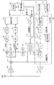
図2は、図1に示すVCO25の第1の構成例を示す回路図である。図2に示すVCO25は、電流源CSと、PチャネルMOS電界効果トランジスターQP10及びQP20と、NチャネルMOS電界効果トランジスターQN10及びQN20とを含んでいる。これらは、ノードN1とノードN2との間に接続されるインダクタンス及び容量に応じた周波数で発振動作を行う発振回路を構成する。
FIG. 2 is a circuit diagram showing a first configuration example of the
また、VCO25は、ノードN1とノードN2との間に接続された少なくとも1つのインダクター(図2においては、2つのインダクターL1及びL2を示す)と、一対の可変容量ダイオード(バリキャップ又はバラクタダイオードともいう)D11及びD21と、もう一対の可変容量ダイオードD12及びD22とを含んでいる。
The
さらに、VCO25は、第1のキャパシターアレイを構成する第1群のキャパシターC11〜C13と、第1群のNチャネルMOS電界効果トランジスターQN11〜QN13と、第1群の抵抗R11〜R13と、第2のキャパシターアレイを構成する第2群のキャパシターC21〜C23と、第2群のNチャネルMOS電界効果トランジスターQN21〜QN23と、第2群の抵抗R21〜R23とを含んでいる。
Further, the
電流源CSは、例えば、PチャネルMOS電界効果トランジスター又は抵抗によって構成され、電源電位VDDに接続された一端を有する。トランジスターQP10は、電流源CSの他端に接続されたソースと、ノードN1に接続されたドレインと、ノードN2に接続されたゲートとを有している。トランジスターQP20は、電流源CSの他端に接続されたソースと、ノードN2に接続されたドレインと、ノードN1に接続されたゲートとを有している。 The current source CS is configured by, for example, a P-channel MOS field effect transistor or a resistor, and has one end connected to the power supply potential VDD. The transistor QP10 has a source connected to the other end of the current source CS, a drain connected to the node N1, and a gate connected to the node N2. Transistor QP20 has a source connected to the other end of current source CS, a drain connected to node N2, and a gate connected to node N1.
トランジスターQN10は、ノードN1に接続されたドレインと、電源電位VSSに接続されたソースと、ノードN2に接続されたゲートとを有している。トランジスターQN20は、ノードN2に接続されたドレインと、電源電位VSSに接続されたソースと、ノードN1に接続されたゲートとを有している。なお、電源電位VDD及びVSSの内の一方を接地電位としても良い。 Transistor QN10 has a drain connected to node N1, a source connected to power supply potential VSS, and a gate connected to node N2. Transistor QN20 has a drain connected to node N2, a source connected to power supply potential VSS, and a gate connected to node N1. Note that one of the power supply potential VDD and VSS may be a ground potential.
可変容量ダイオードD11は、ノードN1に接続されたアノードと、制御電圧VCが印加されるカソードとを有している。また、可変容量ダイオードD21は、ノードN2に接続されたアノードと、制御電圧VCが印加されるカソードとを有している。可変容量ダイオードD11及びD21は、制御電圧VCに従って発振回路の発振周波数を制御することにより、発振信号の周波数を設定する。 The variable capacitance diode D11 has an anode connected to the node N1 and a cathode to which the control voltage VC is applied. The variable capacitance diode D21 has an anode connected to the node N2 and a cathode to which the control voltage VC is applied. The variable capacitance diodes D11 and D21 set the frequency of the oscillation signal by controlling the oscillation frequency of the oscillation circuit according to the control voltage VC.
可変容量ダイオードD12は、ノードN1に接続されたアノードと、変調電圧VMが印加されるカソードとを有している。また、可変容量ダイオードD22は、ノードN2に接続されたアノードと、変調電圧VMが印加されるカソードとを有している。可変容量ダイオードD12及びD22は、変調電圧VMに従って発振回路の発振周波数を制御することにより、発振信号に周波数変調をかける。なお、変調電圧VMを制御電圧VCと共に可変容量ダイオードD11及びD21のカソードに印加することにより、可変容量ダイオードD12及びD22を省略しても良い。 The variable capacitance diode D12 has an anode connected to the node N1 and a cathode to which the modulation voltage VM is applied. The variable capacitance diode D22 has an anode connected to the node N2 and a cathode to which the modulation voltage VM is applied. The variable capacitance diodes D12 and D22 perform frequency modulation on the oscillation signal by controlling the oscillation frequency of the oscillation circuit according to the modulation voltage VM. Note that the variable capacitance diodes D12 and D22 may be omitted by applying the modulation voltage VM together with the control voltage VC to the cathodes of the variable capacitance diodes D11 and D21.
第1のキャパシターアレイを構成する第1群のキャパシターC11〜C13は、ノードN1に接続された第1の端子を有している。第1群のトランジスターQN11〜QN13は、第1群のキャパシターC11〜C13の第2の端子にそれぞれ接続されたドレインと、交流的な接地電位である基準電位(図2においては電源電位VSS)に接続されたソースと、制御信号S11〜S13がそれぞれ供給されるゲートとを有している。トランジスターQN11〜QN13は、制御信号S11〜S13に従ってオン又はオフする。 The first group of capacitors C11 to C13 constituting the first capacitor array has a first terminal connected to the node N1. The first group of transistors QN11 to QN13 are connected to drains respectively connected to the second terminals of the first group of capacitors C11 to C13, and a reference potential (power supply potential VSS in FIG. 2) which is an AC ground potential. It has a connected source and a gate to which control signals S11 to S13 are respectively supplied. Transistors QN11-QN13 are turned on or off in accordance with control signals S11-S13.
また、第2のキャパシターアレイを構成する第2群のキャパシターC21〜C23は、ノードN2に接続された第1の端子を有している。第2群のトランジスターQN21〜QN23は、第2群のキャパシターC21〜C23の第2の端子にそれぞれ接続されたドレインと、基準電位(図2においては電源電位VSS)に接続されたソースと、制御信号S21〜S23がそれぞれ供給されるゲートとを有している。トランジスターQN21〜QN23は、制御信号S21〜S23に従ってオン又はオフする。 The second group of capacitors C21 to C23 constituting the second capacitor array has a first terminal connected to the node N2. The second group of transistors QN21 to QN23 includes a drain connected to the second terminals of the second group of capacitors C21 to C23, a source connected to a reference potential (power supply potential VSS in FIG. 2), and a control. And gates to which signals S21 to S23 are respectively supplied. Transistors QN21-QN23 are turned on or off in accordance with control signals S21-S23.
対応するトランジスターがオンすることによってノードN1又はN2と電源電位VSSとの間に接続されたキャパシターは、インダクターL1及びL2や可変容量ダイオードD11〜D22と共に共振回路を構成する。ノードN1又はN2と電源電位VSSとの間に接続されるキャパシターの数が少ない場合には、VCO25の発振周波数が高くなり、ノードN1又はN2と電源電位VSSとの間に接続されるキャパシターの数が多い場合には、VCO25の発振周波数が低くなる。
The capacitor connected between the node N1 or N2 and the power supply potential VSS when the corresponding transistor is turned on constitutes a resonance circuit together with the inductors L1 and L2 and the variable capacitance diodes D11 to D22. When the number of capacitors connected between the node N1 or N2 and the power supply potential VSS is small, the oscillation frequency of the
図2に示す構成例においては差動増幅型のVCOが用いられているので、第1群のキャパシターC11〜C13の容量値が、第2群のキャパシターC21〜C23の容量値とそれぞれ同一に設定されている。また、第1群のトランジスターQN11〜QN13は、第2群のトランジスターQN21〜QN23とそれぞれ同時にオン/オフするように制御される。 In the configuration example shown in FIG. 2, since the differential amplification type VCO is used, the capacitance values of the first group capacitors C11 to C13 are set to be the same as the capacitance values of the second group capacitors C21 to C23, respectively. Has been. The first group of transistors QN11 to QN13 are controlled to be turned on / off simultaneously with the second group of transistors QN21 to QN23, respectively.
N個のキャパシターC11〜C13(C21〜C23)の容量値が互いに異なる場合には、制御回路40がトランジスターQN11〜QN13(QN21〜QN23)のオン/オフを制御することにより、2N通りの発振周波数を実現することができる。従って、複数の無線通信チャンネルの搬送周波数に対応して、VCO25の発振周波数を補正するキャリブレーションを行うことが可能である。
When the capacitance values of the N capacitors C11 to C13 (C21 to C23) are different from each other, the
例えば、図1に示す制御回路40は、無線通信に先立つキャリブレーションモードにおいて、無線通信において使用される複数の無線通信チャンネルについて、ノードN1又はN2と電源電位VSSとの間に接続されるキャパシターを変化させながらPLL回路20の制御ループ特性を測定することにより、VCO25の発振周波数を補正するためのキャパシターに関する情報を格納部50に格納しておく。
For example, the
また、制御回路40は、実際に無線通信を行う受信モード又は送信モードにおいて、格納部50に格納されている情報を読み出して、その情報に基づいて制御信号S11〜S13及びS21〜S23を生成すると共に、VCO25を含むPLL回路20に電源電圧(VDD−VSS)を供給するように電源回路を制御する。
In addition, the
VCO25に電源電圧が供給されてキャパシターC11〜C13及びC21〜C23の第1の端子における電位が上昇した際に、トランジスターQN11〜QN13及びQN21〜QN23の内のいずれかがオフしていると、オフしているトランジスターのドレイン電位も上昇する。その後、ドレイン電位は下降するが、トランジスターのオフ抵抗は、例えば、10MΩ程度の非常に高い値であるので、トランジスターのオフ抵抗による放電のみでは、ドレイン電位が電源電位VSSに戻るまでに長い期間を要する。
When the power supply voltage is supplied to the
一般に、Nチャネルトランジスターの場合には、N型のドレインとP型の半導体基板又はPウエルとの間に寄生容量(空乏層容量)が存在しており、空乏層容量の容量値は、PN接合に印加される電圧に依存して変化する(谷口研二、宇野重康、「絵から学ぶ半導体デバイス工学」、昭晃堂、P49参照)。なお、P型の半導体基板又はPウエルには、電源電位VSSが供給される。従って、オフしているトランジスターのドレイン電位が下降すると、ドレインと電源電位VSSとの間の寄生容量の値が増加する。 In general, in the case of an N-channel transistor, a parasitic capacitance (depletion layer capacitance) exists between an N-type drain and a P-type semiconductor substrate or P-well, and the capacitance value of the depletion layer capacitance is expressed as a PN junction. The voltage changes depending on the voltage applied to the substrate (see Kenji Taniguchi, Shigeyasu Uno, “Semiconductor Device Engineering Learned from Pictures”, Shosodo, p. 49). Note that the power supply potential VSS is supplied to the P-type semiconductor substrate or the P-well. Therefore, when the drain potential of the transistor that is turned off decreases, the value of the parasitic capacitance between the drain and the power supply potential VSS increases.
その際に、図1に示すスイッチ回路23がオンしていれば、PLL回路20における制御ループによってVCO25の発振周波数が制御されるので、VCO25の発振周波数はドリフトしない。ところが、送信モードにおいて、寄生容量の値が変化している間に、スイッチ回路23がオフしてPLL回路20における制御ループが切断されると、発振信号(搬送波)の周波数がドリフトしてしまう。
At this time, if the
そこで、本実施形態においては、第1群のトランジスターQN11〜QN13にそれぞれ並列に接続された第1群の抵抗R11〜R13と、第2群のトランジスターQN21〜QN23にそれぞれ並列に接続された第2群の抵抗R21〜R23とが設けられている。抵抗R11〜R13及びR21〜R23の抵抗値は、キャパシターの第2の端子に蓄積された電荷を放電する際の時定数を小さくするために、トランジスターのオフ抵抗よりも十分小さい値、例えば100kΩ以下、望ましくは20kΩ以下とする。 Therefore, in the present embodiment, the first group of resistors R11 to R13 connected in parallel to the first group of transistors QN11 to QN13 and the second group of transistors QN21 to QN23 connected in parallel, respectively. Group resistors R21-R23 are provided. The resistance values of the resistors R11 to R13 and R21 to R23 are sufficiently smaller than the off-resistance of the transistor, for example, 100 kΩ or less, in order to reduce the time constant when discharging the charge accumulated in the second terminal of the capacitor. Preferably, it is 20 kΩ or less.
図1に示す制御回路40は、VCO25に電源電圧が供給されてから、キャパシターC11〜C13及びC21〜C23の容量値、及び、対応する抵抗R11〜R13及びR21〜R23の抵抗値によってそれぞれ定まる時定数の最大値以上の期間が経過した後に、スイッチ回路23をオフさせてスイッチ回路72をオンさせる。
The
例えば、キャパシターC11、C12、・・・、C13の容量値の比を、1:2:4:8:・・・としても良い。その場合に、抵抗R11〜R13の抵抗値が同一であれば、キャパシターC13と抵抗R13とによって定まる時定数が最大値となる。従って、制御回路40は、VCO25に電源電圧が供給されてから、キャパシターC13と抵抗R13とによって定まる時定数以上の期間が経過した後に、スイッチ回路23をオフさせてスイッチ回路72をオンさせる。
For example, the ratio of the capacitance values of the capacitors C11, C12,..., C13 may be 1: 2: 4: 8:. In this case, if the resistance values of the resistors R11 to R13 are the same, the time constant determined by the capacitor C13 and the resistor R13 becomes the maximum value. Therefore, the
また、第1群のトランジスターQN11、QN12、・・・、QN13のオン抵抗値の比と、対応するキャパシターC11、C12、・・・、C13の容量値の逆数の比とを略等しくしても良い。例えば、キャパシターC11、C12、・・・、C13の容量値の比が、1:2:4:8:・・・である場合に、トランジスターQN11、QN12、・・・、QN13のオン抵抗値の比を、1:1/2:1/4:1/8:・・・とする。 Further, the ratio of the on-resistance values of the first group of transistors QN11, QN12,..., QN13 and the ratio of the reciprocal of the capacitance values of the corresponding capacitors C11, C12,. good. For example, when the ratio of the capacitance values of the capacitors C11, C12,..., C13 is 1: 2: 4: 8: ..., the ON resistance values of the transistors QN11, QN12,. The ratio is 1: 1/2: 1/4: 1/8:.
同様に、第2群のトランジスターQN21、QN21、・・・、QN23のオン抵抗値の比と、対応するキャパシターC21、C22、・・・、C23の容量値の逆数の比とを略等しくしても良い。例えば、キャパシターC21、C22、・・・、C23の容量値の比が、1:2:4:8:・・・である場合に、トランジスターQN21、QN22、・・・、QN23のオン抵抗値の比を、1:1/2:1/4:1/8:・・・とする。 Similarly, the ratio of the on-resistance values of the second group of transistors QN21, QN21,..., QN23 and the ratio of the reciprocals of the capacitance values of the corresponding capacitors C21, C22,. Also good. For example, when the ratio of the capacitance values of the capacitors C21, C22,..., C23 is 1: 2: 4: 8: ..., the ON resistance values of the transistors QN21, QN22,. The ratio is 1: 1/2: 1/4: 1/8:.
その場合には、トランジスターの駆動能力を、キャパシターの容量値に合わせて設定することができる。トランジスターのオン抵抗値の設定は、例えば、ゲート長を一定にして、ゲート幅を変更することにより行われる。 In that case, the driving capability of the transistor can be set in accordance with the capacitance value of the capacitor. The on-resistance value of the transistor is set, for example, by changing the gate width while keeping the gate length constant.
図3は、図2に示すキャパシターC13の両端電位の経時変化を示す図である。図3(a)は、ノードN1(キャパシターC13の第1の端子)における直流電位の経時変化を示しており、図3(b)は、ノードN3(キャパシターC13の第2の端子)における直流電位の経時変化を示している。また、図3(b)において、破線は、抵抗R13が接続されていない場合を示し、実線は、抵抗R13が接続されている場合を示している。 FIG. 3 is a diagram showing a change with time of the potential at both ends of the capacitor C13 shown in FIG. FIG. 3A shows the change over time of the DC potential at the node N1 (first terminal of the capacitor C13), and FIG. 3B shows the DC potential at the node N3 (second terminal of the capacitor C13). The change with time is shown. In FIG. 3B, a broken line indicates a case where the resistor R13 is not connected, and a solid line indicates a case where the resistor R13 is connected.
時刻t0においてVCO25に電源電圧が供給されると、図3(a)に示すように、ノードN1の電位が上昇する。また、トランジスターQN13がオフしていると、図3(b)に示すように、ノードN3の電位も上昇する。図3(b)に破線で示すように、抵抗R13が接続されていない場合には、ノードN3の電位が電源電位VSSに戻るまでに長い期間を要する。一方、図3(b)に実線で示すように、抵抗R13が接続されている場合には、ノードN3の電位が電源電位VSSに戻るまでに要する期間が短縮される。
When the power supply voltage is supplied to the
図1に示す制御回路40は、VCO25に電源電圧が供給されてから、キャパシターC13と抵抗R13とによって定まる時定数以上の期間が経過して、VCO25の発振周波数が所定の周波数の近くにロックされた時刻t1において、スイッチ回路23をオフさせる。時刻t1においては、ノードN3の電位が電源電位VSSに十分近付いているので、スイッチ回路23をオフさせても、VCO25における搬送周波数のドリフトは狭い範囲内に抑えられる。
In the
あるいは、制御回路40は、VCO25に電源電圧が供給されてから、トランジスターQN11〜QN13及びQN21〜QN23を一旦オンさせて、キャパシターC11〜C13及びC21〜C23の第2の端子の電荷を放電させても良い。さらに、制御回路40は、トランジスターQN11〜QN13及びQN21〜QN23の内の所定のトランジスターをオフさせてVCO25の発振周波数がロックされた後に、スイッチ回路23をオフさせてスイッチ回路72をオンさせるようにしても良い。その場合には、図2に示す抵抗R11〜R13及びR21〜R23を省略することができる。
Alternatively, after the power supply voltage is supplied to the
ここで、VCO25の発振周波数がロックされたか否かは、PLL回路20に電源電圧が供給されてから経過した時間に基づいて制御回路40が判断しても良いし、ロック検出回路30が判断しても良い。ロック検出回路30は、発振回路10から出力される基準信号と、PLL回路20から出力される分周信号とを比較することにより、それらの位相差に基づいて、PLL回路がロックしているか否かを検出する。例えば、ロック検出回路30は、基準信号と分周信号との位相差が所定の期間に亘って所定値以下である場合に、PLL回路20がロックしたことを検出する。
Here, whether or not the oscillation frequency of the
図4は、図1に示すVCO25の第2の構成例を示す回路図である。電流源CS及びトランジスターQP10、QP20、QN10、QN20によって構成される発振回路と、インダクターL1及びL2と、可変容量ダイオードD11〜D22とに関する接続は、図2に示す第1の構成例におけるのと同様である。なお、第2の構成例においては、電源電位VSSを接地電位としている。
FIG. 4 is a circuit diagram showing a second configuration example of the
さらに、VCO25は、第1のキャパシターアレイを構成する第1群のキャパシターC11〜C13と、第2のキャパシターアレイを構成する第2群のキャパシターC21〜C23と、複数のNチャネルMOS電界効果トランジスターQN1〜QN3と、第1群の抵抗R11〜R13と、第2群の抵抗R21〜R23とを含んでいる。
Further, the
第1のキャパシターアレイを構成する第1群のキャパシターC11〜C13は、ノードN1に接続された第1の端子を有している。また、第2のキャパシターアレイを構成する第2群のキャパシターC21〜C23は、ノードN2に接続された第1の端子を有している。 The first group of capacitors C11 to C13 constituting the first capacitor array has a first terminal connected to the node N1. The second group of capacitors C21 to C23 constituting the second capacitor array has a first terminal connected to the node N2.
複数のトランジスターQN1〜QN3は、第1群のキャパシターC11〜C13の第2の端子にそれぞれ接続されたドレイン又はソースと、第2群のキャパシターC21〜C23の第2の端子にそれぞれ接続されたソース又はドレインと、制御信号S1〜S3がそれぞれ供給されるゲートとを有している。トランジスターQN1〜QN3は、制御信号S1〜S3に従ってオン又はオフする。 The plurality of transistors QN1 to QN3 are drains or sources connected to the second terminals of the first group of capacitors C11 to C13, respectively, and sources connected to the second terminals of the second group of capacitors C21 to C23, respectively. Alternatively, it has a drain and a gate to which control signals S1 to S3 are respectively supplied. The transistors QN1 to QN3 are turned on or off according to the control signals S1 to S3.
対応するトランジスターがオンすることによってノードN1とノードN2との間に接続されたキャパシターは、インダクターL1及びL2や可変容量ダイオードD11〜D22と共に共振回路を構成する。ノードN1とノードN2との間に接続されるキャパシターの数が少ない場合には、VCO25の発振周波数が高くなり、ノードN1とノードN2との間に接続されるキャパシターの数が多い場合には、VCO25の発振周波数が低くなる。
The capacitor connected between the node N1 and the node N2 by turning on the corresponding transistor forms a resonance circuit together with the inductors L1 and L2 and the variable capacitance diodes D11 to D22. When the number of capacitors connected between the node N1 and the node N2 is small, the oscillation frequency of the
図4に示す構成例においては差動増幅型のVCOが用いられているので、第1群のキャパシターC11〜C13の容量値が、第2群のキャパシターC21〜C23の容量値とそれぞれ同一に設定されている。 In the configuration example shown in FIG. 4, since the differential amplification type VCO is used, the capacitance values of the first group capacitors C11 to C13 are set to be the same as the capacitance values of the second group capacitors C21 to C23, respectively. Has been.
ここで、トランジスターQN1〜QN3のドレイン及びソースをフローティングとしておくと、オン又はオフの動作を確実に行うことができないおそれがある。そこで、本実施形態においては、第1群のキャパシターC11〜C13の第2の端子(トランジスターQN1〜QN3のドレイン又はソース)と基準電位(図4においては電源電位VSS)との間にそれぞれ接続された第1群の抵抗R11〜R13を設けている。 Here, if the drains and sources of the transistors QN1 to QN3 are left floating, there is a possibility that the on / off operation cannot be performed reliably. Therefore, in the present embodiment, the second terminals of the first group of capacitors C11 to C13 (the drains or sources of the transistors QN1 to QN3) and the reference potential (the power supply potential VSS in FIG. 4) are respectively connected. The first group of resistors R11 to R13 are provided.
さらに、トランジスターQN1〜QN3の内のいずれかがオフしたときに、オフしたトランジスターにリーク電流が流れないように、好ましくは第1群の抵抗R11〜R13の抵抗値と同じ抵抗値をそれぞれ有する第2群の抵抗R21〜R23が、第2群のキャパシターC21〜C23の第2の端子(トランジスターQN1〜QN3のソース又はドレイン)と基準電位との間にそれぞれ接続されている。 Further, when any of the transistors QN1 to QN3 is turned off, the first resistances preferably have the same resistance values as the resistance values of the first group of resistors R11 to R13 so that no leak current flows through the turned off transistors. Two groups of resistors R21 to R23 are connected between the second terminals of the second group of capacitors C21 to C23 (the sources or drains of the transistors QN1 to QN3) and the reference potential, respectively.
抵抗R11〜R13及びR21〜R23の抵抗値は、キャパシターの第2の端子に蓄積された電荷を放電する際の時定数を小さくするために、例えば100kΩ以下、望ましくは20kΩ以下とする。 The resistance values of the resistors R11 to R13 and R21 to R23 are, for example, 100 kΩ or less, preferably 20 kΩ or less, in order to reduce the time constant when discharging the charge accumulated in the second terminal of the capacitor.
VCO25に電源電圧が供給されてキャパシターC11〜C13及びC21〜C23の第1の端子における電位が上昇した際に、トランジスターQN1〜QN3のドレイン電位及びソース電位も上昇する。その後、ドレイン電位及びソース電位は下降するが、それに伴って、ドレインと電源電位VSSとの間の寄生容量及びソースと電源電位VSSとの間の寄生容量の値が増加する。
When the power supply voltage is supplied to the
その際に、図1に示すスイッチ回路23がオンしていれば、PLL回路20における制御ループによってVCO25の発振周波数が制御されるので、VCO25の発振周波数はドリフトしない。ところが、送信モードにおいて、寄生容量の値が変化している間に、図1に示すスイッチ回路23がオフしてPLL回路20における制御ループが切断されると、発振信号(搬送波)の周波数がドリフトしてしまう。
At this time, if the
そこで、図1に示す制御回路40は、VCO25に電源電圧が供給されてから、キャパシターC11〜C13及びC21〜C23の容量値、及び、対応する抵抗R11〜R13及びR21〜R23の抵抗値によってそれぞれ定まる時定数の最大値以上の期間が経過した後に、スイッチ回路23をオフさせてスイッチ回路72をオンさせる。
Therefore, after the power supply voltage is supplied to the
例えば、キャパシターC11、C12、・・・、C13の容量値の比を、1:2:4:8:・・・としても良い。その場合に、抵抗R11〜R13の抵抗値が同一であれば、キャパシターC13と抵抗R13とによって定まる時定数が最大値となる。従って、制御回路40は、VCO25に電源電圧が供給されてから、キャパシターC13と抵抗R13とによって定まる時定数以上の期間が経過して、VCO25の発振周波数が所定の周波数の近くにロックされた後に、スイッチ回路23をオフさせてスイッチ回路72をオンさせる。
For example, the ratio of the capacitance values of the capacitors C11, C12,..., C13 may be 1: 2: 4: 8:. In this case, if the resistance values of the resistors R11 to R13 are the same, the time constant determined by the capacitor C13 and the resistor R13 becomes the maximum value. Therefore, the
また、トランジスターQN1、QN2、・・・、QN3のオン抵抗値の比と、第1のキャパシターアレイにおいて対応する第1群のキャパシターC11、C12、・・・、C13の容量値の逆数の比と、第2のキャパシターアレイにおいて対応する第2群のキャパシターC21、C22、・・・、C23の容量値の逆数の比とを略等しくしても良い。 Further, the ratio of the on-resistance values of the transistors QN1, QN2,..., QN3 and the ratio of the reciprocal of the capacitance values of the first group capacitors C11, C12,. The ratio of the reciprocals of the capacitance values of the second group of capacitors C21, C22,..., C23 corresponding to the second capacitor array may be substantially equal.
例えば、キャパシターC11、C12、・・・、C13の容量値の比、及び、キャパシターC21、C22、・・・、C23の容量値の比が、1:2:4:8:・・・である場合に、トランジスターQN1、QN2、・・・、QN3のオン抵抗値の比を、1:1/2:1/4:1/8:・・・とする。その場合には、トランジスターの駆動能力を、キャパシターの容量値に合わせて設定することができる。 For example, the ratio of the capacitance values of the capacitors C11, C12,..., C13 and the ratio of the capacitance values of the capacitors C21, C22,..., C23 are 1: 2: 4: 8:. In this case, the ratio of the on-resistance values of the transistors QN1, QN2,..., QN3 is 1: 1/2: 1/4: 1/8:. In that case, the driving capability of the transistor can be set in accordance with the capacitance value of the capacitor.
以上の実施形態においては、MOSFETを用いる場合について説明したが、その他の電界効果トランジスターやバイポーラトランジスターを用いても良い。バイポーラトランジスターを用いる場合には、バイポーラトランジスターのベース、エミッター、コレクターが、電界効果トランジスターのゲート、ソース、ドレインに相当する。また、本発明は、以上説明した実施形態に限定されるものではなく、当該技術分野において通常の知識を有する者によって、本発明の技術的思想内で多くの変形が可能である。 In the above embodiment, the case of using the MOSFET has been described, but other field effect transistors and bipolar transistors may be used. When a bipolar transistor is used, the base, emitter, and collector of the bipolar transistor correspond to the gate, source, and drain of the field effect transistor. The present invention is not limited to the embodiments described above, and many modifications can be made within the technical idea of the present invention by those who have ordinary knowledge in the technical field.
10…発振回路、20…PLL回路、21…位相比較回路、22…チャージポンプ、23…スイッチ回路、24…ループフィルター、25…VCO、26…分周回路、30…ロック検出回路、40…制御回路、50…格納部、60…ローノイズアンプ、61〜63…ミキサー、64…分周回路、65…位相シフト回路、66…バンドパスフィルター、67…リミッター、68…復調回路、70…パワーアンプ、71…DAC、72…スイッチ回路、73…ガウシアンフィルター、CS…電流源、QP10、QP20…PチャネルMOS電界効果トランジスター、QN1〜QN23…NチャネルMOS電界効果トランジスター、L1、L2…インダクター、D11〜D22…可変容量ダイオード、C11〜C23…キャパシター、R11〜R23…抵抗。
DESCRIPTION OF
Claims (6)
前記電圧制御発振器によって生成される発振信号を分周して分周信号を出力する分周回路と、
前記分周回路から出力される分周信号の少なくとも位相と基準信号の少なくとも位相とを比較することにより、それらの差に応じた誤差信号を生成する誤差信号生成回路と、
前記誤差信号にローパスフィルター処理を施すことにより、前記電圧制御発振器の発振周波数を制御するための制御電圧を生成する第1のフィルター回路と、
前記第1のフィルター回路への前記誤差信号の供給をオン又はオフする第1のスイッチ回路と、
変調信号にローパスフィルター処理を施すことにより、前記電圧制御発振器の発振周波数を制御するための制御電圧を生成する第2のフィルター回路と、
前記第2のフィルター回路への変調信号の供給をオン又はオフする第2のスイッチ回路と、
前記第1のスイッチ回路及び前記第2のスイッチ回路を制御する制御回路と、
を具備し、
前記制御回路は、前記電圧制御発振器に電源電圧が供給されてから、前記第1群及び第2群のキャパシターの容量値及び対応する前記第1群及び第2群の抵抗の抵抗値によってそれぞれ定まる時定数の最大値以上の期間が経過した後に、前記第1のスイッチ回路をオフさせて前記第2のスイッチ回路をオンさせる、
信号発生装置。 An oscillation circuit that oscillates at a frequency corresponding to an inductance and a capacitance connected between the first node and the second node, and a first group having a first terminal connected to the first node And a first group of transistors connected between a second terminal of the first group of capacitors and a reference potential, and turned on or off according to respective control signals, and a first group of transistors, respectively. A first group of resistors connected in parallel; a second group of capacitors having a first terminal connected to the second node; a second terminal of the second group of capacitors; and the reference potential. And a second group of transistors connected in parallel to each of the second group of transistors, each of which is connected between the first group of transistors and is turned on or off according to a respective control signal. And a voltage controlled oscillator, including,
A frequency divider that divides the oscillation signal generated by the voltage controlled oscillator and outputs a frequency-divided signal;
An error signal generation circuit that generates an error signal according to a difference between at least a phase of the frequency-divided signal output from the frequency-dividing circuit and at least a phase of the reference signal;
A first filter circuit that generates a control voltage for controlling an oscillation frequency of the voltage controlled oscillator by performing low-pass filtering on the error signal;
A first switch circuit for turning on or off the supply of the error signal to the first filter circuit;
A second filter circuit that generates a control voltage for controlling the oscillation frequency of the voltage controlled oscillator by performing low-pass filtering on the modulation signal;
A second switch circuit for turning on or off the supply of the modulation signal to the second filter circuit;
A control circuit for controlling the first switch circuit and the second switch circuit;
Equipped with,
The control circuit is determined by the capacitance values of the capacitors of the first group and the second group and the corresponding resistance values of the resistors of the first group and the second group after the power supply voltage is supplied to the voltage controlled oscillator. After a period equal to or greater than the maximum value of the time constant has elapsed, the first switch circuit is turned off to turn on the second switch circuit;
Signal generator.
前記電圧制御発振器によって生成される発振信号を分周して分周信号を出力する分周回路と、
前記分周回路から出力される分周信号の少なくとも位相と基準信号の少なくとも位相とを比較することにより、それらの差に応じた誤差信号を生成する誤差信号生成回路と、
前記誤差信号にローパスフィルター処理を施すことにより、前記電圧制御発振器の発振周波数を制御するための制御電圧を生成する第1のフィルター回路と、
前記第1のフィルター回路への前記誤差信号の供給をオン又はオフする第1のスイッチ回路と、
変調信号にローパスフィルター処理を施すことにより、前記電圧制御発振器の発振周波数を制御するための制御電圧を生成する第2のフィルター回路と、
前記第2のフィルター回路への変調信号の供給をオン又はオフする第2のスイッチ回路と、
前記第1のスイッチ回路及び前記第2のスイッチ回路を制御する制御回路と、
を具備し、
前記制御回路は、前記電圧制御発振器に電源電圧が供給されてから、前記第1群及び第2群のトランジスターを一旦オンさせて前記第1群及び第2群のキャパシターの第2の端子の電荷を放電させ、前記第1群及び第2群のトランジスターの内の所定のトランジスターをオフさせて前記電圧制御発振器の発振周波数がロックされた後に、前記第1のスイッチ回路をオフさせて前記第2のスイッチ回路をオンさせる、
信号発生装置。 An oscillation circuit that oscillates at a frequency corresponding to an inductance and a capacitance connected between the first node and the second node, and a first group having a first terminal connected to the first node And a first group of transistors connected between a second terminal of the first group of capacitors and a reference potential, and turned on or off according to respective control signals, and a first group of transistors, respectively. A first group of resistors connected in parallel; a second group of capacitors having a first terminal connected to the second node; a second terminal of the second group of capacitors; and the reference potential. And a second group of transistors connected in parallel to each of the second group of transistors, each of which is connected between the first group of transistors and is turned on or off according to a respective control signal. And a voltage controlled oscillator, including,
A frequency divider that divides the oscillation signal generated by the voltage controlled oscillator and outputs a frequency-divided signal;
An error signal generation circuit that generates an error signal according to a difference between at least a phase of the frequency-divided signal output from the frequency-dividing circuit and at least a phase of the reference signal;
A first filter circuit that generates a control voltage for controlling an oscillation frequency of the voltage controlled oscillator by performing low-pass filtering on the error signal;
A first switch circuit for turning on or off the supply of the error signal to the first filter circuit;
A second filter circuit that generates a control voltage for controlling the oscillation frequency of the voltage controlled oscillator by performing low-pass filtering on the modulation signal;
A second switch circuit for turning on or off the supply of the modulation signal to the second filter circuit;
A control circuit for controlling the first switch circuit and the second switch circuit;
Equipped with,
The control circuit temporarily turns on the first group and second group transistors after the power supply voltage is supplied to the voltage controlled oscillator, and charges the second terminals of the first group and second group capacitors. Is discharged, a predetermined transistor in the first group and the second group of transistors is turned off to lock the oscillation frequency of the voltage controlled oscillator, and then the first switch circuit is turned off to turn off the second switch. Turn on the switch circuit,
Signal generator.
前記第1のノードに接続された第1の端子を有する第1のキャパシターと、
前記第1のキャパシターの第2の端子と基準電位との間に接続され、制御信号に従ってオン又はオフする第1のトランジスターと、
前記第1のトランジスターと並列に接続された第1の抵抗と、
前記第2のノードに接続された第1の端子を有する第2のキャパシターと、
前記第2のキャパシターの第2の端子と前記基準電位との間に接続され、制御信号に従ってオン又はオフする第2のトランジスターと、
前記第2のトランジスターと並列に接続された第2の抵抗と、
を具備する電圧制御発振器と、
前記電圧制御発振器によって生成される発振信号を分周して分周信号を出力する分周回路と、
前記分周回路から出力される分周信号の少なくとも位相と基準信号の少なくとも位相とを比較することにより、それらの差に応じた誤差信号を生成する誤差信号生成回路と、
前記誤差信号にローパスフィルター処理を施すことにより、前記電圧制御発振器の発振周波数を制御するための制御電圧を生成するフィルター回路と、
前記フィルター回路への前記誤差信号の供給をオン又はオフするスイッチ回路と、
前記スイッチ回路を制御する制御回路と、
を含み、
前記第1のキャパシターの容量値と前記第1の抵抗の抵抗値により定まる時定数を第1の時定数とし、前記第2のキャパシターの容量値と前記第2の抵抗の抵抗値により定まる時定数を第2の時定数とした場合に、前記制御回路は、前記第1の時定数と前記第2の時定数の最大値以上の期間が前記電圧制御発振器に電源電圧が供給されてから経過した後に、前記スイッチ回路をオフさせる、
信号発生装置。 An oscillation circuit that oscillates at a frequency corresponding to an inductance and a capacitance connected between the first node and the second node;
A first capacitor having a first terminal connected to the first node;
A first transistor connected between a second terminal of the first capacitor and a reference potential and turned on or off according to a control signal;
A first resistor connected in parallel with the first transistor;
A second capacitor having a first terminal connected to the second node;
A second transistor connected between a second terminal of the second capacitor and the reference potential and turned on or off according to a control signal;
A second resistor connected in parallel with the second transistor;
A voltage controlled oscillator comprising:
A frequency divider that divides the oscillation signal generated by the voltage controlled oscillator and outputs a frequency-divided signal;
An error signal generation circuit that generates an error signal according to a difference between at least a phase of the frequency-divided signal output from the frequency-dividing circuit and at least a phase of the reference signal;
A filter circuit that generates a control voltage for controlling the oscillation frequency of the voltage controlled oscillator by performing low-pass filtering on the error signal;
A switch circuit for turning on or off the supply of the error signal to the filter circuit;
A control circuit for controlling the switch circuit;
Only including,
A time constant determined by the capacitance value of the first capacitor and the resistance value of the first resistor is defined as a first time constant, and the time constant determined by the capacitance value of the second capacitor and the resistance value of the second resistor. Is set to the second time constant, the control circuit has passed a period longer than the maximum value of the first time constant and the second time constant after the power supply voltage is supplied to the voltage controlled oscillator. Later, the switch circuit is turned off,
Signal generator.
前記第1のノードに接続された第1の端子を有する第1のキャパシターと、
前記第2のノードに接続された第1の端子を有する第2のキャパシターと、
前記第1のキャパシターの第2の端子と前記第2のキャパシターの第2の端子との間に接続され、制御信号に従ってオン又はオフするトランジスターと、
前記第1のキャパシターの第2の端子と基準電位との間に接続された第1の抵抗と、
前記第2のキャパシターの第2の端子と前記基準電位との間に接続された第2の抵抗と、
を具備する電圧制御発振器と、
前記電圧制御発振器によって生成される発振信号を分周して分周信号を出力する分周回路と、
前記分周回路から出力される分周信号の少なくとも位相と基準信号の少なくとも位相とを比較することにより、それらの差に応じた誤差信号を生成する誤差信号生成回路と、
前記誤差信号生成回路によって生成される前記誤差信号にローパスフィルター処理を施すことにより、前記電圧制御発振器の発振周波数を制御するための制御電圧を生成するフィルター回路と、
前記フィルター回路への前記誤差信号の供給をオン又はオフするスイッチ回路と、
前記スイッチ回路を制御する制御回路と、
を含み、
前記第1のキャパシターの容量値と前記第1の抵抗の抵抗値により定まる時定数を第1の時定数とし、前記第2のキャパシターの容量値と前記第2の抵抗の抵抗値により定まる時定数を第2の時定数とした場合に、前記制御回路は、前記第1の時定数と前記第2の時定数の最大値以上の期間が前記電圧制御発振器に電源電圧が供給されてから経過した後に、前記スイッチ回路をオフさせる、
信号発生装置。 An oscillation circuit that oscillates at a frequency corresponding to an inductance and a capacitance connected between the first node and the second node;
A first capacitor having a first terminal connected to the first node;
A second capacitor having a first terminal connected to the second node;
A transistor connected between a second terminal of the first capacitor and a second terminal of the second capacitor and turned on or off according to a control signal;
A first resistor connected between a second terminal of the first capacitor and a reference potential;
A second resistor connected between a second terminal of the second capacitor and the reference potential;
A voltage controlled oscillator comprising:
A frequency divider that divides the oscillation signal generated by the voltage controlled oscillator and outputs a frequency-divided signal;
An error signal generation circuit that generates an error signal according to a difference between at least a phase of the frequency-divided signal output from the frequency-dividing circuit and at least a phase of the reference signal;
A filter circuit that generates a control voltage for controlling an oscillation frequency of the voltage controlled oscillator by performing a low-pass filter process on the error signal generated by the error signal generation circuit;
A switch circuit for turning on or off the supply of the error signal to the filter circuit;
A control circuit for controlling the switch circuit;
Only including,
A time constant determined by the capacitance value of the first capacitor and the resistance value of the first resistor is defined as a first time constant, and the time constant determined by the capacitance value of the second capacitor and the resistance value of the second resistor. Is set to the second time constant, the control circuit has passed a period longer than the maximum value of the first time constant and the second time constant after the power supply voltage is supplied to the voltage controlled oscillator. Later, the switch circuit is turned off,
Signal generator.
前記第1のノードに接続された第1の端子を有する第1のキャパシターと、
前記第1のキャパシターの第2の端子と基準電位との間に接続された第1の抵抗と、
前記第1のキャパシターの第2の端子に接続されるソース端子又はドレイン端子を有するトランジスターと、
を具備する電圧制御発振器と、
前記電圧制御発振器によって生成される発振信号を分周して分周信号を出力する分周回路と、
前記分周回路から出力される分周信号の少なくとも位相と基準信号の少なくとも位相とを比較することにより、それらの差に応じた誤差信号を生成する誤差信号生成回路と、
前記誤差信号生成回路によって生成される前記誤差信号にローパスフィルター処理を施すことにより、前記電圧制御発振器の発振周波数を制御するための制御電圧を生成するフィルター回路と、
前記フィルター回路への前記誤差信号の供給をオン又はオフするスイッチ回路と、
前記スイッチ回路を制御する制御回路と、
を含み、
前記第1のキャパシターの容量値と前記第1の抵抗の抵抗値により定まる時定数を第1の時定数とした場合に、前記制御回路は、前記電圧制御発振器に電源電圧が供給されてから前記第1の時定数以上の期間が経過した後に、前記スイッチ回路をオフさせる、
信号発生装置。 An oscillation circuit that oscillates at a frequency corresponding to an inductance and a capacitance connected between the first node and the second node;
A first capacitor having a first terminal connected to the first node;
A first resistor connected between a second terminal of the first capacitor and a reference potential;
A transistor having a source terminal or a drain terminal connected to a second terminal of the first capacitor;
A voltage controlled oscillator comprising:
A frequency divider that divides the oscillation signal generated by the voltage controlled oscillator and outputs a frequency-divided signal;
An error signal generation circuit that generates an error signal according to a difference between at least a phase of the frequency-divided signal output from the frequency-dividing circuit and at least a phase of the reference signal;
A filter circuit that generates a control voltage for controlling an oscillation frequency of the voltage controlled oscillator by performing a low-pass filter process on the error signal generated by the error signal generation circuit;
A switch circuit for turning on or off the supply of the error signal to the filter circuit;
A control circuit for controlling the switch circuit;
Only including,
In the case where the time constant determined by the capacitance value of the first capacitor and the resistance value of the first resistor is the first time constant, the control circuit is configured to supply the power supply voltage to the voltage controlled oscillator after the power supply voltage is supplied. Turning off the switch circuit after a period of time equal to or greater than the first time constant has elapsed;
Signal generator.
Applications Claiming Priority (3)
| Application Number | Priority Date | Filing Date | Title |
|---|---|---|---|
| JP2012054176 | 2012-03-12 | ||
| JP2012054176 | 2012-03-12 | ||
| PCT/JP2013/001580 WO2013136766A1 (en) | 2012-03-12 | 2013-03-11 | Voltage controlled oscillator, signal generating apparatus, and electronic apparatus |
Publications (2)
| Publication Number | Publication Date |
|---|---|
| JPWO2013136766A1 JPWO2013136766A1 (en) | 2015-08-03 |
| JP6206397B2 true JP6206397B2 (en) | 2017-10-04 |
Family
ID=49160697
Family Applications (1)
| Application Number | Title | Priority Date | Filing Date |
|---|---|---|---|
| JP2014504693A Active JP6206397B2 (en) | 2012-03-12 | 2013-03-11 | Signal generator and electronic device |
Country Status (4)
| Country | Link |
|---|---|
| US (1) | US9236872B2 (en) |
| JP (1) | JP6206397B2 (en) |
| CN (1) | CN104160627B (en) |
| WO (1) | WO2013136766A1 (en) |
Families Citing this family (17)
| Publication number | Priority date | Publication date | Assignee | Title |
|---|---|---|---|---|
| US20160079945A1 (en) * | 2014-09-16 | 2016-03-17 | Texas Instruments Incorporated | Programmable impedance network in an amplifier |
| JP6691287B2 (en) * | 2015-11-18 | 2020-04-28 | 株式会社ソシオネクスト | Voltage controlled oscillator circuit and PLL circuit |
| US9906230B2 (en) * | 2016-04-14 | 2018-02-27 | Huawei Technologies Co., Ltd. | PLL system and method of operating same |
| JP6524981B2 (en) * | 2016-07-29 | 2019-06-05 | 株式会社デンソー | Ringing suppression circuit |
| CN108270469B (en) * | 2016-12-30 | 2023-06-30 | 丰郅(上海)新能源科技有限公司 | Electronic device capable of realizing near field wireless communication and self-checking method of oscillation circuit of electronic device |
| US10381981B2 (en) * | 2017-09-15 | 2019-08-13 | Qualcomm Incorporated | Degeneration for a wideband voltage-controlled oscillator |
| US10447204B2 (en) | 2017-09-15 | 2019-10-15 | Qualcomm Incorporated | Switchable inductor network for wideband circuits |
| CN111264034A (en) * | 2017-10-25 | 2020-06-09 | 日本精机株式会社 | Receiving circuit and communication device |
| KR102581650B1 (en) * | 2018-06-28 | 2023-09-25 | 삼성전자주식회사 | Discrete capacitance switching circuit and capacitor array circuit including the same |
| US11948945B2 (en) | 2019-05-31 | 2024-04-02 | Semiconductor Energy Laboratory Co., Ltd. | Semiconductor device and wireless communication device with the semiconductor device |
| JP7367350B2 (en) * | 2019-06-21 | 2023-10-24 | セイコーエプソン株式会社 | Circuit devices, oscillators, electronic equipment and mobile objects |
| CN113037219B (en) * | 2019-12-24 | 2025-02-11 | 炬芯科技股份有限公司 | A crystal oscillator control circuit, a crystal oscillator start-up control method and an electronic device |
| CN111817668B (en) * | 2020-09-02 | 2020-12-18 | 深圳市汇顶科技股份有限公司 | Capacitor array circuit, charging and discharging circuit and RC oscillation circuit |
| CN112737576B (en) * | 2020-12-16 | 2023-12-12 | 深圳市紫光同创电子有限公司 | Frequency selection circuit |
| KR102321030B1 (en) * | 2021-04-08 | 2021-11-03 | 주식회사 스카이칩스 | Signal synthesizer, signal synthesis method and communication apparatus adjusting automatically frequency deviation difference according to the two point modulation of the phase lock loop |
| CN114400991A (en) * | 2021-12-20 | 2022-04-26 | 普源精电科技股份有限公司 | Adjustable capacitance circuit and time delay adjusting circuit |
| CN115529006B (en) * | 2022-11-25 | 2023-03-10 | 成都爱旗科技有限公司 | Frequency band switching circuit, frequency band switching method and voltage-controlled oscillator |
Family Cites Families (19)
| Publication number | Priority date | Publication date | Assignee | Title |
|---|---|---|---|---|
| JPS60145720U (en) * | 1984-03-09 | 1985-09-27 | 日本電信電話株式会社 | Digitally controlled piezoelectric oscillator circuit |
| JPH06291653A (en) * | 1993-04-02 | 1994-10-18 | Fujitsu Ltd | Modulator using PLL |
| US6013958A (en) * | 1998-07-23 | 2000-01-11 | Lucent Technologies Inc. | Integrated circuit with variable capacitor |
| US6876266B2 (en) * | 2002-06-10 | 2005-04-05 | Gct Semiconductor, Inc. | LC oscillator with wide tuning range and low phase noise |
| JP2004289339A (en) * | 2003-03-20 | 2004-10-14 | Alps Electric Co Ltd | Multi-band oscillator |
| TW200520121A (en) | 2003-08-28 | 2005-06-16 | Gct Semiconductor Inc | Integrated circuit package having an inductance loop formed from a multi-loop configuration |
| US7116183B2 (en) * | 2004-02-05 | 2006-10-03 | Qualcomm Incorporated | Temperature compensated voltage controlled oscillator |
| JP4471849B2 (en) * | 2004-03-31 | 2010-06-02 | Necエレクトロニクス株式会社 | PLL frequency synthesizer circuit and frequency tuning method thereof |
| EP1583221A1 (en) * | 2004-03-31 | 2005-10-05 | NEC Compound Semiconductor Devices, Ltd. | PLL frequency synthesizer circuit and frequency tuning method thereof |
| US7209017B2 (en) * | 2004-08-04 | 2007-04-24 | Via Technologies, Inc. | Symmetrical linear voltage controlled oscillator |
| JP2006060395A (en) | 2004-08-18 | 2006-03-02 | Toshiba Corp | Voltage controlled oscillator |
| JP2006216763A (en) * | 2005-02-03 | 2006-08-17 | Toshiba Corp | Capacitor array circuit and voltage controlled oscillator |
| JP2007006307A (en) * | 2005-06-27 | 2007-01-11 | Oki Electric Ind Co Ltd | Radio unit |
| JP4676894B2 (en) * | 2006-01-31 | 2011-04-27 | 富士通株式会社 | Resonator type oscillator and tuning capacitor circuit |
| JP2010056856A (en) * | 2008-08-28 | 2010-03-11 | Renesas Technology Corp | Semiconductor integrated circuit |
| JP2010278491A (en) * | 2009-05-26 | 2010-12-09 | Renesas Electronics Corp | Frequency synthesizer |
| JP2011109163A (en) * | 2009-11-12 | 2011-06-02 | Seiko Epson Corp | Radio circuit, integrated circuit device and electronic apparatus |
| JP2011109162A (en) * | 2009-11-12 | 2011-06-02 | Seiko Epson Corp | Transmission circuit, integrated circuit device, and electronic equipment |
| JP5174055B2 (en) * | 2010-02-02 | 2013-04-03 | 株式会社半導体理工学研究センター | Broadband oscillator circuit |
-
2013
- 2013-03-11 WO PCT/JP2013/001580 patent/WO2013136766A1/en not_active Ceased
- 2013-03-11 US US14/384,248 patent/US9236872B2/en active Active
- 2013-03-11 CN CN201380014143.1A patent/CN104160627B/en active Active
- 2013-03-11 JP JP2014504693A patent/JP6206397B2/en active Active
Also Published As
| Publication number | Publication date |
|---|---|
| JPWO2013136766A1 (en) | 2015-08-03 |
| US9236872B2 (en) | 2016-01-12 |
| US20150077193A1 (en) | 2015-03-19 |
| CN104160627A (en) | 2014-11-19 |
| WO2013136766A1 (en) | 2013-09-19 |
| CN104160627B (en) | 2017-05-17 |
Similar Documents
| Publication | Publication Date | Title |
|---|---|---|
| JP6206397B2 (en) | Signal generator and electronic device | |
| US9344100B2 (en) | Reconfigurable local oscillator for optimal noise performance in a multi-standard transceiver | |
| JP4089938B2 (en) | Voltage controlled oscillator | |
| US8067995B2 (en) | Voltage controlled oscillator, and PLL circuit and wireless communication device each using the same | |
| US20030227341A1 (en) | Voltage-controlled oscillator and frequency synthesizer | |
| US20090231044A1 (en) | Voltage controlled oscillator having temperature detecting circuit | |
| US10516404B2 (en) | Voltage controlled oscillator using variable capacitor and phase locked loop using the same | |
| US20070262825A1 (en) | Embedded structure circuit for VCO and regulator | |
| US20090108947A1 (en) | Voltage Controlled Oscillator | |
| US7847646B2 (en) | Carrier generator with LC network | |
| US8222963B2 (en) | Voltage-controlled oscillator | |
| US7701304B2 (en) | Voltage controlled oscillator, and PLL circuit and radio communication apparatus using the same | |
| US9673755B1 (en) | Controlling a switched capacitor bank in a voltage controlled oscillator for wireless sensor devices | |
| US9602051B1 (en) | Transforming voltage in a voltage controlled oscillator for wireless sensor devices | |
| US7421052B2 (en) | Oscillator frequency selection | |
| US7944318B2 (en) | Voltage controlled oscillator, and PLL circuit and radio communication device each including the same | |
| US7012487B2 (en) | Transconductance device employing native MOS transistors | |
| US7750692B2 (en) | Digital divider for low voltage LOGEN | |
| CN101263653B (en) | Analog varactor | |
| JP2006216763A (en) | Capacitor array circuit and voltage controlled oscillator | |
| US6995625B2 (en) | Oscillator with quadrature output in a cross-coupled configuration | |
| Jahan et al. | A 167 μW 915 MHz gain-boosted LC VCO | |
| Shang et al. | A Fully Differential 24GHz Transmit PLL in a 0.13 μm CMOS Technology | |
| JP2007158750A (en) | Voltage controlled oscillation circuit and semiconductor integrated circuit using it |
Legal Events
| Date | Code | Title | Description |
|---|---|---|---|
| A521 | Request for written amendment filed |
Free format text: JAPANESE INTERMEDIATE CODE: A523 Effective date: 20151218 |
|
| A621 | Written request for application examination |
Free format text: JAPANESE INTERMEDIATE CODE: A621 Effective date: 20151218 |
|
| RD04 | Notification of resignation of power of attorney |
Free format text: JAPANESE INTERMEDIATE CODE: A7424 Effective date: 20160609 |
|
| RD03 | Notification of appointment of power of attorney |
Free format text: JAPANESE INTERMEDIATE CODE: A7423 Effective date: 20160623 |
|
| A131 | Notification of reasons for refusal |
Free format text: JAPANESE INTERMEDIATE CODE: A131 Effective date: 20170228 |
|
| A521 | Request for written amendment filed |
Free format text: JAPANESE INTERMEDIATE CODE: A523 Effective date: 20170331 |
|
| TRDD | Decision of grant or rejection written | ||
| A01 | Written decision to grant a patent or to grant a registration (utility model) |
Free format text: JAPANESE INTERMEDIATE CODE: A01 Effective date: 20170808 |
|
| A61 | First payment of annual fees (during grant procedure) |
Free format text: JAPANESE INTERMEDIATE CODE: A61 Effective date: 20170821 |
|
| R150 | Certificate of patent or registration of utility model |
Ref document number: 6206397 Country of ref document: JP Free format text: JAPANESE INTERMEDIATE CODE: R150 |